datasheet - stmipid02 - dual mode mipi csi-2 / smia ccp2 de … · vfbga features • dual mode...
TRANSCRIPT

VFBGA
Features• Dual mode camera de-serializer• MIPI CSI-2 receivers
– Two-camera interface support– One 1.6 Gbps dual data lane receiver for main camera with selectable 1/2
lane operation– One 800 Mbps single data lane receiver for second camera– Each MIPI D-PHY interface has a 400 MHz DDR clock lane– MIPI D-PHY Pass through mode– Selectable 0.81 or 0.9 D-PHY revision specification
• SMIA CCP2 receivers– Two-camera interface support– 650 Mbps class 2 receivers with selectable data/clock and data/strobe
operation• Support for MIPI CSI-2 and SMIA CCP2 RAW6, RAW7, RAW8 (generic),
RAW10 and RAW12 Raw Bayer format data unpacking• Support for YUV, RGB and JPEG formats• Support for SMIA 8-10, 7-10, 6-10, 10-12,8-12, 7-12, and 6-12 DPCM/PCM
decompression options• 1V8, 200 MHz,12-bit parallel output interface• HSYNC, VSYNC, and continuous PCLK output data qualification signal• Tristate-able output for dual camera systems• Error interrupt output (D-PHY and protocol)• MIPI CSI-2 short packet interrupt output• 2-wire 100/400 kHz control interface (I2C compatible slave) to configure D-PHY
timeouts and pixel data unpacking/decompression options• Integrated power on reset cell• Digital power supply: 1.7 V to 1.9 V• Integrated 1.2 V regulator for D-PHY and core logic• VFBGA 49 ball, 3 mm x 3 mm x 1 mm, 0.4 mm pitch, 0.25 mm ball package• Lead-free RoHS compliant product
DescriptionThe STMIPID02 is a dual mode MIPI CSI-2 / SMIA CCP2 de-serializer targeted atmobile camera phone applications. Manufactured using ST 65 nm process, itintegrates two MIPI CSI-2 / SMIA CCP2 receivers. The STMIPID02 can then supportthe main and the second cameras of a mobile camera phone.
One of the two MIPI CSI-2 receivers is a dual lane receiver allowing connection tohigh resolution / high frame rate cameras.
The SMIA CCP2 compatible receivers share the same input balls as the MIPI CSI-2receivers.
STMIPID02’s 12-bit parallel output interface is capable of outputting de-serializedpixel data at rates up to 200 MHz.
Dual mode MIPI CSI-2 / SMIA CCP2 de-serializer
STMIPID02
Datasheet
DS12803 - Rev 1 - October 2018For further information contact your local STMicroelectronics sales office.
www.st.com
Pass through mode allows the STMIPID02 to be used as a standalone MIPI D-PHYphysical layer device.
With this device a host with a standard 8-bit, 10-bit or 12-bit parallel input interfacecan be connected to camera modules with either a MIPI CSI-2 or a SMIA CCP2 low-voltage, fully differential bit-serial, low EMI interface.
There is an interrupt output for every MIPI CSI-2 short packet.
Power management is simplified by the presence of an integrated 1.2 V regulator tosupply the MIPI D-PHY receiver and core logic.
The STMIPID02 is fully configurable via an I2C compatible slave control I/F.
STMIPID02
DS12803 - Rev 1 page 2/50

1 Block diagram
Figure 1. Block diagram
SCLSDA
EXTCLK
CLKP1CLKN1
DATA1P1DATA1N1 D[11:0]
VSYNC
ERRORINT
I2Cslave
SMIA CCP2 RX
Clock
MIPI CSI-2 RX STMIPID02
Slave clock lane module
manager
400kHz1.2V voltage
regulator (LDO)
JTAGcontroller
Clock recovery &de-serializer
Lane
mer
ging
Low
leve
l pro
toco
l
Byte
to p
ixel
con
vers
ion
Clock lanecontrol
interfacelogic
Slave data lane module
Data lanecontrol
interfacelogic
MIPI D-PHY RX
Protocol
DATA2P1
DATA2N1
Data Lane 1.280-800Mbps
Data Lane 1.180-800Mbps
Clock Lane 140-400MHz
HSYNCPCLK (up to 200MHz)
Poweron
reset
VDDOUT_LDO
6.0MHz - 27MHz
1V8 12-bit parallelinterface @ 200MHz
1V8
Doublesas CCP2data &
clock/strobeinputs
XSDN
Slave data lane module
Data lanecontrol
interfacelogic
CLKP2CLKN2
DATA1P2DATA1N2
Slave clock lane module
Clock lanecontrol
interfacelogic
Data Lane 280-800Mbps
Clock Lane 240-400MHz
Slave data lane module
Data lanecontrol
interfacelogic
Doublesas CCP2data &
clock/strobeinputs
Dec
ompr
essi
on
OIF
STMIPID02Block diagram
DS12803 - Rev 1 page 3/50
2 Application diagrams
Figure 2. MIPI CSI-2 application diagram
100/400 kHz I2C
Basebandor
processorapplication
ormulti-mediaprocessoror‘backend IC’
DDR Clock (40MHz -> 400MHz)
Data1 (80Mbps -> 800Mbps)
Data2 (80Mbps -> 800Mbps)
Main cameramodulewithMIPI CSI-2interface
MIPI CSI-22 x 800Mbps
6-b, 7-b, 8-b,
// pixel data
STMIPID02
DDR Clock (40MHz -> 400MHz)
Data (80Mbps -> 800Mbps)
2nd cameramodulewithMIPI CSI-2interface
MIPI CSI-21 x 800Mbps
If Parallel Output
orparallelinterface
10-b or 12-b
Figure 3. SMIA CCP2 application diagram
Clock / Strobe
Data (up to 650Mbps)
SMIA CCP2 Class 21 x 650Mbps
100/400 kHz I2C
Basebandor
processorapplication
ormulti-mediaprocessoror‘backend IC’
Main cameramodulewithSMIA CCP2interface
6-b, 7-b, 8-b,
// pixel data
STMIPID02
2nd cameramodulewithSMIA CCP2interface
SMIA CCP2 Class 21 x 650Mbps
If Parallel Output
orParallelInterface Clock / Strobe
Data (up to 650Mbps)
10-b or 12-b
STMIPID02Application diagrams
DS12803 - Rev 1 page 4/50
3 Output interface
The output interface is used to transfer image data from the STMIPID02 to the host.
Features• CCIR601 compliant• 12-bit data with pixel clock, HSYNC and VSYNC (external synchronization signals)• Up to 200 MHz pixel clock, giving a data rate of 1.6 Gbit/s• Programmable polarity of synchronization signals• Tristate output control for multiple camera systems
By default, VSYNC envelopes all lines of valid image data. HSYNC is active on all lines including vertical frameblanking period.HSYNC and VSYNC output polarities are programmable. The description and the figures below assume thedefault polarity.The host uses the rising edge of the PCLK to sample both the data and the synchronization lanes.Since the output data bus is 12 bits wide, for an output stream of less than 12 bits per pixel, the data can beplaced on lower or upper bits of the bus. This is controlled by the Mode_Reg1[7] (address 0x14).
Table 1. Image format vs. number of bits on output interface
Image format received Data type to be programmed in STMIPID02 Number of bits on parallel output ofSTMIPID02
RAW6 RAW6 6 bits
RAW7 RAW7 7 bits
RAW8 RAW8 8bits
RAW10 RAW10 10 bits
RAW12 RAW12 12 bits
RAW10 (as 10-6 compressed) RAW6 (with decompression 6-10 enabled) 10 bits
RAW10 ( as 10-7) RAW7 (with decompression 7-10 enabled) 10 bits
RAW10 (as 10-8) RAW8 (with decompression 8-10 enabled) 10 bits
RAW12 (as 12-10) RAW10 (with decompression 10-12 enabled) 12 bits
RAW12 (as 12-8) RAW8 (with decompression 8-12 enabled) 12 bits
RAW12 (as 12-7) RAW8 (with decompression 7-12 enabled) 12 bits
RAW12 (as 12-6) RAW8 (with decompression 6-12 enabled) 12 bits
RGB565 RAW8 8 bits
RGB888 RAW8 8 bits
RGB444 RAW8 8 bits
YUV420 8 bits RAW8 8 bits
YUV422 8 bits RAW8 8 bits
YUV420 10 bits RAW10 10 bits
STMIPID02Output interface
DS12803 - Rev 1 page 5/50
Figure 4. 12-bit parallel data interface signals - frame level
0x01C
PCLK
D[11:0]
HSYNC
VSYNC
L0 L1 L2 L3 LN-4 LN-3 LN-2 LN-1 0x01C
1 line
Figure 5. 12-bit parallel data interface signals - line level
0x01C
PCLK
D[11:0]
HSYNC
VSYNC
First line:
P0 P1 P2 P3 PN-4 PN-3 PN-2 PN-1 0x01C
0x01C
PCLK
D[11:0]
HSYNC
VSYNC
Last line:
P0 P1 P2 P3 PN-4 PN-3 PN-2 PN-1 0x01C
1 pixel
STMIPID02Output interface
DS12803 - Rev 1 page 6/50
4 Control interface
The STMIPID02 is controlled through the 400 kHz I2C compatible slave command interface. The 8-bit deviceaddress is 0x28 for write operations and 0x29 for read operations. The register index is a 16-bit format and theregister value is an 8-bit format. The external clock must be active for I2C slave operations.
ExampleTo write 0x15 in the register 0x02, the following sequence has to be applied:S 0x28 A 0x00 A 0x02 A 0x15 ATo read the content of register 0x02:S 0x28 A 0x00 A 0x02 A P S 0x29 A xx N PWhere S = START; P = STOP; A = ACK; N = NACKDetailed control inteface timings are described in Section 11.5.2 I2C slave timing (SCL, SDA).
STMIPID02Control interface
DS12803 - Rev 1 page 7/50

5 Application examples
Figure 6. Application examples
Hostsystem
Strobe
Data (650Mbps)
3MP @ 15fps @ 10-b SMIA CCP210-b @ 65MHzSTMIPID02
PCLK = 65MHz
SMIA
CC
P2 T
X
SMIA
CC
P2 R
X
Hostsystem
DDR Clock (400MHz)
Data1 (800Mbps)
3MP @ 20fps @ 10-b MIPI CSI-2800Mbps, RAW10 10-b @ 80MHz
PCLK = 80MHz
MIP
I CSI
-2 T
X
MIP
I CSI
-2 R
X
Hostsystem
Strobe
Data1 (650Mbps)
5MP @ 15fps @ 10-b SMIA CCP210-b @ 92.8MHz
PCLK = 92.8MHz
SMIA
CC
P2 T
X
SMIA
CC
P2 R
X
Hostsystem
DDR Clock (384MHz)
Data1 (768Mbps)
5MP @ 15fps @ 10-b MIPI CSI-2768Mbps, 10b-8b Compressed 10-b @ 96MHz
PCLK = 96MHz
MIP
I CSI
-2 T
X
MIP
I CSI
-2 R
X
Hostsystem
DDR Clock (360MHz)
Data1 (720Mbps)
Data2 (720Mbps)
8MP @ 12fps @ 12-b MIPI CSI-21.44Gbps, RAW12 12-b @ 120MHz
PCLK = 120MHz
MIP
I CSI
-2 T
X
MIP
I CSI
-2 R
X
10 -
8 C
omp
8 - 1
0 D
ecom
p7
- 10
Dec
omp
650Mbps, RAW10
650Mbps, 10b-7b Compressed
10 -
7 C
omp
STMIPID02
STMIPID02
STMIPID02
STMIPID02
STMIPID02Application examples
DS12803 - Rev 1 page 8/50
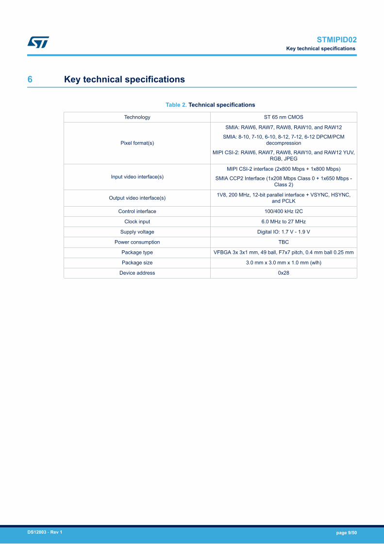
6 Key technical specifications
Table 2. Technical specifications
Technology ST 65 nm CMOS
Pixel format(s)
SMIA: RAW6, RAW7, RAW8, RAW10, and RAW12
SMIA: 8-10, 7-10, 6-10, 8-12, 7-12, 6-12 DPCM/PCMdecompression
MIPI CSI-2: RAW6, RAW7, RAW8, RAW10, and RAW12 YUV,RGB, JPEG
Input video interface(s)MIPI CSI-2 interface (2x800 Mbps + 1x800 Mbps)
SMIA CCP2 Interface (1x208 Mbps Class 0 + 1x650 Mbps -Class 2)
Output video interface(s) 1V8, 200 MHz, 12-bit parallel interface + VSYNC, HSYNC,and PCLK
Control interface 100/400 kHz I2C
Clock input 6.0 MHz to 27 MHz
Supply voltage Digital IO: 1.7 V - 1.9 V
Power consumption TBC
Package type VFBGA 3x 3x1 mm, 49 ball, F7x7 pitch, 0.4 mm ball 0.25 mm
Package size 3.0 mm x 3.0 mm x 1.0 mm (wlh)
Device address 0x28
STMIPID02Key technical specifications
DS12803 - Rev 1 page 9/50

7 Ball assignment and description
Figure 7. Ball assignment: bottom view (49 balls)
1 2 3 4 5 6 7
G
F
E
D
C
B
ADATA1P2
VDDIN_LDO
CLKP1
DATA1N2
DATA2P1
DATA1P1
DATA1N1
TDO D10 LDO_TST
D0
D5
D9
D7
D2
D1
TCK
GNDE_LDO
DATA2N1
CLKP2
CLKN2
CLKN1
VDDOUT_LDO
VDDE_1V8
GNDE
TDI
TMS
XSDN
HSYNC
VDD_1V2
POR_SGN
VDDE_1V8
ERROR
INT
PCLK
GND_1V2
D11
GNDE
VSYNC
SCL
SDA
D4
D8
D6
D3
GNDE
POR_TST EXTCLK
GND_PHY
Note: The CSI-2 clock lanes must be in the middle of the two data lanes.
Note: The PCLK, HSYNC, VSYNC must be routed in the middle of the output data bus for skew management reasons.
Table 3. Ball description
Ball name Type Description
Power supplies
VDDE_1V8 Power 1V8 digital IO supply
VDDIN_LDO Power 1V8 voltage regulator supply
VDD_1V2 Power 1V2 MIPI D-PHY and digital core supply
GNDE Ground Digital IO ground
GNDE_LDO Ground Voltage regulator ground
GND_PHY Ground D-PHY ground
GND_1V2 Ground Digital core ground
System interface
EXTCLK Input System clock input (for I2C slave), 6.0MHz - 27.0 MHz
ERROR Output Error interrupt, indicates that an error(either D-PHY or protocol) has occurred
INT OutputMIPI CSI-2 short packet received
interrupt, indicates that a short packethas been received
STMIPID02Ball assignment and description
DS12803 - Rev 1 page 10/50
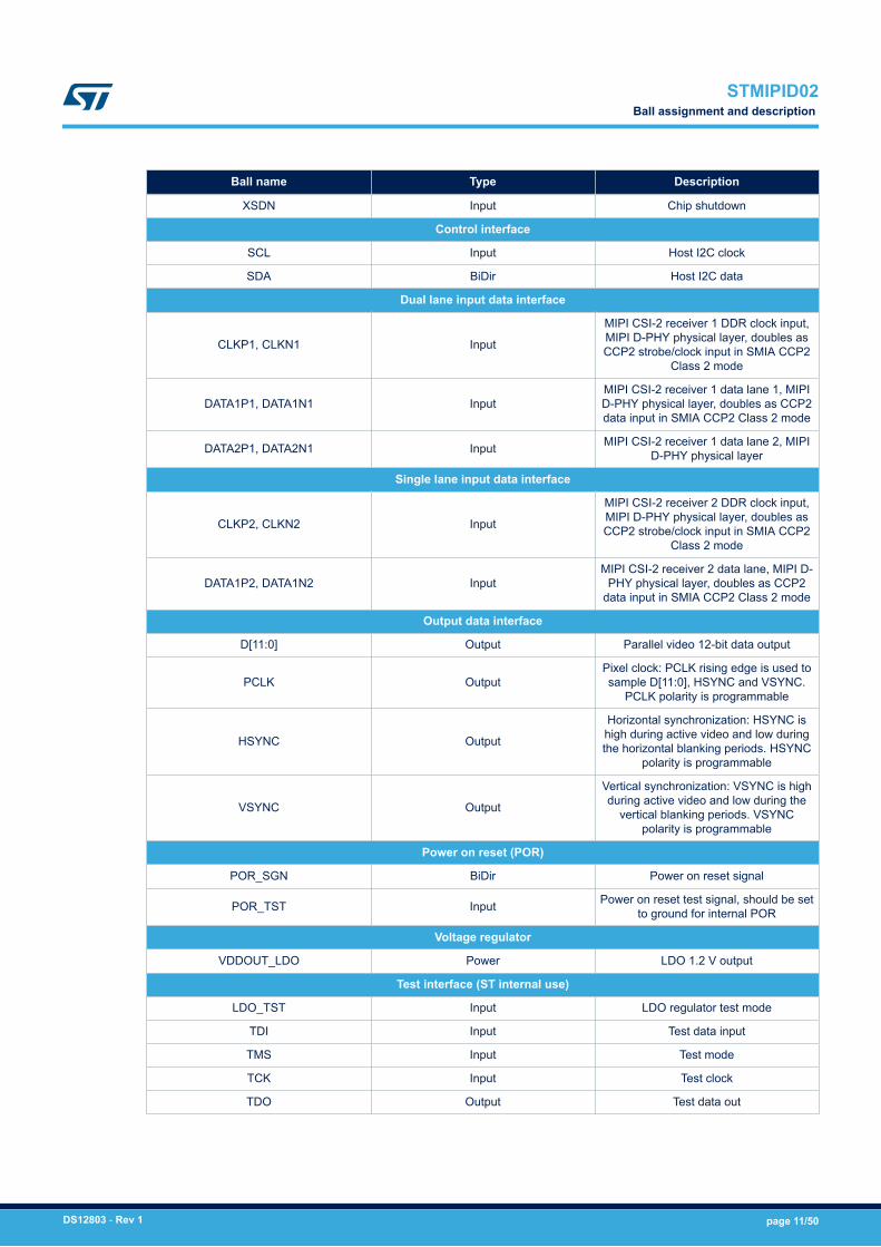
Ball name Type Description
XSDN Input Chip shutdown
Control interface
SCL Input Host I2C clock
SDA BiDir Host I2C data
Dual lane input data interface
CLKP1, CLKN1 Input
MIPI CSI-2 receiver 1 DDR clock input,MIPI D-PHY physical layer, doubles asCCP2 strobe/clock input in SMIA CCP2
Class 2 mode
DATA1P1, DATA1N1 InputMIPI CSI-2 receiver 1 data lane 1, MIPID-PHY physical layer, doubles as CCP2data input in SMIA CCP2 Class 2 mode
DATA2P1, DATA2N1 Input MIPI CSI-2 receiver 1 data lane 2, MIPID-PHY physical layer
Single lane input data interface
CLKP2, CLKN2 Input
MIPI CSI-2 receiver 2 DDR clock input,MIPI D-PHY physical layer, doubles asCCP2 strobe/clock input in SMIA CCP2
Class 2 mode
DATA1P2, DATA1N2 InputMIPI CSI-2 receiver 2 data lane, MIPI D-
PHY physical layer, doubles as CCP2data input in SMIA CCP2 Class 2 mode
Output data interface
D[11:0] Output Parallel video 12-bit data output
PCLK OutputPixel clock: PCLK rising edge is used tosample D[11:0], HSYNC and VSYNC.
PCLK polarity is programmable
HSYNC Output
Horizontal synchronization: HSYNC ishigh during active video and low duringthe horizontal blanking periods. HSYNC
polarity is programmable
VSYNC Output
Vertical synchronization: VSYNC is highduring active video and low during the
vertical blanking periods. VSYNCpolarity is programmable
Power on reset (POR)
POR_SGN BiDir Power on reset signal
POR_TST Input Power on reset test signal, should be setto ground for internal POR
Voltage regulator
VDDOUT_LDO Power LDO 1.2 V output
Test interface (ST internal use)
LDO_TST Input LDO regulator test mode
TDI Input Test data input
TMS Input Test mode
TCK Input Test clock
TDO Output Test data out
STMIPID02Ball assignment and description
DS12803 - Rev 1 page 11/50
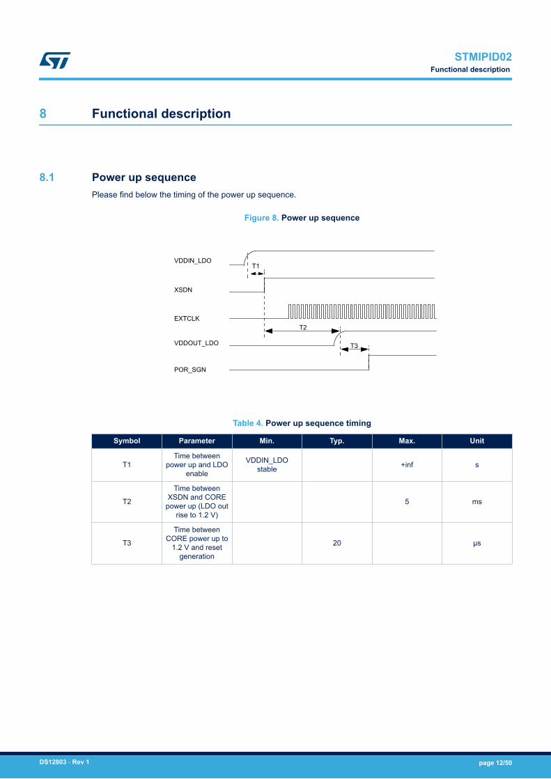
8 Functional description
8.1 Power up sequencePlease find below the timing of the power up sequence.
Figure 8. Power up sequence
VDDIN_LDO
XSDN
EXTCLK
VDDOUT_LDO
POR_SGN
T1
T2
T3
Table 4. Power up sequence timing
Symbol Parameter Min. Typ. Max. Unit
T1Time between
power up and LDOenable
VDDIN_LDOstable +inf s
T2
Time betweenXSDN and CORE
power up (LDO outrise to 1.2 V)
5 ms
T3
Time betweenCORE power up to
1.2 V and resetgeneration
20 µs
STMIPID02Functional description
DS12803 - Rev 1 page 12/50

8.2 User modes
8.2.1 Standard modesThe output parallel interface outputs12 bits of data, HSYNC, VSYNC, and PCLK. It is recommended to enable thecompensation macro (controlled by Mode_Reg3[5], at address 0x36) for both Standard and Bypass modes.
CSI2/CSI2• Main camera: CSI2 up to 1.6 Gbps (with limitation detailed in Section 8.3 CSI2 limitations)• Second camera: CSI2 up to 800 Mbps
CSI2/CCP2• Main camera: CSI2 up to 1.6 Gbps (with limitation detailed in Section 8.3 CSI2 limitations)• Second camera: CCP2 up to 650 Mbps
CSI2/ITU-R601• Main camera: CSI2 up to 1.6 Gbps (with limitation detailed in Section 8.3 CSI2 limitations)• Second camera: YUV directly connected to baseband parallel interface
8.2.2 Bypass modesBypass mode is used for any activities or applications where only PHY is needed, example, 8-bit data.
CSI2/CSI2• Main camera: CSI2 up to 1.6 Gbps (with limitation detailed in Section 8.3 CSI2 limitations)• Second camera: CSI2 up to 800 Mbps
CSI2/ ITU-R601• Main camera: CSI2 up to 1.6 Gbps (with limitation detailed in Section 8.3 CSI2 limitations)• Second camera: YUV directly connected to baseband parallel interface
8.3 CSI2 limitationsThe bandwidth is limited to 800 Mbps in RAW6/RAW7 dual lane inputs. This is irrespective of the compressionused or not
STMIPID02User modes
DS12803 - Rev 1 page 13/50

8.4 Sensor switching mechanismThe flow chart below explains the sensor switching mechanism. If one sensor is streaming and the other is not weare in state1. If both sensors are not streaming, we are in state2.It is forbidden that both sensors stream simultaneously while switching. To switch sensors, it is obligatory to be instate1 or state2 .
Figure 9. Sensor switching mechanism
Stop streaming sensor 1
Reset STMIPID02 with
Program STMIPID02
hard reset
according sensor 2 if needed
Program sensor 2and start streaming
= State 1
= State 2
Sensor 1 streamingSensor 2 stopped
8.5 Error signalBelow is an accumulated status of all errors found in the chip.1. Status of all errors from all D-PHY’s2. Checksum and ECC failures of CSI reception3. ccp_shift_sync, ccp_false_sync and ccp_crc_error of CCP receptionThe individual status of an error can be checked on the respective I2C register bit. The status can be cleared byprogramming Mode_reg2[6] register.
8.6 INT signalThis is a status showing reception of a short packet in the CSI stream. The user needs to clear the status byprogramming Clock_control_reg1[5] to observe the next short packet. If the user does not clear this bit then hemay miss the transition on the INT ball when the next short packet is observed. The application of short packetinterrupts is not envisioned yet.
STMIPID02Sensor switching mechanism
DS12803 - Rev 1 page 14/50

9 Register description
9.1 Clock lane 1 registers
STMIPID02Register description
DS12803 - Rev 1 page 15/50

STMIPID02Clock lane 1 registers
DS12803 - Rev 1 page 16/50

9.2 Data lane 1.1 controls
STMIPID02Data lane 1.1 controls
DS12803 - Rev 1 page 17/50
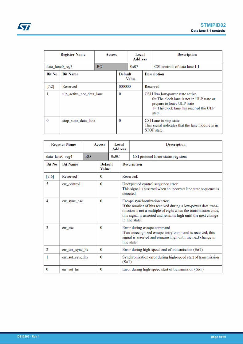
STMIPID02Data lane 1.1 controls
DS12803 - Rev 1 page 18/50

9.3 Data lane 1.2 controls
STMIPID02Data lane 1.2 controls
DS12803 - Rev 1 page 19/50

STMIPID02Data lane 1.2 controls
DS12803 - Rev 1 page 20/50

9.4 Clock lane 2 registers
STMIPID02Clock lane 2 registers
DS12803 - Rev 1 page 21/50

STMIPID02Clock lane 2 registers
DS12803 - Rev 1 page 22/50
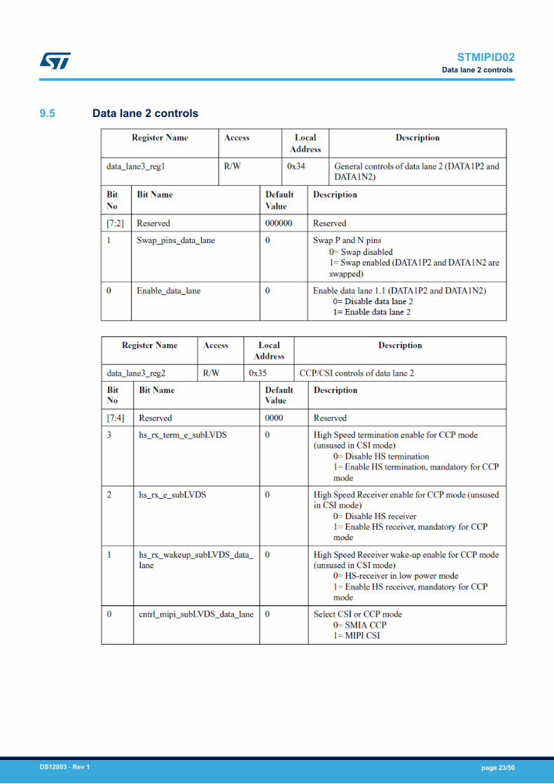
9.5 Data lane 2 controls
STMIPID02Data lane 2 controls
DS12803 - Rev 1 page 23/50

STMIPID02Data lane 2 controls
DS12803 - Rev 1 page 24/50

9.6 CCP RX and error flag registers
STMIPID02CCP RX and error flag registers
DS12803 - Rev 1 page 25/50
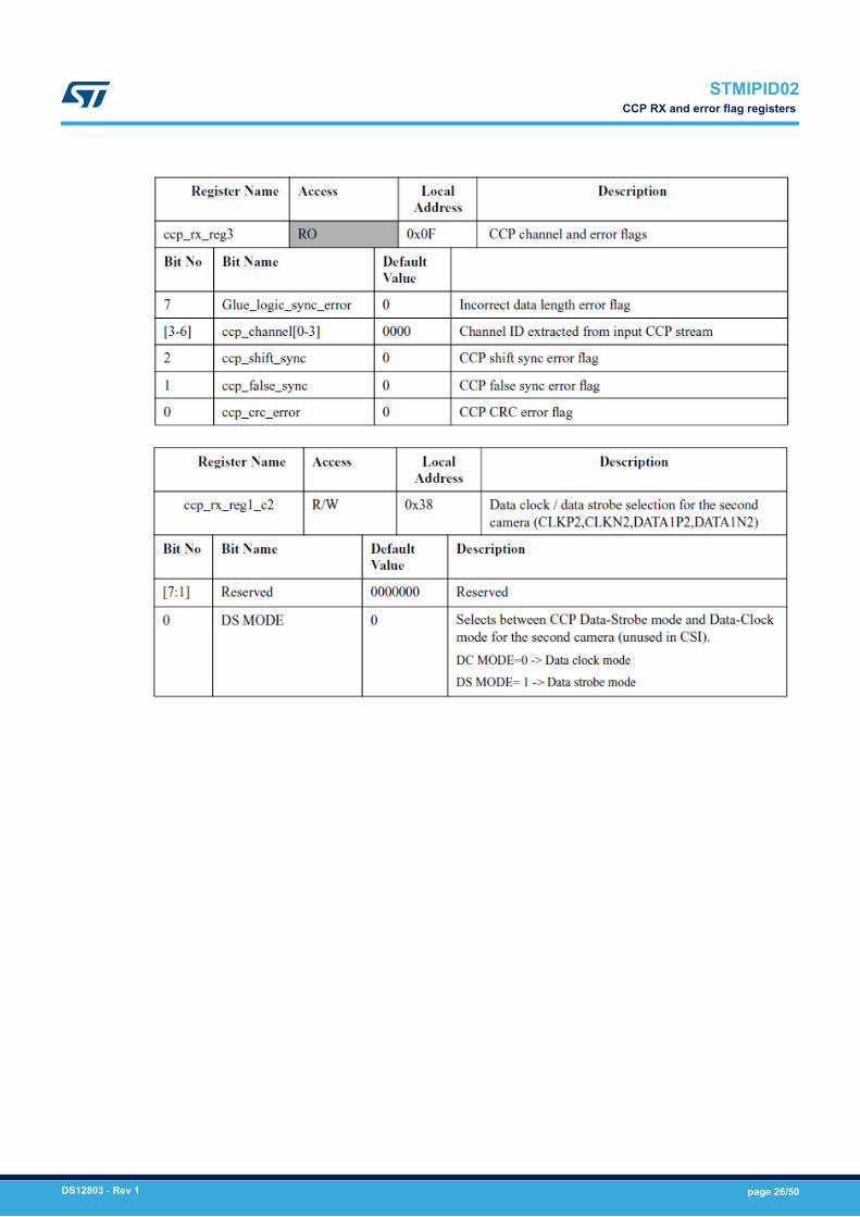
STMIPID02CCP RX and error flag registers
DS12803 - Rev 1 page 26/50

9.7 Mode control registers
STMIPID02Mode control registers
DS12803 - Rev 1 page 27/50

STMIPID02Mode control registers
DS12803 - Rev 1 page 28/50

9.8 Clock control registers
STMIPID02Clock control registers
DS12803 - Rev 1 page 29/50

9.9 System error registers
9.10 Data pipe information
STMIPID02System error registers
DS12803 - Rev 1 page 30/50

STMIPID02Data pipe information
DS12803 - Rev 1 page 31/50

STMIPID02Data pipe information
DS12803 - Rev 1 page 32/50
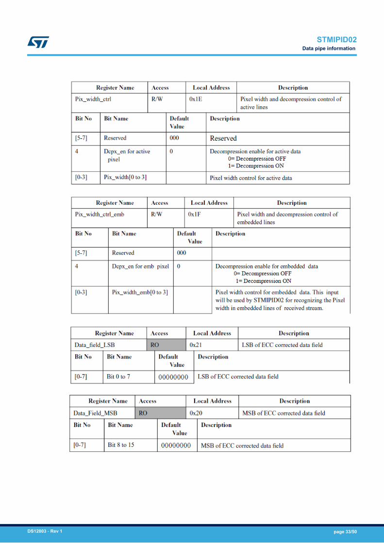
STMIPID02Data pipe information
DS12803 - Rev 1 page 33/50
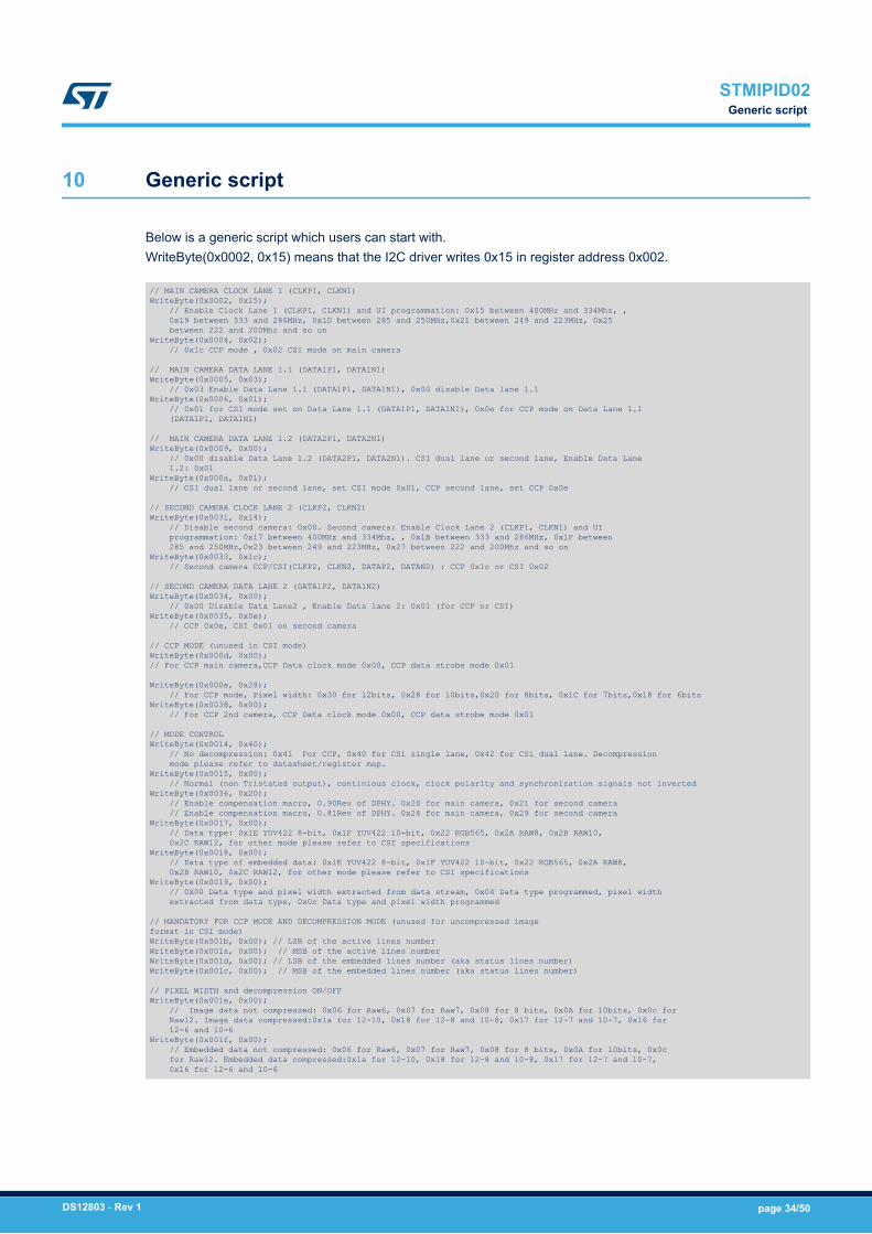
10 Generic script
Below is a generic script which users can start with.WriteByte(0x0002, 0x15) means that the I2C driver writes 0x15 in register address 0x002.
// MAIN CAMERA CLOCK LANE 1 (CLKP1, CLKN1) WriteByte(0x0002, 0x15); // Enable Clock Lane 1 (CLKP1, CLKN1) and UI programmation: 0x15 between 400MHz and 334Mhz, , 0x19 between 333 and 286MHz, 0x1D between 285 and 250MHz,0x21 between 249 and 223MHz, 0x25 between 222 and 200Mhz and so onWriteByte(0x0004, 0x02); // 0x1c CCP mode , 0x02 CSI mode on main camera
// MAIN CAMERA DATA LANE 1.1 (DATA1P1, DATA1N1) WriteByte(0x0005, 0x03); // 0x03 Enable Data Lane 1.1 (DATA1P1, DATA1N1), 0x00 disable Data lane 1.1WriteByte(0x0006, 0x01); // 0x01 for CSI mode set on Data Lane 1.1 (DATA1P1, DATA1N1), 0x0e for CCP mode on Data Lane 1.1 (DATA1P1, DATA1N1)
// MAIN CAMERA DATA LANE 1.2 (DATA2P1, DATA2N1) WriteByte(0x0009, 0x00); // 0x00 disable Data Lane 1.2 (DATA2P1, DATA2N1). CSI dual lane or second lane, Enable Data Lane 1.2: 0x01WriteByte(0x000a, 0x01); // CSI dual lane or second lane, set CSI mode 0x01, CCP second lane, set CCP 0x0e
// SECOND CAMERA CLOCK LANE 2 (CLKP2, CLKN2) WriteByte(0x0031, 0x14); // Disable second camera: 0x00. Second camera: Enable Clock Lane 2 (CLKP1, CLKN1) and UI programmation: 0x17 between 400MHz and 334Mhz, , 0x1B between 333 and 286MHz, 0x1F between 285 and 250MHz,0x23 between 249 and 223MHz, 0x27 between 222 and 200Mhz and so onWriteByte(0x0033, 0x1c); // Second camera CCP/CSI(CLKP2, CLKN2, DATAP2, DATAN2) : CCP 0x1c or CSI 0x02
// SECOND CAMERA DATA LANE 2 (DATA1P2, DATA1N2) WriteByte(0x0034, 0x00); // 0x00 Disable Data Lane2 , Enable Data lane 2: 0x01 (for CCP or CSI)WriteByte(0x0035, 0x0e); // CCP 0x0e, CSI 0x01 on second camera
// CCP MODE (unused in CSI mode) WriteByte(0x000d, 0x00);// For CCP main camera,CCP Data clock mode 0x00, CCP data strobe mode 0x01
WriteByte(0x000e, 0x28); // For CCP mode, Pixel width: 0x30 for 12bits, 0x28 for 10bits,0x20 for 8bits, 0x1C for 7bits,0x18 for 6bitsWriteByte(0x0038, 0x00); // For CCP 2nd camera, CCP Data clock mode 0x00, CCP data strobe mode 0x01
// MODE CONTROL WriteByte(0x0014, 0x40); // No decompression: 0x41 For CCP, 0x40 for CSi single lane, 0x42 for CSi dual lane. Decompression mode please refer to datasheet/register map.WriteByte(0x0015, 0x00); // Normal (non Tristated output), continious clock, clock polarity and synchronization signals not invertedWriteByte(0x0036, 0x20); // Enable compensation macro, 0.90Rev of DPHY. 0x20 for main camera, 0x21 for second camera // Enable compensation macro, 0.81Rev of DPHY. 0x24 for main camera, 0x29 for second cameraWriteByte(0x0017, 0x00); // Data type: 0x1E YUV422 8-bit, 0x1F YUV422 10-bit, 0x22 RGB565, 0x2A RAW8, 0x2B RAW10, 0x2C RAW12, for other mode please refer to CSI specificationsWriteByte(0x0018, 0x00); // Data type of embedded data: 0x1E YUV422 8-bit, 0x1F YUV422 10-bit, 0x22 RGB565, 0x2A RAW8, 0x2B RAW10, 0x2C RAW12, for other mode please refer to CSI specificationsWriteByte(0x0019, 0x00); // 0X00 Data type and pixel width extracted from data stream, 0x04 Data type programmed, pixel width extracted from data type, 0x0c Data type and pixel width programmed
// MANDATORY FOR CCP MODE AND DECOMPRESSION MODE (unused for uncompressed image format in CSI mode)WriteByte(0x001b, 0x00); // LSB of the active lines numberWriteByte(0x001a, 0x00); // MSB of the active lines numberWriteByte(0x001d, 0x00); // LSB of the embedded lines number (aka status lines number) WriteByte(0x001c, 0x00); // MSB of the embedded lines number (aka status lines number)
// PIXEL WIDTH and decompression ON/OFF WriteByte(0x001e, 0x00); // Image data not compressed: 0x06 for Raw6, 0x07 for Raw7, 0x08 for 8 bits, 0x0A for 10bits, 0x0c for Raw12. Image data compressed:0x1a for 12-10, 0x18 for 12-8 and 10-8, 0x17 for 12-7 and 10-7, 0x16 for 12-6 and 10-6WriteByte(0x001f, 0x00); // Embedded data not compressed: 0x06 for Raw6, 0x07 for Raw7, 0x08 for 8 bits, 0x0A for 10bits, 0x0c for Raw12. Embedded data compressed:0x1a for 12-10, 0x18 for 12-8 and 10-8, 0x17 for 12-7 and 10-7, 0x16 for 12-6 and 10-6
STMIPID02Generic script
DS12803 - Rev 1 page 34/50

11 Electrical characteristics
For all CSI2 electrical characteristics, please refer to the MIPI Camera Serial Interface Version 2 (CSI-2).
11.1 Absolute maximum ratings
Table 5. Absolute maximum ratings
Symbol Parameter Value Unit
VDDE_1V8 Digital I/O supply -0.5 to 2.8
VVDDIN_LDO Voltage regulator supply -0.5 to 2.8
Voltage on any signal ball -0.5 to (VDD + 0.5)
IDD Supply current 100mA
Current on any signal ball 10
TSTO Storage temperature -40 to 150˚C
TLEAD Lead temperature (soldering, 10 s) 260
Caution: Stresses above those listed under the “Absolute maximum ratings” may cause permanent damage to the device.This is a stress rating only and functional operation of the device at these or any other conditions above thoseindicated in the operational sections of this specification is not implied. Exposure to absolute maximum ratingconditions for extended periods may affect device reliability.
11.2 Operating conditions
Table 6. Operating conditions
Symbol Parameter Min. Typ. Max. Unit
VDDE_1V8 Digital I/O supply 1.7 1.8 1.9V
VDDIN_LDO Voltage regulator supply 1.7 1.8 1.9
TA Ambient temperature -25 70 °C
CREGLDO output load
capacitor, ESR <1Ω @100 kHz
1 µF
CEXT1.2 V decoupling
capacitor 10 nF
11.3 Thermal data
Table 7. Thermal data
Symbol Parameter Value Unit
Rth(j-a) Max. junction-ambient thermal resistance - VFBGA49 (1) 58.4 ˚C/W
1. Typical, measured with the component mounted on an evaluation PC board in free air
STMIPID02Electrical characteristics
DS12803 - Rev 1 page 35/50
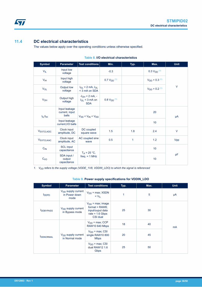
11.4 DC electrical characteristicsThe values below apply over the operating conditions unless otherwise specified.
Table 8. I/O electrical characteristics
Symbol Parameter Test conditions Min. Typ. Max. Unit
VILInput lowvoltage -0.3 0.3 VDD (1)
V
VIHInput high
voltage 0.7 VDD (1) VDD + 0.3 (1)
VOLOutput low
voltageIOL < 2 mA, IOL< 3 mA on SDA
VDD + 0.2 (1)
VOHOutput high
voltage
-IOH < 2 mA, -IOL < 3 mA on
SDA0.8 VDD (1)
IIL/IIH
Input leakagecurrent, input
balls VSS < VIN < VDD
20µA
Input leakagecurrent,I/O balls 10
VEXTCLKDCClock input
amplitude, DCDC coupledsquare wave 1.5 1.8 2.4 V
VEXTCLKACClock input
amplitude, ACAC coupled sine
wave 0.5 1 1.2 Vpp
CINSCL input
capacitanceTA = 25 °C,
freq. = 1 MHz
10
pFCI/O
SDA input /output
capacitance10
1. VDD refers to the supply voltage (VDDE_1V8, VDDIN_LDO) to which the signal is referenced
Table 9. Power supply specifications for VDDIN_LDO
Symbol Parameter Test conditions Typ. Max. Unit
IDDPD
VDD supply currentin Power down
mode
VDD = max; XSDN< VIL
1 5 µA
IDDBYPASSVDD supply current
in Bypass mode
VDD = max; imageformat = RAW8;input/ouput datarate = 1.6 Gbps
CSI dual
25 30
mA
IDDNORMALVDD supply current
in Normal mode
VDD = max; CCPRAW10 640 Mbps 18 40
VDD = max; CSIsingle RAW10 800
Mbps20 45
VDD = max; CSIdual RAW12 1.6
Gbps25 50
STMIPID02DC electrical characteristics
DS12803 - Rev 1 page 36/50
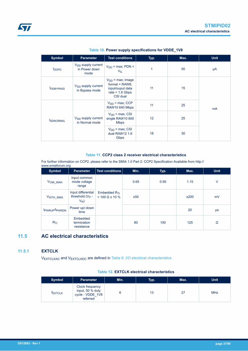
Table 10. Power supply specifications for VDDE_1V8
Symbol Parameter Test conditions Typ. Max. Unit
IDDPD
VDD supply currentin Power down
mode
VDD = max; PDN <VIL
1 50 µA
IDDBYPASSVDD supply current
in Bypass mode
VDD = max; imageformat = RAW8;input/ouput datarate = 1.6 Gbps
CSI dual
11 15
mA
IDDNORMALVDD supply current
in Normal mode
VDD = max; CCPRAW10 640 Mbps 11 25
VDD = max; CSIsingle RAW10 800
Mbps12 25
VDD = max; CSIdual RAW12 1.6
Gbps18 30
Table 11. CCP2 class 2 receiver electrical characteristicsFor further information on CCP2, please refer to the SMIA 1.0 Part 2: CCP2 Specification Available from http://www.smiaforum.org
Symbol Parameter Test conditions Min. Typ. Max. Unit
VCMI_SMIAInput commonmode voltage
range
Embedded RTI= 100 Ω ± 10 %
0.65 0.95 1.15 V
VIDTH_SMIA
Input differentialthreshold (VP -
VN)±50 ±200 mV
tPWRUP/tPWRDNPower up/-down
time 20 µs
RTIEmbeddedterminationresistance
80 100 125 Ω
11.5 AC electrical characteristics
11.5.1 EXTCLKVEXTCLKAC and VEXTCLKDC are defined in Table 8. I/O electrical characteristics
Table 12. EXTCLK electrical characteristics
Symbol Parameter Min. Typ. Max. Unit
fEXTCLK
Clock frequencyinput, 50 % duty
cycle - VDDE_1V8referred
6 13 27 MHz
STMIPID02AC electrical characteristics
DS12803 - Rev 1 page 37/50
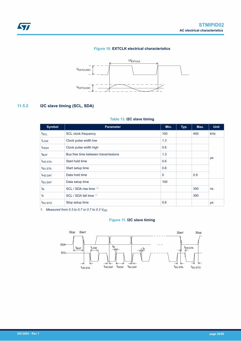
Figure 10. EXTCLK electrical characteristics
1/fEXTCLK
VEXTCLKDC
VEXTCLKAC
11.5.2 I2C slave timing (SCL, SDA)
Table 13. I2C slave timing
Symbol Parameter Min. Typ. Max. Unit
fSCL SCL clock frequency 100 400 kHz
tLOW Clock pulse width low 1.3
µs
tHIGH Clock pulse width high 0.6
tBUF Bus free time between transmissions 1.3
tHD.STA Start hold time 0.6
tSU.STA Start setup time 0.6
tHD.DAT Data hold time 0 0.9
tSU.DAT Data setup time 100
nstR SCL / SDA rise time (1) 300
tF SCL / SDA fall time (1) 300
tSU.STO Stop setup time 0.6 µs
1. Measured from 0.3 to 0.7 or 0.7 to 0.3 VDD
Figure 11. I2C slave timing
Stop Start
tBUF tLOWtR tF
tHIGHtHD.STA tHD.DAT tSU.DAT tSU.STA
tHD.STA
tSU.STO
SCL
SDA
Start Stop
STMIPID02AC electrical characteristics
DS12803 - Rev 1 page 38/50
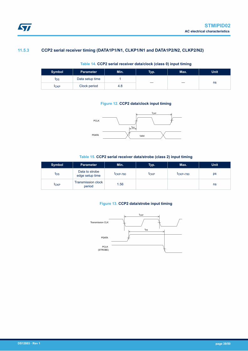
11.5.3 CCP2 serial receiver timing (DATA1P1/N1, CLKP1/N1 and DATA1P2/N2, CLKP2/N2)
Table 14. CCP2 serial receiver data/clock (class 0) input timing
Symbol Parameter Min. Typ. Max. Unit
tDS Data setup time 1— — ns
tCKP Clock period 4.8
Figure 12. CCP2 data/clock input timing
PCLK
tDS
tCKP
PDATA Valid
Table 15. CCP2 serial receiver data/strobe (class 2) input timing
Symbol Parameter Min. Typ. Max. Unit
tDSData to strobe
edge setup time tCKP-780 tCKP tCKP+780 ps
tCKPTransmission clock
period 1.56 ns
Figure 13. CCP2 data/strobe input timing
Transmission CLK
tDS
tCKP
PDATA
PCLK(STROBE)
STMIPID02AC electrical characteristics
DS12803 - Rev 1 page 39/50

11.5.4 Parallel output interface timing
Figure 14. Parallel output interface timing diagram - inverted clock
1/fPCLK
PCLK
D[11:0],HSYNC, VSYNC
tDV
Valid
tR
Figure 15. Parallel output interface timing diagram - non inverted clock
1/fPCLK
PCLK
D[11:0],HSYNC, VSYNC
tDV
Valid
tF
Note: For Non-inverted clock mode, the valid edge to capture is the negative (falling) edgeFor RAW6/RAW7 dual lane, the bandwith is limited to 800 Mbps.
Table 16. Parallel output interface timing
Symbol Description Conditions Min. Typ. Max. Unit
fPCLK PCLK frequency 200 MHz
DPCLKPCLK duty
cycle
No bypass,RAW6 dual lane 50
%
No bypass,RAW7 dual lane 66
No bypass,RAW7 duallane, jittered
clock
50-60
No bypass,RAW7 single
lane57.14
Bypass and allother modes 45 50 55
tRPCLK rise time,
20 % - 80 %
Loadcapacitance, CL
= 50 pF2.1
ns
tDVPCLK to output
valid 0 2
STMIPID02AC electrical characteristics
DS12803 - Rev 1 page 40/50
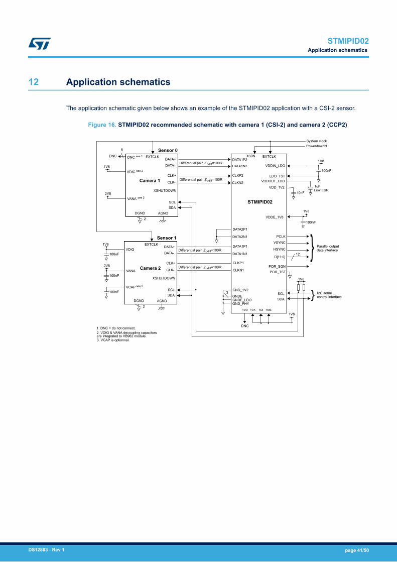
12 Application schematics
The application schematic given below shows an example of the STMIPID02 application with a CSI-2 sensor.
Figure 16. STMIPID02 recommended schematic with camera 1 (CSI-2) and camera 2 (CCP2)
Camera 1
EXTCLKDATA+
CLK-
DATA1P2
CLKP2
STMIPID02
EXTCLK
System clockPowerdownN
TCK TDI TMS
XSDN
DATA1N2
CLKN2
XSHUTDOWN
VDDOUT_LDO
DATA-
CLK+
TDO
DATA1P1
CLKP1
DATA1N1
CLKN1
GND_1V2
LDO_TST
DNC
1V8
Differential pair, Zodiff=100R
Differential pair, Zodiff=100R
1uFLow ESR
VDIG see 2
DNC see 1
DGND
VANA see 2
1V8
2V8
2
DNC
AGND
1V8
100nFVDDIN_LDO
VDDE_1V8
1V8
100nF
GNDE3
GNDE_LDOGND_PHY
Sensor 0
1. DNC = do not connect.
VDD_1V2
DATA2P1
DATA2N1
D[11:0]
PCLK
VSYNC
HSYNC12 } Parallel output
data interface
SDASCL
1V8
SDASCL
} I2C serialcontrol interface
5
2. VDIG & VANA decoupling capacitorsare integrated to VB962 module.
10nF
Camera 2
EXTCLKDATA+
CLK-
XSHUTDOWN
DATA-
CLK+
VDIG
DGND
VANA
1V8
2V8
2AGND
Sensor 1
SDASCL
Differential pair, Zodiff=100R
Differential pair, Zodiff=100R
100nF
VCAP see 3
100nF
100nF
3. VCAP is optionnal.
POR_SGNPOR_TST
STMIPID02Application schematics
DS12803 - Rev 1 page 41/50
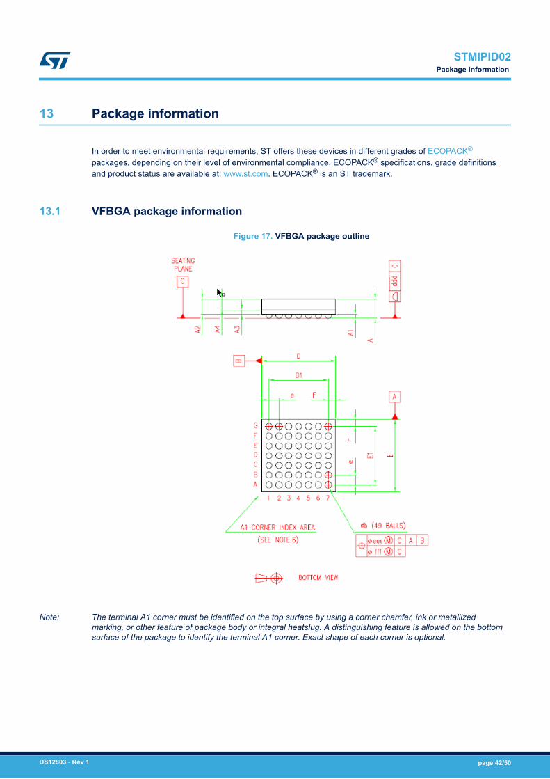
13 Package information
In order to meet environmental requirements, ST offers these devices in different grades of ECOPACK®
packages, depending on their level of environmental compliance. ECOPACK® specifications, grade definitionsand product status are available at: www.st.com. ECOPACK® is an ST trademark.
13.1 VFBGA package information
Figure 17. VFBGA package outline
Note: The terminal A1 corner must be identified on the top surface by using a corner chamfer, ink or metallizedmarking, or other feature of package body or integral heatslug. A distinguishing feature is allowed on the bottomsurface of the package to identify the terminal A1 corner. Exact shape of each corner is optional.
STMIPID02Package information
DS12803 - Rev 1 page 42/50

Table 17. VFBGA mechanical data
Reference
Dimensions
Millimeters Inches
Min. Typ. Max. Min. Typ. Max.
A (1) 1.00 0.039
A1 0.125 0.005
A2 0.615 0.024
A3 0.18 0.007
A4 0.45 0.018
b (2) 0.22 0.26 0.30 0.009 0.010 0.012
D 2.95 3.00 3.05 0.116 0.118 0.120
D1 2.40 0.094
E 2.95 3.00 3.05 0.116 0.118 0.120
E1 2.40 0.094
e 0.40 0.016
F 0.30 0.012
ddd 0.08 0.003
eee (3) 0.13 0.005
fff (4) 0.04 0.002
1. VFBGA stands for very thin profile fine pitch ball grid array. Very thin profile: 0.80 mm < A ≤ 1.00 mm / fine pitch: e < 1.00mm. The maximum total package height is calculated by the following methodology: A2 Typ. + A1 Typ. + square-root(A1+A3 +A4 tolerance values).
2. The typical ball diameter before mounting is 0.25 mm.3. The tolerance of the position that controls the location of the pattern of balls with respect to datums A and B. For each ball
there is a cylindrical tolerance zone, eee, perpendicular to datum C and located on the true position with respect to datumsA and B as defined by e. The axis perpendicular to datum C of each ball must lie within this tolerance zone.
4. The tolerance of the position that controls the location of the balls within the matrix with respect to each other. For each ball,there is a cylindrical tolerance zone, fff, perpendicular to datum C and located on the true position as defined by e. The axisperpendicular to datum C of each ball must lie within this tolerance zone. Each tolerance zone fff in the array is containedentirely in the respective zone eee above. The axis of each ball must lie simultaneously in both tolerance zones.
STMIPID02VFBGA package information
DS12803 - Rev 1 page 43/50
14 PCB layout guide
The usual good PCB design rules should be observed for the layout of the STMIPID02.Power and ground planes should be used to supply power to the STMIPID02.The high-speed signal pairs (CLKP1, CLKN1), (DATA1P1, DATA1N1), (DATA2P1, DATA2N1), (CLKP2, CLKN2)and (DATA1P2, DATA1N2) should be routed as balanced transmission lines with a characteristic differentialimpedance (Zodiff) of 100 Ω, and matched in length.The delay difference between Cclock lane, data lane1 and data lane2 should be less than 5 ps.The total series resistance of the CSI line should be less than 5 Ω.For more details, please refer to the MIPI Alliance Specification for D-PHY”, version 0.90.00, 8 October 2007,Section 7 "Interconnect and Lane Configuration" and Annex B "Interconnect Design Guidelines".The output interface clock (PCLK) should be 50 Ω adapted.The output clock (PCLK) and data line length from the STMIPID02 to the host should be as small as possible toavoid reflection effects.All passive components for the STMIPID02 should be placed in close proximity to the device, including thedecoupling capacitors.The recommended pull up value of the I2C is in the range 2480 Ω to2780 Ω for a bus load capacitance below 100pF.The recommended capacitor values are:• 10 nF on VDD1V2• 100 nF on VDDIN_LDO and VDDE_1V8• 1 µF (low ESR <1 Ω) on VDDOUT_LDO
STMIPID02PCB layout guide
DS12803 - Rev 1 page 44/50
15 ESD characteristics
The device ESD sensitivity is compliant with the following specifications:• JESD22 A114D, human body model, ±2 kV, class 2 compliant• JESD22-C101C, charge device model, ±500 V, class III compliant
STMIPID02ESD characteristics
DS12803 - Rev 1 page 45/50

16 Ordering information
Table 18. Order code
Sales type Package
STMIPID02/TR VFBGA 49 ball, 3 mm x 3 mm x 1 mm, 0.4 mm pitch, 0.25 mmball package
STMIPID02Ordering information
DS12803 - Rev 1 page 46/50

Revision history
Table 19. Document revision history
Date Version Changes
22-Oct-2018 1 Initial public release
STMIPID02
DS12803 - Rev 1 page 47/50

Contents
1 Block diagram . . . . . . . . . . . . . . . . . . . . . . . . . . . . . . . . . . . . . . . . . . . . . . . . . . . . . . . . . . . . . . . . . . . . .3
2 Application diagrams . . . . . . . . . . . . . . . . . . . . . . . . . . . . . . . . . . . . . . . . . . . . . . . . . . . . . . . . . . . . . .4
3 Output interface . . . . . . . . . . . . . . . . . . . . . . . . . . . . . . . . . . . . . . . . . . . . . . . . . . . . . . . . . . . . . . . . . . .5
4 Control interface. . . . . . . . . . . . . . . . . . . . . . . . . . . . . . . . . . . . . . . . . . . . . . . . . . . . . . . . . . . . . . . . . . .7
5 Application examples. . . . . . . . . . . . . . . . . . . . . . . . . . . . . . . . . . . . . . . . . . . . . . . . . . . . . . . . . . . . . .8
6 Key technical specifications . . . . . . . . . . . . . . . . . . . . . . . . . . . . . . . . . . . . . . . . . . . . . . . . . . . . . . .9
7 Ball assignment and description . . . . . . . . . . . . . . . . . . . . . . . . . . . . . . . . . . . . . . . . . . . . . . . . . .10
8 Functional description . . . . . . . . . . . . . . . . . . . . . . . . . . . . . . . . . . . . . . . . . . . . . . . . . . . . . . . . . . . .12
8.1 Power up sequence . . . . . . . . . . . . . . . . . . . . . . . . . . . . . . . . . . . . . . . . . . . . . . . . . . . . . . . . . . . 12
8.2 User modes . . . . . . . . . . . . . . . . . . . . . . . . . . . . . . . . . . . . . . . . . . . . . . . . . . . . . . . . . . . . . . . . . . 13
8.2.1 Standard modes . . . . . . . . . . . . . . . . . . . . . . . . . . . . . . . . . . . . . . . . . . . . . . . . . . . . . . . . 13
8.2.2 Bypass modes . . . . . . . . . . . . . . . . . . . . . . . . . . . . . . . . . . . . . . . . . . . . . . . . . . . . . . . . . 13
8.3 CSI2 limitations . . . . . . . . . . . . . . . . . . . . . . . . . . . . . . . . . . . . . . . . . . . . . . . . . . . . . . . . . . . . . . . 13
8.4 Sensor switching mechanism . . . . . . . . . . . . . . . . . . . . . . . . . . . . . . . . . . . . . . . . . . . . . . . . . . . 14
8.5 Error signal. . . . . . . . . . . . . . . . . . . . . . . . . . . . . . . . . . . . . . . . . . . . . . . . . . . . . . . . . . . . . . . . . . . 14
8.6 INT signal . . . . . . . . . . . . . . . . . . . . . . . . . . . . . . . . . . . . . . . . . . . . . . . . . . . . . . . . . . . . . . . . . . . . 14
9 Register description . . . . . . . . . . . . . . . . . . . . . . . . . . . . . . . . . . . . . . . . . . . . . . . . . . . . . . . . . . . . . .15
9.1 Clock lane 1 registers . . . . . . . . . . . . . . . . . . . . . . . . . . . . . . . . . . . . . . . . . . . . . . . . . . . . . . . . . . 15
9.2 Data lane 1.1 controls. . . . . . . . . . . . . . . . . . . . . . . . . . . . . . . . . . . . . . . . . . . . . . . . . . . . . . . . . . 16
9.3 Data lane 1.2 controls. . . . . . . . . . . . . . . . . . . . . . . . . . . . . . . . . . . . . . . . . . . . . . . . . . . . . . . . . . 18
9.4 Clock lane 2 registers . . . . . . . . . . . . . . . . . . . . . . . . . . . . . . . . . . . . . . . . . . . . . . . . . . . . . . . . . . 20
9.5 Data lane 2 controls . . . . . . . . . . . . . . . . . . . . . . . . . . . . . . . . . . . . . . . . . . . . . . . . . . . . . . . . . . . 22
9.6 CCP RX and error flag registers . . . . . . . . . . . . . . . . . . . . . . . . . . . . . . . . . . . . . . . . . . . . . . . . . 24
9.7 Mode control registers . . . . . . . . . . . . . . . . . . . . . . . . . . . . . . . . . . . . . . . . . . . . . . . . . . . . . . . . . 26
9.8 Clock control registers . . . . . . . . . . . . . . . . . . . . . . . . . . . . . . . . . . . . . . . . . . . . . . . . . . . . . . . . . 29
9.9 System error registers . . . . . . . . . . . . . . . . . . . . . . . . . . . . . . . . . . . . . . . . . . . . . . . . . . . . . . . . . 29
9.10 Data pipe information . . . . . . . . . . . . . . . . . . . . . . . . . . . . . . . . . . . . . . . . . . . . . . . . . . . . . . . . . . 30
10 Generic script . . . . . . . . . . . . . . . . . . . . . . . . . . . . . . . . . . . . . . . . . . . . . . . . . . . . . . . . . . . . . . . . . . . .34
11 Electrical characteristics. . . . . . . . . . . . . . . . . . . . . . . . . . . . . . . . . . . . . . . . . . . . . . . . . . . . . . . . . .35
STMIPID02Contents
DS12803 - Rev 1 page 48/50

11.1 Absolute maximum ratings. . . . . . . . . . . . . . . . . . . . . . . . . . . . . . . . . . . . . . . . . . . . . . . . . . . . . . 35
11.2 Operating conditions. . . . . . . . . . . . . . . . . . . . . . . . . . . . . . . . . . . . . . . . . . . . . . . . . . . . . . . . . . . 35
11.3 Thermal data . . . . . . . . . . . . . . . . . . . . . . . . . . . . . . . . . . . . . . . . . . . . . . . . . . . . . . . . . . . . . . . . . 35
11.4 DC electrical characteristics. . . . . . . . . . . . . . . . . . . . . . . . . . . . . . . . . . . . . . . . . . . . . . . . . . . . . 35
11.5 AC electrical characteristics. . . . . . . . . . . . . . . . . . . . . . . . . . . . . . . . . . . . . . . . . . . . . . . . . . . . . 37
11.5.1 EXTCLK . . . . . . . . . . . . . . . . . . . . . . . . . . . . . . . . . . . . . . . . . . . . . . . . . . . . . . . . . . . . . . 37
11.5.2 I2C slave timing (SCL, SDA) . . . . . . . . . . . . . . . . . . . . . . . . . . . . . . . . . . . . . . . . . . . . . . . 38
11.5.3 CCP2 serial receiver timing (DATA1P1/N1, CLKP1/N1 and DATA1P2/N2, CLKP2/N2) . . . 38
11.5.4 Parallel output interface timing . . . . . . . . . . . . . . . . . . . . . . . . . . . . . . . . . . . . . . . . . . . . . 39
12 Application schematics . . . . . . . . . . . . . . . . . . . . . . . . . . . . . . . . . . . . . . . . . . . . . . . . . . . . . . . . . . .41
13 Package information. . . . . . . . . . . . . . . . . . . . . . . . . . . . . . . . . . . . . . . . . . . . . . . . . . . . . . . . . . . . . .42
13.1 [Package name] package information . . . . . . . . . . . . . . . . . . . . . . . . . . . . . . . . . . . . . . . . . . . . 42
14 PCB layout guide . . . . . . . . . . . . . . . . . . . . . . . . . . . . . . . . . . . . . . . . . . . . . . . . . . . . . . . . . . . . . . . . .44
15 ESD characteristics. . . . . . . . . . . . . . . . . . . . . . . . . . . . . . . . . . . . . . . . . . . . . . . . . . . . . . . . . . . . . . .45
16 Ordering information . . . . . . . . . . . . . . . . . . . . . . . . . . . . . . . . . . . . . . . . . . . . . . . . . . . . . . . . . . . . .46
Revision history . . . . . . . . . . . . . . . . . . . . . . . . . . . . . . . . . . . . . . . . . . . . . . . . . . . . . . . . . . . . . . . . . . . . . . .47
STMIPID02Contents
DS12803 - Rev 1 page 49/50

IMPORTANT NOTICE – PLEASE READ CAREFULLY
STMicroelectronics NV and its subsidiaries (“ST”) reserve the right to make changes, corrections, enhancements, modifications, and improvements to STproducts and/or to this document at any time without notice. Purchasers should obtain the latest relevant information on ST products before placing orders. STproducts are sold pursuant to ST’s terms and conditions of sale in place at the time of order acknowledgement.
Purchasers are solely responsible for the choice, selection, and use of ST products and ST assumes no liability for application assistance or the design ofPurchasers’ products.
No license, express or implied, to any intellectual property right is granted by ST herein.
Resale of ST products with provisions different from the information set forth herein shall void any warranty granted by ST for such product.
ST and the ST logo are trademarks of ST. All other product or service names are the property of their respective owners.
Information in this document supersedes and replaces information previously supplied in any prior versions of this document.
© 2018 STMicroelectronics – All rights reserved
STMIPID02
DS12803 - Rev 1 page 50/50