david culler electrical engineering and computer sciences university of california, berkeley
DESCRIPTION
EECS 150 - Components and Design Techniques for Digital Systems Lec 21 – RTL Design Optimization 11/16/2004. David Culler Electrical Engineering and Computer Sciences University of California, Berkeley http://www.eecs.berkeley.edu/~culler http://www-inst.eecs.berkeley.edu/~cs150. - PowerPoint PPT PresentationTRANSCRIPT

1
EECS 150 - Components and Design
Techniques for Digital Systems
Lec 21 – RTL Design Optimization
11/16/2004
David CullerElectrical Engineering and Computer Sciences
University of California, Berkeley
http://www.eecs.berkeley.edu/~cullerhttp://www-inst.eecs.berkeley.edu/~cs150
2
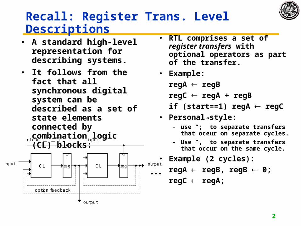
Recall: Register Trans. Level Descriptions
• A standard high-level representation for describing systems.
• It follows from the fact that all synchronous digital system can be described as a set of state elements connected by combination logic (CL) blocks:
• RTL comprises a set of register transfers with optional operators as part of the transfer.
• Example:
regA regB
regC regA + regB
if (start==1) regA regC
• Personal style:– use “;” to separate transfers that
occur on separate cycles.
– Use “,” to separate transfers that occur on the same cycle.
• Example (2 cycles):
regA regB, regB 0;
regC regA;
reg regCL CL
clock input
output
option feedback
input output

3
Components of the data path
• Storage– Flip-flops– Registers– Register Files– SRAM
• Arithmetic Units– Adders, subtraters, ALUs (built out of FAs or gates)– Comparators– Counters
• Interconnect– Wires– Busses– Tri-state Buffers– MUX

4
Arithmetic Circuit Design (MT revisited)
• Full Adder
• Adder
• Relationship of positional notation and operations on it to arithmetic circuits
FA
A B Cin
Co S
5
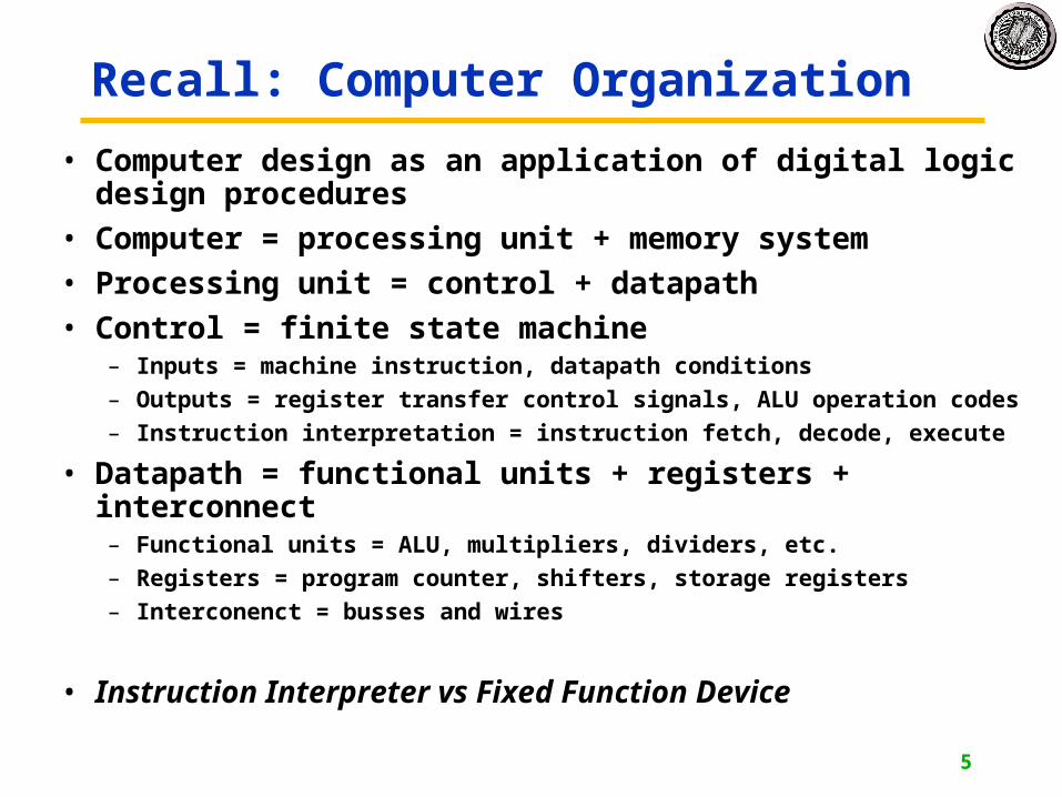
Recall: Computer Organization
• Computer design as an application of digital logic design procedures
• Computer = processing unit + memory system
• Processing unit = control + datapath
• Control = finite state machine– Inputs = machine instruction, datapath conditions
– Outputs = register transfer control signals, ALU operation codes
– Instruction interpretation = instruction fetch, decode, execute
• Datapath = functional units + registers + interconnect– Functional units = ALU, multipliers, dividers, etc.
– Registers = program counter, shifters, storage registers
– Interconenct = busses and wires
• Instruction Interpreter vs Fixed Function Device
6
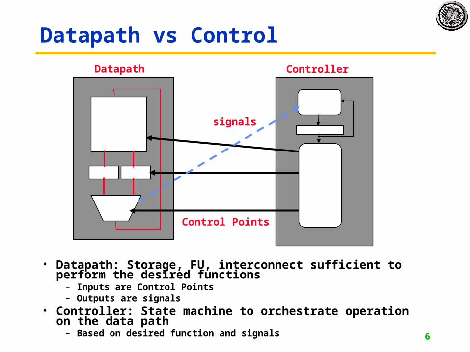
Datapath vs Control
• Datapath: Storage, FU, interconnect sufficient to perform the desired functions
– Inputs are Control Points– Outputs are signals
• Controller: State machine to orchestrate operation on the data path
– Based on desired function and signals
Datapath Controller
Control Points
signals

7
Vector Op Example (more MT)

8
List Processor Example
• RTL gives us a framework for making high-level optimizations.– Fixed function unit– Approach extends to instruction interpreters
• General design procedure outline:1. Problem, Constraints, and Component Library Spec.2. “Algorithm” Selection3. Micro-architecture Specification4. Analysis of Cost, Performance, Power5. Optimizations, Variations6. Detailed Design

9
1. Problem Specification
• Design a circuit that forms the sum of all the 2's complements integers stored in a linked-list structure starting at memory address 0:
• All integers and pointers are 8-bit. The link-list is stored in a memory block with an 8-bit address port and 8-bit data port, as shown below. The pointer from the last element in the list is 0. At least one node in list.
I/Os:– START resets to head of list
and starts addition process.
– DONE signals completion
– R, Bus that holds the final result

10
1. Other Specifications
• Design Constraints:– Usually the design specification puts a restriction on cost,
performance, power or all. We will leave this unspecified for now and return to it later.
• Component Library:component delay
simple logic gates 0.5nsn-bit register clk-to-Q=0.5ns
setup=0.5ns (data and LD)n-bit 2-1 multiplexor 1nsn-bit adder (2 log(n) + 2)nsmemory 10ns read (asynchronous read)zero compare 0.5 log(n)
(single ported memory)
Are these reasonable?

11
2. Algorithm Specification
• In this case the memory only allows one access per cycle, so the algorithm is limited to sequential execution. If in another case more input data is available at once, then a more parallel solution may be possible.
• Assume datapath state registers NEXT and SUM.– NEXT holds a pointer to the node in memory.
– SUM holds the result of adding the node values to this point.
If (START==1) NEXT0, SUM0;
repeat {
SUMSUM + Memory[NEXT+1];
NEXTMemory[NEXT];
} until (NEXT==0);
RSUM, DONE1;

12
A_SEL01
NEXT0
1
+
Memory
D
A
==0
+
01
SUM
NEXT_SEL
LD_NEXT
NEXT_ZERO
SUM_SEL
LD_SUM
0
1
0
3. Architecture #1Direct implementation of RTL description:
Datapath
Controller
If (START==1) NEXT0, SUM0; repeat { SUMSUM + Memory[NEXT+1]; NEXTMemory[NEXT];
} until (NEXT==0);RSUM, DONE1;

13
4. Analysis of Cost, Performance, and Power
• Skip Power for now.
• Cost:– How do we measure it? # of transistors? # of gates? # of CLBs?
– Depends on implementation technology. Usually we are interested in comparing the relative cost of two competing implementations. (Save this for later)
• Performance:– 2 clock cycles per number added.
– What is the minimum clock period?
– The controller might be on the critical path. Therefore we need to know the implementation, and controller input and output delay.

14
Possible Controller Implementation
START
COMPSUM
GETNEXT
DONE
LD_SUM
SUM_SEL
LD_NEXT
NEXT_SEL
DONE
A_SEL
START
START
START
NEXT_ZERO
• Based on this, what is the controller input and output delay?

15
MT again…
• Longest path from any reg out to any reg input
3
2
2
4
11
D Q
D Q
D Q
D Q
16
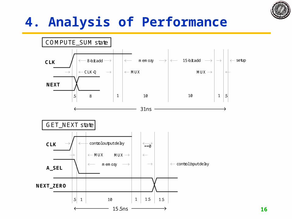
4. Analysis of Performance
CLK-Q MUX
8-bit add memory 15-bit add
MUX
setup
.5 8 1 10 10 1 .5
31ns
CLK
NEXT
CLK
A_SEL
MUX
control output delay
memory
MUX
==0
control input delay
.5 101 1.51 1.5
15.5ns
COMPUTE_SUM state
GET_NEXT state
NEXT_ZERO

17
Critical paths
A_SEL01
NEXT0
1
+
Memory
D
A
==0
+
01
SUM
NEXT_SEL
LD_NEXT
NEXT_ZERO
SUM_SEL
LD_SUM
0
1
0

18
4. Analysis of Performance• Detailed timing:
clock period (T) = max (clock period for each state)
T > 31ns, F < 32 MHz
• Observation:COMPUTE_SUM state does most of the work. Most of the components
are inactive in GET_NEXT state.
GET_NEXT does: Memory access + …
COMPUTE_SUM does: 8-bit add, memory access, 15-bit add + …
• Conclusion:Move one of the adds to GET_NEXT.

19
5. Optimization
• Add new register named NUMA, for address of number to add.
• Update RTL to reflect our change (note still 2 cycles per iteration):
If (START==1) NEXT0, SUM0, NUMA1;
repeat {
SUMSUM + Memory[NUMA];
NUMAMemory[NEXT] + 1,
NEXTMemory[NEXT] ;
} until (NEXT==0);
RSUM, DONE1;

20
5. Optimization
• Architecture #2:
• Incremental cost: addition of another register and mux.
If (START==1) NEXT0, SUM0, NUMA1; repeat { SUMSUM + Memory[NUMA]; NUMAMemory[NEXT] + 1, NEXTMemory[NEXT] ; } until (NEXT==0); RSUM, DONE1;
A_SEL01
NEXT0
1
+
Memory
D
A
==0
+
01
SUM
NEXT_SEL
LD_NEXT
NEXT_ZERO
SUM_SEL
LD_SUM
0
1
0
01
NUMA
NEXT_SEL
LD_NEXT
1

21
5. Optimization, Architecture #2• New timing:
Clock Period (T) = max (clock period for each state)
T > 23ns, F < 43Mhz
• Is this worth the extra cost?
• Can we lower the cost?
• Notice that the circuit now only performs one add on every cycle. Why not share the adder for both cycles?
CLK-Q
MUX
memory15-bit add
MUX
setup
.5 1 10 10 1 .5
23ns
CLK
NUMA
CLK
A_SEL
MUX
control output delay
memory
MUX
NUMA reg setup
.5 101 .51
21ns
COMPUTE_SUM state
GET_NEXT state
8-bit add
8

22
5. Optimization, Architecture #3
• Incremental cost:– Addition of another mux and control. Removal of an 8-bit adder.
• Performance:– mux adds 1ns to cycle time. 24ns, 41.67MHz.
• Is the cost savings worth the performance degradation?
A_SEL01
NEXT0
1
Memory
D
A
==0
+
01
SUM
NEXT_SEL
LD_NEXT
NEXT_ZERO
SUM_SEL
LD_SUM
0
0
01
NUMA
NEXT_SEL
LD_NEXT
1
01ADD_SEL
1