david j. thomson, ke li, peter r. wilson, sheng-wen chen ... papers/nanopho_breakthroughs in...
TRANSCRIPT

DOI 10.1515/nanoph-2013-0016 Nanophotonics 2014; 3(4-5): 229–245
© 2014 Science Wise Publishing & De Gruyter
Review article
Graham T. Reed*, Goran Z. Mashanovich, Frederic Y. Gardes, Milos Nedeljkovic, Youfang Hu, David J. Thomson, Ke Li, Peter R. Wilson, Sheng-Wen Chen and Shawn S. Hsu
Recent breakthroughs in carrier depletion based silicon optical modulators
Abstract: The majority of the most successful optical modulators in silicon demonstrated in recent years oper-ate via the plasma dispersion effect and are more spe-cifically based upon free carrier depletion in a silicon rib waveguide. In this work we overview the different types of free carrier depletion type optical modulators in silicon. A summary of some recent example devices for each config-uration is then presented together with the performance that they have achieved. Finally an insight into some cur-rent research trends involving silicon based optical modu-lators is provided including integration, operation in the mid-infrared wavelength range and application in short and long haul data transmission links.
Keywords: modulators; silicon photonics; depletion.
*Corresponding author: Graham T. Reed, Optoelectronics Research Centre, University of Southampton, Highfield Campus Southampton, Southampton, Hampshire SO17 1BJ, UK, e-mail: [email protected] Z. Mashanovich, Frederic Y. Gardes, Milos Nedeljkovic, Youfang Hu and David J. Thomson: Optoelectronics Research Centre, University of Southampton, Southampton, Hampshire, SO17 1BJ, UKKe Li and Peter R. Wilson: School of Electronics and Computer Science, University of Southampton, Southampton, Hampshire, SO17 1BJ, UKSheng-Wen Chen and Shawn S. Hsu: High-Speed Devices and Integrated Circuits Group Department of Electrical Engineering, National Tsing Hua University, Hsinchu, Taiwan
Edited by Haiseng Rong
1 IntroductionThe performance of silicon optical modulators has improved dramatically in recent years, coinciding with significant research effort from both academia and commercial organisations worldwide. The motivation for developing high performance optical modulators in silicon is clear. The optical modulator is central to the majority of photonics systems for datacom applications
and silicon photonics provides a low cost platform in which to form these systems, making optical based com-munication feasible for a number of short reach links. Various mechanisms for achieving modulation in silicon have been investigated throughout the years. Excellent progress has been made in hybrid devices where other materials are incorporated with the SOI waveguides to achieve modulation, including group III–V materi-als [1], germanium [2–6], polymers [7, 8] and graphene [9–13]. Furthermore the plasmonic based approach is also interesting area to achieve modulation [14–17]. This review will however focus on devices based upon the plasma dispersion effect and more specifically those using carrier depletion. Plasma dispersion effect devices are attractive as they can be formed using CMOS like processes making their integration into such fabrica-tion facilities more straightforward. Employing carrier depletion as the mechanism to electrically modulate free carrier densities in the waveguide allows relatively simple fabrication whilst achieving high speed. Follow-ing a review of recent carrier depletion devices [18–51] we will look more into the progress of their integration with other components.
2 Performance metricsIt is useful to start by considering the different perfor-mance metrics by which the devices can be assessed. For the phase modulator there are four core metrics: the optical loss and capacitance per unit length, the phase efficiency and the speed. Design choices over the passive structure used to house the phase modulator, the phase modulator length and the drive voltage then dictate what the overall performance of the modulator will be. For example for a Mach-Zehnder modulator, the use of a short phase modulator and a low drive voltage will result in low optical loss and low power consumption. However, the extinction ratio achieved will be lower.
Brought to you by | National Tsing-Hua UniversityAuthenticated
Download Date | 8/15/17 4:35 AM
230 G.T. Reed et al.: Carrier depletion silicon optical modulators
Conversely, if a larger extinction ratio is required either the phase modulator length or the drive voltage can be increased (or a combination of both), although this will result in an increase in optical loss or power consump-tion, respectively. The different performance metrics for the overall modulator structure are listed below with description.
2.1 Modulator drive voltage/power consumption
The power consumption of the device is an important metric to consider particularly in applications which have multiple short-reach channels. The convention with silicon optical modulators is to report the power con-sumption in units of energy consumed per bit of data. The opinion of the power consumption targets varies through-out the field. Some state the other benefits that optical based interconnects bring could balance an increase in power consumption compared to their electrical counter-parts. The power consumption of a typical server has been reported as being on the order of 10–30 pJ/bit [52] and therefore an improvement of an order of magnitude may not be essential to justify the added value of optical inter-connects. When considering longer haul applications the power consumption of the device becomes less and less important. On the other hand some state that in order for silicon photonics based interconnects to be attractive, the power consumed should not be larger than electrical inter-connects which they are proposed to replace (~1 pj/bit) [53]. Some extend this argument stating that the energy should not exceed 100 fj/bit to surpass the efficiency of the 45 nm process node equalized on-chip electrical link [54]. The optical modulator is not the only element in the system and therefore can only consume a proportion of this target power. Some state that the maximum power consumption for the modulator should therefore be on the order of 10 fj/bit [55] which is clearly very demand-ing although some devices have shown potential [51, 56]. Ultimately the power consumption required is likely to be driven by the application in which the modulator is to be employed and this will also determine the modulator con-figuration to be employed.
The power consumption of the device can be calcu-lated in different ways depending on how it is driven: as a lumped element or with travelling wave electrodes. However, in both cases the drive voltage has a signifi-cant impact. Throughout this analysis we assume non-return-to-zero modulation. With the phase modulator incorporated into a Mach-Zehnder interferometer (MZI),
a travelling wave electrode is typically used to allow for high speed operation over a long device. A termination resistance (usually 50 Ohms) is placed at the end of the travelling wave electrode to prevent reflection of the RF signal. Any power not consumed by the phase modula-tor will be dissipated in the termination and therefore the power consumption of the device will be dictated by the drive voltage, the impedance of the system and the bit rate. This is described by equation (1) where V is the peak to peak drive voltage, Z is the impedance of the system and BR the bit rate.
2
2V
PZ BR
=×
(1)
Carrier depletion modulators are essentially a diode operated in reverse bias and therefore a DC level is added to the RF signal to ensure that the drive voltage across the modulator remains negative. If a DC block is employed before the termination, equation (1) can still be used, oth-erwise equation (2) should be used where Vmax and Vmin are the voltages of the two data levels in the drive signal.
2 2max min
2 2V V
PZ BR Z BR
= +× × × ×
(2)
With the phase modulator incorporated into a reso-nant structure, for example, a ring resonator, the modu-lator is driven as a lumped element with no additional termination element. In this case the capacitance and the drive voltage typically dictate the power consump-tion. This is described by equation (3) where C is the capacitance of the device and V the peak to peak drive voltage.
2
4C VP ×=
(3)
It should be noted that typically a large reflection of the drive signal exists in the case of the ring. Conseuqently the drive voltage could be as much as double that applied to the device. This should be taken into account during the power calculations. Furthermore in the case of tem-perature sensitive devices such as ring resonators, an active tuning mechanism is typically required to ensure the modulator operating point is maintained with changes in device temperature. The power consumption of such a tuning mechanism should also be included in the calcula-tion of the overall device performance. Alternatively dif-ferent approaches have been demonstrated to make such structures athermal [57, 58].
Brought to you by | National Tsing-Hua UniversityAuthenticated
Download Date | 8/15/17 4:35 AM
G.T. Reed et al.: Carrier depletion silicon optical modulators 231
2.2 Modulator loss
Aside from the phase modulator loss which is dictated by the loss per unit length and the length of phase modu-lator selected, there are contributions from the passive elements in the structure for example waveguide split-ters, combiners and bends. The phase modulator loss comprises loss due to passive waveguide roughness, free carrier absorption due interaction with the differ-ent doped regions and any interaction with the electrode metal.
2.3 Modulation speed
This is often characterised either by its electro-optic band-width or its ability to modulate data at certain rates. The intrinsic speed of the phase modulator is governed by it’s RC time constant, however, the design and resultant elec-trical performance of the electrodes can also significantly influence the device transient operation. In resonant devices the photon cavity lifetime can also place a limita-tion on the operating speed of the device.
2.4 Modulation phase efficiency
It is the amount of phase shift produced for a given phase shifter length and drive voltage. It is often reported in units of V.cm (the voltage required on a 1 cm long phase shifter to achieve a pi radian phase shift). Alter-natively an effective index change per volt is sometimes reported. In the case of carrier depletion based devices the phase shift achieved with voltage is typically non-linear, reducing with increased reverse bias. The voltage at which the phase efficiency is measured should there-fore be stated.
2.5 Modulation depth or extinction ratio
This is the difference in optical output power between the 1 and 0 levels of the modulator. As the modulation rate is increased the extinction ratio can be less than in the DC case (for the same applied voltage) if the electro-optic roll-off of the device prevents the optical response completely reaching the 1 and 0 power levels. The extinction ratio produced relates to the amount of phase shift achieved and ultimately dictates the bit error rate performance of the device.
2.6 Device footprint
It is the physical size of the modulator on the chip. Often in the case of Mach-Zehnder devices this is reported as a length since this is the dominant dimension. In the case of the ring modulator, which is much more compact, the ring radius/diameter is usually stated.
2.7 Optical bandwidth
This is the band of wavelengths for which the device can operate without any tuning of the device. For example in the case of a ring resonator based modulator, the device is operated in the resonance of the device and therefore the operating bandwidth is typically of about < 1 nm. On the other hand, symmetrical Mach-Zehnder based devices offer optical bandwidth larger than 80 nm.
2.8 Temperature sensitivity
It shows how sensitive the device performance is to temper-ature changes. Since silicon has a relatively large thermo-optic coefficient (1.8 × 10⁴ K-1), the optical response of passive structures such as ring resonators is sensitive to tempera-ture changes. In a symmetrical Mach-Zehnder device, the temperature induced phase changes in either arm are bal-anced and therefore the device performance is not affected.
2.9 Chirp
This describes slight variations in modulator output wave-length during transitions between data levels. The result of this is dispersion in the fibre which dictates the maximum distance over which data at a specific rate can be transmit-ted. The majority of applications that silicon photonics is considered for are short-reach, and therefore chirp is not a concern. However, as performance improves, longer haul applications become more viable and chirp then needs to be considered. Chirp will be discussed in more detail in Section 4.1.
3 Design of carrier depletion modulators
Silicon optical modulators based upon carrier depletion consist of a pn diode formed inside the optical waveguide,
Brought to you by | National Tsing-Hua UniversityAuthenticated
Download Date | 8/15/17 4:35 AM
232 G.T. Reed et al.: Carrier depletion silicon optical modulators
which under reverse bias conditions, depletes the wave-guide of carriers and causes a change in refractive index and absorption. To produce intensity modulation it is more effective to use the phase response of the device and to employ a passive structure to convert between phase modulation and intensity modulation rather than to use the modulation of the absorption coefficient directly. The two most common structures are the MZI and the ring resonator (RR) as discussed above. To some extent these structures will influence the overall performance of the devices. However, for this work we focus our analysis on the different types of carrier depletion based phase modu-lator elements.
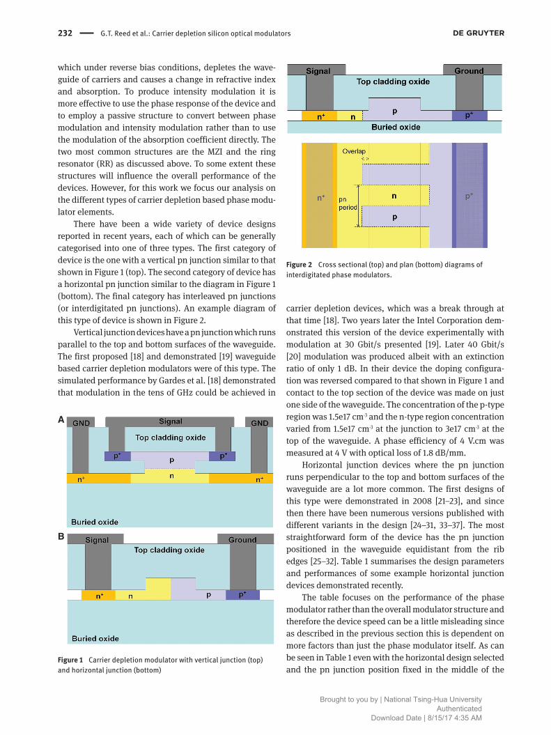
There have been a wide variety of device designs reported in recent years, each of which can be generally categorised into one of three types. The first category of device is the one with a vertical pn junction similar to that shown in Figure 1 (top). The second category of device has a horizontal pn junction similar to the diagram in Figure 1 (bottom). The final category has interleaved pn junctions (or interdigitated pn junctions). An example diagram of this type of device is shown in Figure 2.
Vertical junction devices have a pn junction which runs parallel to the top and bottom surfaces of the waveguide. The first proposed [18] and demonstrated [19] waveguide based carrier depletion modulators were of this type. The simulated performance by Gardes et al. [18] demonstrated that modulation in the tens of GHz could be achieved in
A
B
Figure 1 Carrier depletion modulator with vertical junction (top) and horizontal junction (bottom)
carrier depletion devices, which was a break through at that time [18]. Two years later the Intel Corporation dem-onstrated this version of the device experimentally with modulation at 30 Gbit/s presented [19]. Later 40 Gbit/s [20] modulation was produced albeit with an extinction ratio of only 1 dB. In their device the doping configura-tion was reversed compared to that shown in Figure 1 and contact to the top section of the device was made on just one side of the waveguide. The concentration of the p-type region was 1.5e17 cm-3 and the n-type region concentration varied from 1.5e17 cm-3 at the junction to 3e17 cm-3 at the top of the waveguide. A phase efficiency of 4 V.cm was measured at 4 V with optical loss of 1.8 dB/mm.
Horizontal junction devices where the pn junction runs perpendicular to the top and bottom surfaces of the waveguide are a lot more common. The first designs of this type were demonstrated in 2008 [21–23], and since then there have been numerous versions published with different variants in the design [24–31, 33–37]. The most straightforward form of the device has the pn junction positioned in the waveguide equidistant from the rib edges [25–32]. Table 1 summarises the design parameters and performances of some example horizontal junction devices demonstrated recently.
The table focuses on the performance of the phase modulator rather than the overall modulator structure and therefore the device speed can be a little misleading since as described in the previous section this is dependent on more factors than just the phase modulator itself. As can be seen in Table 1 even with the horizontal design selected and the pn junction position fixed in the middle of the
Figure 2 Cross sectional (top) and plan (bottom) diagrams of interdigitated phase modulators.
Brought to you by | National Tsing-Hua UniversityAuthenticated
Download Date | 8/15/17 4:35 AM

G.T. Reed et al.: Carrier depletion silicon optical modulators 233
waveguide there are still many design parameters which can be changed in order to optimise certain performance metrics. Firstly the rib waveguide geometry in terms of its height, width, slab height and sidewall angle can be varied (although in most processes the sidewall angle is fixed at around 90°). When selecting which waveguide dimensions to use there are different factors that should be considered. Firstly, the waveguide should support only single mode propagation to avoid performance degrada-tion in interferometric and resonant structures. Secondly, if polarisation independence is required without a polari-sation diversity scheme, the dimensions should be chosen to support both fundamental TE and TM modes and the effective index and optical loss for both modes should be the same [38]. The waveguide geometry also affects the confinement of the optical mode within the waveguide and therefore the degree of interaction with the region of changing refractive index (depletion region). Ultimately the optical mode confinement affects the phase efficiency of the device but also a well confined mode is likely to mean that interaction with the highly doped regions posi-tioned away from the waveguide can be reduced, benefit-ing optical loss due to absorption from free carriers. The height of the slab influences the access resistance to the pn junction and therefore the speed of the device. A thick slab therefore lends itself to a higher speed. Interaction of the optical mode with side wall roughness is also reduced and consequently scattering losses can be reduced. On the other hand a thick slab region causes high losses in waveguides bends such as those required in MZI and ring resonators.
The next consideration is the concentration and posi-tioning of the different doped regions. The distance sep-arating the waveguide rib and the highly doped regions affects the access resistance to the device and the inter-action with the optical mode. In terms of performance
this translates into device speed and optical loss. Close proximity of these regions to the waveguide will reduce access resistance to the device and therefore facilitate high speed operation, however it will also result in an increased loss. The doping concentration of the highly doped regions should be high enough to allow ohmic contacts to be formed with the device electrodes as well as providing low access resistance to the junction. The concentration of the lower dose regions influences many of the performance metrics including optical loss, phase efficiency, speed and capacitance. High doping concen-trations generally provide a reduced access resistance and higher junction capacitance. Its effect on the overall RC time constant could therefore be positive or negative depending on the design, however if the junction is cor-rectly positioned it will allow for a higher efficiency since a greater change in free carrier concentration will inter-act with the core of the optical. The down-side to a high doping concentration is the increase in absorption loss and capacitance. Therefore another trade-off exists which can also be used to tailor the device performance towards a profile of metrics as required.
Finally the design of the electrodes is a very impor-tant consideration to optimise the speed of the device. For MZI based devices coplanar waveguide electrodes (CPW) are normally employed with the diode connected between the signal track and the ground plane to one of the sides. In order to minimise reflection losses of the drive signal these electrodes should be designed to have a characteristic impedance which is matched to that of the drive equipment (usually 50 Ohms) with the effect of the pn diode on the CPW impedance taken into account. The electrodes should also be designed such that the velocity of the electrical signal is matched to the velocity of the light in the waveguide. Any velocity mismatch will mean that the drive signal will not act on the same portion of
Table 1 Comparison of horizontal pn junction modulators with the pn junction positioned in the centre of the device.
References WG width (nm)
WG height (nm)
Slab height (nm)
P conc. (cm-1)
N conc. (cm-1)
P+,N+ to WG separation (nm)
Efficiency (V.cm)
Loss (dB/mm)
Capacitance (fF/mm)
Speed (Gb/s)
[24] 480 300 80 4e18 4e18 – – 7–8 – 40[25] 500 220 90 5e17 5e17 950 1.9 (at 3V) 1.2 0.3–0.4 50[26] 500 220 90 7e17 5e17 950 3.5 (at 3V) 1a 0.27 20[27] 500 220 150 2e18 2e18 – – – – 35[28] 500 220 150 1e18 1e18 1000 1.7 (at 4V) 2.2 – 12.5[29] 500 220 100 1e18 3e18 – 1.59 (Linear) 3.2 0.84 30[30] 450 340 80 2e17 2e17 1000 1.7 (at 3V) 1.2a – 30[31] 500 220 150 1e18 1e18 1000 2 (at 3V) 2.3 0.5 10[31] 500 220 150 2e18 2e18 1000 1.2 (at 3V) 4.5 40
[32]b 400 220 70 1e18 8e17 1000 1.3 (at 0.8V) 2.3 – 26
aExcludes passive waveguide loss. bIntrinsic gap of 80 nm between p and n regions is used to reduce capacitance.
Brought to you by | National Tsing-Hua UniversityAuthenticated
Download Date | 8/15/17 4:35 AM
234 G.T. Reed et al.: Carrier depletion silicon optical modulators
light in time causing a limitation on the device speed as highlighted in the slow wave device reported by Brimont et al. [59]. RF propagation loss should be minimised. High frequency components experience greater attenuation than low frequency components meaning that the elec-trodes will have a limited bandwidth for which signals can be transmitted. A longer electrode will have a lower band-width and this means it can be difficult to achieve a large extinction ratio together with high speed due to electrode based bandwidth limitations.
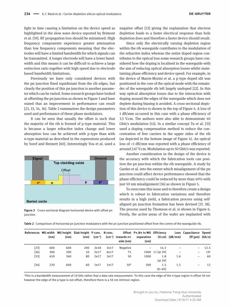
Previously we have only considered devices with the pn junction fixed equidistant from the rib edges, but clearly the position of this pn junction is another parame-ter which can be varied. Some research groups have looked at offsetting the pn junction as shown in Figure 3 and have stated that an improvement in performance can result [23, 33, 34, 36]. Table 2 summarises the design parameters used and performance of these phase modulators.
It can be seen that usually the offset is such that the majority of the rib is formed of p-type material. This is because a larger refractive index change and lower absorption loss can be achieved with p-type than with n-type material as described in the expressions produced by Soref and Bennett [60]. Interestingly You et al. used a
Figure 3 Cross-sectional diagram horizontal device with offset pn junction.
Table 2 Comparison of horizontal pn junction modulators with the pn junction positioned offset from the centre of the waveguide rib.
References WG width (nm)
WG height (nm)
Slab height (nm)
P conc. (cm-1)
N conc. (cm-1)
Offset towards n+
side (nm)
P+,N+ to WG separation
(nm)
Efficiency (V.cm)
Loss (dB/mm)
Capacitance (fF/mm)
Speed (Gb/s)
[23] 600 600 200 2e18 3e17 Negative – 14.3 – – 12.5[36] 300 200 50 2e17 6e17 75 1000 11 (at 3V) – – 19a
[33] 450 340 80 2e17 2e17 50 1000 1.8 (at 3V)
1.6 – 60
[34] 220 600 60 1e17 1e17 50b 500 1.5 (0–6V)
1.5 – 12
aThis is a bandwidth measurement of 19 GHz rather that a data rate measurement. bIn this case the edge of the n-type region is offset 50 nm however the edge of the p-type is not offset, therefore there is a 50 nm intrinsic region.
negative offset [23] giving the explanation that electron depletion leads to a faster electrical response than hole depletion does and therefore a faster device should result.
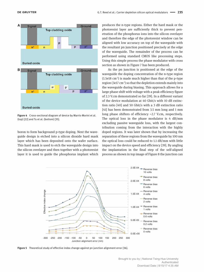
Since only the electrically varying depletion region within the rib waveguide contributes to the modulation of the refractive index whereas the entire doped region con-tributes to the optical loss some research groups have con-sidered how the doping is localised in the waveguide with the aim of reducing optical absorption losses whilst main-taining phase efficiency and device speed. For example, in the device of Marris-Morini et al. a p-type doped slit was positioned in the core of the optical mode with the remain-der of the waveguide rib left largely undoped [22]. In this way optical absorption losses due to the interaction with doping around the edges of the waveguide which does not deplete during biasing is avoided. A cross-sectional depic-tion of this device is shown in the top of Figure 4. A loss of 1 dB/mm occurred in this case with a phase efficiency of 3.5 V.cm. The authors were also able to demonstrate 40 Gbit/s modulation [43]. In a similar concept Tu et al. [35] used a doping compensation method to reduce the con-centration of free carriers in the upper sides of the rib (as depicted in the bottom image of Figure 4). An optical loss of < 1 dB/mm was reported with a phase efficiency of around 2.67 V.cm. Modulation up to 50 Gbit/s was reported.
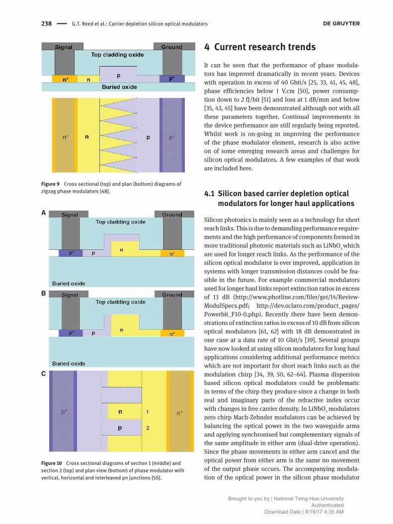
Another consideration in the design of the device is the accuracy with which the fabrication tools can posi-tion the pn junction within the rib waveguide. A study by Gardes et al. into the extent which misalignment of the pn junction could affect device performance showed that the phase efficiency could be reduced by more than 40% with just 50 nm misalignment [36] as shown in Figure 5.
To overcome this issue and to therefore create a design which is robust to fabrication variations and therefore results in a high yield, a fabrication process using self-aligned pn junction formation has been devised [37, 38]. The process used by Thomson et al. is shown in Figure 6. Firstly, the active areas of the wafer are implanted with
Brought to you by | National Tsing-Hua UniversityAuthenticated
Download Date | 8/15/17 4:35 AM
G.T. Reed et al.: Carrier depletion silicon optical modulators 235
boron to form background p-type doping. Next the wave-guide design is etched into a silicon dioxide hard mask layer which has been deposited onto the wafer surface. This hard mask is used to etch the waveguide design into the silicon overlayer and then together with a photoresist layer it is used to guide the phosphorus implant which
A
B
Figure 4 Cross-sectional diagram of device by Marris-Morini et al. (top) [22] and Tu et al. (bottom) [35].
-300 -250 -200 -100 -50 0 50Junction alignment error (nm)
Effe
ctiv
e in
dex
chan
ge
100 200 300
0.0E+00
5.0E-05
1.0E-04
1.5E-04
2.0E-04
2.5E-04Reverse bias10 volts
Reverse bias8 volts
Reverse bias6 volts
Reverse bias4 volts
Reverse bias2 volts
Reverse bias1 volts
Reverse bias0.6 volts
Reverse bias0.2 volts
Reverse bias0 volts
250150-150
Figure 5 Theoretical study of effective index change against pn junction alignment error [36].
produces the n-type regions. Either the hard mask or the photoresist layer are sufficiently thick to prevent pen-etration of the phosphorus ions into the silicon overlayer and therefore the edge of the photoresist window can be aligned with low accuracy on top of the waveguide with the resultant pn junction positioned precisely at the edge of the waveguide. The remainder of the process can be performed using standard CMOS like processing steps. Using this simple process the phase modulator with cross section as shown in Figure 7 has been produced.
As the pn junction is positioned at the edge of the waveguide the doping concentration of the n-type region (1.5e18 cm-3) is made much higher than that of the p-type region (3e17 cm-3) so that the depletion extends mainly into the waveguide during biasing. This approach allows for a large phase shift with voltage with a peak efficiency figure of 2.3 V.cm demonstrated so far [39]. In a different variant of the device modulation at 40 Gbit/s with 10 dB extinc-tion ratio [40] and 50 Gbit/s with a 3 dB extinction ratio [41] has been demonstrated from 3.5 mm long and 1 mm long phase shifters of efficiency ~2.7 V.cm, respectively. The optical loss in the phase modulator is 4 dB/mm excluding passive waveguide loss, with the largest con-tribution coming from the interaction with the highly doped regions. It was later shown that by increasing the separation of these regions from the waveguide by 100 nm the optical loss could be reduced to 1.1 dB/mm with little impact on the device speed and efficiency [39]. By angling the implantation in the final step of the self-aligned process as shown in top image of Figure 8 the junction can
Brought to you by | National Tsing-Hua UniversityAuthenticated
Download Date | 8/15/17 4:35 AM

236 G.T. Reed et al.: Carrier depletion silicon optical modulators
A
B
C
D
Figure 6 Diagram showing the self-aligned formation of the pn junction. Firstly the active region is doped p type (top left). A silicon dioxide layer is the deposited and patterned with the waveguide design (top right). This patterned silicon dioxide layer is then used as a hard mask through which to etch the waveguides (bottom left). Finally the silicon dioxide hard mask is used together with a photoresist window to define the phosphorus implantation region [37].
Figure 7 Cross sectional diagrams of phase modulators produced using the self-aligned process [37].
A
B
Figure 8 Diagram showing how ions implanted at an angle can be used to position the pn junction within the rib waveguide whilst using a self-aligned fabrication process [38].
be accurately positioned inside the waveguide. Gardes et al. used this variant of the process to produce the phase modulator shown in the bottom of Figure 8 [38].
The aim of this device was to achieve polarisation independence from a device formed with a self-aligned process. The different sections of n-type doping allowed more degrees of freedom to balance the phase efficien-cies for the fundamental TE and TM modes. Modulation at 10 Gbit/s and 40 Gbit/s was demonstrated with the same extinction ratio for both polarisations (7.3 dB and
Brought to you by | National Tsing-Hua UniversityAuthenticated
Download Date | 8/15/17 4:35 AM

G.T. Reed et al.: Carrier depletion silicon optical modulators 237
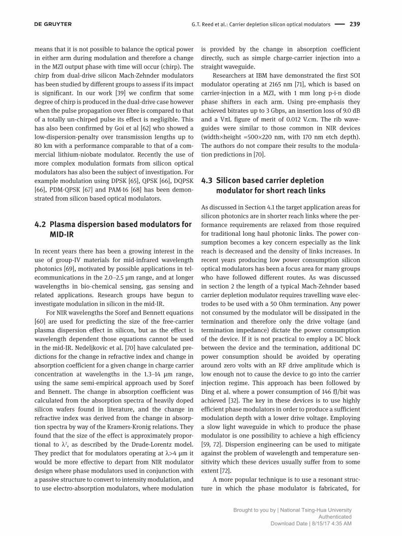
enable optimising a trade-off of efficiency and capaci-tance; however it will now be sensitive to alignment errors in the fabrication. Another way to achieve a combination of horizontal and interleaved junctions is to have a zigzag shape running along the waveguide as demonstrated in a device by Xiao et al. [48] and is depicted in Figure 9.
Their device was based in rib waveguides of height 340 nm, width 500 nm and slab height 80 nm. The doping concentrations of the p-type and n-type regions was 2e17 cm-3, whilst the separation between the highly doped regions and the rib edge was 500 nm. With this approach the authors reported a phase efficiency of 1.7 V.cm with modulation up to 44 Gbit/s. The capacitance of the phase modulator was approximately 0.7 fF/mm, however the optical loss due to the phase modulator was not reported.
As mentioned when discussing the device of Gardes et al. [38] as shown in Figure 8 (bottom) it is also possible to combine vertical and horizontal junction type devices. Such an approach has also been proposed by Spector et al. [49] and demonstrated recently by Liow et al. [42]. The device of Liow et al. was similar to that shown in Figure 8 (bottom) without the n-type region on the right hand rib edge. The authors motivation for this design was to produce a device with a vertical junction without requiring a top contact. The authors compared a horizon-tal junction device and this device achieving phase effi-ciencies of 2.56 V.cm and 1.12 V.cm, respectively, which demonstrates the advantage of this approach.
Resenberg et al. recently presented a device that combines vertical, horizontal and interleaved junctions as depicted in Figure 10 [50]. The doping densities of the p and n-type regions was 2e18 cm-3, the period of the interleaving 560 nm and the width of the p-type region on the left edge of the waveguide 100 nm. The target thickness of the p-type region at the top of the rib was 110 nm. With this device the authors achieved an impres-sive phase efficiency of 0.84 V.cm for -2 V reverse bias. A capacitance of 0.65 fF/um was reported with an optical loss of 3.5 dB/mm. Optical eye diagrams up to 40 Gbit/s were presented.
Table 3 Comparison of interleaved/interdigitated pn junction modulators.
References WG width (nm)
WG height (nm)
Slab height
(nm)
P conc. (cm-1)
N conc. (cm-1)
PN period (nm)
Overlap (nm)
P+,N+ to WG separation
(nm)
Efficiency (V.cm)
Loss (dB/mm)
Capacitance (fF/mm)
Speed (Gb/s)
[45] 450 340 80 2e17 2e17 600 0 1000 1.7 (at 3V) 1 0.65 44[46] 500 340 80 2e17 2e17 600 100 500 1.4 (at 3V) 1.7 0.34 25[47] 420 390 100 4e17 1e18 700a 0 – 3 (at 3V) – 0.2 10[31] 500 220 150 2e18 2e18 500 550 1000 0.8 (at 4V) 3.5 1.6 10
aP region is 400 nm, N region is 300 nm.
6.5 dB respectively). Recently other research groups have also used the same self-aligned angled ion implantation approach [42]. Furthermore it was also later reported that the device of Marris-Morini et al. could also be formed using a self-aligned process [43]. The device of Gardes et al. is a slightly different category of device which com-bines different pn junction types, in this case the verti-cal and horizontal pn junctions. This further category of device will be revisited later in this paper. The interdigi-tated/interleaved category of devices can also be free of alignment errors. A diagram of a typical device of this type was shown in Figure 2.
In this case the cross sectional diagram alone does not reveal the design of the junction however in the plan view the sections of p-type and n-type doping along the wave-guide can be seen. Theoretically very high modulation efficiencies can be achieved with this type of device since the relative density of depletion region in the waveguide is higher than in the other two categories of device if the period of the p-type and n-type regions is small. With this increase in depletion volume comes an increase in capaci-tance per unit length which can be detrimental in terms of device speed and power consumption. As mentioned above, tolerance to alignment errors is possible with this structure. It can be achieved if the overlap of the doped regions with the waveguide is larger than the optical mode plus the alignment accuracy of the tools used to fabricate the device. The negative impact of increasing the overlap is again the increased capacitance per unit length. The first of such devices was proposed in 2009 by Li et al. [44]. Recently there has also been some experimental demon-strations of modulation from interleaved devices as sum-marised in Table 3 [31, 45–47].
A further approach as briefly mentioned above is a junction design which encompasses a combination of ver-tical, horizontal and interleaved sections. A device with a combination of horizontal and interleaved junctions can be achieved if a negative overlap with the waveguide is used. In this case a horizontal junction exists on the sides of the interleaved doped regions. This approach may
Brought to you by | National Tsing-Hua UniversityAuthenticated
Download Date | 8/15/17 4:35 AM
238 G.T. Reed et al.: Carrier depletion silicon optical modulators
Figure 9 Cross sectional (top) and plan (bottom) diagrams of zigzag phase modulators [48].
A
B
C
Figure 10 Cross sectional diagrams of section 1 (middle) and section 2 (top) and plan view (bottom) of phase modulator with vertical, horizontal and interleaved pn junctions [50].
4 Current research trendsIt can be seen that the performance of phase modula-tors has improved dramatically in recent years. Devices with operation in excess of 40 Gbit/s [25, 33, 41, 45, 48], phase efficiencies below 1 V.cm [50], power consump-tion down to 2 fJ/bit [51] and loss at 1 dB/mm and below [35, 43, 45] have been demonstrated although not with all these parameters together. Continual improvements in the device performance are still regularly being reported. Whilst work is on-going in improving the performance of the phase modulator element, research is also active on of some emerging research areas and challenges for silicon optical modulators. A few examples of that work are included here.
4.1 Silicon based carrier depletion optical modulators for longer haul applications
Silicon photonics is mainly seen as a technology for short reach links. This is due to demanding performance require-ments and the high performance of components formed in more traditional photonic materials such as LiNbO3 which are used for longer reach links. As the performance of the silicon optical modulator is ever improved, application in systems with longer transmission distances could be fea-sible in the future. For example commercial modulators used for longer haul links report extinction ratios in excess of 13 dB (http://www.photline.com/filer/get/14/Review-ModulSpecs.pdf; http://dev.oclaro.com/product_pages/Powerbit_F10-0.php). Recently there have been demon-strations of extinction ratios in excess of 10 dB from silicon optical modulators [61, 62] with 18 dB demonstrated in one case at a data rate of 10 Gbit/s [39]. Several groups have now looked at using silicon modulators for long haul applications considering additional performance metrics which are not important for short reach links such as the modulation chirp [34, 39, 50, 62–64]. Plasma dispersion based silicon optical modulators could be problematic in terms of the chirp they produce since a change in both real and imaginary parts of the refractive index occur with changes in free carrier density. In LiNbO3 modulators zero chirp Mach-Zehnder modulators can be achieved by balancing the optical power in the two waveguide arms and applying synchronised but complementary signals of the same amplitude in either arm (dual-drive operation). Since the phase movements in either arm cancel and the optical power from either arm is the same no movement of the output phase occurs. The accompanying modula-tion of the optical power in the silicon phase modulator
Brought to you by | National Tsing-Hua UniversityAuthenticated
Download Date | 8/15/17 4:35 AM
G.T. Reed et al.: Carrier depletion silicon optical modulators 239
means that it is not possible to balance the optical power in either arm during modulation and therefore a change in the MZI output phase with time will occur (chirp). The chirp from dual-drive silicon Mach-Zehnder modulators has been studied by different groups to assess if its impact is significant. In our work [39] we confirm that some degree of chirp is produced in the dual-drive case however when the pulse propagation over fibre is compared to that of a totally un-chirped pulse its effect is negligible. This has also been confirmed by Goi et al [62] who showed a low-dispersion-penalty over transmission lengths up to 80 km with a performance comparable to that of a com-mercial lithium-niobate modulator. Recently the use of more complex modulation formats from silicon optical modulators has also been the subject of investigation. For example modulation using DPSK [65], QPSK [66], DQPSK [66], PDM-QPSK [67] and PAM-16 [68] has been demon-strated from silicon based optical modulators.
4.2 Plasma dispersion based modulators for MID-IR
In recent years there has been a growing interest in the use of group-IV materials for mid-infrared wavelength photonics [69], motivated by possible applications in tel-ecommunications in the 2.0–2.5 µm range, and at longer wavelengths in bio-chemical sensing, gas sensing and related applications. Research groups have begun to investigate modulation in silicon in the mid-IR.
For NIR wavelengths the Soref and Bennett equations [60] are used for predicting the size of the free-carrier plasma dispersion effect in silicon, but as the effect is wavelength dependent those equations cannot be used in the mid-IR. Nedeljkovic et al. [70] have calculated pre-dictions for the change in refractive index and change in absorption coefficient for a given change in charge carrier concentration at wavelengths in the 1.3–14 µm range, using the same semi-empirical approach used by Soref and Bennett. The change in absorption coefficient was calculated from the absorption spectra of heavily doped silicon wafers found in literature, and the change in refractive index was derived from the change in absorp-tion spectra by way of the Kramers-Kronig relations. They found that the size of the effect is approximately propor-tional to λ2, as described by the Drude-Lorentz model. They predict that for modulators operating at λ > 4 µm it would be more effective to depart from NIR modulator design where phase modulators used in conjunction with a passive structure to convert to intensity modulation, and to use electro-absorption modulators, where modulation
is provided by the change in absorption coefficient directly, such as simple charge-carrier injection into a straight waveguide.
Researchers at IBM have demonstrated the first SOI modulator operating at 2165 nm [71], which is based on carrier-injection in a MZI, with 1 mm long p-i-n diode phase shifters in each arm. Using pre-emphasis they achieved bitrates up to 3 Gbps, an insertion loss of 9.0 dB and a VπL figure of merit of 0.012 V.cm. The rib wave-guides were similar to those common in NIR devices (width × height = 500 × 220 nm, with 170 nm etch depth). The authors do not compare their results to the modula-tion predictions in [70].
4.3 Silicon based carrier depletion modulator for short reach links
As discussed in Section 4.1 the target application areas for silicon photonics are in shorter reach links where the per-formance requirements are relaxed from those required for traditional long haul photonic links. The power con-sumption becomes a key concern especially as the link reach is decreased and the density of links increases. In recent years producing low power consumption silicon optical modulators has been a focus area for many groups who have followed different routes. As was discussed in section 2 the length of a typical Mach-Zehnder based carrier depletion modulator requires travelling wave elec-trodes to be used with a 50 Ohm termination. Any power not consumed by the modulator will be dissipated in the termination and therefore only the drive voltage (and termination impedance) dictate the power consumption of the device. If it is not practical to employ a DC block between the device and the termination, additional DC power consumption should be avoided by operating around zero volts with an RF drive amplitude which is low enough not to cause the device to go into the carrier injection regime. This approach has been followed by Ding et al. where a power consumption of 146 fJ/bit was achieved [32]. The key in these devices is to use highly efficient phase modulators in order to produce a sufficient modulation depth with a lower drive voltage. Employing a slow light waveguide in which to produce the phase modulator is one possibility to achieve a high efficiency [59, 72]. Dispersion engineering can be used to mitigate against the problem of wavelength and temperature sen-sitivity which these devices usually suffer from to some extent [72].
A more popular technique is to use a resonant struc-ture in which the phase modulator is fabricated, for
Brought to you by | National Tsing-Hua UniversityAuthenticated
Download Date | 8/15/17 4:35 AM
240 G.T. Reed et al.: Carrier depletion silicon optical modulators
example a ring or a disk resonator. These devices produce intensity modulation by shifting the resonance wave-length on and off the input wavelength through operation of the phase modulator. Since the device can be driven as a lumped element, no termination is required and there-fore power dissipation in the termination is avoided. Several examples of low power and high speed resonant modulator have been demonstrated [24, 48, 50, 51, 73, 74]. The sensitivity of resonant based devices to fabrication variations and temperature changes require them to be actively tuned to fix the resonance wavelength as required. Athermal techniques can be used to avoid the resonance wavelength shifting with temperature [75], however this prevents thermal tuning being used to counter fabrication variations. Active tuning can be performed by incorporat-ing a heater as demonstrated by Li et al. [24] or by adding a controllable DC level to the RF drive voltage if the modu-lator is efficient enough and the tuning range required is sufficiently small [76]. An important consideration is the power consumption of the tuning element itself and there-fore the efficiency of the different heater architectures possible [77], and methods to improve the efficiency [78], have attracted increasing research interest recently.
4.4 Integration of silicon photonic modulators and detectors
One of the key cited advantages of silicon photonics is the potential to co-fabricate electronic and photonic ele-ments on the same piece of silicon [79]. Such an approach is technologically elegant and also has the potential for optimised performance since any degradation introduced by the electrical connections between different chips should be eliminated. One example of this approach is that followed by Luxtera in the fabrication of their Active optical cables (http://www.luxtera.com/). The drawback to such an approach is the high per-area cost of high per-formance electronic processing and the relative large size of the photonics elements. There is also the complexity of combining the processes for the photonic and electronic components without affecting device performance and the consideration of the required substrate in each case. A more cost effective and less complex strategy could be to separately fabricate photonic and electronic chips and then to integrate them by a wire bonding or flip chip bonding approach. The photonic chip can therefore be fabricated in a lower specification fabrication facility at lower cost.
Wire bonded integration is often referred to as an approach limited to low speed applications. The parasitic
Figure 11 Optical microscope image of the wire bonded carrier depletion modulator and CMOS driver.
inductance introduced by the bonding wire and parasitic capacitance introduced by the bonding pads may reduce the bandwidth of the link and cause an impedance dis-continuity. Within the UK Silicon Photonics programme the wire bonded approach for integrated silicon photonic transmitters and receivers operating up to 10 Gbit/s has been investigated.
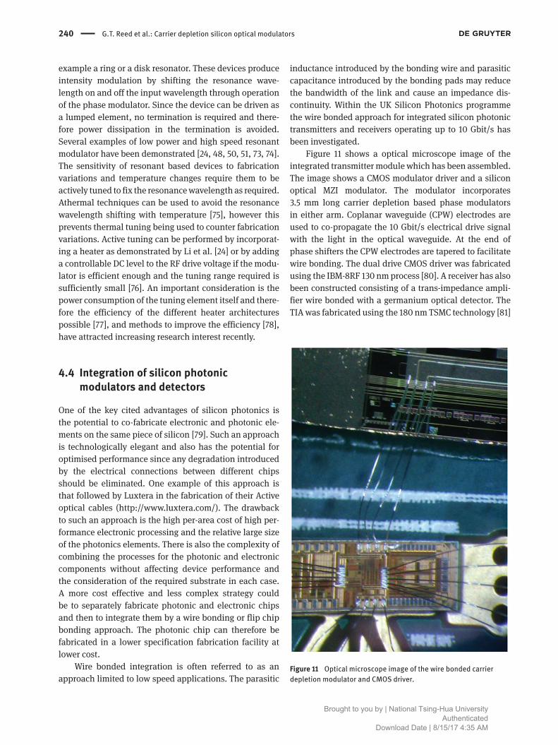
Figure 11 shows a optical microscope image of the integrated transmitter module which has been assembled. The image shows a CMOS modulator driver and a silicon optical MZI modulator. The modulator incorporates 3.5 mm long carrier depletion based phase modulators in either arm. Coplanar waveguide (CPW) electrodes are used to co-propagate the 10 Gbit/s electrical drive signal with the light in the optical waveguide. At the end of phase shifters the CPW electrodes are tapered to facilitate wire bonding. The dual drive CMOS driver was fabricated using the IBM-8RF 130 nm process [80]. A receiver has also been constructed consisting of a trans-impedance ampli-fier wire bonded with a germanium optical detector. The TIA was fabricated using the 180 nm TSMC technology [81]
Brought to you by | National Tsing-Hua UniversityAuthenticated
Download Date | 8/15/17 4:35 AM
G.T. Reed et al.: Carrier depletion silicon optical modulators 241
If the lengths of the wire bond are minimised then higher speed operation should also be possible; indeed it has been shown elsewhere that wire bond integration of silicon photonics can operate at 25 Gbit/s [82]. It should be noted in this case the limitation in the speed was set by the electronic elements and the detector which were designed to operate up to 10 Gbit/s.
5 SummaryWe have presented and provided published examples of three different configurations of carrier depletion phase modulator in silicon, as well as devices which are a mixture of these configurations. Each category of the device contains several degrees of freedom in the design which can be used to tailor a profile of performance metrics as required for a specific application. There are however some distinct advantages and disadvantages to each approach which are summarised herein.
Horizontal and interleaved junction devices can be electrically contacted via the slab regions on either side of a conventional rib waveguide, whereas the vertical junc-tion device requires contact to the top of the waveguide. This means that the use of a conventional rib waveguide is not possible in the case of a vertical junction device and that a growth process is required in the fabrication which is more complex than the implantation approaches used to form the other two configurations of device.
Interleaved devices with high p and n type doping concentrations can theoretically be fully depleted if the period of the interleaving can be made small enough. This means that highly efficient devices can be made with low absorption loss. In highly doped vertical and horizontal junction devices, carriers far from the junction remain undepleted and therefore cause high optical losses limit-ing the achievable efficiency. Doping localisation methods can be used to overcome this to some extent at the expense of fabrication complexity.
The intrinsic bandwidth of the phase modulator element is dictated by the access resistance and junction capacitance. The power consumption of the device can also be influenced by the junction capacitance depend-ing on how it is driven. The device capacitance which causes efficient modulation (or the capacitance-efficiency product) is theoretically higher (or worse) in interleaved devices since regions at the edges of the waveguide where low optical power is propagating, undergo the same depletion as at the core. Doping localisation methods can again be used to counteract this to some extent. In each
A
B
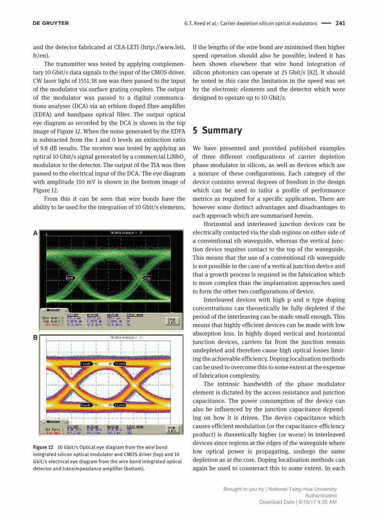
Figure 12 10 Gbit/s Optical eye diagram from the wire bond integrated silicon optical modulator and CMOS driver (top) and 10 Gbit/s electrical eye diagram from the wire bond integrated optical detector and transimpeadance amplifier (bottom).
and the detector fabricated at CEA-LETI (http://www.leti.fr/en).
The transmitter was tested by applying complemen-tary 10 Gbit/s data signals to the input of the CMOS driver. CW laser light of 1551.38 nm was then passed to the input of the modulator via surface grating couplers. The output of the modulator was passed to a digital communca-tions analyser (DCA) via an erbium doped fibre amplifier (EDFA) and bandpass optical filter. The output optical eye diagram as recorded by the DCA is shown in the top image of Figure 12. When the noise generated by the EDFA is subtracted from the 1 and 0 levels an extinction ratio of 9.8 dB results. The receiver was tested by applying an optical 10 Gbit/s signal generated by a commercial LiNbO3 modulator to the detector. The output of the TIA was then passed to the electrical input of the DCA. The eye diagram with amplitude 110 mV is shown in the bottom image of Figure 12.
From this it can be seen that wire bonds have the ability to be used for the integration of 10 Gbit/s elements.
Brought to you by | National Tsing-Hua UniversityAuthenticated
Download Date | 8/15/17 4:35 AM
242 G.T. Reed et al.: Carrier depletion silicon optical modulators
category of device the access resistance can be kept low by keeping the contacts in close proximity to the wave-guide whilst not introducing significant overlap with the optical mode which would result in high optical losses. The doping levels in the slab regions which connect to the device should also be kept sufficiently high in order to avoid high access resistance.
Vertical and interleaved junction devices have a further advantage of being inherently alignment toler-ant which simplifies fabrication; however self-aligned processes can be used to produce horizontal devices with relaxed alignment demands.
Devices which mix the different junction types can bring about further advantages, for example, by combin-ing an interleaved and horizontal junction device in way such that the pn junction is corrugated along the centre of the waveguide, the efficiency of the horizontal device can be improved.
Some excellent device performance has been dem-onstrated in the literature in recent years, with operation in excess of 40 Gbit/s, phase efficiencies below 1 V.cm, power consumption down to 2 fJ/bit and loss at 1 dB/mm and below demonstrated (although not simultaneously), confirming the carrier depletion optical modulator as an increasingly promising approach. Improving the perfor-mance of the carrier depletion modulator is however an on-going challenge. A device which combines high effi-ciency, low optical loss and high speed simultaneously is still sought after. At the same time significant research effort is devoted to the integration of the carrier depletion silicon optical modulator with electronics and other pho-tonic components.
There are several approaches and challenges for integrating electronics with photonics. Front-end inte-gration where the electronics and photonics are formed side by side on the same wafer offers the prospect of the
best performance, however the cost and complexity are high and integration density low. A back-end approach where the photonic components are formed using process temperature low enough to not damage the pre-fabricated electronics can be used, however, the perfor-mance of the photonic components formed in this way is generally inferior. A back-end wafer bonding approach can be used to affix pre-processed electronics and pho-tonics wafers, however the performance of the result-ant electrical connections between the two wafers and the yield of the bonding process require consideration. Flip chip and wire bonding can also be used, however, the parasitic capacitance and inductance introduced by these approaches could degrade and limit the perfor-mance to some extent. A 10 Gbit/s wire bond integrated silicon photonic transmitter and receiver have been pre-sented in this work. Furthermore a 25 Gbit/s wire bond integrated photonic link has been demonstrated in the literature.
Carrier depletion based silicon optical modulators remain a strong candidate for use in the growing number of short reach photonic applications and possibly even some longer reach links. Novel design features are con-tinuously being introduced which are yielding on going improvements in the device performance. With the signifi-cant worldwide resources now devoted to research in this area it is clear that there is more to come from the carrier depletion silicon optical modulator into the future.
Acknowledgements: Authors acknowledge funding from the EPSRC in the UK to support the UK Silicon Photonics project.
Received May 30, 2013; accepted November 19, 2013; previously published online December 12, 2013
References[1] Tang Y, Peters JD, Bowers JE. Over 67 GHz bandwidth hybrid
silicon electroabsorption modulator with asymmetric segmented electrode for 1.3 mm transmission. Opt Express 2012;20:11529–535.
[2] Edwards EH, Lever L, Fei ET, Kamins TI, Ikonic Z, Harris JS, Kelsall RW, Miller DAB. Low-voltage broad-band electroabsorption from thin Ge/SiGe quantum wells epitaxially grown on silicon. Opt Express 2013;21:867–76.
[3] Chaisakul P, Marris-Morini D, Rouifed M-S, Isella G, Chrastina D, Frigerio J, Le Roux X, Edmond S, Coudevylle J-R, Vivien L. Ge/SiGe multiple quantum well electro-absorption modulator. Opt Express 2012;20:3219–24.
[4] Lever L, Hu Y, Myronov M, Liu X, Owens N, Gardes FY, Marko IP, Sweeney SJ, Ikonic Z, Leadley DR, Reed GT, Kelsall RW. Modulation of the absorption coefficient at 1.3 um in Ge/SiGe multiple quantum well heterostructures on silicon. Opt Lett 2011;36:4158–60.
[5] Feng D, Liao S, Liang H, Fong J, Bijlani B, Shafiiha R, Luff BJ, Luo Y, Cunningham J, Krishnamoorthy AV, Asghari M. High speed GeSi electro-absorption modulator at 1550 nm wavelength on SOI waveguide. Opt Express 2012;20:22224–32.
[6] Ya-Ming L, Wei-Xuan H, Bu-Wen C, Zhi L, Qi-Ming W. Remarkable Franz-Keldysh Effect in Ge-on-Si p-i-n Diodes. Chin Phys Lett 2012;29:034205-1–034205-3.
Brought to you by | National Tsing-Hua UniversityAuthenticated
Download Date | 8/15/17 4:35 AM
G.T. Reed et al.: Carrier depletion silicon optical modulators 243
[7] Alloatti L, Korn D, Palmer R, Hillerkuss D, Li J, Barklund A, Dinu R, Wieland J, Fournier M, Fedeli J, Yu H, Bogaerts W, Dumon P, Baets R, Koos C, Freude W, Leuthold J. 42.7 Gbit/s electro-optic modulator in silicon technology. Opt Express 2011;19:11841–51.
[8] Gould M, Baehr-Jones T, Ding R, Huang S, Luo J, Jen AK-Y, Fedeli J-M, Fournier M, Hochberg M. Silicon-polymer hybrid slot waveguide ring-resonator modulator. Opt Express 2011;19:3952–61.
[9] Liu M, Yin X, Ulin-Avila E, Geng B, Zentgraf T, Ju L, Wang F, Zhang X. A graphene-based broadband optical modulator. Nature 2011;474:64–7.
[10] Liu M, Yin X, Zhang X. Double-layer graphene optical modulator. Nano Lett 2012;12:1482–5.
[11] Lu Z, Zhao W. Nanoscale electro-optic modulators based on graphene-slot waveguides. JOSA B 2012;29: 1490–1496.
[12] Xu C, Jin Y, Yang L, Yang J, Jiang X. Characteristics of electro-refractive modulating based on graphene-oxide-silicon waveguide. Opt Express 2012;20:22398–405.
[13] Gan X, Shiue R-J, Gao Y, Mak KF, Yao X, Li L, Szep A, Walker D Jr, Hone J, Heinz TF, Englund D. High-contrast electrooptic modulation of a photonic crystal nanocavity by electrical gating of graphene. Nano Lett 2013;13:691–6.
[14] Melikyan A, Lindenmann N, Walheim S, Leufke PM, Ulrich S, Ye J, Vincze P, Hahn H, Schimmel Th, Koos C, Freude W, Leuthold J. Surface plasmon polariton absorption modulator. Opt Express 2011;19:8855–69.
[15] Sun X, Zhou L, Li X, Hong Z, Chen J. Design and analysis of a phase modulator based on a metal-polymer-silicon hybrid plasmonic waveguide. Appl Opt 2011;50:3428–34.
[16] Sorger VJ, Lanzillotti-Kimura ND, Ma R-M, Zhang X. Ultra-compact silicon nanophotonic modulator with broadband response. Nanophotonics 2012;1:17–22.
[17] Thomas R, Ikonic Z, Kelsall RW. Electro-optic metal insulator semiconductor insulator metal Mach-Zehnder plasmonic modulator. Phot Nano Fund Appl 2012;10:183–9.
[18] Gardes F, Reed G, Emerson N, Png C. A sub-micron depletion-type photonic modulator in silicon on insulator. Opt Express 2005;13:8845–54.
[19] Liu A, Liao L, Rubin D, Nguyen H, Ciftcioglu B, Chetrit Y, Izhaky N, Paniccia M. High-speed optical modulation based on carrier depletion in a silicon waveguide. Opt Express 2007;15:660–668.
[20] Liao L, Liu A, Rubin D, Basak J, Chetrit Y, Nguyen H, Cohen R, Izhaky N, Paniccia M. 40 Gbit/s silicon optical modulator for highspeed applications. Electron Lett 2007;43:1196–1197.
[21] Spector SJ, Geis MW, Grein ME, Schulein RT, Yoon JU, Lennon DM, Gan F, Zhou G-R, Kaertner FX, Lyszczarz TM. High-speed silicon electro-optical modulator that can be operated in carrier depletion or carrier injection mode. Conference on Lasers and Electro-Optics (CLEO), San Jose, USA, 2008.
[22] Marris-Morini D, Vivien L, Fédéli J-M, Cassan E, Lyan P, Laval S. Low loss and high speed silicon optical modulation based on a lateral carrier depletion structure. Opt Express 2008;16:334–9.
[23] You J-B, Park M, Park J-W, Kim G. 12.5 Gbps optical modulation of silicon racetrack resonator based on carrier-depletion in asymmetric p-n diode. Opt Express 2008;16:18340–4.
[24] Li G, Zheng X, Thacker H, Yao J, Loo Y, Shubin I, Raj K, Cunningham JE, Krishnamoorthy AV. 40Gb/s Thermally Tunable CMOS ring Modulator. Proceedings of Group IV photonics, San Diego, USA, 2012.
[25] Dong P, Chen L, Chen Y-K. High-speed low-voltage single-drive push-pull silicon Mach-Zehnder modulators. Opt Express 2012;20:6163–9.
[26] Baehr-Jones T, Ding R, Liu Y, Ayazi A, Pinguet T, Harris NC, Streshinsky M, Lee P, Zhang Y, Lim AE-J, Liow T-Y, Teo SH-G, Lo GQ, Hochberg M. Ultralow drive voltage silicon traveling-wave modulator. Opt Express 2012;20:12014–20.
[27] Korn D, Hui Y, Hillerkuss D, Alloatti L, Mattern C, Komorowska K, Bogaerts W, Baets R, Van Campenhout J, Verheyen P, Wouters J, Moelants M, Absil P, Koos C, Freude W, Leuthold J. Detection or modulation at 35 Gbit/s with a Standard CMOS-processed Optical Waveguide. Proceedings of Conference on Lasers and Electro-Optics (CLEO), San Jose, USA, 2012.
[28] Yu H, Bogaerts W, Komorowska K, Van Campenhout J, Verheyen P, Absil PP, Baets R. 12.5 Gbits/s carrier-depletion based silicon Mach-Zehnder modulation with a 2 V driven voltage. Proceedings of the 2011 annual symposium of the IEEE Photonics Benelux Chapter, 2011, p.93–96.
[29] Kim G, Woo Park J, Kim IG, Kim S, Kim S, Lee JM, Park GS, Joo J, Jang K-S, Oh JH, Kim SA, Kim JH, Lee JY, Park JM, Kim D-W, Jeong D-K, Hwang M-S, Kim J-K, Park K-S, Chi H-K, Kim H-C, Kim D-W, Cho MH. Low-voltage high-performance silicon photonic devices and photonic integrated circuits operating up to 30 Gb/s. Opt Express 2011;19:26936–47.
[30] Li X, Xiao X, Xu H, Li Z, Chu T, Yu J, Yu Y. Highly efficient silicon Michelson interferometer modulators. IEEE Photon Technol Lett 2013;25:407–9.
[31] Yu H, Pantouvaki M, Van Campenhout J, Korn D, Komorowska K, Dumon P, Li Y, Verheyen P, Absil P, Alloatti L, Hillerkuss D, Leuthold J, Baets R, Bogaerts W. Performance tradeoff between lateral and interdigitated doping patterns for high speed carrier depletion based silicon modulators. Opt Express 2012;20:12926–38.
[32] Ding J, Chen H, Yang L, Zhang L, Ji R, Tian Y, Zhu W, Lu Y, Zhou P, Ming R, Yu M. Ultra-low-power carrier-depletion Mach-Zehnder silicon optical modulator. Opt Express 2012;20:7081–7.
[33] Xiao X, Xu H, Li X, Li Z, Chu T, Yu Y, Yu J. High-speed, low-loss silicon Mach-Zehnder modulators with doping optimization. Opt Express 2013;21:4116–25.
[34] Yi H, Long Q, Tan W, Li L, Wang X, Zhou Z. Demonstration of low power penalty of silicon Mach-Zehnder modulator in long haul transmission. Opt Express 2012;20:27562–8.
[35] Tu X, Liow T, Song J, Luo X, Fang Q, Yu M, Lo G. 50-Gb/s silicon optical modulator with traveling-wave electrodes. Opt Express 2013;21:12776–82.
[36] Gardes FY, Brimont A, Sanchis P, Rasigade G, Marris-Morini D, O’Faolain L, Dong F, Fedeli J-M, Dumon P, Vivien L, Krauss TF, Reed GT, Mart Jí. High-speed modulation of a compact silicon ring resonator based on a reverse-biased pn diode. Opt Express 2009;17:21986–91.
[37] Thomson DJ, Gardes FY, Reed GT, Milesi F, Fedeli J-M. High speed silicon optical modulator with self aligned fabrication process. Opt Express 2010;18:19064–9.
[38] Gardes FY, Thomson DJ, Emerson NG, Reed GT. 40 Gb/s silicon photonics modulator for TE and TM polarisations. Opt Express 2011;19:11804–14.
Brought to you by | National Tsing-Hua UniversityAuthenticated
Download Date | 8/15/17 4:35 AM
244 G.T. Reed et al.: Carrier depletion silicon optical modulators
[39] Thomson DJ, Gardes FY, Liu S, Porte H, Zimmermann L, Fedeli J-M, Hu Y, Nedeljkovic M, Yang X, Petropoulos P, Mashanovich GZ. High performance mach zehnder based silicon optical modulators. IEEE J Sel Top Quant 2013;19.
[40] Thomson DJ, Gardes FY, Hu Y, Mashanovich G, Fournier M, Grosse P, Fedeli J-M, Reed GT. High contrast 40Gbit/s optical modulation in silicon. Opt Express 2011;19:11507–16.
[41] Thomson DJ, Gardes FY, Fedeli J-M, Zlatanovic S, Hu Y, Kuo BP-P, Myslivets E, Alic N, Radic S, Mashanovich GZ, Reed GT. 50Gb/s silicon optical modulator. IEEE Photonic Tech L 2012;24:234–6.
[42] Liow T-Y, Song J, Tu X, Lim AE-J, Fang Q, Duan N, Yu M, Lo G-Q. Silicon optical interconnect device technologies for 40Gb/s and beyond. IEEE J Sel Top Quant 2013;19.
[43] Ziebell M, Marris-Morini D, Rasigade G, Fédéli J-M, Crozat P, Cassan E, Bouville D, Vivien L. 40 Gbit/s low-loss silicon optical modulator based on a pipin diode. Opt Express 2012;20:10591–6.
[44] Li Z-Y, Xu D-X, McKinnon RW, Janz S, Schmid JH, Cheben P, Yu J-Z. Silicon waveguide modulator based on carrier depletion in periodically interleaved PN junctions. Opt Express 2009;17:15947–58.
[45] Xu H, Xiao X, Li X, Hu Y, Li Z, Chu T, Yu Y, Yu J. High speed silicon Mach-Zehnder modulator based on interleaved PN junctions. Opt Express 2012;20:15093–9.
[46] Xiao X, Xu H, Li X, Hu Y, Xiong K, Li Z, Chu T, Yu Y, Yu J. 25 Gbit/s silicon microring modulator based on misalignment-tolerant interleaved PN junctions. Opt Express 2012;30:2507–15.
[47] Ziebell M, Marris-Morini D, Rasigade G, Crozat P, Fedeli J-M, Grosse P, Cassan E, Vivien L. Ten Gbit/s ring resonator silicon modulator based on interdigitated PN junctions. Opt Express 2011;19:14690–5.
[48] Xiao X, Li X, Hu Y, Xiong K, Li Z, Chu T, Yu J, Yu Y. 44-Gb/s silicon microring modulators based on zigzag PN junctions. IEEE Photonic Tech L 2012;24:1712–4.
[49] Spector SJ, Sorace CM, Geis MW, Geis ME, Grein ME, Yoon JU, Lyszczarz TM, Ippen EP, Kartner FX. Operation of silicon-diode-based optical modulators. IEEE J Sel Top Quant 2010;16:165–72.
[50] Rosenberg JC, Green WMJ, Assefa S, Gill DM, Barwicz T, Yang M, Shank SM, Vlasov YA. A 25Gbps silicon microring modulator based on an interleaved junction. Opt Express 2012;20: 26411–23.
[51] Zortmann WA, Lentine AL, Trotter DC, Watts MR. Low-voltage differentially-signaled modulators. Opt Express 2011;19:26017–26.
[52] Pepeljugoski P, Kash J, Doany F, Kuchta D, Schares L, Schow C, Taubenblatt M, Offrein BJ, Benner A. Low power and high density optical interconnects for future supercomputers. Proceedings of Optical Fiber Communication Conference, OThX2, San Diego, USA, 2010.
[53] Krishnamoorthy AV, Ho R > , O’Krafka B, Cunningham JE, Lexau J, Zheng X. Potentials of group IV photonics interconnects for “red-shift” computing applications. Proceedings of IEEE Group IV Photonics 2007.
[54] Barwicz T, Byun H, Gan F, Holzwarth CW, Popovic MA, Rakich PT, Watts MR, Ippen EP, Kärtner FX, Smith HI, Orcutt JS, Ram RJ, Stojanovic V, Olubuyide OO, Hoyt JL, Spector S, Geis M, Grein M, Lyszczarz T, Yoon JU. Silicon photonics for compact, energy-efficient interconnects. J Opt Networking 2007;6:63–73.
[55] Yoo SJB. Future prospects of silicon photonics in next generation communication and computing systems. Electron Lett 2009;45:584–8.
[56] Debnath K, O’Faolain L, Gardes FY, Steffan AG, Reed GT, Krauss TF. Cascaded modulator architecture for WDM applications. Opt Express 2012;20:27420–8.
[57] Guha B, Gondarenko A, Lipson M. Minimizing temperature sensitivity of silicon Mach-Zehnder interferometers. Opt Express 2010;18:1879–87.
[58] Milosevic MM, Emerson NG, Gardes FY, Chen X, Adikaari AADT, Mashanovich GZ. Athermal waveguides for optical communication wavelengths. Opt Lett 2011;36:4659–61.
[59] Brimont A, Thomson DJ, Sanchis P, Herrera J, Gardes FY, Fedeli JM, Reed GT, Marti J. High speed silicon electro-optical modulators enhanced via slow light propagation. Opt Express 2011;19:20876–85.
[60] Soref RA, Bennett BR. Electrooptical effects in silicon. IEEE J Quant Elect 1987;23:123–9.
[61] Ding J, Chen H, Yang L, Zhang L, Ji R, Tian Y, Zhu W, Lu Y, Zhou P, Min R. Low-voltage, high-extinction-ratio, Mach-Zehnder silicon optical modulator for CMOS-compatible integration. Opt Express 2012;20:3209–18.
[62] Goi K, Oda K, Kusaka H, Terada Y, Ogawa K, Liow T-Y, Tu X, Lo G-Q, Kwong D-L. 11-Gb/s 80-km transmission performance of zero-chirp silicon Mach–Zehnder modulator. Opt Express 2012;20:B350–6.
[63] Chen L, Dong P, Chen Y-K. Chirp and dispersion tolerance of a single-drive push-pull silicon modulator at 28Gb/s. IEEE Photonic Tech L 2012;24:936–8.
[64] Wei Y, Zhao Y, Yang J, Wang M, Jiang X. Chirp characteristics of silicon Mach-Zehnder modulator under small-signal modulation. IEEE J Lightwave Technol 2011;29:1011–7.
[65] Aamera M, Thomson DJ, Gutiérrez AM, Brimont A, Gardes FY, Reed GT, Fedeli JM, Hakansson A, Sanchis P. 10 Gbit/s error-free DPSK modulation using a push-pull dual-drive silicon modulator. Opt Commun 2013;304:107–10.
[66] Goi K, Kusaka H, Oka A, Terada Y, Ogawa K, Liow T-Y, Tu X, Lo G, Kwong D-L. DQPSK/QPSK modulation at 40-60 Gb/s using low-loss nested silicon Mach-Zehnder modulator. Proceedings of OFC, OW4J.4, Anaheim, USA, 2013.
[67] Dong P, Xie C, Chen L, Buhl LL, Chen Y-K. 12-Gb/s Monolithic PDM-QPSK Modulator in Silicon. Proceedings of ECOC, Postdeadline Session II (Th.3.B), Amsterdam,The Netherlands, 2012.
[68] Wu X, Dama B, Gothoskar P, Metz P, Shastri K, Sunder S, Van der Spiegel J, Wang Y, Webster M, Wilson W. A 20Gb/s NRZ/PAM-4 1V transmitter in 40nm CMOS driving a Ai-photonic modulator in 0.13um CMOS. Proceedings of ISSCC, Session 7, 7.7, San Francisco, USA, 2013.
[69] Soref R. Mid-infrared photonics in silicon and germanium. Nat Photon 2010;4:495–497.
[70] Nedeljkovic M, Soref R, Mashanovich GZ. Free-carrier electro-refraction and electro-absorption modulation predictions for silicon over the 1-14 um wavelength range. IEEE J Photon 2011;3:1171–80.
[71] Van Camp MA, Assefa S, Gill DM, Barwicz T, Rice PM, Topuria T, Green WM. Demonstration of electrooptic modulation at 2165nm using a silicon Mach-Zehnder interferometer. Opt Express 2012;20:28009–16.
Brought to you by | National Tsing-Hua UniversityAuthenticated
Download Date | 8/15/17 4:35 AM
G.T. Reed et al.: Carrier depletion silicon optical modulators 245
[72] Nguyen HC, Hashimoto S, Shinkawa M, Baba T. Sub-100mm, 40Gb/s photonics crystal silicon optical modulators. Proceedings of IEEE Group IV Photonics, San Diego, USA, 2012.
[73] Thomson DJ, Gardes FY, Cox DC, Fedeli J-M, Mashanovich GZ, Reed GT. Self-aligned silicon ring resonator optical modulator with focused ion beam error correction. J Opt Soc Am B 2013;30:445–9.
[74] Hu Y, Xiao X, Xu H, Li X, Xiong K, Li Z, Chu T, Yu Y, Yu J. High-speed silicon modulator based on cascaded microring resonators. Opt Express 2012;20:15079–85.
[75] Milosevic MM, Gardes FY, Thomson DJ, Mashanovich GZ. Temperature insensitive racetrack resonators for optical communication applications. OFC 2012, Los Angeles, USA, 4–8 March 2012.
[76] Georgas M, Leu J, Moss B, Sun C, Stojanovic V. Addressing link-level design tradeoffs for integrated photonic interconnects. IEEE Custom Integrated Circuits Conference (CICC), 2011, pp. 1–8.
[77] Masood A, Pantouvake M, Lepage G, Verheyen P, Van Campenhout J, Absil P, Van Thourhout D, Bogaerts W.
Comparison of heater architectures for thermal control of silicon photonic circuits. Proceedings of IEEE Group IV Photonics, Seoul, South Korea, 2013.
[78] Shubin I, Zheng X, Li G, Thacker H, Yao J, Guenin B, Pinguet T, Mekis A, Krishnamoorthy AV, Cunningham JE. Low power thermal tuning of SOI-CMOS photonic sturctures. Proceedings of SPIE Photonics West, San Francisco, USA, 2011.
[79] Reed GT, Knights AP. Silicon Photonics: An Introduction, Wiley: Chichester, UK, 2004.
[80] Li K, Wilson P, “An improved push-pull driver using 0.13mm CMOS” In: 2013 IEEE International Symposium on Circuits and Systems, ISCAS, Beijing, China, 2013.
[81] Hsu SH, et al. CMOS broadband amplifiers for optical communications and optical interconnects. IEEE Symposium of RF Integration Technology, Baltimore, USA, 2011.
[82] Jatar S, Malinge Y, Zhou Z, Liang H, Lioa S, Li Z, Bushyakanist C, Lee DC, Shafiiha R, Luff J, Feng D, Asghari M. Performance of parallel 4x25 Gbs transmitter and receiver fabricated on SOI platform. Proceedings of IEEE Group IV Photonics, San Diego, USA, 2012.
Brought to you by | National Tsing-Hua UniversityAuthenticated
Download Date | 8/15/17 4:35 AM