dc2464a-a/dc2464a-b: ltc3351euff hot swappable ... · cap1 caprtn capfb hs_gate isnsp_hs/ isnsm...
TRANSCRIPT

1dc2464aabf
DEMO MANUAL DC2464A-A/DC2464A-B
DESCRIPTION
LTC3351EUFFHot Swappable Supercapacitor Charger,
Backup Controller and System Monitor
Demonstration circuit 2464A-A/2464A-B is a superca-pacitor charger and backup controller with a hot swap-pable front end plus supercapacitor health and system monitoring; featuring the LTC®3351. The LTC3351 includes a buck supercapacitor charger and a backup boost controller. It has dual input hot swap FETs to con-trol the inrush current when connected and to discon-nect the input supply when an over current fault or input power loss occurs. An output ideal diode allows the
All registered trademarks and trademarks are the property of their respective owners.
supercapacitors to supply the output when VCAP is above the set backup voltage. As the capacitor stack voltage drops down to the set output voltage, the LTC3351 will operate as a boost regulator to supply the output until the energy in the supercapacitors is depleted.
Design files for this circuit board are available at http://www.linear.com/demo/DC2464A-A/A-B
TYPICAL APPLICATION
VIN
UV OUTFB
OUTFET
TGATE
SW
BGATE
ICAPVCAPCAP4
CAP3
CAP2
CAP1
CAPRTN
CAPFB
HS_GATE ISNSP_HS/ ISNSM
ICHG (STEP-DOWN) IBACKUP
VCAP < VOUT(STEP-UP)
VCAP > VOUT(DIRECTCONNECT)
VOUT
LTC3351
10FVCAP
10F
10F
10F
DC2464AAB TA01a
I2C
OV
ISNSP_CHG
5ms/DIV
DC2464AAB TA01b
IIN0.2A/DIV
VOUT2V/DIV
VIN2V/DIV
Example Hot Swap from 12V
2dc2464aabf
DEMO MANUAL DC2464A-A/DC2464A-B
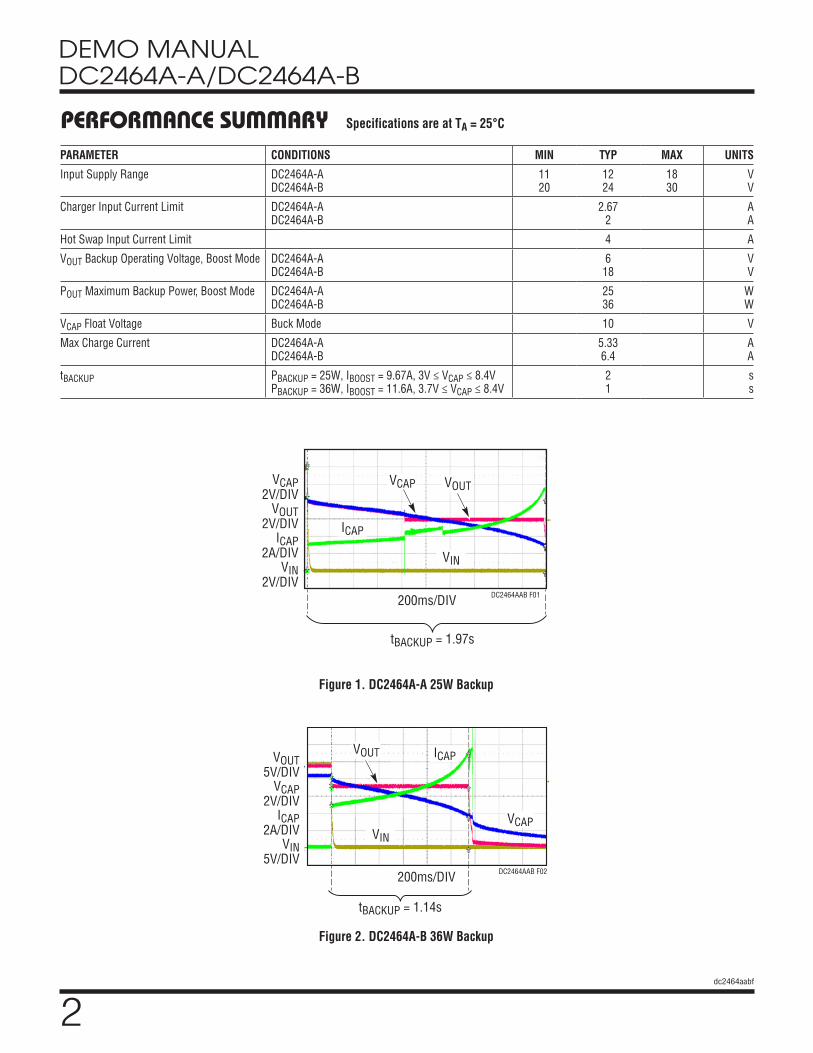
PERFORMANCE SUMMARY Specifications are at TA = 25°C
PARAMETER CONDITIONS MIN TYP MAX UNITS
Input Supply Range DC2464A-A DC2464A-B
11 20
12 24
18 30
V V
Charger Input Current Limit DC2464A-A DC2464A-B
2.67 2
A A
Hot Swap Input Current Limit 4 A
VOUT Backup Operating Voltage, Boost Mode DC2464A-A DC2464A-B
6 18
V V
POUT Maximum Backup Power, Boost Mode DC2464A-A DC2464A-B
25 36
W W
VCAP Float Voltage Buck Mode 10 V
Max Charge Current DC2464A-A DC2464A-B
5.33 6.4
A A
tBACKUP PBACKUP = 25W, IBOOST = 9.67A, 3V ≤ VCAP ≤ 8.4V PBACKUP = 36W, IBOOST = 11.6A, 3.7V ≤ VCAP ≤ 8.4V
2 1
s s
Figure 1. DC2464A-A 25W Backup
Figure 2. DC2464A-B 36W Backup
VCAP2V/DIV
VOUT2V/DIV
ICAP2A/DIV
VIN2V/DIV
200ms/DIV DC2464AAB F01
tBACKUP = 1.97s
VCAP VOUT
ICAP
VIN
200ms/DIV
VOUT5V/DIV
VCAP2V/DIV
ICAP2A/DIV
VIN5V/DIV
DC2464AAB F02
tBACKUP = 1.14s
VCAP
VOUT ICAP
VIN

3dc2464aabf
DEMO MANUAL DC2464A-A/DC2464A-B
BOARD PHOTO
Figure 3. DC2464A-A Board Photo

4dc2464aabf
DEMO MANUAL DC2464A-A/DC2464A-B
QUICK START PROCEDUREObtain and connect a DC2026C board to the DC2464A board. Use short twisted pair leads for the power connec-tions and start with the LOAD and the power supply OFF. Refer to Figures 4 and 5 for the proper measurement and equipment setup and follow the procedure below.
1. Refer to the DC2026C Quick Start Guide for QuikEval™ setup and software installation details.
2. Make sure the USB cable is connected between the computer and the DC2026C controller board.
3. Connect a 14-pin ribbon cable from the DC2026C board to the DC2464A board.
4. Set jumper JP1 on the DC2464A board to the “INTVCC” position.
5. Start the ADI QuikEval program. This program should automatically detect the presence of the LTC3351 demo board (DC2464A) and activate the appropriate GUI, as seen in Figure 9.
6. With power off, connect the appropriate supply, 0V to 20V (or 30V), 25W (or 36W) supply between the VINand GND terminals for the DC2624A-A or DC2624A-B as shown in Figure 4.
7. Turn on and set the VIN input power supply to 12V for DC2624A-A or 24V for the DC2624A-B and observe the VIN, VOUT and VCAP voltages and the input and charge currents on the GUI.
NOTE. Make sure that the input voltage does not exceed 20V for the DC2624A-A or 33V for the DC2624A-B.
8. On the LTC3351 Control Window “Charger/Control” tab, as shown in Figure 9, click on the CAP SCALE button so it displays “SMALL”. This will provide bet-ter time measurement resolution when measuring the capacitance.
9. On the LTC3351 Control Window “Cap/ESR Details” tab as shown in Figure 14, enter “2” seconds in the “cap_i_on_settling” text box. This allows the capacitor voltage time to reach the linear portion of the discharge voltage slope.
10. On the LTC3351 Control Window “Cap/ESR Details” tab as shown in Figure 14, enter “0.2” volts in the “cap_delta_v_setting” text box and then click on the Apply button on the bottom of the tab. This will pro-vide a larger dV for more accuracy.
11. On the LTC3351 Control Window, click on the CAP and ESR Measurement START button. An “In Pro-cess” indicator displays while the measurement is in process.
NOTE. Supercapacitors initially have large leakage currents which causes the capacitance measure-ment to be low. The capacitor measurements will be more accurate after the 10F capacitors have been continuously charged for more than 30 minutes.
12. Connect a constant power load box between VOUTand GND and set up to 25W for the DC2624A-A and 36W for the DC2624A-B.
13. Connect an oscilloscope probe to VIN, VOUT, VCAPand PFO. Set the oscilloscope to trigger on the fall-ing edge of PFO.
14. Remove the input power by unplugging the +VIN supply cable and observe how the output drops to the regulation point and is maintained until the energy in the supercapacitors is exhausted.
15. Turn the load off and set the oscilloscope to trigger on the rising edge of VIN.
16. Plugin the +VIN supply cable and observe how VOUT ramps up after the debounce time, showing the capacitors are charged up.
17. The LTC3351 has the ability to monitor and report on the supercapacitor and system voltages, currents, die temperature and capacitor health. See the soft-ware section and data sheet for more information.
18. The DC2464A can be modified to operate at differ-ent frequencies, operating voltages, input and boost currents. The “Hardware Config” tab allows the user to enter the appropriate changes so the GUI can report the correct measurements. See the software section for more details.

5dc2464aabf
DEMO MANUAL DC2464A-A/DC2464A-B
Figure 5. Measuring Input or Output Ripple
Figure 4. Proper Measurement Equipment Setup
QUICK START PROCEDURE

6dc2464aabf
DEMO MANUAL DC2464A-A/DC2464A-B
APPLICATION INFORMATION
The DC2464A was designed to safely connect to a pow-ered system, charge up to four supercapacitors while sup-plying a load, and provide backup power when discon-nected from the power system.
When first connected, the LTC3351, hot swap controller waits for the debounce period set by the CSS1 capacitor, about 26ms for this board. VOUT will then ramp up at a dV/dt set also set by CSS1. After the VIN is within the VINGD range then the charger will charge the capacitors to the set float voltage.
The capacitors are initially charged to about 84% of the full-scale, the default CAPFB setting. As the capacitors age decreasing their backup capability, the capacitor stack
voltage can be increased the backup time as needed. This can increase the usage life of the capacitors.
When the power is disconnected, the LTC3351 quickly switches from charge mode to backup mode. If the set backup voltage is set below the VCAP voltage, the output power is initially powered from VCAP thru the output ideal diode as shown in Figure 8. As VCAP approaches the set VOUT backup voltage then the backup boost regulator starts to hold VOUT at the set voltage.
If the set VOUT backup voltage is set higher than VOUT, the backup boost regulator starts immediately to pump up and maintain the VOUT to the set backup voltage.
Figure 6. Charger Efficiency Figure 7. Boost Efficiency
IIN(MAX) = 2AIOUT = 0A
0 1.7 3.4 5.1 6.8 8.50
20
40
60
80
100
EFFI
CIEN
CY (%
)
DC2464AAB F06
VIN = 12VVIN = 24VVIN = 35V
VCAP (V) IOUT (A)
EFFI
CIEN
CY (%
)
0.001 0.01 0.1 1 10
VCAP = 2VVCAP = 3VVCAP = 4V
DC2464AAB F07
VOUT = 10V
0
10
20
30
40
50
60
70
80
90
100
Figure 8. Charge and Discharge Cycle
VIN
VCAPVOUT
IIN
ICAP
IOUT
HOTPLUG
DEBOUNCE CC CHARGINGCP CHARGING
CV CHARGING AND BALANCING
POWER FAILUREIDEAL DIODE BACKUP
TIME (NOT TO SCALE)
0
0
VOLT
AGE
CURR
ENT
INRUSHCONTROL
BOOST BACKUP
DC2464AAB F08
7dc2464aabf
DEMO MANUAL DC2464A-A/DC2464A-B
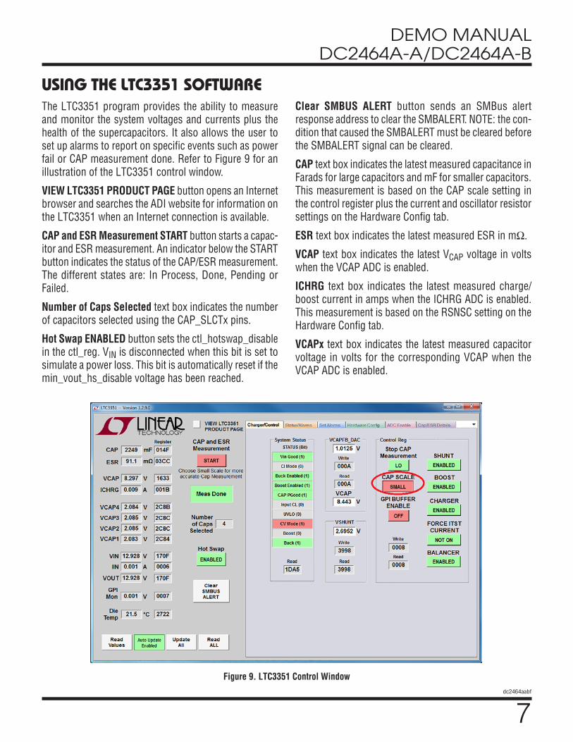
Figure 9. LTC3351 Control Window
The LTC3351 program provides the ability to measure and monitor the system voltages and currents plus the health of the supercapacitors. It also allows the user to set up alarms to report on specific events such as power fail or CAP measurement done. Refer to Figure 9 for an illustration of the LTC3351 control window.
VIEW LTC3351 PRODUCT PAGE button opens an Internet browser and searches the ADI website for information on the LTC3351 when an Internet connection is available.
CAP and ESR Measurement START button starts a capac-itor and ESR measurement. An indicator below the START button indicates the status of the CAP/ESR measurement. The different states are: In Process, Done, Pending or Failed.
Number of Caps Selected text box indicates the number of capacitors selected using the CAP_SLCTx pins.
Hot Swap ENABLED button sets the ctl_hotswap_disable in the ctl_reg. VIN is disconnected when this bit is set to simulate a power loss. This bit is automatically reset if the min_vout_hs_disable voltage has been reached.
USING THE LTC3351 SOFTWAREClear SMBUS ALERT button sends an SMBus alert response address to clear the SMBALERT. NOTE: the con-dition that caused the SMBALERT must be cleared before the SMBALERT signal can be cleared.
CAP text box indicates the latest measured capacitance in Farads for large capacitors and mF for smaller capacitors. This measurement is based on the CAP scale setting in the control register plus the current and oscillator resistor settings on the Hardware Config tab.
ESR text box indicates the latest measured ESR in mΩ.
VCAP text box indicates the latest VCAP voltage in volts when the VCAP ADC is enabled.
ICHRG text box indicates the latest measured charge/ boost current in amps when the ICHRG ADC is enabled. This measurement is based on the RSNSC setting on the Hardware Config tab.
VCAPx text box indicates the latest measured capacitor voltage in volts for the corresponding VCAP when the VCAP ADC is enabled.

8dc2464aabf
DEMO MANUAL DC2464A-A/DC2464A-B
USING THE LTC3351 SOFTWAREVIN text box indicates the latest measured input voltage in volts when the VIN ADC is enabled.
IIN text box indicates the latest measured input current in amps when the IIN ADC is enabled. This measurement is based on the RSNSI setting on the Hardware Config tab.
VOUT text box indicates the latest measured VOUT in volts when the VOUT text box is enabled.
GPI Mon text box indicates the latest measured GPI voltage in volts when the GPI Mon ADC is enabled. An internal buf-fer can be enabled for measuring high impedance inputs.
Die Temp text box displays the latest internally measured die temperature in °C when the Die Temp ADC is enabled.
Register text boxes displays the associated register val-ues in hexadecimal format.
Read Values button causes the LTC3351 to read the ADC measured values. This is useful when the LTC3351 GUI “Auto Update” is disabled.
Auto Update Enabled/Disabled button causes the LTC3351 to read the LTC3351 registers periodically and writes to any register changed when enabled. The Read Values, Read All, or Update All buttons can be used instead to update the registers when in the disabled state.
Read All button causes the LTC3351 to read the LTC3351 registers. This is useful when the LTC3351 GUI Auto Update is disabled.
Charger Control Tab
The Charger Control tab contains the indicators and con-trols for the capacitor charger and monitor plus the GPI buffer enable as shown in Figure 9.
System Status STATUS (Bit) indicates when the associ-ated chrg_status register bits are set. See the data sheet for more information on these bits.
System Status Read text box displays the last read sys_status register value in hexadecimal format.
VCAPFB_DAC text box allows the user to set the CAPFB reference voltage from 0.6375V to 1.2V in 37.5mV incre-ments. The value in the text box is rounded to the nearest mV. The VCAP text box is also updated with the calculated
value of the CAPFB reverence voltage and the resistor network entered on the Hardware Config tab.
VCAPFB_DAC Write text box displays the value that will be or has been written to the vcapfb_dac register in hexa-decimal format.
VCAPFB_DAC Read text box displays the last value read from the vcapfb_dac register in hexadecimal format.
VCAP text box allows the user to set the VCAP float volt- age within the limits of the CAPFB reference voltage and the CAPFB resistor network on the Hardware Config tab. The value in the text box is rounded to the nearest mV. The VCAPFB_DAC text box is also updated with the calculated value using the CAPFB resistor network entered on the Hardware Config tab.
VSHUNT text box allows the user to set the shunt regula-tor voltage up to 5.5V. When set below 3.6V, the charger will limit current and the active shunts will shunt current to prevent this voltage from being exceeded. When pro-grammed above 3.6V no current will be shunted, however, the charge current will be reduced as described. As a capacitor voltage nears this level, the charge current will be reduced. The shunt voltage will be reset to the default value of 2.6952 every time INTVCC is restored.
VSHUNT Write text box displays the value that will be or has been written to the VSHUNT register in hexadecimal format.
VSHUNT Read text box displays the last value read from the VSHUNT register in hexadecimal format.
Stop CAP Measurement sets the ctl_stop_cap_esr_meas bit in the ctl_reg register. This will cause any CAP/ESR measurement in process to stop. This bit will reset when the measurement has ceased.
CAP SCALE button sets the cap scale from large scale, default scale for larger capacitors, to small scale for smaller capacitors like used on the DC2464A. The reso-lution is increased by 100× in small scale.
GPI BUFFER ENABLE button sets the ctl_gpi_buffer_en bit when enabling the GPI input buffer. When the GPI BUF-FER ENABLE is off then the GPI input is measured without the input buffer.

9dc2464aabf
DEMO MANUAL DC2464A-A/DC2464A-B
SHUNT ENABLED button disables the shunt regulator when set. When not set, the shunt regulator will prevent the caps from charging over the set VSHUNT voltage.
BOOST ENABLED button disables the boost regulator when set. When not set, the boost regulator will operate as required in backup mode.
CHARGER ENABLED button disables the charger when set. When not set, charger will operate when possible.
FORCE ITST CURRENT button turns on the internal capacitor discharge current source. This can be used to discharge the capacitors or to manually measure the capacitors. NOTE: this does not disable the charger. Select the CHARGER ENABLED button to disable the charger.
BALANCER ENABLED button disables the capacitor bal-ancers when set. When not set, the balancers will balance the capacitors about 10mV of each other.
Control Reg Write text box displays the value that will be or has been written to the ctl_reg register in hexadecimal format.
USING THE LTC3351 SOFTWAREControl Reg Read text box displays the last value read from the ctl_reg register in hexadecimal format.
Status/Alarms Tab
The Status/Alarms tab contains the indicators for the monitor_status_reg and alarm_reg bits plus control but-tons for the Monitor Status Mask, Alarm Mask and Alarm Clear bits as shown in Figure 10.
Monitor Status Status (Bit) indicate when the associated monintor_status_reg bits are set. See the data sheet for more information on these bits.
Monitor Status Read text box displays the last read monitor_status_reg value in hexadecimal format.
Mask Monitor Status buttons will allow the rising edge of the associated monitor status bit to trigger the SMBALERT when the mask bit is set to 1.
Mask Monitor Write text box displays the value that will be or has been written to the monitor_status_mask_reg in hexadecimal format.
Figure 10. Status/Alarms Tab

10dc2464aabf
DEMO MANUAL DC2464A-A/DC2464A-B
Mask Monitor Read text box displays the last read monitor_status_mask_reg value in hexadecimal format.
ALARM (Bit) indicate when the associated alarm_reg bits are set. See the data sheet for more information on these bits.
Alarm Read text box displays the last read alarm_reg value in hexadecimal format.
Mask Alarm buttons will allow the associated alarm bit to trigger the SMBALERT when the mask bit is set to 1.
Mask Alarm Write text box displays the value that will be or has been written to the alarm_mask_reg in hexa-decimal format.
Mask Alarm Read text box displays the last alarm_mask_reg value in hexadecimal format.
Clear Alarm buttons will cause the associated alarm to clear when the alarm condition no longer exists by writing a “0” in the appropriate alarm_reg bit.
Set Alarms Tab
The Set Alarms tab contains text boxes to allow the user to set specific levels for each alarm register as shown in Figure 11. Each alarm has an associated Write text box to display the value that will be or has been written to the associated register in hexadecimal format. Each alarm also has an associated Read text box which displays the last read contents of the associated register in hexadeci-mal format.
VIN/VOUT/VCAP/CAP/GPI UV Alarm text boxes allow the user to enter a voltage that will trigger an alarm when the associated voltage drops below the entered voltage value and the associated alarm mask bit is set.
VIN/VOUT/VCAP/CAP/GPI OV Alarm text boxes allow the user to enter a voltage that will trigger an alarm when the associated voltage rises above the entered voltage value and the associated alarm mask bit is set.
USING THE LTC3351 SOFTWARE
Figure 11. Set Alarms Tab

11dc2464aabf
DEMO MANUAL DC2464A-A/DC2464A-B
IIN OC alarm text boxes allow the user to enter a current or the voltage across the sense resistor that will trigger an alarm when the input current increase above the entered value and the mask_alarm_iin_oc bit is set.
CAP LO alarm text box allows the user to enter a capaci-tance based on the current ctl_cap_scale setting in the ctl_reg. A CAP LO alarm will be triggered if the measured capacitance is lower than the entered value and the mask_alarm_cap_lo bit is set.
ESR HI alarm text box allows the user to enter an ESR value based on the RSNSC resistor value entered in the Hardware Config tab. An ESR HI alarm will be triggered if the measured ESR is higher than the entered value and the mask_alarm_esr_hi bit is set.
ICHRG UC alarm text boxes allow the user to enter a cur-rent or the voltage across the sense resistor that will trig-ger an alarm when the charge current decreases below the entered value and the mask_alarm_ichrg_uc bit is set.
Die Temp Cold alarm text box allows the user to enter a die temperature in °C that will trigger an alarm when the temperature decreases below the entered value and the mask_alarm_dtemp_cold bit is set.
Die Temp Hot alarm text box allows the user to enter a die temperature in °C that will trigger an alarm when the temperature increases above the entered value and the mask_alarm_dtemp_hot bit is set.
Apply button writes to the alarm registers and reads the values back from the LTC3351.
Cancel button changes all the entered values that have not yet been written to the LTC3351 back to their previ-ous values.
Restore Defaults button changes the LTC3351 alarm registers back to the default values determined from the GUI. This does not set the alarm to the LTC3351’s default settings of 0x0000.
Hardware Config Tab
The Hardware Config tab, shown in Figure 12, contains text boxes to allow the user to enter the values to con-figure the necessary resistors to match the configuration of the demo board. These values are used by the GUI to calculate measured CAP and ESR values, display input/charge currents and max VCAP voltage for a given refer-ence setting. These values are also used in the Set Alarm tab text boxes.
USING THE LTC3351 SOFTWARE
Figure 12. Hardware Config Tab

12dc2464aabf
DEMO MANUAL DC2464A-A/DC2464A-B
RITST text box allows the user to enter the RITST resis-tor in Ω. The calculated test current setting is displayed in mA.
REXT text box allows the user to enter the external load resistance, R28 and R29, added in Ω if any. Enter 0 if there is not any external loading and OPEN will be displayed in the text box. See the Using Large Capacitor section for more details.
RT text box allows the user to enter the RT resistor in kΩ. The calculated oscillator setting is displayed in kHz.
Total RBalance text box allows the user to enter the equivalent total balance resistance in Ω if any for capaci-tance stacks or packs that have external balancing. Enter 0 if there is not any external balancing and OPEN will be displayed in the text box.
RSNSI text box allows the user to enter the RSNSI resis-tor in mΩ. The calculated input current limit setting is displayed in Amps. This is the total resistance sensed between the isnsp_chg and the ISNSM pin. If R8 is popu-lated and R1 is not, then it should be the value of the RSNSH1 resistor. If R8 is not populated and R1 is, then it should be the total of the RSNSI1 and RSNSH1 resistors.
RSNSC text box allows the user to enter the RSNSC resis-tor in mΩ. The calculated maximum charge current set-ting is displayed in Amps.
VCAP Resistor Settings text boxes allow the user to enter the CAPFB resistor divider network in kΩ. The calculated maximum VCAP set point is displayed in volts.
CAP1 Voltage Divider text boxes allow the user to enter the CAP1 resistor divider network in kΩ if used. This could be used if a large capacitor stack or a capacitor pack with its own balancing was used. The displayed CAP1 voltage is calculated from the maximum VCAP voltage. Enter 0 in the CAP1 Voltage Divider RTop and RBot text boxes then OPEN will be displayed in both text boxes.
ADC Enable Tab
The ADC Enable tab contains control buttons to enable the ADC measurements when charging and when operating on backup power. It also contains a text box to configure the delay for each ADC measurement, and configurable voltage thresholds which require specific ADC measure-ments to be enabled.
USING THE LTC3351 SOFTWARE
Figure 13. ADC Enable Tab

13dc2464aabf
DEMO MANUAL DC2464A-A/DC2464A-B
Each control has an associated Write text box to display the value that will be or has been written to the associated register in hexadecimal format. Each control also has an associated Read text box which displays the last read contents of the associated register in hexadecimal format.
At the bottom of the tab are buttons to Apply, Cancel, and Restore Defaults for the settings on this tab.
ENABLES. These buttons enable and disable the ADC measurements in the LTC3351. Press the button to toggle the measurement between 1 (on) and 0 (off).
DELAYS. Set these text boxes to configure the wait time between ADC measurements in ms.
MIN CAP BOOST VOLTAGE. The Min Cap Boost set-ting requires the applicable VCAPx measurements to be enabled during backup. It controls the minimum capacitor cell voltage at which the LTC3351 will continue powering VOUT with the boost regulator.
MIN VOUT HS DISABLE VOLTAGE. The VOUT to match GUI Disable setting requires the VOUT measurement to
be enabled in backup. It controls the minimum voltage at which the LTC3351 will disable Hot Swap and return to charging the capacitors when VIN power becomes avail-able. The ctl_hotswap_disable bit is also cleared when this voltage is reached.
APPLY/CANCEL/RESTORE DEFAULTS. These buttons write and read the settings between the LTC3351 and the GUI. Apply will write the selected settings to the LTC3351, Cancel will restore the GUI to the settings in the LTC3351, and Restore Defaults will return both the GUI and the LTC3351 to the defaults for the IC.
CAP/ESR Details Tab
The CAP/ESR Details tab contains text boxes to configure the measurements of the capacitance and ESR for each capacitor. When a CAP/ESR measurement is performed, intermediate calculations are reported in the registers displayed on this tab which can be used to evaluate the readings. The individual capacitance and ESR for each capacitor are calculated and reported at the bottom of the page.
USING THE LTC3351 SOFTWARE
Figure 14. Cap/ESR Details Tab

14dc2464aabf
DEMO MANUAL DC2464A-A/DC2464A-B
Each control has an associated Write text box to display the value that will be or has been written to the associated register in hexadecimal format. Each control also has an associated Read text box which displays the last read contents of the associated register in hexadecimal format.
ESR DETAILS. The text boxes at the top of this section contain the ESR and capacitor measurement settling times which can be adjusted for better measurement accuracy. The esr_i_override current is used to force a specific charge current to use when performing the ESR measurement. This is used if the next_esr_i current plus the load will cause the part to reach the input current limit and create an inaccurate ESR measurement. Refer to the ESR and Capacitor Measurement section of the LTC3351 data sheet for more information on the capacitor and ESR measurement.
When the ESR measurement is started and allowed to complete, the intermediate calculations performed for the final reported ESR value are displayed in this section.
CAP DETAILS. The cap_delta_v_setting text box at the top of this section contains the voltage difference used to perform the capacitance measurement. The voltage will be charged to 1.25* cap_delta_v_setting, turn on the discharge current source, wait for the cap_i_on_settling time and then measure the capacitor stack voltage. The LTC3351 then measures the time it takes to discharge the cap_delta_v_setting voltage. When the measurement has completed the charger turns on and maintains the float voltage.
USING THE LTC3351 SOFTWAREWhen the capacitance measurement is started and allowed to complete, the voltage difference per capacitor is displayed in this section.
CAP/ESR PER CAPACITOR. The Capacitance and ESR for VCAP1/VCAP2/VCAP3/VCAP4 are reported at the bottom of the tab, using the reported details in the other sections.
APPLY/CANCEL/RESTORE DEFAULTS. These buttons write and read the settings between the LTC3351 and the GUI. Apply will write the selected settings to the LTC3351, Cancel will restore the GUI to the settings in the LTC3351, and Restore Defaults will return both the GUI and the LTC3351 to the defaults for the IC.
The DC2464A standard configuration is designed for supercapacitors of 200F or less. The standard configura-tion measures the time it takes to discharge the capacitor stack by 100mV at 33.6mA to calculate the capacitance. Larger supercapacitors have larger leakage currents, some over a milliamp, causing an inaccuracy in the capacitive measurement. To increase the measurement accuracy, the capacitor test current can be increased by loading the capacitor stack with external resistors, R50 and R51, during the measurement. The low threshold N-MOSFET, M6, is controlled by the ITST pin which turns on the load when needed.

15dc2464aabf
DEMO MANUAL DC2464A-A/DC2464A-B
USING LARGE CAPACITORS
Figure 15. External Test Current
Figure 16. High Current Shunting
ISHUNT =VSHUNT
2 • RSHUNT+
VSHUNT
RSHUNT(OPT)
Optional External Test Current Larger capacitors also take longer to balance. If one capacitor is far enough off balance that it reaches the shunt voltage before the capacitor stack is fully charged. The charge current effectively is reduced to the shunt cur-rent until the capacitor stack is fully charged. The standard DC2464A board is set up for a 500mA maximum shunt current. This current can be increased by turning on exter-nal shunt resistors across each capacitor, R42 thru R49. The controlling FETs, M7 thru M10, are turned on from the voltage drop across the corresponding shunt resis-tor when the shunt regulator turns on. The 2.7Ω shunt resistors between the supercapacitor and the CAPx pin as shown in Figure 16 can be used to provide a larger shunt current.When using this circuit, the test current will be the origi-
nal ITST circuit current plus an additional current due to the capacitor stack voltage across the resistor. This requires a modified equation for converting meas_cap to capacitance.
This equation for small scale is:
C =–56 • 10–9 • Rt • meas _ cap
R • ln 1–∆ VCAP
1.2V •R
RTST+ VCAP
CAP4
R50100Ω2W
R51100Ω2W
ITST
Si2374DS
M11
DC2464AAB F15
CAP4
R422.7Ω2W
R432.7Ω2W
GCAP4
SiA436DJ
M7
DC2464AAB F16
CAP3

16dc2464aabf
DEMO MANUAL DC2464A-A/DC2464A-B
PARTS LIST – DC2464A-AITEM QTY REFERENCE PART DESCRIPTION MANUFACTURER/PART NUMBER
Required Circuit Components
1 1 C1 CAP., 1µF, X5R, 50V, 10%, 0603, AEC-Q200 TDK, CGA3E3X5R1H105K080AB
2 1 C2 CAP., 120pF, C0G, 50V, 5%, 0402 MURATA, GRM1555C1H121JA01D
3 6 C6−C9, C15, C16 CAP., 47µF, X5R, 25V, 20%, 1206 TDK, C3216X5R1E476M160AC
4 2 C13, C14 CAP., 2.2µF, X5R, 25V, 10%, 0402 TDK, C1005X5R1E225K050BC
5 1 C17 CAP., 4.7µF, X5R, 16V, 10%, 0603 AVX, 0603YD475KAT2A
6 4 C18, C25, C26, CBST1 CAP., 0.1µF, X7R, 16V, 10%, 0402 AVX, 0402YC104KAT2A
7 4 C19, C20, C22, C23 CAP., 22µF, X5R, 16V, 20%, 0805 TDK, C2012X5R1C226M125AC
8 1 C21 CAP., 1µF, X5R, 16V, 10%, 0402 TAIYO YUDEN, EMK105BJ105KV-F
9 1 C28 CAP., 0.01µF, X7R, 16V, 10%, 0402 AVX, 0402YC103KAT2A
10 4 CAP1-CAP4 CAP., 10F, ULTRA, 2.7V, –10/+20%, THT, RADIAL NESSCAP, ESHSR-0010C0-002R7
11 1 CSS1 CAP. CER., 0.022µF, 100V, X7R, 0603 TDK, C1608X7R2A223K080AA
12 1 CTIMER1 CAP., 0.033µF, X5R, 16V, 10%, 0402, AEC-Q200 TDK, CGA2B2X5R1C333K050BA
13 1 D1 DIODE, TVS, 18V, 600W, SMB DIODES INC., SMBJ18A-13-F
14 1 DBST1 DIODE, GP SWITCHING, 80V, 125mA, SOD523, AEC-Q10X DIODES INC., 1N4448HWT-7
15 1 L1 IND., 3.3µH, PWR., 20%, 10A, 21.45mΩ, SMD 7.5mm × 7.5mm, AEC-Q200
COILCRAFT, XAL7030-332MEB
16 2 M1, M2 XSTR., MOSFET, N-CH, 25V, 23A, TSDSON-8 INFINEON, BSZ018NE2LSATMA1
17 2 M3, M4 XSTR., MOSFET, N-CH, 25V, 12A, TSDSON-8 INFINEON, BSZ060NE2LSATMA1
18 1 M5 XSTR., MOSFET, N-CH, 20V, 16A, PowerPAK 1212-8 VISHAY, SiS438DN-T1-GE3
19 2 R4, R5 RES., 10Ω, 5%, 1/16W, 0402 VISHAY, CRCW040210R0JNED
20 1 R11 RES., 649k, 1%, 1/16W, 0402 NIC, NRC04F6493TRF
21 1 R12 RES., 162k, 1%, 1/16W, 0402 VISHAY, CRCW0402162KFKED
22 1 R14 RES., 100Ω, 1%, 1/16W, 0402 NIC, NRC04F1000TRF
23 1 R15 RES., 665k, 1%, 1/16W, 0402 NIC, NRC04F6653TRF
24 1 R17 RES., 33.2k, 1%, 1/16W, 0402 VISHAY, CRCW040233K2FKED
25 1 R18 RES., AEC-Q200, 49.9k, 1%, 1/16W, 0402 PANASONIC, ERJ2RKF4992X
26 5 R25, R27, R29, R30, R32 RES., ANTI-SURGE, AEC-Q200, 2.7Ω, 5%, 1/2W, 0805 PANASONIC, ERJ-P6WJ2R7V
27 1 R35 RES., 866k, 1%, 1/16W, 0402 NIC, NRC04F8663TRF
28 1 R36 RES., 118k,1%, 1/16W, 0402 NIC, NRC04F1183TRF
29 1 RITST1 RES., AEC-Q200, 35.7Ω, 1%, 1/16W, 0402 VISHAY, CRCW040235R7FKED
30 1 RSNSC1 RES., SENSE, 0.006Ω, 1%, 1W, 1206 (0612) SUSUMU
31 1 RSNSH1 RES., SENSE, 0.012Ω, 1%, 1W, 1206 (0612) SUSUMU, PRL1632-R012-F-T1
32 1 RSNSI1 RES., SENSE, AEC-Q200, 0.004Ω, 1%, 1.5W, 1206 (0612) SUSUMU, KRL3216E-C-R004-F-T1
33 1 RT1 RES., 71.5k, 1%, 1/16W, 0402 NIC, NRC04F7152TRF
34 1 U1 IC, HOT SWAPPABLE SUPERCAPACITOR CHARGER BACKUP CONTROLLER AND SYSTEM MONITOR
ADI, LTC3351EUFF#PBF

17dc2464aabf
DEMO MANUAL DC2464A-A/DC2464A-B
ITEM QTY REFERENCE PART DESCRIPTION MANUFACTURER/PART NUMBER
Additional Demo Board Circuit Components
35 0 C3, C4 DNP
36 0 C5, C12, C27 DNP
37 0 C10, C11 DNP
38 0 C24 DNP
39 1 C29 CAP., 0.1µF, X7R, 16V, 10%, 0402 AVX, 0402YC104KAT2A
40 0 D2 DNP
41 2 D3, D4 LED, GREEN, MILKY WHITE DIFF., 0603 SMD, 565nm LUMEX, SML-LX0603GW-TR
42 1 D5 LED, SUPER RED, MILKY WHITE DIFF., 0603 SMD, 660nm LUMEX, SML-LX0603SRW-TR
43 2 D6, D7 DNP
44 0 M5 DNP
45 0 M6 DNP
46 0 M7-M10 DNP
47 0 M11 DNP
48 1 Q1 XSTR., MOSFET, DUAL N-CH, 20V, 1.3A, SOT-363 VISHAY, Si1922EDH-T1-GE3
49 0 R1 DNP
50 2 R2, R3 RES., 1Ω,1%, 1/16W, 0402 VISHAY, CRCW04021R00FKED
51 2 R6, R31 RES., 20Ω,1%, 1/16W, 0402 NIC, NRC04F20R0TRF
52 0 R7, R9, R22, R24 DNP
53 0 R8 DNP
54 6 R8, R10, R13, R16, R28, R52 RES., 0Ω,1/16W, 0402 ROHM, MCR01MZPJ000
55 2 R19, R20 RES., 5.1k, 5%, 1/16W, 0402 NIC, NRC04J512TRF
56 4 R21, R23, R37, R38 RES., 100k, 5%, 1/16W, 0402 YAGEO, RC0402JR-07100KL
57 3 R26, R33, R34 RES., 1MΩ, 5%, 1/16W, 0402 YAGEO, RC0402JR-071ML
58 3 R39-R41 RES., 1k, 5%, 1/16W, 0402 NIC, NRC04J102TRF
59 0 R42-R51 DNP
60 1 U2 IC, MEMORY, EEPROM, 2Kb (256 × 8), TSSOP-8, 400kHz MICROCHIP, 24LC025-I/ST
61 0 Z1 DNP
Hardware for Demo Board Only
62 11 E1-E6, E8, E10-E12, E17 TEST POINT, TURRET, 0.094", MTG. HOLE MILL-MAX, 2501-2-00-80-00-00-07-0
63 6 E7, E9, E13-E16 TEST POINT, TURRET, 0.064", MTG. HOLE MILL-MAX, 2308-2-00-80-00-00-07-0
64 1 J1 CONN., HDR., MALE, 2mm × 7mm, 2mm, THT, VERT, SHROUDED
MOLEX, 87831-1420
65 1 JP1 CONN., HDR, MALE, 1mm × 3mm, 2mm, THT, STR WURTH ELEKTRONIK, 62000311121
PARTS LIST – DC2464A-A

18dc2464aabf
DEMO MANUAL DC2464A-A/DC2464A-B
PARTS LIST – DC2464A-BITEM QTY REFERENCE PART DESCRIPTION MANUFACTURER/PART NUMBER
Required Circuit Components
1 1 C1 CAP., 1µF, X5R, 50V, 10%, 0603, AEC-Q200 TDK, CGA3E3X5R1H105K080AB
2 1 C2 CAP., 120pF, C0G, 50V, 5%, 0402 MURATA, GRM1555C1H121JA01D
3 6 C6-C9, C15, C16 CAP., 10µF, X5R, 50V, 10%, 1206 MURATA, GRM31CR61H106KA12L
4 2 C10, C11 CAP., 33µF, ALUM., 50V, 20%, SMD 6.3mm × 7.7mm, AEC-Q200
PANASONIC, EEHZA1H330XP
5 2 C13, C14 CAP., 0.1µF, X7R, 50V, 10%, 0402 MURATA, GRM155R71H104KE14D
6 1 C17 CAP., 4.7µF, X5R, 16V, 10%, 0603 AVX, 0603YD475KAT2A
7 4 C18, C25, C26, CBST1 CAP., 0.1µF, X7R, 16V, 10%, 0402 AVX, 0402YC104KAT2A
8 4 C19, C20, C22, C23 CAP., 22µF, X5R, 16V, 20%, 0805 TDK, C2012X5R1C226M125AC
9 1 C21 CAP., 1µF, X5R, 16V, 10%, 0402 TAIYO YUDEN, EMK105BJ105KV-F
10 1 C24 CAP., 220pF, C0G, 50V, 5%, 0402 AVX, 04025A221JAT2A
11 1 C28 CAP., 1200pF, X7R, 50V, 10%, 0402 AVX, 04025C122KAT2A
12 4 CAP1-CAP4 CAP., 10F, ULTRA, 2.7V, –10/+20%, THT, RADIAL NESSCAP, ESHSR-0010C0-002R7
13 1 CSS1 CAP. CER., 0.022µF, 100V, X7R, 0603 TDK, C1608X7R2A223K080AA
14 1 CTIMER1 CAP., 0.033µF, X5R, 16V, 10%, 0402, AEC-Q200 TDK, CGA2B2X5R1C333K050BA
15 1 D1 DIODE, TVS, UNI-DIR., 30V, 600W, SMB LITTELFUSE, SMBJ30A
16 1 DBST1 DIODE, GP SWITCHING, 80V, 125mA, SOD523, AEC-Q10X DIODES INC., 1N4448HWT-7
17 1 L1 IND., 6.8µH, PWR, 20%, 9.2A, 19.62mΩ, SMD 7.2mm × 7.5mm, AEC-Q200
COILCRAFT, XAL7070-682MEB
18 4 M1-M4 XSTR., N-CH, 40V, 17.6A, PowerPAK 1212-8 VISHAY, SIS434DN-T1-GE3
19 2 R4, R5 RES., 10Ω, 5%, 1/16W, 0402 VISHAY, CRCW040210R0JNED
20 1 R11 RES., 649k, 1%, 1/16W, 0402 NIC, NRC04F6493TRF
21 1 R12 RES., 46.4k, 1%, 1/16W, 0402 VISHAY, CRCW040246K4FKED
22 1 R14 RES., 100Ω, 1%, 1/16W, 0402 NIC, NRC04F1000TRF
23 1 R15 RES., 665k, 1%, 1/16W, 0402 NIC, NRC04F6653TRF
24 1 R17 RES., 14.3k, 1%, 1/16W, 0402 VISHAY, CRCW040214K3FKED
25 1 R18 RES., AEC-Q200, 28k, 1%, 1/16W, 0402 VISHAY, CRCW040228K0FKED
26 5 R25, R27, R29, R30, R32 RES., ANTI-SURGE, AEC-Q200, 2.7Ω, 5%, 1/2W, 0805 PANASONIC, ERJ-P6WJ2R7V
27 1 R35 RES., 866k, 1%, 1/16W, 0402 NIC, NRC04F8663TRF
28 1 R36 RES., 118k, 1%, 1/16W, 0402 NIC, NRC04F1183TRF
29 1 RITST1 RES., AEC-Q200, 35.7Ω, 1%, 1/16W, 0402 VISHAY, CRCW040235R7FKED
30 1 RSNSC1 RES., SENSE, 0.005Ω, 1%, 1W, 1206 (0612) SUSUMU, PRL1632-R005-F-T1
31 1 RSNSH1 RES., SENSE, 0.012Ω, 1%, 1W, 1206 (0612) SUSUMU, PRL1632-R012-F-T1
32 1 RSNSI1 RES., SENSE, AEC-Q200, 0.004Ω, 1%, 1.5W, 1206 (0612) SUSUMU, KRL3216E-C-R004-F-T1
33 1 RT1 RES., 107k, 1%, 1/16W, 0402 VISHAY, CRCW0402107KFKED
34 1 U1 IC, HOT SWAPPABLE SUPERCAPACITOR CHARGER BACKUP CONTROLLER AND SYSTEM MONITOR
ADI, LTC3351EUFF#PBF

19dc2464aabf
DEMO MANUAL DC2464A-A/DC2464A-B
PARTS LIST – DC2464A-BITEM QTY REFERENCE PART DESCRIPTION MANUFACTURER/PART NUMBER
Additional Demo Board Circuit Components
35 0 C3, C4 DNP
36 0 C5,C12,C27 DNP
37 1 C29 CAP., 0.1µF, X7R, 16V, 10%, 0402 AVX, 0402YC104KAT2A
38 1 D2 DIODE, SCHOTTKY, 40V, 10A, PowerDI5 DIODES INC., PDS1040L-13
39 2 D3, D4 LED, GREEN, MILKY WHITE DIFF., 0603 SMD, 565nm LUMEX, SML-LX0603GW-TR
40 1 D5 LED, SUPER RED, MILKY WHITE DIFF., 0603 SMD, 660nm LUMEX, SML-LX0603SRW-TR
41 3 D6-D8 DIODE, SBR, 40V, 1A, SOD123F DIODES INC., 1N5819HW1-7-F
42 0 M5 DNP
43 0 M6 DNP
44 0 M7-M10 DNP
45 0 M11 DNP
46 1 Q1 XSTR., MOSFET, DUAL N-CH, 20V, 1.3A, SOT-363 VISHAY, Si1922EDH-T1-GE3
47 3 R1-R3 RES., 1Ω, 1%, 1/16W, 0402 VISHAY, CRCW04021R00FKED
48 2 R6, R31 RES., 20Ω, 1%, 1/16W, 0402 NIC, NRC04F20R0TRF
49 0 R7, R9, R22, R24 DNP
50 0 R8 DNP
51 4 R10, R13, R16, R28 RES., 0Ω, 1/16W, 0402 ROHM, MCR01MZPJ000
52 2 R19, R20 RES., 5.1k, 5%, 1/16W, 0402 NIC, NRC04J512TRF
53 4 R21, R23, R37, R38 RES., 100k, 5%, 1/16W, 0402 YAGEO, RC0402JR-07100KL
54 3 R26, R33, R34 RES., 1MΩ, 5%, 1/16W, 0402 YAGEO, RC0402JR-071ML
55 3 R39-R41 RES., 1k, 5%, 1/16W, 0402 NIC, NRC04J102TRF
56 0 R42-R51 DNP
57 1 R52 RES., 10Ω, 5%, 1/16W, 0402 VISHAY, CRCW040210R0JNED
58 1 U2 IC, MEMORY, EEPROM, 2KB (256 × 8), TSSOP-8, 400kHz MICROCHIP, 24LC025-I/ST
Hardware-For Demo Board Only
59 11 E1-E6, E8, E10-E12, E17 TEST POINT, TURRET, 0.094", MTG. HOLE MILL-MAX, 2501-2-00-80-00-00-07-0
60 6 E7, E9, E13-E16 TEST POINT, TURRET, 0.064", MTG. HOLE MILL-MAX, 2308-2-00-80-00-00-07-0
61 1 J1 CONN., HDR., MALE, 2 × 7, 2mm, THT, VERT, SHROUDED MOLEX, 87831-1420
62 1 JP1 CONN., HDR, MALE, 1 × 3, 2mm, THT, STR WURTH ELEKTRONIK, 62000311121

20dc2464aabf
DEMO MANUAL DC2464A-A/DC2464A-B
SCHEMATIC DIAGRAM – DC2464A-A5 5
4 4
3 3
2 2
1 1
DD
CC
BB
AA
PCA
ADDI
TION
AL P
ARTS
J1-V
CC
OPTI
ONAL
EXT
ERNA
L SH
UNT
CURR
ENT
INTV
CC
PULL
- UP
POW
ER
OPTI
ONAL
EXT
ERNA
LTE
ST C
URRE
NT
THE
SCL
AND
SDA
PULL
-DOW
N RE
SIST
ORS
ARE
FOR
STA
ND-A
LONE
OPE
RATI
ON O
NLY
WHE
N TH
E I2
C BU
S IS
NOT
USE
D.
REVI
SION
HIS
TORY
ECO
REV
DESC
RIPT
ION
APPR
OVED
DATE
-4
PROD
UCTI
ONMM
10-1
7-17
HOT
SWAP
PABL
E SU
PERC
APAC
ITOR
CHA
RGER
BAC
KUP
CONT
ROLL
ER A
ND S
YSTE
M MO
NITO
R
SDA
SCL
VIN*
GND
GPI
GND
VOUT
*
GND
VCAP
GND
CAP3
CAP2
CAP1
GND
SMBA
LERT
VING
DCA
PGD
SMBA
LERT
CAPG
D
VING
D
GND
FSW
*IT
ST=3
3.6m
A
CAP4
VOUT
BAC
KUP
20V
- 30V
24V
NOM
INAL
DC24
64A
- B
DC24
64A
- A
18V
36W
11V
- 18V
12V
NOM
INAL
6V 2
5W
VERS
ION
TABL
E*
SKU
#VI
N/VO
UTFS
W
750k
Hz
500k
Hz-
2A C
HARG
ER IN
PUT
CURR
ENT
LIMI
T4A
CIR
CUIT
BRE
AKER
INST
ALLE
D
INPU
T CU
RREN
T LI
MIT
NOT
INST
ALLE
DIN
STAL
LED
NOT
INST
ALLE
D
R1R8
2.67A
CHA
RGER
INPU
T CU
RREN
T LI
MIT
4A C
IRCU
IT B
REAK
ER
ALTE
RNAT
E HO
TSW
APCO
MPON
ENTS
C3 C4 R9 OPTI
ONAL
INPU
TSH
ORTC
IRCU
ITPR
OTEC
TION
COMP
ONEN
TS
R1-R
3R5
2D2 D6
-D8
5V M
AX
VCC
VCC
INTV
CC
INTV
CC
DATE
:
IC N
O.
SHEE
TOF
TITL
E: D
EMO
CIRC
UIT
SCHE
MAT
IC,
APPR
OVAL
SPC
B DE
S.
APP
ENG.
Fax:
(408
)434
-050
7
Milp
itas,
CA 95
035
Phon
e: (4
08)4
32-1
900
1630
McC
arth
y Blvd
.
LTC
Conf
iden
tial-F
or C
usto
mer
Use
Onl
y
CUST
OMER
NOT
ICE
LINE
AR T
ECHN
OLOG
Y HA
S MA
DE A
BES
T EF
FORT
TO
DESI
GN A
CIRC
UIT
THAT
MEE
TS C
USTO
MER-
SUPP
LIED
SPE
CIFI
CATI
ONS;
HOW
EVER
, IT R
EMAI
NS T
HE C
USTO
MER'
S RE
SPON
SIBI
LITY
TO
VERI
FY P
ROPE
R AN
D RE
LIAB
LE O
PERA
TION
IN T
HE A
CTUA
LAP
PLIC
ATIO
N. C
OMPO
NENT
SUB
STIT
UTIO
N AN
D PR
INTE
DCI
RCUI
T BO
ARD
LAYO
UT M
AY S
IGNI
FICA
NTLY
AFF
ECT
CIRC
UIT
PERF
ORMA
NCE
OR R
ELIA
BILI
TY. C
ONTA
CT L
INEA
RTE
CHNO
LOGY
APP
LICA
TION
S EN
GINE
ERIN
G FO
R AS
SIST
ANCE
.
THIS
CIR
CUIT
IS P
ROPR
IETA
RY T
O LI
NEAR
TEC
HNOL
OGY
AND
SUPP
LIED
FOR
USE
WIT
H LI
NEAR
TEC
HNOL
OGY
PART
S.
SCAL
E =
NONE
www.
linea
r.com
SIZE
:SK
U NO
.SC
HEM
ATIC
NO.
AND
REV
ISIO
N:PC
A AS
S'Y
DWG:
11
NC MM
LTC3351
710-
DC24
64A_
REV
0470
5-DC
2464
A_RE
V04
Thur
sday
, Oct
ober
19, 2
017
8.5x1
1
DC24
64A
ADA
TE:
IC N
O.
SHEE
TOF
TITL
E: D
EMO
CIRC
UIT
SCHE
MAT
IC,
APPR
OVAL
SPC
B DE
S.
APP
ENG.
Fax:
(408
)434
-050
7
Milp
itas,
CA 95
035
Phon
e: (4
08)4
32-1
900
1630
McC
arth
y Blvd
.
LTC
Conf
iden
tial-F
or C
usto
mer
Use
Onl
y
CUST
OMER
NOT
ICE
LINE
AR T
ECHN
OLOG
Y HA
S MA
DE A
BES
T EF
FORT
TO
DESI
GN A
CIRC
UIT
THAT
MEE
TS C
USTO
MER-
SUPP
LIED
SPE
CIFI
CATI
ONS;
HOW
EVER
, IT R
EMAI
NS T
HE C
USTO
MER'
S RE
SPON
SIBI
LITY
TO
VERI
FY P
ROPE
R AN
D RE
LIAB
LE O
PERA
TION
IN T
HE A
CTUA
LAP
PLIC
ATIO
N. C
OMPO
NENT
SUB
STIT
UTIO
N AN
D PR
INTE
DCI
RCUI
T BO
ARD
LAYO
UT M
AY S
IGNI
FICA
NTLY
AFF
ECT
CIRC
UIT
PERF
ORMA
NCE
OR R
ELIA
BILI
TY. C
ONTA
CT L
INEA
RTE
CHNO
LOGY
APP
LICA
TION
S EN
GINE
ERIN
G FO
R AS
SIST
ANCE
.
THIS
CIR
CUIT
IS P
ROPR
IETA
RY T
O LI
NEAR
TEC
HNOL
OGY
AND
SUPP
LIED
FOR
USE
WIT
H LI
NEAR
TEC
HNOL
OGY
PART
S.
SCAL
E =
NONE
www.
linea
r.com
SIZE
:SK
U NO
.SC
HEM
ATIC
NO.
AND
REV
ISIO
N:PC
A AS
S'Y
DWG:
11
NC MM
LTC3351
710-
DC24
64A_
REV
0470
5-DC
2464
A_RE
V04
Thur
sday
, Oct
ober
19, 2
017
8.5x1
1
DC24
64A
A
R36
118k
U1 LTC3
351-
UFF
VCAP
24
UV42
CAP_
SLCT
12
VINGD 3
PGND 45
CFP
20
CFN
21
BST
29
BGAT
E30
SMBALERT 6
CAPFB 9
OUTF
B10
SGND
11
RT12
HSGATE40
ISNSP_CHG36
ISNSP_HS37
SRC39
VIN
41
SCL
4
SDA
5
ICAP
25
VCC2
P526
SW27
TGAT
E28
CAP2
17
CAP3
18
CAP4
19
CAP_
SLCT
01
VCAP
P522
OUTF
ET23
INTV
CC32
DRVC
C31
CAPGD 7
VC8
GPI
13
ITST
14
CAPRTN 15
CAP1
16
CTIMER 44
OV43
RETRYB34VOUT33
CSS38
ISNSM35
E15E5
RT1
71.5
k
J1
HDR.
VUNR
EG1
GND
3
MIS
O5
MOS
I/SDA
7
EESD
A9
EESC
L11
GND
13
VCCI
O2
SCK/
SCL
4CS
6
GND
8
EEVC
C10
EEGN
D12
GPIO
14
R37
100k
+CA
P310
F
R47
DNP
R2 1
E4
R19
5.1k
D1
R21
100k
C24
DNP
D2DN
P
21
3
R17
33.2
k
TPB1
MP1
STAN
DOFF
, NYL
ON, S
NAP-
ON,0
.375
"
R3 1
R11
649k
C7 47uF
+C1
0DN
P
R35
866k
Q1A
SI19
22ED
H-T1
-GE3
2
6 1
M2
BSZ0
18NE
2LS
TP2
R40
1k
R12
162k
R32 2.7
R27
2.7
D6
DNP
E6
R41
1k
C28
0.01
uF
L1 3.3u
H
CTIM
ER1
0.03
3uF
C6 47uF
C5 DNP
CBST
10.
1uF
E13
Q1B
SI19
22ED
H-T1
-GE3
5
3 4
PCB1
PCB,
DC2
464A
REV0
4
+C1
1DN
P
E1
MP4
STAN
DOFF
, NYL
ON, S
NAP-
ON,0
.375
"
D5
C20
22uF
R52
0
R46
DNP
CSS1
0.02
2uF
TPB2
C17
4.7u
F
+CA
P110
F
STNC
L1TO
OL, S
TENC
IL, 7
00-D
C246
4ARE
V04
C21
1uFC3 DN
P
D3
C1 1uF
C9 47uF
C22
22uF
R4 10
E10
R23
100k
R43
DNP
R31
20
R38
100k
M1
BSZ0
18NE
2LS
R18
49.9
k
E14
C25
0.1u
F
R6 20
R30
2.7
C23
22uF
C16
47uF
C2 120p
F
M7
DNP
R28
0
RSNS
H1
0.01
2
R25
2.7
R51
DNP
TP1
RSNS
C1
0.00
6
E11
C14
2.2u
F
R26
1M
E8
R7 DNP
R13
0
MP3
STAN
DOFF
, NYL
ON, S
NAP-
ON,0
.375
"
R1DN
P
D4
R45
DNP
RSNS
I1
0.00
4
M4
BSZ0
60NE
2LS
E16
R50
DNP M
11
DNP
RITS
T1 35.7
E2
R34
1M
M6 DN
P
M8
DNP
D7
DNP
M5
SIS4
38DN
-T1-
GE3
R20
5.1k
R42
DNP
+CA
P210
FE1
2
C29
0.1u
F
R16 0
M9
DNP
TPA1
R10
0C4
DNP
R15
665k
R39
1k
E9
C26
0.1u
F
D8
DNP
R14
100
R22
DNP
M3
BSZ0
60NE
2LS
C12
DNP
R44
DNP
R49
DNP
JP1
R29
2.7
Z1 DNP
5.6V
R48
DNP
R9 DNP
+CA
P410
F
MP2
STAN
DOFF
, NYL
ON, S
NAP-
ON,0
.375
"
R33 1M
E3R8 0
M10
DNP
E17
C8 47uF
R24
DNP
LB1
LABE
L
DBST
1
1N4448HWT-7
TPA2
C18
0.1u
F
U2
24LC
025-
I/ST
A01
A12
A23
VSS 4
SDA
5SC
L6
WP
7
VCC8
C13
2.2u
F
R5 10
C27
DNP
C19
22uF
C15
47uF
E7
GCAP
4GC
AP3
GCAP
2GC
AP1
CAP2
CAP1
CAP4
CAP4
CAP3
CAP2
CAP3
CAP1
GCAP
1
GCAP
2
GCAP
3
GCAP
4
ITST
ITST
CAP4
CAP1
CAP3
CAP2

21dc2464aabf
DEMO MANUAL DC2464A-A/DC2464A-B
Information furnished by Analog Devices is believed to be accurate and reliable. However, no responsibility is assumed by Analog Devices for its use, nor for any infringements of patents or other rights of third parties that may result from its use. Specifications subject to change without notice. No license is granted by implication or otherwise under any patent or patent rights of Analog Devices.
SCHEMATIC DIAGRAM – DC2464A-B5 5
4 4
3 3
2 2
1 1
DD
CC
BB
AA
PCA
ADDI
TION
AL P
ARTS
J1-V
CC
OPTI
ONAL
EXT
ERNA
L SH
UNT
CURR
ENT
INTV
CC
PULL
- UP
POW
ER
OPTI
ONAL
EXT
ERNA
LTE
ST C
URRE
NT
THE
SCL
AND
SDA
PULL
-DOW
N RE
SIST
ORS
ARE
FOR
STA
ND-A
LONE
OPE
RATI
ON O
NLY
WHE
N TH
E I2
C BU
S IS
NOT
USE
D.
REVI
SION
HIS
TORY
ECO
REV
DESC
RIPT
ION
APPR
OVED
DATE
-4
PROD
UCTI
ONMM
10-1
7-17
HOT
SWAP
PABL
E SU
PERC
APAC
ITOR
CHA
RGER
BAC
KUP
CONT
ROLL
ER A
ND S
YSTE
M MO
NITO
R
SDA
SCL
VIN*
GND
GPI
GND
VOUT
*
GND
VCAP
GND
CAP3
CAP2
CAP1
GND
SMBA
LERT
VING
DCA
PGD
SMBA
LERT
CAPG
D
VING
D
GND
FSW
*IT
ST=3
3.6m
A
CAP4
VOUT
BAC
KUP
20V
- 30V
24V
NOM
INAL
DC24
64A
- B
DC24
64A
- A
18V
36W
11V
- 18V
12V
NOM
INAL
6V 2
5W
VERS
ION
TABL
E*
SKU
#VI
N/VO
UTFS
W
750k
Hz
500k
Hz-
2A C
HARG
ER IN
PUT
CURR
ENT
LIMI
T4A
CIR
CUIT
BRE
AKER
INST
ALLE
D
INPU
T CU
RREN
T LI
MIT
NOT
INST
ALLE
DIN
STAL
LED
NOT
INST
ALLE
D
R1R8
2.67A
CHA
RGER
INPU
T CU
RREN
T LI
MIT
4A C
IRCU
IT B
REAK
ER
ALTE
RNAT
E HO
TSW
APCO
MPON
ENTS
C3 C4 R9 OPTI
ONAL
INPU
TSH
ORTC
IRCU
ITPR
OTEC
TION
COMP
ONEN
TS
R1-R
3R5
2D2 D6
-D8
5V M
AX
VCC
VCC
INTV
CC
INTV
CC
DATE
:
IC N
O.
SHEE
TOF
TITL
E: D
EMO
CIRC
UIT
SCHE
MAT
IC,
APPR
OVAL
SPC
B DE
S.
APP
ENG.
Fax:
(408
)434
-050
7
Milp
itas,
CA 95
035
Phon
e: (4
08)4
32-1
900
1630
McC
arth
y Blvd
.
LTC
Conf
iden
tial-F
or C
usto
mer
Use
Onl
y
CUST
OMER
NOT
ICE
LINE
AR T
ECHN
OLOG
Y HA
S MA
DE A
BES
T EF
FORT
TO
DESI
GN A
CIRC
UIT
THAT
MEE
TS C
USTO
MER-
SUPP
LIED
SPE
CIFI
CATI
ONS;
HOW
EVER
, IT R
EMAI
NS T
HE C
USTO
MER'
S RE
SPON
SIBI
LITY
TO
VERI
FY P
ROPE
R AN
D RE
LIAB
LE O
PERA
TION
IN T
HE A
CTUA
LAP
PLIC
ATIO
N. C
OMPO
NENT
SUB
STIT
UTIO
N AN
D PR
INTE
DCI
RCUI
T BO
ARD
LAYO
UT M
AY S
IGNI
FICA
NTLY
AFF
ECT
CIRC
UIT
PERF
ORMA
NCE
OR R
ELIA
BILI
TY. C
ONTA
CT L
INEA
RTE
CHNO
LOGY
APP
LICA
TION
S EN
GINE
ERIN
G FO
R AS
SIST
ANCE
.
THIS
CIR
CUIT
IS P
ROPR
IETA
RY T
O LI
NEAR
TEC
HNOL
OGY
AND
SUPP
LIED
FOR
USE
WIT
H LI
NEAR
TEC
HNOL
OGY
PART
S.
SCAL
E =
NONE
www.
linea
r.com
SIZE
:SK
U NO
.SC
HEM
ATIC
NO.
AND
REV
ISIO
N:PC
A AS
S'Y
DWG:
11
NC MM
LTC3351
710-
DC24
64A_
REV
0470
5-DC
2464
A_RE
V04
Thur
sday
, Oct
ober
19, 2
017
8.5x1
1
DC24
64A
BDA
TE:
IC N
O.
SHEE
TOF
TITL
E: D
EMO
CIRC
UIT
SCHE
MAT
IC,
APPR
OVAL
SPC
B DE
S.
APP
ENG.
Fax:
(408
)434
-050
7
Milp
itas,
CA 95
035
Phon
e: (4
08)4
32-1
900
1630
McC
arth
y Blvd
.
LTC
Conf
iden
tial-F
or C
usto
mer
Use
Onl
y
CUST
OMER
NOT
ICE
LINE
AR T
ECHN
OLOG
Y HA
S MA
DE A
BES
T EF
FORT
TO
DESI
GN A
CIRC
UIT
THAT
MEE
TS C
USTO
MER-
SUPP
LIED
SPE
CIFI
CATI
ONS;
HOW
EVER
, IT R
EMAI
NS T
HE C
USTO
MER'
S RE
SPON
SIBI
LITY
TO
VERI
FY P
ROPE
R AN
D RE
LIAB
LE O
PERA
TION
IN T
HE A
CTUA
LAP
PLIC
ATIO
N. C
OMPO
NENT
SUB
STIT
UTIO
N AN
D PR
INTE
DCI
RCUI
T BO
ARD
LAYO
UT M
AY S
IGNI
FICA
NTLY
AFF
ECT
CIRC
UIT
PERF
ORMA
NCE
OR R
ELIA
BILI
TY. C
ONTA
CT L
INEA
RTE
CHNO
LOGY
APP
LICA
TION
S EN
GINE
ERIN
G FO
R AS
SIST
ANCE
.
THIS
CIR
CUIT
IS P
ROPR
IETA
RY T
O LI
NEAR
TEC
HNOL
OGY
AND
SUPP
LIED
FOR
USE
WIT
H LI
NEAR
TEC
HNOL
OGY
PART
S.
SCAL
E =
NONE
www.
linea
r.com
SIZE
:SK
U NO
.SC
HEM
ATIC
NO.
AND
REV
ISIO
N:PC
A AS
S'Y
DWG:
11
NC MM
LTC3351
710-
DC24
64A_
REV
0470
5-DC
2464
A_RE
V04
Thur
sday
, Oct
ober
19, 2
017
8.5x1
1
DC24
64A
B
R36
118k
U1 LTC3
351-
UFF
VCAP
24
UV42
CAP_
SLCT
12
VINGD 3
PGND 45
CFP
20
CFN
21
BST
29
BGAT
E30
SMBALERT 6
CAPFB 9
OUTF
B10
SGND
11
RT12
HSGATE40
ISNSP_CHG36
ISNSP_HS37
SRC39
VIN
41
SCL
4
SDA
5
ICAP
25
VCC2
P526
SW27
TGAT
E28
CAP2
17
CAP3
18
CAP4
19
CAP_
SLCT
01
VCAP
P522
OUTF
ET23
INTV
CC32
DRVC
C31
CAPGD 7
VC8
GPI
13
ITST
14
CAPRTN 15
CAP1
16
CTIMER 44
OV43
RETRYB34VOUT33
CSS38
ISNSM35
E15E5
RT1
107k
J1
HDR.
VUNR
EG1
GND
3
MIS
O5
MOS
I/SDA
7
EESD
A9
EESC
L11
GND
13
VCCI
O2
SCK/
SCL
4CS
6
GND
8
EEVC
C10
EEGN
D12
GPIO
14
R37
100k
+CA
P310
F
R47
DNP
R2 1
E4
R19
5.1k
D1
R21
100k
C24
220p
F
D2PD
S104
0L-1
3
21
3
R17
14.3
k
TPB1
MP1
STAN
DOFF
, NYL
ON, S
NAP-
ON,0
.375
"
R3 1
R11
649k
C7 10uF
+C1
033
uF
R35
866k
Q1A
SI19
22ED
H-T1
-GE3
2
6 1
M2
SIS4
34DN
-T1-
GE3
TP2
R40
1k
R12
46.4
k
R32 2.7
R27
2.7
D6
1N58
19HW
1-7-
F
E6
R41
1k
C28
1200
pF
L1 6.8u
H
CTIM
ER1
0.03
3uF
C6 10uF
C5 DNP
CBST
10.
1uF
E13
Q1B
SI19
22ED
H-T1
-GE3
5
3 4
PCB1
PCB,
DC2
464A
REV0
4
+C1
133
uF
E1
MP4
STAN
DOFF
, NYL
ON, S
NAP-
ON,0
.375
"
D5
C20
22uF
R52
10
R46
DNP
CSS1
0.02
2uF
TPB2
C17
4.7u
F
+CA
P110
F
STNC
L1TO
OL, S
TENC
IL, 7
00-D
C246
4ARE
V04
C21
1uFC3 DN
P
D3
C1 1uF
C9 10uF
C22
22uF
R4 10
E10
R23
100k
R43
DNP
R31
20
R38
100k
M1
SIS4
34DN
-T1-
GE3
R18
28k
E14
C25
0.1u
F
R6 20
R30
2.7
C23
22uF
C16
10uF
C2 120p
F
M7
DNP
R28
0
RSNS
H1
0.01
2
R25
2.7
R51
DNP
TP1
RSNS
C1
0.00
5
E11
C14
0.1u
F
R26
1M
E8
R7 DNP
R13
0
MP3
STAN
DOFF
, NYL
ON, S
NAP-
ON,0
.375
"
R1 1
D4
R45
DNP
RSNS
I1
0.00
4
M4
SIS4
34DN
-T1-
GE3
E16
R50
DNP M
11
DNP
RITS
T1 35.7
E2
R34
1M
M6 DN
P
M8
DNP
D7 1N58
19HW
1-7-
FM
5DN
P
R20
5.1k
R42
DNP
+CA
P210
FE1
2
C29
0.1u
F
R16 0
M9
DNP
TPA1
R10
0C4
DNP
R15
665k
R39
1k
E9
C26
0.1u
F
D8
1N5819HW1-7-F
R14
100
R22
DNP
M3
SIS4
34DN
-T1-
GE3
C12
DNP
R44
DNP
R49
DNP
JP1
R29
2.7
Z1 DNP
5.6V
R48
DNP
R9 DNP
+CA
P410
F
MP2
STAN
DOFF
, NYL
ON, S
NAP-
ON,0
.375
"
R33 1M
E3R8 DN
P
M10
DNP
E17
C8 10uF
R24
DNP
LB1
LABE
L
DBST
1
1N4448HWT-7
TPA2
C18
0.1u
F
U2
24LC
025-
I/ST
A01
A12
A23
VSS 4
SDA
5SC
L6
WP
7
VCC8
C13
0.1u
F
R5 10
C27
DNP
C19
22uF
C15
10uF
E7
GCAP
4GC
AP3
GCAP
2GC
AP1
CAP2
CAP1
CAP4
CAP4
CAP3
CAP2
CAP3
CAP1
GCAP
1
GCAP
2
GCAP
3
GCAP
4
ITST
ITST
CAP4
CAP1
CAP3
CAP2

22dc2464aabf
DEMO MANUAL DC2464A-A/DC2464A-B
LT 0218 • PRINTED IN USA
ANALOG DEVICES, INC. 2018
ESD CautionESD (electrostatic discharge) sensitive device. Charged devices and circuit boards can discharge without detection. Although this product features patented or proprietary protection circuitry, damage may occur on devices subjected to high energy ESD. Therefore, proper ESD precautions should be taken to avoid performance degradation or loss of functionality.
Legal Terms and Conditions By using the evaluation board discussed herein (together with any tools, components documentation or support materials, the “Evaluation Board”), you are agreeing to be bound by the terms and conditions set forth below (“Agreement”) unless you have purchased the Evaluation Board, in which case the Analog Devices Standard Terms and Conditions of Sale shall govern. Do not use the Evaluation Board until you have read and agreed to the Agreement. Your use of the Evaluation Board shall signify your acceptance of the Agreement. This Agreement is made by and between you (“Customer”) and Analog Devices, Inc. (“ADI”), with its principal place of business at One Technology Way, Norwood, MA 02062, USA. Subject to the terms and conditions of the Agreement, ADI hereby grants to Customer a free, limited, personal, temporary, non-exclusive, non-sublicensable, non-transferable license to use the Evaluation Board FOR EVALUATION PURPOSES ONLY. Customer understands and agrees that the Evaluation Board is provided for the sole and exclusive purpose referenced above, and agrees not to use the Evaluation Board for any other purpose. Furthermore, the license granted is expressly made subject to the following additional limitations: Customer shall not (i) rent, lease, display, sell, transfer, assign, sublicense, or distribute the Evaluation Board; and (ii) permit any Third Party to access the Evaluation Board. As used herein, the term “Third Party” includes any entity other than ADI, Customer, their employees, affiliates and in-house consultants. The Evaluation Board is NOT sold to Customer; all rights not expressly granted herein, including ownership of the Evaluation Board, are reserved by ADI. CONFIDENTIALITY. This Agreement and the Evaluation Board shall all be considered the confidential and proprietary information of ADI. Customer may not disclose or transfer any portion of the Evaluation Board to any other party for any reason. Upon discontinuation of use of the Evaluation Board or termination of this Agreement, Customer agrees to promptly return the Evaluation Board to ADI. ADDITIONAL RESTRICTIONS. Customer may not disassemble, decompile or reverse engineer chips on the Evaluation Board. Customer shall inform ADI of any occurred damages or any modifications or alterations it makes to the Evaluation Board, including but not limited to soldering or any other activity that affects the material content of the Evaluation Board. Modifications to the Evaluation Board must comply with applicable law, including but not limited to the RoHS Directive. TERMINATION. ADI may terminate this Agreement at any time upon giving written notice to Customer. Customer agrees to return to ADI the Evaluation Board at that time. LIMITATION OF LIABILITY. THE EVALUATION BOARD PROVIDED HEREUNDER IS PROVIDED “AS IS” AND ADI MAKES NO WARRANTIES OR REPRESENTATIONS OF ANY KIND WITH RESPECT TO IT. ADI SPECIFICALLY DISCLAIMS ANY REPRESENTATIONS, ENDORSEMENTS, GUARANTEES, OR WARRANTIES, EXPRESS OR IMPLIED, RELATED TO THE EVALUATION BOARD INCLUDING, BUT NOT LIMITED TO, THE IMPLIED WARRANTY OF MERCHANTABILITY, TITLE, FITNESS FOR A PARTICULAR PURPOSE OR NONINFRINGEMENT OF INTELLECTUAL PROPERTY RIGHTS. IN NO EVENT WILL ADI AND ITS LICENSORS BE LIABLE FOR ANY INCIDENTAL, SPECIAL, INDIRECT, OR CONSEQUENTIAL DAMAGES RESULTING FROM CUSTOMER’S POSSESSION OR USE OF THE EVALUATION BOARD, INCLUDING BUT NOT LIMITED TO LOST PROFITS, DELAY COSTS, LABOR COSTS OR LOSS OF GOODWILL. ADI’S TOTAL LIABILITY FROM ANY AND ALL CAUSES SHALL BE LIMITED TO THE AMOUNT OF ONE HUNDRED US DOLLARS ($100.00). EXPORT. Customer agrees that it will not directly or indirectly export the Evaluation Board to another country, and that it will comply with all applicable United States federal laws and regulations relating to exports. GOVERNING LAW. This Agreement shall be governed by and construed in accordance with the substantive laws of the Commonwealth of Massachusetts (excluding conflict of law rules). Any legal action regarding this Agreement will be heard in the state or federal courts having jurisdiction in Suffolk County, Massachusetts, and Customer hereby submits to the personal jurisdiction and venue of such courts. The United Nations Convention on Contracts for the International Sale of Goods shall not apply to this Agreement and is expressly disclaimed.