dc/dc step up converter ly1038 series - electrodragon
TRANSCRIPT
www.szlianyi.net 1/12 Tel:086 0755-21517700
mode. LY1038Xxx is suitable for use with
LY1038Xxx with only three external components.
LY1038 Series
DC/DC Step up Converter LY1038 Series
General Description: Features:
Selection Guide: Applications:
is a PFM Step-up DC/DC
converter IC with low supply current by CMOS
process. High frequency noise that occurs during
switching is reduced by using advanced circuit
designed, output voltage is programmable in 0.1V
steps between 2.0~7.0V and maximum frequency is
180KHz(Typ.). A low ripple, high efficiency
step-up DC/DC converter can be constructed of
Also available is a CE(chip enable) function that
reduce power dissipation During shut-down
battery-powered instruments with low noise and
low supply current.
Low ripple and low noise Operating voltage range:0.9V~6.5V Output voltage range:2.0V~7.0V(step 0.1V) Output voltage accuracy:±2.5% Output Current:if Vin=3.0V and Vout=5.0V,
then Iout=400mA Low start voltage:≤0.9V(at Iout=1mA); Maximum oscillator frequency:180KHz(Typ.) High Efficiency:85%(Type) PACKAGE:SOT23,SOT89
Power source for battery-powered equipment Power source for wireless mouse, wireless
keyboard, toys, cameras, camcorders, VCRs, PDAs, and hand-held communication equipment
Power source for appliances which require higher cell voltage than that of batteries used in the appliances
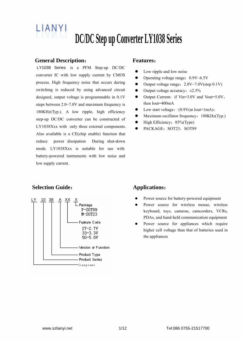
LY 10 38 A XX X
lianyiwei

LY1038F M5 SOT23-5
www.szlianyi.net 2/12 Tel:086 0755-21517700
LY1038Cxx
LY1038Bxx
LY1038Axx
LY1038Dxx
LY1038Cxx
LY1038Bxx
LY1038Axx
TYPE POSTFIX PACKAGE SWITCHINGTRANSISTOR
CE FUNCTION FEATURES
M3 SOT23-3 P SOT89-3
Build in Transistor No Lx
M3 SOT23-3 P SOT89-3
External Transistor No Ext
M5 SOT23-5 P SOT89-5
Build in Transistor Yes Lx CE
M5 SOT23-5 P SOT89-5
External Transistor Yes Ext CE
External Transistor Yes Ext
Pin Configuration:
Pin Assignment: PIN Number
SOT23-3 SOT89-3 PIN
NAME FUNCTION
1 1 Vss Ground 3 2 Vout Output voltage monitor, IC internal power supply 2 3 Lx Switch
PIN Number
SOT23-3 SOT89-3 PIN
NAME FUNCTION
1 1 Vss Ground 3 2 Vout Output voltage monitor, IC internal power supply 2 3 Ext External switch transistor drive
PIN Number
SOT23-5 SOT89-5 PIN
NAME FUNCTION
4 5 Vss Ground 2 2 Vout Output voltage monitor, IC internal power supply 5 4 Lx Switch 1 3 CE Chip enable 3 1 NC NC

www.szlianyi.net 3/12 Tel:086 0755-21517700
LY1038Fxx
LY1038Dxx
PIN Number
SOT23-5 SOT89-5 PIN NAME FUNCTION
4 5 Vss Ground 2 2 Vout Output voltage monitor, IC internal power supply 5 4 Ext External switch transistor drive 1 3 CE Chip enable 3 1 NC NC
PIN Number PIN NAME FUNCTION
SOT23-5 1 FB Feed Back 2 Vdd Output voltage monitor, IC internal power supply 3 NC NC 4 Vss Ground 5 EXT External switch transistor drive
Block Diagram:
Absolute Maximum Ratings: PARAMETER SYMBAL RATINGS UNITS
VIN Input Voltage VIN 6.5 V Lx Pin voltage VLX 6.5 V EXT Pin voltage VEXT -0.3~Vout+0.3 V
CE Pin voltage VCE -0.3~Vout+0.3 V Lx Pin current ILX 600 mA EXT Pin current IEXT ±30 mA
Vdd input voltage Vdd 6.5 V SOT23 Pd 300 mW Continuous Total
Power Dissipation SOT89 Pd 500 mW
Operating Ambient Temperature TOpr -25~+85 Storage Temperature Tstg -40~+125
Soldering temperature and time Tsolder 260, 10s

www.szlianyi.net 4/12 Tel:086 0755-21517700
LY1038Bxx/Dxx
LY1038Axx/Cxx
Electrical Characteristics: Measuring conditions:Unless otherwise specified , VIN=Vout*0.6,VSS=0V,IOUT=10mA,Topt=25。
Fosc=180kHz
SYMBOL PARAMETER CONDITIONS MIN TYP MAX UNITS
VOUT Output Voltage Vout*0.975 Vout Vout*1.025 V
Vstart Oscillation
Start-up Voltage IOUT=1mA, VIN:0→2V
0.8 0.9 V
Vhold Oscillation Hold
Voltage IOUT=1mA, VIN:2→0V 0.45 V
IDD1 Supply Current
1
No external component
Vout=Vout*0.95, 50 µA
IDD2 Supply Current
2 Vout=Vout+0.5V 9 µA
ILX Lx Switching Current
VLX=0.4V, Vout=Vout*0.95 360 mA
ILXleak Lx Leakage
Current Vout=VLX=6V 0.5 µA
Fosc Oscillation Frequency
Vout=set Vout*0.95 180 kHz
Maxdty Duty Ratio on(VLX“L”)side 84 %
EFFI Efficiency 85 %
Fosc=180kHz
SYMBOL PARAMETER CONDITIONS MIN TYP MAX UNITS
VOUT Output Voltage Vout*0.975 Vout Vout*1.025 V
Vstart Oscillation
Start-up Voltage IOUT=1mA, VIN:0→2V 0.8 0.9 V
Vhold Oscillation Hold
Voltage IOUT=1mA, VIN:2→0V
0.45 V
IDD1 Supply Current
1 No external component
Vout=Vout*0.95, 80 µA
IDD2 Supply Current
2 Vout=Vout+0.5V 12 µA
ILX Lx Switching Current
VLX=0.4V, Vout=Vout*0.95 360 mA
ILXleak Lx Leakage
Current Vout=VLX=6V 0.5 µA
Fosc Oscillation Frequency Vout=set Vout*0.95 180 kHz
Maxdty Duty Ratio on(VLX“L”)side 84 %
EFFI Efficiency 85 %

www.szlianyi.net 5/12 Tel:086 0755-21517700
LY1038 step-up DC/DC converter charges energy in
LY1038F
VFB=3.3V , Fosc=180kHz
SYMBOL PARAMETER CONDITIONS MIN TYP MAX UNITS
VFB Output
Feedback Voltage
3.22 3.3 3.38 V
Vstart Oscillation
Start-up Voltage IOUT=1mA, VIN:0→2V
0.8 0.9 V
Vhold Oscillation Hold
Voltage IOUT=1mA, VIN:2→0V
0.45 V
IDD1 Supply Current
1 No external component
Vout=Vout*0.95, 80 µA
IDD2 Supply Current
2 Vout=Vout+0.5V 10 µA
ILX Lx Switching Current
VLX=0.4V, Vout=Vout*0.95 360 mA
ILXleak Lx Leakage
Current Vout=VLX=6V 0.5 µA
Fosc Oscillation Frequency Vout=set Vout*0.95 180 kHz
Maxdty Duty Ratio on(VLX“L”)side 84 %
EFFI Efficiency 85 % Note:1、Diode use Schottky diode such as IN5817 or IN5819 (forward voltage drop:0.2V)
2、Inductor:33μH(r<0.5Ω) 3、Capacitor:Tantalum type 100μF
Operation: the inductor when Lx Transistor is on, and
discharges the energy with the addition of the energy from input power source thereto, so that a higher
output voltage than the input voltage is obtained. Following is the operation diagram.
Switching DC/DC Step up Converter operating process
www.szlianyi.net 6/12 Tel:086 0755-21517700
LY1038
Selection of Peripheral Components and Application Notes Peripheral components should be selected carefully because they are greatly affect the performances of
:
Use capacitor with a capacity of 10μF or more ( too small capacity will lead to high output ripple),
and with good frequency characteristics ( it is better to use Tantalum type). Besides, it is
recommended the use of a capacitor with an allowable voltage which is at least three times the
output set voltage. This is because there may be the case where a spike-shaped high voltage is
generated by the inductor when Lx transistor is turned OFF.
Choose such an inductor that has sufficiently small d.c. resistance and large allowable current, and
hardly reaches magnetic saturation. When the inductance value of the inductor is small, there may
be the case where ILX exceeds the absolute maximum ratings at the maximum load.
Use a diode of a Schottky type with high switching speed.
PCBLAYOUT:
Set external components as close as possible to the IC and minimize the connection between the
components and the IC. In particular, when an external component is connected to VOUT Pin, make
minimum connection with the capacitor.
Make Vss pin sufficient grounding, otherwise, the zero level within IC will varied with the
switching current. This may result in unstable operation of IC.

www.szlianyi.net 7/12 Tel:086 0755-21517700
Typical Applications:
Components: Inductor:47uH(Sumida ) Diode:IN5817、IN5819 Capacitor:47uF/16V(Tantalum type) Transistor:2SD1628G、2SD3279 NMOS:AAT9460、XP151、XP161 Base Resistor(Rb):1KΩ
Base Capacitor(Cb):2200pF RFB :Set up so that RFB1 /RFB2=Vout / VFB-1(Vout=set-up output voltage),
Please use with RFB1+RFB2≤2MΩ; CFB:Set up that Fzfb=1/(2×π×CFB×RFB1) is within the Adjustments necessary in respect of L,CL.

www.szlianyi.net 8/12 Tel:086 0755-21517700
Type Characteristics
LY1038
LY1038Xxxx

www.szlianyi.net 9/12 Tel:086 0755-21517700
L=47uH,Cout=47uF,Vout=100uF,SD:1N5717/5819
VDD=VOUT*0.95

www.szlianyi.net 10/12 Tel:086 0755-21517700
VDD=VOUT+0.5

www.szlianyi.net 11/12 Tel:086 0755-21517700
Package Dimensions:

www.szlianyi.net 12/12 Tel:086 0755-21517700