ddr interface design implementation white paper
TRANSCRIPT

1 DDR Interface Design Implementation
A Lattice Semiconductor White Paper
DDR Interface Design Implementation
A Lattice Semiconductor White Paper
December 2004
Lattice Semiconductor5555 Northeast Moore Ct.
Hillsboro, Oregon 97124 USATelephone: (503) 268-8000
www.latticesemi.com

2 DDR Interface Design Implementation
A Lattice Semiconductor White Paper
Memory Overview
Over the past several years the electronics market and, more specifically, the
memory market has undergone significant change. Prior to the electronics
industry downturn in 2000, electronic system designers were less concerned with
the cost of the components going into their next design, and more concerned
with the raw, maximum performance they could achieve.
Today, increasing competition and decreasing profit margins have forced system
designers to reduce next generation product cost while maintaining, or even
increasing, system performance. One industry segment that has experienced
substantial growth as a result of this transition is DRAM memory, particularly
Double Data Rate (DDR) SDRAM memory.
DDR Memory first came on the scene as a high performance, low-cost memory
solution targeted primarily at the personal computer and other cost sensitive
consumer markets. More recently, due to the economic pressures squeezing the
entire electronics industry, non-consumer products have also begun to
incorporate DDR memory (Figure 1).
DDR is an evolutionary memory technology based on SDRAM. DDR SDRAM
access is twice as fast as SDRAM, because DDR data transfers occur on both
edges of the clock, compared to SDRAM, which transfers data only on the rising
edge of a clock. Consequently, DDR can transfer data at up to 2133MB/s. DDR
also consumes much less power than conventional SDRAM, with an operational
Vcc of just 2.5Vdc instead of 3.3Vdc for SDRAM.

3 DDR Interface Design Implementation
A Lattice Semiconductor White Paper
Where DRAM Gets Used (4.3B Units)
PC
48%
Other
3%Servers
14%
Peripherals
4%
Consumer
10%
Graphics
9%
Comm
12%
Figure 1
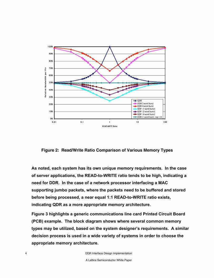
Market analyses indicate that DDR is currently utilized in over 50% of all
electronic systems, and usage is expected to increase to 80% over the next
several years. DDR is not, and will never be, an “all things to all designs”
technology. DDR memory is well suited for those designs that have a high
read to write ratio. Quad Data Rate memory, for example, is designed for
applications that require a 50% read/write ratio. Figure 2 identifies various
state of the art memory technologies and where on the read/write curve they
reside.
4 DDR Interface Design Implementation
A Lattice Semiconductor White Paper
Figure 2: Read/Write Ratio Comparison of Various Memory Types
As noted, each system has its own unique memory requirements. In the case
of server applications, the READ-to-WRITE ratio tends to be high, indicating a
need for DDR. In the case of a network processor interfacing a MAC
supporting jumbo packets, where the packets need to be buffered and stored
before being processed, a near equal 1:1 READ-to-WRITE ratio exists,
indicating QDR as a more appropriate memory architecture.
Figure 3 highlights a generic communications line card Printed Circuit Board
(PCB) example. The block diagram shows where several common memory
types may be utilized, based on the system designer’s requirements. A similar
decision process is used in a wide variety of systems in order to choose the
appropriate memory architecture.

5 DDR Interface Design Implementation
A Lattice Semiconductor White Paper
Figure 3: Utilization of Common Memory Types
The following list indicates the appropriate memory architecture for a variety of
systems and functions. These selections are based on the system architecture
and the respective performance/cost trade off requirements.
•Lookup - Fast Switching/Access time
–Latency Critical, Read Oriented, Smaller Bus Width (32/64bit)
–Memory Choice: ZBT (<10Gb/s) -> QDR/DDR (>10Gb/s)
–Operation: Address Translation
•Lookup - Large Size, High Throughput (Core Router)

6 DDR Interface Design Implementation
A Lattice Semiconductor White Paper
–Parity Required: Wide I/O (>64)
–Bandwidth and Granularity Required is Top Priority
–Memory Choice: SDR (<10Gb/s) -> DDR/FCRAM (10Gb/s) -> RLDRAM/DDR II (10Gb/s-40Gb/s)
–Operation: Address Translation
•Queue/Packet Management
–Latency #1, Random Read & Write - Unpredictable data pattern
–Memory Choice: ZBT -> QDR
–Operation: Queue management and flow control
•Traffic Shaping/Policing
–Burst Oriented, Narrow I/O Bus (x18/x36)
–Memory Choice: ZBT/QDR
–Operation: Policy based routing tables
•Statistics
–Random Read/Write, Read Dominant, Narrow I/O Bus (x18/x36)
–Memory Choice: ZBT/QDR
–Operation: Tracking data for packets, traffic statistics
•Packet Cell Buffer
–Large Granularity, Wide I/O Bus (>64bit)
–Bandwidth top priority
–Cost sensitive
–Memory choice: SDR -> DDR/FCRAM->RLDRAM/DDR II
–Operation: Handling IP Packets that vary in size (128B)
DDR Interface Design Implementation
Until now we have discussed various memory architectures and where they fit
within the system. Due to the relatively high acceptance rate of DDR in a growing
variety of digital designs, the remainder of this article will focus on DDR memory,
and implementation of the DDR interface within an FPGA.

7 DDR Interface Design Implementation
A Lattice Semiconductor White Paper
In many system designs, the engineer will elect to use an FPGA as the memory
controller (Figure 4). The advantage of using an FPGA is its inherent flexibility.
Regardless of the protocol or microprocessor, an FPGA fabric can generally
provide the DDR memory control and required electrical interface. A common
challenge in using an FPGA as a memory controller is the need for the high-
speed interface, such as that required by DDR. The required I/O speeds and
associated clocking are often challenging to implement, due to the non-
deterministic FPGA routing resources and limited I/O speeds of many FPGAs. At
DDR speeds over 200Mbps, environmental conditions such as temperature and
voltage will also affect the performance of the required I/O.DDR memory’s ability
to transfer data at double the standard SDRAM data rate is not an unmixed
blessing. The high speeds of DDR I/O, and the very short data windows of DDR
data, pose significant challenges. The speeds at which the memory controller
must reliably operate (200 MHz across FR-4 PCB traces) make the PCB layout
challenging. Furthermore, incorporating the DDR interface into a flexible FPGA
fabric presents the designer with the related complexity of meeting very critical
and tight timing in an inherently non-deterministic routing fabric. Designers
accustomed to the high-speed and flexibility of FPGAs are often surprised to find
that they have a difficult, if not impossible, experience getting a high-speed DDR
interface operating in an FPGA. These difficulties arise not from a functionality
issue, but from the physical realities of working with data windows that are well
within the magnitude of signal propagation delays in FR4 and FPGA routing.
These timing requirements are further complicated by the variation in logic speed
over process, temperature and voltage. Further complicating the implementation
of a DDR design is the need to handle and pre-process strobe signals, as
opposed to generic clock signals. The design engineer can no longer simply
connect data and address lines and expect to have a robust, high-speed memory
interface.

8 DDR Interface Design Implementation
A Lattice Semiconductor White Paper
Figure 4: FPGA As Memory Controller
Each FPGA vendor has approached the problem of DDR memory interfacing in its
own way. At one extreme, where limited resources are allocated in the I/O block,
the data de-muxing and/or clock transfer logic must be implemented in the FPGA
core logic, and the designer is likely to be forced to hand-route the interface logic
in order to guarantee the critical timing. At the other extreme, Lattice
Semiconductor’s recently introduced EC and ECP families provide a complete
hard-wire interface in the I/O block that addresses all of the functionality and
timing issues (including compensation for temperature and voltage) associated
with the interface, eliminating the problem of meeting timing in the FPGA core
routing resources. The latter approach guarantees success by design.

9 DDR Interface Design Implementation
A Lattice Semiconductor White Paper
Due to the complexity of a DDR memory design, it is worth considering some of
the aspects of the interface in more detail.
DDR SDRAM Interfaces Overview
In a typical non-DDR system, both the controller and memory in a system
transmit or capture data in response to a single system clock (Figure 5).
Designers became familiar with the timing constraints in these systems, which,
over time, have become tighter as clock speeds have increased.
The typical timing budget for the synchronous common clock system below
would include:
• Memory Access time (tAC)
• Data Propagation Delay (tPROP)
• Clock Skew from Controller to Memory (tSKEW)
• Temperature, Voltage Data-to-Clock (tTV)

10 DDR Interface Design Implementation
A Lattice Semiconductor White Paper
Figure 5: Typical Non-DDR System
As designers moved to a Double Data Rate implementation of these systems,
they achieved a 2X effective increase in the bit rate of the system. This
effectively cut the data window in half. Whereas the older common-clock
systems might have a data window of 6ns or more, designers are now faced
with DDR systems with windows of 2.5ns or less. The incremental speed
improvements, provided by smaller process geometries, that designers
depend on for performance gains are insufficient to make up for this halving
of the data window. To further complicate matters, these bit times are now
approaching the propagation time of signals on FR4 and in FPGA routing. Put
another way, a more substantial piece of the timing budget for a memory cycle
is being taken up by physical board routing delays and variations due to
temperature and voltage that do not improve as silicon geometries shrink.

11 DDR Interface Design Implementation
A Lattice Semiconductor White Paper
Figure 6: Tight Timing of a 2.5nS Window
Figure 6 illustrates the tight timing of a 2.5nS window, typical of a DDR
transfer. It is clear that the access and propagation times of today’s memories
make it impossible for DDR transfers to take place with a clock-controlled data
launch and capture system. For a DDR system to operate, the ability to launch
the data from the memory device at the same instant as a data-valid signal is
needed. This would effectively eliminate the memory access time and data
propagation time (both the strobe and data would experience the same
propagation time) from the timing budget, and significantly open the data-valid
window. The only remaining skews in this approach would be the small but
finite difference in the ability to launch both the data strobe and the data
simultaneously (tALIGN) (Figure 7).

12 DDR Interface Design Implementation
A Lattice Semiconductor White Paper
Figure 7: DDR Timing Margin: A Workable Solution
An Alternate Approach
To accomplish this method of data transfer, DDR SDRAM interfaces rely on the
use of a data strobe signal called DQS. DQS is generated from the differential
clock fed to the DDR memory and a DLL inside the DDR memory used to generate
and align DQS to outgoing data. Although a DDR memory does not use the
differential input clock to launch or capture data, the DQS signal that is used is
related to the incoming clock frequency. Figure 8 illustrates the new timing
parameters of a data window based on a DQS-based READ transfer. As noted
earlier, there is a finite skew between the launch of DQS and the last lane of data
(DQ) to become valid. This data-valid-to-data alignment error is called tDQSQ.
This delay reduces the size of the data valid window. In this system, there is also
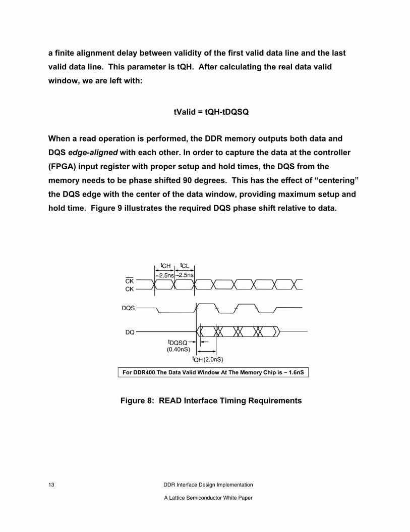
13 DDR Interface Design Implementation
A Lattice Semiconductor White Paper
a finite alignment delay between validity of the first valid data line and the last
valid data line. This parameter is tQH. After calculating the real data valid
window, we are left with:
tValid = tQH-tDQSQ
When a read operation is performed, the DDR memory outputs both data and
DQS edge-aligned with each other. In order to capture the data at the controller
(FPGA) input register with proper setup and hold times, the DQS from the
memory needs to be phase shifted 90 degrees. This has the effect of “centering”
the DQS edge with the center of the data window, providing maximum setup and
hold time. Figure 9 illustrates the required DQS phase shift relative to data.
Figure 8: READ Interface Timing Requirements

14 DDR Interface Design Implementation
A Lattice Semiconductor White Paper
Figure 9: Required DQS Phase Shift Relative to Data.
It is clear that there is now a reasonable data window from which to capturedata.
The DQS signal has several characteristics:
DQS is bi-directional
A DQS line is typically generated for 8 lanes of data from the DDRmemory
The phase of DQS relative to the data depends on the operation beingperformed (Write or Read)
DQS is not free running
In the memory device, DQS is generated by DLL to minimize the skewbetween it and data
DQS has a Preamble state just after the signal comes out of tristatewhere DQS goes low
DQS has a Postamble state just before returning to tristate where DQSgoes low
Figure 10 depicts a DDR memory and FPGA controller with the associated data
and control lanes. Again, note that DQS is bi-directional. Note that the clock
signal provided to the memory is differential (CLKP and CLKN) to minimize duty
cycle variations. It is important to understand that it is not the clock signal that is

15 DDR Interface Design Implementation
A Lattice Semiconductor White Paper
used to capture or launch data to or from the memory. DDR memory also
requires a Data Mask (DM) signal, which is used to mask data bits during the
write cycles. This allows writes to the memory on only one of the two edges of
DQS that occur in a cycle.
Figure 10: Typical DDR interface
Figure 11 illustrates the WRITE timing for a DDR interface. Here we are
looking at the signals as they exit from the FPGA controller. Note that the
FPGA controller launches DQS center-aligned with the data window. This
differs from the edge-aligned launch from the memory described earlier. Also
note the requirement that all data (for DDR400) must meet the setup and hold
times of 0.4ns relative to any DQS edge.

16 DDR Interface Design Implementation
A Lattice Semiconductor White Paper
Figure 11: DQ-DQS during WRITE
SDRAM interfaces typically are implemented with x8, x16 or x32 bits for each DQS
signal. Note that the ratio of DQS to data bits is independent of the overall width
of the memory.
Implementing DDR Memory Interfaces with FPGA Devices
Now that we have defined the requirements of a typical DDR interface, we can
turn to implementation of that DDR memory interface in an FPGA.
17 DDR Interface Design Implementation
A Lattice Semiconductor White Paper
Memory Read Implementation
Here we will examine the challenges encountered in the design of a READ
interface and the available solutions.
Challenges Encountered by the FPGA During Memory READ
1. DQS-DQ Alignment - DQS must be re-aligned (90 degree phase shift) tocapture read data within the narrow data valid window. The system level skewand skew across multiple DQ lines must be managed.
2. Data Mux and De-Mux - During READ, the DDR input data must be de-muxedinto two SDR streams.
3. Clock Domain Transfer - After the data is demuxed, the data must be alignedto a common clock edge and then must be synchronized to an unrelated FPGAsystem clock. The transfer to the FPGA clock domain must consider the relativephase of the DQS strobe and the FPGA system clock to avoid setup and holdviolations.
The Solution
FPGAs include features that simplify the implementation of the READ portion of aDDR interface. These may include:
• DLL compensated DQS delay elements
• DDR input registers
• Half-Clock transfer register
• Automatic DQS to system clock domain transfer circuitry
DDR Input Circuitry
A full implementation of a DDR receiver or input interface requires all of the
elements listed above. Figure 12 depicts the LatticeECP/EC FPGA
implementation that connects all of these elements together to implement the
read portion of a DDR memory interface.

18 DDR Interface Design Implementation
A Lattice Semiconductor White Paper
Figure 12: LatticeECP/EC DDR Input Circuitry
The DQS Delay Block receives the edge-aligned DQS signal from the memory and
performs the phase shift of 90 degrees. This phase shifted DQS signal can now
be used by the FPGA input registers to capture and de-mux the positive and
negative edge data. Note that following the register that captures the positive-
edge data is a negative edge triggered flop. This half-clock transfer register
transfers the positive edge data from the first register to the negative edge of
DQS so that both the positive and negative portions of the data are now
presented to the next register stage on the same negative edge of DQS. Finally,
the last register stage can now clock-in both halves of data on the same FPGA

19 DDR Interface Design Implementation
A Lattice Semiconductor White Paper
system clock edge. This edge, however, must be chosen carefully in order to
maximize the setup and hold time in transferring data from the DQS domain to the
FPGA system clock domain. This is the purpose of the clock edge select mux
shown above. The clock polarity selection method is detailed below.
The Devil is in the Details
It is important to note the very tight timing associated with the 5 registers in the
input section of a high-speed DDR recovery block. With data windows of 2.5 ns,
and even smaller setup and hold times, designers regularly run into routing and
logic delays that overwhelm the system timing requirements. Many FPGA
architectures require the designer to hand place and route these registers if the
design is to operate at speed. Even then, designers have difficulty achieving
DDR400 speeds over operating temperature and voltage.
Lattice Semiconductor now provides LatticeECP/EC FPGAs that incorporate all
five input registers and associated routing in a hard I/O block (IOB). This
guarantees performance and success by design. The designer simply connects
the I/O blocks and DQS sub-modules and is guaranteed a working interface.
On-Chip DLL Calibration
Due to the very tight timing, both skew and the actual delay of the DQS delay
block must be carefully controlled. A low-cost solution may use an open-loop
fixed delay block for DQS delay. The performance of this scheme, however, will
vary with temperature and voltage. This will limit the maximum attainable speed
of the DDR interface. In a more complete solution, the temperature, voltage and
process variations affecting the DQS delay block are compensated for in a
closed-loop fashion. Typically this can be done by dedicated DLL elements on
the FPGA that feed calibration data to each delay element. Figure 13 illustrates

20 DDR Interface Design Implementation
A Lattice Semiconductor White Paper
the DLL compensation method used in the LatticeECP/EC devices. In these
devices the aligned DQS is distributed to the input registers, with each DQS
supporting up to 8 DQ’s.
Figure 13: LatticeECP/EC DQS Alignment using on chip DLL
Automatic Clock Polarity Control
In a typical DDR memory interface design, the phase relation between the
incoming delayed DQS strobe and the internal system Clock (during the READ
cycle) is unknown. Many FPGA devices leave the resolution of this problem to
the user. The LatticeECP/EC families contain dedicated circuits to determine the
necessary system clock polarity, perform this selection and perform the transfer
of data between these domains. To prevent setup and hold violations at the

21 DDR Interface Design Implementation
A Lattice Semiconductor White Paper
domain transfer between DQS (delayed) and the system clock, a clock polarity
selector is used. This requires evaluation at the start of each READ cycle to
determine the proper FPGA system clock polarity (Figure 14). Prior to the READ
operation in DDR memories, DQS is in tristate (determined by termination).
Coming out of tristate, the DDR memory device drives DQS low in the Preamble
State. A dedicated circuit detects this transition and generates a signal indicating
the required polarity for the FPGA system clock (DDRCLKPOL). This signal is
used to control the polarity of the clock to the synchronizing registers.
Figure 14: LatticeECP/EC Automatic Clock Polarity Select
Memory Write Implementation
To implement the write portion of a DDR memory interface, two streams of single
data rate data must first be multiplexed together to form a stream with data
transitioning on both edges of the clock. Furthermore, the FPGA controller must

22 DDR Interface Design Implementation
A Lattice Semiconductor White Paper
launch the DQS signal center-aligned with outgoing data, DQ. The Data Mask
signal (DM) is also used during a write cycle.
It is the responsibility of the FPGA output control to edge-align the DDR output
signals (ADDRCMD, DQS, but not DQ and DM) to the rising edge of the outgoing
differential clock (CLKP/CLKN).
Challenges encountered by the FPGA during Memory WRITE:
1. DQS needs to be center aligned with the outgoing DDR Data and DQ.
2. The FPGA needs to generate Differential CLK signals (CLKP and CLKN).CLKP needs to be edge-aligned with the Address and Command signals.
3. The FPGA controller must meet the DDR interface specification for tDSSand tDSH parameters, defined as DQS falling to CLKP rising setup and holdtimes.
4. The DDR output data must be muxed from two SDR streams into a singleoutgoing DDR data stream.
The Solution
A full-featured FPGA solution includes a pair of DDR output registers, output mux
and tri-state registers, along with PLLs that allow easy implementation of the
various output clock phases necessary in the write portion of the DDR memory
interfaces.
DDR Output Logic
The DDR output register block allows 2 SDR data streams to be muxed to a single
DDR data stream. The DDR tristate registers simplify implementation for bi-
directional signals. Figure 15 illustrates these capabilities for the LatticeECP/EC
devices.

23 DDR Interface Design Implementation
A Lattice Semiconductor White Paper
Figure 15: LatticeECP/EC DDR Output Logic
The Write control circuit must create several phases of the system clock to
appropriately launch the respective control signals from the FPGA:
1. A PLL is used to generate a 90-degree phase shifted clock. This 90-degreephase shifted clock will be used to generate DQS, address, command andthe differential clocks going to the memory. Note that ADDRESS and CMDonly change at the clock rate (SDR). Address and data are then edge-aligned with DQS and the CLKP/N signals. This allows the tDSS and tDSHspecs to be met.
2. The DDR clock can be generated by assigning “0” and “1” to the inputs ofthe DDR output register pair. This is then fed into a SSTL25 differentialoutput buffer to generate CLKP and CLKN differential clocks. Generatingthe CLKN in this manner would prevent any skew between the 2 signals.
3. Since internally the DQS and ADDR/CMD signals are generated using theprimary FPGA clock, the user will need to implement a _ clock transfer

24 DDR Interface Design Implementation
A Lattice Semiconductor White Paper
from the core logic to the DDR registers. Timing can be hard to meet, so Itis recommended that the user first register these signals with the invertedClock, so that the transfer from the core logic to the I/O registers will onlyrequire a _ clock transfer.
4. The data DQ and DM need to be delayed by 90° as they leave the FPGA.This is to center the data and data mask relative to the DQS when itreaches the DDR memory. This can be accomplished by inverting the CLKto the DQ and DM data. The DM signal is generated using the same clockas the DQ data pin. The memory masks the DQ signals if the DM pins aredriven high.
Figure 16 illustrates DDR Write interface signal generation for the LatticeECP/EC
devices.
Figure 16: LatticeECP/EC Memory WRITE Interface Signal Generation

25 DDR Interface Design Implementation
A Lattice Semiconductor White Paper
SUMMARY
As discussed throughout this article, there are a wide variety of memory options
available to system designers. Careful consideration is essential when
evaluating a specific type of memory for a particular application. We also
conclude that DDR is increasingly becoming the memory of choice for a majority
of systems. The advantages of DDR are significant compared to other memory
options; however, DDR is a high-speed, complex interface that requires special
care for proper implementation. Fortunately, FPGA manufacturers have begun to
implement turnkey solutions that provide design flexibility yet guarantee
performance and a robust solution.
###