advantechadvdownload.advantech.com/productfile/pis/aqd-d3l2gn16...240pin ddr3l 1.35v 1600 u-dimm 2gb...
TRANSCRIPT

240Pin DDR3L 1.35V 1600 U-DIMM
2GB Based on 256Mx8
AQD-D3L2GN16-SQ1
1
Advantech
AQD-D3L2GN16-SQ1
Datasheet
Rev. 0.0
2017-07-07

240Pin DDR3L 1.35V 1600 U-DIMM
2GB Based on 256Mx8
AQD-D3L2GN16-SQ1
2
Description
AQD-D3L2GN16-SQ1 is a DDR3L 1600Mbps U-DIMM
high-speed, memory module that use 8pcs of 256Mx 64
bits DDR3L SDRAM in FBGA package and a 2K bits
serial EEPROM on a 240-pin printed circuit board.
AQD-D3L2GN16-SQ1 is a Dual In-Line Memory Module
and is intended for mounting into 240-pin edge connector
sockets.
Synchronous design allows precise cycle control with the
use of system clock. Data I/O transactions are possible
on both edges of DQS. Range of operation frequencies,
programmable latencies allow the same device to be
useful for a variety of high bandwidth, high performance
memory system applications.
Features
Lead-free and Halogen free products are RoHS
Compliant
JEDEC standard 1.35V(1.28V~1.45V) Power supply
Backward compatible for 1.5V(1.425V~1.575V)
VDDQ=1.35V(1.28V~1.45V) & 1.5V(1.425V~1.575V)
MRS Cycle with address key programs
- CAS Latency( 5,6,7,8,9,10,11)
- Burst Length (BL):8 and 4 with Burst Chop(BC)
Bi-directional, differential data strobe (DQS and /DQS)
Differential clock input (CK, /CK) operation
8 bit pre-fetch
Double-data-rate architecture; two data transfers per
clock cycle
Internal calibration through ZQ pin
On Die Termination with ODT pin
Auto refresh and self refresh
Average Refresh Period 7.8us at lower than TCASE
85°C, 3.9us at 85°C < TCASE ≤ 95°C
PCB Gold Plating: 30u” min
Pin Identification
Symbol Function
A0~A14, BA0~BA2 Address/Bank input
DQ0~DQ63 Bi-direction data bus.
DQS0~DQS7 Data strobes
/DQS0~/DQS7 Differential Data strobes
CK0, /CK0,CK1, /CK1 Clock Input. (Differential pair)
CKE0, CKE1 Clock Enable Input.
ODT0, ODT1 On-die termination control line
/S0, /S1 DIMM rank select lines.
/RAS Row address strobe
/CAS Column address strobe
/WE Write Enable
DM0~DM7 Data masks/high data strobes
VDD Core power supply
VDDQ I/O driver power supply
VREFDQ DQ reference supply
VREFCA Command/address reference
supply
VDDSPD SPD EEPROM power supply
SA0~SA2 I2C serial bus address select for
EEPROM
SCL I2C serial bus clock for EEPROM
SDA I2C serial bus data for EEPROM
VSS Ground
/RESET Set DRAMs Known State
VTT DRAM I/O termination supply
NC No Connection

240Pin DDR3L 1.35V 1600 U-DIMM
2GB Based on 256Mx8
AQD-D3L2GN16-SQ1
3
Dimensions (Unit: millimeter)
Note:1. Tolerances on all dimensions +/-0.15mm unless otherwise specified.

240Pin DDR3L 1.35V 1600 U-DIMM
2GB Based on 256Mx8
AQD-D3L2GN16-SQ1
4
Pin Assignments
Pin
No
Pin
Name
Pin
No
Pin
Name
Pin
No
Pin
Name
Pin
No
Pin
Name
Pin
No
Pin
Name
Pin
No
Pin
Name
1 VREFDQ 41 VSS 81 DQ32 121 VSS 161 NC,DM8 201 DQ37
2 VSS 42 NC 82 DQ33 122 DQ4 162 NC 202 VSS
3 DQ0 43 NC 83 VSS 123 DQ5 163 VSS 203 DM4
4 DQ1 44 VSS 84 /DQS4 124 VSS 164 NC,CB6 204 NC
5 VSS 45 NC,CB2 85 DQS4 125 DM0 165 NC,CB7 205 VSS
6 /DQS0 46 NC,CB3 86 VSS 126 NC 166 VSS 206 DQ38
7 DQS0 47 VSS 87 DQ34 127 VSS 167 NC 207 DQ39
8 VSS 48 NC 88 DQ35 128 DQ6 168 /RESET 208 VSS
9 DQ2 49 NC 89 VSS 129 DQ7 169 CKE1,NC 209 DQ44
10 DQ3 50 CKE0 90 DQ40 130 VSS 170 VDD 210 DQ45
11 VSS 51 VDD 91 DQ41 131 DQ12 171 A15 211 VSS
12 DQ8 52 BA2 92 VSS 132 DQ13 172 A14 212 DM5
13 DQ9 53 NC 93 /DQS5 133 VSS 173 VDD 213 NC
14 VSS 54 VDD 94 DQS5 134 DM1 174 A12 214 VSS
15 /DQS1 55 A11 95 VSS 135 NC 175 A9 215 DQ46
16 DQS1 56 A7 96 DQ42 136 VSS 176 VDD 216 DQ47
17 VSS 57 VDD 97 DQ43 137 DQ14 177 A8 217 VSS
18 DQ10 58 A5 98 VSS 138 DQ15 178 A6 218 DQ52
19 DQ11 59 A4 99 DQ48 139 VSS 179 VDD 219 DQ53
20 VSS 60 VDD 100 DQ49 140 DQ20 180 A3 220 VSS
21 DQ16 61 A2 101 VSS 141 DQ21 181 A1 221 DM6
22 DQ17 62 VDD 102 /DQS6 142 VSS 182 VDD 222 NC
23 VSS 63 CK1,NC 103 DQS6 143 DM2 183 VDD 223 VSS
24 /DQS2 64 /CK1,NC 104 VSS 144 NC 184 CK0 224 DQ54
25 DQS2 65 VDD 105 DQ50 145 VSS 185 /CK0 225 DQ55
26 VSS 66 VDD 106 DQ51 146 DQ22 186 VDD 226 VSS
27 DQ18 67 VREFCA 107 VSS 147 DQ23 187 NC,/EVENT 227 DQ60
28 DQ19 68 NC 108 DQ56 148 VSS 188 A0 228 DQ61
29 VSS 69 VDD 109 DQ57 149 DQ28 189 VDD 229 VSS
30 DQ24 70 A10/AP 110 VSS 150 DQ29 190 BA1 230 DM7
31 DQ25 71 BA0 111 /DQS7 151 VSS 191 VDD 231 NC
32 VSS 72 VDD 112 DQS7 152 DM3 192 /RAS 232 VSS
33 /DQS3 73 /WE 113 VSS 153 NC 193 /S0 233 DQ62
34 DQS3 74 /CAS 114 DQ58 154 VSS 194 VDD 234 DQ63
35 VSS 75 VDD 115 DQ59 155 DQ30 195 ODT0 235 VSS
36 DQ26 76 /S1,NC 116 VSS 156 DQ31 196 A13 236 VDDSPD
37 DQ27 77 ODT1,NC 117 SA0 157 VSS 197 VDD 237 SA1
38 VSS 78 VDD 118 SCL 158 NC,CB4 198 NC 238 SDA
39 NC,CB0 79 NC 119 SA2 159 NC,CB5 199 VSS 239 VSS
40 NC,CB1 80 VSS 120 VTT 160 VSS 200 DQ36 240 VTT
/S1,ODT1,CKE1:Used for dual-rank UDIMMs; NC on single-rank UDIMMs.
CK1 and /CK1:Used for dual-rank UDIMMs; not used on single-rank UDIMMs but terminated.
240Pin DDR3L 1.35V 1600 U-DIMM
2GB Based on 256Mx8
AQD-D3L2GN16-SQ1
5
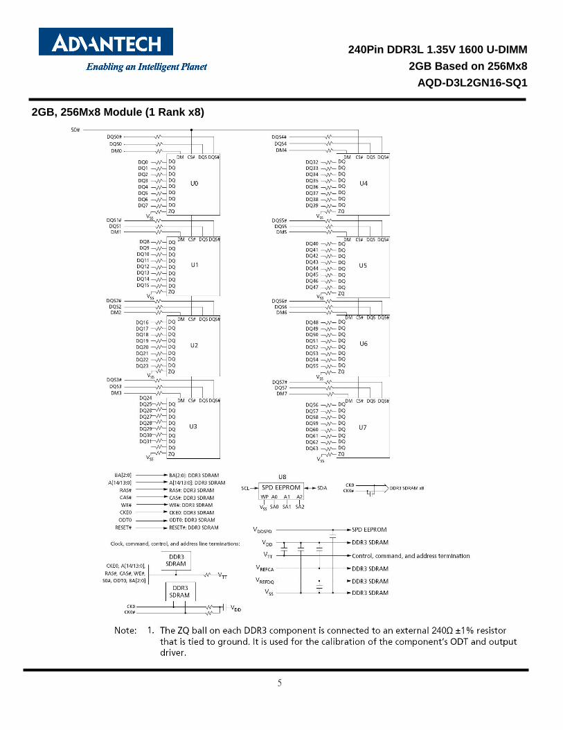
2GB, 256Mx8 Module (1 Rank x8)
240Pin DDR3L 1.35V 1600 U-DIMM
2GB Based on 256Mx8
AQD-D3L2GN16-SQ1
6
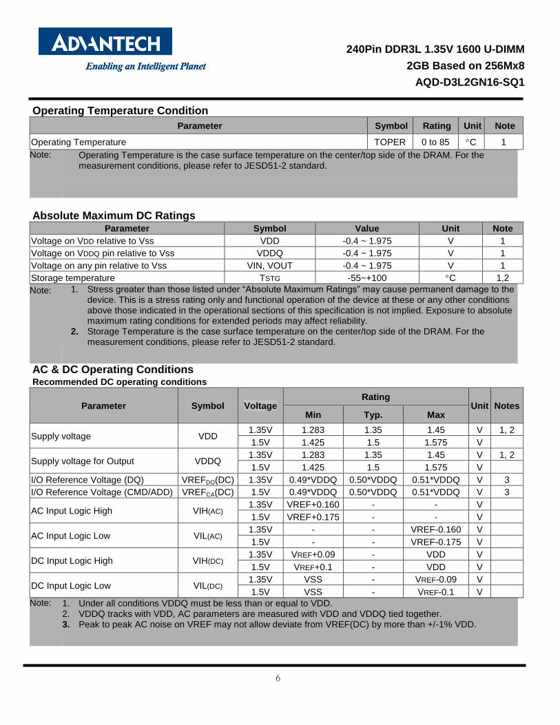
Operating Temperature Condition
Parameter Symbol Rating Unit Note
Operating Temperature TOPER 0 to 85 C 1
Note: Operating Temperature is the case surface temperature on the center/top side of the DRAM. For the measurement conditions, please refer to JESD51-2 standard.
Absolute Maximum DC Ratings
Parameter Symbol Value Unit Note
Voltage on VDD relative to Vss VDD -0.4 ~ 1.975 V 1
Voltage on VDDQ pin relative to Vss VDDQ -0.4 ~ 1.975 V 1
Voltage on any pin relative to Vss VIN, VOUT -0.4 ~ 1.975 V 1
Storage temperature TSTG -55~+100 C 1,2
Note: 1. Stress greater than those listed under “Absolute Maximum Ratings” may cause permanent damage to the device. This is a stress rating only and functional operation of the device at these or any other conditions above those indicated in the operational sections of this specification is not implied. Exposure to absolute maximum rating conditions for extended periods may affect reliability.
2. Storage Temperature is the case surface temperature on the center/top side of the DRAM. For the measurement conditions, please refer to JESD51-2 standard.
AC & DC Operating Conditions
Recommended DC operating conditions
Parameter Symbol Voltage Rating
Unit Notes Min Typ. Max
Supply voltage VDD 1.35V 1.283 1.35 1.45 V 1, 2
1.5V 1.425 1.5 1.575 V
Supply voltage for Output VDDQ 1.35V 1.283 1.35 1.45 V 1, 2
1.5V 1.425 1.5 1.575 V
I/O Reference Voltage (DQ) VREFDQ(DC) 1.35V 0.49*VDDQ 0.50*VDDQ 0.51*VDDQ V 3
I/O Reference Voltage (CMD/ADD) VREFCA(DC) 1.5V 0.49*VDDQ 0.50*VDDQ 0.51*VDDQ V 3
AC Input Logic High VIH(AC) 1.35V VREF+0.160 - - V
1.5V VREF+0.175 - - V
AC Input Logic Low VIL(AC) 1.35V - - VREF-0.160 V
1.5V - - VREF-0.175 V
DC Input Logic High VIH(DC) 1.35V VREF+0.09 - VDD V
1.5V VREF+0.1 - VDD V
DC Input Logic Low VIL(DC) 1.35V VSS - VREF-0.09 V
1.5V VSS - VREF-0.1 V
Note: 1. Under all conditions VDDQ must be less than or equal to VDD. 2. VDDQ tracks with VDD, AC parameters are measured with VDD and VDDQ tied together. 3. Peak to peak AC noise on VREF may not allow deviate from VREF(DC) by more than +/-1% VDD.

240Pin DDR3L 1.35V 1600 U-DIMM
2GB Based on 256Mx8
AQD-D3L2GN16-SQ1
7
IDD Specification parameters Definition - 2GB (1 Rank x8)
Parameter Symbol DDR3L 1600 CL11 Unit
Operating One bank Active-Precharge current; tCK = tCK(IDD), tRC =
tRC(IDD), tRAS = tRASmin(IDD); CKE is HIGH, /CS is HIGH between valid commands;Address bus inputs are SWITCHING; Data bus inputs are SWITCHING
IDD0 496 mA
Operating One bank Active-read-Precharge current; IOUT = 0mA; BL =
8, CL = CL(IDD), AL = 0; tCK = tCK(IDD), tRC = tRC (IDD), tRAS = tRASmin(IDD), tRCD = tRCD(IDD); CKE is HIGH, /CS is HIGH between valid commands; Address bus inputs are SWITCHING; Data pattern is same as IDD4W
IDD1 568 mA
Precharge power-down current; All banks idle; tCK = tCK(IDD); CKE is
LOW; Other control and address bus inputs are STABLE; Data bus inputs are FLOATING
IDD2P 88 mA
Precharge quiet standby current; All banks idle; tCK = tCK(IDD); CKE is
HIGH, /CS is HIGH; Other control and address bus inputs are STABLE; Data bus inputs are FLOATING
IDD2Q 256 mA
Precharge standby current; All banks idle; tCK = tCK(IDD); CKE is HIGH,
/CS is HIGH; Other control and address bus inputs are SWITCHING; Data bus inputs are SWITCHING
IDD2N 256 mA
Active power - down current; All banks open; tCK = tCK(IDD); CKE is LOW;
Other control and address bus inputs are STABLE; Data bus inputs are FLOATING IDD3P 256 mA
Active standby current; All banks open; tCK = tCK(IDD), tRAS =
tRASmax(IDD), tRP = tRP(IDD); CKE is HIGH, /CS is HIGH between valid commands; Other control and address bus inputs are SWITCHING; Data bus inputs are SWITCHING
IDD3N 336 mA
Operating burst read current; All banks open, Continuous burst reads, IOUT
= 0mA; BL = 4, CL = CL(IDD), AL = 0; tCK = tCK(IDD), tRAS = tRASmax(IDD), tRP = tRP(IDD); CKE is HIGH, /CS is HIGH between valid commands; Address bus inputs are SWITCHING; Data pattern is same as IDD4W
IDD4R 1280 mA
Operating burst write current; All banks open, Continuous burst writes; BL =
8, CL = CL(IDD), AL = 0; tCK = tCK(IDD), tRAS = tRASmax(IDD), tRP = tRP(IDD); CKE is HIGH, /CS is HIGH between valid commands; Address bus inputs are SWITCHING; Data bus inputs are SWITCHING IDD4R
IDD4W 1160 mA
Burst refresh current; tCK = tCK(IDD); Refresh command at every tRFC(IDD)
interval; CKE is HIGH, /CS is HIGH between valid commands; Other control and address bus inputs are SWITCHING; Data bus inputs are SWITCHING
IDD5 1080 mA
Self refresh current; CK and /CK at 0V; CKE ≒ 0.2V; Other control and
address bus inputs are FLOATING; Data bus inputs are FLOATING IDD6 88 mA
Operating bank interleave read current; All bank interleaving reads, IOUT =
0mA; BL = 8, CL = CL(IDD), AL = tRCD(IDD)-1*tCK(IDD); tCK = tCK(IDD), Trc = tRC(IDD), tRRD = tRRD(IDD), tRCD = 1*tCK(IDD); CKE is HIGH, CS is HIGH between valid commands;Address bus inputs are STABLE during DESELECTs; Data pattern is same as IDD4R;
IDD7 1680 mA
Note: 1.Module IDD was calculated on the specific brand DRAM(4xnm) component IDD and can be differently
measured according to DQ loading capacitor.

240Pin DDR3L 1.35V 1600 U-DIMM
2GB Based on 256Mx8
AQD-D3L2GN16-SQ1
8
Timing Parameters & Specifications
Speed DDR3L 1600 Unit
Parameter Symbol Min Max
Average Clock Period tCK 8 - ns
CK high-level width tCH 0.47 0.53 tCK
CK low-level width tCL 0.47 0.53 tCK
DQS, /DQS to DQ skew, per group, per access
tDQSQ - 125 ps
DQ output hold time from DQS, /DQS tQH 0.38 - tCK
DQ low-impedance time from CK, /CK tLZ(DQ) -450 225 ps
DQ high-impedance time from CK, /CK
tHZ(DQ) - 225 ps
Data setup time to DQS, /DQS reference to Vih(ac)Vil(ac) levels
tDS 10 - ps
Data hold time to DQS, /DQS reference to Vih(ac)Vil(ac) levels
tDH 45 ps
DQ and DM input pulse width for each input
tDIPW 360 - ps
DQS, /DQS Read preamble tRPRE 0.9 - tCK
DQS, /DQS differential Read postamble
tRPST 0.3 - tCK
DQS, /DQS Write preamble tWPRE 0.9 - tCK
DQS, /DQS Write postamble tWPST 0.3 - tCK
DQS, /DQS low-impedance time tLZ(DQS) -450 225 ps
DQS, /DQS high-impedance time tHZ(DQS) - 225 ps
DQS, /DQS differential input low pulse width
tDQSL 0.45 0.55 tCK
DQS, /DQS differential input high pulse width
tDQSH 0.45 0.55 tCK
DQS, /DQS rising edge to CK, /CK rising edge
tDQSS -0.27 0.27 tCK
DQS, /DQS falling edge setup time to CK, /CK rising edge
tDSS 0.18 - tCK
DQS, /DQS falling edge hold time to CK, /CK rising edge
tDSH 0.18 - tCK
Delay from start of Internal write transaction to Internal read command
tWTR Max
(4tck, 7.5ns) -
Write recovery time tWR 15 - ns
Mode register set command cycle time
tMRD 4 - tCK
/CAS to /CAS command delay tCCD 4 - nCK
Auto precharge write recovery + precharge time
tDAL tWR+tRP/tck nCK
240Pin DDR3L 1.35V 1600 U-DIMM
2GB Based on 256Mx8
AQD-D3L2GN16-SQ1
9
Active to active command period for 1KB page size
tRRD Max
(4tck, 7.5ns) - ns
Speed DDR3L 1600 Unit
Parameter Symbol Min Max
Active to active command period for 2KB page size
tRRD Max
(4tck, 6ns) -
Four Activate Window for 1KB page size
tFAW 30 - ns
Power-up and RESET calibration time tZQinitl 512 - tCK
Normal operation Full calibration time tZQoper 256 - tCK
Normal operation short calibration time
tZQcs 64 - tCK
Exit self refresh to commands not requiring a locked DLL
tXS Max
(5tCK, tRFC+10ns) -
Exit self refresh to commands requiring a locked DLL
tXSDLL tDLL(min) - tCK
Internal read to precharge command delay
tRTP Max
(4tck, 7.5ns) -
Minimum CKE low width for Self refresh entry to exit timing
tCKESR tCK(min)+1tCK -
Exit power down with DLL to any valid command: Exit Precharge Power Down with DLL
tXP Max
(3tCK, 6ns) -
CKE minimum pulse width (high and low pulse width)
tCKE Max
(3tCK, 5ns)
Asynchronous RTT turn-on delay (Power-Down mode)
tAONPD 2 8.5 ns
Asynchronous RTT turn-off delay (Power-Down mode)
tAOFPD 2 8.5 ns
ODT turn-on tAON -225 225 ps
ODT turn-off tAOF 0.3 0.7 tCK

240Pin DDR3L 1.35V 1600 U-DIMM
2GB Based on 256Mx8
AQD-D3L2GN16-SQ1
10
SERIAL PRESENCE DETECT SPECIFICATION (AQD-D3L2GN16-SQ1 Serial Presence Detect)

240Pin DDR3L 1.35V 1600 U-DIMM
2GB Based on 256Mx8
AQD-D3L2GN16-SQ1
11
Note: 1. Byte 119 -- Manufacturing location by manufacturing location (00:Taiwan /01:China)
2. Byte 120 -- Module manufacturing date by year (YY).
3. Byte 121 -- Module manufacturing date by week (WW).
4. Bytes 122~125 -- Module Serial Number.
5. Bytes 128~145 -- Manufacturer Part Number by module part number , (Unused digits are coded as ASCII blanks (20h)).
6. Bytes 152~163 -- Manufacturer's Specific Data by working order number. (Unused digits are coded as 00h.)
7. Bytes 164~175 -- Manufacturer's Specific Data by SPD naming number. (Unused digits are coded as 00h.)
8. Bytes 176~255 --These bytes are undefined and can be used for ADATA's own purpose. (Unused digits are coded as 00h.)