ddr4 (pc4) ecc udimm vr9muxx72x8xxx sheets/viking pdfs... · ddr4 288-pin udimm pin wiring ... nc...
TRANSCRIPT

Datasheet 3/19/2017
PS9MUxx72x8xxx Viking Technology
Revision A Page 1 of 42
vikingtechnology.com
DDR4 (PC4) ECC UDIMM
VR9MUxx72x8xxx
The Viking DDR4 UDIMM memory module offers lower operating voltages, higher module densities and faster speed categories than the prior DDR3 generation. JEDEC DDR4 (JESD79-4) has been defined to provide higher performance, with improved reliability and reduced power, thereby representing a significant achievement relative to previous DRAM memory technologies.

Datasheet 3/19/2017
PS9MUxx72x8xxx Viking Technology
Revision A Page 2 of 42
vikingtechnology.com
REVISION HISTORY
Revision Release Date Description of Change Checked By (Full Name)
A
3/19/17 Initial release 2/2/15 Revise CAS Latency Addressing table for 4Gb Key timing parameters for 2400Mt/s speed. IDD/IPP values. Updated 8Gb Device IDD values. Change in page size. correct Min & Max values that were swapped. changes in values @ CWL -9. change in value for 2400 timing parameters. Revise block diagram 5/13/15 Updated company logo, address and document format 2/12/17 Add 2666 timing. Change to CL17 for 2400 speed. Add 2666 PN’s

Datasheet 3/19/2017
PS9MUxx72x8xxx Viking Technology
Revision A Page 3 of 42
vikingtechnology.com
Legal Information
Legal Information Copyright© 2017 Sanmina Corporation. All rights reserved. The information in this document is proprietary and confidential to Sanmina Corporation. No part of this document may be reproduced in any form or by any means or used to make any derivative work (such as translation, transformation, or adaptation) without written permission from Sanmina. Sanmina reserves the right to revise this documentation and to make changes in content from time to time without obligation on the part of Sanmina to provide notification of such revision or change. Sanmina provides this documentation without warranty, term or condition of any kind, either expressed or implied, including, but not limited to, expressed and implied warranties of merchantability, fitness for a particular purpose, and non-infringement. While the information contained herein is believed to be accurate, such information is preliminary, and should not be relied upon for accuracy or completeness, and no representations or warranties of accuracy or completeness are made. In no event will Sanmina be liable for damages arising directly or indirectly from any use of or reliance upon the information contained in this document. Sanmina may make improvements or changes in the product(s) and/or the program(s) described in this documentation at any time. Sanmina, Viking Technology, Viking Modular Solutions, and the Viking logo are trademarks of Sanmina Corporation. Other company, product or service names mentioned herein may be trademarks or service marks of their respective owners.
STATEMENT OF COMPLIANCE Viking Technology, Sanmina Corporation ("Viking") shall use commercially reasonable efforts to provide components, parts, materials, products and processes to Customer that do not contain: (i) lead, mercury, hexavalent chromium, polybrominated biphenyls (PBB) and polybrominated diphenyl ethers (PBDE) above 0.1% by weight in homogeneous material or (ii) cadmium above 0.01% by weight of homogeneous material, except as provided in any exemption(s) from RoHS requirements (including the most current version of the "Annex" to Directive 2002/95/EC of 27 January, 2003), as codified in the specific laws of the EU member countries. Viking strives to obtain appropriate contractual protections from its suppliers in connection with the RoHS Directives. All printed circuit boards (PCBs) have a flammability rating of UL94V-0.

Datasheet 3/19/2017
PS9MUxx72x8xxx Viking Technology
Revision A Page 4 of 42
vikingtechnology.com
288 pin Ordering Information and Module Configuration
Viking Part Number Voltage Capacity Module
Configuration Device
Configuration Device
Package
DIMM Ranks Speed CAS Latency
VR9MU127228HBHyz 1.2V 4GB 512Mx72 512Mx8 (9) 4Gb FBGA 1 PC4-17000 CL15 (15-15-15)
VR9MU127228HBJyz1 1.2V 4GB 512Mx72 512Mx8 (9) 4Gb FBGA 1 PC4-19200 CL17 (17-17-17)
VR9MU127228HBKyz1 1.2V 4GB 512Mx72 512Mx8 (9) 4Gb FBGA 1 PC4-21300 CL19 (19-19-19)
VR9MU1G7228HBHyz 1.2V 8GB 1Gx72 512Mx8 (18) 4Gb FBGA 2 PC4-17000 CL15 (15-15-15)
VR9MU1G7228HBJyz1 1.2V 8GB 1Gx72 512Mx8 (18) 4Gb FBGA 2 PC4-19200 CL17 (17-17-17)
VR9MU1G7228HBKyz1 1.2V 8GB 1Gx72 512Mx8 (18) 4Gb FBGA 2 PC4-21300 CL19 (19-19-19)
VR9MU1G7228JBHyz 1.2V 8GB 1Gx72 1024Mx8 (9) 8Gb FBGA 1 PC4-17000 CL15 (15-15-15)
VR9MU1G7228JBJyz1 1.2V 8GB 1Gx72 1024Mx8 (9) 8Gb FBGA 1 PC4-19200 CL17 (17-17-17)
VR9MU1G7228JBKyz1 1.2V 8GB 1Gx72 1024Mx8 (9) 8Gb FBGA 1 PC4-21300 CL19 (19-19-19)
VR9MU2G7228JBHyz 1.2V 16GB 2Gx72 1024Mx8 (18) 8Gb FBGA 2 PC4-17000 CL15 (15-15-15)
VR9MU2G7228JBJyz1 1.2V 16GB 2Gx72 1024Mx8 (18) 8Gb FBGA 2 PC4-19200 CL17 (17-17-17)
VR9MU2G7228JBKyz1 1.2V 16GB 2Gx72 1024Mx8 (18) 8Gb FBGA 2 PC4-21300 CL19 (19-19-19)
Notes: 1. Contact Viking for availability date 2. The lowercase letters y and z are wildcard characters that indicate DRAM vendor and die revisions and /or for customer specific locked
BOMs. Refer to the Viking part number coversheet for details.

Datasheet 3/19/2017
PS9MUxx72x8xxx Viking Technology
Revision A Page 5 of 42
vikingtechnology.com
Features JEDEC Standard Power Supply
o PC4: VDD = VDDQ = 1.2V± 5% (1.14V-1.26V) o External VPP = 2.5 Volt +10%, -5% o VDDSPD = 2.5V± 10% (2.25-2.75V)
288 pin Dual-In-Line Memory Module
Edge finger connector ramp zone to reduce insertion force
Point-to-Point topology to reduce loading
Pseudo-open drain (POD12) DQ lines
Internally generated VrefDQ
ECC recovery from command and parity errors
On-chip CA Parity detection for the command/address bus
Programmable CAS Latency: 13,15,17
Programmable CAS Write Latency (CWL).
Programmable Additive Latency (Posted CAS)
Per DRAM addressability is supported
Data Bus Inversion support for x8 devices
Selectable Fixed burst chop (BC4) of 4 and burst length (BL8) of 8 on-the-fly (OTF) via the mode register set (MRS)
8n prefetch with 2 or 4 selectable bank groups: 16 banks (4 bank groups x 4 banks per bank group)
Separate activation, read, write, refresh operations for each bank group
7 mode registers
Dynamic On-Die-Termination (ODT) and ODT Park for improved signal integrity.
Self Refresh and several Power Down Modes
DLL-off mode for power savings
System Level Timing Calibration Support via Write Leveling and Multi Purpose Register (MPR) Read Pattern
Serial Presence Detect with EEPROM
Two On-DIMM Thermal Sensors
Asynchronous Reset
Bidirectional Differentially Buffered Data Strobes(DQS)
UDIMM dimensions per JEDEC MO-309 maximum limits
RoHS Compliant
DDR4 SPEED BIN Nomenclature
Module Standard SDRAM Standard Clock
DDR4-14900 DDR4-1866 933 MHz
DDR4-17000 DDR4-2133 1066 MHz
DDR4-192001 DDR4-2400 1200 MHz
DDR4-213001 DDR4-2667 1333 MHz
DDR4-256001 DDR4-3200 1600 MHz
Notes: 1. Contact Viking for availability date
DDR4 Timing Summary
MT/s tCK (ns)
CAS Latency
(tCK) tRCD (ns) tRP (ns) tRAS (ns) tRC (ns)
CL-tRCD-tRP
DDR4-1866 1.071 13 13.92 13.92 34 47.92 13-13-13
DDR4-2133 0.93 15 14.06 14.06 33 47.05 15-15-15
DDR4-2400 0.83 17 14.16 14.16 32 46.16 17-17-17
DDR4-2666 0.75 22 14.25 14.25 32 46.25 19-19-19
Notes:
CL = CAS Latency, tRCD = Activate –to-Command Time, tRP = Precharge Time. Refer to Speed Bin tables for details.

Datasheet 3/19/2017
PS9MUxx72x8xxx Viking Technology
Revision A Page 6 of 42
vikingtechnology.com
Addressing
4GB(1Rx8)
512Mx8 DRAM 8GB(1Rx8)
1024Mx8 DRAM 16GB(2Rx8)
1024Mx8 DRAM
Bank Address
# of Bank Groups 4 4 4
BG Address BG0~BG1 BG0~BG1 BG0~BG1
Bank Address in a BG
BA0~BA1 BA0~BA1 BA0~BA1
Row Address A0~A14 64K:A0~A15 64K:A0~A15
Column Address A0~ A9 A0~ A9 A0~ A9
Page size 512B 512B 512B
Refresh Count 4K 8K 8K
Note:
Micron datasheet specified 512B / 1KB as page size with “Die revision dependant”.
In Hynix and Samsung Datasheet specfies 512B for x4 Device.

Datasheet 3/19/2017
PS9MUxx72x8xxx Viking Technology
Revision A Page 7 of 42
vikingtechnology.com
DDR4 288-pin UDIMM Pin Wiring Assignments/Configurations
Pin# Description Pin# Description Pin# Description Pin# Description Pin# Description Pin# Description
1 12V3, NC 145 12V
3, NC 52
DQS17_c, TDQS17_c 196 DQS8_c 102 DQ38 246 VSS
2 VSS 146 VREFCA 53 VSS 197 DQS8_t 103 VSS 247 DQ39
3 DQ4 147 VSS 54 CB6, NC 198 VSS 104 DQ34 248 VSS
4 VSS 148 DQ5 55 VSS 199 CB7, NC 105 VSS 249 DQ35
5 DQ0 149 VSS 56 CB2, NC 200 VSS 106 DQ44 250 VSS
6 VSS 150 DQ1 57 VSS 201 CB3, NC 107 VSS 251 DQ45
7
DQS9_t, DM0_n, DBI0_n, TDQS9_t 151 VSS 58 RESET_n 202 VSS 108 DQ40 252 VSS
8 DQS9_c, TDQS9_c 152 DQS0_c 59 VDD 203 CKE1 109 VSS 253 DQ41
9 VSS 153 DQS0_t 60 CKE0 204 VDD 110
DQS14_t, DM5_n, DBI5_n, TDQS14_t 254 VSS
10 DQ6 154 VSS 61 VDD 205 RFU 111 DQS14_c, TDQS14_c 255 DQS5_c
11 VSS 155 DQ7 62 ACT_n 206 VDD 112 VSS 256 DQS5_t
12 DQ2 156 VSS 63 BG0 207 BG1 113 DQ46 257 VSS
13 VSS 157 DQ3 64 VDD 208 ALERT_n 114 VSS 258 DQ47
14 DQ12 158 VSS 65 A12 209 VDD 115 DQ42 259 VSS
15 VSS 159 DQ13 66 A9 210 A11 116 VSS 260 DQ43
16 DQ8 160 VSS 67 VDD 211 A7 117 DQ52 261 VSS
17 VSS 161 DQ9 68 A8 212 VDD 118 VSS 262 DQ53
18
DQS10_t, DM1_n, DBI1_n, TDQS10_t 162 VSS 69 A6 213 A5 119 DQ48 263 VSS
19 DQS10_c, TDQS10_c 163 DQS1_c 70 VDD 214 A4 120 VSS 264 DQ49
20 VSS 164 DQS1_t 71 A3 215 VDD 121
DQS15_t, DM6_n, DBI6_n, TDQS15_t 265 VSS
21 DQ14 165 VSS 72 A1 216 A2 122 DQS15_c, TDQS15_c 266 DQS6_c
22 VSS 166 DQ15 73 VDD 217 VDD 123 VSS 267 DQS6_t
23 DQ10 167 VSS 74 CK0_t 218 CK1_t 124 DQ54 268 VSS
24 VSS 168 DQ11 75 CK0_c 219 CK1_c 125 VSS 269 DQ55
25 DQ20 169 VSS 76 VDD 220 VDD 126 DQ50 270 VSS
26 VSS 170 DQ21 77 VTT 221 VTT 127 VSS 271 DQ51
27 DQ16 171 VSS 78 EVENT_n 222 PARITY 128 DQ60 272 VSS
28 VSS 172 DQ17 79 A0 223 VDD 129 VSS 273 DQ61
29
DQS11_t, DM2_n, DBI2_n, TDQS11_t 173 VSS 80 VDD 224 BA1 130 DQ56 274 VSS
30 DQS11_c, 174 DQS2_c 81 BA0 225 A10_AP 131 VSS 275 DQ57
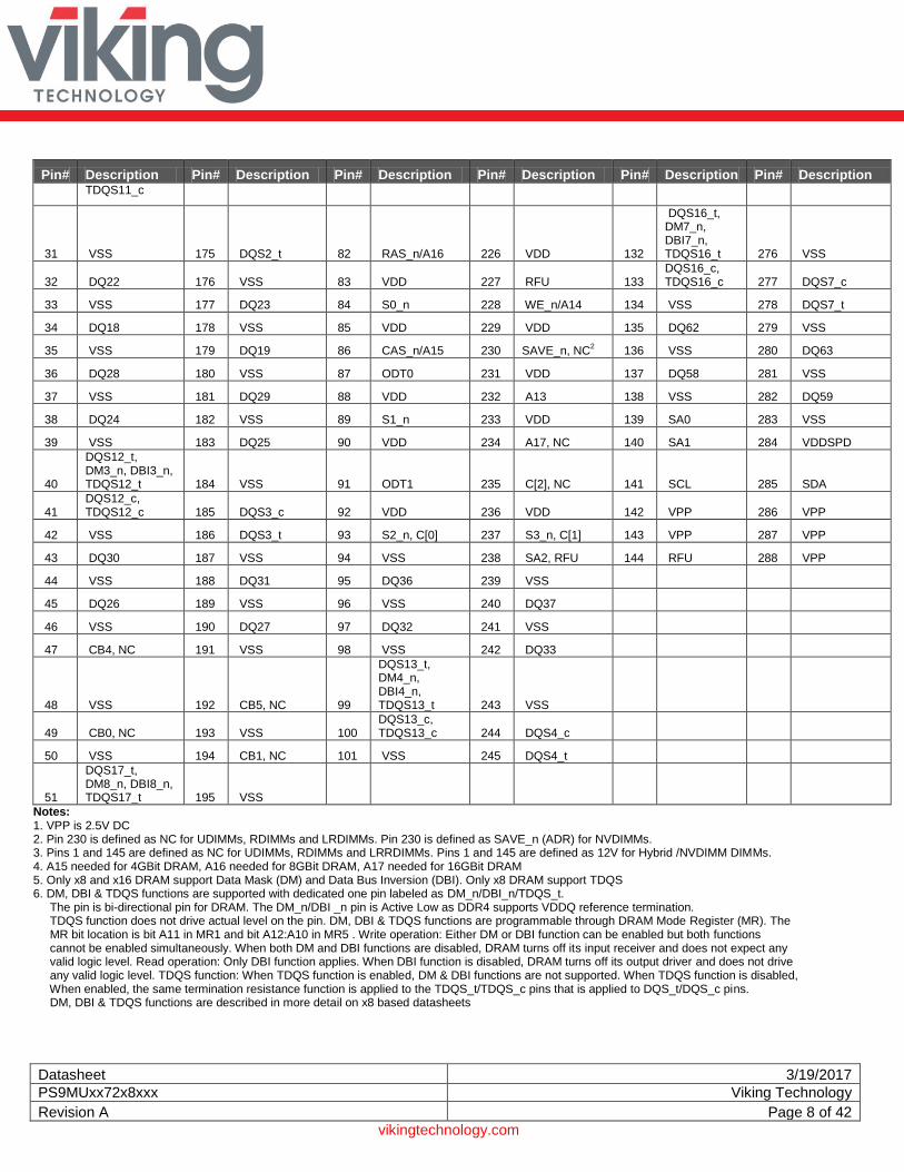
Datasheet 3/19/2017
PS9MUxx72x8xxx Viking Technology
Revision A Page 8 of 42
vikingtechnology.com
Pin# Description Pin# Description Pin# Description Pin# Description Pin# Description Pin# Description TDQS11_c
31 VSS 175 DQS2_t 82 RAS_n/A16 226 VDD 132
DQS16_t, DM7_n, DBI7_n, TDQS16_t 276 VSS
32 DQ22 176 VSS 83 VDD 227 RFU 133 DQS16_c, TDQS16_c 277 DQS7_c
33 VSS 177 DQ23 84 S0_n 228 WE_n/A14 134 VSS 278 DQS7_t
34 DQ18 178 VSS 85 VDD 229 VDD 135 DQ62 279 VSS
35 VSS 179 DQ19 86 CAS_n/A15 230 SAVE_n, NC2 136 VSS 280 DQ63
36 DQ28 180 VSS 87 ODT0 231 VDD 137 DQ58 281 VSS
37 VSS 181 DQ29 88 VDD 232 A13 138 VSS 282 DQ59
38 DQ24 182 VSS 89 S1_n 233 VDD 139 SA0 283 VSS
39 VSS 183 DQ25 90 VDD 234 A17, NC 140 SA1 284 VDDSPD
40
DQS12_t, DM3_n, DBI3_n, TDQS12_t 184 VSS 91 ODT1 235 C[2], NC 141 SCL 285 SDA
41 DQS12_c, TDQS12_c 185 DQS3_c 92 VDD 236 VDD 142 VPP 286 VPP
42 VSS 186 DQS3_t 93 S2_n, C[0] 237 S3_n, C[1] 143 VPP 287 VPP
43 DQ30 187 VSS 94 VSS 238 SA2, RFU 144 RFU 288 VPP
44 VSS 188 DQ31 95 DQ36 239 VSS
45 DQ26 189 VSS 96 VSS 240 DQ37
46 VSS 190 DQ27 97 DQ32 241 VSS
47 CB4, NC 191 VSS 98 VSS 242 DQ33
48 VSS 192 CB5, NC 99
DQS13_t, DM4_n, DBI4_n, TDQS13_t 243 VSS
49 CB0, NC 193 VSS 100 DQS13_c, TDQS13_c 244 DQS4_c
50 VSS 194 CB1, NC 101 VSS 245 DQS4_t
51
DQS17_t, DM8_n, DBI8_n, TDQS17_t 195 VSS
Notes: 1. VPP is 2.5V DC 2. Pin 230 is defined as NC for UDIMMs, RDIMMs and LRDIMMs. Pin 230 is defined as SAVE_n (ADR) for NVDIMMs. 3. Pins 1 and 145 are defined as NC for UDIMMs, RDIMMs and LRRDIMMs. Pins 1 and 145 are defined as 12V for Hybrid /NVDIMM DIMMs. 4. A15 needed for 4GBit DRAM, A16 needed for 8GBit DRAM, A17 needed for 16GBit DRAM 5. Only x8 and x16 DRAM support Data Mask (DM) and Data Bus Inversion (DBI). Only x8 DRAM support TDQS 6. DM, DBI & TDQS functions are supported with dedicated one pin labeled as DM_n/DBI_n/TDQS_t.
The pin is bi-directional pin for DRAM. The DM_n/DBI _n pin is Active Low as DDR4 supports VDDQ reference termination. TDQS function does not drive actual level on the pin. DM, DBI & TDQS functions are programmable through DRAM Mode Register (MR). The MR bit location is bit A11 in MR1 and bit A12:A10 in MR5 . Write operation: Either DM or DBI function can be enabled but both functions cannot be enabled simultaneously. When both DM and DBI functions are disabled, DRAM turns off its input receiver and does not expect any valid logic level. Read operation: Only DBI function applies. When DBI function is disabled, DRAM turns off its output driver and does not drive any valid logic level. TDQS function: When TDQS function is enabled, DM & DBI functions are not supported. When TDQS function is disabled, When enabled, the same termination resistance function is applied to the TDQS_t/TDQS_c pins that is applied to DQS_t/DQS_c pins. DM, DBI & TDQS functions are described in more detail on x8 based datasheets

Datasheet 3/19/2017
PS9MUxx72x8xxx Viking Technology
Revision A Page 9 of 42
vikingtechnology.com
PIN FUNCTION DESCRIPTION
Pin Name Description Pin Name Description
A0-A17' Register address input SCL I2C serial bus clock for SPD/TS and register
BA0, BA1 Register bank select input SDA I2C serial bus data line for SPD/TS and register
BG0, BG1 Register bank group select input SA0-SA2 I2C slave address select for SPD/TS and register
RAS_n2 Register row address strobe input PAR Register parity input
CAS_n3 Register column address strobe input VDD SDRAM core power supply
WE_n4 Register write enable input CS0_n, CS1_n, CS2_n, CS3_n DIMM Rank Select Lines input
CKE0, CKE1 Register clock enable lines input VREFCA SDRAM command/address reference supply
ODT0, ODT1 Register on-die termination control lines input VSS Power supply return (ground)
ACT_n Register input for activate input VDDSPD Serial SPDrTS positive power supply
DQ0-DQ63 DIMM memory data bus ALERT_n Register ALERT_n output
CB0-CB7 DIMM ECC check bits Vpp DRAM Activation Power Supply
TDQS9_t-TDQS17_t Data Buffer data strobes (positive line of differential pair)
TDQS9_c- TDQS17_c Data Buffer data strobes (negative line of differential pair) RESET_n Set Register and SDRAMs to a Known
state
EVENT_n SPD signals a thermal event has occurred.
CK0_t, CK1_t Register clock input (positive line of differential pair) Vtt SDRAM I/O termination supply
CK0_c, CK1_c Register clocks input (negative line of differential pair) RFU Reserved for future use
Notes:
1. Address A17 is only valid for 16GBit DRAM 2. RAS_n is a multiplexed function with A16. (A16 needed for 8GBit DRAM) 3. CAS_n is a multiplexed function with A15. (A15 needed for 4GBit DRAM) 4. WE_n is a multiplexed function with A14

Datasheet 3/19/2017
PS9MUxx72x8xxx Viking Technology
Revision A Page 10 of 42
vikingtechnology.com
Input/Output Functional Descriptions
Symbol Type Function
CK_t, CK_c Input Clock: CK_t and CK_c are differential clock inputs. All address and control input signals are sampled on the crossing of the positive edge of CK_t and negative edge of CK_c.
CKE0, (CKE1) Input
Clock Enable: CKE HIGH activates, and CKE Low deactivates, internal clock signals and device input buffers and output drivers. Taking CKE Low provides Precharge Power-Down and Self-Refresh operation (all banks idle), or Active Power-Down (row Active in any bank). CKE is asynchronous for Self-Refresh exit. After VREFCA and VREFDQ have become stable during the power on and initialization sequence, they must be maintained during all operations (including Self-Refresh). CKE must be maintained high throughout read and write accesses. Input buffers, excluding CK, CK_c, ODT and CKE, are disabled during power-down. Input buffers, excluding CKE, are disabled during Self-Refresh.
CS0_n, (CS1_n) Input Chip Select: All commands are masked when CS_n is registered HIGH. CS_n provides for external Rank selection on systems with multiple Ranks. CS_n is considered part of the command code.
C0,C1,C2 Input Chip ID: Chip ID is only used for 3DS for 2,4,8high stack via TSV to select each slice of stacked component. Chip ID is considered part of the command code.
ODT0, (ODT1) Input
On Die Termination: ODT (registered HIGH) enables termination resistance internal to the DDR4 SDRAM. When enabled, ODT is only applied to each DQ, DQS_t, DQS_c and DM_n/DBI_n/TDQS_t,NU/TDQS_c (When TDQS is enabled via Mode Register A11=1 in MR1) signal for x8 configurations. For x16 configuration ODT is applied to each DQ, DQSU_c, DQSU_t, DQSL_t, DQSL_c, DMU_n, and DML_n signal. The ODT pin will be ignored if MR1 is programmed to disable RTT_NOM.
ACT_n Input Activation Command Input: ACT_n defines the Activation command being entered along with CS_n. The input into RAS_n/A16, CAS_n/A15 and WE_n/A14 will be considered as Row Address A16, A15 and A14.
RAS_n/A16, CAS_n/A15, WE_n/A14
Input
Command Inputs RAS_n/A16, CAS_n/A15 and WE_n/A14 (along with CS_n) define the command being entered. Those pins have multi function. For example, for activation with ACT_n Low, those are Addressing like A16,A15 and A14 but for non-activation command with ACT_n High, those are Command pins for Read, Write and other command defined in command truth table.
DM_n/DBI_n/ TDQS_t,
(DMU_n/DBIU_n), (DML_n/DBIL_n)
Input/ Output
Input Data Mask and Data Bus Inversion: DM_n is an input mask signal for write data. Input data is masked when DM_n is sampled LOW coincident with that input data during a Write access. DM_n is sampled on both edges of DQS. DM is muxed with DBI function by Mode Register A10,A11,A12 setting in MR5. For x8 device, the function of DM or TDQS is enabled by Mode Register A11 setting in MR1. DBI_n is an input/output identifying whether to store/output the true or inverted data. If DBI_n is LOW, the data will be stored/output after inversion inside the DDR4 SDRAM and not inverted if DBI_n is HIGH. TDQS is only supported in x8.
BG0 - BG1 Input
Bank Group Inputs: BG0 - BG1 define to which bank group an Active, Read, Write or Precharge command is being applied. BG0 also determines which mode register is to be accessed during a MRS cycle. x4/8 have BG0 and BG1 but x16 has only BG0.

Datasheet 3/19/2017
PS9MUxx72x8xxx Viking Technology
Revision A Page 11 of 42
vikingtechnology.com
Input/Output Functional Descriptions (cont.)
Symbol Type Function
BA0 - BA1 Input Bank Address Inputs: BA0 - BA1 define to which bank an Active, Read, Write or Precharge command is being applied. Bank address also determines if the mode register or extended mode register is to be accessed during a MRS cycle.
A0 - A17 Input
Address Inputs: Provided the row address for ACTIVATE Commands and the column address for Read/Write commands th select one location out of the memory array in the respective bank. (A10/AP, A12/BC_n, RAS_n/A16, CAS_n/A15 and WE_n/A14 have additional functions, see other rows. The address inputs also provide the op-code during Mode Register Set commands. A17 is only defined for the x4 configuration.
A10 / AP Input
Auto-precharge: A10 is sampled during Read/Write commands to determine whether Autoprecharge should be performed to the accessed bank after the Read/Write operation. (HIGH: Autoprecharge; LOW: no Autoprecharge).A10 is sampled during a Precharge command to determine whether the Precharge applies to one bank (A10 LOW) or all banks (A10 HIGH). If only one bank is to be precharged, the bank is selected by bank addresses.
A12 / BC_n Input Burst Chop: A12 / BC_n is sampled during Read and Write commands to determine if burst chop (on-the-fly) will be performed. (HIGH, no burst chop; LOW: burst chopped). See command truth table for details.
RESET_n Input Active Low Asynchronous Reset: Reset is active when RESET_n is LOW, and inactive when RESET_n is HIGH. RESET_n must be HIGH during normal operation. RESET_n is a CMOS rail to rail signal with DC high and low at 80% and 20% of VDD.
DQ Input / Output
Data Input/ Output: Bi-directional data bus. If CRC is enabled via Mode register then CRC code is added at the end of Data Burst. Any DQ from DQ0~DQ3 may indicate the internal Vref level during test via Mode Register Setting MR4 A4=High. Refer to vendor specific datasheets to determine which DQ is used.
CB Input / Output
Check Bit Input/ Output: Bi-directional ECC portion of data bus for x72 configurations
DQS_t, DQS_c, DQSU_t, DQSU_c, DQSL_t, DQSL_c
Input / Output
Data Strobe: output with read data, input with write data. Edge-aligned with read data, centered in write data. For x16, DQSL corresponds to the data on DQL0-DQL7; DQSU corresponds to the data on DQU0-DQU7. The data strobe DQS_t, DQSL_t, and DQSU_t are paired with differential signals DQS_c, DQSL_c, and DQSU_c, respectively, to provide differential pair signaling to the system during reads and writes. DDR4 SDRAM supports differential data strobe only and does not support single-ended.

Datasheet 3/19/2017
PS9MUxx72x8xxx Viking Technology
Revision A Page 12 of 42
vikingtechnology.com
Input/Output Functional Descriptions (cont.)
Symbol Type Function
ALERT_n Output
Alert: It has multi functions such as CRC error flag, Command and Address Parity error flag. If there is error in CRC, then Alert_n goes LOW for the period time interval and goes back HIGH. IF there is error in Command Address Parity Check, then Alert_n goes LOW for relatively long period until on going DRAM internal recovery transaction to complete.
TEN Input
Boundary Scan Mode Enable: Required on x16 devices and optional input on x4/x8 with densities equal to or greater than 8Gb. HIGH in this pin will enable boundary scan operation along with other pins. It is a CMOS rail to rail signal with DC high and low at 80% and 20% of VDD.
NC No Connect: No internal electrical connection is present.
VDDQ Supply DQ Power Supply: 1.2 V +/- 0.06 V
VSSQ Supply DQ Ground
VDD Supply Power Supply: 1.2 V +/- 0.06 V
VSS Supply Ground
Vpp Supply DRAM Activation Power Supply: 2.5V (2.375V min , 2.75 max)
VREFCA Supply Reference voltage for CA
ZQ Supply Reference Pin for ZQ calibration
Note:
The input only pins (BG0-BG-1, BA0-BA1, A0-A17, ACT_n, RAS_n,/A16, CAS_n/A15, WE_n/A14, CS_n, CKE, ODT, and RESET_n) do not supply termination.

Datasheet 3/19/2017
PS9MUxx72x8xxx Viking Technology
Revision A Page 13 of 42
vikingtechnology.com
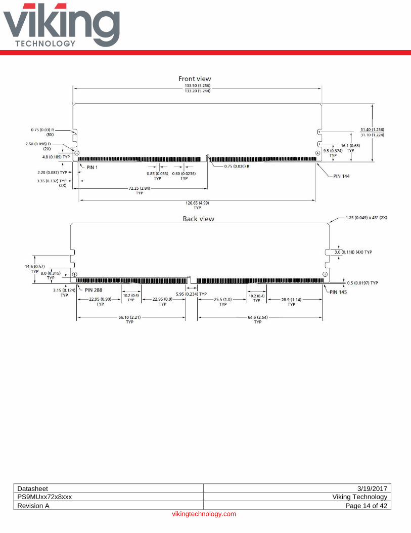
MECHANICAL OUTLINE
133.50 mm Max
31.4 mm
Max
3.90 mm
Max
1.50 mm
Max
Notes:
1. All dimensions in mm (inches) 2. Tolerance is +/- 0.0127, unless otherwise stated. 3. Refer to JEDEC Standard Mechanical Outline MO-309 for other details
4. DDR4 PCB is higher and thicker then DDR3 and the gold finger pins may have a ramp zone for easy insertion into DIMM Sockets
4.1mm
Datasheet 3/19/2017
PS9MUxx72x8xxx Viking Technology
Revision A Page 14 of 42
vikingtechnology.com
Datasheet 3/19/2017
PS9MUxx72x8xxx Viking Technology
Revision A Page 15 of 42
vikingtechnology.com
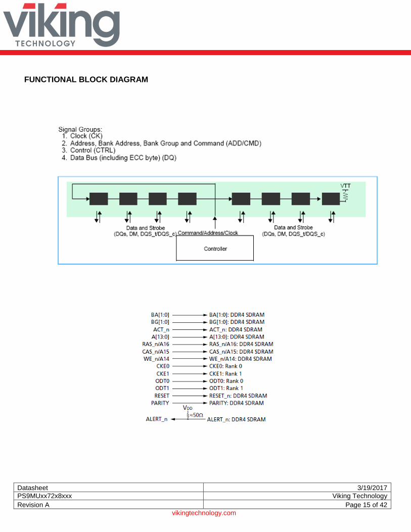
FUNCTIONAL BLOCK DIAGRAM

Datasheet 3/19/2017
PS9MUxx72x8xxx Viking Technology
Revision A Page 16 of 42
vikingtechnology.com
Notes:
The ZQ ball on each DDR4 component is connected to an external 240Ω ±1% resistor that is tied to ground. It is used for the calibration of
the component’s ODT and output driver.

Datasheet 3/19/2017
PS9MUxx72x8xxx Viking Technology
Revision A Page 17 of 42
vikingtechnology.com
DQ Internal Vref Specifications Parameter Symbol Min Typ Max Unit NOTE
Vref Max operating point Range 1 Vref_max_R1 - - 92% VDDQ 1, 11
Vref Min operating point Range 1 Vref_min_R1 60% - - VDDQ 1,11
Vref Max operating point Range 2 Vref_max_R2 - - 77% VDDQ 1, 11
Vref Min operating point Range 2 Vref_min_R2 45% - - VDDQ 1,11
Vref Stepsize Vref_step 0.50% 0.65% 0.80% VDDQ 2
Vref Set Tolerance Vref_set_tol -1 .625% 0.00% 1.63% VDDQ 3,4,6
-0.15% 0.00% 0.15% VDDQ 3,5,7
Vref Step Time Vref_time-long - - 150 ns 9
Vref_time-Short - - 60 ns 8
Vref VaIid tolerance Vref_val_tol -0.15% 0.00% 0.15% VDDQ 10 Notes: 1. JESD8-24 specifies Vref to be 70% of VDDQ. Vref DC voltage referenced to VDDQ_DC. VDDQ_DC is 1.2V 2. Vref stepsize increment/decrement range. Vref at DC level. 3. Vref_new = Vref_old+n*Vref_step; n=number of step; if increment use “+”; If decrement use “-” 4. The minimum value of Vref setting tolerance=Vref_new-1.625%*VDDQ.
The maximum value of Vref setting tolerance=Vref_new+1.625%*VDDQ. For n>4 5. The maximum value of Vref setting tolerance=Vref_new-0.15%*VDDQ.
The maximum value of Vref setting tolerance=Vref_new+0.15%*VDDQ. For n&4 tbd 6. Measured by recording the min and max values of the Vref output over the range, drawing a straight line between those points and comparing all
other Vref output settings to that line 7. Measured by recording the min and max values of the Vref output across 4 consecutive steps(n=4), drawing a straight line between those points
and comparing all other Vref output settings to that line 8. Time from MRS command to increment of decrement one step size for Vref 9. Time from MRS command to increment of decrement more than one step size up to full range of Vref 10. Only applicable for DRAM component level test/characterization purpose.
Not applicable for normal mode of operation. Vref valid is to qualify the step times which will be characterized at the component level.
11. DRAM range1 or 2 set by MRS bit MR6,A6.

Datasheet 3/19/2017
PS9MUxx72x8xxx Viking Technology
Revision A Page 18 of 42
vikingtechnology.com
OVERVIEW OF DDR4 UDIMM MODULE OPERATION The DDR4 architecture is generally a point-to-point topology with a dedicated channel design. The highest system performance levels can be achieved with DDR4-2133 and beyond, when the system is configured as 1 UDIMM Per Channel (1DPC). DDR4 has more features than DDR3 with a pseudo-open drain (POD12) 1.2v I/O for the data channel, trained Vref, bank groups and write CRC. The POD12 interface only applies to the data channel. The address command channel behave like DDR3 using mid-point termination and mid-point Vref. The new bank group interleaving feature in DDR4 maximizes data transfer bandwidth. DDR4 DRAM use pseudo-open drain (POD12) 1.2v drivers with Vdd terminations on DQ lines to increase data rates; unlike DDR3 DRAM that uses stub-series terminated logic drivers, The DRAM addressing scheme in DDR4 is organized into bank groups, Side A and Side B. The host DDR4 memory controller interleaves (multiplexes) among the bank groups to achieve high data rates. DDR4 architecture is a 8n prefetch with bank groups, including the use of two or four selectable bank groups. This will permit the DDR4 memory devices to have separate activation, read, write or refresh operations simultaneously underway in each of the unique bank groups to improve overall memory efficiency and bandwidth, especially when small memory granularities are used. The data written to the UDIMM is read back the same way. However when writing to the internal registers with a "load mode" operation, a specific address is required. This requires the controller to know if the rank is mirrored or not. There is a bit assignment in the SPD that indicates whether the module has been designed with a mirrored feature or not. DDR4 offers ECC recovery from command and parity errors to prevent the host system from crashing. The use of CRC parity is an optional feature on address command and data; (Error command blocking when parity enabled and post CA parity. If the UDIMM does not support CRC, the values of 0x00 will fill the CRC table. The new CA parity feature on the command/address bus provides a low-cost method of verifying the integrity of command and address transfers over a link, for all operations.
Some of the main attributes of DDR4 memory are: 1) Internally generated VrefDQ and Calibration.
VrefDQ is supplied by the DRAM internally. VrefCA is supplied by the board.
2) The ACT_n activate pin replaces RAS#, CAS#, and WE# commands, 3) Alert_n for error checking 4) Bank group Interleaving 5) Improved training modes upon power-up 5) Nominal and dynamic ODT: Improvements to the ODT protocol and a new Park Mode allow for a nominal termination
and dynamic write termination without having to drive the ODT pin 6) DQ bus geardown mode for 2667 Mhz data rates and beyond 7) External VPP at 2.5V (for wordline boost) 8) 1.2V VDD power with power-saving features that include MPSM Maximum Power Savings Mode, Low Power Auto Self
Refresh, Temperature Controlled Refresh, Fine Granularity Refresh, and CMD/ADDT latency. DLL off mode. Important Note: Longer boot-up times may be experienced in certain situations due to controller initiated functions such as VrefDQ calibration, write leveling and other trainings for the UDIMM.

Datasheet 3/19/2017
PS9MUxx72x8xxx Viking Technology
Revision A Page 19 of 42
vikingtechnology.com
DDR4 MODE REGISTERS A12 A11 A10 A9 A8 A7 A6 A5 A4 A3 A2 A1 A0
MR0 RFU Write Recovery and RTP DLL
Reset Test Mode
CAS Latency CL Burst Type
CL Burst Length BL
MR1 Qoff TDQS Rtt_NOM Write
Leveling RFU RFU Additive Latency Ron
DLL Enable
MR2 Write CRC
RFU Rtt_WR RFU Auto Self Refresh CWL RFU RFU RFU
MR3 MPR Read Format Write CMD Latency with CRC and DM
Fine Granularity Refresh Temp
Sensor
Per-DRAM Addr Mode
Gear down
MPR Enable
MPR Page
MR4 Write
Preamble Read
Preamble
Read Preamble Training Enable
Self Refresh Abort
Enable
CS-to-Address Latency CAL
RFU VrefDQ Monitor Enable
Temp Refresh Mode
Temp. Refresh Range
Max Power Down
Enable
RFU
MR5 Read DBI
Enable Write DBI
Enable
Data Mask
Enable
Parity Persistent Error
Rtt_PARK
ODT input
in Power Down
Panty Error
Status
CRC Error Clear
CMD Address Parity Latency
MR6 tCCD_L and tDLLK Timing RFU RFU VrefDQ Training enable
VrefDQ Training Range
VretDQ Training Value
MR7 Manufacturing use only to program the RCD
Notes:
Refer to JEDEC documentation for detail of the control/status bits

Datasheet 3/19/2017
PS9MUxx72x8xxx Viking Technology
Revision A Page 20 of 42
vikingtechnology.com
DC OPERATING CONDITIONS AND CHARACTERISTICS
ABSOLUTE MAXIMUM RATINGS
Parameter Symbol Value Unit Notes
Voltage on any pin relative to GND Vin, Vout -0.3 ~ 1.5 V 1,
Voltage on VDD supply relative to GND VDD -0.3 ~ 1.5 V 1,3
Voltage on VDDQ supply relative to GND VDDQ -0.3 ~ 1.5 V 1,3
Voltage on VPP supply relative to GND VPP -0.3 ~ 3.0 V 4
Module operating temperature (ambient) Topr 0 ~ 55 C 1,5
Storage temperature Tstg -55 ~ +100 C 1,2
Notes:
1. Permanent device damage may occur if ‘ABSOLUTE MAXIMUM RATINGS’ are exceeded. Functional operation should be restricted to recommended operating condition. Exposure to higher than recommended voltage for extended periods of time could affect device reliability. Stresses greater than those listed under “Absolute Maximum Ratings” may cause permanent damage to the device. This is a stress rating only and functional operation of the device at these or any other conditions above those indicated in the operational sections of this specification is not implied. Exposure to absolute maximum rating conditions for extended periods may affect reliability
2. Storage Temperature is the case surface temperature on the center/top side of the DRAM. For the measurement conditions, please refer to JESD51- 2 standard.
3. VDD and VDDQ must be within 300 mV of each other at all times and VREFCA must be not greater than 0.6 x VDDQ, When VDD and VDDQ are less than 500 mV; VREF may be equal to or less than 300 mV
4. VPP must be equal or greater than VDD/VDDQ at all times 5. Refer to JEDEC JC451 specification
DRAM Component Operating Temperature Range
Symbol Parameter Rating Units Note
Toper Normal Operating Temperature Range 0 to 85 °C 1,2
Extended Temperature Range 85 to 95 °C 1,3
Notes:
1. Operating Temperature TOPER is the case surface temperature on the center / top side of the DRAM. For measurement conditions, please refer to the JEDEC document JESD51-2.
2. The Normal Temperature Range specifies the temperatures where all DRAM specifications will be supported. During operation, the DRAM case temperature must be maintained between 0 - 85oC under all operating conditions. 3. Some applications require operation of the DRAM in the Extended Temperature Range between 85oC and 95oC case temperature. Full specifications are guaranteed in this range, but the following additional conditions apply: a) Refresh commands must be doubled in frequency, therefore reducing the Refresh interval tREFI to 3.9 µs. It is also possible to
specify a component with 1X refresh (tREFI to 7.8µs) in the Extended Temperature Range. Please refer to the DIMM SPD for option availability.
b) If Self-Refresh operation is required in the Extended Temperature Range, then it is mandatory to either use the Manual Self- Refresh mode with Extended Temperature Range capability (MR2 A6 = 0b and MR2 A7 = 1b) or enable the optional Auto Self-Refresh mode (MR2 A6 = 1b and MR2 A7 = 0b). DDR4 SDRAMs support Auto Self-Refresh and in Extended Temperature Range and please refer to component datasheet and/or the DIMM SPD for tREFI requirements in the Extended Temperature Range
tREFI by Device Density
Parameter Symbol 2Gb 4Gb 8Gb 16Gb Units
Average periodic refresh interval
tREFI
0°C ≤ Tcase ≤ 85°C 7.8 7.8 7.8 7.8 μs
85°C ≤ Tcase ≤ 95°C 3.9 3.9 3.9 3.9 μs

Datasheet 3/19/2017
PS9MUxx72x8xxx Viking Technology
Revision A Page 21 of 42
vikingtechnology.com
AC & DC Operating Conditions
DC OPERATING CONDITIONS AND CHARACTERISTICS (POD12)
Symbol Parameter Rating
Units Notes
Min Typ Max
VDD Supply Voltage VDD: PC4:1.2V±5%,
1.14 1.2 1.26 v 1,2,3
VDDQ Supply Voltage for Output. Values in () are at 70% of VDD
1.14 (0.798)
1.2 (0.84)
1.26 (0.882)
v 1
VPP 2.5V +10%, -5% 2.375 2.5 2.75 v 3
VDDSPD @2.5V 2.2 2.5 2.8 v
Notes:
1. JESD8-24 specifies Vref to be 70% of VDDQ. Under all conditions VDDQ must be less than or equal to VDD.
2. VDDQ tracks with VDD. AC parameters are measured with VDD and VDDQ tied together.
3. DC bandwidth is limited to 20MHz.,
4. PODI2 1.2 V Pseudo Open Drain Interface has a VDDQ value of 1.2V but the reference voltage allows PODI2 to be used with other VDDQ values. POD12 signals have pull-up-only parallel input termination and have an asymmetric output drive impedance. For example, if the output drivers were using a 60 ohm pull-up drive impedance then the pull-down drivers would be expected to produce a 40 ohm pull-down drive impedance. PODI2 does not explicitly call for series termination resistors, so it is suitable for point-to-point as well as multi-drop stub environments which may require some additional termination.

Datasheet 3/19/2017
PS9MUxx72x8xxx Viking Technology
Revision A Page 22 of 42
vikingtechnology.com
DC CHARACTERISTICS, IDD CURRENTS IDD DEFINITIONS
Symbol Parameter
IDD0 One bank ACTIVATE-PRECHARGE current
IPP0 One bank ACTIVATE-PRECHARGE, Word Line Boost, IPP current
IDD1 One bank ACTIVATE-READ-PRECHARGE current
IDD2N Precharge standby current
IDD2NT Precharge standby ODT current
IDD2P Precharge power-down current
IDD2Q Precharge quiet standby current
IDD3N Active standby current
IPP3N Active standby IPP current
IDD3P Active power-down current
IDD4R Burst read current
IDDQ4R Burst read IDDQ current
IDD4W Burst write current
IDD5B Burst refresh current (1x REF)
IPP5B Burst refresh IPP current (1 x REF)
IDD6N Self refresh current: Normal temperature range (0°C to +85°C)
IDD6E Self refresh current: Extended temperature range (0°C to +95°C)
IDD6R Self refresh current: Reduced temperature range (0°C to +45°C)
IDD6A Auto self refresh current (25°C)
IDD6A Auto self refresh current (45°C)
IDD6A Auto self refresh current (75°C)
IDD7 Bank interleave read current
IPP7 Bank interleave read IPP current
IDD8 Maximum power-down current
Notes: 1) DDR4 IDD and IDDQ specs include the same DDR3 IDD and IDDQ specs with these exceptions:
a. IDD2P0 and IDD2P1 are replaced with a single IDD2P. There’s no longer any difference in power for the DLL because of better DLL power management inside the DRAM device without any benefit for using slow exit.
b. IDD6 is renamed IDD6N Self Refresh Current: Normal Temperature Range c. IDD6ET is renamed IDD6E Self-Refresh Current: Extended Temperature Range d. IDD6TC is renamed IDD6AAut0 Self-Refresh Current e. IDD8 is redefined from (optional) RESET Low Current to IDD8 Maximum Power Down Current, TBD
2) IDD values are an average (not peak) current drawn throughout the entire time that it takes to execute the set of conditions specified by JEDEC standards.
3) Consult with Viking for tools to help specify the Total Design Power (TDP)

Datasheet 3/19/2017
PS9MUxx72x8xxx Viking Technology
Revision A Page 23 of 42
vikingtechnology.com
IDD6 Specification
Symbol Temperature Range Value Unit Notes
IDD6N 0 - 85 oC 22 mA 3,4
IDD6E 0 - 95 oC 33 mA 4,5,6
IDD6R 0 - 45oC 10 mA 4,6,9
IDD6A
0 oC ~ Ta 9 mA 4,6,7,8
Tb ~ Ty 10 mA 4,6,7,8
Tz ~ TOPERmax 16 mA 4,6,7,8 Notes: 1. Some IDD currents are higher for x16 organization due to larger page-size architecture. 2. Max. values for IDD currents considering worst case conditions of process, temperature and voltage. 3. Applicable for MR2 settings A6=0 and A7=0. 4. Supplier data sheets include a max value for IDD6. 5. Applicable for MR2 settings A6=0 and A7=1. IDD6ET is only specified for devices which support the Extended Temperature Range feature. 6. Refer to the supplier data sheet for the value specification method (e.g. max, typical) for IDD6ET and IDD6TC 7. Applicable for MR2 settings A6=1 and A7=0. IDD6TC is only specified for devices which support the Auto Self Refresh feature. 8. The number of discrete temperature ranges supported and the associated Ta - Tz values are supplier/design specific. Temperature ranges are specified for all supported values of TOPER. Refer to supplier data sheet for more information. 9. Applicable for MR2 settings TBD. IDD6R is verified by design and characterization, and may not be subject to production test.

Datasheet 3/19/2017
PS9MUxx72x8xxx Viking Technology
Revision A Page 24 of 42
vikingtechnology.com
IDD CURRENTS, SINGLE RANK, 4Gbit Symbol DDR4-1866 DDR4-2133 DDR4-2400 Units
IDD0 522 540 576 mA
IPP0 36 36 36 mA
IDD1 567 585 612 mA
IDD2N 396 414 450 mA
IDD2NT 450 486 522 mA
IDD2P 270 270 288 mA
IDD2Q 351 351 369 mA
IDD3N 549 567 603 mA
IPP3N 27 27 27 mA
IDD3P 396 396 396 mA
IDD4R 1260 1350 1440 mA
IDDQ4R 288 324 360 mA
IDD4W 1404 1584 1764 mA
IDD5B 1710 1710 1728 mA
IPP5B 198 198 198 mA
IDD6N 180 180 180 mA
IDD6E 243 243 243 mA
IDD6R 90 90 90 mA
IDD6A (25°C) 81 81 81 mA
IDD6A (45°C) 90 90 90 mA
IDD6A (75°C) 144 144 144 mA
IDD7 1440 1665 1890 mA
IPP7 90 108 126 mA
IDD8 162 162 162 mA
Notes:
1. Users should refer to the DRAM supplier data sheet and/or the DIMM SPD to determine if DDR4 SDRAM devices support the following options or requirements referred to in this material.
2. Values as per Micron Datasheet Revision “A”.

Datasheet 3/19/2017
PS9MUxx72x8xxx Viking Technology
Revision A Page 25 of 42
vikingtechnology.com
IDD CURRENTS, 2 RANK, 4Gbit
Symbol DDR4-1866 DDR4-2133 DDR4-2400 Units
IDD01 792 810 864 mA
IPP01 306 306 324 mA
IDD11 837 855 900 mA
IDD2N2 792 828 900 mA
IDD2NT1 720 756 810 mA
IDD2P2 540 540 576 mA
IDD2Q2 702 702 738 mA
IDD3N2 1098 1134 1206 mA
IPP3N2 54 54 54 mA
IDD3P2 792 792 792 mA
IDD4R1 1530 1620 1728 mA
IDDQ4R1 558 594 648 mA
IDD4W1 1674 1854 2052 mA
IDD5B1 1980 1980 2016 mA
IPP5B1 468 468 468 mA
IDD6N2 360 360 360 mA
IDD6E2 486 486 486 mA
IDD6R2 180 180 180 mA
IDD6A2 (25°C) 162 162 162 mA
IDD6A2 (45°C) 180 180 180 mA
IDD6A2 (75°C) 288 288 288 mA
IDD71 1710 1935 2178 mA
IPP71 360 378 414 mA
IDD82 324 324 324 mA
Notes: 1. One module rank in the active IDD/PP, the other rank in IDD2P/PP3N. 2. All ranks in this IDD/PP condition. 3. Values as per Micron Datasheet Revision “A.

Datasheet 3/19/2017
PS9MUxx72x8xxx Viking Technology
Revision A Page 26 of 42
vikingtechnology.com
IDD CURRENTS, SINGLE RANK, 8Gbit
Symbol
DDR4-2133 DDR4-2400 Units
15-15-15 17-17-17
1.2V 1.2V
IDD0 315 333 mA
IDD0A 333 351 mA
IDD1 450 477 mA
IDD1A 468 504 mA
IDD2N 198 207 mA
IDD2NA 225 234 mA
IDD2NT 225 234 mA
IDD2NL 135 153 mA
IDD2NG 198 207 mA
IDD2ND 180 189 mA
IDD2N_par 207 216 mA
IDD2P 144 144 mA
IDD2Q 180 189 mA
IDD3N 324 324 mA
IDD3NA 342 342 mA
IDD3P 189 198 mA
IDD4R 927 1017 mA
IDD4RA 963 1062 mA
IDD4RB 945 1044 mA
IDD4W 756 810 mA
IDD4WA 792 855 mA
IDD4WB 846 810 mA
IDD4WC 666 720 mA
IDD4W_par 828 891 mA
IDD5B 1971 1998 mA
IDD5F2 1386 1395 mA
IDD5F4 1152 1170 mA
IDD6N 207 207 mA
IDD6E 306 306 mA
IDD7 1530 1557 mA
IDD8 99 99 mA Notes:
1. Users should refer to the DRAM supplier data sheet and/or the DIMM SPD to determine if DDR4 SDRAM devices support the following options or requirements referred to in this material.
2. Samsung D – Die referred for Idd values.

Datasheet 3/19/2017
PS9MUxx72x8xxx Viking Technology
Revision A Page 27 of 42
vikingtechnology.com
IDD CURRENTS, DUAL RANK, 8Gbit
Symbol
DDR4-2133 DDR4-2400 Units
15-15-15 17-17-17
1.2V 1.2V
IDD01 459 477 mA
IDD0A1 477 495 mA
IDD11 594 621 mA
IDD1A1 612 648 mA
IDD2N2 396 414 mA
IDD2NA1 369 378 mA
IDD2NT1 369 378 mA
IDD2NL1 279 297 mA
IDD2NG1 342 351 mA
IDD2ND1 324 333 mA
IDD2N_par1 351 360 mA
IDD2P2 288 288 mA
IDD2Q2 360 378 mA
IDD3N2 648 648 mA
IDD3NA2 684 684 mA
IDD3P2 378 396 mA
IDD4R1 1071 1161 mA
IDD4RA1 1107 1206 mA
IDD4RB1 1089 1188 mA
IDD4W1 900 954 mA
IDD4WA1 936 999 mA
IDD4WB1 990 954 mA
IDD4WC1 810 864 mA
IDD4W_par1 972 1035 mA
IDD5B1 2115 2142 mA
IDD5F21 1530 1539 mA
IDD5F41 1296 1314 mA
IDD6N2 414 414 mA
IDD6E2 612 612 mA
IDD71 1674 1701 mA
IDD82 198 198 mA
Notes: 1. One module rank in the active IDD/PP, the other rank in IDD2P/PP3N. 2. All ranks in this IDD/PP condition. 3. Users should refer to the DRAM supplier data sheet and/or the DIMM SPD to determine if DDR4 SDRAM devices support the following options or requirements referred to in this material. 4. Samsung D – Die referred for Idd values. .
Datasheet 3/19/2017
PS9MUxx72x8xxx Viking Technology
Revision A Page 28 of 42
vikingtechnology.com
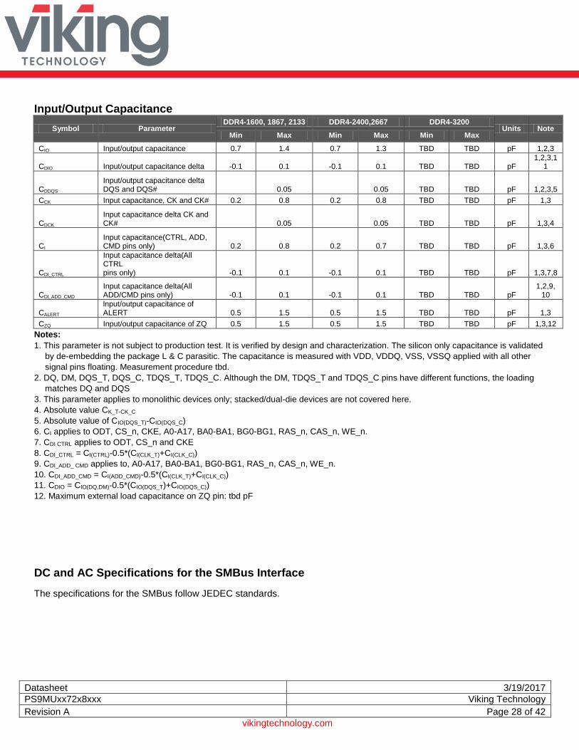
Input/Output Capacitance
Symbol Parameter DDR4-1600, 1867, 2133 DDR4-2400,2667 DDR4-3200
Units Note Min Max Min Max Min Max
CIO Input/output capacitance 0.7 1.4 0.7 1.3 TBD TBD pF 1,2,3
CDIO Input/output capacitance delta -0.1 0.1 -0.1 0.1 TBD TBD pF 1,2,3,1
1
CDDQS Input/output capacitance delta DQS and DQS# 0.05 0.05 TBD TBD pF 1,2,3,5
CCK Input capacitance, CK and CK# 0.2 0.8 0.2 0.8 TBD TBD pF 1,3
CDCK Input capacitance delta CK and CK# 0.05 0.05 TBD TBD pF 1,3,4
CI Input capacitance(CTRL, ADD, CMD pins only) 0.2 0.8 0.2 0.7 TBD TBD pF 1,3,6
CDI_CTRL
Input capacitance delta(All CTRL pins only) -0.1 0.1 -0.1 0.1 TBD TBD pF 1,3,7,8
CDl_ADD_CMD Input capacitance delta(All ADD/CMD pins only) -0.1 0.1 -0.1 0.1 TBD TBD pF
1,2,9, 10
CALERT lnput/output capacitance of ALERT 0.5 1.5 0.5 1.5 TBD TBD pF 1,3
CZQ Input/output capacitance of ZQ 0.5 1.5 0.5 1.5 TBD TBD pF 1,3,12
Notes:
1. This parameter is not subject to production test. It is verified by design and characterization. The silicon only capacitance is validated
by de-embedding the package L & C parasitic. The capacitance is measured with VDD, VDDQ, VSS, VSSQ applied with all other
signal pins floating. Measurement procedure tbd.
2. DQ, DM, DQS_T, DQS_C, TDQS_T, TDQS_C. Although the DM, TDQS_T and TDQS_C pins have different functions, the loading
matches DQ and DQS
3. This parameter applies to monolithic devices only; stacked/dual-die devices are not covered here.
4. Absolute value CK_T-CK_C
5. Absolute value of CIO(DQS_T)-CIO(DQS_C)
6. CI applies to ODT, CS_n, CKE, A0-A17, BA0-BA1, BG0-BG1, RAS_n, CAS_n, WE_n.
7. CDI CTRL applies to ODT, CS_n and CKE
8. CDI_CTRL = CI(CTRL)-0.5*(CI(CLK_T)+CI(CLK_C))
9. CDI_ADD_ CMD applies to, A0-A17, BA0-BA1, BG0-BG1, RAS_n, CAS_n, WE_n.
10. CDI_ADD_CMD = CI(ADD_CMD)-0.5*(CI(CLK_T)+CI(CLK_C))
11. CDIO = CIO(DQ,DM)-0.5*(CIO(DQS_T)+CIO(DQS_C))
12. Maximum external load capacitance on ZQ pin: tbd pF
DC and AC Specifications for the SMBus Interface
The specifications for the SMBus follow JEDEC standards.

Datasheet 3/19/2017
PS9MUxx72x8xxx Viking Technology
Revision A Page 29 of 42
vikingtechnology.com
Speed Bins by Speed Grade DDR4-1600 Speed Bins and Operating Conditions
Speed Bin DDR4-1600
Unit NOTE CL-nRCD-nRP 11-11-11
Parameter Symbol Min Max
Internal read command to first data tAA 13.75
14
(13.50)5,12
18 ns
Internal read command to first data with read DBI enabled
tAA_DBI tAA(min) +
2nCK tAA(max) +2nCK
ns
ACT to internal read or write delay time tRCD 13.75
(13.50)5,12
- ns
PRE command period tRP 13.75
(13.50)5,12
- ns
ACT to PRE command period tRAS 35 9 x tREFI ns
ACT to ACT or REF command period tRC 48.75
(48.50)5,12
- ns
Normal Read DBI
CWL = 9 CL = 9
CL = 11 (Optional)
5
tCK(AVG) Reserved ns 1,2,3,4,11
,14
CL = 10 CL = 12 tCK(AVG) 1.5 1.6 ns 1,2,3,4,11
CWL = 9,11
CL = 10 CL = 12 tCK(AVG) Reserved ns 1,2,3,4
CL = 11 CL = 13 tCK(AVG) 1.25 <1.5 ns 1,2,3,4
CL = 12 CL = 14 tCK(AVG) 1.25 <1.5 ns 1,2,3
Supported CL Settings (9),11,12 nCK 13,14
Supported CL Settings with read DBI (11),13,14 nCK 13
Supported CWL Settings 9,11 nCK

Datasheet 3/19/2017
PS9MUxx72x8xxx Viking Technology
Revision A Page 30 of 42
vikingtechnology.com
DDR4-1866 Speed Bins and Operating Conditions
Speed Bin DDR4-1866
Unit NOTE CL-nRCD-nRP 13-13-13
Parameter Symbol Min Max
Internal read command to first data tAA 13.9214
(13.50)5,12
18 ns
Internal read command to first data with read DBI enabled
tAA_DBI tAA(min) + 2nCK tAA(max) +2nCK
ns
ACT to internal read or write delay time
tRCD 13.92 (13.50)5,12 - ns
PRE command period tRP 13.92 (13.50)5,12
- ns
ACT to PRE command period tRAS 34 9 x tREFI ns
ACT to ACT or REF command period
tRC 47.92 (47.50)5,12
- ns
Normal Read DBI
CWL=9
CL=9 CL=11
(Optional)5
tCK(AVG) Reserved ns 1,2,3,4,11
,14
CL=10 CL=12 tCK(AVG) 1.5 1.6 ns 1,2,3,4,11
CWL=9,11
CL=10 CL=12 tCK(AVG) 4
CL=11 CL=13 tCK(AVG)
1.25 <1.5 ns 1,2,3,4,6
(Optional)5,12
CL=12 CL=14 tCK(AVG) 1.25 <1.5 ns 1,2,3,6
CWL=10,12
CL=12 CL=14 tCK(AVG) Reserved ns 1,2,3,4
CL=13 CL=15 tCK(AVG) 1.071 <1.25 ns 1,2,3,4
CL=14 CL=16 tCK(AVG) 1.071 <1.25 ns 1,2,3
Supported CL Settings 9,11,12,13,14 nCK 13,14
Supported CL Settings with read DBI 11,13,14 ,15,16 nCK 13
Supported CWL Settings 9,10,11,12 nCK

Datasheet 3/19/2017
PS9MUxx72x8xxx Viking Technology
Revision A Page 31 of 42
vikingtechnology.com
DDR4-2133 Speed Bins and Operating Conditions
Speed Bin DDR4-2133
Unit NOTE CL-nRCD-nRP 15-15-15
Parameter Symbol Min Max
Internal read command to first data tAA 14.0614
(13.75)5,12
18 ns
Internal read command to first data with read DBI enabled
tAA_DBI tAA(min) + 3nCK tAA(max) + 3nCK
ns
ACT to internal read or write delay time
tRCD 14.06 (13.75)5,12
- ns
PRE command period tRP 14.06 (13.75)5,12
- ns
ACT to PRE command period tRAS 33 9 x tREFI ns
ACT to ACT or REF command period tRC 47.06 (46.75)
5,12 - ns
Normal Read DBI
CWL = 9
CL = 9 CL = 11
(Optional)5
tCK(AVG)
Reserved
ns 1,2,3,4,11,
14
CL = 10 CL = 12 tCK(AVG) 1.5 1.6 ns 1,2,3,11
CWL = 9,11
CL = 11 CL = 13
tCK(AVG) ns 1,2,3,4,7
tCK(AVG) (Optional)5,12
CL = 12 CL = 14 tCK(AVG) 1.25 <1.5 ns 1,2,3,7
CWL = 10,12
CL = 13 CL = 15
tCK(AVG) 1.071 <1.25 ns 1,2,3,4,7
tCK(AVG) (Optional)5,12
CL = 14 CL = 16 tCK(AVG) 1.071 <1.25 ns 1,2,3,7
CWL = 11,14
CL = 14 CL = TBD tCK(AVG) Reserved ns 1,2,3,4
CL = 15 CL = TBD tCK(AVG) 0.937 <1.071 ns 1,2,3,4
CL = 16 CL = TBD tCK(AVG) 0.937 <1.071 ns 1,2,3
Supported CL Settings (9),(11),12,(13),14,15,16 nCK 13,14
Supported CL Settings with read DBI (11),(13),14,(15),16,18,19 nCK
Supported CWL Settings 9,10,11,12,14 nCK

Datasheet 3/19/2017
PS9MUxx72x8xxx Viking Technology
Revision A Page 32 of 42
vikingtechnology.com
DDR4-2400 Speed Bins and Operating Conditions
Speed Bin DDR4-2400
Unit NOTE CL-nRCD-nRP 17-17-17
Parameter Symbol Min Max
Internal read command to first data tAA 14.1614
(13.75)5,12
18 ns
Internal read command to first data with read DBI enabled
tAA_DBI tAA(min) + 3nCK tAA(max) + 3nCK
ns
ACT to internal read or write delay time
tRCD 14.16 (13.75)5,12
- ns
PRE command period tRP 14.16 (13.75)5,12
- ns
ACT to PRE command period tRAS 32 9 x tREFI ns
ACT to ACT or REF command period tRC 46.16 (45.75)
5,12 - ns
Normal Read DBI
CWL = 9 CL = 9
CL = 11 (Optional)
5
tCK(AVG)
Reserved ns
1,2,3,4,11, 14
CL = 10 CL = 12 tCK(AVG) 1.5 1.6 ns 1,2,3,11
CWL = 9,11
CL = 11 CL = 13
tCK(AVG) ns 1,2,3,4,7
tCK(AVG) (Optional)5,12
CL = 12 CL = 14 tCK(AVG) 1.25 <1.5 ns 1,2,3,7
CWL = 10,12
CL = 13 CL = 15
tCK(AVG) 1.071 <1.25 ns 1,2,3,4,7
tCK(AVG) (Optional)5,12
CL = 14 CL = 16 tCK(AVG) 1.071 <1.25 ns 1,2,3,7
CWL = 11,14
CL = 14 CL = 17 tCK(AVG) Reserved ns 1,2,3,4
CL = 15 CL = 18 tCK(AVG) 0.938 <1.071 ns 1,2,3,4
CL = 16 CL = 19 tCK(AVG) 0.938 <1.071 ns 1,2,3
CWL = 12,16
CL = 15 CL = 18 tCK(AVG) Reserved ns 1,2,3,4
CL = 16 CL = 19 tCK(AVG) Reserved ns 1,2,3,4
CL = 17 CL = 20 tCK(AVG) 0.833 <0.938 ns 1,2,3
CL = 18 CL = 21 tCK(AVG) 0.833 <0.938 ns 1,2,3,4
Supported CL Settings (10),(11),12,(13),14,15,16,17,18 nCK 13,14
Supported CL Settings with read DBI (12),(13),14,(15),16,18,19,20,21 nCK
Supported CWL Settings 9,10,11,12,14,16 nCK

Datasheet 3/19/2017
PS9MUxx72x8xxx Viking Technology
Revision A Page 33 of 42
vikingtechnology.com
DDR4-2666 Speed Bins and Operating Conditions
Speed Bin DDR4-2666
Unit NOTE CL-nRCD-nRP 22-19-19
Parameter Symbol Min Max
Internal read command to first data tAA 16.5 21.5 ns
ACT to internal read or write delay time tRCD 14.25 - ns
PRE command period tRP 14.25 - ns
ACT to PRE command period tRAS 32 9 x tREFI ns
ACT to ACT or REF command period tRC 46.25 - ns
CWL = 9,11 CL = 13 tCK(AVG) Reserved ns 1,2,3,4,9
CL = 14 tCK(AVG) 1.25 1.5 ns 1,2,3,8
CWL = 10,12 CL = 14 tCK(AVG) Reserved ns 1,2,3,4,9
CL = 15 tCK(AVG) Reserved ns 1,2,3,4,9
CL = 16 tCK(AVG) 1.071 <1.25 ns 1,2,3,9
CWL = 11,14 CL = 16 tCK(AVG) Reserved ns 1,2,3,4,9
CL = 18 tCK(AVG) 0.937 <1.071 ns 1,2,3,4,9
CL = 20 tCK(AVG) 0.937 <1.071 ns 1,2,3,9
CWL = 12,16 CL = 18 tCK(AVG) Reserved ns 1,2,3,4,9
CL = 20 tCK(AVG) 0.833 <0.937 ns 1,2,3,4,9
CL = 22 tCK(AVG) 0.833 <0.937 ns 1,2,3,9
CWL = 14,18 CL = 20 tCK(AVG) Reserved ns 1,2,3,4,9
CL = 22 tCK(AVG) 0.75 0.833 ns 1,2,3,4,9
CL = 24 tCK(AVG) 0.75 0.833 ns 1,2,3,9
Supported CL Settings 11,12,13,14,15,16,17,18,19,20,22,24 nCK
Supported nRCD Timings minimum 12 nCK
Supported nRP Timings minimum 12 nCK
Supported CWL Settings 9,10,11,12,14,16,18 nCK
Timing Parameters by Speed Grade
Speed DDR4-1600 DDR4-1866 DDR4-2133 Units Note
Parameter Symbol MIN MAX MIN MAX MIN MAX
Clock Timing
Minimum Clock Cycle Time (DLL off mode)
tCK(DLL_OFF) 8 - 8 - 8 - ns 23
Average Clock Period tCK(avg) See Speed Bins Table ps
Average high pulse width tCH(avg) 0.48 0.52 0.48 0.52 0.48 0.52 tCK(avg)
Average low pulse width tCL(avg) 0.48 0.52 0.48 0.52 0.48 0.52 tCK(avg)
Absolute Clock Period tCK(abs) tCK(avg)min +
tJIT(per)min_tot tCK(avg)max +
tJIT(per)max_tot tCK(avg)min +
tJIT(per)min_tot tCK(avg)max +
tJIT(per)max_tot tCK(avg)min +
tJIT(per)min_tot tCK(avg)max +
tJIT(per)max_tot tCK
Absolute clock HIGH pulse width
tCH(abs) 0.45 - 0.45 - 0.45 - tCK(avg) 24

Datasheet 3/19/2017
PS9MUxx72x8xxx Viking Technology
Revision A Page 34 of 42
vikingtechnology.com
Speed DDR4-1600 DDR4-1866 DDR4-2133 Units Note
Parameter Symbol MIN MAX MIN MAX MIN MAX
Absolute clock Low pulse width
tCL(abs) 0.45 - 0.45 - 0.45 - tCK(avg) 25
Clock Period Jitter- total JIT(per)_tot -0.1 0.1 -0.1 0.1 -0.1 0.1 UI 26
Clock Period Jitter- deterministic
JIT(per)_dj tbd UI 27
Clock Period Jitter during DLL locking period
tJIT(per, lck) tbd UI
Cycle to Cycle Period Jitter tJIT(cc)_tot 0.2 0.2 0.2 UI 26
Cycle to Cycle Period Jitter- deterministic
tJIT(cc)_dj tbd UI 27
Cycle to Cycle Period Jitter during DLL locking period
tJIT(cc, lck) tbd UI
Duty cycle Jitter tJIT(duty) tbd UI
Cumulative error across 2 cycles
tERR(2per) tbd UI
Cumulative error across 3 cycles
tERR(3per) tbd UI
Cumulative error across 4 cycles
tERR(4per) tbd UI
Cumulative error across 5 cycles
tERR(5per) tbd UI
Cumulative error across 6 cycles
tERR(6per) tbd UI
Cumulative error across 7 cycles
tERR(7per) tbd UI
Cumulative error across 8 cycles
tERR(8per) tbd UI
Cumulative error across 9 cycles
tERR(9per) tbd UI
Cumulative error across 10 cycles
tERR(10per) tbd UI
Cumulative error across 11 cycles
tERR(11per) tbd UI
Cumulative error across 12 cycles
tERR(12per) tbd UI
Cumulative error across n = 13, 14 ... 49, 50 cycles
tERR(nper) tbd UI
Command and Address Timing
CAS_n to CAS_n command delay for same bank group
tCCD_L 5 - 5 - 6 - nCK
CAS_n to CAS_n command delay for different bank group
tCCD_S 4 - 4 - 4 - nCK
ACTIVATE to ACTIVATE Command delay to different bank group for 2KB page size
tRRD_S(2K) Max(4nCK,6ns) - Max(4nCK,5.3ns) - Max(4nCK,5.3ns) - nCK
ACTIVATE to ACTIVATE Command delay to different bank group for 1KB page size
tRRD_S(1K) Max(4nCK,5ns) - Max(4nCK,4.2ns) - Max(4nCK,3.7ns) - nCK
ACTIVATE to ACTIVATE Command delay to different bank group for 1/2KB page size
tRRD_S(1/2K) Max(4nCK,5ns) - Max(4nCK,4.2ns) - Max(4nCK,3.7ns) - nCK
ACTIVATE to ACTIVATE Command delay to same bank group for 2KB page size
tRRD_L(2K) Max(4nCK,7.5ns) - Max(4nCK,6.4ns) - Max(4nCK,6.4ns) - nCK
ACTIVATE to ACTIVATE Command delay to same bank group for 1KB page size
tRRD_L(1K) Max(4nCK,6ns) - Max(4nCK,5.3ns) - Max(4nCK,5.3ns) - nCK
ACTIVATE to ACTIVATE Command delay to same bank group for 1/KB page size
tRRD_L(1/2K) Max(4nCK,6ns) - Max(4nCK,5.3ns) - Max(4nCK,5.3ns) - nCK
Four activate window for 2KB page size
tFAW_2K 35 30 30 ns
Four activate window for 1KB page size
tFAW _1K 25 23 21 ns
Four activate window for 1KB page size
tFAW _1/2K 20 17 15 ns
Delay from start of internal write transaction to internal read command for different bank group
tWTR_S max(2nCK,2.5ns) - max(2nCK,2.5ns) - max(2nCK,2.5ns) - 1,2,e
Delay from start of internal write transaction to internal read command for same bank group
tWTR_L max(4nCK,7.5ns) - max(4nCK,7.5ns) - max(4nCK,7.5ns) - 1
Internal READ Command to PRECHARGE Command delay
tRTP max (4nCK,7.5ns) - max (4nCK,7.5ns) - max (4nCK,7.5ns) -
WRITE recovery time tWR 15 - 15 - 15 - ns 1

Datasheet 3/19/2017
PS9MUxx72x8xxx Viking Technology
Revision A Page 35 of 42
vikingtechnology.com
Speed DDR4-1600 DDR4-1866 DDR4-2133 Units Note
Parameter Symbol MIN MAX MIN MAX MIN MAX
WRITE recovery time when CRC and DM are enabled
tWR_CRC_DM tWR+max(4nCK,3.75ns) - tWR+max(5nCK,3.75ns) - tWR+max(5nCK,3.75ns) - ns 1,29
Delay from start of internal write transaction to internal read command for different bank groups with both CRC and OM enabled
tWTR_S_ CRC_DM
tWTR_S+max(4nCK,3.75ns) - tWTR_S+max(5nCK,3.75ns) - tWTR_S+max(5nCK,3.75ns) - ns 2,30
Delay from start of internal write transaction to internal read command for same bank group with both CRC and OM enabled
tWTR_L_ CRC_DM
tWTR_L+max(4nCK,3.75ns) - tWTR_L+max(5nCK,3.75ns) - tWTR_L+max(5nCK,3.75ns) - ns 3,31
DLL locking time tDLLK TBD nCK
Mode Register Set command cycle time
tMRD 8 - 8 - 8 - nCK
Mode Register Set command update delay
tMOD max(24nCK,15ns) - max(24nCK,15ns) - max(24nCK,15ns) -
Multi-Purpose Register Recovery Time
tMPRR 1 - 1 - 1 - nCK
Multi-Purpose Register Write Recovery Time
tWR_MPR tMOD (min) - tMOD (min) - tMOD (min) -
CS_n to Command Address Latency
CS_n to Command Address Latency
tCAL 3 - 4 - 4 - nCK
DRAM Data Timing
DQS_t,DQS_c to DQ skew, per group, per access
tDQSQ - tbd - tbd - tbd tCK(avg)/2 14,1,
9
DQS_t,DQS_c to DQ skew deterministic, per group, per access
tDQSQ - tbd - tbd - tbd tCK(avg)/2 15,1,7,19
DQ output hold time from DQS_t,DQS_c
tQH tbd - - - tCK(avg)/2 14,1,8,19
DQ output hold time deterministic from DQS_t, DQS_c
tQH tbd - - - UI 15,1,7,19
DQS_t,DQS_c to DQ Skew total, per group, per access; DBI enabled
tDQSQ - tbd - tbd - tbd UI 14,20
DQ output hold time total from DQS_t, DQS_c; DBI enabled
tQH TBD - TBD - TBD - UI 14,20
DQ to DQ offset , per group, per access refer-enced to DQS_t, DQS_c
tDQSQ TBD TBD TBD TBD TBD TBD UI 16, 17
Data Strobe Timing
DQS_t,DQS_c differential output high time
tQSH TBD TBD TBD TBD TBD TBD tCK(avg)/2 22
DQS_t,DQS_c differential output low time
tQSL TBD TBD TBD TBD TBD TBD tCK(avg)/2 21
MPSM Timing
Command path disable delay upon MPSM entry
tMPED tMOD(min) + tCPDED(min) - tMOD(min) + tCPDED(min) - tMOD(min) + tCPDED(min) -
Valid clock requirement after MPSM entry
tCKMPE tMOD(min) + tCPDED(min) - tMOD(min) + tCPDED(min) - tMOD(min) + tCPDED(min) -
Valid clock requirement before MPSM exit
tCKMPX tCKSRX(min) - tCKSRX(min) - tCKSRX(min) -
Exit MPSM to commands not requiring a locked DLL
tXMP TBD - TBD - TBD -
Exit MPSM to commands requiring a locked DLL
tXMPDLL tXMP(min) + tXSDLL(min) - tXMP(min) + tXSDLL(min) - tXMP(min) + tXSDLL(min) -
CS setup time to CKE tMPX_S TBD - TBD - TBD -
CS hold time to CKE tMPX_H TBD - TBD - TBD -
Calibration Timing
Power-up and RESET calibration time
tZQinit 1024 - 1024 - 1024 - nCK
Normal operation Full calibration time
tZQoper 512 - 512 - 512 - nCK
Normal operation Short calibration time
tZQCS 128 - 128 - 128 - nCK
Reset/Self Refresh Timing
Exit Reset from CKE HIGH to a valid command
tXPR max (5nCK,tRFC(min) +
10ns) -
max (5nCK,tRFC(min) + 10ns)
- max (5nCK,tRFC(min) +
10ns) -
Exit Self Refresh to commands not requiring a locked DLL
tXS tRFC(min)+10ns - tRFC(min)+10ns - tRFC(min)+10ns -
SRX to commands not requiring a locked DLL in Self Refresh ABORT
tXS_ABORT(min) tRFC4(min)+10ns - tRFC4(min)+10ns - tRFC4(min)+10ns -

Datasheet 3/19/2017
PS9MUxx72x8xxx Viking Technology
Revision A Page 36 of 42
vikingtechnology.com
Speed DDR4-1600 DDR4-1866 DDR4-2133 Units Note
Parameter Symbol MIN MAX MIN MAX MIN MAX
Exit Self Refresh to ZQCL,ZQCS and MRS (CL,CWL,WR,RTP and Gear Down)
tXS_FAST (min) tRFC4(min)+10ns - tRFC4(min)+10ns - tRFC4(min)+10ns -
Exit Self Refresh to commands requiring a locked DLL
tXSDLL tDLLK(min) - tDLLK(min) - tDLLK(min) -
Minimum CKE low width for Self refresh entry to exit timing
tCKESR tCKE(min)+1nCK - tCKE(min)+1nCK - tCKE(min)+1nCK -
Valid Clock Requirement after Self Refresh Entry (SRE) or Power-Down Entry (PDE)
tCKSRE max(5nCK,10ns) - max(5nCK,10ns) - max(5nCK,10ns) -
Valid Clock Requirement after Self Refresh Entry (SRE) or Power-Down when CA Parity is enabled
tCKSRE_PAR max (5nCK,10ns)+PL - max (5nCK,10ns)+PL - max (5nCK,10ns)+PL -
Valid Clock Requirement before Self Refresh Exit (SRX) or Power-Down Exit (PDX) or Reset Exit
tCKSRX max(5nCK,10ns) - max(5nCK,10ns) - max(5nCK,10ns) -
Power Down Timing
Exit Power Down with DLL on to any valid command; Exit Precharge Power Down with DLL frozen t commands not requiring a locked DLL
tXP max (4nCK,6ns) - max (4nCK,6ns) - max (4nCK,6ns) -
Exit Precharge Power Down with DLL frozen to commands requiring a locked DLL
tXPDLL max (10nCK, 24ns) - max (10nCK, 24ns) - max (10nCK, 24ns) - 3
CKE minimum pulse width tCKE max (3nCK, 5ns) - max (3nCK, 5ns) - max (3nCK, 5ns) - 32,33
Command pass disable delay
tCPDED 4 - 4 - 4 -
Power Down Entry to Exit Timing
tPD tCKE(min) 9*tREFI tCKE(min) 9*tREFI tCKE(min) 9*tREFI 6
Timing of ACT command to Power Down entry
tACTPDEN 1 - 1 - 2 - 7
Timing of PRE or PREA command to Power Down entry
tPRPDEN 1 - 1 - 2 - 7
Timing of RD/RDA command to Power Down entry
tRDPDEN RL+4+1 - RL+4+1 - RL+4+1 - nCK
Timing of WR command to Power Down entry (BL8OTF, BL8MRS, BC4OTF)
tWRPDEN WL+4+(tWR/ tCK(avg)) - WL+4+(tWR/ tCK(avg)) - WL+4+(tWR/ tCK(avg)) - nCK 4
Timing of WRA command to Power Down entry (BL8OTF, BL8MRS, BC4OTF)
tWRAPDEN WL+4+WR+1 - WL+4+WR+1 - WL+4+WR+1 - nCK 5
Timing of WR command to Power Downentry (BC4MRS)
tWRPBC4DEN WL+2+(tWR/ tCK(avg)) - WL+2+(tWR/ tCK(avg)) - WL+2+(tWR/ tCK(avg)) - nCK 4
Timing of WRA command to Power Down entry (BC4MRS)
tWRAPBC4DEN WL+2+WR+1 - WL+2+WR+1 - WL+2+WR+1 - nCK 5
Timing of REF command to Power Down entry
tREFPDEN 1 - 1 - 2 - nCK 7,8
Timing of MRS command to Power Down entry
tMRSPDEN tMOD(min) - tMOD(min) - tMOD(min) -
PDA Timing
Mode Register Set command cycle time in PDA mode
tMRD_PDA max(16nCK,10ns) - max(16nCK,10ns) - max(16nCK,10ns) -
Mode Register Set command update delay in PDA mode
tMOD_PDA tMOD tMOD tMOD
ODT Timing
Asynchronous RTT turn-on delay (Power-Down with DLL frozen)
tAONAS 1 9 1 9 1 9 ns
Asynchronous RTT turn-off delay (Power-Down with DLL frozen)
tAOFAS 1 9 1 9 1 9 ns
RTT dynamic change skew tADC 0.3 0.7 0.3 0.7 0.3 0.7 tCK(avg)
Write Leveling Timing
First DQS_t/DQS_n rising edge after write leveling mode is programmed
tWLMRD 40 - 40 - 40 - nCK 13
DQS_t/DQS_n delay after write leveling mode is programmed
tWLDQSEN 25 - 25 - 25 - nCK 13
Write leveling setup time from rising CK_t, CK_c crossing to rising DQS_t/DQS_n crossing
tWLS 0.13 - 0.13 - 0.13 - tCK(avg)

Datasheet 3/19/2017
PS9MUxx72x8xxx Viking Technology
Revision A Page 37 of 42
vikingtechnology.com
Speed DDR4-1600 DDR4-1866 DDR4-2133 Units Note
Parameter Symbol MIN MAX MIN MAX MIN MAX
Write leveling hold time from rising DQS_t/DQS_n crossing to rising CK_t, CK_ crossing
tWLH 0.13 - 0.13 - 0.13 - tCK(avg)
Write leveling output delay tWLO 0 9.5 0 9.5 0 9.5 ns
Write leveling output error tWLOE ns
CA Parity Timing
Commands not guaranteed to be executed during this time
tPAR_UNKNOWN - Max(2nCK,3ns) - Max(2nCK,3ns) - Max(2nCK,3ns)
Delay from errant command to ALERT_n assertion
tPAR_ALERT_ON - PL+6ns - PL+6ns - PL+6ns
Pulse width of ALERT_n signal when asserted
tPAR_ALERT_PW 48 96 56 112 64 128 nCK
Time from when Alert is asserted till controller must start providing DES commands in Persistent CA parity mode
tPAR_ALERT_RSP - 43 - 50 - 57 nCK
Parity Latency [ 1715.64, JC42.3C]
PL 4 4 4 nCK
CRC Error Reporting
CRC error to ALERT_n latency
tCRC_ALERT - 13 - 13 - 13 ns
CRC ALERT_n pulse width CRC_ALERT_PW 6 10 6 10 6 10 nCK
Write recovery time when CRC and DM are enabled
tWR_CRC_DM tWR+max (4nCK,3.75ns) - tWR+max (5nCK,3.75ns) - tWR+max (5nCK,3.75ns) - ns 10
delay from start of internal write transaction to internal delay from start of internal write transaction to internal read command for different bank group with both CRC and DM enabled
tWTR_S_C RC_DM
tWTR_S+max (4nCK,3.75ns)
- tWTR_S+max (5nCK,3.75ns)
- tWTR_S+max (5nCK,3.75ns)
- ns 11
delay from start of internal write transaction to internal delay from start of internal write transaction to internal read command for same bank group with both CRC and DM enabled
tWTR_L_C RC_DM
tWTR_L+max (4nCK,3.75ns)
- tWTR_L+max (5nCK,3.75ns)
- tWTR_L+max (5nCK,3.75ns)
- ns 12
Geardown timing
Exit RESET from CKE HIGH to a valid MRS geardown (T2/Reset)
tXPR_GEAR tXPR tXPR
CKE HIGH Assert Geardown Enable time(T2/CKE)
tXS_GEAR tXS tXS
MRS command to Sync pulse time(T3)
tSYNC_GEAR tMOD(min)+4nCK tMOD(min)+4nCK 28
Sync pulse to First valid command(T4)
tCMD_GEAR 28
Geardown setup time tGEAR_setup nCK
Geardown hold time tGEAR_hold nCK
tREFI
tRFC1 (min) 2Gb 160 - 160 - 160 - ns
4Gb 260 - 260 - 260 - ns
8Gb 350 - 350 - 350 - ns
16Gb TBD by JEDEC board spec) - TBD - TBD - ns
tRFC2 (min) 2Gb 110 - 110 - 110 - ns
4Gb 160 - 160 - 160 - ns
8Gb 260 - 260 - 260 - ns
16Gb TBD by JEDEC board spec) - TBD - TBD - ns
tRFC4 (min 2Gb 90 - 90 - 90 - ns
4Gb 110 - 110 - 110 - ns
8Gb 160 - 160 - 160 - ns
16Gb TBD by JEDEC board spec) - TBD - TBD - ns

Datasheet 3/19/2017
PS9MUxx72x8xxx Viking Technology
Revision A Page 38 of 42
vikingtechnology.com
Timing Parameters by Speed Grade, continued
Speed DDR4-2400 DDR4-2667 DDR4-3200 Units Note
Parameter Symbol MIN MAX MIN MAX MIN MAX
Clock Timing
Minimum Clock Cycle Time (DLL off mode)
tCK(DLL_OFF) 8 - 8 - 8 - ns 23
Average Clock Period tCK(avg) See Speed Bins Table ps
Average high pulse width tCH(avg) 0.48 0.52 0.48 0.52 0.48 0.52 tCK(avg)
Average low pulse width tCL(avg) 0.48 0.52 0.48 0.52 0.48 0.52 tCK(avg)
Absolute Clock Period tCK(abs) tCK(avg)min +
tJIT(per)min_tot tCK(avg)max +
tJIT(per)max_tot tCK(avg)min +
tJIT(per)min_tot tCK(avg)max +
tJIT(per)max_tot tCK(avg)min +
tJIT(per)min_tot tCK(avg)max +
tJIT(per)max_tot tCK
Absolute clock HIGH pulse width tCH(abs) 0.45 - 0.45 - 0.45 - tCK(avg) 24
Absolute clock Low pulse width tCL(abs) 0.45 - 0.45 - 0.45 - tCK(avg) 25
Clock Period Jitter- total JIT(per)_tot -42 42 -0.1 0.1 -0.1 0.1 UI 26
Clock Period Jitter- deterministic JIT(per)_dj tbd UI 27
Clock Period Jitter during DLL locking period
tJIT(per, lck) tbd UI
Cycle to Cycle Period Jitter tJIT(cc)_tot 83 0.2 0.2 UI 26
Cycle to Cycle Period Jitter- deterministic
tJIT(cc)_dj tbd UI 27
Cycle to Cycle Period Jitter during DLL locking period
tJIT(cc, lck) tbd UI
Duty cycle Jitter tJIT(duty) tbd UI
Cumulative error across 2 cycles tERR(2per) tbd UI
Cumulative error across 3 cycles tERR(3per) tbd UI
Cumulative error across 4 cycles tERR(4per) tbd UI
Cumulative error across 5 cycles tERR(5per) tbd UI
Cumulative error across 6 cycles tERR(6per) tbd UI
Cumulative error across 7 cycles tERR(7per) tbd UI
Cumulative error across 8 cycles tERR(8per) tbd UI
Cumulative error across 9 cycles tERR(9per) tbd UI
Cumulative error across 10 cycles tERR(10per) tbd UI
Cumulative error across 11 cycles tERR(11per) tbd UI
Cumulative error across 12 cycles tERR(12per) tbd UI
Cumulative error across n = 13, 14 ... 49, 50 cycles
tERR(nper) tbd UI
Command and Address Timing
CAS_n to CAS_n command delay for same bank group
tCCD_L 6 - tbd - - nCK
CAS_n to CAS_n command delay for different bank group
tCCD_S 4 - 4 - - nCK
ACTIVATE to ACTIVATE Command delay to different bank group for 2KB page size
tRRD_S(2K) Max(4nCK,5.3ns) - - - nCK
ACTIVATE to ACTIVATE Command delay to different bank group for 1KB page size
tRRD_S(1K) Max(4nCK,3.3ns) - - - nCK
ACTIVATE to ACTIVATE Command delay to different bank group for 1/2KB page size
tRRD_S(1/2K) Max(4nCK,3.3ns) - - - nCK
ACTIVATE to ACTIVATE Command delay to same bank group for 2KB page size
tRRD_L(2K) Max(4nCK,6.4ns) - - - nCK
ACTIVATE to ACTIVATE Command delay to same bank group for 1KB page size
tRRD_L(1K) Max(4nCK,4.9ns) - - - nCK
ACTIVATE to ACTIVATE Command delay to same bank group for 1/KB page size
tRRD_L(1/2K) Max(4nCK,4.9ns) - - - nCK
Four activate window for 2KB page size tFAW_2K 30 ns

Datasheet 3/19/2017
PS9MUxx72x8xxx Viking Technology
Revision A Page 39 of 42
vikingtechnology.com
Speed DDR4-2400 DDR4-2667 DDR4-3200 Units Note
Parameter Symbol MIN MAX MIN MAX MIN MAX
Four activate window for 1KB page size tFAW _1K 21 ns
Four activate window for 1KB page size tFAW _1/2K 13 ns
Delay from start of internal write transaction to internal read command for different bank group
tWTR_S max(2nCK,2.5ns) - - - 1,2,e
Delay from start of internal write transaction to internal read command for same bank group
tWTR_L max(4nCK,7.5ns) - - - 1
Internal READ Command to PRECHARGE Command delay
tRTP max (4nCK,7.5ns) - - -
WRITE recovery time tWR 15 - - - ns 1
WRITE recovery time when CRC and DM are enabled
tWR_CRC_DM tWR+max(5nCK,3.75ns) - - - ns 1,29
Delay from start of internal write transaction to internal read command for different bank groups with both CRC and OM enabled
tWTR_S_ CRC_DM
tWTR_S+max(5nCK,3.75ns) - - - ns 2,30
Delay from start of internal write transaction to internal read command for same bank group with both CRC and OM enabled
tWTR_L_ CRC_DM
tWTR_L+max(5nCK,3.75ns) - - - ns 3,31
DLL locking time tDLLK TBD nCK
Mode Register Set command cycle time
tMRD 8 - - - nCK
Mode Register Set command update delay
tMOD max(24nCK,15ns) - - -
Multi-Purpose Register Recovery Time tMPRR 1 - - - nCK
Multi-Purpose Register Write Recovery Time
tWR_MPR tMOD (min) + AL + PL - - -
CS_n to Command Address Latency
CS_n to Command Address Latency tCAL 5 - - - nCK
DRAM Data Timing
DQS_t,DQS_c to DQ skew, per group, per access
tDQSQ - tbd - tbd - tbd tCK(avg)/2 14,1,9
DQS_t,DQS_c to DQ skew deterministic, per group, per access
tDQSQ - tbd - tbd - tbd tCK(avg)/2 15,1,7,19
DQ output hold time from DQS_t,DQS_c
tQH tbd - - - tCK(avg)/2 14,1,8,19
DQ output hold time deterministic from DQS_t, DQS_c
tQH tbd - - - UI 15,1,7,19
DQS_t,DQS_c to DQ Skew total, per group, per access; DBI enabled
tDQSQ - tbd - tbd - tbd UI 14,20
DQ output hold time total from DQS_t, DQS_c; DBI enabled
tQH TBD - TBD - TBD - UI 14,20
DQ to DQ offset , per group, per access refer-enced to DQS_t, DQS_c
tDQSQ TBD TBD TBD TBD TBD TBD UI 16, 17
Data Strobe Timing
DQS_t,DQS_c differential output high time
tQSH TBD TBD TBD TBD TBD TBD tCK(avg)/2 22
DQS_t,DQS_c differential output low time
tQSL TBD TBD TBD TBD TBD TBD tCK(avg)/2 21
MPSM Timing
Command path disable delay upon MPSM entry
tMPED tMOD(min) + tCPDED(min) - -
Valid clock requirement after MPSM entry
tCKMPE tMOD(min) + tCPDED(min) - -
Valid clock requirement before MPSM exit
tCKMPX tCKSRX(min) - -
Exit MPSM to commands not requiring a locked DLL
tXMP TBD - -
Exit MPSM to commands requiring a locked DLL
tXMPDLL tXMP(min) + tXSDLL(min) - -
CS setup time to CKE tMPX_S TBD - -
CS hold time to CKE tMPX_H TBD - -
Calibration Timing
Power-up and RESET calibration time tZQinit 1024 - - nCK
Normal operation Full calibration time tZQoper 512 - - nCK

Datasheet 3/19/2017
PS9MUxx72x8xxx Viking Technology
Revision A Page 40 of 42
vikingtechnology.com
Speed DDR4-2400 DDR4-2667 DDR4-3200 Units Note
Parameter Symbol MIN MAX MIN MAX MIN MAX
Normal operation Short calibration time tZQCS 128 - - nCK
Reset/Self Refresh Timing
Exit Reset from CKE HIGH to a valid command
tXPR max (5nCK,tRFC(min) +
10ns) - -
Exit Self Refresh to commands not requiring a locked DLL
tXS tRFC(min)+10ns - -
SRX to commands not requiring a locked DLL in Self Refresh ABORT
tXS_ABORT(min) tRFC4(min)+10ns - -
Exit Self Refresh to ZQCL,ZQCS and MRS (CL,CWL,WR,RTP and Gear Down)
tXS_FAST (min) tRFC4(min)+ 10ns - -
Exit Self Refresh to commands requiring a locked DLL
tXSDLL tDLLK(min) - -
Minimum CKE low width for Self refresh entry to exit timing
tCKESR tCKE(min)+1nCK - -
Valid Clock Requirement after Self Refresh Entry (SRE) or Power-Down Entry (PDE)
tCKSRE max(5nCK,10ns) - -
Valid Clock Requirement after Self Refresh Entry (SRE) or Power-Down when CA Parity is enabled
tCKSRE_PAR max (5nCK,10ns)+PL - -
Valid Clock Requirement before Self Refresh Exit (SRX) or Power-Down Exit (PDX) or Reset Exit
tCKSRX max(5nCK,10ns) - -
Power Down Timing
Exit Power Down with DLL on to any valid command; Exit Precharge Power Down with DLL frozen t commands not requiring a locked DLL
tXP max (4nCK,6ns) - -
Exit Precharge Power Down with DLL frozen to commands requiring a locked DLL
tXPDLL max (10nCK, 24ns) - - 3
CKE minimum pulse width tCKE max (3nCK, 5ns) - - 32,33
Command pass disable delay tCPDED 4 - -
Power Down Entry to Exit Timing tPD tCKE(min) 9*tREFI 9*tREFI 6
Timing of ACT command to Power Down entry
tACTPDEN 2 - - 7
Timing of PRE or PREA command to Power Down entry
tPRPDEN 2 - - 7
Timing of RD/RDA command to Power Down entry
tRDPDEN RL+4+1 - - nCK
Timing of WR command to Power Down entry (BL8OTF, BL8MRS, BC4OTF)
tWRPDEN WL+4+(tWR/ tCK(avg)) - - nCK 4
Timing of WRA command to Power Down entry (BL8OTF, BL8MRS, BC4OTF)
tWRAPDEN WL+4+WR+1 - - nCK 5
Timing of WR command to Power Downentry (BC4MRS)
tWRPBC4DEN WL+2+(tWR/ tCK(avg)) - - nCK 4
Timing of WRA command to Power Down entry (BC4MRS)
tWRAPBC4DEN WL+2+WR+1 - - nCK 5
Timing of REF command to Power Down entry
tREFPDEN 2 - - nCK 7,8
Timing of MRS command to Power Down entry
tMRSPDEN tMOD(min) - -
PDA Timing
Mode Register Set command cycle time in PDA mode
tMRD_PDA max(16nCK,10ns) - max(16nCK,10ns) - max(16nCK,10ns) -
Mode Register Set command update delay in PDA mode
tMOD_PDA tMOD tMOD tMOD
ODT Timing
Asynchronous RTT turn-on delay (Power-Down with DLL frozen)
tAONAS 1 9 ns
Asynchronous RTT turn-off delay (Power-Down with DLL frozen)
tAOFAS 1 9 ns
RTT dynamic change skew tADC 0.3 0.7 tCK(avg)
Write Leveling Timing
First DQS_t/DQS_n rising edge after write leveling mode is programmed
tWLMRD 40 - nCK 13
DQS_t/DQS_n delay after write leveling mode is programmed
tWLDQSEN 25 - nCK 13

Datasheet 3/19/2017
PS9MUxx72x8xxx Viking Technology
Revision A Page 41 of 42
vikingtechnology.com
Speed DDR4-2400 DDR4-2667 DDR4-3200 Units Note
Parameter Symbol MIN MAX MIN MAX MIN MAX
Write leveling setup time from rising CK_t, CK_c crossing to rising DQS_t/DQS_n crossing
tWLS 0.13 - tCK(avg)
Write leveling hold time from rising DQS_t/DQS_n crossing to rising CK_t, CK_ crossing
tWLH 0.13 - tCK(avg)
Write leveling output delay tWLO 0 9.5 ns
Write leveling output error tWLOE ns
CA Parity Timing
Commands not guaranteed to be executed during this time
tPAR_UNKNOWN - Max(2nCK,3ns)
Delay from errant command to ALERT_n assertion
tPAR_ALERT_ON - PL+6ns
Pulse width of ALERT_n signal when asserted
tPAR_ALERT_PW 72 144 nCK
Time from when Alert is asserted till controller must start providing DES commands in Persistent CA parity mode
tPAR_ALERT_RSP - 64 nCK
Parity Latency [ 1715.64, JC42.3C] PL 5 nCK
CRC Error Reporting
CRC error to ALERT_n latency tCRC_ALERT - 13 ns
CRC ALERT_n pulse width CRC_ALERT_PW 6 10 nCK
Write recovery time when CRC and DM are enabled
tWR_CRC_DM tWR+max (5nCK,3.75ns) - ns 10
delay from start of internal write transaction to internal delay from start of internal write transaction to internal read command for different bank group with both CRC and DM enabled
tWTR_S_C RC_DM
tWTR_S+max (5nCK,3.75ns)
- ns 11
delay from start of internal write transaction to internal delay from start of internal write transaction to internal read command for same bank group with both CRC and DM enabled
tWTR_L_C RC_DM
tWTR_L+max (5nCK,3.75ns)
- ns 12
Geardown timing
Exit RESET from CKE HIGH to a valid MRS geardown (T2/Reset)
tXPR_GEAR tXPR tXPR
CKE HIGH Assert Geardown Enable time(T2/CKE)
tXS_GEAR tXS tXS
MRS command to Sync pulse time(T3) tSYNC_GEAR tMOD(min)+4nCK tMOD(min)+4nCK 28
Sync pulse to First valid command(T4) tCMD_GEAR tMOD tMOD 28
Geardown setup time tGEAR_setup 2 - 2 - nCK
Geardown hold time tGEAR_hold 2 - 2 - nCK
tREFI
tRFC1 (min) 2Gb 160 - 160 - 160 - ns
4Gb 260 - 260 - 260 - ns
8Gb 350 - 350 - 350 - ns
16Gb TBD by JEDEC board spec) - TBD - TBD - ns
tRFC2 (min) 2Gb 110 - 110 - 110 - ns
4Gb 160 - 160 - 160 - ns
8Gb 260 - 260 - 260 - ns
16Gb TBD by JEDEC board spec) - TBD - TBD - ns
tRFC4 (min 2Gb 90 - 90 - 90 - ns
4Gb 110 - 110 - 110 - ns
8Gb 160 - 160 - 160 - ns
16Gb TBD by JEDEC board spec) - TBD - TBD - ns
Notes: 1. Start of internal write transaction is defined as follows:
For BL8 (Fixed by MRS and on-the-fly): Rising clock edge 4 clock cycles after WL. For BC4 (on-the-fly): Rising clock edge 4 clock cycles after WL. For BC4 (fixed by MRS): Rising clock edge 2 clock cycles after WL.
2. A separate timing parameter will cover the delay from write to read when CRC and DM are simultaneously enabled 3. Commands requiring a locked DLL are: READ (and RAP) and synchronous ODT commands. 4. tWR is defined in ns, for calculation of tWRPDEN it is necessary to round up tWR/tCK to the next integer. 5. WR in clock cycles as programmed in MR0. 6. tREFI depends on TOPER. 7. CKE is allowed to be registered low while operations such as row activation, precharge, autoprecharge or refresh are in progress, but power-down
IDD spec will not be applied until finishing those operations. 8. Although CKE is allowed to be registered LOW after a REFRESH command once tREFPDEN(min) is satisfied, there are cases where additional time
such as tXPDLL(min) is also required. See 0.1.3 “Power-Down clarifications - Case 2” in RB11112 .

Datasheet 3/19/2017
PS9MUxx72x8xxx Viking Technology
Revision A Page 42 of 42
vikingtechnology.com
— DQ Receiver(Rx) compliance mask 9. For these parameters, the DDR4 SDRAM device supports tnPARAM[nCK]=RU{tPARAM[ns]/tCK(avg)[ns]}, which is in clock cycles assuming all input
clock jitter specifications are satisfied 10. When CRC and DM are both enabled, tWR_CRC_DM is used in place of tWR. 11. When CRC and DM are both enabled tWTR_S_CRC_DM is used in place of tWTR_S. 12. When CRC and DM are both enabled tWTR_L_CRC_DM is used in place of tWTR_L. 13. The max values are system dependent. 14. DQ to DQS total timing per group where the total includes the sum of deterministic and random timing terms for a specified BER. BER spec and
measurement method are tbd. 15. The deterministic component of the total timing. Measurement method tbd. 16. DQ to DQ static offset relative to strobe per group. Measurement method tbd. 17. This parameter will be characterized and guaranteed by design. 18. When the device is operated with the input clock jitter, this parameter needs to be derated by the actual tjit(per)_total of the input clock. (output
Deratings are relative to the SDRAM input clock). Example tbd. 19. DRAM DBI mode is off. 20. DRAM DBI mode is enabled. Applicable to x8 and x16 DRAM only. 21. tQSL describes the instantaneous differential output low pulse width on DQS_t - DQS_c, as measured from on falling edge to the next consecutive
rising edge 22. tQSH describes the instantaneous differential output high pulse width on DQS_t - DQS_c, as measured from on falling edge to the next consecutive
rising edge 23. There is no maximum cycle time limit besides the need to satisfy the refresh interval tREFI 24. tCH(abs) is the absolute instantaneous clock high pulse width, as measured from one rising edge to the following falling edge 25. tCL(abs) is the absolute instantaneous clock low pulse width, as measured from one falling edge to the following rising edge 26. Total jitter includes the sum of deterministic and random jitter terms for a specified BER. BER target and measurement method are tbd. 27. The deterministic jitter component out of the total jitter. This parameter is characterized and guaranteed by design. 28. This parameter has to be even number of clocks 29. When CRC and DM are both enabled, tWR_CRC_DM is used in place of tWR. 30. When CRC and DM are both enabled tWTR_S_CRC_DM is used in place of tWTR_S. 31. When CRC and DM are both enabled tWTR_L_CRC_DM is used in place of tWTR_L. 32. After CKE is registered LOW, CKE signal level shall be maintained below VILDC for tCKE specification ( Low pulse width). 33. After CKE is registered HIGH, CKE signal level shall be maintained above VIHDC for tCKE specification ( HIGH pulse width).
UI=tCK(avg).min/2