deep nld plasma etching of fused silica and borosilicate glass · deep nld plasma etching of fused...
TRANSCRIPT
Deep NLD Plasma Etching of Fused Silica and
Borosilicate Glass
Mohammed J. Ahamed, Doruk Senkal, Alexander A. Trusov and Andrei M. Shkel MicroSystems Laboratory, University of California, Irvine, CA, USA, 92697
Email: [email protected]
Abstract— In this paper, we report development of deep plasma
etching process for Fused Silica (FS) and Borosilicate Glass
(BSG) using magnetic Neutral Loop Discharge (NLD) plasma,
achieving a depth of 100 m, a high aspect ratio of 8:1, nearly
vertical walls,
conditions, such as gas flow, power, pressure, and masking
materials were experimentally analyzed and optimized for
improved aspect ratio, selectivity, sidewall angle, etch rate, and
design of experiment with etching parameters
and variation in masking materials provides a systematic
approach to the fabrication of sensors, resonators and
microsystems using FS and BSG.
I. INTRODUCTION
Fused silica is a desired material for MEMS sensors, resonators and optical devices for its outstanding temperature stability, low thermo-elastic dissipation, high electrical resistance, and low optical loss. Borosilicate glass is a preferred material in many biochemical and microfluidic applications due to its anodic bonding capabilities to silicon, chemical resistance, and optical transparency. Wet chemical etching of glass can be fast and deep, but isotropic etch behavior limits its applicability. Anisotropic etching of glass is possible through dry plasma etching. However, the current technology of dry etching of glass suffers from etch depth, surface roughness, and low aspect ratio. Improving FS and BSG etching to obtain high aspect ratio, vertical wall, and deep etching can facilitate the development of next generation sensors, resonators, and microfluidic systems.
Plasma etching of glass using ICP and RIE systems showed some promise [1-4], but factors such as mask selectivity, mask re-deposition, etch depth and roughness of sidewalls remained to be a challenge. Etching of deep (>100 µm) features with a bonded silicon mask was demonstrated [1], but aspect ratio was low (3:1) requiring a thick mask, thus limiting the minimum feature size. The single-crystal silicon mask suffered from high feature faceting and feature sizes of ~20 µm were produced with a SU-8 photoresist mask [2]. The KMPR photoresist showed some promise. However, etching with the KMPR suffers from either high sidewall roughness [2] or low selectivity [3]. Photoresist masks are cost effective to fabricate, however the low selectivity and high surface roughness constrained its applicability for deep etching process. The Nickel (Ni) mask is suitable for deep etching because of its higher selectivity. However, re-deposition of Ni,
limited aspect ratio and defect free etching remained a major issue, that has not been addressed adequately in previous studies. In this work, etching was developed to eliminate Ni re-deposition, faceting, trenching and improve aspect ratio for FS and BSG. Fused silica and borosilicate glass have different silica matrices, therefore etching will be different. BSG contains metallic volatile components. Etched surface roughness of BSG and fused quartz were studied after shallow etching [4], however deep etching was not explored.
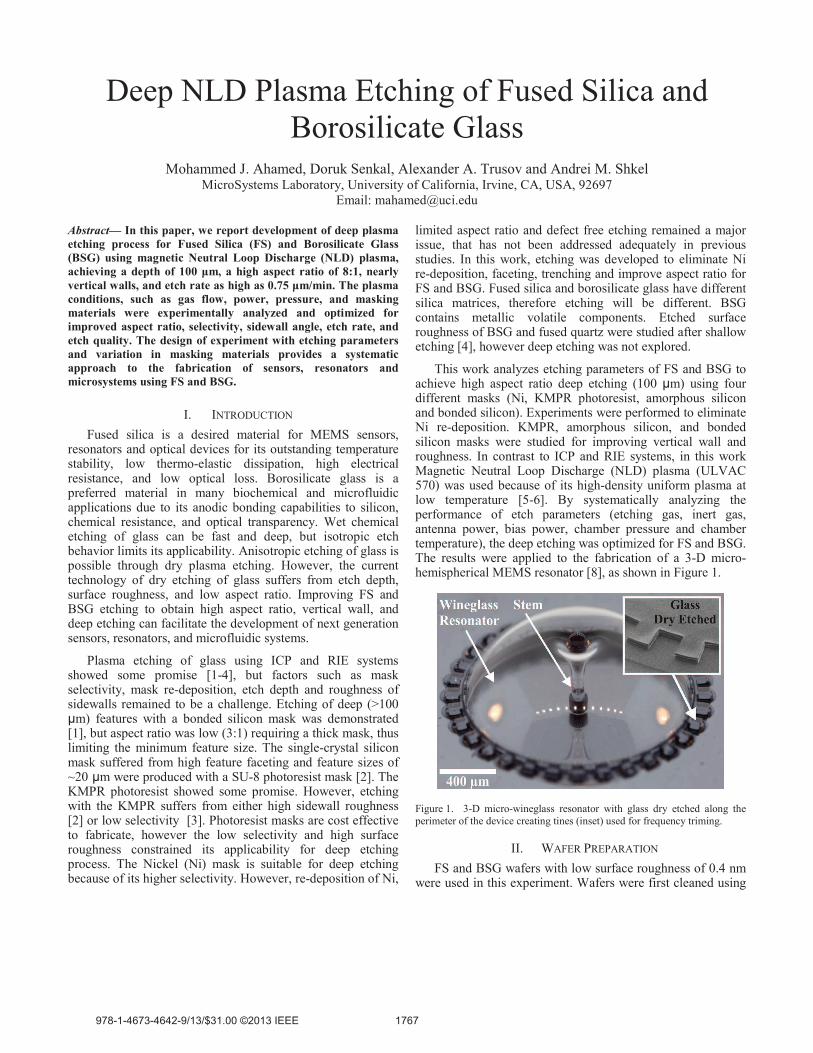
This work analyzes etching parameters of FS and BSG to achieve high aspect ratio deep etching (100 µm) using four different masks (Ni, KMPR photoresist, amorphous silicon and bonded silicon). Experiments were performed to eliminate Ni re-deposition. KMPR, amorphous silicon, and bonded silicon masks were studied for improving vertical wall and roughness. In contrast to ICP and RIE systems, in this work Magnetic Neutral Loop Discharge (NLD) plasma (ULVAC 570) was used because of its high-density uniform plasma at low temperature [5-6]. By systematically analyzing the performance of etch parameters (etching gas, inert gas, antenna power, bias power, chamber pressure and chamber temperature), the deep etching was optimized for FS and BSG. The results were applied to the fabrication of a 3-D micro-hemispherical MEMS resonator [8], as shown in Figure 1.
Figure 1. 3-D micro-wineglass resonator with glass dry etched along the
perimeter of the device creating tines (inset) used for frequency triming.
II. WAFER PREPARATION
FS and BSG wafers with low surface roughness of 0.4 nm were used in this experiment. Wafers were first cleaned using
1767
solvent and RCA-1, followed by DI water rinse. The glass etching was performed on a ULVAC 570 glass etcher. In our design of experiments, we varied a number of process parameters, including etching gas C3F8 10-40 sccm, neutral gas Argon (Ar) 0-200 sccm, bias power 50-200 W, antenna power 800-1600 W, and chamber pressure 5-15 mT. Four different etch masks (metal, bonded silicon, KMPR, and amorphous silicon) were compared. Plasma conditions (gas flows, plasma power, and chamber pressure) were investigated to optimize etching performance by analyzing aspect ratio, mask selectivity, wall angle, etch rate, surface roughness, and feature quality of FS and BSG.
III. VARIATION OF ETCH MASK
Four different etch mask were tested and results are
summarized in Table 1.
TABLE I. COMPARATIVE ANALYSIS OF DIFFERENT ETCH MASK
A. Electroplated Nickel
As indicated in Table-1, for deeper etching, a Ni metal mask is favorable because of its 70:1 selectivity. A low-stress 5 µm thick electroplated Nickel (Ni) metal mask was used to resolve a minimum feature size of 5 µm. It was then optimized for low stress by testing thermal treatment of up to 400
0C, measuring wafer bowing and delaminating. The
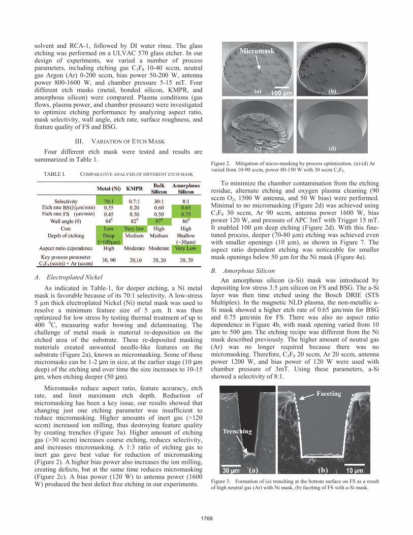
challenge of metal mask is material re-deposition on the etched area of the substrate. These re-deposited masking materials created unwanted needle-like features on the substrate (Figure 2a), known as micromasking. Some of these micromasks can be 1-2 µm in size, at the earlier stage (10 µm deep) of the etching and over time the size increases to 10-15 µm, when etching deeper (50 µm).
Micromasks reduce aspect ratio, feature accuracy, etch rate, and limit maximum etch depth. Reduction of micromasking has been a key issue, our results showed that changing just one etching parameter was insufficient to reduce micromasking. Higher amounts of inert gas (>120 sccm) increased ion milling, thus destroying feature quality by creating trenches (Figure 3a). Higher amount of etching gas (>30 sccm) increases coarse etching, reduces selectivity, and increases micromasking. A 1:3 ratio of etching gas to inert gas gave best value for reduction of micromasking (Figure 2). A higher bias power also increases the ion milling, creating defects, but at the same time reduces micromasking (Figure 2c). A bias power (120 W) to antenna power (1600 W) produced the best defect free etching in our experiments.
Figure 2. Mitigation of micro-masking by process optimization. (a)-(d) Ar
varied from 10-90 sccm, power 80-150 W with 30 sccm C3F8.
To minimize the chamber contamination from the etching residue, alternate etching and oxygen plasma cleaning (90 sccm O2, 1500 W antenna, and 50 W bias) were performed. Minimal to no micromasking (Figure 2d) was achieved using C3F8 30 sccm, Ar 90 sccm, antenna power 1600 W, bias power 120 W, and pressure of APC 3mT with Trigger 15 mT. It enabled 100 µm deep etching (Figure 2d). With this fine-tuned process, deeper (70-80 µm) etching was achieved even with smaller openings (10 µm), as shown in Figure 7. The aspect ratio dependent etching was noticeable for smaller mask openings below 50 µm for the Ni mask (Figure 4a).
B. Amorphous Silicon
An amorphous silicon (a-Si) mask was introduced by depositing low stress 3.5 µm silicon on FS and BSG. The a-Si layer was then time etched using the Bosch DRIE (STS Multiplex). In the magnetic NLD plasma, the non-metallic a-Si mask showed a higher etch rate of 0.65 µm/min for BSG and 0.75 µm/min for FS. There was also no aspect ratio dependence in Figure 4b, with mask opening varied from 10 µm to 500 µm. The etching recipe was different from the Ni mask described previously. The higher amount of neutral gas (Ar) was no longer required because there was no micromasking. Therefore, C3F8 20 sccm, Ar 20 sccm, antenna power 1200 W, and bias power of 120 W were used with chamber pressure of 3mT. Using these parameters, a-Si showed a selectivity of 8:1.
Figure 3. Formation of (a) trenching at the bottom surface on FS as a result
of high neutral gas (Ar) with Ni mask, (b) faceting of FS with a-Si mask.
1768

Figure 4. Aspenct ratio dependent etching, shown in top figure (a), was
mitigated as shown in bottom figure (b), by using a process receipe of C3F8
20 sccm, Ar 20 sccm, antenna 1200 W, bias 120 W, and a-Si etch mask.
Faceting was noticed with the a-Si and the bonded-Si masks (Figure 3b). Due to the lower selectivity (8:1), a-Si was not favorable for deeper etching. The maximum possible amount of a-Si deposition is limited by the deposition process. Therefore, a-Si is suitable for shallow etching, and especially applicable for microfluidic channels due to low etch roughness and nearly vertical wall. The other advantages of a-Si mask over other masks are aspect ratio independence (Figure 4b).
C. KMPR Photoresist
The KMPR photoresist (Microchem) mask was processed using standard lithography technique. KMPR was selected in this NLD plasma study because it is non-metallic, simple to fabricate, and capable of producing vertical walls. However, our results show its low selectivity <1 (Table 1). The other disadvantage noticed was the deposition of large amount of consumed KMPR on the chamber, wall, and substrate. For the KMPR mask, a higher amount of Ar cannot be used because it decreases selectivity. Alternating of etching (C3F8 of 20 sccm, Ar 10 sccm, antenna power 1200 W, and bias 80 W) and O2 plasma cleaning were necessary to reduce contamination. The low <1 selectivity and high contamination made it unfavorable for deeper etching.
D. Bonded Silicon
A bonded silicon mask was achieved by using plasma assisted fusion bonding between silicon to FS and silicon to BSG. Seamless high strength plasma bonding, that was earlier reported by the authors [7] was used for the bonding. The bonded silicon layer was patterned using the Bosch DRIE (STS Multiplex) process. The glass etching recipe was similar to a-Si described above, but the etching performance showed the aspect ratio dependence. It showed higher selectivity 30:1. However, as a result of high mask thickness, deep etching was not possible for smaller mask opening (<30 µm) due to difficulty in accessing small openings with plasma. Increase in Ar (>50 sccm) and power (>1200 W) helps, however it distorts features because of high ion bombardment. The other challenges are cost and fabrication complexity associated with wafer bonding and the thin silicon
layer. The CTE mismatch between bonded silicon and the glass layer resulted in occasional wafer bow, limiting its use for longer etching.
IV. ETCHING OF FS AND BSG
Etching performance of FS and BSG was compared with the ultimate goal to achieve deep etching. BSG etches faster for the first 20-30 µm of deep etching because of the release of volatile impurities. For deeper etching ~100 µm, the overall etch rate of FS was higher compared to BSG with the masking materials tested in this work. Nearly vertical wall etching was possible on FS (87
0), as shown in Figure 5.
Figure 5. Deep etching on FS with vertical wall angle of 870 and deep
etching of BSG with vertical wall angle of 840. Deep etching of 100 µm with
no faceting or trenching was achieved (right).
Roughness of etched surfaces (bottom and vertical wall) were measured for both FS and BSG using an atomic force microscope (AFM) from Pacific Nanotechnology (Nano-R). After etching of 10 µm deep, BSG showed sharper peaks compared to FS (Figure 6). The presence of volatile impurities and difference in densities of SiO2 matrix are associated with the relatively rough surface on BSG. Plasma etching inside the chamber occurs through simultaneous chemical and ion milling. Surface roughness can be minimized by balancing between the chemical and physical etching. When there is no neutral gas (e.g., Ar), the etching is governed by chemical gas that creates a rough surface and the roughness keep increasing over time.
Figure 6. AFM surface morpholgies of FS and BSG after 10 µm deep
etching showing BSG surface roughness has sharper peaks due to release of
impurities from SiO2 matrix as compared to FS.
1769
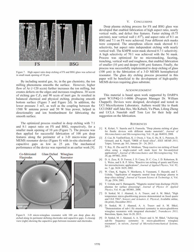
Figure 7. High aspect ratio deep etching of FS and BSG glass was achieved
in small mask opening of 10 µm.
By including neutral gas, Ar, in the gas chemistry, the ion milling phenomena smooths the surface. However, higher flow of Ar (>120 sccm) further increases the ion milling, but creates defects on the edges and increases roughness. 30 sccm of etching gas C3F8 and 90 sccm of inert gas Ar resulted in balanced chemical and physical etching, producing smooth bottom surface (Figure 5 and Figure 2d). In addition, the lower pressure 3 mT, as well as the coupling between the 1500 W antenna power and 50 W bias power, helped in directionality and ion bombardment for fabricating the smooth surface.
The optimized process resulted in deep etching with 7:1
and 8:1 aspect ratio on FS and BSG, respectively, for a smaller mask opening of 10 µm (Figure 7). The process was then applied for successful fabrication of 100 µm deep features along the perimeter of a 3-D micro-wine glass MEMS resonator device (Figure 8) with in-situ electrodes of capacitive gaps as low as 25 µm. The mechanical performance of the device was reported in an earlier work [9].
Figure 8. 3-D micro-wineglass resonator with 100 µm deep glass dry
etched along its perimeter defining electrodes and capacitive gaps. A closeup
view (right) showing the capacitive gaps between resonator and electrodes.
V. CONCLUSIONS
Deep plasma etching process for FS and BSG glass was developed that enabled fabrication of high aspect ratio, nearly vertical walls, and defect free features. Faster etching (0.75 µm/min), near vertical wall (~87
0), and aspect ratio of 8:1 on
BSG and 7:1 on FS were achieved. Four different etch masks were compared. The amorphous silicon mask showed 8:1 selectivity, but aspect ratio independent etching with nearly vertical wall. The KMPR resist mask showed 0.7:1 selectivity. A high selectivity of 70:1 was achieved with the Ni mask. Process was optimized for no micromasking, faceting, trenching, vertical wall and roughness, that enabled fabrication of smaller (10 µm) and deeper (100 µm) features. Finally, the process was successfully implemented to deep etching of glass (100 µm) in the fabrication of a 3-D MEMS hemispherical resonator. The glass dry etching process presented in this paper will be beneficial to the development of high-quality MEMS devices requiring glass substrate.
ACKNOWLEDGMENT
This material is based upon work supported by DARPA grant W31P4Q-11-1-0006 (Program Manager Dr. William Chappell). Devices were designed, developed and tested in UCI MicroSystems Laboratory. Authors would like to thank UCI INRF staff Jake Hes, Mo Kebaili, Vu Phan, Lifeng Zheng and UCLA Nanolab staff Tom Lee for their help and suggestion on the fabrication.
REFERENCES
[1] K. Kolari, V. Saarela and S. Franssila, "Deep plasma etching of glass for fluidic devices with different masks materials", Journal of Micromechanics and Microengineering, Vol. 18, pp. 064010, 2008.
[2] Z. Cao, B. VanDerElzen, K. J. Owen, J. Yan, G. He, R. L. Peterson, D. Grimard, and K. Najafi, "DRIE of fused silica", IEEE MEMS 2013, Taipei, Taiwan, pp. 361, January 20 – 24, 2013.
[3] T. Ray, H. Zhu and D. R. Meldrum, "Deep reactive ion etching of fused silica using a single-coated soft mask layer for bio-analytical applications", Journal of Micromechanics and Microengineering. Vol. 20, pp. 097002, 2010.
[4] D. A. Zeze, R. D. Forrest, J. D. Carey, D. C. Cox, I. D. Robertson, B. L. Weiss, and S. R. P. Silva, "Reactive ion etching of quartz and Pyrex for microelectronic applications", Journal of Applied Physics, Vol. 92, no. 7, pp. 3624–3629, 2002.
[5] W. Chen, K. Sugita, Y. Morikawa, S. Yasunami, T. Hayashi, and T. Uchida, "Application of magnetic neutral loop discharge plasma in deep silica etching", Journal of Vacuum Science & Technology A, Vol. 19, pp. 2936, 2001.
[6] T. Uchida and S. Hamaguchi, "Magnetic neutral loop discharge (NLD) plasmas for surface processing", Journal of Physics D: Applied Physics, Vol. 41, pp. 083001, 2008.
[7] D. Senkal, M. J. Ahamed, A. A. Trusov, and A. M. Shkel, "High temperature micro-glassblowing process demonstrated on fused quartz and ULE TSG", Sensors and Actuators A: Physical, Available online, (In print), December 2012.
[8] D. Senkal, M. J. Ahamed, A. A. Trusov and A. M. Shkel, "Demonstration of sub-1 Hz structural symmetry in micro-glassblown wineglass resonators with integrated electrodes", Transducers 2013, Barcelona, Spain, June 16-20, 2013.
[9] D. Senkal, M. J. Ahamed, A. A. Trusov and A. M. Shkel, "Achieving sub-Hz frequency symmetry in micro-glassblown wineglass resonators", in reivew, Journal of Microelectromechanical Systems, 2013.
1770