defect levels in the amorphous selenium...
TRANSCRIPT
Katholieke Universiteit LeuvenFaculteit der WetenschappenDepartement Natuurkunde en SterrenkundeLaboratorium voor Halfgeleiderfysica
Defect Levels in the Amorphous
Selenium Bandgap
Mohammed Loutfi Benkhedir
Promotor:Prof. Dr. G.J. Adriaenssens
Proefschrift ingediend tothet behalen van de graad vanDoctor in de Wetenschappen
2006
D/2006/10.705/24ISBN 90-8649-027-1

iii
Dedication
To my mother and to the memory of my fatherto my daughters
and to my wife Nadia
iv
Acknowledgement
Who does not thank people does not thank god. I owe a lot of thanks to allthose who have contributed to the production of this work.
Special thanks go to my promoter Guy J. Adriaenssens for accepting tosupervise my work, for his constant guidance throughout my PhD journeyas well as his fruitful discussions and insightful comments.
I express a lot of gratitude for the jury members for having taken time toread and comment on my thesis. Special thanks go to Andre Stesmans andChrist Glorieux for accepting to be my PhD committee members.
I am also grateful to Prof. S. O. Kasap for providing me with somesamples and for constructive discussions.
I would like to thank Prof. J. M. Marshall and Dr. Zhenia Emelianova forthe simulations they did on my experimental results as well as for the fruitfuldiscussions. My thanks go also to J. Willekens for doing CPM measurementsas well as to M. Brinza for helping me to use the TOF setup.
This work would not have been possible without the warm atmosphereand the nice moments during coffee times with all the members of the HFgroup. Thank you for you all.
I also express my gratitude to the BTC for the financial support of myPhD programme. Special thanks go to S. Vanloo, C. Misigaro and C. Leroy.
My thesis would not have been possible without the friendly atmosphereprovided by all the Arab friends. Thank you for you all for the nice mo-ments we enjoyed together. Your friendship and company helped me a lot toaccomplish this work.
v
vi
Contents
List of Abbreviations 1
Samenvatting 3
Introduction 7
1 Amorphous chalcogenides 11
1.1 Energy bands in amorphous semiconductors . . . . . . . . . . 11
1.1.1 The solution in the crystalline case . . . . . . . . . . . 12
1.1.2 Amorphous materials . . . . . . . . . . . . . . . . . . . 13
1.1.3 Electron localization . . . . . . . . . . . . . . . . . . . 17
1.2 Bonding in amorphous semiconductors . . . . . . . . . . . . . 17
1.2.1 Bonding defects in amorphous semiconductors . . . . . 19
1.2.2 Behavior of the Fermi level . . . . . . . . . . . . . . . . 27
1.3 Selenium . . . . . . . . . . . . . . . . . . . . . . . . . . . . . . 28
1.3.1 Microstructure of selenium . . . . . . . . . . . . . . . . 28
1.3.2 Optical properties of a-Se . . . . . . . . . . . . . . . . 30
1.3.3 Electronic properties . . . . . . . . . . . . . . . . . . . 32
2 Photoconductivity techniques 35
2.1 General concepts . . . . . . . . . . . . . . . . . . . . . . . . . 35
2.2 Steady-state photoconductivity . . . . . . . . . . . . . . . . . 40
2.2.1 Effect of light intensity . . . . . . . . . . . . . . . . . . 41
2.2.2 Effect of temperature . . . . . . . . . . . . . . . . . . . 42
2.3 Optical absorption coefficient . . . . . . . . . . . . . . . . . . 45
2.4 Transient photocurrent techniques . . . . . . . . . . . . . . . . 46
2.4.1 Time-of-flight technique . . . . . . . . . . . . . . . . . 46
2.4.2 Transient photocurrent . . . . . . . . . . . . . . . . . . 50
2.4.3 Multiple-trapping transport model . . . . . . . . . . . 51
vii
viii CONTENTS
3 Thermal transitions in the negative-U energy scheme for a-Se 573.1 Steady-state photoconductivity . . . . . . . . . . . . . . . . . 57
3.1.1 Experimental results . . . . . . . . . . . . . . . . . . . 573.1.2 Discussion . . . . . . . . . . . . . . . . . . . . . . . . . 61
3.2 Post-transit photocurrent analysis (PTPA) . . . . . . . . . . . 643.2.1 Experimental results . . . . . . . . . . . . . . . . . . . 663.2.2 Discussion . . . . . . . . . . . . . . . . . . . . . . . . . 68
3.3 Transient photocurrent decay . . . . . . . . . . . . . . . . . . 733.3.1 Experimental results . . . . . . . . . . . . . . . . . . . 733.3.2 Discussion . . . . . . . . . . . . . . . . . . . . . . . . . 75
3.4 Concluding discussion . . . . . . . . . . . . . . . . . . . . . . 75
4 Optical transitions in negative-U model 774.1 Experimental conditions . . . . . . . . . . . . . . . . . . . . . 78
4.1.1 Samples . . . . . . . . . . . . . . . . . . . . . . . . . . 784.1.2 Experimental set-ups . . . . . . . . . . . . . . . . . . . 78
4.2 Experimental results . . . . . . . . . . . . . . . . . . . . . . . 804.3 Discussion . . . . . . . . . . . . . . . . . . . . . . . . . . . . . 834.4 Conclusion . . . . . . . . . . . . . . . . . . . . . . . . . . . . . 86
5 Defects not related to the negative-U system 875.1 Experimental considerations . . . . . . . . . . . . . . . . . . . 875.2 Experimental results . . . . . . . . . . . . . . . . . . . . . . . 88
5.2.1 Deep levels . . . . . . . . . . . . . . . . . . . . . . . . 885.2.2 Shallow levels . . . . . . . . . . . . . . . . . . . . . . . 90
5.3 Discussion . . . . . . . . . . . . . . . . . . . . . . . . . . . . . 955.3.1 Deep levels . . . . . . . . . . . . . . . . . . . . . . . . 955.3.2 Shallow levels . . . . . . . . . . . . . . . . . . . . . . . 97
5.4 Conclusion . . . . . . . . . . . . . . . . . . . . . . . . . . . . . 100
6 Tail-state distributions in a-Se 1036.1 Experimental results . . . . . . . . . . . . . . . . . . . . . . . 103
6.1.1 Transient photocurrent method . . . . . . . . . . . . . 1036.1.2 Drift mobility method . . . . . . . . . . . . . . . . . . 105
6.2 Discussion . . . . . . . . . . . . . . . . . . . . . . . . . . . . . 1076.3 Conclusion . . . . . . . . . . . . . . . . . . . . . . . . . . . . . 109
7 Photoinduced changes in a-Se 1117.1 Experimental results . . . . . . . . . . . . . . . . . . . . . . . 112
7.1.1 Excessively used TOF samples . . . . . . . . . . . . . . 112
CONTENTS ix
7.1.2 Samples illuminated with natural light . . . . . . . . . 1147.1.3 Halogen lamp illumination . . . . . . . . . . . . . . . . 1147.1.4 Annealing effect . . . . . . . . . . . . . . . . . . . . . . 116
7.2 Discussion . . . . . . . . . . . . . . . . . . . . . . . . . . . . . 1167.3 Conclusion . . . . . . . . . . . . . . . . . . . . . . . . . . . . . 119
Summary and conclusions 121
Bibliography 125
Publication List 133

x CONTENTS
List of Abbreviations
a-Se Amorphous seleniumCB Conduction bandCPM Constant photocurrent methodCRN Continuous random networkDC Direct currentDOS Density of statesESR Electron spin resonanceKAF Kastner, Adler and FritzscheLESR Light-induced electron spin resonancePDS Photothermal deflection spectroscopyPTPA Post-transit photocurrent analysisSSPC Steady-state photoconductivityTOF Time-of-flightTPC Transient photoconductivityTROK Tiedje and Rose and Orenstein and KastnerVB Valence band
1
2 List of Abbreviations
Samenvatting
De elektronische toestandsdichtheid in de bandkloof van amorf seleen (a-Se) is het onderwerp van deze thesis. Ondanks de lange voorgeschiedenisvan amorf seleen als de eerste fotogeleidende halfgeleider, die onder meerwerd gebruikt in fotocopieerapparaten en als elektronische schakelaar, zijneen aantal van zijn eigenschappen nog steeds twijfelachtig en zelfs onbek-end gebleven. Een kenschetsend voorbeeld van deze toestand is het feit dat,hoewel een zeer specifiek, op seleen gebaseerd model voor coordinatiedefectenmet effectieve negatieve elektroncorrelatie-energie (negatieve-U) als tekst-boekvoorbeeld wordt gebruikt voor dergelijke defecten in het amorfe rooster,sommige onderzoekers er nog aan twijfelen of de toestandsdichtheid van hetamorfe seleen zelf wel dergelijke roosterdefecten omvat.
Het gangbare model voor de toestandsdichtheid van a-Se werd in 1988door Abkowitz voorgesteld. Naast steile bandstaarten aan beide zijden vande bandkloof bevat het model twee ondiepe defectniveaus, zowat 0.3 eV ver-wijderd van de bandkanten, en twee diepe vangstcentra ongeveer in het mid-den van de 1.95 eV brede bandkloof en symmetrisch ten opzichte van hetFermi-niveau. Verschillende elementen van dit model moeten evenwel invraag worden gesteld. De activeringsenergie van de driftmobiliteit van zowelgaten als elektronen werd ten onrechte gebruikt als energieafstand van deondiepe niveaus tot de bandkanten, en van de diepe toestanden werd veron-dersteld dat ze met thermische overgangen overeenkomen in het negatieve-Umodel hoewel dat model zelf hogere energieen veronderstelt. Een nieuwe,gedetailleerde studie van de a-Se toestandsdichtheid is bijgevolg aangewezen.
Om die toestandsdichtheid van het a-Se te onderzoeken wordt in dezethesis vooral gebruik gemaakt van een aantal stationaire en transiente fo-togeleidingstechnieken. Er wordt aangetoond dat a-Se wel degelijk tot degroep van de negatieve-U materialen mag worden gerekend. Het energie-schema voor verschillende ofwel thermisch ofwel optisch geınduceerde elek-tronische transities die gepaard gaan met het geheel van elektrisch geladen,negatieve-U defecten kon worden afgeleid.
Voor de thermische overgangen naar het negatief geladen defect D− wordtop basis van post-transit analyse van de ’time-of-flight’ (TOF) transientefotostroom een niveau gelocaliseerd ∼ 0.4 eV boven de valentieband, EV ,terwijl de temperatuursafhankelijkheid van de stationaire fotostroom tot eenwaarde van ∼ 0.36 eV boven EV leidt. Het verschil laat zich verklaren dooreen waargenomen sensitisatie van de stationaire fotostroom bij lage temper-aturen. Voor de thermische overgangen naar het positief geladen D+ wordt
3
4 Samenvatting
anderzijds een niveau ∼ 0.53 eV onder de conductiebandkant, EC , gevon-den op basis van zowel de TOF post-transit analyse als van de stationairefotostroommetingen.
De optische absorptie door bemiddeling van de negatieve-U centra werdbestudeerd aan de hand van de constante-fotostroom-methode en van foto-thermische deflectiespectroscopie. Het aan D+ verbonden absorptieniveauligt ∼ 1.5 eV boven EV , en absorptie vanuit D− naar EC vraagt ∼ 1.75 eV.Deze waarden plaatsen de optische transitieniveaus net voorbij de thermi-sche niveaus naar de bandkanten toe, en suggereren dat het potentiaalprofielvan de D+ en D− defecten slechts een kleine kromming vertoont in configu-ratieruimte. Het geheel van de gevonden thermische en optische transitie-energieen sluit goed aan bij het algemeen concept van de negatieve-U de-fecten, maar is duidelijk in tegenspraak met het hoger geciteerde Abkowitzmodel.
Naast de negatieve-U defecten bevat de a-Se toestandsdichtheid evenwelook nog neutrale defecten dicht bij de bandkanten, en diepe defecten in debuurt van de het Fermi-niveau. Waar een knik in het pre-transit elektronTOF-signaal op de aanwezigheid wijst van een discreet defectniveau 0.3 eVbeneden EC , duidt een analoge knik in de transiente fotostroom gemeten ineen co-planaire elektrodegeometrie, op een corresponderend niveau 0.2 eVboven EV . Dat beide ondiepe centra elektrisch neutraal zijn blijkt uit hunlage waarden voor de ontsnappingsfrequentie: eerder 1010 Hz dan de 1012 Hzvan de geladen D+ en D− defecten. Een moleculaire configuratie waarbij deniet-bindende p-orbitalen van twee Se buren parallel met elkaar eerder danloodrecht ten opzichte van elkaar georienteerd zijn kan als oorsprong van diedefecten worden aangewezen. Voor de defecttoestanden diep in de bandkloofis het niet mogelijk hun positie precies te bepalen. Hun aanwezigheid, alszowel elektronen- als gatenvangstcentrum, wordt afgeleid uit het verlies vande signaalamplitude bij repetitieve TOF metingen omwille van recombinatiemet lading in de diepe vangstcentra. Het diepe elektron-vangstcentrum leidttevens tot sensitisatie van de stationaire fotostroom bij lage temperaturen.
Tenslotte werd ook aandacht besteed aan de bandstaarten van het a-Se.Een analyse van de gatenmobiliteit in functie van temperatuur en aangelegdelektrisch veld laat toe een exponentiele toestandsverdeling met een karak-teristieke energie van 25 meV voor te stellen als achtergrondsdichtheid aande valentiebandkant van de bandkloof. Modelberekeningen voor de TOFstroomtransienten ondersteunen die analyse. Omwille van de veldonafhanke-lijkheid van de elektronenmobiliteit zijn voor de conductiebandkant van dekloof enkel modelberekingen beschikbaar. Ze wijzen op een exponentieleverdeling met 20 meV als karakteristieke energie.
Samenvattend mag worden gesteld dat deze thesis het heuristische Abko-
Samenvatting 5
witz model heeft kunnen vervangen door een omstandig gedocumenteerdmodel dat zowel de geladen coordinatiedefecten van het negatieve-U sys-teem omvat als ondiepe neutrale toestanden veroorzaakt door afwijkendeorbitaalorientaties, en diepe vangstcentra van nog ongewisse oorsprong.

6 Samenvatting

Introduction
Selenium (Se), one of the chalcogen elements (sulphur, selenium and tel-lurium), has been the first photoconductor discovered in 1873 [1]. W. Smithwas using rods of Se as resistors to test sub-marine telegraphic cables whenhe discovered that its resistance depends on whether the resistor is illumi-nated or not. The selenium solar cell was reported in 1883 by Charles Fritts,and it was available in the market from the 1920s until the 1950s when sili-con solar cells were produced. The crystalline form of selenium was used inelectrical rectifiers from the 1930s to the 1960s; after this it was replaced bysilicon devices. However, its more important application was in xerography[2]; this application continued until the late 1980s when organic semicon-ductors emerged. The photoconductivity of Se, in its amorphous form, isstill attractive. Today, two imaging applications are using it: The first isits use as an avalanche photoconductor in ultrahigh sensitivity vidicon tubes(HARPICONs) [3]; the second is its use as an X-ray photoconductor in directconversion X-ray detectors [4].
These last two applications stimulated the research work on amorphousselenium (a-Se), especially on its electronic properties. It is surprising that,despite this long history of Se usage our knowledge about it is really notsufficient to understand many of its properties. Se has two main crystallineforms, trigonal γ-Se constructed of infinite helical chains and monoclinic Seconsisting of 8-fold Se rings. In the trigonal Se, holes are the more mobilecarriers [5], while electron mobility is higher in the monoclinic crystal [6]. Itis accepted that a-Se is constructed of random chains, in such a way thatall atoms are two-fold coordinated in chains with a constant dihedral angle,but this angle is changing its sign randomly [7]. This makes a-Se a mixtureof chain and ring fragments that allows both electrons and holes to attainmeasurable drift mobilities.
In 1988 Abkowitz [8] proposed a model for the electronic density of statesin the a-Se band gap. This model consists of steep tail-state distributionsin both sides of the gap, two features at about 0.3 eV from the band edges,and two deep defect bands near the mid-gap Fermi level. While the 0.3eV features were erroneously deduced from drift mobility measurements ofholes and electrons in function of temperature and field [9], the two mid-gap levels were deduced from xerographic residual potential data that aredifficult to interpret. This makes the Abkowitz model doubtful and justifiesa re-examination of the density of states (DOS) distribution in the gap ofa-Se.
7
8 Introduction
Another reason for investigating the a-Se DOS lies with the fact that se-lenium is used routinely as an example to illustrate the concept of negativeeffective electron correlation energy (negative-U concept) in chalcogenides[10]. However, in spite of the existence of a detailed model for the negative-U defects in a-Se [11], doubts were raised concerning the actual negative-Ucharacter of the material [12] [13]. Recently Kolobov [14] presented exper-imental proof, based on light-induced electronic spin resonance (LESR) forthe presence of the negative-U defects in a-Se. However, this still leaves theposition of the defect energy levels in the band gap unresolved. It is still rel-evant therefore, to probe this with other simple techniques like steady-statephotoconductivity (SSPC). The negative-U centers are characterized by astrong electron-phonon coupling that leads to different transition energiesfor thermal and optical excitations. Consequently one needs several experi-mental techniques to track the different possible transitions in a negative-Usystem scheme. The thermally accessible levels can be seen using the time-of-flight (TOF) technique and SSPC. The optically accessible ones can beseen using the constant photocurrent method (CPM), spectral photocurrentdistribution, and photo-thermal deflection spectroscopy (PDS).
Theoretical considerations predict that in negative-U systems the ener-getic positions of the concerned defects are situated roughly one quarter ofthe forbidden gap from the bands edges. For a-Se the energy gap is around 2eV, then two defect levels will be somewhere around 0.5 eV from the edges.However the presence of these negative-U centers does not preclude the ex-istence of other non-related defects in the a-Se lattice.
The glass transition temperature of selenium is just above room temper-ature, around 42 C, which makes a-Se rather unstable and in danger ofunintended crystallization. To avert this problem in technological applica-tions, a trace of As, in the order 0.5 at% , is added to stabilize the a-Sematrix. The glass transition temperature of stabilized selenium is about 70C. This thesis contains a study of the electronic properties of pure and sta-bilized a-Se, thin films or bulk, using the above techniques in order to dealwith the previously cited problems. This thesis is divided in 7 chapters asfollows:
In Chapter 1 a brief review of some relevant topics concerning the physicsof amorphous semiconductors is given. These topics include the band struc-ture in amorphous semiconductors, and some new terms in comparison withcrystalline materials, like mobility edge and localization. Subsequently, thespecific case of chalcogenide semiconductors will be discussed. These arecompounds where one (or more) of the chalcogens are an essential compo-nent. The emphasis will be on amorphous selenium and its properties, as itis the subject of this thesis.

Introduction 9
In Chapter 2 the photoconductivity in semiconductors will be introducedas an experimental tool to probe the electronic properties of the material.Indeed, the extra free charge carriers created by the photon absorption willcontribute to the electronic transport under an applied electric field. Theywill interact with material defects, and at the end these extra charge carriersare injected in the external circuit or just recombine in different ways. Twodifferent regimes can be discussed in the photocurrent. First there is thetransient one and secondly the steady state. In both cases the photocurrentforms the basis of several experimental techniques, some of which will beused in this study of a-Se.
In Chapter 3 the focus will be on the T+ and T− levels related to thenegative-U model in a-Se using transient TOF , TPC and SSPC techniques.The detection of the T+ and T− levels will be a first step to answer thequestion wether a-Se is a negative-U system or not.
Chapter 4 will focus on the optical transitions involved in the negative-U model. the energetic position of the corresponding levels will be furtherevidence that, as other chalcogenides, a-Se is a negative-U system.
In Chapter 5 evidence for the existence of deep levels around the Fermilevel, and shallow defects in the neighborhood of the band-edges will be given.These defects are not related to the charged ones involved in the negative-Umodel. The shallow ones are traced to a specific defect in the dihedral anglethat puts lone pairs in a-Se parallel rather than perpendicular.
In Chapter 6 the tail-state distribution at both sides of the bandgap willbe discussed. Experimentally, for the valence band side the variation of holemobility in function of temperature and applied field and TPC will be used toprobe the steepness of tail-state distribution. For conduction band side theonly alternative for the study of the tail-state distribution are calculations.
Finally Chapter 7 presents the effect of light soaking on the DOS ofa-Se. It contains the surprising observation of a photo-induced change ina-Se that is stable at room temperature, in spite of the low glass transitiontemperature.

10 Introduction

Chapter 1
Amorphous chalcogenides
This chapter gives a brief review of some relevant topics concerning thephysics of amorphous semiconductors. These topics include the band struc-ture in amorphous semiconductors, and some new terms in comparison withcrystalline materials, like mobility edge and localization. Subsequently, thespecific case of chalcogenide semiconductors will be discussed. These arecompounds where one (or more) of the chalcogens are an essential compo-nent. The emphasis will be on amorphous selenium and its properties, asit is the subject of this thesis. More detailed information is available in thetextbooks by Elliott [10] and Mott and Davis [15].
1.1 Energy bands in amorphous semiconduc-
tors
Crystalline materials consist of an arrangement of a structural unit (oneor more atoms) in a three-dimensional ordered network. Using quantummechanics theory, physicists are able to analyse electronic properties of crys-talline semiconductors with their high degree of symmetry. The long-rangeorder not only simplifies considerably mathematical calculation of the crys-tal system, but it forms the base to solve the Shrodinger equation for anelectron in a crystal. Amorphous materials in the other hand do not exhibitthis long-range order, and the existence of such materials with comparablecharacteristics to the crystalline ones stimulated physicists to reexamine therole of long-range order in defining the electronic properties of solids. Thekey point is that amorphous materials do not lose every sense of order. Itwas demonstrated that at short range crystalline and amorphous materialshave comparable structures.
11
12 Chapter 1. Chalcogenides
1.1.1 The solution in the crystalline case
In an isolated atom, quantum mechanics predicts that electrons can lie only indiscrete possible states with discrete energy. The distribution of the electronsof this atom over these possible states obeys Pauli′s exclusion principle, thatone electronic state can support only two electrons, one with spin up andthe other with spin down. This fact is the origin of the properties of anyelement. In this thesis we are dealing with elements that have eight possiblestates (spin taken into account) in the outermost shell. According to thenumber and distribution of electrons at each atom, these atoms can bond(as will be shown briefly below) to form a molecule or a solid. At this stageatomic or molecular orbitals spread to form bands of energy, where electronscan lie in a solid. The last fully occupied band is called valence band and thefirst allowed but unoccupied band is called the conduction band. If there isan energy gap (forbidden gap) between the top of the valence band and thebottom of the conduction band that is small (generally less than 2.5 eV), andif the Fermi level is situated in this forbidden gap the material in question isa semiconductor.
What we saw in the last paragraph is a phenomenological description ofthe energetic distribution of electrons in a solid. To find a mathematical de-scription we use several approximations to reduce the problem from a many-electron one to a single-electron problem. This is possible by taking intoaccount the electron-electron interaction in a chosen effective one-electronpotential U (r). We can write the Shrodinger equation for an electron in acrystalline solid as follows:
HΨ = (− h2
2m∇2 + U(r))Ψ = EΨ, (1.1)
where H is the Hamiltonian, m the electron mass, E the energy eigenvalueand Ψ is the wave function.
According to Bloch′s theorem the wave function of an electron in theperiodic potential of a crystal is a plane wave times a function with the sameperiodicity as the crystal lattice:
Ψnk(r) = eik.ru
nk(r). (1.2)
The vector k is a quantum vector defined in the reciprocal space while r ischaracteristic of the periodic potential of the lattice. For a Given vector kthere are many solutions to the Shrodinger equation, with discretely spacedeigenvalues, as indicated by the index n in the above equation. The energylevels of an electron in the solid crystal are thus described by the functions
1.1. Energy bands 13
En(k). These functions are continuous in reciprocal space, with each valueof n defining a band of allowed electron energies in the crystal. Collectivelythey are referred to as the electronic band structure of the crystal.
1.1.2 Amorphous materials
In amorphous materials the band structure problem is more complicated bythe lack of long-range order. The word amorphous suggests that there isno order in the network, but in reality it turns out that the short-range or-der in amorphous materials is practically the same as in the correspondingcrystalline materials. Using this short-range order it is possible to demon-strate that amorphous materials do have a band structure, the absence oflong-range order notwithstanding.
Microstructure in amorphous materials
To describe the short-range order we use the radial distribution function(RDF) which derives its significance from the fact that it is obtained directlyfrom diffraction experiments. This function, symbolized as J(r), is defined asthe number of atoms lying at distances between r and r+dr from the centerof an arbitrary origin atom. It can be written as
J(r) =dn
dr= 4πr2ρ(r), (1.3)
where n is the number of atoms, and ρ(r) is a density function that is zero atdistances less than the average of nearest-neighbors interatomic distance andequal to the average density, ρ0, at very large value of r where the materialbecomes isotropic. Between these two limits, ρ(r) will exhibit an oscillatorybehavior, with the peaks representing the average inter-atomic separationsas shown in Fig.1.1. Correspondingly, the RDF shows oscillation about theaverage density parabola represented by the curve at the top in Fig.1.2. Thefirst peak in J(r) lies at r1 which is the distance of the first neighbors shellfrom the arbitrary chosen central atom. for r < r1, J(r) is essentially zero.
It is important in this RDF that the area under a given peak gives theeffective coordination number for that particular shell of atoms. While thefirst peak in the RDF is generally sharp, the second peak is broader than thefirst and gives the next-nearest-neighbor distance r2, as indicated in Fig.1.2.Given the parameters r1 and r2 one can immediately deduce the bondingangle θ using the formula
θ = 2 sin−1(r2
2r1
). (1.4)
14 Chapter 1. Chalcogenides
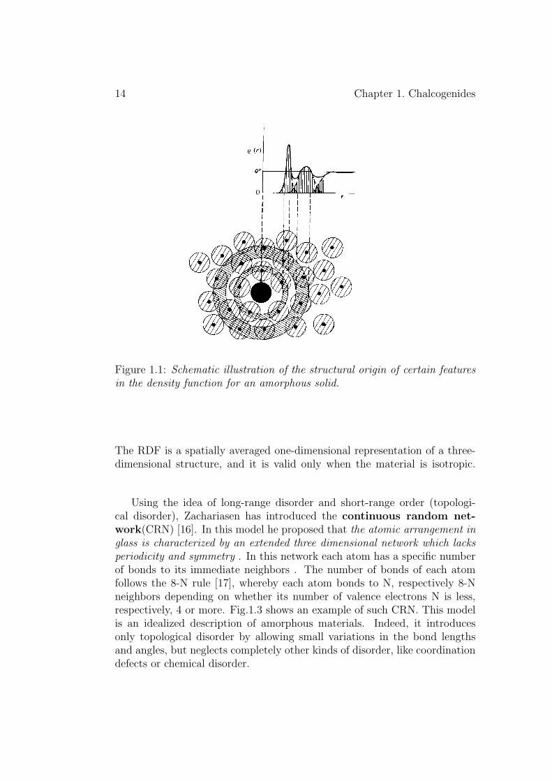
Figure 1.1: Schematic illustration of the structural origin of certain featuresin the density function for an amorphous solid.
The RDF is a spatially averaged one-dimensional representation of a three-dimensional structure, and it is valid only when the material is isotropic.
Using the idea of long-range disorder and short-range order (topologi-cal disorder), Zachariasen has introduced the continuous random net-work(CRN) [16]. In this model he proposed that the atomic arrangement inglass is characterized by an extended three dimensional network which lacksperiodicity and symmetry . In this network each atom has a specific numberof bonds to its immediate neighbors . The number of bonds of each atomfollows the 8-N rule [17], whereby each atom bonds to N, respectively 8-Nneighbors depending on whether its number of valence electrons N is less,respectively, 4 or more. Fig.1.3 shows an example of such CRN. This modelis an idealized description of amorphous materials. Indeed, it introducesonly topological disorder by allowing small variations in the bond lengthsand angles, but neglects completely other kinds of disorder, like coordinationdefects or chemical disorder.

1.1. Energy bands 15
Figure 1.2: Schematic illustration showing the relationship between short-range structural parameters: first and second-nearest neighbor bond lengths,r1 and r2, and bond angle θ as deduced from the first two peaks in the RDF.
Figure 1.3: (a)Representation of a hypothetical two-dimensional crystallineoxide A2O3, (b)The Zachariasen model for the amorphous form of the samecompound.
16 Chapter 1. Chalcogenides
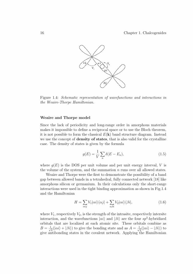
Figure 1.4: Schematic representation of wavefunctions and interactions inthe Weaire-Thorpe Hamiltonian.
Weaire and Thorpe model
Since the lack of periodicity and long-range order in amorphous materialsmakes it impossible to define a reciprocal space or to use the Bloch theorem,it is not possible to form the classical E(k) band structure diagram. Insteadwe use the concept of density of states, that is also valid for the crystallinecase. The density of states is given by the formula
g(E) =1
V
∑n
δ(E − En), (1.5)
where g(E) is the DOS per unit volume and per unit energy interval, V isthe volume of the system, and the summation n runs over all allowed states.
Weaire and Thorpe were the first to demonstrate the possibility of a bandgap between allowed bands in a tetrahedral, fully connected network [18] likeamorphous silicon or germanium. In their calculations only the short-rangeinteractions were used in the tight binding approximation as shown in Fig.1.4and the Hamiltonian
H =∑
αij
V1|αi〉〈αj|+ ∑
αβi
V2|αi〉〈βi|, (1.6)
where V1, respectively V2, is the strength of the intrasite, respectively intersiteinteraction, and the wavefunctions |αi〉 and |βi〉 are the four sp3-hybridizedorbitals that are localized at each atomic site. These orbitals combine asB = 1√
2(|αi〉+ |βi〉) to give the bonding state and as A = 1√
2(|αi〉 − |βi〉) to
give antibonding states in the covalent network. Applying the Hamiltonian
1.2. Bonding in amorphous semiconductors 17
to these wavefunctions gives two ranges of permitted energies. If V1/V2 < 0.5a bandgap Eg = 2|V2 − 2V1| arises between bonding and antibonding states;otherwise, the two energy ranges overlap. The importance of this modellies not in its quantitative use but in the fact that it did put an end tothe questioning if whether amorphous materials do or do not have a bandstructure, and that it showed the band structure to be mostly defined by theshort-range order.
1.1.3 Electron localization
It was shown above that small deviations (fluctuations) of bond lengths andangles from the crystalline values lead to topological disorder. This disordercauses two major effects in amorphous semiconductors. The first one istailing of permitted bands in the forbidden gap, which makes the band edgesless sharp than in the crystalline case, as sketched in Fig.1.5. The secondone is the localization of some of the electronic states, in the sense that anelectron lying in one of these states has a wavefunction amplitude that isalmost zero except in a limited space surrounding a particular lattice site;this is expressed by Ψ ∝ exp(−αr). It is important to point out that this isdifferent from extended states in crystalline materials where the amplitudeof the electronic wavefunction has a constant non-zero value through thecrystal; in this case the wavefunction is written Ψ ∝ exp(−ik.r).This effectis known as ”Anderson localization” [19].
If we have a band of width B, in the crystalline case, and a total energyrange W , in the amorphous case, over which the atomic potential fluctuates(Fig.1.6), a full localization for all one-electron states of the band can beproven if W/B > C [19] where C is a model-dependent constant.
In practice disorder in amorphous semiconductors is not large enough tolocalize all states of the valence and conduction bands [20][21]. It has beenshown that localization happens only in tail states and that there is a sharplimit between extended states and localized ones of the same band. This leadsautomatically to a sharp change in the carrier mobility value at energies Ev
and Ec. These two energies are called mobility edges, such that we can speakalso about the mobility gap in amorphous semiconductors besides the opticalone that reflects the tailing of states in the forbidden gap.
1.2 Bonding in amorphous semiconductors
When atoms form stable solids, it means that they are in favorable energyconfigurations. In covalent semiconductors this favorable low-energy state is

18 Chapter 1. Chalcogenides
Figure 1.5: (a)Parabolic DOS for a crystalline semiconductor ; (b) and (c)include the smearing-out of the band edges, which is caused by topologicaldisorder; in (c) localized states in the gap are caused by the bonding defects.
Figure 1.6: (a) Representation of potential wells for a crystalline lattice andthe density of states expected for a tight-binding model.(b) Representation ofthe potential wells of the Anderson model and the density of states expectedfor a tight-binding model.

1.2. Bonding in amorphous semiconductors 19
achieved through the formation of covalent bonds between outer electronsfrom neighboring sites. Such bonding lifts the degeneracy of the atomicenergy levels and produces a σ bonding orbital at lower energy and a raisedanti-bonding orbital σ∗. In the solid the number of atoms is very large whichcauses these states to broaden into bands.
The Mott 8 − N rule mentioned earlier [17] is the rule that covalentsemiconductors obey in bonding. For instence, the elements in column IVof the periodic table have an outer shell of 2s and 2p electrons. Since, inbonding, an atom strives to achieve a ”complete” N=8 outer shell, the columnIV element will form 4 highly directional sp3 hybridized orbitals, pointing tothe four corner of a tetrahedron, where they will link up with analogousorbitals from neighboring sites. Such bonding is assumed in the Weaire-Thorpe model, and defines the structure of semiconductors like silicon andgermanium. Elements of column VI such as the chalcogens (sulphur, seleniumand tellurium) have 6 electrons at the outer shell, 2 paired in an s state and4 in the p state, 2 of the latter are of course being paired. In this case eachatom makes two covalent bonds using the unpaired electrons in the p states.The paired electrons form the so-called lone-pair band that, as it will be seen,plays a crucial role in the properties of chalcogens and chalcogenides. Fig.1.7represents the electronic structure of an isolated chalcogen atom and a solidwhere the s , σ and lone-pair orbitals form the valence band (VB), and theσ∗ orbitals form the conduction band (CB). It is important to point out herethat the lone-pairs make up the top of the valence band.
1.2.1 Bonding defects in amorphous semiconductors
In crystalline semiconductors each atom is, in the ideal case, fully coordi-nated to its neighbors. However for the same semiconductor in its amorphousstate this is not the case. Due to the random distribution of bond lengthsand angles it can happen that an atom does not find the right number ofneighbors to satisfy its bonding requirement, in which case we can find anover-coordinated or under-coordinated atom. The former is characteristic forchalcogenides while the later is also found in tetrahedrally-bonded semicon-ductors like amorphous silicon and germanium.
It is well known that the typical defect in amorphous silicon is the dan-gling bond which is an sp3 orbital that does not participate in bonding. Thisdefect makes pure amorphous silicon not useful for any practical purposes.On the other hand, hydrogenated amorphous silicon occupies an importantplace in thin film transistors and solar energy cell applications. This is possi-ble because hydrogen passivates the dangling bonds and reduces the densityof states in the gap. Analogous neutral dangling bonds are not energetically

20 Chapter 1. Chalcogenides
Figure 1.7: (a) Electronic configuration of an isolated chalcogen atom. (b)When chalchogen atom bonds two of the four p-state electrons will help formtwo bonds while the two others do not participate in bonding and form a lonepair. The bonding leads to the appearance of the σ and σ∗ levels. (2 of the 8electrons are from a neighboring atom). (c) Solid-state interaction broadensthe atomic levels into bands.
favorable in chalcogenides, as will be shown below. This gives rise to a com-bination of charged under-coordinated and over-coordinated atoms to formthe energetically most favorable defects.
As a rule, the bonding defects create localized states that, energetically,lie in the forbidden energy gap. These states play an important role inthe electronic properties of amorphous semiconductors. When two electronsoccupy the same defect center the correlation energy between these electronswill have to be considered. It was found that this correlation energy is positivein tetrahedrally coordinated semiconductors and negative in chalcogenides.
Positive correlation energy
In tetrahedrally coordinated semiconductors a dangling bond has one un-paired electron and sits on a three-fold coordinated site. As this site iselectrically neutral, it is written as D0 and lies at the middle of the gapat the position of the sp3-hybridized atomic orbital. D0 is a paramagneticcenter and can be seen by the ESR technique. When the defect accepts asecond electron, it becomes a negatively charged one, written as D−, and theenergy of the level rises by an amount U (Hubbard energy) corresponding tothe Colombic repulsion between the two electrons. This case is typical for

1.2. Bonding in amorphous semiconductors 21
positive correlation energy defects.
Negative effective correlation energy
While the prominent ESR signal in tetrahedrally coordinated amorphoussemiconductor is an efficient tool to probe the defects density in these ma-terials, no equilibrium ESR signal has been detected in most of the chalco-genides 1 [22] [23]. This does not only mean that we lost a tool to probethe defects in chalcogenides, but it also gives rise to a fundamental questionas to why these materials do not show any spin resonance? A first expla-nation was given by Anderson [24]. Since the absence of an ESR signal atdark equilibrium, means that no significant amount of unpaired electrons arepresent in the material, he proposed that strong electron-phonon coupling inthe chalcogenides allowed doubly occupied sites to lower their energy belowthat of the singly occupied ones. Such polaronic deformation of the lattice isfacilitated by the two-fold coordination of the chalcogen atoms in the latticewhich makes the network very flexible. This flexibility is the key to explainthe lack of neutral dangling bonds D0, and thus unpaired electrons. Streetand Mott [25] filled in this idea as follows: The dangling bond in chalco-genides is doubly occupied and is therefore a negatively charged defect D−.Charge neutrality requires that D− should be compensated by another defecthaving the same density and the opposite charge state D+.
The harmonic lattice potential has a minimum at configuration coordinateq = 0 and can be written as
V =Cq2
2, (1.7)
where C is a constant. The lattice deformation due to electron-phonon in-teraction can be written as
Ep = −λq(n↑ + n↓), (1.8)
where λ is the electron-phonon coupling strength, and n↑ and n↓ are the siteoccupation number for an electron with spin up or down. Ep is a negativequantity and thus can allow lower energy at configuration coordinate q 6= 0.
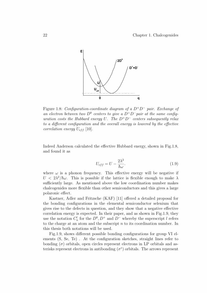
If two electrons are at the same defect the energy of the system will riseby the Coulombic positive repulsion energy (Hubbard energy) U = e2/4πεr,where ε is the dielectric function and r the distance between electrons. Innegative-U systems this Hubbard energy is more than compensated by theelectron-phonon interaction if the constant λ is large enough as it is shown inFig.1.8 which illustrates how the reaction 2D0 −→ D− + D+ is exothermic.
1However ESR signals are seen in the germanium sulfides.
22 Chapter 1. Chalcogenides
Figure 1.8: Configuration-coordinate diagram of a D+D− pair. Exchange ofan electron between two D0 centers to give a D+D−pair at the same config-uration costs the Hubbard energy U . The D+D− centers subsequently relaxto a different configuration and the overall energy is lowered by the effectivecorrelation energy Ueff [10].
Indeed Anderson calculated the effective Hubbard energy, shown in Fig.1.8,and found it as
Ueff = U − 2λ2
hω. (1.9)
where ω is a phonon frequency. This effective energy will be negative ifU < 2λ2/hω. This is possible if the lattice is flexible enough to make λsufficiently large. As mentioned above the low coordination number makeschalcogenides more flexible than other semiconductors and this gives a largepolaronic effect.
Kastner, Adler and Fritzsche (KAF) [11] offered a detailed proposal forthe bonding configurations in the elemental semiconductor selenium thatgives rise to the defects in question, and they show that a negative effectivecorrelation energy is expected. In their paper, and as shown in Fig.1.9, theyuse the notation C l
n for the D0, D+ and D− whereby the superscript l refersto the charge at an atom and the subscript n to its coordination number. Inthis thesis both notations will be used.
Fig.1.9, shows different possible bonding configurations for group VI el-ements (S, Se, Te) . At the configuration sketches, straight lines refer tobonding (σ) orbitals, open circles represent electrons in LP orbitals and as-terisks represent electrons in antibonding (σ∗) orbitals. The arrows represent

1.2. Bonding in amorphous semiconductors 23
Figure 1.9: Structure and energies of simple bonding configurations of groupVI elements. Straight lines represent bonds, small circles lone-pair (LP)electrons and asterisk the antibonding electrons. Arrows represent electronswith spin. The zero energy is the energy of LP [11].
electrons with spin up or down. With the energy of a LP taken as zero, theenergy per electron of a σ orbital is −Eb while the energy per electron in a σ∗
is Eb +∆, where ∆ > 0 because the antibonding states are always pushed upmore than the bonding states are pushed down. In all cases if an electron isadded to a Se atom it would be placed in a linear combination of σ∗ orbitalswith a correlation energy Uσ∗ which is smaller than the correlation energyULP if the added electron is placed on a lone-pair [11]. It is assumed that Eb
is much larger than ∆, Uσ∗ and ULP .
In the KAF notation a doubly coordinated Se atom would be written C02
and has an energy of −2Eb. The neutral three-fold coordinated atom C03
has an energy of −2Eb + ∆ but it is not stable as we will see below andthe neutral singly coordinated atom has an energy of −Eb. As it can beseen, the neutral dangling bond costs a full bond energy −Eb with respectto normal C0
2 while the C03configuration costs much less. Consequently, the
neutral dangling bond is energetically unfavorable. In other words, in a

24 Chapter 1. Chalcogenides
Figure 1.10: Visualisation of the three-fold coordinated D+ and singly coor-dinated D− defect centers (Valence Alternation Pair) by the exchange of anelectron between two D0 centers [10].
situation where disorder disrupts the normal C02 bonding, the C0
3 appearsto be the most likely defect configuration. However this C0
3 configurationis unstable. A charge transfer from one C0
3 configuration to another one bythe reaction 2C0
3 −→ C+3 + C−
3 would costs an energy Uσ∗ according to thescheme of Fig.1.9, but by breaking one of the three bonds, C−
3 spontaneouslybecomes an ordinary C0
2 while converting a nearest-neighbor C02 site into a
singly coordinated selenium atom with the extra electron, C−1 . The reaction
C−3 + C0
2 −→ C02 + C−
1 is exothermic if 2∆ − (ULP − Uσ∗) > 0. The sumof the two last reactions is 2C0
3 −→ C+3 + C−
1 , and in this way the systemlowers its energy by transferring two σ and two σ∗ electrons into LP statesof one singly-coordinated and one two-fold coordinated chalcogen. Becausethe creation of the two charged centers C+
3 C−1 is linked, they are known as
Valence Alternation Pairs, (VAP). A VAP creation mechanism is illustratedin Fig.1.10. It uses the neutral dangling bond as a precursor as suggested byStreet and Mott [25], contrary to the KAF proposal mentioned above wherethe neutral three-fold coordinated defect is the precursor. In either case thecharged centers that are created in the network lead to localized states in theforbidden gap that will be the subject of the next paragraph.
Energy levels of charged defects
The lattice deformation that causes the negative effective correlation energycauses charged defects to be characterized by different transitions energiesfrom and to the bands depending on the electron occupation of these defects.Taking into consideration that phonons can supply the necessary momentum

1.2. Bonding in amorphous semiconductors 25
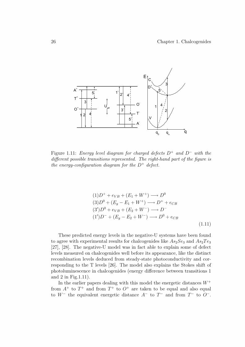
to accommodate the lattice deformation and photons cannot, there will bea difference between energies of optical and thermal transitions. To under-stand the different transitions involved in a negative-U system we can usethe Fig.1.11, where the the different possible transitions to and from D+ andD− defects are shown together with an energy-configuration diagram for theD+ defect.
The levels A+ and A− correspond to the charged defects at their equilib-rium configuration q0, these two levels are related to the optical transitions(1 and 1′) from the valence band to A+ and from A− to the conduction bandrespectively. The levels T and O represent thermal and optical transitionsinvolving the defects in their excited, electrically neutral states at changedconfiguration qn. Transitions 4 and 5 are thermal transitions between thevalence respectively conduction band and the D+ defect, bringing this defectback to its its D(+)0 configuration; the transition 4′ and 5′ are the similarones between the conduction respectively valence band and the D− defect.Transitions 2 and 3 correspond to photoluminescence and photoinduced ab-sorption respectively. In these transitions the D0 defect for instance, a neutraldangling bond, appears only as excited state of the charged defects.
The energy difference between T+(−) and A+(−) is W+(−), that is also theenergetic difference between T+(−) and O+(−) in the symmetric models usedin [11][25]. The energies E1 and E2 are defined by the equations:
D+ + e + (E1) −→ D0
D0 + e + (E2) −→ D−
Ueff = E2 − E1 < 0
Then the transitions involved in the negative-U model can be summarizedin this set of equations :
Thermal transitions
(4)D+ + eV B + (E1) −→ D0
(5)D0 + (Eg − E1) −→ D+ + eCB
(5′)D0 + eV B + (E2) −→ D−
(4′)D− + (Eg − E1) −→ D0 + eCB
(1.10)
Optical transitions
26 Chapter 1. Chalcogenides
Figure 1.11: Energy level diagram for charged defects D+ and D− with thedifferent possible transitions represented. The right-hand part of the figure isthe energy-configuration diagram for the D+ defect.
(1)D+ + eV B + (E1 + W+) −→ D0
(3)D0 + (Eg − E1 + W+) −→ D+ + eCB
(3′)D0 + eV B + (E2 + W−) −→ D−
(1′)D− + (Eg − E2 + W−) −→ D0 + eCB
(1.11)
These predicted energy levels in the negative-U systems have been foundto agree with experimental results for chalcogenides like As2Se3 and As2Te3
[27], [28]. The negative-U model was in fact able to explain some of defectlevels measured on chalcogenides well before its appearance, like the distinctrecombination levels deduced from steady-state photoconductivity and cor-responding to the T levels [26]. The model also explains the Stokes shift ofphotoluminescence in chalcogenides (energy difference between transitions 1and 2 in Fig.1.11).
In the earlier papers dealing with this model the energetic distances W+
from A+ to T+ and from T+ to O+ are taken to be equal and also equalto W− the equivalent energetic distance A− to T− and from T− to O−.

1.2. Bonding in amorphous semiconductors 27
This assumption has no physical ground as can be seen in the comparison ofexperimental and theoretical results given in [27].
Over the three decades since the negative-U energy-level scheme was pro-posed it has found support in a wide range of experimental results (see forexample [27] [28]). Nevertheless, some dissenting voices have been heard.Based on theoretical calculations, Vanderbilt and Joannopoulos [13] con-cluded that a-Se is a positive correlation energy system. In this calculation asuperlattice containing the charged defects in question was used. The super-lattice is constructed of supercells of 12 atoms, each containing 2 C0
1 centersin one calculation or C+
3 and C−1 centers in the next one. The effective en-
ergy Ueff = U(C+3 C−
1 )−U(2C01) was found to be positive. The problem with
this study is that the superlattice is unrealistically small to represent a-Se,and that 25% of defect sites is unrealistically high. Tanaka [29] on the otherhand has questioned the presence of charged defects in chalcogenides on thebasis of optical absorption measurements on highly purified As2S3 samples.However, the lack of extra optical absorption at the energy levels predictedby the negative-U model is not a sufficient argument to doubt the validity ofthis model in chalcogenides [12]. Indeed, absorption by the wide band tailsgenerated in As2S3 by homopolar As−As bonds can easily mask absorptionby underlying charged defects.
1.2.2 Behavior of the Fermi level
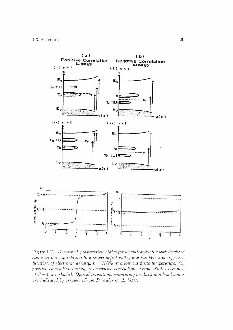
Serious efforts have been made in the past to dope the chalcogenide semi-conductors [30], all without success. Nevertheless, it was reported that it ispossible to make certain germanium selenides n-type by doping (the betterword will be alloying in this case) with about 10% of Bi or Pb [31], [32].The fact that the Fermi level stays pinned in the neighborhood of midgap,a characteristic property of the chalcogenides, was argued by Adler [33] asfollows:
Consider that we have a semiconductor with valence and conduction bandedges, Ev and Ec, and an empty defect giving rise to localized states in thegap at energy T0.Extra carriers are then introduced in the system. For amaterial with a positive correlation energy the doubly occupied states arehigher in energy than the singly occupied states. As electrons are injectedinto the system they populate the unoccupied states at energy T0. Conse-quently, the Fermi level shifts gradually in the band around T0 due to theaverage chemical potential at which the additional electron would be located(Fig.1.12).a. When the number of electrons per defect n becomes 1, wheren = N/N0 and N is the total number of electrons associated with the defectstates and N0 is the total number of defects [33] ( this means that all defects
28 Chapter 1. Chalcogenides
are singly occupied), all other injected electrons would have to create doublyoccupied states at higher energy T0 + U . At this condition the Fermi leveljumps discontinuously from the T0 into the T0 + U band, and rises graduallyin this band until n = 2, as shown in the part a of the lower frames in thesame figure. All states are then doubly occupied.
In the case of negative correlation energy systems, the results are totallydifferent. The doubly occupied state has the lower energy position in the gapsuch that, as electrons are injected into the system, they first populate anunoccupied state giving rise to a singly occupied level (an unoccupied state +e), and then this singly occupied level becomes doubly occupied one by beingpopulated by the next injected electron. (a doubly occupied state = a singlyoccupied state + e). Thus this level falls in energy band at T0−U , as shownin Fig.1.12.b. The number of doubly occupied states is proportional to thenumber of electrons introduced into the system. Since this band of defectlevels is always full, we conclude that in this system the Fermi level will bepinned midway between the energies T0 and T0 − U over the whole range ofoccupation number n, as shown in part b of the lower half of Fig.1.12.
1.3 Selenium
As mentioned in the introduction, Se is the oldest semiconductor that physi-cists have deal with. Its golden age coincided with its application in reprog-raphy in Xerox machines, but its economic importance decreased drasticallyafter introduction of silicon and organic semiconductors in this application.The new usage of Se as an X-ray-sensitive material in digital X-ray imag-ing detectors has brought renewed interest, while also reminding us that ourknowledge about a-Se is poor. Here we summarize some of its characteristics.
1.3.1 Microstructure of selenium
Selenium has five crystalline states [30], the more important of which are thehexagonal and monoclinic ones.
Hexagonal Se which is always referred to as Seγ, is the most stable formof selenium. The crystal is made up of parallel helical chains, as shown inFig.1.13, where every atom has two nearest neighbors from the same chainsituated at a distance 2.30 A −2.37 A and four neighbors from the otherchains situated at a distance 3.42 A - 3.48 A. While the interaction betweenchains is of the Van der Waals type, the atoms are covalently bonded withinthe same chain. The hexagonal unit cell contains three atoms and the latticeparameters at 18 C are a = 4.3544 A, c=4.9496 A, c/a=1.1367 [30]; the
1.3. Selenium 29
Figure 1.12: Density of quasiparticle states for a semiconductor with localizedstates in the gap relating to a singel defect at T0, and the Fermi energy as afunction of electronic density, n = N/N0 at a low but finite temperature: (a)positive correlation energy; (b) negative correlation energy. States occupiedat T = 0 are shaded. Optical transitions connecting localized and band statesare indicated by arrows. (From D. Adler et al. [33]).
30 Chapter 1. Chalcogenides
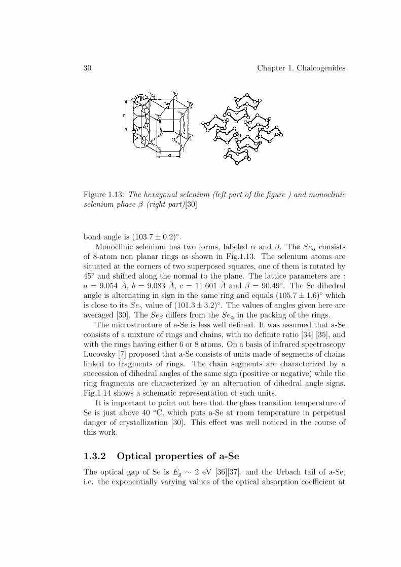
Figure 1.13: The hexagonal selenium (left part of the figure ) and monoclinicselenium phase β (right part)[30]
bond angle is (103.7± 0.2).Monoclinic selenium has two forms, labeled α and β. The Seα consists
of 8-atom non planar rings as shown in Fig.1.13. The selenium atoms aresituated at the corners of two superposed squares, one of them is rotated by45 and shifted along the normal to the plane. The lattice parameters are :a = 9.054 A, b = 9.083 A, c = 11.601 A and β = 90.49. The Se dihedralangle is alternating in sign in the same ring and equals (105.7± 1.6) whichis close to its Seγ value of (101.3± 3.2). The values of angles given here areaveraged [30]. The Seβ differs from the Seα in the packing of the rings.
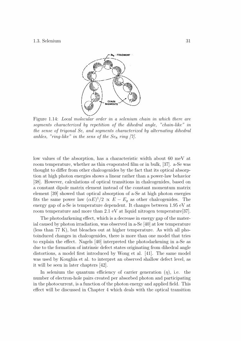
The microstructure of a-Se is less well defined. It was assumed that a-Seconsists of a mixture of rings and chains, with no definite ratio [34] [35], andwith the rings having either 6 or 8 atoms. On a basis of infrared spectroscopyLucovsky [7] proposed that a-Se consists of units made of segments of chainslinked to fragments of rings. The chain segments are characterized by asuccession of dihedral angles of the same sign (positive or negative) while thering fragments are characterized by an alternation of dihedral angle signs.Fig.1.14 shows a schematic representation of such units.
It is important to point out here that the glass transition temperature ofSe is just above 40 C, which puts a-Se at room temperature in perpetualdanger of crystallization [30]. This effect was well noticed in the course ofthis work.
1.3.2 Optical properties of a-Se
The optical gap of Se is Eg ∼ 2 eV [36][37], and the Urbach tail of a-Se,i.e. the exponentially varying values of the optical absorption coefficient at
1.3. Selenium 31
Figure 1.14: Local molecular order in a selenium chain in which there aresegments characterized by repetition of the dihedral angle, ”chain-like” inthe sense of trigonal Se, and segments characterized by alternating dihedralanhles, ”ring-like” in the sens of the Se8 ring [7].
low values of the absorption, has a characteristic width about 60 meV atroom temperature, whether as thin evaporated film or in bulk, [37]. a-Se wasthought to differ from other chalcogenides by the fact that its optical absorp-tion at high photon energies shows a linear rather than a power-law behavior[38]. However, calculations of optical transitions in chalcogenides, based ona constant dipole matrix element instead of the constant momentum matrixelement [39] showed that optical absorption of a-Se at high photon energiesfits the same power law (αE)1/2 ∝ E − Eg as other chalcogenides. Theenergy gap of a-Se is temperature dependent. It changes between 1.95 eV atroom temperature and more than 2.1 eV at liquid nitrogen temperature[37].
The photodarkening effect, which is a decrease in energy gap of the mater-ial caused by photon irradiation, was observed in a-Se [40] at low temperature(less than 77 K), but bleaches out at higher temperature. As with all pho-toinduced changes in chalcogenides, there is more than one model that triesto explain the effect. Nagels [40] interpreted the photodarkening in a-Se asdue to the formation of intrinsic defect states originating from dihedral angledistortions, a model first introduced by Wong et al. [41]. The same modelwas used by Koughia et al. to interpret an observed shallow defect level, asit will be seen in later chapters [42].
In selenium the quantum efficiency of carrier generation (η), i.e. thenumber of electron-hole pairs created per absorbed photon and participatingin the photocurrent, is a function of the photon energy and applied field. Thiseffect will be discussed in Chapter 4 which deals with the optical transition
32 Chapter 1. Chalcogenides
involved in the negative-U model.
1.3.3 Electronic properties
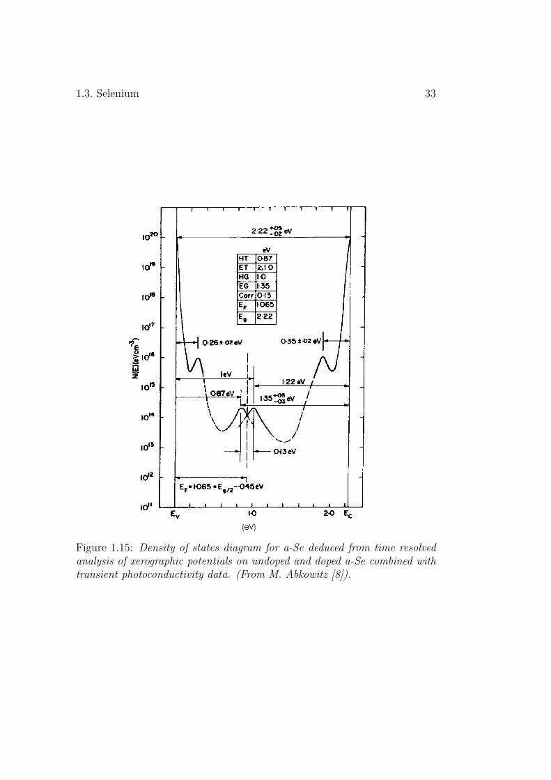
As is the case for other chalcogenides, holes are the more mobile chargecarriers in a-Se [43][9]. Their mobility is around thirty times the electronicone. At low temperature, the hole mobility is dependent on the appliedelectric-field while the electronic one is field-independent [9]. It is well knownthat the DOS is the key to understand the electrical transport propertiesof amorphous materials. However, for a-Se the DOS model proposed byAbkowitz [8], shown in Fig.1.15, has serious deficiencies as will be discussedlater. It is required, therefore, that a more firmly-based specification of thea-Se DOS be elaborated.
It may be remarked that a very specific model for the negative-U centersis available for a-Se [11], but with the experimental positioning of the de-fect levels in the bandgap not yet resolved, while the reverse situation holdsfor other chalcogenides. For instance: Negative-U energy levels are well es-tablished for As2Se3 [28] [27], but the actual atomic configurations of thecharged defects remain in doubt [44]. Elliott [10] has mentioned that sev-eral parameters make Se an anomalous material in a number of ways. Oneof these parameters is the Se dielectric constant which is approximately halfthe value of other chalcogenides. Consequently, the repulsive energy betweentwo electrons on the same defect site is high, and its compensation is lessprobable, thus conceivably making double occupancy less likely. The lack ofESR signal could then be interpreted through the sensitivity of a-Se for un-wanted additives like chlorine or oxygen that might compensate the defects[10]. It is clear from the above that defining the DOS of a-Se and answeringthe question whether it is a negative- or positive-U system are related prob-lems. Experimentally we can detect the defect levels in the gap of a-Se bythe photoconductivity techniques that will be discussed in the next chapter.
1.3. Selenium 33
Figure 1.15: Density of states diagram for a-Se deduced from time resolvedanalysis of xerographic potentials on undoped and doped a-Se combined withtransient photoconductivity data. (From M. Abkowitz [8]).

34 Chapter 1. Chalcogenides
Chapter 2
Photoconductivity techniques
In this chapter the photoconductivity in semiconductors will be introduced,i.e the increase of the conductivity under optical excitation, as an experimen-tal tool to probe the electronic properties of the material. Indeed, the extrafree charge carriers created by the photon absorption will contribute to theelectronic transport under an applied electric field. They will interact withmaterial defects, and at the end these extra charge carriers are injected in theexternal circuit or just recombine in different ways. Two different regimescan be discussed in the photocurrent. First there is the transient one andsecondly the steady state. In both cases the photocurrent forms the basis ofseveral experimental techniques, part of which have been used in this studyof a-Se.
2.1 General concepts
When the appropriate light strikes a semiconductor, it generates free chargecarriers. The total free-electron and free-hole concentrations n and p aregiven by :
n = n0 + ∆n,
p = p0 + ∆p, (2.1)
where n0 and p0 are the thermal equilibrium concentrations and ∆n and ∆pare the extra free carrier concentrations generated by the light. Then thephotoconductivity is given by :
∆σ = e(µn∆n + µp∆p), (2.2)
where µn and µp are the electron and hole mobility and e is the electroncharge. Technically there are several ways to prepare a sample for photocon-
35
36 Chapter 2. Photoconductivity techniques
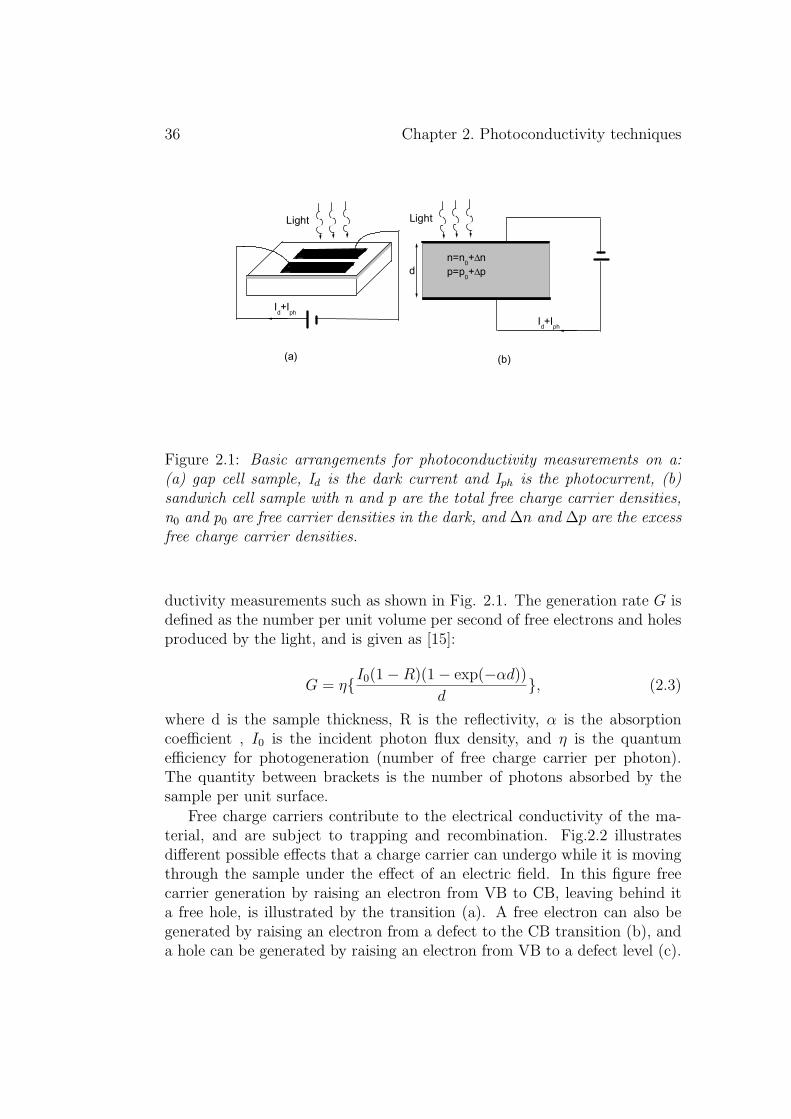
Figure 2.1: Basic arrangements for photoconductivity measurements on a:(a) gap cell sample, Id is the dark current and Iph is the photocurrent, (b)sandwich cell sample with n and p are the total free charge carrier densities,n0 and p0 are free carrier densities in the dark, and ∆n and ∆p are the excessfree charge carrier densities.
ductivity measurements such as shown in Fig. 2.1. The generation rate G isdefined as the number per unit volume per second of free electrons and holesproduced by the light, and is given as [15]:
G = ηI0(1−R)(1− exp(−αd))
d, (2.3)
where d is the sample thickness, R is the reflectivity, α is the absorptioncoefficient , I0 is the incident photon flux density, and η is the quantumefficiency for photogeneration (number of free charge carrier per photon).The quantity between brackets is the number of photons absorbed by thesample per unit surface.
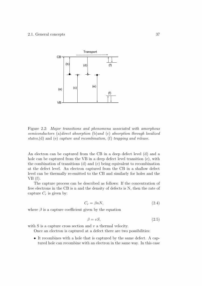
Free charge carriers contribute to the electrical conductivity of the ma-terial, and are subject to trapping and recombination. Fig.2.2 illustratesdifferent possible effects that a charge carrier can undergo while it is movingthrough the sample under the effect of an electric field. In this figure freecarrier generation by raising an electron from VB to CB, leaving behind ita free hole, is illustrated by the transition (a). A free electron can also begenerated by raising an electron from a defect to the CB transition (b), anda hole can be generated by raising an electron from VB to a defect level (c).
2.1. General concepts 37
Figure 2.2: Major transitions and phenomena associated with amorphoussemiconductors (a)direct absorption (b)and (c) absorption through localizedstates,(d) and (e) capture and recombination, (f) trapping and release.
An electron can be captured from the CB in a deep defect level (d) and ahole can be captured from the VB in a deep defect level transition (e), withthe combination of transitions (d) and (e) being equivalent to recombinationat the defect level. An electron captured from the CB in a shallow defectlevel can be thermally re-emitted to the CB and similarly for holes and theVB (f).
The capture process can be described as follows: If the concentration offree electrons in the CB is n and the density of defects is N, then the rate ofcapture Cr is given by:
Cr = βnN, (2.4)
where β is a capture coefficient given by the equation
β = vS, (2.5)
with S is a capture cross section and v a thermal velocity.Once an electron is captured at a defect there are two possibilities:
• It recombines with a hole that is captured by the same defect. A cap-tured hole can recombine with an electron in the same way. In this case

38 Chapter 2. Photoconductivity techniques
the defect is called a recombination center. This recombination processis called indirect recombination, in contrast to the direct recombinationwhere an electron falls directly from the CB to the VB.
• It can be thermally excited to the CB to participate again in the elec-tronic transport and in this case the defect is called a trap. The phe-nomena of capturing in a trap (trapping) and release from it (detrap-ping) play an important role in the electronic transport in amorphoussemiconductors. Indeed, a charge carrier moves through the semicon-ductor in the extended states in the lapse of time between the lastdetrapping and the next trapping event, which means the charge car-rier is free when moving.
Whether a center (defect level) is to be considered as trapping center ora recombination center depends on the probability for the charge carrier(electron) to be thermally ejected to the conduction band or to recombinewith the opposite charge carrier. If the recombination probability is largerthan the release probability, the defect is a recombination center. A centeracts as a trap under specific conditions and as a recombination center underother conditions; the delimitation between the two is defined by the quasi-Fermi levels, which will be discussed later.
If attention is restricted to the recombination at a density of recombina-tion centers N with capture coefficient β, the average time the carrier (in thiscase the electron) is free before recombination is given by the equation:
τ =1
βN. (2.6)
Combining this equation with Eq.2.4 gives that the capture rate Cr, whichbecomes in this case a recombination rate, is equal to n/τ . In the steadystate regime the density of free electrons n is constant, which means thatthe rate of generation is equal to the rate of recombination and this happenwhen [45]:
n = Gτ. (2.7)
When a semiconductor is in a thermal equilibrium the occupation prob-ability of a state at energy E is given by the Fermi-Dirac distribution:
f(E) =1
1 + exp(E−EF0
kT), (2.8)
where EF0 is the equilibrium Fermi level, k the Boltzmann constant and Tthe temperature. The free electron and hole densities at thermal equilibrium
2.1. General concepts 39
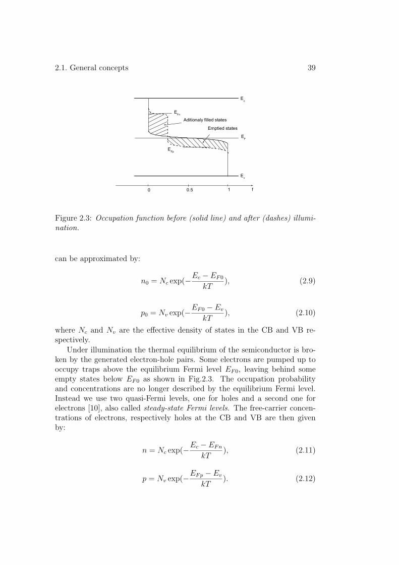
Figure 2.3: Occupation function before (solid line) and after (dashes) illumi-nation.
can be approximated by:
n0 = Nc exp(−Ec − EF0
kT), (2.9)
p0 = Nv exp(−EF0 − Ev
kT), (2.10)
where Nc and Nv are the effective density of states in the CB and VB re-spectively.
Under illumination the thermal equilibrium of the semiconductor is bro-ken by the generated electron-hole pairs. Some electrons are pumped up tooccupy traps above the equilibrium Fermi level EF0, leaving behind someempty states below EF0 as shown in Fig.2.3. The occupation probabilityand concentrations are no longer described by the equilibrium Fermi level.Instead we use two quasi-Fermi levels, one for holes and a second one forelectrons [10], also called steady-state Fermi levels. The free-carrier concen-trations of electrons, respectively holes at the CB and VB are then givenby:
n = Nc exp(−Ec − EFn
kT), (2.11)
p = Nv exp(−EFp − Ev
kT). (2.12)
40 Chapter 2. Photoconductivity techniques
Figure 2.4: Schematic time development of the excess carrier concentration∆n in response to a period of illumination.
When the semiconductor is irradiated the electron quasi-Fermi level isabove the equilibrium Fermi level EF0, while the other one is below it. Theenergetic distance between a quasi-Fermi level and the equilibrium one isproportional to the light intensity and inversely proportional to the temper-ature. When the irradiation is stopped the two quasi Fermi levels collapse tothe equilibrium EF0. It may be noted that the occupancy function involv-ing the quasi-Fermi levels has similar form as the equilibrium Fermi-Diracdistribution function.
It is customary to define demarcation levels between the shallower energylevels that will trap and re-emit carriers and the deeper levels where a trappedcarrier has a higher probability of recombining with a carrier of the oppositesign, rather than being re-emited. To first approximation, these demarcationlevels can be identified with the quasi-Fermi levels. The states lying betweenthe two demarcation levels are taken as recombination centers. When theconcentration of free charge carriers n and p is increased, the two demarcationlevels are separated further giving rise to more recombination of carriers.
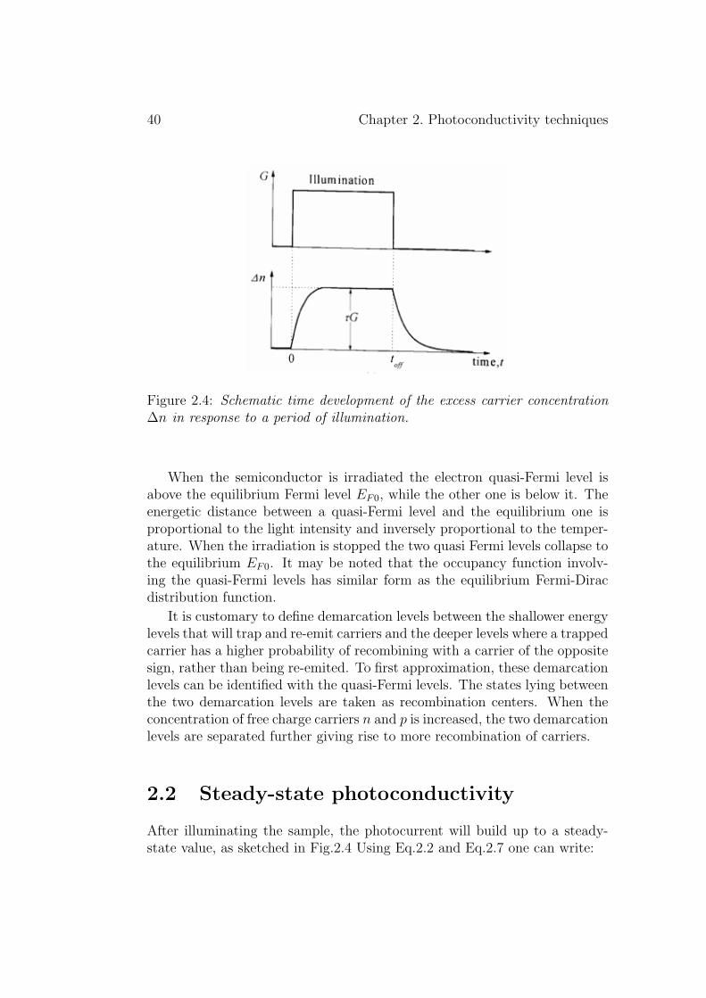
2.2 Steady-state photoconductivity
After illuminating the sample, the photocurrent will build up to a steady-state value, as sketched in Fig.2.4 Using Eq.2.2 and Eq.2.7 one can write:
2.2. Steady-state photoconductivity 41
∆σ = eG(µnτn + µpτp), (2.13)
where τn and τp are the average lifetimes of electrons and holes respectively.If one term in the last equation is much larger than the other one, which isthe case in chalcogenides where the hole term dominates, then the photocon-ductivity can be written as:
∆σ = eGµpτp. (2.14)
When it can be assumed that the absorption is uniform through thesemiconductor, and that reflectivity is small enough to be neglected, thenthe photogeneration rate can be written as G = ηαI0 and the steady-statephotoconductivity becomes:
∆σ = eµpτpηαI0. (2.15)
In this equation the two parameters α and η represent the effect of pho-togeneration on the photoconductivity while the two parameters µp and τp
represents the effect of transport.
2.2.1 Effect of light intensity
It was experimentally observed that in chalcogenides the photocurrent atsmall light excitation intensities, I0, and/or high temperatures, grows lin-early with I0, while at high light intensities and/or low temperatures thephotocurrent is proportional to the square root of I0.This can be summa-rized in the following equation:
Iph ∝ Iγ : 1 ≥ γ ≥ 0.5. (2.16)
The current dependence on light intensity (called Lux-Ampere characteris-tics) has been widely studied [26][46][47], and was found to have a close rela-tionship with the type of recombination involved in the process. Informationabout the DOS can also be deduced as we will see later.
Weiser [46] proposed a model to explain the Lux-Ampere characteristicsin chalcogenides. Consider a semiconductor where the electrical transport isdominated by one type of carrier, and with only one type of recombinationcenter. Under optical excitation an extra density of holes ∆p is generatedwith generation rate G. If the material is assumed to be intrinsic such asn0 = p0 and that ∆n = ∆p, the rate of change of the excess carriers ∆p isgiven by:

42 Chapter 2. Photoconductivity techniques
d(∆p)
dt= G− [βNr(p0 + ∆p)− βp2
0], (2.17)
where Nr is the concentration of the recombination centers. In steady-state,d(∆p)/dt = 0, and under the conditions mentioned above (an intrinsic semi-conductor with one type of recombination centers) Nr = p0 + ∆p, giving:
G = β(∆p2 + 2p0∆p). (2.18)
At low intensity ∆p ¿ p0, meaning that thermally excited carriers p0 aredominant, Eq.2.18 becomes
∆p =G
2βp0
, (2.19)
from where we can write:
Iph ∝ σph ∝ ∆p ∝ G ∝ I0 (2.20)
In this case the recombination type is referred to as monomolecular .At high light intensity ∆p À p0, the thermally excited carriers can be
neglected and the Eq.2.18 becomes:
∆p = (G
β)
12 . (2.21)
It can then be written :
Iph ∝ σph ∝ ∆p ∝ (G
β)
12 ∝ (I
120 ), (2.22)
in which case the recombination type is referred to as bimolecular .It is now established that by changing light intensity the recombination
changes from one regime to another (changes of γ between 1 and 0.5). Inter-mediate values of γ between 1 and 0.5 indicate that photo-excited carriershave approximately the same density as the thermally excited ones.
2.2.2 Effect of temperature
Experimentally it was seen that in traditional chalcogenide semiconductors,like As2Se3, photoconductivity in function of temperature has a maximumat temperature T = Tm separating two regimes:
• at temperatures T > Tm the photocurrent Iph is generally lower thanthe dark current Id. In this range Iph increases exponentially with
2.2. Steady-state photoconductivity 43
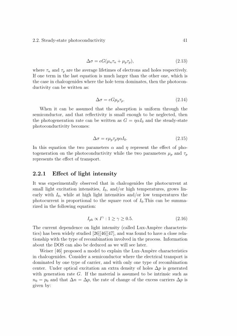
Figure 2.5: Temperature dependence of steady-state dark Id and photocurrentIph in bulk a-As2Se3 gap cell at different light intensities [48].
1/T and changes linearly with light intensity I0, (the monomolecularregime).
• at temperatures T < Tm the photocurrent Iph is higher than the darkcurrent Id, it decreases exponentially with 1/T , and varies as the squareroot of the light intensity I0 (bimolecular regime).
The temperature Tm, corresponding to the photocurrent maximum, movesto lower temperatures with decreasing light intensity, and this can be ex-plained by the fact that an increase in temperature reduces the energeticdistance between the quasi-Fermi levels, analogous to the effect of decreasinglight intensity. These effects are observed in Fig.2.5.
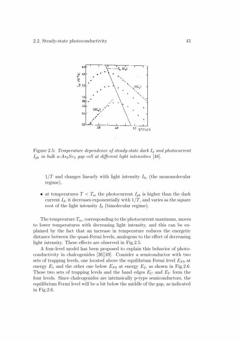
A four-level model has been proposed to explain this behavior of photo-conductivity in chalcogenides [26][49]. Consider a semiconductor with twosets of trapping levels, one located above the equilibrium Fermi level EF0 atenergy E1 and the other one below EF0 at energy E2, as shown in Fig.2.6.These two sets of trapping levels and the band edges EC and EV form thefour levels. Since chalcogenides are intrinsically p-type semiconductors, theequilibrium Fermi level will be a bit below the middle of the gap, as indicatedin Fig.2.6.
44 Chapter 2. Photoconductivity techniques
Figure 2.6: Schematic description of the four levels model.
In the references [26][49] the free and trapped carrier densities under op-tical excitation are obtained by solving the rate equations for the changes inoccupation of the four levels in terms of the transition rates of charge carriers(electrons and holes) into and out of a particular level. The photocurrent de-duced in the the 4-level model does show the two ranges of interest indicatedabove:
• The range corresponding to low light level and characterized by thefact that p0 À ∆p. In this range the photocurrent increases linearlywith the generation rate G (monomolecular regime), and increases ex-ponentially with 1/T with activation ∆Em/k [49]. In this regime theextra steady state density of holes (to which the photocurrent is pro-portional) is given by:
∆p = (G
vSNt
) exp(+∆Em
kT), (2.23)
where v is thermal velocity, Nt the density traps and S is the hole cap-ture cross section for the trap. ∆Em is defined differently in the calcu-lations of Simmons [49] and those of Main [26]. While Main calculatesthe result as ∆Em = 1
2(E1−E2), Simmons uses ∆Em = Eσ−(E2−Ev),

2.3. Optical absorption coefficient 45
where Eσ is the activation energy of the thermally activated dark cur-rent which, to first approximation, equals EF . Since EF itself liesroughly in mid-gap, the difference in the results in not significant.
• The range corresponding to high light level and characterized by thefact that ∆p À p0. In this range the photocurrent increases as thesquare root of the generation rate G (bimolecular regime), is decreasingexponentially with increasing 1/T , and has an activation energy ∆Eb/k.The density of photoexcited holes is given in this case by:
∆p = (GN0
vSNt
)12 exp(−∆Eb
kT), (2.24)
where N0 is the density of states at the band edges Ec and Ev, and∆Eb = 1
2(E2 − Ev).
The experimental observations are in agreement with this model. The setof two localized states are located experimentally by measuring the three pa-rameters Eσ, ∆Em and ∆Eb, which define the energetic positions E1and E2 ofFig.2.6. It was mentioned earlier that this set of localized states is congruentwith the charged defect levels of the negative-U model in chalcogenides.
It is important to note here that this does not mean that other possibledefect levels do not exist in the material. Moreover this image is idealizedbecause every set of traps in amorphous semiconductors is spread out arounda mean energy, and the band edges are ”smeared out” by tailing.
2.3 Optical absorption coefficient
The optical absorption coefficient is tightly related to the DOS in the sub-gap energy range of a semiconductor, and SSPC can be used in a number ofways to measure this optical absorption coefficient. If the optical flux I0 iswritten as I0 = I/hν then the photoconductivity will be written as:
∆σ(E) = eµpτ(I/hν)(1−R)ηα(E). (2.25)
If the parameters η, R and µ are energy-independent, a direct determi-nation of α(E) from ∆σ(E) can be made by measuring ∆σ as a function ofphoton energy using the SSPC experimental setup. Of course, care should betaken to fulfill the validity conditions of Eq.2.25, i.e the maximum photon-energy used is less than the energy gap of the semiconductor. Any featurein the DOS, lying in the experimental energy range, will be reflected in thisabsorption spectrum. However, in a-Se η is energy-dependent, and thus α
46 Chapter 2. Photoconductivity techniques
cannot be measured directly, but the photocurrent spectral response, that isthe photocurrent at different wavelengths for the same number of photons,can be used for the same goal.
The constant photocurrent method (CPM) was proposed by Vanecek andco-workers [50][51] to measure α as a function of energy. In CPM the pho-tocurrent is kept constant by continuous adjustment of the light intensity Iwhile the photon energy is scanned across the spectrum, which means thatthe positions of the quasi-Fermi levels are immobile and thus the free carrierlifetime τ is constant. The required light intensity in this case is inverselyproportional to the number of photogenerated free charge carriers. For a-Seand using the Eq.2.25 with the assumption that R and µ are energy inde-pendent the parameter αη can be measured, and information about the DOScan be drawn from that.
In both above techniques, a convolution of the two sides of the bandgapDOS is probed, just as is the case with standard optical spectroscopy. Re-solved features close to the band edge may, therefore, point to defects ineither VB or CB tail.
2.4 Transient photocurrent techniques
The study of transient aspects of photoconductivity can relate to either thebuild-up or relaxation of steady-state photocurrents, or to a material’s re-sponse to pulsed excitation. The SSPC turn-on transient reflects the inter-play between generation and recombination of carriers. This interplay canlead to a current overshoot as has been seen seen with some low-temperatureresults. A special focus in this work will be on the transient photocurrentsafter a pulsed laser flash, involving both the traditional transient photocon-ductivity (TPC) and time-of-flight (TOF) techniques. The transient pho-tocurrents can be interpreted in terms of a multiple-trapping (MT) model.
2.4.1 Time-of-flight technique
The TOF technique involves the creation and drift of a thin layer of ex-cess charge carriers (holes or electrons) through the thickness of a sandwich-cell configuration of a semiconductor sample. It was first used by Spear tomeasure the drift mobility of carriers in a-Se [52], where a short pulse ofhigh-energy electrons was used to create the layer of excess charge carriersjust beneath the top contact. It was adapted from the original techniqueby Haynes and Shockley [53] who measured the drift mobility in long crys-talline rods of semiconductors. Nowadays the creation of the excess charge

2.4. Transient photocurrent techniques 47
carriers is achieved through the use of a short laser flash (nanoseconds andless). The fact that in the TOF technique only one type of charge carrierscan be drifted at a time, depending on the applied field, gives to it a specialimportance because it provides the opportunity to separately probe the DOSat the CB side as well as the VB side. While the excess charge carriers aredrifted through the sample, they interact with the trap and recombinationcenters in the band gap. This interaction creates a relationship between thetransient current in this technique and the DOS of the material, and thusthe opportunity to probe the electronic properties of the material studied.When most of the excess carriers leave the sample at the back contact, thetransient photocurrent drops abruptly, but a measurable current can stillbe seen due to carrier release from deep traps. This ”post-transit” currentmakes it possible to study those deep traps.
Physical validity conditions
• In order to be able to see a transit time tT , which corresponds to thearrival of a representative part of the excess charge carriers at the backcontact, the dielectric relaxation time τe of the semiconductor shouldbe much larger than the transit time τe À tT . Thus, the highly resistivesemiconductors are suitable for this purpose because τe = ρε0εr, whereρ is the semiconductor resistivity, εr is its relative permittivity and ε0
the dielectric constant. The low dark current is a result of the aboveconditions and it makes the photocurrent more distinguishable andmeasurable. It was shown that the influence of the dielectric relaxationtime on the post-transit photocurrent is minimal [54][55].
• To obtain a representative drift mobility, excess charge carriers mustbe drifted across the sample with a constant drift velocity, (vd). Thisrequires a uniform applied electric field Fa which is achieved by applyinga pulsed voltage Va to the sample before triggering the laser flash [52].The creation and drifting of an excess carrier layer through the sampleperturbs the uniformity of the applied field. However, it is possibleto minimize this uniformity perturbation by making the total createdexcess charge much less than the equilibrium charge CVa on the samplecapacitance. Indeed, at time t < tT the system can be described as twocapacitors in series, as shown in Fig.2.7, the upper one with chargeQ′−Ne ,where N is the number of excited carriers, under a field F1(x)and the lower one with charge Q′ under a field F2(x), these two electricfields are given by the following equations:

48 Chapter 2. Photoconductivity techniques
Figure 2.7: Schematic representation of the TOF experiment. The layer ofexcess carriers Ne with a drift velocity vd perturbs the applied field Fa =V a/d, resulting in fields F1 and F2. The excess carriers are created in a thinlayer δ under the top contact.
F1(x) = Fa − Ne
εA(1− x
d), (2.26)
F2(x) = Fa +Ne
εA
x
d, (2.27)
where A is the surface of the capacitor (contact) and d the thickness. Ifthe total excess carrier charge is small enough with respect to the equi-librium capacitor charge Ne ¿ Q = CVa, the field will be consideredas constant F1 ' F2 ' Fa.
• In the ideal case the distribution of the created excess carrier layershould be a delta function, Gδ(x)δ(t). The laser flash, on the order ofnanoseconds in length fulfills the condition of the very short distributionin time, while an appropriate wavelength of the laser flash, stronglyabsorbed in the material, ensures the narrow distribution in space.Indeed, if this is not the case the laser flash will be absorbed throughoutthe semiconductor which causes a spread in the arrival time of thecarriers at the back contact and a large uncertainty on the measuredtransit time. Care has to be taken as well to avoid the absorption atvery shallow depth in the semiconductor where the excess charges canrecombine in the highly defective surface layer. No useful transientTOF photocurrent is obtained in that case.
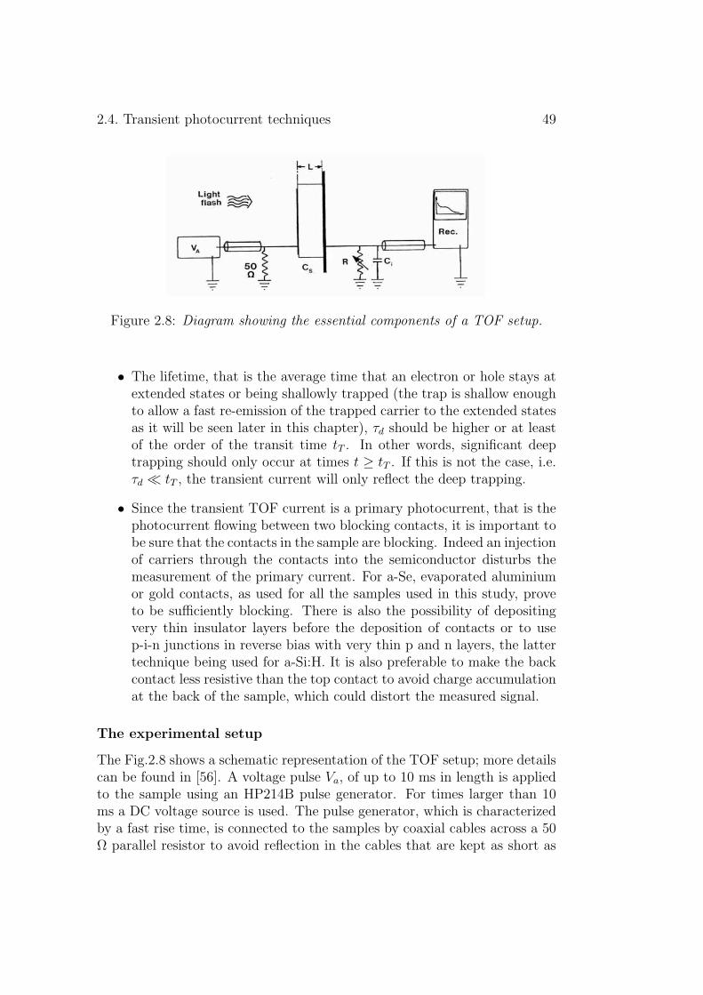
2.4. Transient photocurrent techniques 49
Figure 2.8: Diagram showing the essential components of a TOF setup.
• The lifetime, that is the average time that an electron or hole stays atextended states or being shallowly trapped (the trap is shallow enoughto allow a fast re-emission of the trapped carrier to the extended statesas it will be seen later in this chapter), τd should be higher or at leastof the order of the transit time tT . In other words, significant deeptrapping should only occur at times t ≥ tT . If this is not the case, i.e.τd ¿ tT , the transient current will only reflect the deep trapping.
• Since the transient TOF current is a primary photocurrent, that is thephotocurrent flowing between two blocking contacts, it is important tobe sure that the contacts in the sample are blocking. Indeed an injectionof carriers through the contacts into the semiconductor disturbs themeasurement of the primary current. For a-Se, evaporated aluminiumor gold contacts, as used for all the samples used in this study, proveto be sufficiently blocking. There is also the possibility of depositingvery thin insulator layers before the deposition of contacts or to usep-i-n junctions in reverse bias with very thin p and n layers, the lattertechnique being used for a-Si:H. It is also preferable to make the backcontact less resistive than the top contact to avoid charge accumulationat the back of the sample, which could distort the measured signal.
The experimental setup
The Fig.2.8 shows a schematic representation of the TOF setup; more detailscan be found in [56]. A voltage pulse Va, of up to 10 ms in length is appliedto the sample using an HP214B pulse generator. For times larger than 10ms a DC voltage source is used. The pulse generator, which is characterizedby a fast rise time, is connected to the samples by coaxial cables across a 50Ω parallel resistor to avoid reflection in the cables that are kept as short as

50 Chapter 2. Photoconductivity techniques
possible.A time delay generator triggers a VSL-337 nitrogen laser, via a 20 m long
coaxial cable, 80 µs after the start of the voltage pulse. The laser pulses are3 ns long, have an energy of 120 µJ , and a wavelength of 337 nm. The laserpumps a dye cell with Coumarin 440 A dissolved in ethanol that gives byfluorescence a 440 nm wavelength light pulse of 5 ns duration. The intensityof this light pulse can be, if necessary, reduced by neutral density filters.To avoid disturbance to the electrical circuit, the laser source is placed in acopper box that it-self is in an aluminium enclosure, both of them acting asFaraday cages. This light pulse is highly absorbed in a-Se and can create asuitable layer of excess carriers for TOF experiments.
An IWATSU-8123 digitizing oscilloscope is used to record the currents,measured repeatedly on different time scales to extend the range and keepsufficient resolution (on logarithmic scale) . At first the voltage pulse isapplied, followed, after 80 µ s to avoid distortion of the signal by the RC timeconstant of the measuring circuit (sample included), by a light pulse and thetotal current is measured. Next the voltage pulse is repeated and the darkcurrent recorded. The desired photocurrent is the result of subtracting thedark current from the total current. The measured quantity is the voltagedrop across a variable load resistor R placed across the scope input. Actuallya 50 Ω resistor is used at short time scales, and this resistor is increasedstepwise till 500 KΩ to measure lower and lower photocurrents at longertimes. The total transient TOF photocurrent signal consists of the overlapof all photocurrents measured at successive time scales [56]. It is importantto point out that the RC constant of the circuit should be sufficiently small.A proper balance between the contact area, thickness of the sample, and itsdielectric constant will keep the sample capacitance low.
The sample is mounted in a cryostat that can be evacuated during mea-surements, and where the temperature of the sample can be kept constantat a chosen value between 150 K and 400 K, through a combination of cool-ing and heating. The former is done with a cold finger immersed in liquidnitrogen, and the latter is done with an electrical filament wound around thetop of the copper rod that forms the cold finger. The temperature regulationwithin 0.5 K is achieved by controlling the current through the filament.
2.4.2 Transient photocurrent
In the standard TPC, a coplanar sample configuration (gap cell) is used, thusboth electrons and holes participate in the measured current. A DC voltageV is applied to the sample, followed by a light flash that creates extra chargecarriers distributed in the bulk of the sample within a depth depending on
2.4. Transient photocurrent techniques 51
the wavelength used. It is preferable to avoid highly absorbed light and thusstrong absorption at the surface of the sample since this is highly defectiveand does not reflect the bulk properties of the studied material. Under theinfluence of the applied field the extra charges (electrons and holes) movethrough the sample until their eventual disappearance through recombina-tion, but before this happens they will have been immobilized a numberof times by various traps that are present in the semiconductor. Throughthese interactions, the measured photocurrent contains information aboutthe DOS of the material. Experimentally the same setup described above forTOF technique is used.
2.4.3 Multiple-trapping transport model
As described above, when a distribution of excess charge carriers is generatedin an amorphous semiconductor, the carriers will eventually leave the sampleor recombine. In between these two events, creation and leaving or recombi-nation, it is assumed that the carriers move in the extended states and can betrapped once or several times in traps lying at different energies in the bandgap of the semiconductor, from where they will be thermally re-emitted to theextended states. The time that each carrier spends in a trap depends on theenergy position of this trap according to t = ν−1exp(Et/kT ) where ν is theattempt-to-escape frequency, Et is the energy of the trap, k the Boltzmannconstant and T the temperature. These effects are illustrated for an electronin the Fig.2.9. Such transport mechanism is called the multiple-trappingtransport model, or trap-limited band transport, and can be used to inter-pret experimental results of different transient photoconductivity techniquessuch as TOF and TPC. This mechanism of transport is dominant in amor-phous semiconductors at relatively high temperatures (above 150 K) but itis less dominant at low temperatures, where other transport mechanisms likehopping between localized states dominate.
The equations that describe MT are written for a system with M trappinglevels as:
∂n
∂t+
∂fn
∂x= G(x, t) +
M∑
i=1
rini − nM∑
i=1
ωi, (2.28)
∂ni
∂t= nωi − rini, (2.29)
where n is the density of free carriers, ni is the density of carriers trappedat an energy level Ei, ri is the release rate from traps situated at Ei, ωi isthe capture rate (probability per unit time) in traps at Ei, G(x, t) is the
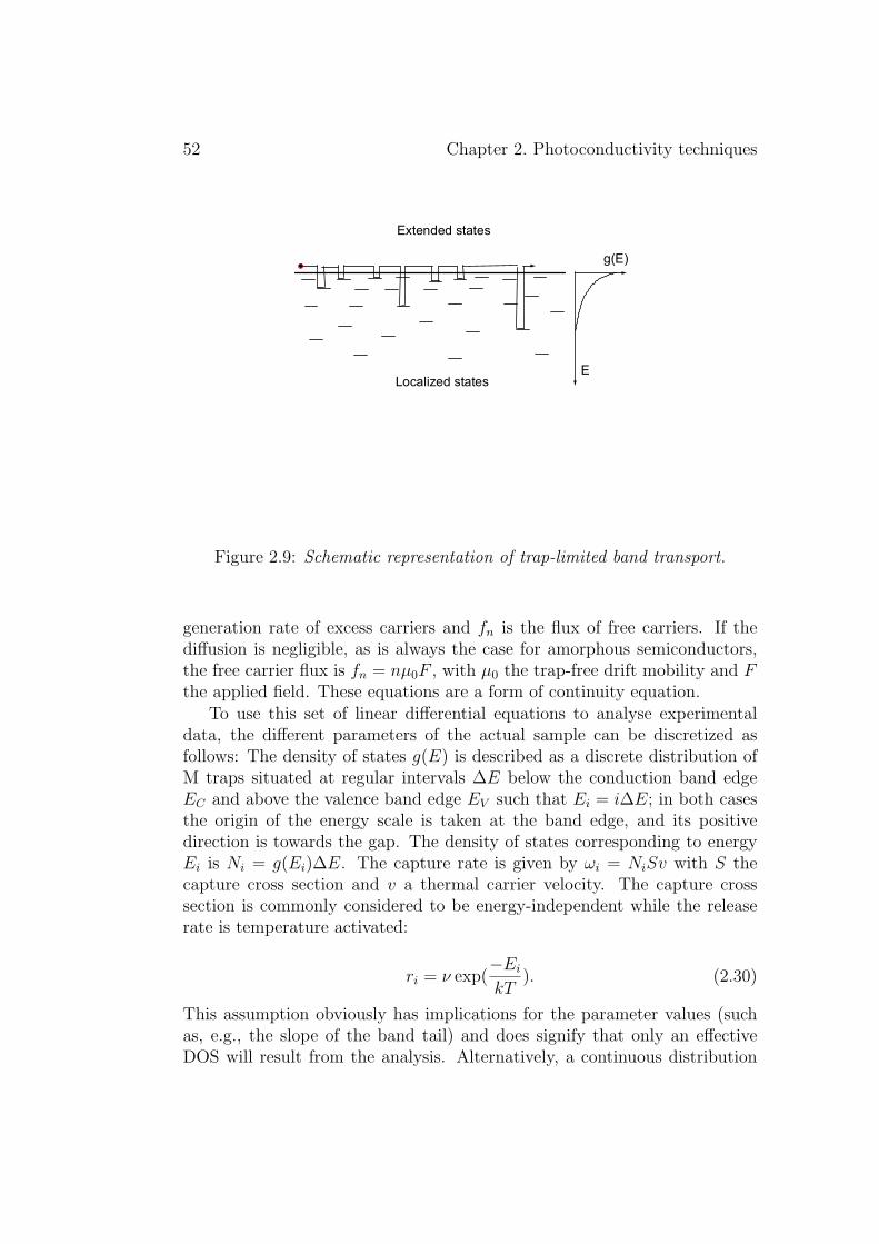
52 Chapter 2. Photoconductivity techniques
Figure 2.9: Schematic representation of trap-limited band transport.
generation rate of excess carriers and fn is the flux of free carriers. If thediffusion is negligible, as is always the case for amorphous semiconductors,the free carrier flux is fn = nµ0F , with µ0 the trap-free drift mobility and Fthe applied field. These equations are a form of continuity equation.
To use this set of linear differential equations to analyse experimentaldata, the different parameters of the actual sample can be discretized asfollows: The density of states g(E) is described as a discrete distribution ofM traps situated at regular intervals ∆E below the conduction band edgeEC and above the valence band edge EV such that Ei = i∆E; in both casesthe origin of the energy scale is taken at the band edge, and its positivedirection is towards the gap. The density of states corresponding to energyEi is Ni = g(Ei)∆E. The capture rate is given by ωi = NiSv with S thecapture cross section and v a thermal carrier velocity. The capture crosssection is commonly considered to be energy-independent while the releaserate is temperature activated:
ri = ν exp(−Ei
kT). (2.30)
This assumption obviously has implications for the parameter values (suchas, e.g., the slope of the band tail) and does signify that only an effectiveDOS will result from the analysis. Alternatively, a continuous distribution

2.4. Transient photocurrent techniques 53
Figure 2.10: The thermalization process for electrons as a function of time.The trapped charge is represented by the shadded area. (a) Immediate chargetrapping after photocreation; (b) E∗ sinks deeper in the gap as time goes on;(c) carrier distribution for T > TC .
can replace the summation over discrete levels of Eq.2.28 as demonstratedby Arkhipov et al [57]. A simplified analysis of transient currents in MTcontext was worked out by Tiedje and Rose [58] and Orenstein and Kastner[59] (TROK). They used, implicitly or explicitly, the thermalization conceptthat allows the distinction between thermalized states and non-thermalizedones. For an amorphous semiconductor with a DOS that has an exponentialshape g(E) = g(Ec = 0) exp(−E/kTc), where kTc is the characteristic widthof the conduction band tail (a similar analysis can be done with holes, themore mobile carriers in chalcogenides), and assuming that the transport is astatistical process with an energy-independent capture cross section S. Withenergy-independent capture, the initial distribution of trapped carriers isproportional to the DOS. As time goes on, the shallowly trapped carriers arethermally re-emitted to the extended states while deeper trapped carriershave to wait longer, in function of the trap depth, to be released; at the sametime the trapping of previously released carriers remains random and thustrapped carriers accumulate at the deeper states. The thermalization energy,that is the limit between shallow and deep states at any moment, is definedas the energy where the release time r−1(E∗) is equal to the time elapsedafter the laser pulse, t = ν−1
0 exp(E∗/kT ), and thus the expression :
E∗(t) = kT ln(ν0t). (2.31)
54 Chapter 2. Photoconductivity techniques
All the states above E∗(t) are in quasi-thermal equilibrium with the extendedstates (valence band in the case of holes) while the states below the E∗(t)are not as shown in Fig.2.10. For temperatures T < TC the concentrationof occupied states exhibits a sharp peak at E∗(t) that, progressively, movesto greater depths as time elapses . The concept of thermalization can beextended to non-exponential DOS [60]. In the case where Tc < T the densityof trapped carriers does not show the same sharp peak at E∗ as shown inFig.2.10.c.
Since the time spent by a carrier in a trap at energy Ei is an exponentialfunction of this energy, differences in energetic positions of traps lead to bigdifferences in the transit time for individual carriers depending on which trapor traps they visited before completing their transit. Thus the original thinlayer of excess carriers has become spread out at the arrival to the backcontact in a TOF experiment (much more than the spread that would becaused by diffusion in a trap-free semiconductor). In this case the transportis called dispersive.
The trap-free mobility is reduced in amorphous materials by the timethat carriers spend in traps and thus the drift mobility is
µd = µ0τf
τf + τt
, (2.32)
where the subscript f refers to a free and the subscript t refers to a trappedcarrier. The last equation can be written in function of trapped and free car-rier densities, and taking in account that trapped carriers largely outnumberthe free ones in amorphous semiconductors, as follows:
µd = µ0nf
nf + nt
' µ0nf
nt
. (2.33)
Interpretation of TOF transient currents
Within the conditions of validity of a TOF experiment the generation rateG can be written as G(x, t) = G0δxδt. By using the appropriate boundaryconditions the set of Eq.2.28 and 2.29 can be solved for n(x, t) and ni(x, t)viainverse Laplace transforms. In the TROK approximation and for T < Tc themobility can be treated as a two-level problem, the first one at the bandedge (E = 0) where nf is defined, and the second one at the time dependentenergy E∗ (Eq.2.31) where the maximum of the trapped carriers density nt islocated. Like all other quantities, nf is time-dependent and for an exponen-tial DOS, it decreases with time as tα−1, where α is defined as the dispersionparameter and given by α = T/Tc. From Eq.2.33 it follows that µd is alsotime dependent and that a carrier crosses the sample with a time-dependent
2.4. Transient photocurrent techniques 55
average drift speed vd(t) = µd(t)F . The transit time tT corresponds to thetime that carriers having the above average drift speed need to reach theback contact, and thus:
d =∫ tT
0µd(t)Fdt. (2.34)
The above power-law decay of transient TOF photocurrent I ∼ nf only lastsuntil the transit time tT :
I(t < tT ) ∼ t−(1−α); (2.35)
at longer times, the photocurrent decreases according to the steeper power-law:
I(t > tT ) ∼ t−(1+α). (2.36)
According to the TROK model, the parameter α is the same for the twopower laws. However in experimental results it was noticed that it is notthe case and that it has two values α1 for the first power law and α2 for thesecond, and that they obey different temperature dependencies. This canbe attributed to the failure of the simplified exponential distribution of tailstates. The pre-transit photocurrent decay is due to the decrease in densityof free carriers associated with the progressive thermalization and randomtrapping, while the steeper decay in the photocurrent at the post-transitregion is due to extraction of carriers from the sample through the backcontact.
It follows from Eq.2.34 and the assumption of an exponential DOS thattT has a non-linear dependence on field and sample thickness of the form:
tT ∼ (d
F)
1α . (2.37)
Also the TOF drift mobility that is calculated from tT by the formula
µd =d2
tT Va
, (2.38)
will therefore have a non-linear dependence on field and sample thickness.These relationships should be used to estimate the parameter α, rather thanthe power law of the pre-transit current of the TOF signal because in theformer data as a function of both temperature and field are used, while inthe latter data are in function of temperature only.
56 Chapter 2. Photoconductivity techniques
Experimentally, it was further found that, to first approximation, thedrift mobility at fixed field is thermally activated according to the equation:
µd ∝ exp(−Ea
kT), (2.39)
where the activation energy Ea corresponds to the deepest energy level thata trapped carrier can be released from on average at the transit time tT . It isalso reported that this activation energy is field dependent, the higher fieldgiving the lower activation energy. This is caused by the higher velocity offree carriers under the higher field, leading to fewer trapping events duringthe carrier transit, thus preventing the demarcation level from reaching thesame energetic depth as for the lower field [61][62]. Michiel et al. reportedthat the activation energy becomes field-independent when the distribution ofstates is too steep or when the DOS contains a sharp feature that dominatesthe transport [63].
Interpretation of TPC transients
The analysis of standard TPC experimental data sets in the MT formalismfollows closely the above analysis for the TOF signals. Although TPC usesthe gap-cell geometry while TOF makes use of sandwich cells, pulsed opticalexcitation is employed in both instances to create a reservoir of free carriersat t=0. Those carriers then thermalize in and drift through the sample. Infact both pre-transit TOF analysis and TPC give the same t−(1−α) powerlaw for the exponential DOS. With respect to the TPC signal, a furtherdevelopment has been the study of the current behavior when a sharp featureis superimposed on the exponential DOS [64] [65]. Such feature producesa kink in the current trace; from its temperature dependence the energyposition of the feature can be deduced.
The pre-transit current in a TOF experiment on a thick sample can betreated as the standard photocurrent decay in a gap cell configuration sample,and it can show the same behavior described above.

Chapter 3
Thermal transitions in thenegative-U energy scheme fora-Se
As was mentioned in Chapter 1, the thermally accessible localized state levelsT+ and T− can be detected using either transient or steady-state photo-conductivity techniques. This chapter will deal with these levels related tothe negative-U model in a-Se using TOF, TPC and SSPC techniques. Thedetection of the T+ and T− levels will be a first step to answer the questionwhether a-Se is a negative-U system or not.
3.1 Steady-state photoconductivity
Often steady-state photoconductivity is the simplest technique to probe therecombination levels in the gap of chalcogenide amorphous semiconductors.However, for a-Se the situation is more complicated since the range of temper-atures where we can see the change of recombination mode from bimolecularto mono-molecular is narrow. Indeed, as it was mentioned above, the glasstransition temperature of a-Se is around 42 C. Another problem in this senseis that a-Se is a highly sensitive photoconductor, and thus it is difficult tomeasure photocurrents lower in magnitude than the dark current.
3.1.1 Experimental results
Experimental conditions
DC conductivity measurements were carried out in a 5×10⁻³ Pa atmosphereby means of a Keithley 428 current amplifier and an Agilent 3440a millivolt-
57

58 Chapter 3. Thermal transitions
meter, with a suitable applied voltage for every sample. For measuring thesteady-state photoconductivity (SSPC), a 15 mW He-Ne laser (632.8 nm)or an infra-red light emitting diode (LED), 890 nm, 1.7 mW/cm2 at 50 mAwere used as monochromatic light sources. Calibrated neutral density filtersserved to modify the light intensity.
a-Se films with thickness varying from 1 to 20 µm were evaporated ina vacuum background of 10−2 Pa from 99.995% pure Se (Alfa Aesar) ontohigh-resistivity Corning 7059 glass substrates. For the measurements, eithergap-cell or sandwich-cell configurations were used. Gap cells had evaporatedgold electrodes on top of the films with active areas of 0.5 mm × 10 mm.Aluminium electrodes were used for one bulk sample. The substrate temper-ature was not regulated during the evaporations, but X-ray examination ofseveral films proved that they were fully amorphous. A further set of samplesdeposited on either glass or aluminium substrates and with Au and Pt topcontacts was provided by Prof. Kasap (University of Saskatchewan). Theirthickness ranged from 8 to 300 µm. From this set, a 265 µm thick sandwichsample deposited on aluminium and provided with top gold contact, wasused for the steady-state measurements.
During SSPC measurements, the sample is placed on a metal support inthe vacuum chamber. The sample temperature is controlled to better than0.5 K by a combination of liquid nitrogen cooling and regulated electricalheating of the sample support.
Results
Fig.3.1 shows data sets for the temperature dependence of the steady-statephoto- and dark currents as follows:
• The 265 µm thick a-Se sandwich cell, when illuminated at 890 nm withthe LED is shown in Fig.3.1.a. The change-over from rising currentswith rising inverse temperature at the high-temperature end to decreas-ing currents at the low-temperature end corresponds to the traditionalpattern observed in numerous chalcogenide glasses [28][26][30]. At thehigher temperatures, i.e. at high concentrations of thermally generatedcarriers, monomolecular recombination controls the magnitude of thephotocurrent [26] and the activation energy, ∆Em, of the photocurrentin that range indicates the position above the material’s Fermi level ofa donor-like recombination center. At the low-temperature side, theoptically generated carriers will dominate the conductivity, the recom-bination will be mostly bimolecular, and the photocurrent activationenergy in this region, ∆Eb, can be linked to an acceptor-like recombi-nation center located 2∆Eb above the valence band mobility edge [26].
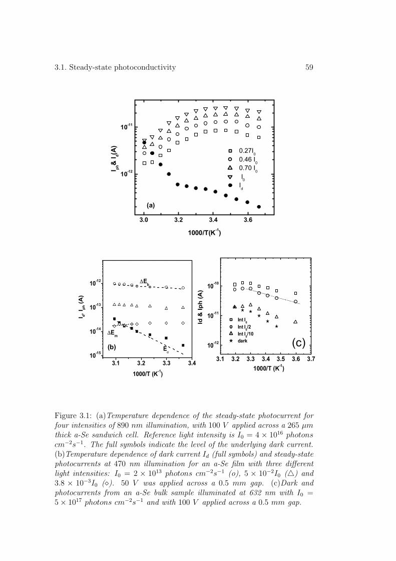
3.1. Steady-state photoconductivity 59
Figure 3.1: (a)Temperature dependence of the steady-state photocurrent forfour intensities of 890 nm illumination, with 100 V applied across a 265 µmthick a-Se sandwich cell. Reference light intensity is I0 = 4 × 10¹⁶ photonscm−2s−1. The full symbols indicate the level of the underlying dark current.(b)Temperature dependence of dark current Id (full symbols) and steady-statephotocurrents at 470 nm illumination for an a-Se film with three differentlight intensities: I0 = 2 × 10¹³ photons cm−2s−1 (o), 5 × 10⁻²I0 (4) and3.8 × 10−3I0 (¦). 50 V was applied across a 0.5 mm gap. (c)Dark andphotocurrents from an a-Se bulk sample illuminated at 632 nm with I0 =5× 10¹⁷ photons cm−2s−1 and with 100 V applied across a 0.5 mm gap.
60 Chapter 3. Thermal transitions
From Fig.3.1.a, ∆Em = (0.50 + 0.02) eV can be determined with goodprecision, but the temperature range available below the photocurrentmaximum is too limited to permit the determination of ∆Eb with sim-ilar precision. Consequently, the value of ∆Eb has to be deduced fromother measurements where a larger temperature range is available.
The dark conductivity data shown in Fig.3.1.a testify to the presenceof two different conduction mechanisms in the sample. For 103/T < 3.2K−1, an activation energy of 0.92 eV is observed, in general agreementwith results from other samples and with reported literature values inthe 0.9 to 1.0 eV range. To first approximation this energy reflects theenergetic distance EF−EV between the valence band mobility edge andthe Fermi level (holes being the mobile carriers in the chalcogenides),and indicates that band transport dominates. At lower temperatures ahopping current component is dominant with the approximate activa-tion energy of 0.25 eV reflecting injection across the aluminium oxidebarrier at the bottom contact of the sample. Depending on the indi-vidual sample, the magnitude of this injected current can vary widely,but the activation energy remains the same.
• The open symbols in 3.1.b show the temperature dependence of thephotocurrent in an a-Se gap cell in a logIph versus 103/T diagram forthree different light intensities: I, 1, 5×10⁻²I and 3.8×10⁻³I, where I =2×10¹³ photons/cm2s represents the full light intensity at 470 nm (2.64eV ) illumination. At low temperatures and high light intensities, i.e.when the photocurrent is larger than the dark current, a bimolecularrecombination regime leads to an exponentially decreasing Iph with1/T . Activation energy value,∆Eb of 0.13 eV is found. More resultsnot presented in this thesis, but to be found in [66], have given a ∆Eb
value of 0.17 eV.
• Similar temperature dependencies of the photocurrent are found in bulkstabilized a-Se samples. However, the transition between the mono-and bimolecular recombination regimes is now more spread out in tem-perature since successively deeper-lying layers of the bulk sample willbe subject to increasingly lower illumination intensities. The opticallyexcited free carrier density will thus vary through the sample while thethermally excited, dark, density remains constant. Fig.3.1.c shows anexample of such transition. A He-Ne laser (632.8 nm) was substitutedfor the 470 nm excitation used above in order to moderate the vari-ation in optical excitation density. While the ∆Eb slope (∼ 0.28 eV)is readily available, and the transition to a different regime is seen, no
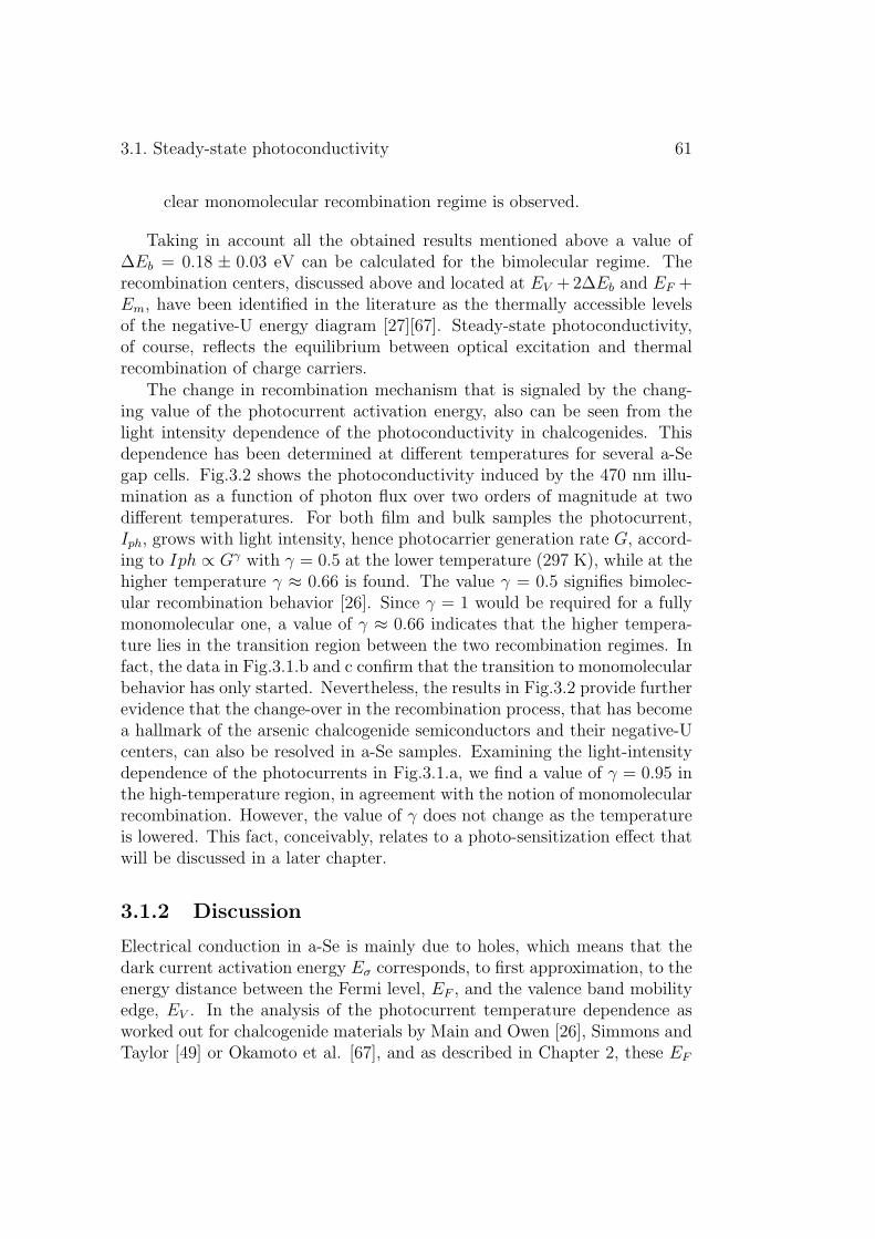
3.1. Steady-state photoconductivity 61
clear monomolecular recombination regime is observed.
Taking in account all the obtained results mentioned above a value of∆Eb = 0.18 ± 0.03 eV can be calculated for the bimolecular regime. Therecombination centers, discussed above and located at EV +2∆Eb and EF +Em, have been identified in the literature as the thermally accessible levelsof the negative-U energy diagram [27][67]. Steady-state photoconductivity,of course, reflects the equilibrium between optical excitation and thermalrecombination of charge carriers.
The change in recombination mechanism that is signaled by the chang-ing value of the photocurrent activation energy, also can be seen from thelight intensity dependence of the photoconductivity in chalcogenides. Thisdependence has been determined at different temperatures for several a-Segap cells. Fig.3.2 shows the photoconductivity induced by the 470 nm illu-mination as a function of photon flux over two orders of magnitude at twodifferent temperatures. For both film and bulk samples the photocurrent,Iph, grows with light intensity, hence photocarrier generation rate G, accord-ing to Iph ∝ Gγ with γ = 0.5 at the lower temperature (297 K), while at thehigher temperature γ ≈ 0.66 is found. The value γ = 0.5 signifies bimolec-ular recombination behavior [26]. Since γ = 1 would be required for a fullymonomolecular one, a value of γ ≈ 0.66 indicates that the higher tempera-ture lies in the transition region between the two recombination regimes. Infact, the data in Fig.3.1.b and c confirm that the transition to monomolecularbehavior has only started. Nevertheless, the results in Fig.3.2 provide furtherevidence that the change-over in the recombination process, that has becomea hallmark of the arsenic chalcogenide semiconductors and their negative-Ucenters, can also be resolved in a-Se samples. Examining the light-intensitydependence of the photocurrents in Fig.3.1.a, we find a value of γ = 0.95 inthe high-temperature region, in agreement with the notion of monomolecularrecombination. However, the value of γ does not change as the temperatureis lowered. This fact, conceivably, relates to a photo-sensitization effect thatwill be discussed in a later chapter.
3.1.2 Discussion
Electrical conduction in a-Se is mainly due to holes, which means that thedark current activation energy Eσ corresponds, to first approximation, to theenergy distance between the Fermi level, EF , and the valence band mobilityedge, EV . In the analysis of the photocurrent temperature dependence asworked out for chalcogenide materials by Main and Owen [26], Simmons andTaylor [49] or Okamoto et al. [67], and as described in Chapter 2, these EF

62 Chapter 3. Thermal transitions
Figure 3.2: The dependence of the photocurrent on the light intensity, at twotemperatures, for a-Se film (open symbols) and bulk (full symbols) samples.
and EV levels serve as references for the energy positions of the recombinationcenters that dominate in either the monomolecular or the bimolecular recom-bination regime. At high temperatures and low illumination intensities, thephotocurrent defines the energy location in the gap of a discrete donor-likerecombination center as E1 = EV + EF + ∆Em. The high-temperature pho-tocurrent in turn locates an acceptor-like recombination center at the energyE2 = EV + 2∆Eb. In chalcogenides these centers can be identified with thenegative-U centers, i.e. the charged defects with negative effective electroncorrelation energy [15][10]. In selenium, these are thought to be a three-foldcoordinated positively charged selenium atom C+
3 and singly coordinatednegatively charged one C−
1 .
Applying the above relationships to our steady-state photoconductivityresults for a-Se, the energy values deduced are E2 − EV = (0.36 ± 0.06)eV and E1 − EV = (1.42 ± 0.02) eV for the thermal transitions involvingnegative-U defects. With respect to the conduction band, the E1 level findsitself at EC − E1 = (0.53± 0.02) eV if the accepted gap value of Eg = 1.95eV is used. The 0.36/0.53 eV set of levels, thus obtained with respect tothe bands are closer to the theoretical values of Eg/4 ≈ 0.5 eV than to theearlier 0.26/0.35 eV set proposed in [8] and shown in Fig.1.15. These earlier
3.1. Steady-state photoconductivity 63
values are in fact based on a misinterpretation of the original TOF data setsof Kasap and Juhasz [9]. Indeed, in analogy to the pioneering work on TOFin chalcogenides by Marshall and Owen [68], it was assumed in [8] that theactivation energy of the drift mobility corresponds to the energy positionin the bandgap of a prominent trapping center. Marshall [69] has sinceshown that such interpretation is unwarranted, and that a field dependenceof the drift mobility as seen for a-Se does actually signal a broad featurelessdistribution of traps in the relevant energy range.
As can be seen in Fig.3.1, experimental conditions affect the results con-siderably. One of these experimental factors is the use of short-wavelengthlight in a gap-cell configuration which allows surface states to play a role inthe recombination, while longer wavelengths, as used with the sandwich cellconfiguration, permit to reduce the influence of these surface states and makethe illumination more homogenous through the sample bulk. A clear limi-tation is the restricted temperature range over which SSPC measurementscan be made on the high temperature side of the photoconductivity maxima.The low glass transition temperature of a-Se is responsible for that limit. Itis important to mention that the nice monomolecular recombination regimeseen in Fig.3.1.a is measured above glass-transition temperature, and withinfrared light excitation in a very thick sandwich sample. Care was takento measure at temperatures above the glass transition temperature for briefperiods only to avoid any unwanted crystallization of the material. Never-theless, in spite of this limitation , it was possible to see the change from oneregime to the other in all measured samples. This sensitivity to experimentalconditions does explain the scatter in data deduced from measurements ondifferent samples, as shown by the set selected for Fig.3.1.
Results deduced in this work are totally different from a set of steady-state photocurrent measurements that resolved a linear dependence of thephotocurrent on the light intensity for all temperatures and wavelengths [70].However, the latter should not be trusted because the data were obtainedwith 60 nm thin films deposited on glass. Although the substrate is notmentioned in [70], contemporary papers by the same group [71] indicate theuse of glass substrates, and the resulting dark current activation energy of0.7 eV clearly refers to Na ionic conductivity in the substrate [72] rather thanthe a-Se film on top.
At temperatures below the ones discusses in this section, a defect levelsituated just above the Fermi level can causes a sensitization effect, whichleads to an increase in photocurrent at lower temperature (with maximumaround −20 C) As will be seen in later chapter, this photocurrent featurecan affect the photocurrent slope in the bimolecular recombination regime.
The two defect levels that were identified above, can be probed by other
64 Chapter 3. Thermal transitions
techniques as well. Among them are the transient photocurrent techniquesthat will be dealt with in the next sections.
3.2 Post-transit photocurrent analysis (PTPA)
As described in chapter two, the transient TOF current consists of threeparts: The first part corresponds to times t < tT and shows a decayingpower law, the second part at times just after tT decays with a steeper powerlaw, and the third part, the so-called post-transit photocurrent, correspondsto times t À tT . While some knowledge about the tail states can be deducedfrom the TOF transit time, later parts of the current transient contain in-formation about the gap states. Indeed, when t À tT , the charge carrierscontributing in the post-transient current are mainly those re-emitted fromdeep states according to the release time approximation
t = ν−1exp(E/kT ). (3.1)
The post-transit photocurrent I(t) will then be proportional to the number ofcarriers released at time t from the density of states g(E) at the correspondingenergy level. Assuming equal capture probability into all states, the post-transit current I(t) is directly related to the density of gap states g(E) [73]through the relation
g(E) =2g(0)
Q0t0νtI(t), (3.2)
where Q0 is the total charge participating in the transient photocurrent, t0 isthe free-carrier transit time i.e., the carrier crosses the sample without beingtrapped, and g(0) is the DOS at mobility edge. Q0 can be estimated fromthe time domain integral of I(t). Since in Eq.3.2 several parameters cannotbe measured, calculation of absolute values of g(E) is difficult. Nevertheless,estimations of g(E) can be made by assuming generally accepted values forthe parameters t0 and g(0).
It is important to note here that contrary to the conditions required formeasuring the transit time, where a small excess charge compared to thetotal charge of the capacitance is required, this is not the case for the post-transit current. Therefore, the PTPA can be achieved with photocurrentsmeasured under high light intensities as well as low ones [74].
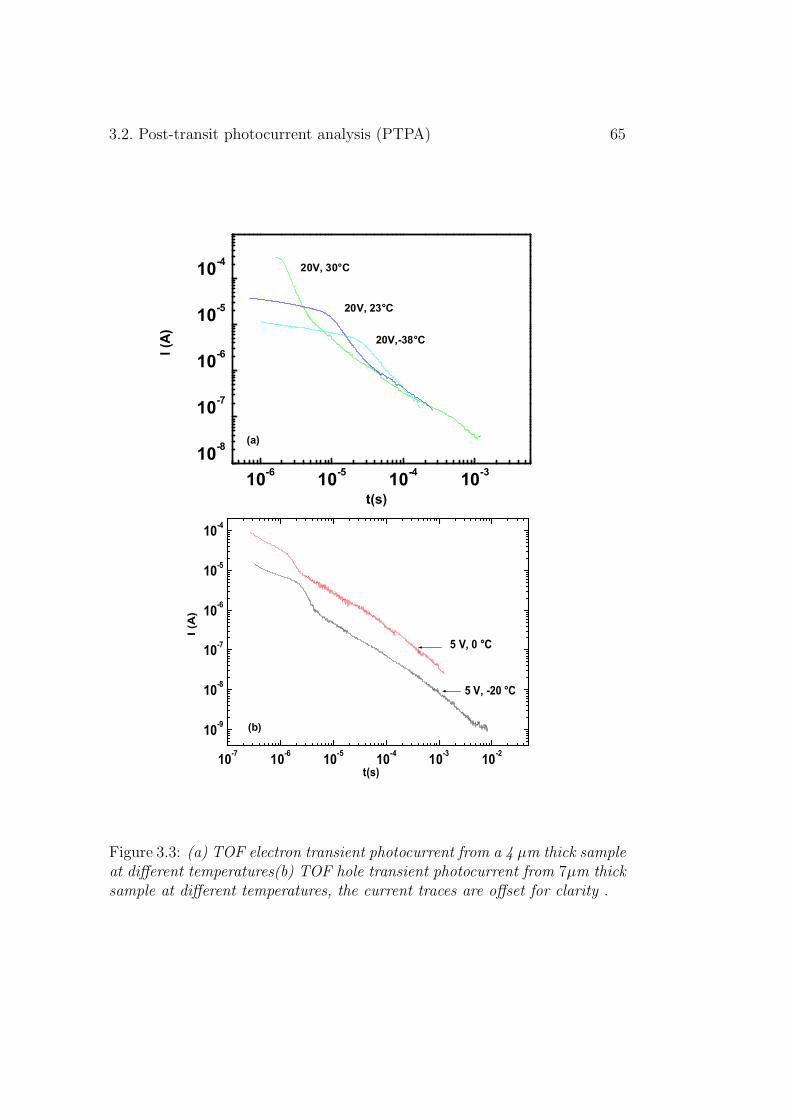
3.2. Post-transit photocurrent analysis (PTPA) 65
Figure 3.3: (a) TOF electron transient photocurrent from a 4 µm thick sampleat different temperatures(b) TOF hole transient photocurrent from 7µm thicksample at different temperatures, the current traces are offset for clarity .
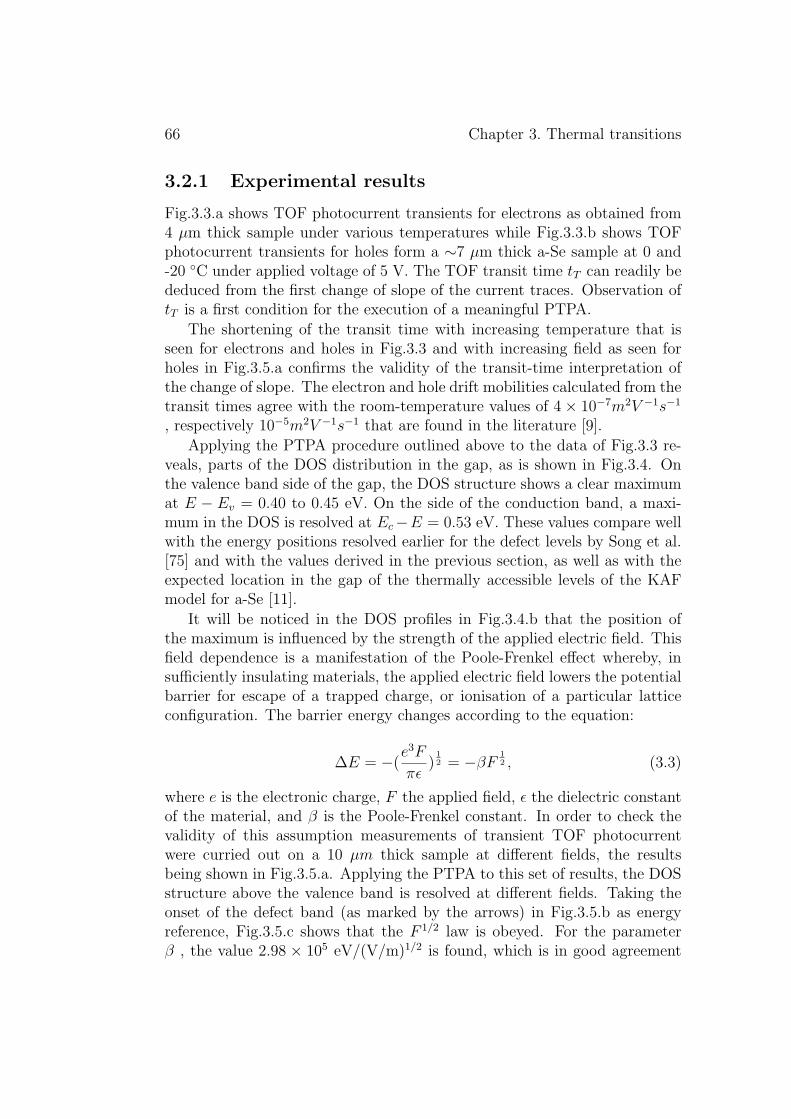
66 Chapter 3. Thermal transitions
3.2.1 Experimental results
Fig.3.3.a shows TOF photocurrent transients for electrons as obtained from4 µm thick sample under various temperatures while Fig.3.3.b shows TOFphotocurrent transients for holes form a ∼7 µm thick a-Se sample at 0 and-20 C under applied voltage of 5 V. The TOF transit time tT can readily bededuced from the first change of slope of the current traces. Observation oftT is a first condition for the execution of a meaningful PTPA.
The shortening of the transit time with increasing temperature that isseen for electrons and holes in Fig.3.3 and with increasing field as seen forholes in Fig.3.5.a confirms the validity of the transit-time interpretation ofthe change of slope. The electron and hole drift mobilities calculated from thetransit times agree with the room-temperature values of 4× 10⁻⁷m2V −1s−1
, respectively 10−5m2V −1s−1 that are found in the literature [9].
Applying the PTPA procedure outlined above to the data of Fig.3.3 re-veals, parts of the DOS distribution in the gap, as is shown in Fig.3.4. Onthe valence band side of the gap, the DOS structure shows a clear maximumat E − Ev = 0.40 to 0.45 eV. On the side of the conduction band, a maxi-mum in the DOS is resolved at Ec−E = 0.53 eV. These values compare wellwith the energy positions resolved earlier for the defect levels by Song et al.[75] and with the values derived in the previous section, as well as with theexpected location in the gap of the thermally accessible levels of the KAFmodel for a-Se [11].
It will be noticed in the DOS profiles in Fig.3.4.b that the position ofthe maximum is influenced by the strength of the applied electric field. Thisfield dependence is a manifestation of the Poole-Frenkel effect whereby, insufficiently insulating materials, the applied electric field lowers the potentialbarrier for escape of a trapped charge, or ionisation of a particular latticeconfiguration. The barrier energy changes according to the equation:
∆E = −(e3F
πε)
12 = −βF
12 , (3.3)
where e is the electronic charge, F the applied field, ε the dielectric constantof the material, and β is the Poole-Frenkel constant. In order to check thevalidity of this assumption measurements of transient TOF photocurrentwere curried out on a 10 µm thick sample at different fields, the resultsbeing shown in Fig.3.5.a. Applying the PTPA to this set of results, the DOSstructure above the valence band is resolved at different fields. Taking theonset of the defect band (as marked by the arrows) in Fig.3.5.b as energyreference, Fig.3.5.c shows that the F 1/2 law is obeyed. For the parameterβ , the value 2.98 × 10⁵ eV/(V/m)1/2 is found, which is in good agreement
3.2. Post-transit photocurrent analysis (PTPA) 67
Figure 3.4: Distribution of gap states deduced from post-transit TOF signalsfrom the samples also used in Fig.3.3 for an attempt-to-escape frequency ofν = 1012 s−1 and g(0) = 5 × 10²¹ (a) valence band side, Q0 = 7 × 10⁻¹¹C,(b) conduction band side, Q0 = 5× 10⁻¹⁰C.
68 Chapter 3. Thermal transitions
with the theoretical value of 2.84×10⁵ eV/(V/m)1/2 [9][76]. The onset of thedefect band was used instead the maximum of the feature itself because theformer is more precise as it can be easily seen. Fig.3.5.d, showing the darkcurrent in function of F 1/2 for a 28 µm thick a-Se film, further illustrates thattransport in a-Se is subject to the Poole-Frenkel effect for the field range usedin these experiments. Here, the deduced value of the Pool-Frenkel constantβ is 2.6× 10⁵ eV/(V/m)1/2.
3.2.2 Discussion
The features that appear at 0.42 eV above the valence band edge for holes,and at 0.53 eV below the conduction band edge for electrons (Fig.3.4), canbe interpreted as the emission from the occupied states of the negative-Umodel, i.e. the C0
3 and C01 that correspond to the occupied defects C+
3 and C−1
respectively. These two energetic positions do agree well with the predictionsof the negative-U model [11],[25], and the values deduced from SSPC for theT+ and T− levels in the earlier section. The above values for the energypositions of the defects are calculated with the assumption that the attempt-to-escape frequency equals 1012 s−1; a variation of this value by one order ofmagnitude, which is a possible variation for this parameter, will change theenergetic position of the features in the DOS, according kT ln(νt), by some0.05 eV at room temperature. This uncertainty introduced by the assumedvalue of ν will have to be kept in mind when looking at the energy positionsof defects.
Further support for the validity of the negative-U model for a-Se is offeredby the observed Poole-Frenkel effect on the TOF emission currents. Indeed,the fact that the field-dependent lowering of the Coulombic barrier is ob-served with carrier emission indicates that the defect centers are charged inequilibrium, i.e. when unoccupied, as postulated in the negative-U model.
Model calculations
Recently Koughia et al. [42] measured TOF photocurrent transients forelectrons as a function of the applied field, and analyzed them in terms ofa multiple-trapping model in which a trial-and-error-based inverse Laplacetechnique was used to derive the DOS distribution below the conduction bandedge. The DOS distribution is determined by comparison of the shapes ofthe measured and calculated photocurrent, the DOS being step-wise adjusteduntil there is a good agreement between measured and calculated currents.The results were then further checked by means of a Monte Carlo simulation

3.2. Post-transit photocurrent analysis (PTPA) 69
Figure 3.5: (a)Time-of-flight transient photocurrent for holes from 10 µmthick sample at different fields . (b)Distribution of gap states deduced fromtransients in (a) for an attempt-to-escape frequency ν = 1012 s−1, where thearrows show the onset of the defect level. (c) Shift of the correspondingenergy of the onset in (b) as a function of F 1/2. (d) Dependence on field ofthe dark current through a 28 µm thick sample.
70 Chapter 3. Thermal transitions
of the transients. The authors concluded that the DOS distribution consistsof four elements:
• An exponential tail with a characteristic energy of 20 meV, that willbe discussed in more detail later.
• A fairly strong peak, some 0.30 eV inside the gap, that also, will bediscussed later.
• A weaker feature at 0.45 to 0.50 eV below the conduction band mobilityedge. This peak does agree, in the energetic position, with the 0.53 eVfeature resolved in this work by means of SSPC and PTPA.
• A less well defined concentration of deep states beyond 0.65 eV.
Although the position of the 0.45− 0.50 eV level is in acceptable agreementwith the result deduced above from PTPA, it differs from the latter in sig-nificant ways. Specifically: the PTPA results produce a more prominent andwider defect peak. To examine this discrepancy more closely, an independentcomparison of measured and calculated TOF signals was carried out. An ex-perimental data set covering sufficient variation in temperature and field wasmeasured on an 18 µm thick a-Se sample. The TOF data were collected overthe wide time domain that is required for the standard post-transit analysis,providing an extended current range to be fitted. Fig.3.6 shows some of theseTOF signals. Calculations based on the analytical description of the TOFtransients as formulated by Rudenko and Arkhipov were made by Emilianovaet al. [77] to generate theoretical TOF transient that can be compared withthe experimental ones.
The calculations used the DOS distribution proposed by Koughia et al.[42] and given as:
g(E) =Ne
∆Eexp(−E − Ec
∆E) +
3∑
k=1
Nk
(2πσk)12
exp(−(E − Ek)2
2σ2k
), (3.4)
where Ec is the electron mobility edge, ∆E the width of the conductionband tail, Ek and σk are the maxima and widths of the respective Gaussianpeaks, Ne and Nk are the densities of localized states in the band tail andin the Gaussian peaks, respectively. Calculation based on the Koughia′sDOS are matched to the new data set in Fig.3.6.a where it can be seenthat, while the pre-transit photocurrent can be fitted rather well with thatDOS, calculated post-transit curves especially at the higher temperaturesand longer times show significant deviations from the experimental traces.
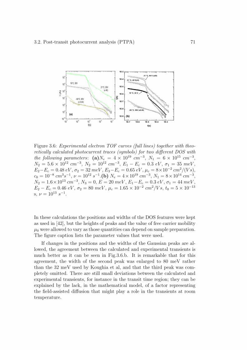
3.2. Post-transit photocurrent analysis (PTPA) 71
Figure 3.6: Experimental electron TOF curves (full lines) together with theo-retically calculated photocurrent traces (symbols) for two different DOS withthe following parameters : (a)Ne = 4 × 1019 cm−3, N1 = 6 × 1015 cm−3,N2 = 5.6 × 1012 cm−3, N2 = 1012 cm−3, E1 − Ec = 0.3 eV , σ1 = 35 meV ,E2−Ec = 0.48 eV , σ2 = 32 meV , E3−Ec = 0.65 eV , µc = 8×10⁻² cm2/(V s),c0 = 10−8 cm3s−1, ν = 1012 s−1.(b) Ne = 4×1019 cm−3, N1 = 8×1014 cm−3,N2 = 1.6×1013 cm−3, N3 = 0, E = 20 meV , E1−Ec = 0.3 eV , σ1 = 44 meV ,E2 − Ec = 0.46 eV , σ2 = 80 meV , µc = 1.65× 10⁻² cm2/V s, t0 = 5× 10⁻¹³
s, ν = 1013 s−1.
In these calculations the positions and widths of the DOS features were keptas used in [42], but the heights of peaks and the value of free carrier mobilityµ0 were allowed to vary as those quantities can depend on sample preparation.The figure caption lists the parameter values that were used.
If changes in the positions and the widths of the Gaussian peaks are al-lowed, the agreement between the calculated and experimental transients ismuch better as it can be seen in Fig.3.6.b. It is remarkable that for thisagreement, the width of the second peak was enlarged to 80 meV ratherthan the 32 meV used by Koughia et al, and that the third peak was com-pletely omitted. There are still small deviations between the calculated andexperimental transients, for instance in the transit time region; they can beexplained by the lack, in the mathematical model, of a factor representingthe field-assisted diffusion that might play a role in the transients at roomtemperature.
72 Chapter 3. Thermal transitions
Fig.3.7 shows the DOS used for fitting of the current transients togetherwith the DOS of Koughia et al.. It should be reiterated that the densities ofthe Gaussian defect peaks are sensitive to sample preparation and accidentaldoping and are therefore subject to variation from sample to sample. Thisnotion implies that the densities of Gaussian peaks are of less importancethan the widths and average energies of the peaks. While positions andwidths of the first peak are comparable in the two simulations, only theposition of the second peak is in agreement with the one in [42]; its widthturns out to be significantly broader.
It has to be noted that the time domain of the measurements reportedby Koughia et al. was restricted to just one or two decades around the tran-sit time, and that all measurements were carried out at room temperature.Based on such measurements, it is very difficult, if not impossible, to give areliable estimate for the width and exact position of a deep peak because,within this time interval, the post-transit photocurrent is still dominatedby carrier release from shallower states, and the pre-transit current cannotprovide information about either the average energy of deep states or theirdistribution.
In contrast with the results in [42], the data in this study do not indicatethe need for an additional defect density below 0.6 eV (which was enteredin the calculation, as the third peak). The obvious reason for this differencein interpretation lies in the estimated width of the second peak. The totaldensity of states in the broad second peak of this DOS model (some 1012
cm−3) does in fact match the combined density of the second peak and theadditional deep states in [42]. Within a restricted time domain around thetransit time, only the total density of deep states and not their distributioncan be estimated. To illustrate this point, it was shown that one of theexperimental TOF transients of [42] can be precisely generated on the basisof a DOS without the additional deep states, but with the 80 meV widesecond Gaussian [77].
A more recent study by Koughia and Kasap [78], using the same techniquedescribed above, claims that TOF hole transients indicate a monotonic andfeatureless distribution of states up to 0.5 eV above the valence band edge.It was further stated that adding some deep state density (about 1013 cm−3)beyond 0.5 eV leads to better results. These results are of course in totaldisagreement with the feature at 0.42 eV above EV that was resolved in thiswork by PTPA and SSPC and that will be confirmed by the TPC techniquein the next section.
For this hole TOF study, the authors measured room-temperature TOFphotocurrents at different fields, and used data taken from [79] [80] for dif-ferent temperatures. Unfortunately the common characteristic in all these

3.3. Transient photocurrent decay 73
Figure 3.7: DOS used to fit experimental TOF curves of Fig.3.6.b (full line)in comparison with DOS obtained in Koughia et al. (dotted line).
data is that they do not cover a large time domain, each of them only usingTOF traces around the transit time. This forms the key point to explain thedifference of the results. Indeed it is easier to fit transients covering smalltime ranges with an approximate DOS, than this would be the case for tran-sients covering wide time ranges such as the standard transients used in thePTPA technique. Thus, the controversy can be traced to the limited timerange used in the Koughia and Kasap experiments.
3.3 Transient photocurrent decay
As mentioned in the previous chapter, several simulation studies showed howa discrete feature on top of an exponential DOS would produce a depressionin the power-law decay of the transient photocurrent, with its position in thetime domain indicating the energetic location of the discrete trap accordingto the thermalization relation [64]. In the TPC technique both electronsand holes are participating in the current, but the more mobile carriers willdominate it. Therefore, TPC can be used to examine the valence band tail.
3.3.1 Experimental results
On a hot-pressed a-Se sample, two parallel gold contacts separated by a gapof ∼ 0.5 mm were evaporated. On this bulk gap-cell sample standard tran-sient photocurrents were measured at different temperatures, using the bluelaser flash (440 nm). A DC Voltage of 300 V was applied for these measure-ments. Fig.3.8 shows the transients. At the lower temperatures, the current
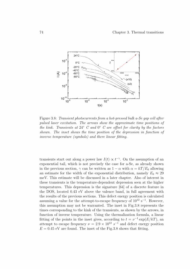
74 Chapter 3. Thermal transitions
Figure 3.8: Transient photocurrents from a hot-pressed bulk a-Se gap cell afterpulsed laser excitation. The arrows show the approximate time positions ofthe kink. Transients at 24 C and 0 C are offset for clarity by the factorsshown. The inset shows the time position of the depression in function ofinverse temperature (symbols) and there linear fitting.
transients start out along a power law I(t) ∝ t−γ. On the assumption of anexponential tail, which is not precisely the case for a-Se, as already shownin the previous section, γ can be written as 1− α with α = kT/E0 allowingan estimate for the width of the exponential distribution, namely E0 ≈ 29meV. This estimate will be discussed in a later chapter. Also of interest inthese transients is the temperature-dependent depression seen at the highertemperatures. This depression is the signature [64] of a discrete feature inthe DOS, located 0.43 eV above the valence band, in full agreement withthe results of the previous sections. This defect energy position is calculatedassuming a value for the attempt-to-escape frequency of 1012 s−1. However,this assumption may not be warranted. The inset in Fig.3.8 represents thetimes corresponding to the kink of the transients, as shown by the arrows, infunction of inverse temperature. Using the thermalization formula, a linearfitting of the points in the inset gives, according to t = ν−1 exp(E/kT ), anattempt to escape frequency ν = 2.9 × 10¹² s−1 and defect energy positionE = 0.45 eV are found. The inset of the Fig.3.8 shows that fitting.

3.4. Concluding discussion 75
3.3.2 Discussion
As can be seen in Fig.3.8, the depression in the power-law-like transientphotocurrent is thermally activated, such that at lower temperatures the kinkappears at longer times. Therefore, the use of the thermalization formula isjustified. It is unfortunate that only three points are available to determinethe value of ν. This is caused by the loss of a recognizable depression at thosetemperatures, which is probably due to recombination and dispersion at lowtemperatures. This high ν value 2.9×10¹² s−1, reflects a large trapping crosssection of the defect according to the detailed balance equation ν = N0vthσ,where N0 is the density of states at the band edge, vth a thermal velocity ofthe charge carrier and σ is the trapping cross section. This high trappingcross section is compatible with charged defects. The value 0.42 eV deducedfrom the PTPA in the previous section was calculated using ν = 1012 s−1.The newly measured value of ν puts the energy position of that defect atabout 0.45 eV . Therefore, the two techniques, PTPA and TPC, indicatethe same defect level above the valence band edge. It should be pointed outhere that the TPC measurements were done on a bulk sample which has notnecessarily the same characteristics as thin evaporated films.
3.4 Concluding discussion
Fig.3.9 is an energy diagram showing the defect levels that were deducedby the different experimental techniques described in the previous pages.Although there is a small difference in the energy position of the level T−
deduced by SSPC on one hand and PTPA and TPC on the other hand, thisis probabely due to the sensitization effect discussed in a later chapter. Agenerally good agreement is found between the positions obtained for thethermally accessible levels of the defects, T+ and T− , from SSPC, TOFand TPC measurements. This scheme for a-Se mirrors similar ones that arefamiliar from studies of the density of states of a-As2Se3.
One common feature of all experimental data sets is the asymmetric posi-tion of the defect levels with respect to the band edges; in each instance theyare shifted towards the valence band. such asymmetric shift of the negative-U energy levels towards the valence band has been reported for a-As2Se3
[28] [102], a-As2Te3 [102], a-AsSe2, a-As47Se53 [81], and a-GeSe2 [82]. Theassumption that the two-fold coordinated chalcogen sites induce a commonpreferred defect configuration in all of these compounds would explain suchgroup behavior. While a specific model for the defect configurations is avail-able for a-Se for the moment, it is not obvious how to extend it to other

76 Chapter 3. Thermal transitions
Figure 3.9: Sketch of the energy level diagram deduced for thermal transitionsT+ and T− at the negative-U co-ordination defects, on the basis of SSPC,TOF and TPC techniques.
chalcogenide compounds.The high attempt-to-escape frequency calculated from the data in Fig.3.8
means that the capture cross section of the defect is high, which is in totalagreement with the notion that the trap is charged when empty, as is charac-teristic for the charged defects in negative-U model. The high capture crosssection is also in agreement with the observed potential barrier lowering un-der applied field, i.e. the Poole-Frenkel effect, at these defects.
Since the thermally accessible levels have been resolved using severalknown techniques, the logical next step for this study would be the detec-tion of optical transitions related to the negative-U model, as indicated inFig.1.11 of the first chapter. That will be the subject of the next chapter.
Chapter 4
Optical transitions innegative-U model
Apart from the thermal transitions discussed in the previous chapter, a num-ber of purely optical transitions to and from the negative-U centers can alsobe observed. In the energy level diagram that is reproduced below as Fig.4.1,the transitions 1 and 1′ represent the absorption of an optical photon wherebyan electron is promoted from the top of the valence band to the positivelycharged defect D+ or from the negatively charged D− to the bottom of theconduction band. The charge state of the defects is of course modified inthis process. As already explained in Chapter 2, the strong electron-phononcoupling found in the chalcogenide glasses then leads to a polaronic latticedeformation around the defects sites. Consequently, while the original ab-sorption takes place at the equilibrium configuration q0 of the defect sites,all subsequent optical transitions will involve the deformed configuration qn.Such is the case for the transition 2 and 3 of Fig.4.1. Transition 2 representsphotoluminescence whereby the excited electron radiatively recombines witha hole of the valence band, while transition 3 is referred to as photoinducedabsorption since it involves excitation to the conduction band of an elec-tron whose presence at the defect site resulted itself from an earlier photonabsorption.
It is clear that experimental observation of some of these optical transi-tions in a-Se will provide further evidence for the presence of the negative-Udefects in this material. This chapter, therefore, presents and discusses theresults of three different experiments: the spectral distribution of steady-statephotoconductivity, the constant photocurrent method(CPM) and photother-mal deflection spectroscopy (PDS).
77
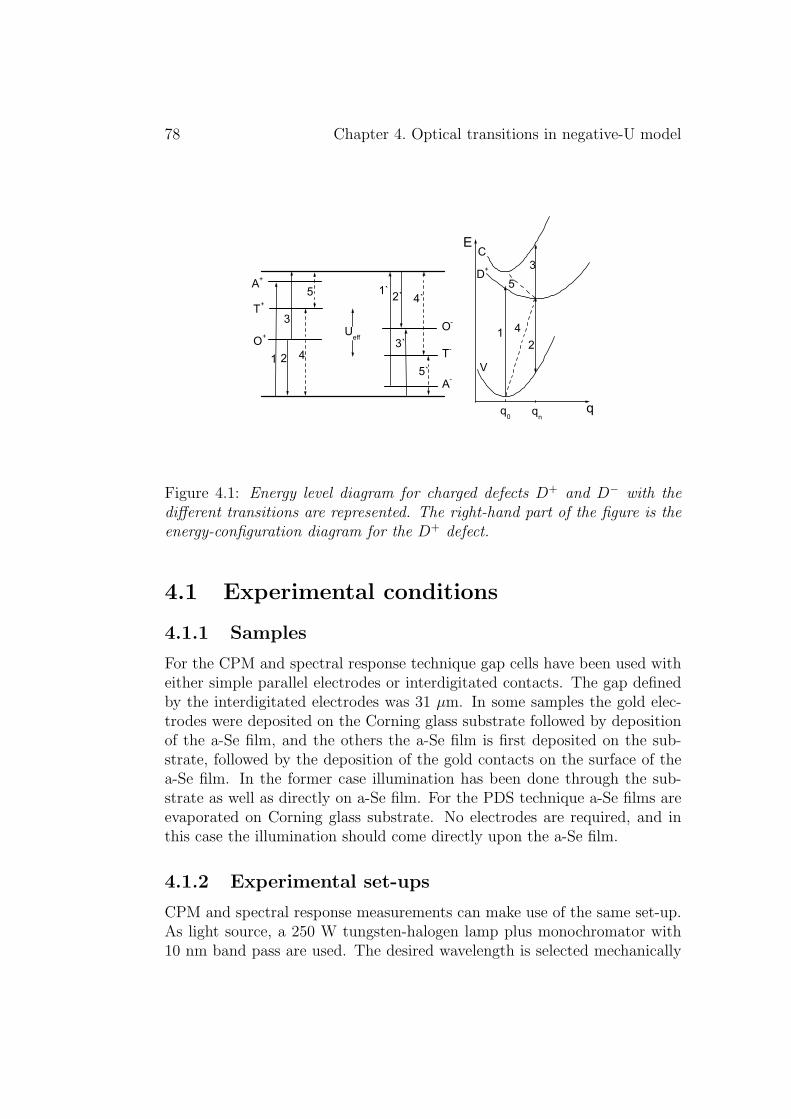
78 Chapter 4. Optical transitions in negative-U model
Figure 4.1: Energy level diagram for charged defects D+ and D− with thedifferent transitions are represented. The right-hand part of the figure is theenergy-configuration diagram for the D+ defect.
4.1 Experimental conditions
4.1.1 Samples
For the CPM and spectral response technique gap cells have been used witheither simple parallel electrodes or interdigitated contacts. The gap definedby the interdigitated electrodes was 31 µm. In some samples the gold elec-trodes were deposited on the Corning glass substrate followed by depositionof the a-Se film, and the others the a-Se film is first deposited on the sub-strate, followed by the deposition of the gold contacts on the surface of thea-Se film. In the former case illumination has been done through the sub-strate as well as directly on a-Se film. For the PDS technique a-Se films areevaporated on Corning glass substrate. No electrodes are required, and inthis case the illumination should come directly upon the a-Se film.
4.1.2 Experimental set-ups
CPM and spectral response measurements can make use of the same set-up.As light source, a 250 W tungsten-halogen lamp plus monochromator with10 nm band pass are used. The desired wavelength is selected mechanically

4.1. Experimental conditions 79
Figure 4.2: Schematic representation of the photothermal deflection spec-troscopy (transverse configuration).
with an error of less than 2 nm. A p-i-n photodiode and lock-in amplifierare used to measure the light intensity. The current is measured using eithera Keithley pico-amperemeter or a Keithley current amplifier and a milivolt-meter. A DC power supply is used to bias the sample during measurements.The sample is placed on a metal support in a vacuum chamber, where itstemperature can be controlled using a combination of liquid-nitrogen cool-ing and regulated electrical heating. As a result of the slow stabilization ofthe photocurrent, the light intensity required to keep the photocurrent at acertain constant level needs to be adjusted manually.
PDS is an optical technique where, as mentioned earlier, an electrodelesssample is used. This technique is based on the measurement of the thermalenergy released following light absorption. The sample is submerged in atransparent deflection medium (CCl4) whose index of refraction is temper-ature dependent. As the sample is irradiated by monochromatic light, themedium will be heated. As shown schematically in Fig.4.2, this causes thedeflection of the laser beam parallel to the sample surface. The deflectionis proportional to the absorption coefficient of the material. Measurementsusing this technique were carried out at the Institut for Materials Research(IMO) in Diepenbeek.
As absolute values are not needed in this study, no calibration of theCPM and PDS data is required.
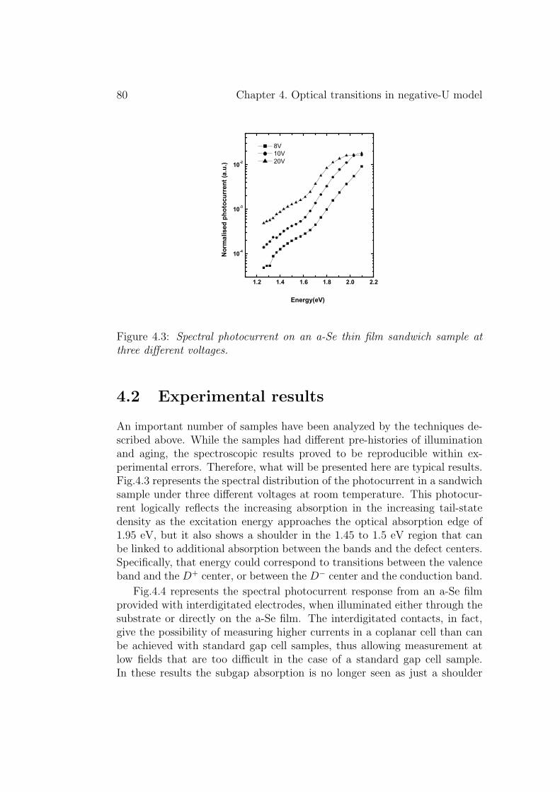
80 Chapter 4. Optical transitions in negative-U model
Figure 4.3: Spectral photocurrent on an a-Se thin film sandwich sample atthree different voltages.
4.2 Experimental results
An important number of samples have been analyzed by the techniques de-scribed above. While the samples had different pre-histories of illuminationand aging, the spectroscopic results proved to be reproducible within ex-perimental errors. Therefore, what will be presented here are typical results.Fig.4.3 represents the spectral distribution of the photocurrent in a sandwichsample under three different voltages at room temperature. This photocur-rent logically reflects the increasing absorption in the increasing tail-statedensity as the excitation energy approaches the optical absorption edge of1.95 eV, but it also shows a shoulder in the 1.45 to 1.5 eV region that canbe linked to additional absorption between the bands and the defect centers.Specifically, that energy could correspond to transitions between the valenceband and the D+ center, or between the D− center and the conduction band.
Fig.4.4 represents the spectral photocurrent response from an a-Se filmprovided with interdigitated electrodes, when illuminated either through thesubstrate or directly on the a-Se film. The interdigitated contacts, in fact,give the possibility of measuring higher currents in a coplanar cell than canbe achieved with standard gap cell samples, thus allowing measurement atlow fields that are too difficult in the case of a standard gap cell sample.In these results the subgap absorption is no longer seen as just a shoulder
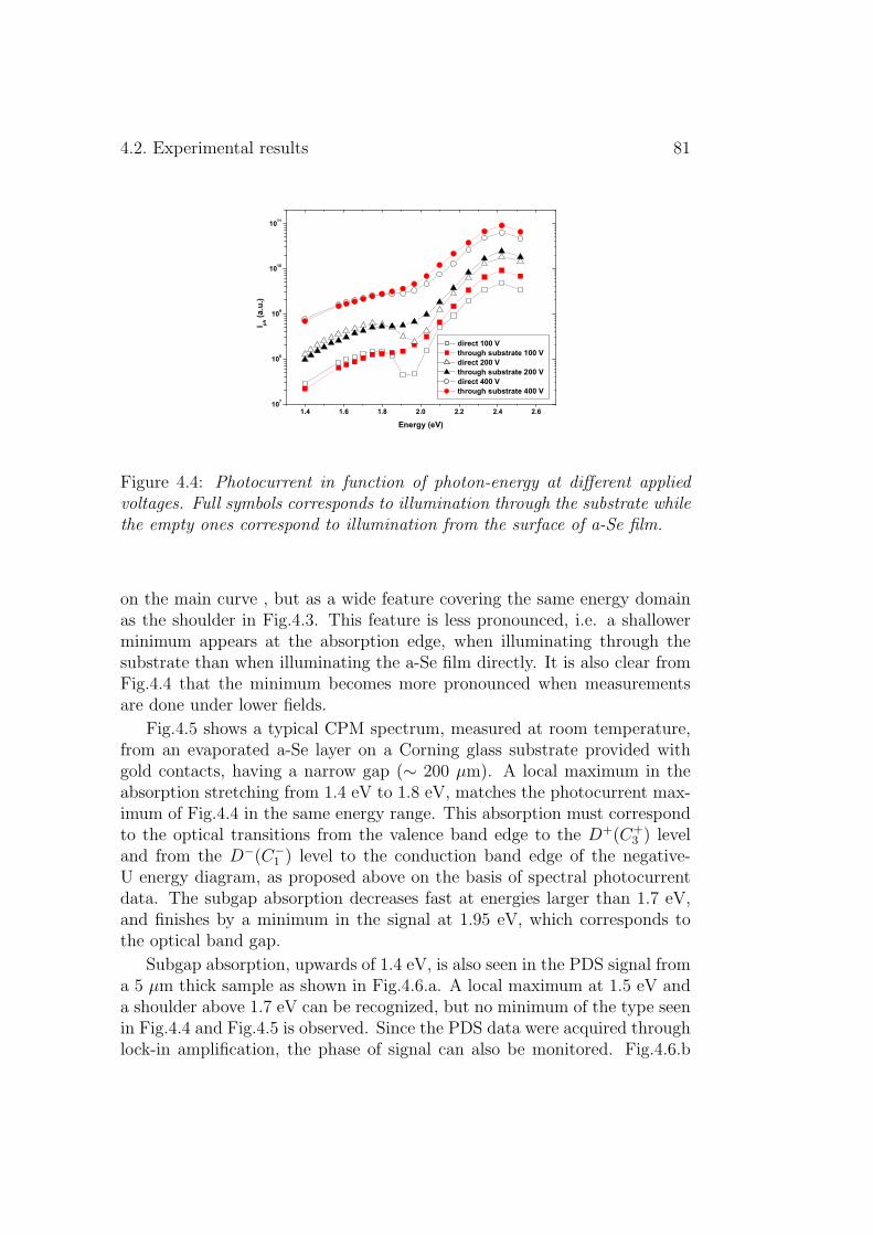
4.2. Experimental results 81
Figure 4.4: Photocurrent in function of photon-energy at different appliedvoltages. Full symbols corresponds to illumination through the substrate whilethe empty ones correspond to illumination from the surface of a-Se film.
on the main curve , but as a wide feature covering the same energy domainas the shoulder in Fig.4.3. This feature is less pronounced, i.e. a shallowerminimum appears at the absorption edge, when illuminating through thesubstrate than when illuminating the a-Se film directly. It is also clear fromFig.4.4 that the minimum becomes more pronounced when measurementsare done under lower fields.
Fig.4.5 shows a typical CPM spectrum, measured at room temperature,from an evaporated a-Se layer on a Corning glass substrate provided withgold contacts, having a narrow gap (∼ 200 µm). A local maximum in theabsorption stretching from 1.4 eV to 1.8 eV, matches the photocurrent max-imum of Fig.4.4 in the same energy range. This absorption must correspondto the optical transitions from the valence band edge to the D+(C+
3 ) leveland from the D−(C−
1 ) level to the conduction band edge of the negative-U energy diagram, as proposed above on the basis of spectral photocurrentdata. The subgap absorption decreases fast at energies larger than 1.7 eV,and finishes by a minimum in the signal at 1.95 eV, which corresponds tothe optical band gap.
Subgap absorption, upwards of 1.4 eV, is also seen in the PDS signal froma 5 µm thick sample as shown in Fig.4.6.a. A local maximum at 1.5 eV anda shoulder above 1.7 eV can be recognized, but no minimum of the type seenin Fig.4.4 and Fig.4.5 is observed. Since the PDS data were acquired throughlock-in amplification, the phase of signal can also be monitored. Fig.4.6.b
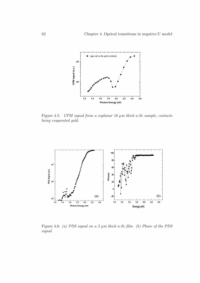
82 Chapter 4. Optical transitions in negative-U model
Figure 4.5: CPM signal from a coplanar 16 µm thick a-Se sample, contactsbeing evaporated gold.
Figure 4.6: (a) PDS signal on a 5 µm thick a-Se film. (b) Phase of the PDSsignal.

4.3. Discussion 83
Figure 4.7: CPM spectra (×, , •) for a-Se, in comparison with atransmission-based absorption spectrum (full line) and the photogenerationquantum efficiency (dotted line). The CPM data are obtained using planar-electrode samples with gap distances of 10 µm (×), 100 µm (), and 1 mm(•). (from Tanaka et al. [83]).
shows that the phase is stable at the high-energy range, but from ∼1.75 eV ondown oscillations indicate the appearance of other absorption processes. ThePDS signal is directly proportional to the a-Se optical absorption coefficientand can therefore be used to determine the optical Tauc gap of 1.95 eV, andthe slope of the exponential Urbach tail (E0 = 62 meV).
It is important to point out that in the PDS technique one deals directlywith the optical absorption while in the CPM and spectral photocurrenttechniques photoconductivity is involved. Therefore, in the former everyabsorbed photon contributes to the measured signal, while in the latter thephotogenerated electron-hole pairs have to separate before the carriers cancontribute to the photocurrent and hence be included in the measured signal.
4.3 Discussion
The three techniques do agree that there is marked subgap absorption in a-Se at about 1.5 eV. This absorption can find an interpretation in the opticaltransition 1 in Fig.4.1, i.e from the valence band to the D+ level at configu-

84 Chapter 4. Optical transitions in negative-U model
ration q0. The transition 1′ from A− to the conduction band requires higherenergy, since the A− level has to lie below the T− level, which makes thedistance to the band larger than 1.50 eV. Therefore, the absorption at ∼1.75eV may be interpreted as due to the 1′ transition. This higher-energy subgapabsorption may also find an explication in the non-related shallow defects,that will be discussed in the next chapter. Indeed, shallow states have beenidentified at 0.2 eV above EV and 0.3 eV below Ec. Nevertheless, the obser-vation of optical transitions that can fill the role of the 1 and 1′ transitionsof the negative-U system do provide experimental support for this model.
The absorption minimum at the band gap energy (1.95 eV) is remark-able. It is deeper with lower fields, or when illuminating from the a-Sefilm surface, i.e not directly through the contacts. This suggests that theelectron-hole pairs generated at this energy do often geminately recombinerather than participate in the photocurrent. Since high fields help to dissoci-ate the electron-hole pairs, the minimum in the measured signal is deeper atlower fields. Illuminating the sample from the a-Se film surface causes mostof the electron-hole pairs to be generated away from the region immediatelybetween the electrodes where the electric field is highest. In other words:this way of illuminating corresponds to the low-field case. The fact that suchgeminate recombination does not happen for the electron-hole pairs generatedthrough the subgap absorption provides further evidence that this absorptionis caused by optical transitions related to the negative-U model. Indeed, thepolaronic lattice deformation and energetic relaxation that accompanies elec-tron excitation to or from a negative-U center will break the link between thegenerated electron and hole and thus prevent geminate recombination. Ananalogous situation exists with respect to above-gap absorption: There, it isthe thermalization to lower-energy states that will disconnect the electronsand holes.
CPM results that show some similarity to the ones in Fig.4.5 have beenreported before by Tanaka et al. [83]. They are shown by the data points inFig.4.7. All relate to bulk a-Se samples and show a lower photoresponse nearthe optical gap energy than would be expected on the basis of the opticalabsorption coefficient (full line). No detailed analysis is given in [83], exceptfor a reference to geminate recombination and a comparison with reportedquantum efficiency values [84] that are shown by the dotted line of Fig.4.7.
Fig.4.8 shows the energy level diagram that has emerged so far with thethermal transitions and the estimates for the A+ and A− absorptions involv-ing D+ and D−. The optical transition level O+ that is also shown at 0.8 eVabove EV corresponds to the photoluminescence as measured before [85]. Asexplained earlier, this transition results from the radiative de-excitation of theoccupied D+ center and occurs at a changed site configuration as illustrated

4.3. Discussion 85
Figure 4.8: Sketch of the energy level diagram deduced for the negative-U co-ordination defects on the basis of the present study. Thermal levls T+andT−
were discussed in chapter three. A+andA− are the optical Levels. O+ levelcorresponds to the photoluminescence.
by transition 2 in Fig.4.1. The large energy shift between photoluminescenceand absorption fits the requirements of the negative-U model.
The small energy distance between the A+ and T+ and the A− and T−
levels, as deduced from the experiments described in this work, suggests thatthe D+ and D− defects have a rather flat energy surface in configurationspace; in other words, that the energy increase due to the presence of anelectron in the anti-bonding orbital [11] is roughly compensated by the pola-ronic lattice deformation energy. The larger energy distance between the O+
level and the others indicates that the potential energy surface of the valenceband has a stronger configurational dependence.
It is accepted that the quantum efficiency η is photon-energy [84] and fielddependent [86][87]. Therefore the measured CPM and spectral photocurrentdepend on η, while the PDS signal does not. A precise α measurement ona thick a-Se sample using the PDS technique could help to determine the

86 Chapter 4. Optical transitions in negative-U model
spectrum of η by combining it with the results of a CPM measurement. Theprecise α measure could also give more precise information about the subgapabsorption that is related to defect levels in the gap. However, applyingthe above procedure on the basis of the η curve from [84], cannot warrantproper values for α, since it was pointed out in [84] that these results arevery sensitive to preparation conditions.
4.4 Conclusion
Sub-bandgap optical absorption that is observed in photoconductivity andPDS spectra can be linked to optical transitions involving the negative-Ucenters. As shown in Fig.4.8, the optical transitions from A− to the conduc-tion band and from the valence band to A+ involve larger energies than thethermal ones, in agreement with the model. On the other hand, the smallenergetic distance between the A and T levels suggests that the D+ and D−
defects have only weakly curved energy profiles in configuration space.
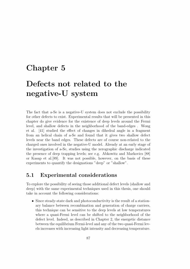
Chapter 5
Defects not related to thenegative-U system
The fact that a-Se is a negative-U system does not exclude the possibilityfor other defects to exist. Experimental results that will be presented in thischapter do give evidence for the existence of deep levels around the Fermilevel, and shallow defects in the neighborhood of the band-edges . Wonget al. [41] studied the effect of changes in dihedral angle in a fragmentfrom an helical chain of a-Se and found that it gives two shallow defectlevels near the band edges. These defects are of course non-related to thecharged ones involved in the negative-U model. Already at an early stage ofthe investigation of a-Se, studies using the xerographic discharge indicatedthe presence of deep trapping levels; see e.g. Abkowitz and Markovics [88]or Kasap et al.[89]. It was not possible, however, on the basis of theseexperiments to quantify the designations ”deep” or ”shallow”.
5.1 Experimental considerations
To explore the possibility of seeing those additional defect levels (shallow anddeep) with the same experimental techniques used in this thesis, one shouldtake in account the following considerations:
• Since steady-state dark and photoconductivity is the result of a station-ary balance between recombination and generation of charge carriers,this technique can be sensitive to the deep levels at low temperatureswhere a quasi-Fermi level can be shifted to the neighborhood of thedefect level. Indeed, as described in Chapter 2, the energetic distancebetween the equilibrium Fermi-level and any of the two quasi-Fermi lev-els increases with increasing light intensity and decreasing temperature.
87

88 Chapter 5. Defects not related to the negative-U system
Thus under a constant light intensity the position of the quasi-Fermilevel will be controlled only by temperature, and then the steady-statephotoconductivity should be sensitive to any defect band that one ofthe quasi-Fermi levels crosses in the temperature range studied. Sincethe holes are the more mobile charge carriers in a-Se, this technique willbe sensitive only to the electron traps that play a role as recombinationcenters for holes. That also the steady-state dark conductivity can besensitive to a deep level when this level is crossed by a thermally in-duced shift of the equilibrium Femi-level may be observed in Qamhiehet al. [90].
• In the time-of-flight experiment where it is possible to drift either elec-trons or holes separately, the decrease of the transient current in suc-cessive flashes may be a tool to probe the deep recombination centersfor both electrons and holes.
• The post-transit currents that were measured to determine the posi-tions of the T+ and T− levels cannot in the same way be used to locatethe shallow states. It would require very short transit times, as couldbe achieved with very thin sandwich cells. However, when one makesthe sample thinner its capacitance becomes high and the ensuing largeRC time constant will distort the transient beyond the time domain ofinterest. The alternative in this case is to use the pre-transit electroncurrent in the TOF measurements to probe possible shallow states be-low the conduction band edge, and the TPC to probe those above thevalence band edge. In both cases the accessible energies are related tothe minimum time domain that the TOF setup can measure, in practicesome 10−7 s.
5.2 Experimental results
5.2.1 Deep levels
As described in Chapter 3 the steady-state dark and photoconductivity mea-surements were performed on a-Se films using different excitation wavelengths[91]. All confirmed the typical behavior near and above room temperature,with a thermally activated dark current above 300 K and a transition fromthe monomolecular to the bimolecular recombination regime in the photocur-rent. On the other hand, below room temperature, where the observation ofan anomalous maximum in the dark conductivity was reported earlier [90],
5.2. Experimental results 89
Figure 5.1: Temperature dependence of the steady-state photocurrent for ana-Se film under 470 nm illumination for three intensities: I0 = 2 × 10¹³
photons cm−2s−1 (), 5 × 10⁻²I0 (4), and 3.8 × 10⁻³I0 (5 ). 50 V wasapplied across a 7 µm thick co-planar cell. The full symbols indicate thelevel of the dark current; (b) Dependence of the photocurrent on the lightintensity at indicated temperatures; the slopes correspond to the exponents ofthe Iph ∝ (Intensity)γ relationship.
90 Chapter 5. Defects not related to the negative-U system
an analogous maximum is now observed in the photocurrent. The open sym-bols in Fig.5.1.a show the temperature dependence of the photocurrent in ana-Se film in a log Iph versus 103/T diagram for three different light intensi-ties: I0, 5 × 10⁻²I0, and 3.8 × 10⁻³ I0, where I0 = 2 × 10¹³ photons cm−2
s−1 represents the full light intensity. At temperatures below 278 K (103/T> 3.6) the increase in the dark current (full symbols) is mirrored in the be-havior of the photocurrents. The maximum in the photocurrent intensityoccurs at somewhat higher temperatures than the one that maximizes thedark current, and the offset between those maxima increases with increasingillumination intensity.
Fig.5.1.b shows Lux-Ampere characteristics for the photocurrents inducedby 2.64 eV (470 nm) illumination at three temperatures. The chosen tem-peratures, room temperature (297 K, 103/T = 3.4), 259 K (103/T = 3.9),and 210 K (103/T = 4.8), are characteristic for the regions above, near, andbelow the low-temperature photocurrent maximum. At all temperatures thephotocurrent, Iph, grows with light intensity, and therefore photocarrier gen-eration rate G, according to Iph ∝ Gγ. Fitting these data for 297, 259, and210 K, the values of γ are 0.69 ± 0.02, 1.08 ± 0.06, and 0.88 ± 0.04 respec-tively. In other words, the photocurrent light-intensity dependence changesfrom sub-linear to super-linear and back to sub-linear as the photocurrentpasses through its low-temperature maximum.
The above results were obtained with the 2.64 eV illumination that re-sulted in the largest photocurrents. However, since the a-Se absorption depthis shallow for such photons, a follow-up set of measurements was carried outwith the more uniformly absorbed 1.96 eV light of a He-Ne laser to ascer-tain that the observed behavior is not just due to surface states. The shiftin dominant recombination regime from bimolecular to monomolecular andback to bimolecular was again observed with decreasing temperature. As willbe argued in a next section, the above observations point to photocurrentsensitization through an electron trap close to the Fermi level.
5.2.2 Shallow levels
Below conduction band edge
The pre-transit electron photocurrent is a suitable tool to probe for the pres-ence of shallow states on the conduction band side. Fig.5.2.a shows electronTOF photocurrents in a 16 µm thick a-Se sandwich cell, measured at dif-ferent temperatures between −40 C and room temperature, and with 50V applied to the sample. The abrupt change of slope of the current in the10−5 to 10−3 s region indicates the TOF transit time, with increasing tran-

5.2. Experimental results 91
Figure 5.2: (a) Electron TOF transients from a 16 µm a-Se sandwich cell atindicated temperatures and with 50 V applied. The arrows indicate the timet∗. (b) The temperature dependence of t∗.
92 Chapter 5. Defects not related to the negative-U system
sit times corresponding to decreasing temperatures as expected. A muchless pronounced change of slope can be perceived at all temperatures in thepre-transit part of the current. Arrows have been added to the figure topoint out this feature. As described in Chapter 2, the appearance of suchcusp in the photocurrent transient points to the presence of a discrete pro-truding feature in an otherwise monotonously varying density of localizedstates (DOS). A sufficiently well-defined defect and the enhanced trappinginto and subsequent release from it will cause such effect. From the tem-perature dependence of the elapsed time between the laser pulse at t = 0and the occurrence of the kink at time t∗, the energy position of the dis-crete feature with respect to the transport path can be deduced accordingto the relationship E∗ = kT ln(νt∗), where k is Boltzmann constant, T thetemperature, and ν the attempt-to-escape frequency. Fig.5.2.b shows thatthe experimentally determined t∗ is in fact thermally activated. Therefore,according to the above expression, the activation energy locates the energyposition of the defect level at E∗ = (0.28 ± 0.02) eV below the conductionband mobility edge. A value for the attempt-to-escape frequency of 4× 10¹⁰
s−1 can also be deduced for the center from the intersection of the curve withthe time axis at 1/T = 0 as can be seen in the following equation:
ln(t) = E/kT − ln(ν). (5.1)
Measurements show that the position in time of the cusp is field indepen-dent, which makes this defect center different from the charged ones involvedin the negative-U model as described in Chapter 3.
Above valence band edge
Since holes are the more mobile carriers in a-Se, the signature of a shallowtrap at the valence band side would occur in the time frame where, for thestandard sandwich cells, the true pretransit TOF signal is obscured by theRC time response of the measurement system. Therefore, TPC measure-ments on samples with interdigitated contacts offer an alternative to dealwith possible shallow states above the valence band edge. Fig.5.3.a showstransient currents in such ∼15 µm thick a-Se film deposited on Corning glassand fitted out with interdigitated gold contacts. The illumination, using bluelaser flashes, was done through the substrate, i.e. directly at the contacts.The transient currents were measured at different temperatures and for 200V applied on the sample. Similarly to the case of the pre-transit current inelectron TOF measurements, a cusp can be seen in the microsecond regionin these transients, except for the ones at room temperature and the one at0 C. The time position of this cusp vs the inverse temperature is shown in

5.2. Experimental results 93
Figure 5.3: (a) Transient photocurrent from an a-Se gap-cell sample providedwith interdigitated gold electrodes, at different temperatures. The appliedvoltage on the sample is 200 V. The arrows shows the kinks discussed in thetext. (b) The temperature dependence of the time corresponding to the firstkink. (c) The temperature dependence of the second kink.

94 Chapter 5. Defects not related to the negative-U system
Figure 5.4: Zoom in of the time frame 5 × 10⁻⁵ s to 10−2 s of the TPCcurves shown in Fig.5.3.a. The intersection between the dotted lines at anyTPC trace designates the time position of the second kink.
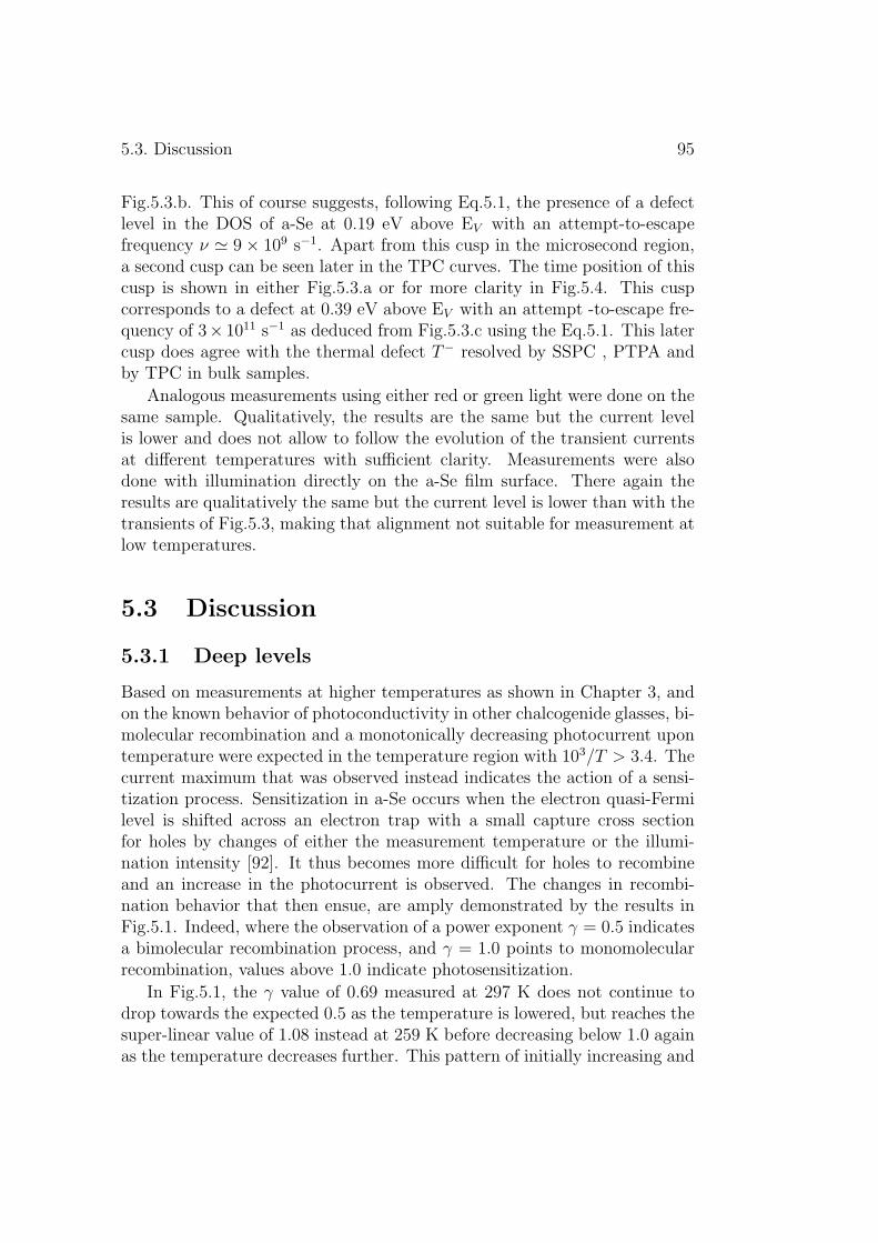
5.3. Discussion 95
Fig.5.3.b. This of course suggests, following Eq.5.1, the presence of a defectlevel in the DOS of a-Se at 0.19 eV above EV with an attempt-to-escapefrequency ν ' 9× 10⁹ s−1. Apart from this cusp in the microsecond region,a second cusp can be seen later in the TPC curves. The time position of thiscusp is shown in either Fig.5.3.a or for more clarity in Fig.5.4. This cuspcorresponds to a defect at 0.39 eV above EV with an attempt -to-escape fre-quency of 3× 10¹¹ s−1 as deduced from Fig.5.3.c using the Eq.5.1. This latercusp does agree with the thermal defect T− resolved by SSPC , PTPA andby TPC in bulk samples.
Analogous measurements using either red or green light were done on thesame sample. Qualitatively, the results are the same but the current levelis lower and does not allow to follow the evolution of the transient currentsat different temperatures with sufficient clarity. Measurements were alsodone with illumination directly on the a-Se film surface. There again theresults are qualitatively the same but the current level is lower than with thetransients of Fig.5.3, making that alignment not suitable for measurement atlow temperatures.
5.3 Discussion
5.3.1 Deep levels
Based on measurements at higher temperatures as shown in Chapter 3, andon the known behavior of photoconductivity in other chalcogenide glasses, bi-molecular recombination and a monotonically decreasing photocurrent upontemperature were expected in the temperature region with 103/T > 3.4. Thecurrent maximum that was observed instead indicates the action of a sensi-tization process. Sensitization in a-Se occurs when the electron quasi-Fermilevel is shifted across an electron trap with a small capture cross sectionfor holes by changes of either the measurement temperature or the illumi-nation intensity [92]. It thus becomes more difficult for holes to recombineand an increase in the photocurrent is observed. The changes in recombi-nation behavior that then ensue, are amply demonstrated by the results inFig.5.1. Indeed, where the observation of a power exponent γ = 0.5 indicatesa bimolecular recombination process, and γ = 1.0 points to monomolecularrecombination, values above 1.0 indicate photosensitization.
In Fig.5.1, the γ value of 0.69 measured at 297 K does not continue todrop towards the expected 0.5 as the temperature is lowered, but reaches thesuper-linear value of 1.08 instead at 259 K before decreasing below 1.0 againas the temperature decreases further. This pattern of initially increasing and
96 Chapter 5. Defects not related to the negative-U system
Figure 5.5: Temperature dependence of the power exponent γ of the Lux-Ampere characteristic measured on two pure a-Se (4 •) and one stabilized a-Se() samples.
subsequently decreasing values of γ is also seen, be it without actually ex-ceeding the 1.0 value, in Fig.5.5, which summarizes results from different a-Sesamples. That the sensitization can be observed in a-Se at low temperaturesand low illumination intensities indicates that the discrete trap level involvedmust be located close to the equilibrium Fermi level. This level of course isunrelated to the negative-U defects, because the two thermal transitions in-volved in this model have been already located in the Chapter 3 at 0.4 and0.5 eV from the valence band, respectively the conduction band edge.
The presence in a-Se of deep traps that, at room temperature, do notrelease trapped carriers for many seconds or even minutes can also be de-duced from TOF experiments. Successive measurements of the TOF signalfor either holes or electrons, under DC bias conditions [93], do show thatthe waveforms decrease in amplitude with the number of repetitions. Thephenomenon is more drastic for electrons than for holes. It suggests thatat every laser flash part of the generated charge carriers are deeply trapped,such that at the next laser flash part of the drifting charges can recombinewith the trapped ones of opposite sign. This explanation means that thereis a deep level at either side of the equilibrium Fermi-level, i.e one at the
5.3. Discussion 97
conduction band side that also causes the sensitization effect, and the secondone at the valence band side. Since electrons are the less mobile carriersin a-Se, the probability for them to recombine with trapped holes is larger,which can explain the fact that the observed phenomenon is more drastic forelectrons than holes.
While the above observations suggest the presence of deep trapping levelsin a-Se, they do not give either a precise measure for their energetic positionsor their physical origin. However, there is ample support in the literaturefor the existence of such deep levels. Most of the evidence has been basedon xerographic potential measurements [89] [94] [95] [88], but variations onthe standard TOF technique have also contributed [96] [97]. Abkowitz [8]deduced the energetic positions of these deep defects from the residual po-tential xerographic discharge. In a framework of a gap of 2.2 eV (large fora-Se), the first level is situated at 0.87 eV above the valence band edge whilethe second level lies 0.013 eV higher at the other side of the Fermi-level.These two levels were derived on the basis of an interpretation that linksthe xerographic discharge potential V at any time to a DOS that is propor-tional to dV/dt × t for E = kT ln(νt). The defect at the energy E = 0.87eV appears as a kink in the voltage decay at time greater than 83 s for anattempt-to-escape frequency of 1.4×10¹³ s−1. It is unclear how much weightshould be given to these measurements far in the decay curve, which doesnot promise much sensitivity, and given that the utilized attempt-to-escapefrequency is very high and does in practice suggest a charged defect.
In fact, the author traced these two deep levels to the T+ and T− levelsinvolved in the negative-U model. However, such assignment would not fitwell with the measured defect photoluminescence at about 0.8 eV in view ofthe accepted polaronic effects in a-Se. And it would contradict the achievedpositioning, in this work, of the T+ and T− levels at 0.5 eV below EC and0.4 eV above EV on the basis of multiple experimental data, as shown inChapter 3. In fact, the later kink in the transient photocurrents in Fig.5.3.ais a further manifestation of the T− level as shown in Fig.5.3.c. In summary:there is evidence for the existence of two deep levels, at either side of theequilibrium Fermi level, but more work is needed to clarify their physicalorigin and their precise position in the bandgap.
5.3.2 Shallow levels
The shallow electron trap, some 0.28eV below the conduction band, thatcauses the cusp in the pre-transit TOF current matches the 0.3 eV level ofthe DOS distribution that Koughia et al. [42] deduced from their study ofthe TOF transients as already described in Chapter 3. on the other hand, the

98 Chapter 5. Defects not related to the negative-U system
shallow hole trap lying at 0.2 eV above the valence band edge that is seenas the first kink in the transient photocurrents in Fig.5.3.a, has not beenexperimentally reported before. These two shallow levels represent thermaltransitions energies, but they do not match one of the thermally accessiblelevels of the negative-U model in a-Se described in Chapter 3.
It is remarkable that these two defects have a low characteristic attempt-to-escape frequency ∼ 1010 s−1 in comparison with the one for the chargeddefects that is ∼ 1012 s−1, which means, according to the detailed balanceprinciple, that they have low capture cross sections. Consequently, the shal-low defects will not be charged.
It is also remarkable that these two shallow levels more or less agree withthe energetic positions that Abkowitz [8] deduced from the drift mobilitydata in function of temperature, measured by Kasap and Juhasz [9] for bothelectrons and holes. As already pointed out elsewhere [75] as well as here inChapter 3, that assignment followed from a misinterpretation of the mobil-ity data. Indeed, the zero-field activation energy of the drift mobility (forelectrons and holes) vs the inverse temperature was interpreted as the energyposition of a trap level that controls the conduction. Marshall [69] has shownthat such interpretation of a mobility set is unwarranted.
As mentioned in Chapter 1, Lucovsky [7] introduced a model for themicrostructure of a-Se, where a-Se is constituted of long chains which lackthe regular helicity of chains in crystalline Seγ where the sign of the dihedralangle is kept constant either positive or negative. The a-Se chains contain asmall fraction of atoms that mimic the 8-atom ring structure. Thus the signof the dihedral angle can becomes random. Wong et al. [41] proposed, on thebasis of tight-binding calculations, that a distortion in the dihedral anglescan introduce pairs of shallow localized states into the gap. These statesare introduced into the gap when the lone-pair orbitals on adjacent Se arealmost in parallel alignment as in Fig.5.6.b, which is to be contrasted withthe normal bonding where these states are nearly at right angles as shownin Fig5.6.a. The shallow states are located in a range of 0.1 to 0.3 eV fromthe band edges. Therefore, the shallow states observed through the transientphotocurrents can have the distortion in dihedral angle as origin.
The pre-transit electron TOF data, as well as the TPC curves shown inFig.5.3.a have been analyzed independently (and without reference to kinkdesignations) by Marshall on the basis of a fourier transform method [98].He used the Fourier transform methods, worked by Main [99], and foundin addition to the couple of levels at EC−0.5 eV and EV +0.4 eV that arerelated to the negative-U model, two shallow levels, the first one at 0.33 eVbelow EC and the second one at 0.3 eV above EV . Representative curves ofthese results are shown in Fig.5.7. The energetic positions of the defects were
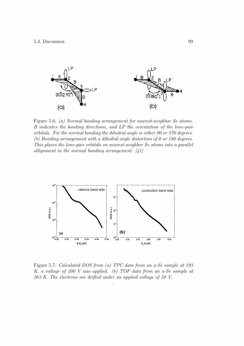
5.3. Discussion 99
Figure 5.6: (a) Normal bonding arrangement for nearest-neighbor Se atoms.B indicates the bonding directions, and LP the orientation of the lone-pairorbitals. For the normal bonding the dihedral angle is either 90 or 270 degrees.(b) Bonding arrangement with a dihedral angle distortion of 0 or 180 degrees.This places the lone-pair orbitals on nearest-neighbor Se atoms into a parallelallignment in the normal bonding arrangement. [41]
Figure 5.7: Calculated DOS from (a) TPC data from an a-Se sample at 193K, a voltage of 200 V was applied. (b) TOF data from an a-Se sample at263 K. The electrons are drifted under an applied voltage of 50 V.
.

100 Chapter 5. Defects not related to the negative-U system
deduced using E = kT ln(νt) and an attempt-to-escape frequency ν of 1012
s−1 over the full energy range. Since ν ' 1010 s−1 is more appropriate for theshallow states, this high ν value explains the somewhat larger energy valuesin the Fourier analysis. Therefore, those results are in good agreement withthe ones deduced here.
As already described in Chapter 3, the electron TOF transients shown inFig.5.2.a were also used in Emelianova et al. [77] as a reference for theoreticalcalculations of the TOF transients on the basis of the analytical descriptionof TOF by Rudenko and Arkhipov [100]. It was found that the DOS that op-timally reproduces the experimental transients does contain a shallow narrowdefect band that is situated some 0.3 eV below EC .
5.4 Conclusion
Although the defects that form the negative-U system have received mostattention in the past, a-Se does contain other defects that are not relatedto the model. Evidence for the existence of such defects has been given inthis chapter. A shallow electron trap, located at 0.28 eV below EC , and ashallow hole trap, lying at 0.19 eV above EV , make their presence knownthrough their signature in the transient photocurrent. It is more difficult,on the other hand to gain precise information on the deep traps near theFermi-level for both holes and electrons. The depth of these traps makes itdifficult to locate their energetic positions with the techniques used in thisstudy. A schematic representation of the different defect states in the a-Segap, as determined in the present work, is shown in Fig.5.8.
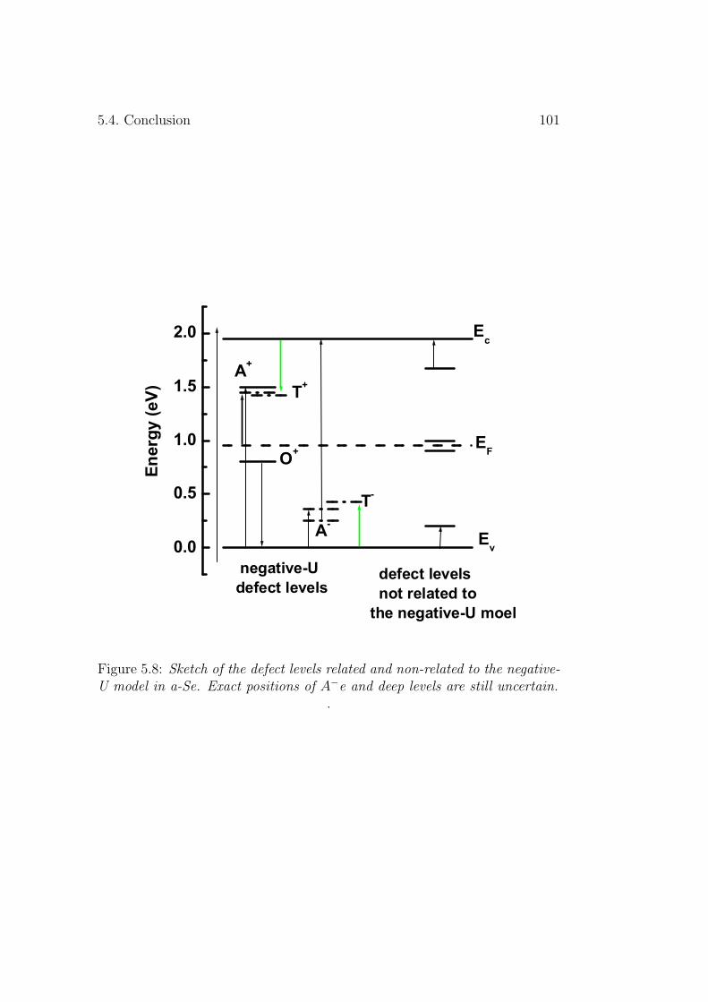
5.4. Conclusion 101
Figure 5.8: Sketch of the defect levels related and non-related to the negative-U model in a-Se. Exact positions of A−e and deep levels are still uncertain.
.
102 Chapter 5. Defects not related to the negative-U system
Chapter 6
Tail-state distributions in a-Se
The tailing and localization of electronic states caused by the topologicaldisorder in amorphous semiconductors were introduced in the first chapter.The tail-state distribution is an important part of DOS in the gap of thesemiconductors. In fact, the defect levels resolved in previous chapters aresuperposed on these tail-state distributions at the two sides of the gap. Al-though the physical origin of tail-states and coordination or configurationdefects are different, they play a similar role in determining the electronicproperties of the material. The tail-state distribution can be probed by meansof TOF and TPC measurements.
6.1 Experimental results
6.1.1 Transient photocurrent method
Transient photocurrents, together with the multiple-trapping transport model,have traditionally been used to investigate the tail-state distribution of amor-phous semiconductors. In the best-known cases such as a-As2Se3 [101] or hy-drogenated amorphous silicon (a-Si:H) [102], that distribution proved to beroughly exponential in energy and gives rise to a simple power-law behaviorof the transient current.
The results of the previous chapters have shown that it is not accurate toassume that there is an exponential tail-state distribution in a-Se, neither atthe valence band edge nor at the conduction band edge. Consequently, it isexpected that the photocurrent decay should not follow the power-law indi-cated in Chapters 2 and 3. Nevertheless, the overall shape of these photocur-rent decays at different temperatures can be used to estimate the steepnessof the average tail-state distribution at the valence band side (holes being
103
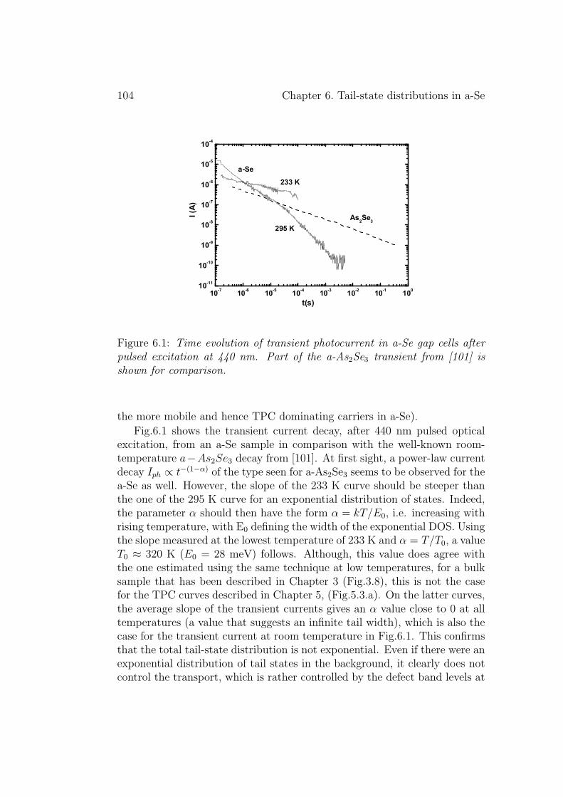
104 Chapter 6. Tail-state distributions in a-Se
Figure 6.1: Time evolution of transient photocurrent in a-Se gap cells afterpulsed excitation at 440 nm. Part of the a-As2Se3 transient from [101] isshown for comparison.
the more mobile and hence TPC dominating carriers in a-Se).
Fig.6.1 shows the transient current decay, after 440 nm pulsed opticalexcitation, from an a-Se sample in comparison with the well-known room-temperature a−As2Se3 decay from [101]. At first sight, a power-law currentdecay Iph ∝ t−(1−α) of the type seen for a-As2Se3 seems to be observed for thea-Se as well. However, the slope of the 233 K curve should be steeper thanthe one of the 295 K curve for an exponential distribution of states. Indeed,the parameter α should then have the form α = kT/E0, i.e. increasing withrising temperature, with E0 defining the width of the exponential DOS. Usingthe slope measured at the lowest temperature of 233 K and α = T/T0, a valueT0 ≈ 320 K (E0 = 28 meV) follows. Although, this value does agree withthe one estimated using the same technique at low temperatures, for a bulksample that has been described in Chapter 3 (Fig.3.8), this is not the casefor the TPC curves described in Chapter 5, (Fig.5.3.a). On the latter curves,the average slope of the transient currents gives an α value close to 0 at alltemperatures (a value that suggests an infinite tail width), which is also thecase for the transient current at room temperature in Fig.6.1. This confirmsthat the total tail-state distribution is not exponential. Even if there were anexponential distribution of tail states in the background, it clearly does notcontrol the transport, which is rather controlled by the defect band levels at
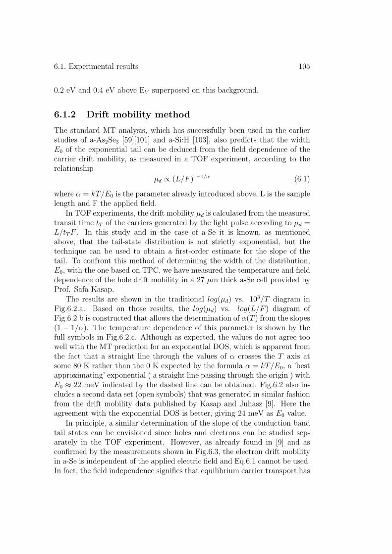
6.1. Experimental results 105
0.2 eV and 0.4 eV above EV superposed on this background.
6.1.2 Drift mobility method
The standard MT analysis, which has successfully been used in the earlierstudies of a-As2Se3 [59][101] and a-Si:H [103], also predicts that the widthE0 of the exponential tail can be deduced from the field dependence of thecarrier drift mobility, as measured in a TOF experiment, according to therelationship
µd ∝ (L/F )1−1/α (6.1)
where α = kT/E0 is the parameter already introduced above, L is the samplelength and F the applied field.
In TOF experiments, the drift mobility µd is calculated from the measuredtransit time tT of the carriers generated by the light pulse according to µd =L/tT F . In this study and in the case of a-Se it is known, as mentionedabove, that the tail-state distribution is not strictly exponential, but thetechnique can be used to obtain a first-order estimate for the slope of thetail. To confront this method of determining the width of the distribution,E0, with the one based on TPC, we have measured the temperature and fielddependence of the hole drift mobility in a 27 µm thick a-Se cell provided byProf. Safa Kasap.
The results are shown in the traditional log(µd) vs. 103/T diagram inFig.6.2.a. Based on those results, the log(µd) vs. log(L/F ) diagram ofFig.6.2.b is constructed that allows the determination of α(T ) from the slopes(1 − 1/α). The temperature dependence of this parameter is shown by thefull symbols in Fig.6.2.c. Although as expected, the values do not agree toowell with the MT prediction for an exponential DOS, which is apparent fromthe fact that a straight line through the values of α crosses the T axis atsome 80 K rather than the 0 K expected by the formula α = kT/E0, a ’bestapproximating’ exponential ( a straight line passing through the origin ) withE0 ≈ 22 meV indicated by the dashed line can be obtained. Fig.6.2 also in-cludes a second data set (open symbols) that was generated in similar fashionfrom the drift mobility data published by Kasap and Juhasz [9]. Here theagreement with the exponential DOS is better, giving 24 meV as E0 value.
In principle, a similar determination of the slope of the conduction bandtail states can be envisioned since holes and electrons can be studied sep-arately in the TOF experiment. However, as already found in [9] and asconfirmed by the measurements shown in Fig.6.3, the electron drift mobilityin a-Se is independent of the applied electric field and Eq.6.1 cannot be used.In fact, the field independence signifies that equilibrium carrier transport has

106 Chapter 6. Tail-state distributions in a-Se
Figure 6.2: (a) Hole drift mobility data set from a 27 µm thick sandwich cellwith Al bottom contact and Au top contacts; (b) drift mobility values takenfrom the fitted lines of part (a), plotted as a function of L/F; (c) full squares:temperature dependence of the parameter α as calculated from the lines inpart (b); open symbols: analogous results based on the data from [9] .

6.2. Discussion 107
Figure 6.3: Electron drift mobility in a-Se as a function of inverse tempera-ture and applied voltage. The dashed line corresponds to a 0.30 eV activationenergy.
been established before the transit time tT of the electrons. Observation ofsuch equilibrium transport rules out an exponential distribution of tail stateson the conduction band side of the gap [104]. A Gaussian, or similar steeplydecreasing DOS is needed to account for the experimental results.
6.2 Discussion
For the valence band tail states, the TOF drift mobility analysis indicatesa much steeper distribution than the exponential one observed for a-As2Se3:a width of less than 25 meV for a-Se compared to the a-As2Se3 47 meV.However, It should be pointed out that Eq.6.1 for the drift mobility andthe t−(1−α) power law for the TPC results not only presume an exponentialDOS, but are only valid for α < 1. Consequently a slope below 25 meVmeans that even room temperature may be too high to obtain a meaningfulresult. This may be the case for the 295 K on Fig.6.1, and of the curves onFig.5.3. Results that are similar to the drift mobility data set of Fig.6.2, andthe analogous one by Kasap and Juhasz, were also obtained by Marshall andOwen [76]. There the analysis leads to a 50% higher value, with E0 of theorder of 35 meV, but it should be noted that hot-pressed bulk a-Se sampleswere used rather than evaporated layers. These results are in good agreement
108 Chapter 6. Tail-state distributions in a-Se
with ones deduced from TPC traces on a bulk sample at low temperaturesFig.3.8 in Chapter 3.
calculations
The problems pointed out above do, of course, make the deduction of theslope of the tail states distribution questionable. Nevertheless, this deducedvalue of ∼25 meV is confirmed by calculations, done by Prof. Joe Marshall,on the basis of a Fourier transform of the TPC data. In fact, the results shownin Fig.5.7 can be fitted with two Gaussian defects and an underlying expo-nential tail with a 25 meV slope. (Fig.6.4 shows a similar decomposition forthe case of Fig.5.7.b). This is also in agreement with published calculations.Indeed, Naito [105] has compared a broad range of transient hole transportdata in a-Se with computer simulations based upon a trap-controlled bandtransport mechanism (multiple-trapping) for continuous distributions of lo-calized tail states. The steepness of the deduced distribution of tail stateswas calculated and found to be some 23 meV (Fig.6.5.a). A similar slope isdeduced from the calculation made by Koughia and Kasap [78] as shown inFig.6.5.b. These results of course reinforce the validity of the approach usedin this chapter to estimate the width of the tail-state distribution.
Comparable information on the a-Se conduction band tail states cannotbe procured easily through photocurrent measurements: Classical phototran-sients will only reflect the properties of the dominant carrier, which is thehole for the chalcogenides, and the TOF transients for electrons exhibit equi-librium characteristics, which necessitates a detailed fitting of the currenttransients with a complex set of analytical equations to extract an estimatefor the DOS [77][42]. For the conduction band side of the gap where the fieldindependence of the mobility precluded the application of Eq.6.1 to estimatethe distribution of tail states, Koughia et al. [42] used the TOF current tran-sients themselves as input to a numerical model for the DOS, as describedin Chapter 3. The best DOS deduced in this simulation has an exponen-tial tail-state distribution background of 20 meV in addition to the featuresdiscussed in Chapter 3.
A similar slope was found in the Emilianova et al. [77] calculations. Asmentioned in Chapter 3, whereas Koughia et al. only used the same parts ofthe TOF transients that are used to determine the transit times, and hencethe field-independent drift mobilities, Emilianova used a data set coveringa large time domain. It is acceptable, therefore, to consider this 20 meVexponential tail as one element of the DOS near the conduction band, withthe defect states described in the previous chapters being superimposed onit.

6.3. Conclusion 109
Figure 6.4: The DOS below the conduction band edge deduced by the Fouriertransform of TOF transient photocurrents from an a-Se sandwich sample(black line), together with the exponential and Gaussian compounds (opencircles) that do fit it [98].
6.3 Conclusion
The measurements and simulations do suggest that the width of the valenceand conduction band tails are comparable. The fact that both band tails arerelatively narrow clearly reduces the probability that the observation of thedefect states is hindered by a background density due to those tails, as hasbeen suggested for the case of a-As2Se3 [12].
The DOS in the gap of a-Se looks to be qualitatively symmetric, in thesense that it has comparable features on both sides of the gap and compa-rable slopes for the tails. This similarity, gives rise to the simple questionwhy the electron mobility is field-independent while the hole mobility is field-dependent. In line with the examination of such phenomenon for the case ofa-Si:H [102] [103] this difference suggests that at the transit time, transportof electrons is dominated by the trapping and release at the Gaussian distrib-uted shallow tail states, which allows a quasi-equilibrium of charge carriersbetween the transport path and those states, while this is not the case forholes where the shallow defect band is located close to the edge.
As described in Chapter 1, the top of valence band in selenium is con-stituted essentially of lone pairs orbitals while the bottom of the conduction

110 Chapter 6. Tail-state distributions in a-Se
Figure 6.5: (a) The calculated valence band states distribution by Naito et al.[105]. (b) DOS used by Koughia et al. to reproduce transient photocurrentsof holes, the inset table gives the value of mobility edge thermal shift andconcentration of deep states.
band is constituted of anti-bonding states σ∗. This undoubtedly allows tailstates at the conduction band side to have different electronic propertiesfrom those at the valence band side. Experimentally it will be worthwhile toanalyze hole and electron mobility in function of the applied field and tem-perature for samples with different thicknesses in such a way that measuredtransit times can sample a wide equivalent energy range of the tail statesdistributions.

Chapter 7
Photoinduced changes in a-Se
Up to this point, only intrinsic defects in a-Se have been dealt with, with-out the effect of external influences being considered. One of the knowneffects is the change of chalcogenides properties under illumination. Pho-toinduced changes in a variety of chalcogenide properties have of course beenstudied widely in the past [106], but very rarely have these studies includeda-Se amongst the study objects. The best-known of these effects is the pho-todarkening of the material, i.e. the narrowing of the optical gap of thechalcogenides under the influence of illumination. The darkened sample canbe bleached again by illumination with sub-gap light, or by annealing at atemperature close to the glass transition temperature. In a-Se, room tem-perature is sufficient to anneal this photodarkening, since its glass transitiontemperature is just above room temperature. In other words, photodarkeningis only stable in a-Se well below room temperature [40].
Of special interest for the defect structure of a-Se are the light-inducedelectron spin resonance (LESR) experiments that showed that a considerabledefect density could be photoinduced in chalcogenide glasses at low temper-atures, but that the defects annealed out completely at room temperature.While a-Se is only mentioned in passing in the original study of Biegelsenand Street [107], a detailed investigation of the LESR in a-Se has since beencarried out by Kolobov et al. [108]. It was reported that no measurableESR signal could be obtained at 20 K in the dark. Only by illuminating thea-Se sample with across-gap light could a signal be detected and measured.The intensity of this signal was seen to increase with illumination duration,fast at first and more slowly after some minutes, but no saturation of thephoto-induced ESR signal was observed within 2 hours of continuous illumi-nation. The ESR signal persists at low temperatures after the light is turnedoff, but annealing at 150 K makes the signal disappear. It appears that theESR signal is due to a combination of activated native defects and newly
111
112 Chapter 7. Photoinduced changes in a-Se
photoinduced ones, neither of which are stable near room temperature.Photoinduced changes in the DOS defect structure have been measured
before in chalcogenide compounds such as a-As2Se3 by, for instance, transientphotoconductivity [28] or modulated photoconductivity [109]. Those changesconsist of an increase of the defect density that is stable at room temperatureand can be annealed out at higher temperatures.
During this work, light-induced changes in the position and intensity ofthe DOS feature that is resolved from the post-transit TOF analysis wereobserved at room temperature. These observations will be presented anddiscussed in this chapter.
7.1 Experimental results
Samples of a-Se prepared for TOF measurements were illuminated over timesfrom hours to several weeks either under natural light in room ambient con-ditions or with a halogen lamp in the TOF sample holder. In the latter casethe illumination was done through a water filter as well as directly on thesample. Also the repeated use of the same sample for TOF measurementsled to the observation of photoinduced changes. Thus the results will bepresented using this division.
7.1.1 Excessively used TOF samples
Fig.7.1.a shows hole TOF transient photocurrents from a 5 µm thick a-Selayer with Al circular top contacts of 3.5 mm diameter. Curves 1 and 2 ofFig.7.1.a were measured with two different applied fields when the sample wasfresh. Curve 3 was obtained after many measurements using the same topcontact of the sample, and curve 4 shows the result of a subsequent measure-ment through a neighboring top contact that had been co-illuminated withits neighbor but without an electric field being applied. All measurementswere made at room temperature. The TOF transit time, corresponding tothe change of slope at 3 × 10⁻⁷ s, is clearly not being influenced by the re-peated measurements. Application of a lower field, as for curve 2, does resultin the anticipated lengthening of the transit time.
For post-transit currents on the other hand, it is the excessively repeatedillumination of the sample that makes a difference while the change of appliedfield has no influence. While a highly similar convex curvature is seen aroundt = 10−5s in the post-transit current of traces 1 and 2, no such curvatureis observed on curves 3 and 4 that were taken after repeated illuminationof the sample. A clearer image of the changes in the post-transit current,
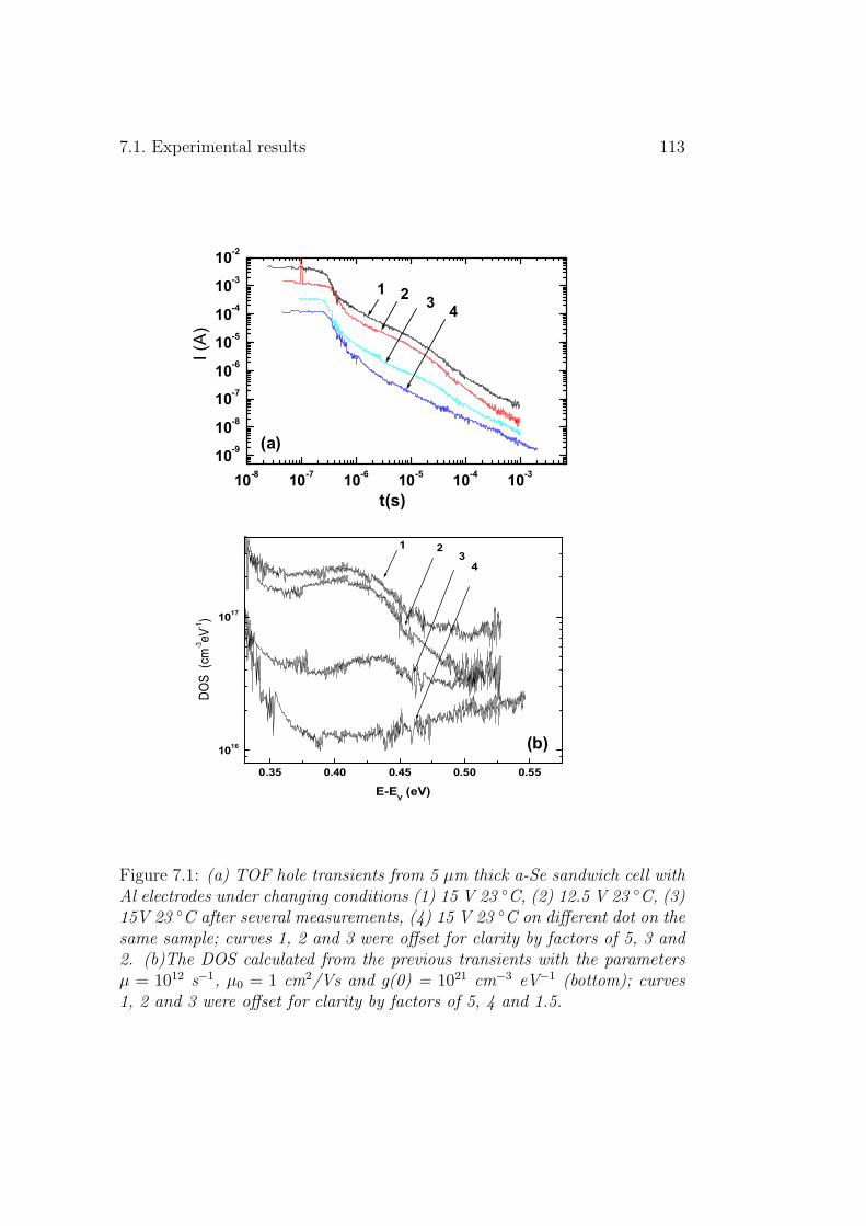
7.1. Experimental results 113
Figure 7.1: (a) TOF hole transients from 5 µm thick a-Se sandwich cell withAl electrodes under changing conditions (1) 15 V 23 C, (2) 12.5 V 23 C, (3)15V 23 C after several measurements, (4) 15 V 23 C on different dot on thesame sample; curves 1, 2 and 3 were offset for clarity by factors of 5, 3 and2. (b)The DOS calculated from the previous transients with the parametersµ = 1012 s−1, µ0 = 1 cm2/Vs and g(0) = 1021 cm−3 eV−1 (bottom); curves1, 2 and 3 were offset for clarity by factors of 5, 4 and 1.5.
114 Chapter 7. Photoinduced changes in a-Se
which is due to carrier emission from deep traps, can be obtained by extract-ing the underlying DOS using g(E) = (2g(0)/Q0t0µ)I(t)t where Q0 is thetotal charge participating in the transient photocurrent, t0 is the free-carriertransit time, and g(0) is the DOS at mobility edge. Fig.7.1.b shows theDOS distributions that correspond to the 4 curves shown in Fig.7.1.a. TheDOS maximum seen on curves 1 and 2 around 0.42 eV is in full agreementwith previously discussed results in Chapter 3. However, in curves 3 and 4this DOS structure has moved deeper in the gap. Since the shift is morepronounced with curve 4, i.e. when measured at the companion spot thatwas co-illuminated but not field-stressed, it is assumed that a photo-inducedchange in the DOS of a-Se is being seen. That change is stable at roomtemperature.
7.1.2 Samples illuminated with natural light
A twin sample to the one that led to the results described in the previousparagraphs was kept under ambient room lighting and temperature condi-tions for two weeks before being used for TOF measurements. The twosamples were co-deposited and turned into TOF samples at the same time.Hole TOF transients obtained with this second sample are shown for 2 mea-surement temperatures in Fig.7.2.a. The general behavior of the transientphotocurrent is again the one typically seen with a-Se samples, but with theemission from the deep states occurring at later times than what is normallyseen with freshly prepared samples (as described above and in Chapter 3 indetail). Fig.7.2.b again shows the DOS structure above the valence bandedge that is resolved from the current traces. A clear maximum around theenergy of 0.55 eV is seen, very reminiscent of the shift in the DOS seen withthe ”companion sample” after many TOF measurements (curve 4 of Fig.7.1).
There is one further aspect in the change in the DOS that deserves someattention. The density of states in the shifted localized level is noticeablymore pronounced against its background than is the case for the peak densityin the freshly prepared samples. The DOS rise by more than a factor of fivein Fig.7.2.b may be compared to the increase by just a factor of two forcurves 1 and 2 of Fig.7.1.b.
7.1.3 Halogen lamp illumination
An a-Se sandwich sample was prepared for TOF measurements. Hole TOFtransients were measured on this sample while it was fresh, and the resultswere just like those described above for fresh samples. Next, the sample wasilluminated using a halogen lamp. The illumination was directly onto the

7.1. Experimental results 115
Figure 7.2: (a) TOF current transients from an a-Se sandwich cell exposedto natural light and room temperature ambient conditions, and measured at23 C and 35 C. The curves are offset slightly for clarity. (b) The DOSresolved from the post-transit emission currents; the parameters listed withFig.7.1 were used for the DOS conversion.
116 Chapter 7. Photoinduced changes in a-Se
sample, i.e. no filter was used between the sample and the lamp. TOF holetransients measurements were being taken every day (the illumination wascontinuous for more than two weeks). In this condition no photoinducedchanges were detected; the TOF hole transient does duplicate itself everyday. Illumination by the halogen does increase the sample temperature bysome 10 C, i.e the sample temperature is raised to about 35 C.
The situation is not the same when illumination with the halogen lamphappens through a water filter. In this case after 24 h of illumination theDOS feature above the valence band edge shifts to 0.55 eV from the positionof 0.42 eV of either the fresh or directly illuminated sample. It was observedthat when illuminating through the water filter the sample temperature doesincrease by only 3 to 4 C.
7.1.4 Annealing effect
Photoinduced structural changes in chalcogenides do - as a rule - anneal outclose to or at the glass transition temperature. Therefore, the light-exposedsample that was discussed in section 7.1.2 was annealed at 43 C for 24 hours.Subsequently measured hole TOF photocurrents are displayed, together withthe resolved DOS curves in Fig.7.3. Comparison of the DOS after annealingwith its counterpart before annealing (Fig.7.2) reveals that, apart from asmall shift by some 0.05 eV towards the valence band edge, annealing didnot return the DOS to the initial conditions found in a freshly prepared a-Sesample. Fig.7.3 further shows that the applied electric field influences theposition of the defect peak. A field-induced shift, due to the Poole-Frenkeleffect, was observed in earlier measurements on fresh samples as describedin Chapter 3, but the magnitude of the effect is larger here.
The experimental results that are described above have been confirmedwith other sample series, prepared and measured under comparable condi-tions. Data were also collected from samples that were kept in the dark afterpreparation for times equal to the ambient exposure times of a companionsample. Such ’dark’ samples could not be distinguished from fresh samples,indicating that aging is not the cause of our observations.
7.2 Discussion
The most remarkable aspect of the photoinduced changes that were observedin the a-Se defect structure is that they are stable at room temperature,and are barely influenced by annealing at the glass transition temperature.The observation of photoinduced changes in a-Se that are stable at room

7.2. Discussion 117
Figure 7.3: (a)TOF current transients from the a-Se sandwich cell used forthe data of Fig.7.2, after annealing at the glass transition temperature for 24hours. (b) The DOS resolved from the post-transit emission currents in part(a).

118 Chapter 7. Photoinduced changes in a-Se
temperature is not evident. Up to now, observed photoinduced changes haveproven unstable at room temperature. The well-known LESR signals ofBiegelsen and Street [107] or Kolobov et al. [106] anneal out completely at150 K, just as did the photodarkening observed by Nagels at low temperatures[40]. That the effect is photo-induced follows from the observations thatprolonged exposure to the light, even in the absence of any field stressingof the sample as was the case for curve 4 in Fig.7.1 or the sample used forFig.7.2, does lead to the observed shifting of the defect peak away from thevalence band edge. Along with the changes in the energy position of the peak,its intensity with respect to the background is also changing. However, it isdifficult to ascertain whether this relative change is due to an increase of thedefect density, to a recession of the background, or to a combination of both,given that some of the constants that are needed for the DOS calculationhave to be estimated and may conceivably be subject themselves to changeunder prolonged illumination. More analysis is clearly needed to resolve thesequestions. It may be added at this point that the observation of photoinducedchanges in the defect structure that is revealed by electron rather than holetransients is more difficult, just as the observation of the DOS structure onthe conduction band side of the gap itself is more difficult. An apparent minorshift of the defects towards the conduction band is seen in some samples, buton this point as well, a more extended study is needed to clarify the results.
Possible alternative reasons for the observed effects may be examined.Since the samples are sandwich cells, it is justified to exclude humidity oroxidation as possible causes. But as the contacts have to be semi-transparentfor the TOF measurements, light soaking and aging remain as possible causes.Aging can be excluded on the basis of the experience accumulated in workingwith various a-Se samples that were intermittently used for measurements,and stored in the dark otherwise over many months, without any significantchanges in the results being observed. Crystallization of the a-Se layer canalso be excluded as cause on the basis of attempts to anneal out the photoin-duced changes: Annealing at the glass transition temperature would haveincreased the amplitude of the peak if crystallization were in play, ratherthan just shift it back a bit towards its original position as seen in Fig.7.3.Nevertheless, some reports of crystallization have appeared in the literature.Palyok et al. [110] reported that crystallization occurs in an a-Se layer whenilluminating (for some holographic recording purposes ) at room tempera-tures. They reported also that this effect is stronger above room tempera-ture. Interestingly, Reznik et al. [111] reported that grains of micro-crystals,less than 0.5 mm in diameter, appear in an a-Se layer when the film is keptin daylight at room temperature, and that this effect does not happen whenthe film temperature is about 35 C. This of course matches the experimental
7.3. Conclusion 119
observation in this work that no photoinduced changes are recorded when thesample is directly illuminated thus elevating the sample temperature to 35C. That could be explained by the fact that this temperature immediatelyanneals out the effect of light, which does not give the changes a chance toaccumulate, and thus no photoinduced changes are recorded. The macro-agglomerations seen in [111] do not explain the effect measured in this work,but the correspondence in the temperature effect leads to the deduction thatmuch smaller microcrystals than the ones reported in [111] might be thecause of the energy shift of the defect level in the gap reported above.
The parameters used to calculate the DOS might themselves play a rolein the observed shift if they should be subject to light-induced variations. In-deed, the energy scale is determined by the relationship E = kT ln(νt), whereν = 1012 s−1 has been used for all calculations. A photo-induced change ofthis parameter by two orders of magnitude would cause a room-temperatureshift of some 0.1 eV in the position of the defect peak, but the likelihood ofsuch change seems remote. As none of the above suggestions offer a goodexplanation for the observed changes in the a-Se DOS upon illumination,and as the feature that is most prominently changed has been tied to one ofthe charged coordination defects of the negative-U model, the most logicalassumption seems to be that a photoinduced change in the native negative-Udefects is being seen, possibly even involving the generation of some addi-tional centers. The set of such defects that is frozen in upon condensationof the amorphous film conceivably contains a number of them that can befurther relaxed under optical excitation, thus shifting their average energydeeper into the gap as well as increasing the peak’s prominence over thebackground by reducing the width of the distribution of defects.
7.3 Conclusion
A photoinduced shift of the T+ level has been observed in a-Se films. It shiftsnearly 0.15 eV deeper in the gap. This happens when the sample is kept innatural light in room ambient conditions, or by illuminating through a waterfilter using a halogen lamp. When illuminating by a halogen lamp withoutwater filter the sample temperature rises up to 35 C and no photo-inducedchanges are recorded. This was interpreted as due to the fact that at thistemperature the changes anneal out immediately and thus no build-up of theeffect is possible. More work is needed to elucidate the origin of this change.
120 Chapter 7. Photoinduced changes in a-Se

Summary and conclusions
This thesis deals with the electronic properties of amorphous selenium.Despite its long history as the first photoconductive semiconductor, usedfor decades in the copying machines and other applications like switchingdevices, some of its properties are still either unknown or in doubt. Forinstance: A very specific model for the negative-U centers is available for a-Se, but without experimental positioning of the defect levels in the bandgap.Additionally, it is not yet generally accepted that a-Se is a negative-U system.
The density of states model commonly used for a-Se is the Abkowitzmodel, which consists of two shallow defect levels at about 0.3 eV away fromthe valence and conduction band edges, and two deep defect levels at bothsides of the Fermi level that is roughly in the middle of the bandgap. Thesetwo pairs of defect levels are superposed on a steep tail-state distribution onboth sides of the bandgap. However, several elements of this DOS modelhave to be questioned. The activation energies of the hole and electron driftmobility were erroneously used to position the shallow defects, and the deeplevels were taken to indicate thermal transition energies in the negative-U model, even though that model itself predicts higher energies for thesetransitions. Consequently, a new and detailed study of the a-Se DOS isjustified.
To explore the DOS in a-Se, this thesis mainly used a number of steady-state and transient photoconductivity methods. It could be concluded that,effectively, a-Se is a negative-U system, and the energy level diagram for thenegative-U defects in a-Se could be constructed.
On the basis of the TOF technique and the PTPA analysis, the T− levelwas positioned at ∼0.4 eV above EV while the same level is positioned at∼0.36 eV above EV according to the SSPC technique. This difference isinterpreted to be due to a sensitization effect caused by a deep electron trapnear the Fermi level that disturbs the SSPC at low temperatures. On theother hand the T+ level, positioned at 0.53 eV below EC on the basis of thePTPA, is in good agreement with the result deduced from SSPC.
The optical levels A+ and A− were explored through the subgap opticalabsorption using the CPM and PDS techniques. The A+ was located at∼1.5 eV above EV while the A− level was located at ∼1.75 eV below EC .This puts the A+ and A− levels just beyond the corresponding T+ and T−
levels and suggests that the D+ and D− defects have only weakly curvedenergy profile in configuration space. The energetic positions of the thermaland optical levels described above agree well with the general concept of
121
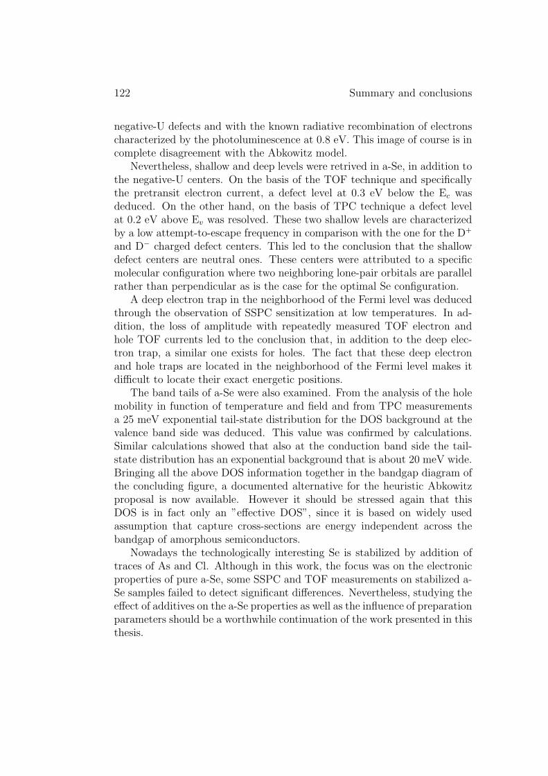
122 Summary and conclusions
negative-U defects and with the known radiative recombination of electronscharacterized by the photoluminescence at 0.8 eV. This image of course is incomplete disagreement with the Abkowitz model.
Nevertheless, shallow and deep levels were retrived in a-Se, in addition tothe negative-U centers. On the basis of the TOF technique and specificallythe pretransit electron current, a defect level at 0.3 eV below the Ec wasdeduced. On the other hand, on the basis of TPC technique a defect levelat 0.2 eV above Ev was resolved. These two shallow levels are characterizedby a low attempt-to-escape frequency in comparison with the one for the D+
and D− charged defect centers. This led to the conclusion that the shallowdefect centers are neutral ones. These centers were attributed to a specificmolecular configuration where two neighboring lone-pair orbitals are parallelrather than perpendicular as is the case for the optimal Se configuration.
A deep electron trap in the neighborhood of the Fermi level was deducedthrough the observation of SSPC sensitization at low temperatures. In ad-dition, the loss of amplitude with repeatedly measured TOF electron andhole TOF currents led to the conclusion that, in addition to the deep elec-tron trap, a similar one exists for holes. The fact that these deep electronand hole traps are located in the neighborhood of the Fermi level makes itdifficult to locate their exact energetic positions.
The band tails of a-Se were also examined. From the analysis of the holemobility in function of temperature and field and from TPC measurementsa 25 meV exponential tail-state distribution for the DOS background at thevalence band side was deduced. This value was confirmed by calculations.Similar calculations showed that also at the conduction band side the tail-state distribution has an exponential background that is about 20 meV wide.Bringing all the above DOS information together in the bandgap diagram ofthe concluding figure, a documented alternative for the heuristic Abkowitzproposal is now available. However it should be stressed again that thisDOS is in fact only an ”effective DOS”, since it is based on widely usedassumption that capture cross-sections are energy independent across thebandgap of amorphous semiconductors.
Nowadays the technologically interesting Se is stabilized by addition oftraces of As and Cl. Although in this work, the focus was on the electronicproperties of pure a-Se, some SSPC and TOF measurements on stabilized a-Se samples failed to detect significant differences. Nevertheless, studying theeffect of additives on the a-Se properties as well as the influence of preparationparameters should be a worthwhile continuation of the work presented in thisthesis.
Summary and conclusions 123
Figure : Density of states in the a-Se bandgap as deduced in this work (fullline), and as proposed by Abkowitz (dotted line). The position of the positionof the deep states can only be fixed approximately.:

124 Summary and conclusions

Bibliography
[1] W.Smith, Nature(London) 7(170) (1873) 303.
[2] J. Mort, Anatomy of Xerography (McFairland and Co., London, UK,1989).
[3] S. O. Kasap and J. A. Rowlands, in Insulating and semiconductingglasses edited by P. Boolchand (World Scientific, Singapore, 2002),p.781.
[4] S. O. Kasap and J. R. Rowlands, J. Mater. Sci. : Mater. Electron. 11(2000) 179.
[5] J. Mort, Phys. Rev. Lett. 18 (1967) 540.
[6] W. E. Spear, J. Phys. Chem. Solids 21 (1961) 110.
[7] G. Lucovsky, in The physics of selenium and tellurium, Ed by E. Ger-lach and P. Grosse, (Springer Varlag, Berlin, 1979) 210.
[8] M. Abkowitz, Phil. Mag. Lett. 58 (1988) 53.
[9] S. O. Kasap and C. Juhasz, J. Phys. D 18 (1985) 703.
[10] S. R. Elliott, Physics of amorphous materials (Longman, Essex,1990).
[11] M. Kastner, D. Adler, and H. Fritzshe, Phys. Rev. Lett. 37 (1976)1504.
[12] G. J. Adriaenssens and N. Qamhieh, J. Mater. Sci.: Mater. Electron.14 (2003) 605.
[13] D, Vanderbilt and J. D. Joannopoulos, Phys. Rev. B, 27 6311 (1983).
[14] A. Kolobov, M. Kondo, H. Oyanagi, R. Durny, A. Matsuda and K.Tanaka, Phys. Rev. B, 56 (1997) R485.
125
126 Bibliography
[15] N. F. Mott and E. A. Davis, Electronic Process in Non-CrystallineMaterials (Oxford University Press, Oxford, 1979).
[16] W.H. Zachariasen, J. Am. Chem. Soc. 54 (1932) 3841.
[17] N. F. Mott, Phil. Mag. 19 (1969) 835.
[18] D. Weaire and M. E. Thorpe, Phys. Rev. B (1971) 2508.
[19] P. W. Anderson, Phys. Rev. 109 (1958) 1492.
[20] N. F. Mott, Adv. Phys. 16 (1967) 49.
[21] M. H. Cohen, H. Fritsche and S. R. Ovshinsky, Phys. Rev. Lett. 22(1969) 1065.
[22] S. C. Agarwal, Phys. Rev. B 7 (1973) 685.
[23] S. G. Bishop, U. Strom, and P. C. Taylor, Phys. Rev. Lett. 36 (1976)543.
[24] P. W. Anderson, Phys. Rev. Lett. 34 (1975) 953.
[25] R. A. Street and N. F. Mott, Phys. Rev. Lett. 35 (1975) 1293.
[26] C. Main, and A. E. Owen, in ”Electronic and Structural Properties ofAmorphous Semiconductors”, edited by P. G. LeComber and J. Mort(Academic Press, 1973) p. 527.
[27] R. A. Street, in ”Electronic Phenomena in Non-Crystalline Semicon-ductors” (Proceeding of ICALS 6, Part A), edited by B. T. Kolomiets(Nauka,1976) p. 116.
[28] G. J. Adriaenssens, Phil. Mag. B 62, (1990) 79.
[29] K. Tanaka, J. Optoelectron. Adv. Mater. 3 (2001) 189.
[30] Mihai A. Popescu Non-Crystalline Chalcogenides (Kluwer AcademicPublishers 2000).
[31] N. Thoge, T. Minami, Y. Yamamoto and M. Tanaka, J. Appl. Phys.51 (1980) 1048.
[32] N. Thoge, H. Matsuo and T. Minami, J. Non-cryst. Solids, 89 (1987)809.
[33] D. Adler and E. J. Yoffa, Phys. Rev. Lett. 36 1197 (1976).

Bibliography 127
[34] H. Richter. J. Non-Cryst. Solids 8-10 (1972) 388.
[35] R.Kaplow. T. A. Rowe. B. L. Averbach. Phys. Rev. 168, (1968) 1068.
[36] E. A. Davis, Electronic and Structural Properties of Amorphous Semi-conductors, Eds. P. G. L. Lecomber, J. Mort, (Academic press, N. Y.London, 1973) p. 444.
[37] L. Tichy, H. Ticha, P. Nagels, E. Sleeckx and R. Callaerts, MaterialsLetters 26 (1996) 279-283.
[38] E. A. Davis, J. Non-Cryst. Solids 4 (1970) 107.
[39] B. Vanhuyse, W. Grevendonk, G. J. Adriaenssens and J. Dauwen,Phys. Rev. B 35 (1987)9298.
[40] P. Nagels, in Physics and Applications of Non-Crystalline Semiconduc-tors in Optoelectronics, Eds. A. Andriesh and M. Bertolotti, Kluwer,Dordrecht, (The Netherlands 1997) p. 109.
[41] C. K. Wong, G. Lukovsky and J. Bernholc, J. Non-Cryst. Solids 97-98(1987) 1171.
[42] K. Koughia, Z. Shakoor, S. O. Kasap and J. M. Marshall, J. Appl.Phys. 97 (2005) 033706.
[43] W. E. Spear, Proc. Phys. Soc. B 70 (1957) 669.
[44] D. Vanderbilt and J. D. Joannopoulos, Phys. Rev. B 23 (1981) 2596.
[45] S. M. Ryvkin, Photoelectric Effects in Semiconductors (New York: con-sultant Bureau, 1964).
[46] K. Weiser, R. Fischer, M. H. Brodsky, ”Proc. Tenth. Int. Conf. ofSemiconductors” (US Atomic Energy Commission, Oak Ridge, 1970)p. 667.
[47] M. Hammam, G. J. Adriaenssens and W. Grevendonk, J. Phys. C:Solid State Phys. 18 (1985) 2151.
[48] G. J. Adriaenssens, presented at the Solid State Conf., (Mansoura-Egypt, 1988).
[49] J. G. Simmons and G. W. Taylor, J. Phys. C: Solid state phys. 7 (1974)3051.
128 Bibliography
[50] M. Vacenek, J. Kocka, J. Stuchlik and A. Triska, Solid State commun.39 (1981) 1199.
[51] M. Vanecek, J. Kocka, A. Poruba ana A. Fejfar. J. Appl. Phys. 78(1995) 6203.
[52] W. E. Spear, J. Non-Cryst. Solids 1 (1969) 197.
[53] J. R, Haynes and W. Shockley, Phys. Rev. B 81 (1951) 835.
[54] M. Nesladek, F. Schauer, P. Brada, G. J. Adriaenssens and L. M. Stals,J. Non-Cryst. Solids 164-166 (1993) 505.
[55] C. E. Nebel and G. H. Bauer, J. Non-Cryst. Solids 114 (1989) 600.
[56] G. Seynhaeve, Ph.D. thesis, K. U. Leuven (1989).
[57] V. I. Arkhipov, M. S. Iovu, A. I. Rudenko and S. D. Shutov, Phys.Stat. Sol. (a) 54 (1979) 67.
[58] T. Tiedje and A. Rose, Solid St. Comm. 37 (1981) 49.
[59] J. Orenstein and M. Kastner, Phys. Rev. Lett. 46 (1981) 1421.
[60] J. M. Marshall, J. Berkin and C. Main, Phil. Mag. B 56 (1987) 641.
[61] J. M. Marshall, R. A. Street and M. J. Thompson, Phil. Mag. B 54(1986) 51.
[62] C. E. Nebel and G. H. Bauer, Phil. Mag. B 59 (1989) 463.
[63] H. Michiel, G. J. Adriaenssens and E. A. Davis, Phy. Rev. B 34 (1986)2486.
[64] J. M. Marshall and R. A. Street, Solid State Commun. 50 (1984) 91.
[65] G. Seynhaeva, G. J. Adriaenssens and H. Michiel, Solid State Commun.56 (1985) 323.
[66] M. L. Benkhedir, M. S. Aida and G. J. Adriaenssens, J. Non-Cryst.Solids 344 (2004) 193.
[67] H. Okamoto, H. Kida and Y. Hamakawa, Phil. Mag. B 49 (1984) 231.
[68] J. M. Marshall and A. E. Owen, Phil. Mag. B 24 (1971) 1281.
[69] J. M. Marshall, Phil. Mag. B 80N 9, (2000) 1705.

Bibliography 129
[70] D. Carles, G. Lefrancois and J. P. Larmagnac, J. Phys. Lett. 45 (1984)L901.
[71] J.M. Sarreau, D. Carles and C. Vautier, Thin Solid Films 7 (1971) 247.
J. P. Larmagnac, D. Carles and G. Lefrancois, J. Non-Cryst. Solids 77(1985) 1237.
[72] S. O. Kasap, Principles of Electronic Materials and Devices 2ndedn.(New York: McGraw-Hill) p 147.
[73] G. F. Seynhaeve, R. P. Barclay, G. J. Adriaenssens and J. M. Marshall,Phys. Rev. B 39 (1989) 10196.
[74] Astrid Eliat-Eliat, Ph.D Thesis, K.U.Leuven, (1997).
[75] H. -Z. Song, G. J. Adriaenssens, E. V. Emilianova and V. I. Arkhipov,Phys. Rev. B 59 (1999) 10607.
[76] J. M. Marshall, A. E. Owen, Phys. stat. Sol. (a) 12 (1972) 181.
[77] E. V. Emilianova, M. L. Benkhedir, M. Brinza and G. J. Adriaenssens,J. Appl. Phys., in press.
[78] K. Koughia and S. O. Kasap, J. Non-Cryst. Solids, in press.
[79] J. Noolandi, Phys. Rev. B 16 (1977) 4466.
[80] G. Pfister, Phys. Rev. Lett. 36 (1976) 272.
[81] G. J. Adriaenssens, Mater. Res. Soc. Symp. Proc. 61 (1986) 111.
[82] N. Qamhieh and G. J. Adriaenssens, J. Non-Cryst. Solids 292 (2001)80.
[83] K. Tanaka, S. Nakayama and N. Toyosawa, Phil. Mag. Lett. 74 (1996)281.
[84] J. C. Knights and E. A. Davis, J. Phys. Chem. Solids 35 (1974) 543.
[85] R. A. Street, T. M. Searle and I. G. Austin Phil. Mag. 29 (1974) 1157.
[86] D. M. Pai and R. C. Enck, Phys. Rev. B 11 (1975) 5163.
[87] E. V. Emilianova, N. Qamhieh, M. Brinza, G. J. Adriaenssens, S. O.Kasap, R. E. Johanson and V. I. Arkhipov, J. Non-Cryst. Solids 326, 327 (2003) 215.

130 Bibliography
[88] M. Abkowitz and J. M. Markovics, Phil. Mag. B 49 (1984) L31.
[89] S.O. Kasap, M. Baxendale, C. Juhasz, J. Appl. Phys. 62 (1987) 171.
[90] N. Qamhieh, J. Willekens, M. Brinza and G. J. Adriaenssens, J. Phys.:Condens. Matter 15 (2003) L631.
[91] N. Qamhieh, M. L. Benkhedir, M. Brinza, J. Willekens and G. J. Adri-aenssens, J. Phys.: Condens. Matter 16 (2004) 3827.
[92] A. Rose, Concepts in Photoconductivity and Allied Problems, (Krieger,Huntington, 1978).
[93] N. Qamhieh, Privat communication.
[94] M. Abkowitz and S. Maitra, J. Appl. Phys. 61 (1987) 1038.
[95] A. Kubilius, B. Petretis, V. I. Arkhipov and A. I. Rudenko, J. Non-Cryst. Solids 87 (1986) 290.
[96] S. O. Kasap, V. Aiyah, B. Polischuk and M. A. Abkowitz, Philos. Mag.Lett. 62 (1990) 377.
[97] S. O. Kasap, B. Fogal, M. Zahangir, R. E. Johanson, and S. K. O′Leary.Appl. Phys. Lett. 84 (2004) 1991.
[98] J. Marshall, privat communication.
[99] C. Main, J. Non-Cryst. Solids 299 (2002) 525.
[100] A. I. Rudenko and V .I. Arkhipov, Phil. Mag. B 45 (1982) 177.
[101] D. Monroe and M. A. Kastner, Phys. Rev. B 33 (1986) 8881.
[102] R. A. Street, Hydrogenated Amorphous Silicon, (Cambridge UniversityPress 1991).
[103] M. Brinza, E. V. Emelianova, and Guy J. Adriaenssens, Phys. Rev. B71 (2005) 115209.
[104] M. Brinza , E. V. Emelianova ,A. Stesmans and G. J. AdriaenssensMater. Res. Soc. Symp. Proc. 808(2004) A56.
[105] H. Naito, T. Iwai, T. Matsushita, and A. Sugimura, J. of Non-Cryst.solids 114 (1989) 112.

Bibliography 131
[106] A. V. Kolobov Eds. Photo-Induced Metastability in Amorphous Semi-conductors, (Wiley-VCH, Weinheim, Germany, 2003).
[107] .K. Biegelsen and R.A. Street, Phys. Rev. Lett. 44 (1980) 803.
[108] A.V. Kolobov, M. Kondo, H. Oyanagi, A. Matsuda and K. Tanaka,Phys. Rev. B 58 (1998) 12004.
[109] P. Kounavis, J. Non-Cryst. Solids 326 (2003) 98.
[110] V. Palyok, I. A. Szabo, D. L. Beke and A: Kikinneshi, Appl. Phys. A74 (2002) 683.
[111] A. Reznik, B. J. M. Lui, V. Lyubin, M. Klebanov, Y. Ohkawa, T.Matsubara, K. Miyakawa, M. Kubota, K. Tanioka, T. Kawai, J. A.Rowlands, J. Non-Cryst. Solids, in press.
132 Bibliography

Publication List
1. M. S. Aida, A. Attaf, M. L. Benkhedir
The optical properties of sputtered amorphous silicon nitride films:Effect of RF power.
Phil. Mag. B 73 (1996) 339.
2. N. Qamhieh, M. L. Benkhedir, M. Brinza, J. Willekens and G. J. Adri-aenssens
Steady-state photoconductivity in amorphous selenium glasses.
J. Phys.: Condens. Matter 16 (2004) 3827.
3. M. L. Benkhedir, M. S. Aida and G. J. Adriaenssens
Defect levels in the band gap of amorphous selenium
J. Non-Cryst. Solids 344 (2004) 193.
4. M. L. Benkhedir, M. Brinza and G. J. Adriaenssens
Electronic density of states in amorphous selenium
J. Phys.: Condens. Matter 16 (2004) S2553.
5. M. L. Benkhedir, M. S. Aida, N. Qamhieh, A. Stesmans and G. J.Adriaenssens
Experimental study of the density of states in the band gap of a-Se.
J. Optoelectron. Adv. Mater. 7 (2005) 329.
6. N. Qamhieh, M. L. Benkhedir, M. Brinza and G. J. Adriaenssens
Low-temperature steady-state photoconductivity in amorphous sele-nium films.
J. Optoelectron. Adv. Mater. 7 (2005) 1781.
7. M. L. Benkhedir, M. Brinza, J. Willekens, K. Haenen, M. Daenen, M.Nesladek and G. J. Adriaenssens
Gap-state spectroscopy in amorphous selenium.
J. Optoelectron. Adv. M. 7 (2005) 2223.
133
134 Publication List
8. A. Attaf, M. L. Benkhedir, M. S. Aida
Influence of substrate bombardment on sputtered a-Si : N thin filmproperties.
Physica B 355 (2005) 170.
9. M. Brinza, J. Willekens, M. L. Benkhedir, E. V. Emelianova and G. J.Adriaenssens
Photoconductivity methods in materials research.
J. Mater. Sci: Mater. Electron. 16 (2005) 703.
10. M. L. Benkhedir, M. Brinza, N. Qamhieh and G. J. Adriaenssens
Discrete defect levels in the amorphous selenium bandgap
J. Non-Cryst. Solids, In Press.
11. E. V. Emelianova, M. L. Benkhedir, M. Brinza and G. J. Adriaenssens
Analysis of electron time-of-flight photocurrent data from a-Se.
J. Appl. Phys. 99 (2006), in press.
12. M. Brinza, J. Willekens, M. L. Benkhedir and G. J. Adriaenssens
Photoconductivity in Materials Research,
in Handbook of Electronic and Optoelectronic Materials, Eds. S. Kasapand P. Capper (Springer, 2006) in press.