deformation and removal of semiconductor and laser single
TRANSCRIPT

International Journal of Extreme Manufacturing
TOPICAL REVIEW • OPEN ACCESS
Deformation and removal of semiconductor and laser single crystals atextremely small scalesTo cite this article: Yueqin Wu et al 2020 Int. J. Extrem. Manuf. 2 012006
View the article online for updates and enhancements.
This content was downloaded from IP address 118.123.172.211 on 25/03/2020 at 01:57
Topical Review
Deformation and removal of semiconductorand laser single crystals at extremely smallscales
Yueqin Wu1,2 , Dekui Mu2 and Han Huang1
1 School of Mechanical and Mining Engineering, The University of Queensland, QLD 4072, Australia2 Institute of Manufacturing Engineering, Huaqiao University, Xiamen, 361021, People’s Republic ofChina
E-mail: [email protected]
Received 30 December 2019, revised 11 February 2020Accepted for publication 26 February 2020Published 16 March 2020
AbstractSemiconductor and laser single crystals are usually brittle and hard, which need to be ground tohave satisfactory surface integrity and dimensional precision prior to their applications.Improvement of the surface integrity of a ground crystal can shorten the time of a subsequentpolishing process, thus reducing the manufacturing cost. The development of cost-effectivegrinding technologies for those crystals requires an in-depth understanding of their deformationand removal mechanisms. As a result, a great deal of research efforts were directed towardsstudying this topic in the past two or three decades. In this review, we aimed to summarize thedeformation and removal characteristics of representative semiconductor and laser single crystalsin accordance with the scale of mechanical loading, especially at extremely small scales. Theirremoval mechanisms were critically examined based on the evidence obtained from high-resolution TEM analyses. The relationships between machining conditions and removalbehaviors were discussed to provide a guidance for further advancing of the grindingtechnologies for those crystals.
Keywords: deformation and removal, semiconductor, laser crystal, transmission electronmicroscopy (TEM), grinding
1. Introduction
Semiconductor and laser crystals are essential substratematerials for modern electronic and photonic devices that arewidely used in communication, energy, medical, and militaryindustries. The development of advanced melt-growth meth-ods [1–5] has enabled the mass production of large-size singlecrystal ingots for semiconductors such as silicon (Si), galliumarsenide (GaAs) and gallium oxide (Ga2O3), and laser crystalssuch as yttrium aluminum garnet (YAG) and gadolinium
gallium garnet (GGG). Usually, an as-grown single crystalingot must be machined into thin substrates with high surfacequality and dimensional precision, and more importantly, freeof subsurface damage (SSD). Given the hard and brittle natureof semiconductor and laser single crystals [6], grinding iscommonly used to planarize the substrates after being slicedand achieve the required surface quality prior to further pol-ishing. An optimal balance between surface quality and pro-cessing time is the key for the success in the grinding of thosesubstrates. Therefore, the deformation and removal behaviorsof those single crystal materials were investigated extensivelyunder multiscale loading conditions. Nevertheless, the initia-tion and evolution of defects in semiconductor and lasersingle crystals induced by mechanical loading are yet to be
| IMMT International Journal of Extreme Manufacturing
Int. J. Extrem. Manuf. 2 (2020) 012006 (25pp) https://doi.org/10.1088/2631-7990/ab7a2a
Original content from this work may be used under the termsof the Creative Commons Attribution 3.0 licence. Any
further distribution of this work must maintain attribution to the author(s) andthe title of the work, journal citation and DOI.
© 2020 The Author(s). Published by IOP Publishing Ltd on behalf of the IMMT2631-8644/20/012006+25$33.00 1

thoroughly examined in a systematic manner, especially atextremely small scales.
In this review, the initiation and evolution of crystaldefects in semiconductor and laser crystals induced at extre-mely small scales were systematically summarized, and theirroles in the deformation and removal mechanisms of theselected single crystals under variable grinding conditionswere examined. The primary aim of this work is to demon-strate how the defects induced in instrumented loading atextremely small scales can be used for optimizing thegrinding processes for those single crystals. Specifically, insection 2 of this review, crystal structures, possible defectsand phase transformation, and mechanical properties oftypical semiconductor and laser single crystals are summar-ized. In section 3, we analyze the initiation of the crystaldefects in those single crystals induced by instrumentednanoindentation and nanoscratch, which are the two methodsbeing widely used to mimic the grit-work material interactionin a grinding process. In section 4, the deformation andremoval characteristics of semiconductor and laser singlecrystals involved in grinding are discussed, with an emphasison the grinding process that has extremely small materialremoval, so the deformation should occur in the ductile-likeremoval regime [7–9]. The outline of this review is schema-tically shown in figure 1, where the topics being discussed inthis work are highlighted in red.
2. Crystal structure and mechanical property
2.1. Crystal structure
Most of the semiconductor and laser single crystals areinorganic solid-state compounds, in which atoms are dis-tributed in a certain crystal structure, purely or mainly throughstrong covalent/ionic bonding [10]. The crystals thus havestable crystal structures and high melting points, hence are
‘hard’ and ‘brittle’, which are significantly different frommetals or metallic materials that exhibit more ductility undermechanical loading. Therefore, semiconductor and laser sin-gle crystals are often categorized as difficult-to-machinematerials.
Table 1 shows the crystal structures, mechanical propertiesand applications of typical semiconductor and laser single crystalmaterials, including Si, GaAs, β-Ga2O3, YAG and GGG. Thisreview focuses on these selected single crystals that haverepresentative features, and more importantly, can be grown bymelt-growth methods that have great potential to vastly reducethe cost for mass production, even though some of them arecurrently still highly priced. Among those selected materials,monocrystalline silicon is the mostly recognized first generationsemiconductors, and has been used in electronic industries fordecades and nowadays more than 95% electronics devices arefabricated on Si substrates [11]. According to [12], Si has a facecentered cubic (fcc) structure with a lattice spacing of 0.543 nm,as shown in figure 2(a) and the neighboring Si atoms are held bystrong covalent bonds, which leads to the stable crystal structureof Si. As a result, monocrystalline Si has a melting point of1410 °C, a hardness of 13GPa as measured using nanoinden-tation [6], and a fracture toughness of 0.62–1.69 MPam1/2,which is thus categorized as hard and brittle. Similar to Si, GaAsis a typical second generation semiconductor and has demon-strated superior electronic and optoelectronic properties for highfrequency applications [13]. β-Ga2O3 attracts attention for itssuperior properties owing to the incredibly large bandgap of4.7–4.9 eV [14]. Rare-earth garnet crystals, such as YAG andGGG, have been widely used in solid-state lasers and scintilla-tion detectors due to their excellent optical homogeneity andsteady chemical and physical properties [15, 16]. Note thatcrystal defects in those single crystals are often induced in theirmachining processes, even with extremely small loads and theassociated deformations involve the change of crystal structures.Therefore, high resolution transmission electron microscopy(HRTEM) must be used for the deformation characterization, as
Figure 1. Outline of this review.
2
Int. J. Extrem. Manuf. 2 (2020) 012006 Topical Review

Table 1. Crystal structure, mechanical property and applications of selected single crystals.
Selectedmaterials
Crystalstructure Unit cell
Hardness(Gpa) Toughness (MPam1/2) Crystal phases Applications References
Si Fcc a=b=c=0.5430 nm, α=β=γ=90° 13 0.62–1.29 Si-I, Si-II, Si-III,Si-XII
Electronics, photonics,solar
[6]
GaAs Fcc a=b=c=0.5650 nm, α=β=γ=90° 10.1 0.45 Zinc blende,Rocksalt
Electronics, solarenergy
[18]
β-Ga2O3 Monoclinic a=1.2214 nm, b=0.3037 nm, c=0.5798 nm,α=γ=90°, β=103.8°.
14.5 0.79 α-, β-, γ-, δ-, ε-and κ- Ga2O3
Power electronics,diode/transistor,
[19, 20]
YAG Cubic a=b=c=1.199 nm, α=β=γ=90 20.2 1.82 N.A. Laser optics [21]GGG Cubic a=b=c=1.238 nm, α=β=γ=90 13 1.2 N.A. Laser optics [22, 23]
3
Int.J.
Extrem
.Manuf.
2(2020)
012006TopicalR
eview

shown in figure 2(b), where the crystalline structure of β-Ga2O3
are clearly presented at atomic scale along the zone axis of[010] [17].
2.2. Crystal defects
Defects refer to the imperfect arrangement of atoms in asingle crystal, which might be induced during crystal growth[24–26] or by the deformation caused by mechanical loading[17, 27–29]. The defects can be briefly categorized as pointdefects (vacancy , interstitial defects, and impurities), linedefects (dislocations), planar defects (stacking faults, twin-nings, and grain boundaries), and volume defects (voids,cracks, and amorphization) [30]. Typical defects such as edgedislocation, twinning, and amorphization are illustrated infigure 3. Defects play important roles in the fabrication ofwafers and can affect the performance of final electronic andphotonic devices [31]. Usually, defects in semiconductorwafers are undesirable and may cause failures or shortenedlifetime of the fabricated electronic devices. However,initiation and evolution of defects are the prerequisite for thematerial removal in a machining process. For instance, slip-ping or cracking often leads to the chunk removal of mate-rials, and dislocations or amorphization introduced duringgrinding may facilitate the material removal in the subsequentmechanical and/or chemical polishing process. Therefore, theknowledge of initiation and evolution of the defects in
crystals is crucial for the understanding of the deformationand removal of single crystals involved in a machiningprocess.
2.3. Phase transformation
Besides the aforementioned crystal defects, the phase of an ori-ginal crystal structure may be transformed into a metastablephase that is commonly observed in semiconductor single crys-tals being deformed under mechanical loading. For example,pristine Si is of a fcc structure, but at least 13 other phases werereported at elevated pressures up to 250GPa through theoreticalcalculation or pressure cell experiments [32]. Moreover, newphases are still emerging when unconventional approaches suchas ultrafast laser-induced confined micro-explosion were suc-cessively used to handle Si crystal [33]. However, the mostcommonly reported polymorphs of Si under conventionalmechanical loading are Si-II (β-Sn, body centered tetragonal), Si-III (BC-8, body centered cubic), and Si-XII (R-8, rhombohedral)[34–36] and their crystal structures are shown in figure 4 [37].
GaAs and Ga2O3 also has different high pressure phases.Besides the most stable zinc-blende phase, GaAs has arocksalt structure [38]; while Ga2O3 has metastable structures,such as α-, γ-, δ-, ε- and κ- Ga2O3 together with the moststable β-Ga2O3 phase [19]. The knowledge of metastablephases induced upon mechanical loading is critical in theunderstanding of the metastable phase-associated deformationof semiconductor materials.
Figure 2. (a) Fcc structure of monocrystalline Si [12] and (b) HRTEM image of β-Ga2O3 [17]. (a) This crystal structure of silicon image hasbeen obtained by the author(s) from the Wikimedia website, where it is stated to have been released into the public domain. It is included inthis article on that basis. (b) Reprinted from [17] , Copyright 2017, with permission from Elsevier.
Figure 3. Typical crystal defects in semiconductor and laser crystals: (a) edge dislocation, (b) twinning and (c) amorphization. [30] 2015,reprinted by permission from the publisher (Taylor & Francis Ltd).
4
Int. J. Extrem. Manuf. 2 (2020) 012006 Topical Review

In a phase transformation, an original phase was trans-formed by breaking the original atomic bonds and subse-quently forming a new bond with the aid of applied stress. Thenewly formed phase may reserve even after stress releasing,while some transformations are reversible [39]. The char-acterization of high pressure phases is challenging since thevolume of deformation is highly localized and at nano-scale.HRTEM only examines the localized area due to the limitationof specimen preparation, but Raman spectral analysis is cap-able to cover a much larger area, which is more convenient toolto examine the occurrence of phase transformation [40–42].
3. Deformation under instrumented mechanicalloading
The deformation and removal mechanisms of single crystalsinvolved in a machining process are complicated. It is verychallenging, if not impossible, to analyze merely based on themachining parameters, because the early stage deformation ofthe machined single crystals is often concealed [43–48].Therefore, to understand the mechanisms of deformation andremoval events occurring in a grinding process, instrumentedmechanical loading using a well-shaped diamond tip or singlediamond grit is often employed to mimic the grit—workmaterial interaction involved in a fine machining process,especially at its early stage. In doing so, a thorough under-standing of the deformation and removal behaviors undermechanical loading can thus be obtained through studyinginitiation and evolution of crystal defects, and phase trans-formation of crystallite at nanometric scales, under con-trollable mechanical loads. Such instrumented mechanicalloading can be achieved through indenting, scratching andsingle grit cutting at nanometric scales. The first two methodsare the focus of this review as they are widely used and theresearch on single grit cutting is relatively limited.
3.1. Nanoindentation induced deformation
Nanoindentation was originally developed to measure thehardness and elastic modulus of a solid material or thin film atnanoscale in a non-destructive way. Later, it was utilized toinvestigate the deformation behavior of a material and its
mechanical properties can be extracted by relating the induceddeformation patterns to the applied loading conditions [17, 27,49–52]. During nanoindenting, a diamond tip is used to deforma specimen with a controlled normal load that varies from afew micro-Newtons (μN) to several tens of milli-Newtons(mN). With the aid of TEM analysis, nanoindentation makes itpossible to investigate the development of crystal defects in asingle crystal with a wide range of stress levels.
3.1.1. Deformation of Si under nanoindentation. Thedeformation of single crystal Si induced by nanoindentationhas been intensively studied [27, 34, 51, 53–59]. In thepioneering work of Wu et al [51], the deformation of singlecrystal Si under a Vickers indenter with a load of tens of mNwas systemically investigated based on the direct evidenceobtained from cross-sectional TEM examination. This studyshowed that the deformation pattern of single crystal Siincluded the formation of amorphous Si (α-Si), crystaldefects, lattice distortion, and the refinement and rotation ofgrains, but no microcracks were observed in the subsurfacezone under the Vickers indenter. More detailed knowledge onthe deformation behaviors of monocrystalline Si was obtainedby taking the effects of tip geometry and loading conditionsinto account [52, 54, 57].
Previous works [34, 60] showed that amorphization wasthe most commonly observed deformation phenomenonduring nanoindenting of monocrystalline Si and the α-Siregion was located directly beneath the indenter, i.e. aV-shaped α-Si region was observed under the Vickersindenter [51]. The crystal structures of the nanoindentationinduced α-Si were later studied by use of HRTEM andnanodiffraction to reveal the transition path for the formationof α-Si [61, 62]. The unloading rate was found to be thecontrolling factor to affect amorphous structures duringindenting of silicon [61]. The average atomic distance of α-Si varied from 0.25 to 0.28 nm when using a relatively fastunloading rate of 3 mN s−1 and ranged from 0.23 to 0.24 nmat a slower loading rate of 0.6 mN s−1 [61, 62]. This isbecause at the faster unloading rate α-Si phase wastransformed from Si-II phase; whereas at the lower unloadingrate, α-Si phase was more likely transformed from Si-XII andSi-III.
Figure 4. Crystal structures for metastable phases of (a) Si-II, (b) Si-III and (c) Si-XII. Reproduced from [37]. © IOP Publishing Ltd. Allrights reserved.
5
Int. J. Extrem. Manuf. 2 (2020) 012006 Topical Review

α-Si was firstly induced in the plastic deformation ofmonocrystalline Si during nanoindentation at relatively smallloads, or small applied stress, other crystal defects can also begenerated with increased applied stress. Zardui et al [63] useda spherical diamond tip, aimed to minimize the effect of tipshape on stress concentration, to indent a Si substrate andfound that amorphization and defects lying in {111} latticeplanes were induced and their penetration depth increasedwith the increased load. As shown in figure 5(a), similarphenomena were observed by Bradby et al [27], as stackingfaults, nanotwins and dislocation were induced in theindented monocrystalline Si at a maximum load of 80 mN[27]. Specifically, nanotwins [64] and stacking faults [51]along {111} planes were detected on the shoulder of theindent, as seen in figures 5(b) and (c), and dislocations along{111} planes were gradually penetrated into the deformedregion, as shown in figure 5(a). A single dislocation along(111) plane was generated at a relative low load of 30 mNusing a spherical tip with radius of 5 μm, and multipledislocations along both (111) and (11-1) planes wereobserved after nanoindentation at a higher applied load[63]. It is thus reasonable to derive that for the same indentershape being used a higher applied load (or stress) would leadto a greater dislocation density in monocrystalline Si.
To mimic the penetration event of a diamond gritinvolved in an ultraprecision grinding process, nanoindenta-tion was carried out at very low loads on Si surfaces. In situnanoindenting in TEM showed that at the initial stage nophase transformation occurred, but dislocations wereobserved, as shown in figure 6 [65]. It was the first timethat dislocation formation and propagation was observed in Siin situ. It is worth noting that the difference between thein situ and ex situ nanoindentation tests should be attributed tothe different confinement conditions in an ultra-thin TEMspecimen and a bulk material.
The formation of high pressure Si phases was observedwhen the indenting load was sufficiently high [27, 49, 54,56, 63, 66, 67]. Bradby et al [27] found a thin layer ofpolycrystalline material identified as rhombohedral Si-XII phaseunder a sharp and spherical tip, after the release of the load ata relatively slow unloading rate. In contrast, α-Si was formedwhen unloaded at more rapid rates. As indicated by the
cross-sectional TEM image in figure 7(a), a high pressure phaseof Si-XII was formed directly on the top surface of the indentedSi and the selected area electron diffraction (SAED) pattern infigure 7(b) was indexed as Si-XII. Zarudi et al [63] and Lloydet al [67] both reported the presence of Si-III phase on theindented Si surfaces using cross-sectional TEM analysis. Phasetransformation was also reflected on the load–displacementcurves, as crystalline nucleation at relatively low unloading rateswould lead to pop-outs on the curves, while amorphization at arelatively high unloading rate resulted in no pop-out [50].
HRTEM images enabled the direct observation of thecrystalline structures of high pressure phases [58, 68]. Thehigh resolution TEM images shown in figures 8(a)–(c) refer toSi-I, Si-III and Si-XII phases, respectively, which areconsistent with the simulated high resolution images asshown in figure 8(d) for Si-I, (e) for Si-III and (f) for Si-XII[58]. Apparently, HRTEM results provide the direct evi-dences of the existence of both Si-III and Si-XII phases. Veryrecently, a new phase transformation pathway was reported,in which a transition from Si-I to Si-VI was demonstrated byin situ TEM with atomic scale resolution [64].
The phase transformation route for single crystal Si undermechanical stress can be summarized in figure 9. In summary,the pristine Si-I phase transforms into Si-II upon appliedstress, but the formation of either α-Si or high pressure phasesis dependent on the loading and unloading conditions: whenthe applied stress is sufficiently low, only α-Si is formed afterunloading; when the applied stress is sufficiently high, α-Si isformed at high unloading rates, while high pressure phaseswill be formed at relatively low unloading rates. Moreover,nanocrystals with the same crystal structure as Si-I mightrecrystallize from α-Si.
Molecular dynamics (MD) simulation was often used tounderstand the mechanism for phase transformations inducedby nanoindentation [53, 69–73]. MD simulation enables themonitoring of positioning of Si atoms under mechanicalloading, so that the crystal structures after transformationwould be identified convincingly, such as the transformationsfrom Si-I to Si-II during loading and to Si-III, Si-XII and α-Siduring unloading. In general, the MD simulation results agreewell with the experimental results [58, 68] presented earlier.Apparently, MD can be a useful complement to TEM, which
Figure 5. (a) Bright field (BF) cross-sectional TEM image of a spherical indent on Si with a maximum load of 80 mN [27]; and HRTEMimages of induced (b) nanotwins [64] and (c) stacking faults [51]. (a) Reprinted from [27], with the permission of AIP Publishing.(b) Reproduced from [64], with permission of The Royal Society of Chemistry. (c) Reprinted from [51], Copyright 1999, with permissionfrom Elsevier Ltd. on behalf of Acta Materialia Inc. All rights reserved.
6
Int. J. Extrem. Manuf. 2 (2020) 012006 Topical Review

Figure 6. TEM images taken from a video of an in situ nanoindentation into silicon showing: (a) defect free Si sample prior to indentation,(b) and (c) the elastic strain contours at the initial indenting stages, (d) and (e) dislocations started to nucleate, (f) the residual dislocations andstrain contours after releasing the applied pressure. [65] 2005, reprinted by permission of the publisher (Taylor & Francis Ltd).
Figure 7. (a) Dark field cross-sectional TEM image of a spherical indent on Si made at a maximum load of 20 mN and (b) the SAED patternof polycrystalline region. Reprinted from [27], with the permission of AIP Publishing.
7
Int. J. Extrem. Manuf. 2 (2020) 012006 Topical Review

help understand the deformation mechanism of crystalmaterials.
3.1.2. Deformation of GaAs under nanoindentation. The factthat Ga–As atomic bonding strength in single crystal GaAs isweaker than that of Si-Si bond in Si [74, 75], together with theanisotropic properties of GaAs, makes the deformation patternof GaAs significantly different from that of Si. Thus, it isexpected that the deformation mechanism of GaAs is differentfrom that of Si. The nanoindentation studies on the deformationmechanism of GaAs were mainly focused on the (001) crystalplane [29, 38, 76–80]. Those studies used different indentersincluding Berkovich [81, 82], Vickers [18, 76, 83], andspherical diamond tips [84–86]. Pop-ins were commonlyobserved on their load–displacement curves, which should beattributed to the sudden nucleation of slips in the GaAs beingindented. The critical loads for the occurrence of pop-ins wereconsiderably affected by tip geometries [84, 87].
Prior to the nucleation of slips, dislocation was firstlyinduced in GaAs at extremely low loads (typically smaller
than 0.2 mN when using a sharp cube corner indenter),verified by TEM examination [88]. The dislocation activity inGaAs induced by nanoindentation was also investigated bymeans of MD analysis [89]. TEM was employed to examinethe deformation from both plane and cross-sectional views,and an example is shown in figure 10 [90], where TEMimaging revealed complicated dislocation arrangements in theindented GaAs including both stacking faults and perfectdislocations. The dislocations in the rosette arms werecritically investigated [81, 90–93], showing that the asymme-trical rosette was attributed to the effects of tip geometry.Moreover, the rosette arm along the [110] direction wasconstituted of perfect dislocations, and the length of rosettearm depended on the mobility of dislocations. Twin structuresoccurred in GaAs when further increased the indentation load[84, 85], which is shown in figure 11(a) with its HRTEMimage of twins in figure 11(b). The crystallographic structureof the induced twins was demonstrated to be strongly relatedto the apex angle of the indenter [94, 95]: diverging twinswere formed when the indenter apex angle is smaller than70.5° that is the angle between two {111} lattice planes ofGaAs, as shown in figure 11(a); otherwise, convergent twinswould be induced. Further increase in indentation load wouldinduce median cracks [94–96]. The formation of cracks wasattributed to the highly concentrated stress field induced bythe sharp diamond tips [97].
The phase transformation frequently observed in thedeformation of Si was not experimentally observed duringnanoindentation of GaAs, but the powderization or evenamorphization was reported, which was under the circum-stances of ultra-high pressure or extremely severe deforma-tion conditions [18]. Although MD simulation suggested thatthe phase transformation [38] from original zinc-blende torock-salt like structure would occur during nanoindetation of
Figure 8. High resolution TEM images of (a) Si-I, (b) Si-III and (c) Si-XII; (d)–(f) are their respective simulated high resolution images.Reprinted from [58], with the permission of AIP Publishing.
Figure 9. The phase transformation pattern of silicon underindentation. Si-I* refers to nanocrystals of Si-I phase.
8
Int. J. Extrem. Manuf. 2 (2020) 012006 Topical Review

GaAs, however, such transformation has never been experi-mentally verified. One of the possible explanations is becausea reverse transformation might occur during unloadingof GaAs.
The effect of n-type (Si) or p-type (Zn) doping on thedeformation of GaAs was investigated using nanoindenta-tion by Le Bourhis et al [29]. They also studied thedislocation activity by indenting along two differentorientations using a Berkovich indenter. It was found thatthe indentation rosette structure appeared to be affected bydoping and indenter orientation, but the hardness, shearstress, and critical load of pop-in event were not obviouslyinfluenced [29].
In summary, the deformation patterns of single crystalGaAs induced by nanoindentation include dislocation,twining, stacking faults, and amorphization when thedeformation is insufficient to induce micro-crack. Accordingto our literature study, no high-pressure phase was observedexperimentally.
3.1.3. Deformation of β-Ga2O3 under nanoindentation.Monocrystalline β-Ga2O3 is a newly developed and arepresentative for the third-generation semiconductormaterials. Till now, the studies of the mechanical propertiesand deformation behaviors of β-Ga2O3 are lacking [17, 98].Wu et al investigated the nanoindentation-induced deformationin β-Ga2O3 single crystal using TEM [17] and found thatstacking faults along the (200) lattice planes and twinningstructures with (2̄01) lattice plane as twin boundary were firstlyinduced, as shown in figure 12(a). HRTEM images togetherwith the corresponding electron patterns in figures 13(a) and(b) illustrated the characteristics of stacking faults and twiningstructures, respectively. Subsequent to stacking faults andtwining, dislocations started to initiate at relatively high loadson (101) lattices planes. With the further increase in indentationload, densities of stacking faults, twins and dislocationsbecame higher, forming a deeper defect layer. When theindentation load was sufficiently high (such as the case of10 mN when using a conical diamond tip with a radius of 1 μm
Figure 10. TEM plane views of the indents made at room temperature in bulk (001) GaAs at different loads of (a) 0.28 mN and (b) 3 mN. [90]John Wiley & Sons. Copyright © 2007 WILEY-VCH Verlag GmbH & Co. KGaA, Weinheim.
Figure 11. (a) Cross-sectional TEM image of the indent made using a 60° wedge tip on GaAs, obtained on the zone axis of [−110]. (b) Highmagnification TEM image of the area containing high density of divergent twins and the inset is the electron diffraction pattern of the twiningstructure. (c) HRTEM image of the twins, the white arrows point to the twin boundaries. Reprinted from [95], Copyright 2008, withpermission from Elsevier Ltd. on behalf of Acta Materialia Inc. All rights reserved.
9
Int. J. Extrem. Manuf. 2 (2020) 012006 Topical Review

[13]), crack was initiated and propagated along (200) latticeplanes (figure 12(b)) and (2̄01) lattice planes were bent(figure 12(c)).
3.1.4. Deformation of laser crystals under nanoindentation.Nanoindentation induced surface/subsurface deformation of
single crystal GGG was investigated by use of electronmicroscopic analyses [99]. Plastic flow lines were found to bedistributed hierarchically on the indented surface from SEMexamination. A typical cross-sectional TEM image of theindented GGG using a Berkovich tip with a tip radius of40 nm is presented in figure 14(a), where no subsurface
Figure 12. BF cross-sectional TEM images of deformed subsurface under indentation loads of (a) 1 and (b) 10 mN. Both TEM images weretaken on the same zone axis of [010]. (c) HRTEM image of β-Ga2O3 indented at the load of 10 mN, the inset in (c) shows the SAED patternof the bent lattices. Reprinted from [17], Copyright 2017, with permission from Elsevier.
Figure 13. HRTEM images taken from (a) the solid line square and (b) dashed line square in figure 12(a). Insets in (a) and (b) are SAEDpatterns obtained from the area including stacking faults and a twin, respectively. Reprinted from [17], Copyright 2017, with permission fromElsevier.
Figure 14. Subsurface morphologies of an indent on GGG single crystal: (a) bright field image, (b) high-resolution image of the boxed area in(a), and (c) the HRTEM image of the amorphous phase. Reproduced with permission from [99]. © 2018 Optical Society of America.
10
Int. J. Extrem. Manuf. 2 (2020) 012006 Topical Review

cracks or full dislocations can be observed. HRTEM imagesin figures 14(b) and (c) indicated that ductile deformation inthe subsurface of GGG includes both polycrystalline nano-crystallites and amorphous phase. The so-called ‘elastic toplastic transition’ was investigated by analyzing the load–displacement curves using a spherical indenter: theoccurrence of pop-in events was found to be related to thistransition.
YAG single crystals is the other typical laser crystal forsolid-state lasers at multi-kW scale. Elastic modulus, hard-ness, and fracture toughness of single crystal YAG wereobtained from the nanoindentation made using a Berkovichtip with a tip radius of 40 nm [100]. Only plastic deformationwas found on the indentation surface when the applied loadwas sufficiently low. Radial cracks were generated on theindentation surface when the load was sufficiently high. Thelengths of cracks increased with the increased applied load.However, the detailed indentation-induced subsurface defor-mation of YAG is yet to be investigated using cross-sectionalHRTEM observation.
3.2. Nanoscratch induced deformation
Nanoscratch is a similar process to nanoindentation thatinvolves the interaction of a diamond tip and a workpiecematerial. Somehow different from nanoindentation, both lat-eral and normal forces are applied during scratching, which isthus more analogically mimic the removal event involved ingrinding. Also, the deformed area induced by nanoindentationis extremely difficult to characterize by use of TEM, becausevery small impression is left on the surface. In contrast, ananoscratch can be characterized with ease, even though thedeformation is at extremely small scale, making observationof the initiation of single dislocation/defect possible. As aresult, nanoscratch is widely used for characterizing thedeformation of semiconductor and laser single crystalsinduced by mechanical loading in a much more controllablemanner, especially at extreme small scales.
3.2.1. Deformation of Si under nanoscratch. The scratching-induced deformation of single crystal Si was firstlyinvestigated by Minowa et al in early 1990 [101]. Sincethen, scratching was often used to reveal the deformation andremoval mechanisms of monocrystalline Si [102–114].Gassilloud et al [103] investigated the effects of peak loadand scratching speed using a Berkovich tip and found thatresidual scratch morphologies were strongly influenced byscratching velocity and applied load. An elastic-plastic regimewas formed at relatively low loads, while a fully plasticregime was formed at relatively high loads. TEM results [103]showed that Si nanocrystals were embedded in the amorphousmatrix at lower scratching speeds, while at higher speeds thetransformation area was completely amorphous. Ramanspectra were also acquired on the micro-scratch scar and ahigh pressure phase of Si-XII was detected when thescratching load was beyond a threshold value. A thoroughRaman spectral analysis was made on the scratches made atvariable scratching rates, revealed that a high pressure phase
Si-XII existed when scratching rate was sufficiently low, andonly α-Si was formed at relatively high scratching rates. Anelastic contact mechanics model based on Hertz’s theory[103] was used to calculate the stress field under scratching inorder to interpret the observed phenomena.
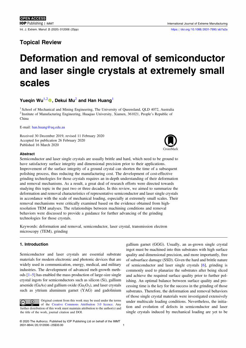
Wu et al [28, 60] utilized nanoscratch to systematicallyinvestigate the deformation pattern of single crystal Si atextremely low stress levels with the aid of HRTEM. Asshown in figure 15(a) [28], only stacking faults weregenerated underneath the α-Si layer when the applied loadwas extremely low. The SAED pattern as seen in the inset infigure 15(c) shows that the maximum intensity of the diffusediffraction ring (caused by α-Si) intersects with the {111}*
diffraction spots of the Si-I phase, suggesting that α-Si couldbe transformed directly from Si-I phase. This is significantlydifferent from the well-documented transformation route ofmonocrystalline Si induced by nanoindentation [36, 115,116]. As mentioned above, lateral loading was found to play akey role in the amorphization of Si during nanoscratching,stacking faults and twins were nucleated at a threshold loadlower than that for the nucleation of dislocations [60].Dislocations started to be generated along Si {111} planesand penetrated into the Si substrate when the load was furtherincreased as evidenced in figures 15(b) and (c) [28]. Further,HRTEM observations revealed that the dislocation inducedby nano-scratching was a total dislocation with a Burgersvector of ½ ⟨110⟩ [110]. The threshold load for the emissionof dislocations during scratching was predicted by Fang et alusing an analytical model [117]. It was proposed that thethreshold load for dislocation nucleation during nanoscratch-ing was always lower than that during nanoindentation,confirming the important role of lateral force in the generationof crystallite defects. When the scratching-induced stress wassufficiently great, α-Si was reversely recrystallized into Si-Inanocrystals, and high pressure Si-III and Si-XII phases werealso formed inside the α-Si matrix, as presented infigure 15(d) [28, 60]. Ductile mode scribing in Si was foundto be crystallographic orientation dependent [118]: (i) ductileremoval preferentially occurred in (111) plane to (110) plane,(ii) the (001) plane exhibited to be more brittle duringnanoscratching, and (iii) in the same crystal plane scratchingalong the ⟨111⟩ direction exhibited more ductile removal thanthat along the ⟨100⟩ direction.
Stress distribution is closely related to the tip geometryand its effect on the ductile-to-brittle transition wasinvestigated using spherical tips with variable radii [119]. Itwas found that a larger tip radius tended to induce surfacecracks, while sharp tips were prone to create median and/orlateral cracks. Also, friction would affect the critical depth ofcut (DOC), as lowering the friction coefficient resulted in ahigher critical DOC [119].
To more truly reveal the deformation pattern of Si in agrinding process, scratching was conducted at the speedsvarying from several to tens of meters per second [120–123],which is significantly higher than that achievable innanoscratch (at the scale of micrometers per second). Whenthe scratching depth was sufficiently small, an amorphouslayer was formed directly on the top of pristine Si-I prior to
11
Int. J. Extrem. Manuf. 2 (2020) 012006 Topical Review
the formation of chips. When scratching depth wassufficiently high, high pressure phases and α-Si coexisted inthe scratch grooves and the ratio of α-Si phase to highpressure phases increased with the increase of scratchingspeed [123]. The results are consistent with the conventionalnanoscratch experiments [28, 103], indicating that nano-scratching at a relatively low speed does mimic the Sideformation occurred in the grinding process. In other words,the scratching speeds might only affect the value of thecritical DOC, but not change the deformation pattern ofSi [124].
Local temperature in the deformation zone will unavoid-ably rise in the grinding process, even though coolant wasusually used. Thus, knowledge of the scratch-induceddeformation in Si at elevated temperatures is important ingaining a complete understanding of the deformationmechanism in grinding. It was found that scratch hardnessof Si decreased up to 46% as temperature increased fromroom temperature to 500 °C [125]. It was also reported thatscratch depth and width increased at elevated temperaturesdue to the thermal softening effect [125]. As a consequence,the surface roughness of Si wafers being processed by micro-
laser assisted machining could be improved [126]. It isinteresting to note that high-pressure Si phase was absent inthe scratched tracks at 500 °C as reported by Chavoshi et al[125]. While using similar high temperature scratchingmethod, Alreja et al reported the presence of metastablesilicon phases under various furnace-controlled temperatureconditions, i.e. RT to 500 °C [127]. Nanoscratching atelevated temperatures is still at the infancy stage and it isexpected that the complication at relatively high temperaturesmay cause some controversial results.
Molecular dynamics analysis would help understand thedeformation of Si under diamond asperities to simulate nano-sliding [128, 129] and nano-scratching [130]. Through MDsimulation, it was found that a thin amorphous layer alwaysexisted on the top of the deformed Si, but there was absenceof dislocations when the penetration depth of asperity wassufficiently small [129]. Four-coordinated diamond cubicsilicon can be transformed into the six-coordinated β-siliconform when the penetration depth or the stress being inducedwas sufficiently high [129]. Importantly, the transformation ofβ-phase to the amorphous phase of Si is reversible. It shouldbe noted that MD models could only simulate very limited
Figure 15. Cross-sectional TEM images of the nanoscratches created with different loads of (a) 0.2, (b) 0.5, (c) 4 and (d) 6 mN. The insets in(c) and (d) are the SAED patterns acquired from the circled region in (c) and (d), respectively. Reprinted from [28], Copyright 2010, withpermission from Elsevier Ltd. on behalf of Acta Materialia Inc. All rights reserved.
12
Int. J. Extrem. Manuf. 2 (2020) 012006 Topical Review

penetration depth, at a scale of several nanometers, which wasmuch smaller than the depths used in nanoscratch, usuallyseveral tens or hundreds of nanometers. Therefore, MDsimulation cannot fully represent a pragmatic nanoscratchingprocess.
Overall, the deformation pattern of single crystal Siinduced by nanoscratching includes amorphization, twinning,formation of stacking faults, dislocation and high pressurephases, and recrystallization when the deformation is atextremely small scales.
3.2.2. Deformation of GaAs under nanoscratch. Little wasdone to study the deformation of GaAs using nanoscratching[85, 131–135]. Micro-scratches made using diamond tips ofvariable geometries (cube corner, conical, and Berkovich)were used to investigate the mechanics of GaAs deformationfor industrial applications [132, 133]. Wasmer et al creativelycut the longitudinal TEM lamellae along a scratch, whichmakes it possible to directly compare the crystal defectsinduced from indenting and scratching [85]. Figure 16 showsthat twinning was the main deformation mechanism underindentation, whereas only slip bands and perfect dislocationswere induced during scratching.
The effect of peak normal load on the deformationpattern of GaAs under nanoscratching was investigated byWu et al [136]. As shown in figure 17(a), the impression wasvery shallow when the load was small (i.e. 1 mN in this case)and only slight pile-up appeared on the shoulder of thenanoscratch, which was also observed in previous studies[85, 95]. When the normal load was sufficiently high, amedian crack was initiated [95, 96, 137], as shown infigure 17(b). The crack was initiated and propagated in aperpendicular direction into GaAs bulk. Previous studiessuggested that median cracks could be initiated due to highstress concentration underneath spherical [84] and Berkovichtips [67]. It was verified by the HRTEM results as shown in
figure 17(c) that parallel platelets, which were determined tobe a twinning structure, can be clearly seen in the area nearthe scratch impression. Note the white lines in figure 17(c)indicated the reflective atomic planes which were character-istics of a twinning structure. The density of twins increasedwith the increased applied normal load [136]. Moreover, thetwinning structure was also verified by an SAED analysis asshown in figure 17(d). Diffraction spots, indicated by thewhite arrows in figure 17(d), were superimposed on a<110>diffraction pattern of GaAs, which represents thediffraction from the reflective twinning planes. Parlinska-Wojtan et al [95] proposed that during nanoindentation, if thetip apex angle was larger than 70.5°, namely the anglebetween two {111} planes in GaAs, there would beconvergent twinning patterns formed during nanoindentation;otherwise, divergent twinning patterns were expected. Bothconvergent and divergent twinning patterns were seen infigure 17, this might be due to the difference in tip geometryand the effect of lateral force. Direct evidence of latticebending induced by nanoscratching at atomic level wasdemonstrated by Wu et al and it appeared to be a newdeformation pattern in GaAs, in addition to previouslyreported dislocation, twinning and stacking faults [135].
3.2.3. Deformation of laser crystals under nanoscratch. Theknowledge of nanoscratch-induced deformation of lasercrystals was rarely reported. Li et al conducted somescratching studies on GGG crystals using a Berkovich tip[16, 138], with which the brittle to ductile transition for thiscrystal was investigated. Amorphization and formation ofnano-crystals were found to be the dominated deformationpatterns in the plastic flow zone [16]. Micro cracks would begenerated when the normal force was increased beyond athreshold value and median cracks would be initiated whenthe normal force was sufficiently high. The effect of strainrate on the scratch-induced deformation of GGG was alsoreported [138] and increasing the scratching velocity couldeffectively improve plasticity and reduce the critical depth forbrittle-to-ductile transition. As shown in figure 18, nano-sizedpolycrystals and amorphous phases were found to be thedominated crystal defects in the scratched GGG, irrelevant ofscratching velocity [138]. The corresponding TEM resultsindicated that the increased scratching velocity led to slippingplanes appearing in multiple directions as shown infigure 19(b), which subsequently prevented the generationof long slipping planes and hence reduced the depth of SSD.In other words, the depth of damaged layer decreased with theincreasing of scratching velocity, as indicated by the yellowarrows in figure 19.
Surface morphologies of the YAG single crystalscratched by a Berkovich tip with a tip radius of 2 μm wasexamined by Li et al with the aid of SEM [100]. Their workenabled the identification of the critical load for the ductile-to-brittle transition of this crystal, as the first radial crack wasobserved on the scratched surface when the applied load wasapproximately 18 mN in this case. It should be noted that theductile-to-brittle transition was judged based on the surface
Figure 16. TEM images of a FIB lamella prepared using transversecutting through an indent at the beginning of the scratch performedwith a spherical indenter: (a) general view, (b) detailed bright fieldview of the area under the indent, and SAED patterns taken from theareas under (c) the scratch and (d) the indent. Reprinted from [85],with the permission from AIP Publishing.
13
Int. J. Extrem. Manuf. 2 (2020) 012006 Topical Review

cracks, rather than a complete understanding of subsurfacedamage, which could underestimate the critical load.
4. Deformation and removal of single crystalsinvolved in machining
Grinding, cutting, lapping, and polishing are the mainmachining approaches currently used for the fabrication ofsemiconductor wafers and laser crystal substrates. Grinding is
often used for stock removal to achieve the required thick-ness, flatness and parallelism, while lapping and mechanicalpolishing processes are employed for the removal of theresidual damage layer after grinding to obtain the requiredsurface integrity. Thus if the grinding process can minimizeits residual damaged layer, the processing time for the finalfinishing process can be reduced, thus lowering the overallmanufacturing cost. In the applications, the quality require-ment of semiconductor and laser crystal wafers is so stringentthat an atomically smooth surface and a damage-free
Figure 17. High magnification TEM images of the nanoscratches made using a conical tip at different loads of (a) 1 and (b) 6 mN, (c)HRTEM image taken at the shoulder of a scratch, showing twinning structure and (d) its corresponding SAED pattern [136].
Figure 18. (a) Bright field TEM image of scratched GGG single crystal, HRTEM images showing (b) nanocrystals and (c) amorphous [16].
14
Int. J. Extrem. Manuf. 2 (2020) 012006 Topical Review

subsurface must be guaranteed. To achieve this, knowledge ofthe deformation and removal of those crystal materialsinvolved in machining need to be explored. It should also benoted that as grinding, lapping and polishing are usuallyemployed in the process, the three procedures should beoptimized in order to reduce the overall manufacturing cost.This suggests that different processing combinations may beadopted for different crystals. Nevertheless, subsurfacedamage, or SSD, cannot be fully removed after grinding/lapping/mechanical polishing [139]. Therefore, a final fin-ishing process usually employs chemical mechanical polish-ing (CMP) that can generate atomically smooth and damagefree surfaces [140–142]. As SSD must be removed in the finalfinish process, the smallest possible SSD layer generated ingrinding/lapping/polishing is very beneficial to its sub-sequent process, in terms of machining efficiency and cost[143]. It should be noted that this review does not cover thedeformation and removal involved in CMP process because itconcerns a great deal of chemically enhanced materialremoval. Also, grinding at nanoscale, lapping and mechanicalpolishing are all abrasive machining processes involvingsimilar grit-work material interactions, so that in this workonly the literatures concerning grinding induced deformationand removal will be reviewed.
4.1. Fundamentals of brittle-to-ductile transition
Grinding is an abrasive machining process that has beenextensively used to machine semiconductor substrates andlaser crystals to achieve the desired surface roughness anddimensional precision [44, 46, 143–149]. To achieve a highprecision finish surface, ultrafine grain of diamond isemployed to generate ductile-like deformation and removal.Grinding processes are, however, very complicated, owing totheir complex stress status and the elevated temperatures inthe grinding zone. The work material experiences repeatedrubbing, plowing, scratching, and shearing by multiple dia-mond grits, thus the aforementioned deformation mechanismsof single crystals under instrumented mechanical loading maybe used as a guide for optimizing the grinding process.
To achieve the best possible surface integrity in thegrinding of semiconductor and laser crystal materials that arevery brittle, their material deformation and removal should
not involve brittle fracture or cracking. In other words, thegrinding must be carried out in the so called ‘ductile’ removalregime. The effect of DOC on the brittle-to-ductile transitionin the grinding of brittle materials may be understood with theaid of Bifano’s model, in which the critical grinding depth canbe estimated as [9]:
⎜ ⎟⎛⎝
⎞⎠ ( )= Yd
E
H
K
H, 1c
c2
where E is the material’s Young’s modulus, H is hardness, Kc
is fracture toughness, and Ψ is material’s brittle-ductiletransition factor, which varies with different brittle materials.Bifano’s model provides the criteria for the occurrence ofductile removal in the grinding process when the DOC ofindividual abrasive is smaller than dc. The DOC of an indi-vidual abrasive grit can be estimated by calculating themaximum undeformed chip thickness (hm). hm for facegrinding can be calculated as [150]:
⎜ ⎟⎛⎝
⎞⎠
⎛⎝⎜
⎞⎠⎟ ( )=h
Cr
f
v
2, 2m
s
0.5 0.5
where C is the density of active abrasives, r is the width todepth ratio for an undeformed chip, f is the feed rate and vs isthe wheel velocity. The value of hm for surface grinding canbe calculated using the following equation [151]:
⎜ ⎟⎛⎝
⎞⎠
⎛⎝⎜
⎞⎠⎟
⎛⎝⎜
⎞⎠⎟ ( )
a=h
C
v
v
a
d
3
tan, 3m
w
s
e
s
0.5 0.5 0.25
where C is the density of active abrasives, α is the semi-included angle for the undeformd chip cross section, ds is thewheel diameter, vw is the workpiece feed rate, vs is the wheelspeed and ae is the wheel DOC. Based on Bifano’s model, toenable the ductile-like removal in the grinding of a brittlesolid, the grinding parameters must be designed so that hm issmaller than dc. It should be mentioned that this model workswell for some brittle materials, but could considerablyunderestimate or overestimate the critical depth for ductileremoval due to the complex nature of abrasive machining andmicrostructure of brittle materials.
Figure 19. TEM images of subsurface damage of GGG single crystal at different scratching velocities (a) v=0.1 μm s−1 and (b) v=100 μm s−1. Reprinted from [138], Copyright 2019, with permission from Elsevier.
15
Int. J. Extrem. Manuf. 2 (2020) 012006 Topical Review

4.2. Grinding induced deformation and removal of Si
The characteristics and performance in the grinding of singlecrystal Si were intensively investigated, including the effectsof grinding wheels [46, 140, 143, 152], grinding inducedsurface/subsurface damages [46, 153–155], and optimizationof grinding parameters for better surface quality [44, 144,148, 153, 156–164]. As the material removal involved insilicon grinding is often controlled at nanometric scales toensure the ductile-like removal [153, 155, 160–163], such agrinding process was also termed as nanogrinding. In thiswork, only the deformation and removal of single crystal Sicarried out in the ductile region will be reviewed.
The grit size of a grinding wheel plays a critical role inthe deformation and ductile-like removal of Si. AFM imagingof the ground Si surface demonstrated that grinding grooveswere apparent and became finer as the grit size decreased[153]. The grit size effect on subsurface damage wasextensively examined by use of cross-sectional TEM[153, 155, 165], and the amorphous, elastically stressed, andplastically deformed layers were found to be the maindeformation structures, as shown in figure 20 [155]. When agrinding wheel with a fine grit size of 3000 in mesh was used,only pure amorphous phase and elastically stressed layer wereobserved in ground Si monocrystal, as evidenced in the TEMimage in figure 20(a) and its corresponding SAED pattern infigure 20(b). No evidence of nanocrystals was found in theamorphous layer. In contrast, when a diamond wheel with acoarser grit size was used, severely deformed layer wasobserved in the ground Si as shown in figure 20(c) andnanocrystals with the same crystal structure as the pristine Siwere formed based on the SAED pattern shown infigure 20(d). The subsurface with a more severely damagedlayer was obtained when a very coarse grit wheel was used, asshown in figure 20(e) and nanocrystals other than the Si-Iphase were also confirmed by the SAED pattern infigure 20(f). HRTEM images of the nanocrystals embedded inthe amorphous in figure 20(e) are shown in figures 20(g) and(h), demonstrating the existence of high pressure phase of Si-III. The residual stress, after rough and fine grinding, wasfound to be in the range of a few hundreds of MPa and tens ofMPa, respectively [165]. To sum up, less severely damagedsubsurface layer can be obtained using grinding wheels withfiner grit sizes, but sacrificing the material removal rate. Thus,to reduce the overall processing cost associated with grinding,an optimal combination of grinding procedures with differentgrit sizes is necessary, such as a coarser wheel for removalwhile a finer wheel for finishing.
The conventionally used mesh sizes of grinding wheelsfor silicon machining were below 5000, corresponding to gritsize of above ∼2 μm. As a consequence, the surface rough-ness (Ra) of a ground Si wafer was above 8 nm [153, 158]and the depth of subsurface damage layer was in the scale of100–200 nm [153, 155, 166]. To further improve the surfacefinishing by grinding, an ultrafine diamond wheel of a gritsize of 0.25 μm could be adopted, which would produce anextremely smooth surface of an average roughness of 0.6 nm[46]. The TEM examination indicated that the total thickness
of subsurface damage layer was less than 60 nm, as shown infigure 21 [46]. The grinding results indicate that the damagedlayer needs to be removed in the following polishing processis less than 100 nm, which is promising and exaggerates thepossibility to be adopted in the product line. However, itshould be noted that the grinding conditions became moresophisticated when an ultrafine grinding wheel wasemployed, i.e. inappropriate grinding parameters would causeburning as the wheel could be easily overloaded and thusmore grinding heat would be generated [46]. The phasetransformation of Si wafer under various grinding conditionswere investigated using HRTEM [154] and the formation ofnanocrystals appeared to be strongly influenced by the ther-mal status of a grinding process when using a diamond wheelwith ultrafine grits. Specifically, the higher grinding heatbeing generated would enhance the transformation of Si-I tohigh-pressure Si phases [154]. Note that the wheel speedwould also affect the ground surface in term of the depth of adamaged layer, but its effect is less significant [46].
For face grinding of a Si substrate or wafer, the wheeldiameter is generally sufficiently large to cover the entireworkpiece in one grinding revolution [46, 157]. Certainly, asmaller diamond wheel would help reduce the processing cost[152]. By carefully planning the cutting paths of the smallerwheel, it is possible to achieve a surface roughness similar toor slightly worse than that obtained using the conventionallarge wheel [152]. In this case, a mathematical model wasdeveloped to plan the cutting path, which helped to optimizethe grinding conditions too. Nevertheless, a grinding wheelwith diameter slightly larger than the wafer radius should bebeneficial to improve the grinding performance.
Three dimensional MD model was established for thehigh speed grinding of Si by Li et al [167] to understand thespeed effect on the integrity of ground surface and SSD. Theequivalent stress distribution and corresponding atomic dis-placement in the ground Si material are illustrated infigures 22(a) and (b), respectively. It was found that a highergrinding velocity would produce larger chips and higher localtemperature in grinding zone, which might help reduce SSD.However, at extremely high grinding speed, the subsurfacedamage layer was slightly thicker because elevated temper-ature might promote the nucleation and motion of disloca-tions [167].
Deionized water is usually employed as the coolant in thegrinding of Si substrates [46, 159]. It is suggested that bothinner and outer coolant nozzles should be used simulta-neously to achieve the best possible results and a high flowrate was beneficial for the cooling performance [159]. Li et alproposed that water-based coolants containing grapheneoxide could significantly reduce the tangential force duringgrinding and thus improve surface/subsurface quality [168].
4.3. Grinding induced deformation and removal of β-Ga2O3
The grinding characteristics of single crystal β-Ga2O3 wereseldom reported, most likely because it is a newly developedmaterial. Nanogrinding induced surface/subsurface defor-mation characteristics of single crystal β-Ga2O3 were
16
Int. J. Extrem. Manuf. 2 (2020) 012006 Topical Review

Figure 20. Bright-field TEM images and corresponding SAED patterns of ground Si using grinding wheels with mesh size of (a) and(b) 3000, (c) and (d) 800, (e) and (f) 400, respectively. (g), (h) HRTEM images of the nanocrystals embedded in the amorphous in(e). Reproduced from [155]. © IOP Publishing Ltd. All rights reserved.
17
Int. J. Extrem. Manuf. 2 (2020) 012006 Topical Review

investigated by Gao et al [20]. The severity of SSD wasreportedly reduced when grinding wheels with finer grit sizeswere employed. A typical TEM image and its correspondingHRTEM image of the ground β-Ga2O3 single crystal using an
ultrafine grinding wheel of mesh size of 12 000 are shown infigures 23(a) and (b), respectively. Formation of nanocrystals,stacking faults, twins, and dislocations were the mainmechanisms responsible for the deformation induced by
Figure 21. Cross-sectional TEM images of the ground Si using a grinding wheel of 12 000 in mesh with different wheel speeds of (a) 36.6and (b) 29.3 m s−1 and a fixed feed rate of 6 μmmin−1. Reprinted from [46], Copyright 2010, with permission from Elsevier.
Figure 22. (a) Equivalent stress distribution and (b) atomic displacement in the ground Si. Reprinted from [167], Copyright 2015, withpermission from Elsevier.
Figure 23. (a) Cross-sectional TEM image examined along the [010] direction of the β-Ga2O3 ground using a grinding wheel of mesh size of12 000, and (b) HRTEM image taken from the solid boxed area in (a), where the insets are the corresponding SAED patterns. Reprinted from[20], Copyright 2018, with permission from Elsevier.
18
Int. J. Extrem. Manuf. 2 (2020) 012006 Topical Review

grinding, which are similar to what were found from thestudies using instrumented mechanical loading [17]. Differentfrom the deformation features induced by nanoindentationand nanoscratch, an amorphous phase was found in theground samples when the specific grinding energy was sig-nificantly high, which was observed after the occurrence ofother crystallite defects. The deformation pattern in the ductileregime of this crystal material was summarized in figure 24. Itwas also found that the hardness of grinding-induceddeformed layer was higher than that of the pristine β-Ga2O3
crystal, which was most likely attributed to the effects ofnanocrystals [20]. Both thickness and hardness of the SSDlayer were reduced when finer grit sizes were used as a resultof the chip thickness reduction. Overall, the mechanismresponsible for the ductile deformation of β-Ga2O3 was foundto be related to the intrinsic stacking fault energy and thespecific grinding energy being used [20].
4.4. Grinding induced deformation and removal of lasercrystals
The literature study showed that YAG single crystals aremainly machined through lapping and polishing that are lessaggressive processes with lower dimensional accuracy thangrinding [21, 169]. The studies regarding the grindingperformance of this crystal material was rarely reported. Liet al investigated the precision grinding performance ofYAG single crystals using different grit size wheels [21].Two types of ground surfaces, namely ductile-like andbrittle-ductile surfaces, were obtained. The grinding inductile regime was realized using the diamond wheels withmesh sizes of 4000 and 6000. Slippages of (001) crystalplanes were evidenced in the subsurface, as presented infigure 25 [21], along with the formation of stacking faults,dislocations, and distortion of atomic planes, which areshown in the HRTEM images in figures 26(a)–(e). Gen-eration of brittle-ductile surfaces was attributed to theplastic deformation with formation of nanocrystals andnanovoids, as well as brittle fracture, when the grindingwheel with a coarser grit size was employed. As shown infigure 27, a model that depicts the effect of grit distributionon the chip formation, combines with other materialsdeformation models, was developed to estimate the grindingforce in the ductile-like removal of the grinding process byconsidering the combined effect of strain rate, randomdistribution of abrasive radii, and elastic-to-plastic trans-ition depth [6]. It is believed that accuracy of the predictedgrinding force was substantially improved by taking theeffect of strain rate into account. The thickness of damagedlayer is about 200 nm with slippages along particular latticeplanes. To further improve the surface quality in terms ofreducing damaged layer thickness and eliminating slippage,a grinding wheel with finer diamond grits should be adoptedand grinding parameters need further optimization in termsof grinding force and surface finish.
5. Summary and perspectives
In this work, the deformation and removal characteristics andbehaviors of representative semiconductor and laser crystals,including Si, GaAs, β-Ga2O3, YAG and GGG single crystals,were systematically reviewed based on the available litera-ture. The deformation and removal patterns induced byinstrumented mechanical loads and grinding were summar-ized in table 2 for comparison purpose. This review demon-strates that the knowledge of deformation and removalmechanisms obtained from nanoindentation and nanoscratchstudies can be utilized to optimize the grinding processes forthose important single crystals, which are thus beneficial toimproving their surface finish and manufacturing cost.
From this review it is clear that knowledge of thedeformation and removal characteristics and behaviors of aspecific single crystal gained from the previous studies shouldbe taken into consideration for developing abrasive technol-ogies for the crystal. It is thus important to use instrumented
Figure 24. Schematic illustration of the ground subsurface of singlecrystal Ga2O3. Reprinted from [20], Copyright 2018, with permis-sion from Elsevier.
Figure 25. TEM image of subsurface of the ground YAG singlecrystal using a grinding wheel of mesh size of 6000. Reprinted from[21], Copyright 2019, with permission from Elsevier.
19
Int. J. Extrem. Manuf. 2 (2020) 012006 Topical Review

nanoindentation and nanoscratch to gain its deformation andremoval characteristics, as those approaches can producesimilar deformation patterns and mechanisms to a grindingprocess. The first-hand knowledge being obtained should save
a lot of testing time for developing optimal grinding, lappingand polishing processes.
In general, the grit DOC involved in the grinding of thosebrittle single crystals plays a critical role in determining their
Figure 26. High magnification TEM images of subsurface of the ground YAG single crystal acquired from the square marked area shown infigure 25, showing (a) a slip plane and (b) termination of a slip plane, and (c)–(e) HRTEM images obtained from the denoted rectanglesmarked in (b) showing the dislocations, stacking faults and atomic plane distortion. Reprinted from [21], Copyright 2019, with permissionfrom Elsevier.
Figure 27. Schematic diagrams of (a) trajectory of diamond abrasives, (b) hm of a single abrasive and (c) the distribution of diamondabrasives. Reprinted from [21], Copyright 2019, with permission from Elsevier.
20
Int. J. Extrem. Manuf. 2 (2020) 012006 Topical Review

deformation and removal behaviors. More specifically, whenthe grit DOC in a grinding process is smaller than the criticalDOC for brittle-to-ductile transition for a specific crystalmaterial, ductile-like deformation and removal should occur,which enables the achievement of appropriate surface finishand subsurface integrity. Usually, a grinding wheel with finerdiamond grits produces a better surface finish with less sur-face/subsurface damage. However, special care is needed toavoid wheel burning when dealing with ultrafine grindingwheels. Certainly, grinding wheels with relatively coarsediamond grits are more suitable for stock removal, but moresignificant subsurface damage would be generated, whichthus increases difficulty of the subsequent finishing process,prolongs machining time, and increases the overall manu-facturing cost. It is thus of great value to have a completeunderstanding of the deformation and removal mechanisms ofthe crystal material involved in all the finishing procedures, sothat an optimal protocol can be established from both qualityand efficiency perspectives. Optimization of grinding condi-tions to minimize subsurface damage should be the ultimategoal in an abrasive finishing process, though it is impossibleto eliminate crystalline defects. Nevertheless, optimizationshould also be made with taking care of appropriatemachining efficiency.
Acknowledgments
The authors would like to acknowledge the financial supportsfrom Australia Research Council (ARC) under DiscoveryProjects program (DP180103275). It is also supported by theScientific Research Funds of Huaqiao University (605-50Y19022). Certain images in this publication have beenobtained by the author(s) from the Wikipedia/Wikimediawebsite, where they were made available under a CreativeCommons licence or stated to be in the public domain. Pleasesee individual captions in this publications for details. To theextent that the law allows, IOP Publishing disclaim any lia-bility that any person may suffer as a result of accessing,using or forwarding the image(s). Any reuse rights should bechecked and permission should be sought if necessary from
the Wikipedia/Wikimedia and/or the copyright owner (asappropriate) before using or forwarding the image(s).
ORCID iDs
Yueqin Wu https://orcid.org/0000-0003-3511-4270
References
[1] Shiraishi Y, Takano K, Matsubara J, Iida T, Takase N,Machida N, Kuramoto M and Yamagishi H 2001 Growth ofsilicon crystal with a diameter of 400 mm and weight of400 kg J. Cryst. Growth 229 17–21
[2] Rudolph P and Jurisch M 1999 Bulk growth of GaAs: anoverview J. Cryst. Growth 198 325–35
[3] Galazka Z, Uecker R, Irmscher K, Albrecht M, Klimm D,Pietsch M, Brützam M, Bertram R, Ganschow S andFornari R 2010 Czochralski growth and characterization ofβ-Ga2O3 single crystals Cryst. Res. Technol. 45 1229–36
[4] Golubovic A, Nikolic S, Gajic R, Duric S and Valcic A 2002The growth of Nd:YAG single crystals J. Serb. Chem. Soc.67 291–300
[5] Liu W, Zhang Q, Sun D, Luo J, Gu C, Jiang H and Yin S2011 Crystal growth and spectral properties of Sm:GGGcrystal J. Cryst. Growth 331 83–6
[6] Vandeperre L J, Giuliani F, Lloyd S J and Clegg W J 2007The hardness of silicon and germanium Acta Mater. 556307–15
[7] Liu K, Li X P and Liang S Y 2007 The mechanism of ductilechip formation in cutting of brittle materials Int. J. Adv.Manuf. Technol. 33 875–84
[8] Antwi E K, Liu K and Wang H 2018 A review on ductilemode cutting of brittle materials Front. Mech. Eng. 13251–63
[9] Bifano T G, Dow T A and Scattergood R O 1991 Ductile-regime grinding: a new technology for machining brittlematerials J. Manuf. Sci. Eng. 113 184–9
[10] Phillips J C 1970 Bonds and bands in semiconductors: newinsight into covalent bonding in crystals has followed fromstudies of energy-band spectroscopy Science 169 1035–42
[11] Lee S 2018 Advanced Material and Device Applications withGermanium (Rijeka: IntechOpen)
[12] https://en.wikipedia.org/w/index.php?title=Silicon&oldid=944103337
[13] Baca A G and Ashby C I H 2005 Fabrication of GaAsDevices (London: The Institution of Electrical Engineers)
[14] Nakagomi S, Momo T, Takahashi S and Kokubun Y 2013Deep ultraviolet photodiodes based on β- Ga2O3/SiCheterojunction Appl. Phys. Lett. 103 072105
[15] Mihokova E, Nikl M, Mares J A, Beitlerova A, Vedda A,Nejezchleb K, Blazek K and D’Ambrosio C 2007Luminescence and scintillation properties of YAG:Ce singlecrystal and optical ceramics J. Lumin. 126 77–80
[16] Li C, Zhang F H, Meng B B, Rao X S and Zhou Y 2017Research of material removal and deformation mechanismfor single crystal GGG (Gd3Ga5O12) based on varied-depthnanoscratch testing Mater. Des. 125 180–8
[17] Wu Y Q, Gao S and Huang H 2017 The deformation patternof single crystal beta-Ga2O3 under nanoindentation Mater.Sci. Semicond. Proc. 71 321–5
[18] Li Z C, Liu L, Wu X, He L L and Xu Y B 2002 TEMobservation of the phase transition in indented GaAs Mater.Lett. 55 200–4
Table 2. Summary of the deformation and removal patterns ofsemiconductor and laser single crystals induced by mechanicalloading.
Material
Deformation Si GaAs β-Ga2O3 YAG GGG
Amorphous √ √ √ × √Twins √ √ √ × ×Dislocations √ √ √ √ √Phases transformation √ × × × ×Lattice bending √ √ √ √a ×Nanocrystals √ √ √a √a √Cracks √ √ √ √ √
a
Deformations were observed in nanogrinding only.
21
Int. J. Extrem. Manuf. 2 (2020) 012006 Topical Review

[19] Stepanov S I, Nikolaev V I, Bougrov V E and Romanov A E2016 Gallium oixde: properties and applications—a reviewRev. Adv. Mater. Sci. 44 63–86
[20] Gao S, Wu Y Q, Kang R K and Huang H 2018 Nanogrindinginduced surface and deformation mechanism of singlecrystal beta-Ga2O3 Mater. Sci. Semicond. Proc. 79 165–70
[21] Li C, Li X L, Wu Y Q, Zhang F H and Huang H 2019Deformation mechanism and force modelling of the grindingof YAG single crystals Int. J. Mach. Tool Manuf. 143 23–37
[22] Carruthers J R, Kokta M, Barns R L and Grasso M 1973Nonstoichiometry and crystal growth of gadolinium galliumgarnet J. Cryst. Growth 19 204–8
[23] Pardavi-Horváth M 1984 Microhardness and brittle fractureof garnet single crystals J. Mater. Sci. 19 1159–70
[24] Yang P Z, Deng P Z, Yin Z W and Tian Y L 2000 The growthdefects in Czochralski-grown Yb:YAG crystal J. Cryst.Growth 218 87–92
[25] Voronkov V V and Falster R 2002 Intrinsic point defects andimpurities in silicon crystal growth J. Electrochem. Soc. 149G167–74
[26] Falster R and Voronkov V V 2000 On the properties of theintrinsic point defects in silicon: a perspective from crystalgrowth and wafer processing Phys. Status Solidi b 222219–44
[27] Bradby J E, Williams J S, Wong-Leung J, Swain M V andMunroe P 2000 Transmission electron microscopyobservation of deformation microstructure under sphericalindentation in silicon Appl. Phys. Lett. 77 3749–51
[28] Wu Y Q, Huang H, Zou J, Zhang L C and Dell J M 2010Nanoscratch-induced phase transformation ofmonocrystalline Si Scr. Mater. 63 847–50
[29] Le Bourhis E and Patriarche G 2008 Structure ofnanoindentations in heavily n- and p-doped (001) GaAs ActaMater. 56 1417–26
[30] Bhat H L 2015 Introduction to Crystal Growth: Principlesand Practice (London: Taylor and Francis)
[31] Queisser H J and Haller E E 1998 Defects in semiconductors:some fatal, some vital Science 281 945–50
[32] Mujica A, Rubio A, Munoz A and Needs R J 2003 High-pressure phases of group-IV, III-V, and II-VI compoundsRev. Mod. Phys. 75 863–912
[33] Rapp L, Haberl B, Pickard C J, Bradby J E, Gamaly E G,Williams J S and Rode A V 2015 Experimental evidence ofnew tetragonal polymorphs of silicon formed throughultrafast laser-induced confined microexplosion Nat.Commun. 6 7555
[34] Domnich V G , Y 2002 Phase transformations in silicon undercontact loading Rev. Adv. Mater. Sci. 3 1–36
[35] Yin M T and Cohen M L 1980 Microscopic theory of thephase-transformation and lattice-dynamics of Si Phys. Rev.Lett. 45 1004–7
[36] Hu J Z, Merkle L D, Menoni C S and Spain I L 1986 Crystaldata for high-pressure phase of silicon Phys. Rev. B 344679–84
[37] Kim D E and Oh S I 2006 Atomistic simulation of structuralphase transformations in monocrystalline silicon induced bynanoindentation Nanotechnology 17 2259–65
[38] Chrobak D, Nordlund K and Nowak R 2007 Nondislocationorigin of GaAs nanoindentation pop-in event Phys. Rev.Lett. 98 045502
[39] Wu K H, Yan X Q and Chen M W 2007 In situ Ramancharacterization of reversible phase transition in stress-induced amorphous silicon Appl. Phys. Lett. 91 101903
[40] Demangeot F, Puech P, Domnich V, Gogotsi Y G, Pinel S,Pizani P S and Jasinevicius R G 2002 Raman mappingdevoted to the phase transformation and strain analysis in Simicro-indentation Adv. Eng. Mater. 4 543–6
[41] Gogotsi Y, Baek C and Kirscht F 1999 Ramanmicrospectroscopy study of processing-induced phase
transformations and residual stress in silicon Semicond. Sci.Technol. 14 936–44
[42] Kailer A, Nickel K G and Gogotsi Y G 1999 Ramanmicrospectroscopy of nanocrystalline and amorphous phasesin hardness indentations J. Raman Spectrosc. 30 939–46
[43] Huang H, Chen W K and Kuriyagawa T 2007 Profile errorcompensation approaches for parallel nanogrinding ofaspherical mould inserts Int. J. Mach. Tool Manuf. 472237–45
[44] Pei Z J, Fisher G R, Bhagavat M and Kassir S 2005 Agrinding-based manufacturing method for silicon wafers: anexperimental investigation Int. J. Mach. Tool Manuf. 451140–51
[45] Zhang Z Y, Guo D M, Kang R K, Gao H, Jin Z J andMeng Y W 2010 Subsurface crystal lattice deformationmachined by ultraprecision grinding of soft-brittle CdZnTecrystals Int. J. Adv. Manuf. Technol. 47 1065–81
[46] Zhang Z Y, Huo F W, Wu Y Q and Huang H 2010 Grindingof silicon wafers using an ultrafine diamond wheel of ahybrid bond material Int. J. Mach. Tool Manuf. 51 18–24
[47] Zhang Z Y, Meng Y W, Guo D M, Wu L L, Tian Y J andLiu R P 2010 Material removal mechanism of precisiongrinding of soft-brittle CdZnTe wafers Int. J. Adv. Manuf.Technol. 46 563–9
[48] Zhou L B, Shimizu J, Shinohara K and Eda H 2003 Three-dimensional kinematical analyses for surface grinding oflarge scale substrate Precis. Eng. 27 175–84
[49] Bradby J E, Williams J S, Wong-Leung J, Swain M V andMunroe P 2001 Mechanical deformation in silicon by micro-indentation J. Mater. Res. 16 1500–7
[50] Chang L and Zhang L C 2009 Deforamtion mechanisms atpop-out in monocrystalline silicon under nanoindentationActa Mater. 57 2148–53
[51] Wu Y Q, Yang X Y and Xu Y B 1999 Cross-sectionalelectron microscopy observation on the amorphizedindentation region in [001] single-crystal silicon Acta Mater.47 2431–6
[52] Zarudi I, Zhang L C and Swain M V 2003 Behavior ofmonocrystalline silicon under cyclic microindentations witha spherical indenter Appl. Phys. Lett. 82 1027–9
[53] Zhang L C and Tanaka H 1999 On the mechanics and physicsin the nano-indentation of silicon monocrystals JSME Int. J.A 42 546–59
[54] Zarudi I, Zhang L C, Cheong W C D and Yu T X 2005 Thedifference of phase distributions in silicon after indentationwith Berkovich and spherical indenters Acta Mater. 534795–800
[55] Yan J W, Takahashi H, Gai X H, Harada H, Tamaki J andKuriyagawa T 2006 Load effects on the phasetransformation of single-crystal silicon duringnanoindentation tests Mater. Sci. Eng. A 423 19–23
[56] Ruffell S, Bradby J E, Williams J S and Munroe P 2007Formation and growth of nanoindentation-induced highpressure phases in crystalline and amorphous silicon J. Appl.Phys. 102 063521
[57] Jang J I, Lance M J, Wen S Q, Tsui T Y and Pharr G M 2005Indentation-induced phase transformations in silicon:influences of load, rate and indenter angle on thetransformation behavior Acta Mater. 53 1759–70
[58] Ge D B, Domnich V and Gogotsi Y 2003 High-resolutiontransmission electron microscopy study of metastable siliconphases produced by nanoindentation J. Appl. Phys. 932418–23
[59] Bradby J E, Williams J S and Swain M V 2003 In situelectrical characterization of phase transformations in Siduring indentation Phy. Rev. B 67 085205
[60] Wu Y Q, Huang H, Zou J and Dell J M 2009 Nanoscratch-induced deformation of single crystal silicon J. Vac. Sci.Technol. B 27 1374–7
22
Int. J. Extrem. Manuf. 2 (2020) 012006 Topical Review

[61] Zarudi I, Zou J, McBride W and Zhang L C 2004 Amorphousstructures induced in monocrystalline silicon by mechanicalloading Appl. Phys. Lett. 85 932–4
[62] Zhang L C and Zarudi I 2001 Towards a deeperunderstanding of plastic deformation in mono-crystallinesilicon Int. J. Mech. Sci. 43 1985–96
[63] Zarudi I and Zhang L C 1999 Structure changes in mono-crystalline silicon subjected to indentation - experimentalfindings Tribol. Int. 32 701–12
[64] Zhang Z Y, Cui J F, Chang K K, Liu D D, Chen G X,Jiang N and Guo D M 2019 Deformation induced newpathways in silicon Nanoscale 11 9862–8
[65] Minor A M, Lilleodden E T, Jin M, Stach E A,Chrzan D C and Morris J W 2005 Room temperaturedislocation plasticity in silicon Phil. Mag. 85 323–30
[66] Ruffell S, Bradby J E and Williams J S 2006 High pressurecrystalline phase formation during nanoindentation:amorphous versus crystalline silicon Appl. Phys. Lett. 89091919
[67] Lloyd S J, Molina-Aldareguia J M and Clegg W J 2001Deformation under nanoindents in Si, Ge, and GaAsexamined through transmission electron microscopyJ. Mater. Res. 16 3347–50
[68] Zarudi I, Zou J and Zhang L C 2003 Microstructures ofphases in indented silicon: a high resolution characterizationAppl. Phys. Lett. 82 874–6
[69] Lin Y H, Jian S R, Lai Y S and Yang P F 2008 Moleculardynamics simulation of nanoindentation-induced mechanicaldeformation and phase transformation in monocrystallinesilicon Nanoscale Res. Lett. 3 71–5
[70] Lin Y H, Chen T C, Yang P F, Jian S R and Lai Y S 2007Atomic-level simulations of nanoindentation-induced phasetransformation in mono-crystalline silicon Appl. Surf. Sci.254 1415–22
[71] Jeong S M and Kitamura T 2007 Atomistic simulation on thephase transformation of silicon under nonhydrostatic stressJapan. J. Appl. Phys. 1 5924–9
[72] Cheong W C D and Zhang L C 2000 Molecular dynamicssimulation of phase transformations in silicon monocrystalsdue to nano-indentation Nanotechnology 11 173–80
[73] Ivashchenko V I, Turchi P E A and Shevchenko V I 2008Simulations of indentation-induced phase transformations incrystalline and amorphous silicon Phys. Rev. B 78 035205
[74] Schall J D, Gao G and Harrison J A 2008 Elastic constants ofsilicon materials calculated as a function of temperatureusing a parametrization of the second-generation reactiveempirical bond-order potential Phys. Rev. B 77 115209
[75] Luo Y R 2003 Bond Dissociation Energies (Boca Raton, FL:CRC Press) p 65
[76] Wang S and Pirouz P 2007 Mechanical properties of undopedGaAs: III. Indentation experiments Acta Mater. 55 5526–37
[77] Taylor C R, Malshe A P, Salamo G, Prince R N, Riester L andCho S O 2005 Characterization of ultra-low-load (mu N)nanoindents in GaAs(100) using a cube corner tip SmartMater. Struct. 14 963–70
[78] Patriarchey G, Largeau L, Riviere J P and Le Bourhis E 2004Vickers indentation of thin GaAs(001) samples Phil. Mag.84 3281–98
[79] Patriarche G and Le Bourhis E 2003 Plasticity of misoriented(001) GaAs surface J. Mater. Sci. Lett. 22 565–7
[80] Largeau L, Patriarche G, Glas F and Le Bourhis E 2004Absolute determination of the asymmetry of the in-planedeformation of GaAs(001) J. Appl. Phys. 95 3984–7
[81] Le Bourhis E and Patriarche G 2003 Effects of annealing onthe structure of GaAs(001) nanoindentations Phil. Mag. Lett.83 149–58
[82] Grillo S E, Ducarroir M, Nadal M, Tournie E and Faurie J P2003 Nanoindentation of Si, GaP, GaAs and ZnSe singlecrystals J. Phys. D: Appl. Phys. 36 L5–9
[83] Li Z C, Liu L, Wu X, He L L and Xu Y B 2002 Indentationinduced amorphization in gallium arsenide Mater. Sci. Eng.A 337 21–4
[84] Bradby J E, Williams J S, Wong-Leung J, Swain M V andMunroe P 2001 Mechanical deformation of InP and GaAsby spherical indentation Appl. Phys. Lett. 78 3235–7
[85] Wasmer K, Parlinska-Wojtan M, Gassilloud R, Pouvreau C,Tharian J and Micher J 2007 Plastic deformation modes ofgallium arsenide in nanoindentation and nanoscratchingAppl. Phys. Lett. 90 031902
[86] Bradby J E, Williams J S and Swain M V 2004 Pop-in eventsinduced by spherical indentation in compoundsemiconductors J. Mater. Res. 19 380–6
[87] Le Bourhis E and Patriarche G 1999 Transmission electronmicroscopy observations of low-load indents in GaAs Phil.Mag. Lett. 79 805–12
[88] Taylor C R, Stach E A, Salamo G and Malshe A P 2005Nanoscale dislocation patterning by ultralow loadindentation Appl. Phys. Lett. 87 073108
[89] Jian S R, Fang T H, Chuu D S and Ji L W 2006 Atomisticmodeling of dislocation activity in nanoindented GaAs Appl.Surf. Sci. 253 833–40
[90] Le Bourhis E and Patriarche G 2007 Nanoindentation responseof compound semiconductors Phys. Status Solidi c 4 3002–9
[91] Le Bourhis E and Patriarche G 2007 TEM-nanoindentationstudies of semiconducting structures Micron 38 377–89
[92] Le Bourhis E and Patriarche G 2003 Plastic deformation ofIII-V semiconductors under concentrated load Prog. Cryst.Growth Charact. 47 1–43
[93] Le Bourhis E and Patriarche G 2005 Mechcanical response ofwall-patterned GaAs surface Acta Mater. 53 1907–12
[94] Pouvreau C, Wasmer K, Hessler-Wyser H, Ganiere J D,Breguet J M, Michler J, Schulz D and Giovanola J H 2013Nanoindentation cracking in gallium arsenide: II. TEMinvestigation J. Mater. Res. 28 2799–809
[95] Parlinska-Wojtan M, Wasmer K, Tharian J and Michler J2008 Microstructural comparison of material damage inGaAs caused by Berkovich and wedge nanoindentation andnanoscratching Scr. Mater. 59 364–7
[96] Li Z C, Liu L, He L L, Xu Y B and Wu X 2001 Shear-activated indentation crack in GaAs single crystal J. Mater.Res. 16 2845–9
[97] Schuh C A 2006 Nanoindentation studies of materials Mater.Today 9 32–40
[98] Wu Y Q, Gao S, Kang R K and Huang H 2019 Deformationpatterns and fracture stress of beta-phase gallium oxidesingle crystal obtained using compression of micro-pillarsJ. Mater. Sci. 54 1958–66
[99] Li C, Zhang F H, Wang X and Rao X S 2018 Investigation onsurface/subsurface deformation mechanism and mechanicalproperties of GGG single crystal induced by nanoindentationAppl. Opt. 57 3661–8
[100] Li C, Zhang Q, Zhang Y B, Zhang F H, Wang X andDong G J 2019 Nanoindentation and nanoscratch tests ofYAG single crystals: an investigation into mechanicalproperties, surface formation characteristic, and theoreticalmodel of edge-breaking size Ceram. Int. 46 3382–93
[101] Minowa K and Sumino K 1992 Stress-induced amorphizationof a silicon crystal by mechanical scratching Phys. Rev. Lett.69 320–2
[102] Zhao X Z and Bhushan B 1998 Material removal mechanismsof single-crystal silicon on nanoscale and at ultralow loadsWear 223 66–78
[103] Gassilloud R, Ballif C, Gasser P, Buerki G and Michler J2005 Deformation mechanisms of silicon duringnanoscratching Phys. Status Solidi a 202 2858–69
[104] Youn S W and Kang C G 2006 Effect of nanoscratchconditions on both deformation behavior and wet-etchingcharacteristics of silicon (100) surface Wear 261 328–37
23
Int. J. Extrem. Manuf. 2 (2020) 012006 Topical Review

[105] Zarudi I and Zhang L C 2006 Microcracking inmonocrystalline silicon due to indentation and scratchingKey Eng. Mater. 312 345–50
[106] Jeong S N, Oh H S, Park S E and Lee H L 2003 Phasetransformation of single crystalline silicon by scratchingJapan. J. Appl. Phys. 42 2773–4
[107] Lee S H 2012 Analysis of ductile mode and brittle transitionof AFM nanomachining of silicon Int. J. Mach. Tool Manuf.61 71–9
[108] Tang F Z and Zhang L C 2014 Subsurface nanocracking inmonocrystalline Si (001) induced by nanoscratching Eng.Fract. Mech. 124–125 262–71
[109] Zarudi I, Nguyen T and Zhang L C 2005 Effect oftemperature and stress on plastic deformation inmonocrystalline silicon induced by scratching Appl. Phys.Lett. 86 011922
[110] Takagi M, Onodera K, Matsumuro A, Iwata H, Sasaki K andSaka H 2008 TEM and HRTEM observations ofmicrostructural change of silicon single crystal scratchedunder very small loading forces by AFM Mater. Trans. 491298–302
[111] Iizuka T and Okada Y 1994 Study of scratch-inducedmechanical damage on silicon (111) surfaces Japan. J. Appl.Phys. 33 1427–34
[112] Gogotsi Y, Zhou G H, Ku S S and Cetinkunt S 2001 Ramanmicrospectroscopy analysis of pressure-inducedmetallization in scratching of silicon Semicond. Sci. Technol.16 345–52
[113] Zhang C, Zhu H, Jiang Z, Huang C and Wang J 2020Removal mechanism and surface quality of crystalsemiconductor materials in scratching tests with Berkovichindenter Mater. Sci. Semicond. Process. 105 104746
[114] Wu Y Q, Huang H and Zou J 2013 A focused review onnanoscratching-induced deformation of monocrystallinesilicon Int. J. Surf. Sci. Eng. 7 51–80
[115] Minomura S and Drickamer H G 1962 Pressure inducedphase transitions in silicon, germanium and some 3-5compounds J. Phys. Chem. Solid. 23 451–6
[116] Cheng C, Huang W H and Li H J 2001 Thermodynamics ofuniaxial phase transition: ab initio study of the diamond-to-beta -tin transition in Si and Ge Phys. Rev. B 63 153202
[117] Fang Q H and Zhang L C 2013 Prediction of the thresholdload of dislocation emission in silicon during nanoscratchingActa Mater. 61 5469–76
[118] Wu H and Melkote S N 2012 Effect of crystallographicorientation on ductile scribing of crystalline silicon: role ofphase transformation and slip Mater. Sci. Eng. A 549 200–5
[119] Wu H and Melkote S N 2012 Study of ductile-to-brittletransition in single grit diamond scribing of silicon:application to wire sawing of silicon wafers J. Eng. Mater.Technol. 134 041011
[120] Zhang Z Y, Wang B, Kang R K, Zhang B and Guo D M 2015Changes in surface layer of silicon wafers from diamondscratching CIRP Ann. 64 349–52
[121] Zhang Z Y, Guo D M, Wang B, Kang R K and Zhang B 2015A novel approach of high speed scratching on silicon wafersat nanoscale depths of cut Sci. Rep. 5 16395
[122] Zhao Q L, Zhang Q L, To S E and Guo B 2017 Surfacedamage mechanism of monocrystalline si under mechanicalloading J. Electron. Mater. 46 1862–8
[123] Wang B, Melkote S N, Saraogi S and Wang P 2020 Effect ofscratching speed on phase transformations in high-speedscratching of monocrystalline silicon Mater. Sci. Eng. A 772138836
[124] Alreja C and Subbiah S 2019 A study of scratch speed effectson ductile–brittle transition in silicon J. Micro Nano-Manuf.7 024505
[125] Chavoshi S Z, Gallo S C, Dong H S and Luo X C 2017 Hightemperature nanoscratching of single crystal silicon underreduced oxygen condition Mater. Sci. Eng. A 684 385–93
[126] Mohammadi H, Ravindra D, Kode S K and Patten J A 2015Experimental work on micro laser-assisted diamond turningof silicon (111) J. Manuf. Process. 19 125–8
[127] Alreja C and Subbiah S 2018 Low pressure phasetransformations during high-speed, high-temperaturescratching of silicon J. Micro Nano-Manuf. 6 041001
[128] Tang Q H and Chen F H 2006 MD simulation of phasetransformations due to nanoscale cutting on siliconmonocrystals with diamond tip J. Phys. D: Appl. Phys. 393674–9
[129] Cheong W C D and Zhang L C 2003 Monocrystalline siliconsubjected to multi-asperity sliding: nano-wear mechanisms,subsurface damage and effect of asperity interaction Int. J.Mater. Prod. Technol. 18 398–407
[130] Mylvaganam K and Zhang L C 2011 Nanotwinning inmonocrystalline silicon upon nanoscratching Scr. Mater. 65214–6
[131] Fang T H, Chang W J and Lin C M 2005 Nanoindentationand nanoscratch characteristics of Si and GaAsMicroelectron. Eng. 77 389–98
[132] Wasmer K, Ballif C, Pouvreau C, Schulz D and Michler J2008 Dicing of gallium-arsenide high performance laserdiodes for industrial applications: I. Scratching operationJ. Mater. Process. Technol. 198 114–21
[133] Wasmer K, Ballif C, Pouvreau C, Schulz D and Michler J2008 Dicing of gallium-arsenide high performance laserdiodes for industrial applications: II. Cleavage operationJ. Mater. Process. Techol. 198 105–13
[134] Michler J, Rabe R, Bucaille J L, Moser B, Schwaller P andBreguet J M 2005 Investigation of wear mechanismsthrough in situ observation during microscratching inside thescanning electron microscope 15th Int. Conf. on Wear ofMaterials (San Diego, CA)
[135] Wu Y Q, Huang H and Zou J 2012 Lattice bending inmonocrystalline GaAs induced by nanoscratching Mater.Lett. 80 187–90
[136] Wu Y Q 2011 Deformation Mechanisms of SemiconductorMaterials under Nanoscratching and Nanogrinding PhDDissertation The University of Queensland, Australia
[137] Li Z C, Liu L, Wu X, He L L and Xu Y B 2003 Structure atthe crack tip in GaAs Phil. Mag. Lett. 83 217–21
[138] Li C, Zhang F H and Piao Y C 2019 Strain-rate dependenceof surface/subsurface deformation mechanisms duringnanoscratching tests of GGG single crystal Ceram. Int. 4515015–24
[139] Lundt H, Kerstan M, Huber A and Hahn P O 1994 Subsurfacedamage of abraded silicon wafers Proc. 7th Int. Symp. onSilicon Materials Science and Technology (Pennington, NJ:The Electrochemical Society) pp 218–24
[140] Guo D M, Tian Y B, Kang R K, Zhou L and Lei M K 2009Material removal mechanism of chemo-mechanicalGrinding (CMG) of Si wafer by using soft abrasive grindingwheel (SAGW) Advances in Abrasive Technology XI (Stafa:Trans Tech) pp 459–64
[141] Tian Y B, Zhou L, Shimizu J, Tashiro Y and Kang R K 2009Elimination of surface scratch/texture on the surface ofsingle crystal Si substrate in chemo-mechanical grinding(CMG) process Appl. Surf. Sci. 255 4205–11
[142] Wang Y G, Zhang L C and Biddut A 2011 Chemical effect onthe material removal rate in the CMP of silicon wafers Wear270 312–6
[143] Liu J H, Pei Z J and Fisher G R 2007 Grinding wheels formanufacturing of silicon wafers: a literature review Int. J.Mach. Tool Manuf. 47 1–13
24
Int. J. Extrem. Manuf. 2 (2020) 012006 Topical Review

[144] Pei Z J, Fisher G R and Liu J 2008 Grinding of silicon wafers:a review from historical perspectives Int. J. Mach. ToolManuf. 48 1297–307
[145] Ahearne E and Byrne G 2004 Ultraprecision grindingtechnologies in silicon semiconductor processing Proc. Inst.Mech. Eng. B 218 253–67
[146] Pavi K V 1999 Materials quality and materials cost- are theyon a collision course? Solid State Phenom. 69/70 103–10
[147] Tonshoff H K and Hartmann M 1997 Polishing ofsemiconductor materials Forsch. Ingenieurwes. 63 7–12
[148] Pei Z J, Billingsley S R and Miura S 1999 Grinding inducedsubsurface cracks in silicon wafers Int. J. Mach. Tool Manuf.39 1103–16
[149] Zhang Y X, Kang R K, Guo D M and Jin Z J 2007Microstructure studies of the grinding damage inmonocrystalline silicon wafers Rare Met. 26 13–8
[150] Malkin S 1989 Grinding Technology: Theory andApplications of Machining with Abrasives (Chichester: EllisHorwood)
[151] Huang H and Liu Y C 2003 Experimental investigations ofmachining characteristics and removal mechanisms ofadvanced ceramics in high speed deep grinding Int. J. Mach.Tool Manuf. 43 811–23
[152] Ebina Y, Yoshimatsu T, Zhou L B, Shimizu J, Onuki T andOjima H 2015 Process study on large-size silicon wafergrinding by using a small-diameter wheel J. Adv. Mech. Des.Syst. Manuf. 9 15–00406
[153] Huang H, Wang B L, Wang Y, Zou J and Zhou L 2008Characteristics of silicon substrates fabricated usingnanogrinding and chemo-mechanical-grinding Mater. Sci.Eng. A 479 373–9
[154] Zhang Z Y, Wu Y Q, Guo D M and Huang H 2011 Phasetransformation of single crystal silicon induced by grindingwith ultrafine diamond grits Scr. Mater. 64 177–80
[155] Wang Y, Zou J, Huang H, Zhou L, Wang B L and Wu Y Q2007 Formation mechanism of nanocrystalline high-pressurephases in silicon during nanogrinding Nanotechnology 18465705
[156] Eda H, Zhou L B, Nakano H, Kondo R and Shimizu J 2001Development of single step grinding system for large scalephi 300 Si wafer: a total integrated fixed-abrasive solutionCIRP Ann. 50 225–8
[157] Huo F W, Kang R K, Li Z and Guo D M 2013 Origin,modeling and suppression of grinding marks in ultraprecision grinding of silicon wafers Int. J. Mach. ToolManuf. 66 54–65
[158] Luo S Y and Chen K C 2009 An experimental study of flatfixed abrasive grinding of silicon wafers using resin-bondeddiamond pellets J. Mater. Process. Technol. 209 686–94
[159] Pei Z J and Strasbaugh A 2001 Fine grinding of silicon wafersInt. J. Mach. Tool Manuf. 41 659–72
[160] Venkatesh V C, Inasaki I, Toenshoff H K, Nakagawa T andMarinescu I D 1995 Observations on polishing and ultra-precision machining of semiconductor substrate materialsCIRP Ann. 44 611–8
[161] Ngoi B K A and Sreejith P S 2000 Ductile regime finishmachining—a review Int. J. Adv. Manuf. Technol. 16547–50
[162] Young H T, Liao H T and Huang H Y 2006 Surface integrityof silicon wafers in ultra precision machining Int. J. Adv.Manuf. Technol. 29 372–8
[163] Zhou L B, Tian Y B, Huang H, Sato H and Shimizu J 2012 Astudy on the diamond grinding of ultra-thin silicon wafersProc. Inst. Mech. Eng. B 226 66–75
[164] Kang R K 2003 Present status of research and application inultra-precision grinding technology of large-scale siliconwafers Diam. Abrasives Eng. 136 13–8
[165] Yang Y, De Munck K, Teixeira R C, Swinnen B,Verlinden B and De Wolf I 2008 Process induced sub-surface damage in mechanically ground silicon wafersSemicond. Sci. Technol. 23 075038
[166] Zarudi I and Zhang L C 1998 Effect of ultraprecision grindingon the microstructural change in silicon monocrystalsJ. Mater. Process. Technol. 84 149–58
[167] Li J, Fang Q H, Zhang L C and Liu Y W 2015 Subsurfacedamage mechanism of high speed grinding process in singlecrystal silicon revealed by atomistic simulations Appl. Surf.Sci. 324 464–74
[168] Li X L, Huang S Q, Wu Y Q and Huang H 2019 Performanceevaluation of graphene oxide nanosheet water coolants in thegrinding of semiconductor substrates Precis. Eng. 60 291–8
[169] Ross D and Yamaguchi H 2018 Nanometer-scalecharacteristics of polycrystalline YAG ceramic polishingCIRP Ann. 67 349–52
25
Int. J. Extrem. Manuf. 2 (2020) 012006 Topical Review