dem 50-28k or ck high dynamic range 50 mhz. transverter...
TRANSCRIPT
/Kits/50-28K-2.doc 1 Rev. A 2/2/2008
DEM 50-28K or CK High Dynamic Range 50 MHz. Transverter Kit
Operational Overview: The DEM 50-28 is a 50 MHz to 28 MHz transverter (transmit and receive converter). It will operate with most High Frequency transceivers that are available on the market today. The 50-28 has a linear output power of approximately 20 watts. At full compression, the output power may exceed this level, but it would not be recommended. On the receive, a GaAs FET preamplifier, a high level mixer (+17 dBm Local Oscillator), and a 3 pole band pass filter provide a sensitive, yet over-load proof front end with superior out of band rejection. The DEM 50-28 has a built in transmit / receive relay with provisions for external switching so that adding a high power amplifier to your 50 MHz system is easy. Options have been provided for a key line input (positive voltage, PTT H and a ground closure PTT L) and auxiliary contacts on either transmit or receive with a common line for many applications. The 28 MHz IF levels are adjustable on both transmit and receive and have a dynamic range of approximately 25 dB. This is very useful for adjusting your maximum output power and setting the "S" meter level on your IF receiver. The Standard IF drive level is 1mW (0dBm) to 200 mW (+23dBm), but options and additional interfacing are available for other drive levels. IF connections are via BNC connectors. The control, power, and auxiliary connections are via RCA jacks, and the 50 MHz connectors are BNC, UHF or Type 'N' (users choice). The 50-28 is housed in a 7.4" x 4.7" x 2.2" aluminum die cast box with an external 7" x 4" x 3/4" heat sink to provide cool operation under any condition.
DEM 50-28 Operating Specifications: Operating Voltage: 12.0 - 15.5 VDC, 13.8 nominal Current Drain: 5 amps maximum on Transmit, 350 ma. on Receive Output Power: Minimum 1 mW (0 dBm) for 10 watts output power. 20W nominal all
modes. Maximum IF Drive Power: 200 mW (+23 dBm) with 25 dB IF adjustment range. Other options
available. Receive Noise Figure: 1.0 dB nominal Conversion Gain: +17 dB nominal (25 dB adjustable IF attenuator)
DEM 50-28 Options Type 'N', UHF or BNC connectors on 50 MHz side Provides External TR switching control Transmit IF amp for < 0 dBm input Separate Transmit and Receive ports Factory alignment available after assembly on all kits PTT H or PTT Low Keying Optional LO crystal for full band operation
Contact the factory for details Pre-assembly Notes: Your kit is provided with easy to read placement diagrams that show the component layout and the reference designators that correspond to the provided component list. Each side of the printed circuit board (PCB) is also shown to eliminate mirror image assembly errors. The 2 band pass filters are pre-assembled and pre-tuned. Do not adjust. Refer to test section of this document for additional filter information.
/Kits/50-28K-2.doc 2 Rev. A 2/2/2008
Assembly Tips: Tools required for assembly
Soldering Iron Needle Nose Pliers 1/4” Nutdriver Electronic Grade Solder Tweezers X-Acto Knife
Wire Cutters Flat Blade Screwdriver 11/32, 7/16, 3/4” Sockets Wire Strippers 5/16” Nutdriver
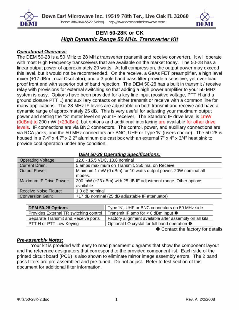
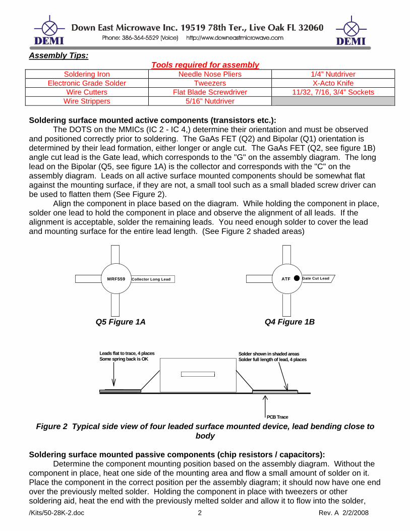
Soldering surface mounted active components (transistors etc.): The DOTS on the MMICs (IC 2 - IC 4,) determine their orientation and must be observed and positioned correctly prior to soldering. The GaAs FET (Q2) and Bipolar (Q1) orientation is determined by their lead formation, either longer or angle cut. The GaAs FET (Q2, see figure 1B) angle cut lead is the Gate lead, which corresponds to the "G" on the assembly diagram. The long lead on the Bipolar (Q5, see figure 1A) is the collector and corresponds with the "C" on the assembly diagram. Leads on all active surface mounted components should be somewhat flat against the mounting surface, if they are not, a small tool such as a small bladed screw driver can be used to flatten them (See Figure 2). Align the component in place based on the diagram. While holding the component in place, solder one lead to hold the component in place and observe the alignment of all leads. If the alignment is acceptable, solder the remaining leads. You need enough solder to cover the lead and mounting surface for the entire lead length. (See Figure 2 shaded areas)
MRF559 Collector Long Lead
ATF Gate Cut Lead
Q5 Figure 1A Q4 Figure 1B
PCB Trace
Leads flat to trace, 4 places Some spring back is OK
Solder shown in shaded areas Solder full length of lead, 4 places
Figure 2 Typical side view of four leaded surface mounted device, lead bending close to
body
Soldering surface mounted passive components (chip resistors / capacitors): Determine the component mounting position based on the assembly diagram. Without the component in place, heat one side of the mounting area and flow a small amount of solder on it. Place the component in the correct position per the assembly diagram; it should now have one end over the previously melted solder. Holding the component in place with tweezers or other soldering aid, heat the end with the previously melted solder and allow it to flow into the solder,

/Kits/50-28K-2.doc 3 Rev. A 2/2/2008
remove the iron and once solidified, remove holding tool. Now heat and flow the solder to the other side of the component and your done! Soldering leaded components (resistors, capacitors, diodes, etc.): Depending on your available tools, you can solder your transverter's components from either the top or bottom of the PCB. It is suggested for the home assembler to use a method that is comfortable. A simple holding vise can be utilized to allow the components to be 'dropped in' from the top side and soldered on this side without flipping over the assembly. As an alternate method, you can insert one component at a time in the correct mounting location and gently push down to the circuit board, while holding the component, flip over the circuit board and bend the leads over in opposite direction to hold the component in place. Although this is the most reliable method, there are some drawbacks if the component must be removed when the PCB is installed in the box. Rework of soldered components if needed: The easiest method to rework soldered components is to employ a de-soldering braid that is specifically designed for this purpose. It can be purchased at any electronics store (Radio Shack P/N 64-2090). Place the de-soldering braid on the lead that you are removing and apply heat to it. Without excessive pressure, the solder will melt and flow into the braid leaving the lead or component ready to be removed. Suggested Assembly: The DEM 50-28K is fairly easy and fun to assemble even for the first time kit builder and can be completed in any order that is comfortable, however DEM Inc. suggests the following assembly procedure to minimize errors and possible frustration. The parts in this kit are conveniently packed in separate bags to allow for easy identification. Referring to the component list in the rear of the manual, take careful inventory of the parts of the kit. These bags have been carefully packed, however, should any parts be missing, please feel free to call the factory for replacements. Referring to the component placement bottom side view, you will see that there are three (3) surface mounted active components (2 MMICs, 1 transistor). The bottom assembly operation should begin by orienting the PCB with the bottom side assembly diagram. Orientation can be determined by observing the notches on the long sides of the PCB. The following assembly order is suggested: Observe polarity using either the DOTS or lead configuration as explained in the Assembly Tips section.
1. Fit Q1, (MRF559, 940P1, or 1359-1) in place on the mounting pads and do not allow the leads to bridge traces. Once fit, solder Q1 in place. 2. Install and solder the other active components IC 2 (MAR3) and IC 3 (MAV11).
The bottom side is complete, observed your soldering and component orientation one more time to ensure everything is correct! Top Side Suggested Assembly: The band pass filters on the top side assembly, indicated by the heavy black line, have been installed and pre-aligned. Do not adjust the trimmer capacitors unless you have access to the necessary equipment required for alignment. For the first step, it is recommended that all inductors should be formed prior to the start of assembly of the top side. The coils should be formed per the parts list. Winding toroid type inductors is not an exact science and you should not be intimidated by it. Using the supplied wire, extend about ¼" through the indicated toroid and wind the wire around it, counting each revolution as one turn. When the total number of turns is

completed per the component list, cut the wire an additional ¼" beyond the toroid. Form the two ¼" leads so they are pointing in the same direction, (down from the toroid) and be sure to space the windings evenly. To ensure a positive solder connection, the ¼" leads should have the enamel insulation removed prior to soldering. This can be accomplished by applying solder to a hot soldering iron tip and placing the lead in the molten solder, you will see the insulation bubble indicating that it has melted. The tinned lead should be a silver color indicating that the insulation has been removed and the solder has tinned the base metal. Remove any excess solder from the leads so they will fit into the PC board holes during installation.
/Kits/50-28K-2.doc 4 Rev. A 2/2/2008
The top side assembly operation should begin by orienting the PCB with the top side assembly diagram. Orientation can be determined by observing the notches on the long sides of the PCB. You will notice on the assembly diagram that there are circles shown which will provide locating help when installing components. These have the following meaning:
Large Double Circles = Mounting Holes Small Double Circles = Wire Connections Small circles are component mounting holes
First, after reviewing the surface mounted passive component assembly tips, install C29, 0.1μF chip, C30, 0.1μF chip, R7, 24 ohm chip, R8, 24 ohm chip, C31, 1000pf chip, and C26, 1000pf chip. These are the surface mount components around Q2. Install C7, C9 & C10. These are surface mounted 0.1μF chip capacitors located on the left side of the PCB near the hybrid power module. Now install C28 and C27. Be sure to pick the 2 surface mount trimmer capacitors that are in Bag 2 (flat leads). Now install L11, R9, 100 ohm 1/2W, and R6, 1K ohm next. These components need a little extra forming. One lead of each needs to be surface mounted. Simply bend one of the leads of L11 out and place the other lead in a ground via hole. You may need to "trim to fit" the surface mount lead. Keep the connection as short as possible and the coil as close to the PCB as possible. Solder into place. R6 and R9 are formed by bending one lead in a right angle and placing this lead in the proper via hole, see Figure 9. "Trim to fit" the other lead to the transmission line keeping the leads as short as possible and the body of these components as close to the PCB as possible. Next, install Q2 GaAs FET. Note its orientation and solder into place using the tips for soldering surface mount active components provided in the beginning of this document if required. All surface soldering is now complete. NOTE: By installing the GaAs FET last it should help protect it from static discharge damage as all of the support components will help decouple and protect it. Assemble and solder the rest of the components. We suggest to pick an area of the PC Board, then stuff and solder per the assembly diagram. Using a highlighter to color the assembly diagram and parts list as you go will help insure proper complete assembly. You may refer to the schematic as you move along for a detailed description and to gain an understanding of the circuit you are assembling. The only component that may not be installed is R16, 330 ohm. This is the bias resistor for the extra gain stage that is only required if you transceiver has less than 1 mW output. If you are not sure, please consult Down East Microwave or you owners manual for your transceiver. If you require the optional TX gain stage, (if your transceiver has +0dBm output or less), install IC4 (MAR6) now referring to the User Options in page 11, section 2. Also, install R16. After completing the component assembly, install the hook-up wires. Install and solder wires in the shown areas on the board indicated by small double circles. The approximate sizes are shown in the table below All wiring is to be done on the top side of the circuit board only!! Strip ≈ ¼" from each end and solder, tin the end prior to installing the wires. Note: Flying Leads are wires that will be connected later in the assembly process.
WIRE CUT CHART

/Kits/50-28K-2.doc 5 Rev. A 2/2/2008
WIRE FROM TO SIZE #26 Teflon TXON TXON 6" #26 Teflon RXON RXON 2" #26 Teflon TR TR 2" #26 Teflon +13.8 SW near R28 +13.8 SW near CR 2 5" #26 Teflon TXLED Flying Lead 2½" #26 Teflon +13.8 SW near CR 1 +13.8 SW near CR 2 2" #26 Teflon +13.8 near L5 Flying lead 3" #26 Teflon TTL or PTT Flying lead 2½" #26 Teflon SWLED Flying lead 2½" #26 Teflon +13.8 SW Flying lead 4" #22 Teflon RXIF Flying Lead 1½" #22 Teflon TXIF Flying Lead 1¼" #26 Teflon NO or NC Flying Lead 3” #26 Teflon C Flying Lead 3”
Post soldering, all lead and wires protruding through the PCB on the bottom side, should be trimmed as short as possible to eliminate possible shorting to the external box when installed. Look over your work for solder bridging to adjacent traces, incorrectly installed components, etc. The printed circuit board is now complete. Take some time and review your assembly to this point re-checking the component location, installation, and polarity. PCB assembly into the external box: The heat sink and box are pre-drilled at the factory for your convenience. Notice that the heat sink, box and the circuit board have corresponding holes that are directional and must be aligned correctly. The heat sink and the box are attached with a common screw / nut combination. Installation in the box is easy if the suggested assembly steps are followed. If not already done, remove the cover from the box and wipe the inside clean to remove any remaining metal particles that may have been trapped during drilling. Spread a thin film of Thermal Compound between the 2 tapped (threaded) holes in the heatsink. Aligning the box and heat sink pre drilled holes, mount the heat sink to the box. Place one cap screw in a pre-drilled hole from the "fin" side of the heat sink. While holding the screw in the heat sink with the provided Allen Key wrench, start a 4-40 nut on the screw threads inside of the box and hand tighten only. Install one more screw in a diagonal location from the last screw and hand tighten only. Install the balance of the screws from the 'fin' side of the heat sink and install all of the nuts and tighten.
Thermal Compound Radio Shack P/N 276-1372 Install all of the rear wall mounted connectors per Figure 4.
2 - BNC connectors at the RX and TX positions using the supplied 3/8" nuts. If washers are supplied, install them on the inside of the box. If you have difficulty tightening the connector, connect an adapter or cable connector and hold this while tightening to keep it from spinning. 1 - BNC connector at the XMIT RF position as before but under the nut place the 3/8" solder lug. Bend the lug away from the wall to form right angle. 3 - RCA connectors for auxiliary, control and 13.8 VDC using the supplied hardware. The flat washer should be installed on the outside of the box and the solder lug should be installed on the inside. Post tightening, the lug should be bent away from the wall. 1 - Type “N” or UHF connector, user choice. Installed with lock washer and ground lug. Position lug toward rib on inner wall.

/Kits/50-28K-2.doc 6 Rev. A 2/2/2008
IF
XMIT RECEIVE13.8 VDC TX RX
<---------------------- HEAT SINK ----------------------->
CONTROL AUX
RF
Figure 4 Jack Mounting Positions Outside View
Place the finished circuit board over the eight 4-40 screws and gently push flat against the nuts. Place two nuts on opposite corners on the screws extending through the PCB and tighten evenly. Now mount the switch in the hole labeled "POWER" using the supplied hardware. Note the switch toggle position as shown in figure 5. At this point, some of the flying wires will need to be connected in the box to allow preliminary electrical testing as follows: Connect the #26 Teflon (TTL or PTT) wire to the wall mounted RCA Control jack, then install a 1000 pF capacitor between the center pin and solder lug and solder. (See Figure 4 for jack location).
Connect and solder (a 3” #18 Teflon wire) from the wall mounted DC POWER jack to the pad marked +13.8V near L5. Install the 100uf 25VDC electrolytic capacitor between the center pin and solder lug on the 13.8 VDC RCA jack and solder. Connect the #26 wire from this same center pin to the center terminal of the Power Switch. Connect the #26 Teflon wire from +13.8SW near R28 to the top terminal on the wall mounted switch. The top terminal will be closest one to you looking in the cavity of the box. Connect and solder a 1000 ρF capacitor from the center pin to the solder lug of the AUX RCA jack. If you will not be using the AUX port, go to the next paragraph. Otherwise, connect the #26 Teflon wire from “C” to the same AUX jack solder lug. Then connect the #26 Teflon wire from “NC” or “NO” to the center pin of the AUX jack. The AUX jack can then be used to hard key an external power amplifier.
POWER ON XMIT
Switch Toggle Direction
<---------------------------- HEAT SINK ----------------------->
Figure 5 Switch / LED Mounting Positions
Electrical Test Verification: The following information is provided to electrically pretest the transverter prior to final assembly. If you have a frequency counter it would be helpful but is not mandatory. Apply 13.8 volts to the RCA DC Power jack. The center pin is positive. Turn on the power switch, the transverter will now be in the receive mode. Check the voltages in the order shown. The Die cast box is ground.

/Kits/50-28K-2.doc 7 Rev. A 2/2/2008
MODE LOCATION VOLTAGE reference to Ground RX RXON 13.8 VDC ±0.5 RX Junction of C31 & R9 3.0 VDC +0.5 RX Junction of R10 & C35 7.0± 1 VDC RX Junction of R24 & C63 2.2 VDC± 0.5 RX C55 and M1 Frequency check, 22.000 MHz. Adjust C62
The voltage check list below is for the transverter in the TX mode. To place the transverter into the TX mode either apply 1 to 15 volts to the TTL input or ground the PTT line. The choice is made by you depending on your transceiver. The voltages may differ if tested with RF applied.
MODE LOCATION VOLTAGE (Reference to Ground unless Specified)
TX Relay K1 Audible Click TX Relay K2 Audible Click TX TXON 13.8 VDC ±0.5 TX TXLED 13.8 VDC±0.5 TX Junction of R3 & C23 5.0 VDC±0.5 TX Junction of C23 & R2 0.7±0.1 VDC TX Across R1 1.0 Volt Drop±0.2 VDC TX Output of VR 3 9.0 VDC±0.5 TX Anode of CR 5 1.5 VDC±0.5 TX Cathode of CR 4 0.7 VDC±0.5 TX Junction of R16 & C52 3.5 VDC± 0.5 only if IC 4 is Installed
*** DO NOT PROCEED UNTIL THE ABOVE CHECK POINTS ARE VERIFIED *** Once check points are verified, install the remaining six 4-40 nuts on the screws holding the PCB.
Power Module Installation: Place the power module (IC 1) on the box floor in its mounting location and trim the leads so they do not extend past the mounting pads, they should be approximately 3/8" long once trimmed. Now remove the hybrid and wipe the mounting surfaces of the box floor and flange of IC 1. Verify the surfaces are free of any foreign matter before applying a thin even coating of thermal compound to the mounting flange. Place IC 1 on the box floor while lining up the leads with the traces of the circuit board. Install two 6-32 x 3/8" screws through the mounting flange into the box floor and tighten evenly. NOTE: Make sure IC 1 is mechanically sound to the bottom of the enclosure. Improper seating of the hybrid could result in poor grounding and heat transfer causing damage to the power module. Form the leads flat to the traces and solder all leads of IC 1 to the circuit board. Caution: Solder leads only after module is securely fastened in place. Do not attempt to tighten screws after the leads are soldered as mechanical shifting may damage the module. LED Installation: The longer lead on the LED is positive. Prepare both LED's by supporting the SHORT lead (negative) at the LED body, bend the lead 90º away from the longer lead. Place the "ON" LED in the wall mounting hole (see Figure 5) and place the previously formed lead in the plated through hole closest to the edge of the board and solder. Repeat this process for the "XMIT" LED placing the formed lead in the closest plated through hole and solder. Cut the positive lead of the "XMIT" LED to approximately 3/8 Form a "J" in the lead by bending with pliers. Connect the #26 Teflon wire from the hole in the PCB near filter F4 labeled TXLED, to the "J" formed positive lead on the
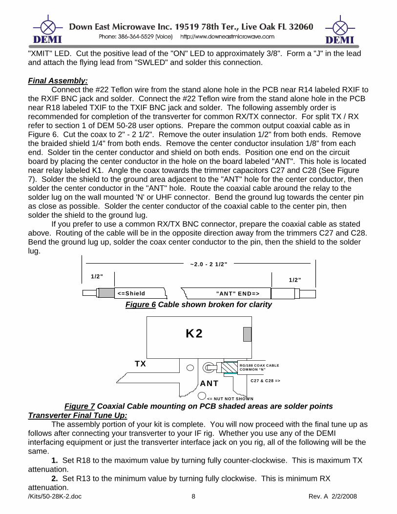
"XMIT" LED. Cut the positive lead of the "ON" LED to approximately 3/8". Form a "J" in the lead and attach the flying lead from "SWLED" and solder this connection. Final Assembly: Connect the #22 Teflon wire from the stand alone hole in the PCB near R14 labeled RXIF to the RXIF BNC jack and solder. Connect the #22 Teflon wire from the stand alone hole in the PCB near R18 labeled TXIF to the TXIF BNC jack and solder. The following assembly order is recommended for completion of the transverter for common RX/TX connector. For split TX / RX refer to section 1 of DEM 50-28 user options. Prepare the common output coaxial cable as in Figure 6. Cut the coax to 2" - 2 1/2". Remove the outer insulation 1/2" from both ends. Remove the braided shield 1/4" from both ends. Remove the center conductor insulation 1/8” from each end. Solder tin the center conductor and shield on both ends. Position one end on the circuit board by placing the center conductor in the hole on the board labeled "ANT". This hole is located near relay labeled K1. Angle the coax towards the trimmer capacitors C27 and C28 (See Figure 7). Solder the shield to the ground area adjacent to the "ANT" hole for the center conductor, then solder the center conductor in the "ANT" hole. Route the coaxial cable around the relay to the solder lug on the wall mounted 'N' or UHF connector. Bend the ground lug towards the center pin as close as possible. Solder the center conductor of the coaxial cable to the center pin, then solder the shield to the ground lug. If you prefer to use a common RX/TX BNC connector, prepare the coaxial cable as stated above. Routing of the cable will be in the opposite direction away from the trimmers C27 and C28. Bend the ground lug up, solder the coax center conductor to the pin, then the shield to the solder lug.
~2.0 - 2 1/2"
1/2" 1/2"
<=Shield "ANT" END=> Figure 6 Cable shown broken for clarity
TX
ANT
K2
RG/188 COAX CABLE COM M ON “N”
<= NUT NOT SHOW N
C27 & C28 =>
Figure 7 Coaxial Cable mounting on PCB shaded areas are solder points
Transverter Final Tune Up: The assembly portion of your kit is complete. You will now proceed with the final tune up as follows after connecting your transverter to your IF rig. Whether you use any of the DEMI interfacing equipment or just the transverter interface jack on you rig, all of the following will be the same. 1. Set R18 to the maximum value by turning fully counter-clockwise. This is maximum TX attenuation.
/Kits/50-28K-2.doc 8 Rev. A 2/2/2008
2. Set R13 to the minimum value by turning fully clockwise. This is minimum RX attenuation.

3. Connect the DEM 50-28 to your transceiver. (Consult your transceiver's manual or the document of any DEMI transverter interface circuit for connection details). Set the frequency of the transceiver for the weak signal portion of the band. (28.100 to 28.200 MHz.)
/Kits/50-28K-2.doc 9 Rev. A 2/2/2008
4. Turn on the power switch to apply power to the transverter. The power LED should light and the transmit LED should be extinguished. 5. Place an antenna or signal generator on the RF connector and adjust C27 and C28 for maximum receiver signal strength in the IF receiver. Minimum noise figure and maximum gain occur at nearly the same point so tune for maximum signal strength. If a signal generator or "On the Air" signal is not available, a 50 ohm coaxial termination maybe connected to the RF connector and adjust C27 and C28 for maximum noise in the IF receiver. Note: If the receiver is to be aligned on a noise figure meter, L11 can be "tweaked" in conjunction with C27 and C28 for desired noise figure and gain. 6. The resting “S” meter position can now be set by adjusting R13. This control adjusts the 28 MHz RX IF output signal. Adjust for minimal change when powering transverter on and off. 7. Connect a power meter or in-line forward SWR meter that is rated for 25 watts or more output power at 50 MHz. to the antenna jack of the transverter (or TX jack) 8. After verifying that the IF transmitter signal level being used is below 200 mW, change the transceiver to the CW position with the carrier level set to minimum. 9. Switch the transceiver into the transmit mode. While observing the power meter slowly increase the carrier control to the maximum setting or when the power output reaches 20 watts. 10. If the carrier control is at the maximum and the power output is below 20 watts, slowly turn R18 clockwise which will increasing the output power. Stop adjusting at 20 watts. Proceed to step 12. If 20 watts can not be obtained with less than 200 mW of IF drive, then re-check all TX voltages and connections. If nothing wrong is found, proceed to step 11. 11. Measure the current drain of the transverter while making a brief transmission. If it exceeds 4 amps with less than 20 watts out, check the TR switch for functioning or the low-pass filter for correct values. (L1-L4, C1-C4, C8) Be sure that the windings on toroids L1-L4 are spaced evenly. If current drain is not up to spec, it means that the transverter is either under driven with TXIF power or the TX gain stages between the mixer and the Hybrid power module are not amplifying. Recheck all voltages. If needed, power output can be measured at the input of the Hybrid. 100 mW is nominal. If this cannot be achieved, it is possible that one of the pre-built filter is out of tune. They can be tweaked for power out. If you have installed the optional TXIF gain stage, recheck the voltage test point and its proper installation. If difficulty still occurs, contact DEMI for help. 12. If you have a frequency meter, set the LO frequency and close the transverter with the cover. 13. Attach the 3/8" adhesive backed rubber feet to the cover. 14. Attach the supplied jack / switch labels to the box by first cleaning the mounting surface with a multi-purpose household surface cleaner. Use figure 4 and 5 for placement location. If you need external switching for relays or power amplifiers this can be accomplished via Relay K1 and the RCA Auxiliary connector. Consult the DEM 50-28 supplied schematic for switching details.
DEM 50- 28 User Options:
1. Split RX / TX connectors To operate with split TX / RX connectors it is necessary to perform the following modification. It is recommended by DEM that the 'N' or UHF connector be used on the receive side: 1. Remove capacitor C26. It is located near C27 trimmer capacitor.

/Kits/50-28K-2.doc 10 Rev. A 2/2/2008
2. Prepare two pieces of RG/188 coax as shown in Figure 6 of the DEM assembly documents. 3. Attachment to the circuit board will be per the figure below.
4. Route the RX cable to the N or UHF connector. Bent the solder lug towards the center pin as close as possible. Solder the center conductor to the pin and the shield to the ground.
5. Route the TX cable to the BNC connector and solder the center conductor to the pin of the connector. Then, solder the shield to the solder lug installed on the connector.
TX
ANT
K2 RG/188 COAX CABLE
<= NUT NOT SHOWN
RX
TO UHF or N connector
TO BNC
1/2" END
1/2" END C27
R6
2. Optional Gain Stage You have the option of installing an additional gain stage in the transmit section of the transverter. Note: All transceivers do not require this additional stage, please consult Down East Microwave Inc. factory if these options have not been already considered. If you elect to install this gain stage, a modification must be performed to the printed circuit board prior to continuing. Referring to the diagram below and the assembly document, remove the "Ribs" by cutting at the two indicated points with a sharp razor blade and heating with a soldering iron to remove. Proceed to install MMIC using the procedures outlined previously.
Remove all Ribs Prior to IC4 Installation

/Kits/50-28K-2.doc 11 Rev. A 2/2/2008
DEM 50-28K Component List BAG 1 CONTENTS: Resistor (R) values are leaded 1/4W unless otherwise specified. Color code for resistors is given below disregarding the last band (GOLD) for 5% tolerance. Capacitors (C) are chips and the values are picoFarads unless otherwise specified. All chips are in Bag 1.
BAG 1 R1 15 BRN,GRN,BLK R11 47 YEL,VIO,BLK R21 39 ORG,WHT,BLK C10 0.1μF CHIP R2 1.5K BRN,GRN,RED R12 220 RED,RED,BRN R22 150 BRN, GRN,BRN C17 0.75 ρF CHIP R3 270 RED,VIO,BRN R13 1K POT (102) R23 330 ORG,ORG,BRN C26 1000 ρF CHIP R4 100 BRN,BLK, BRN R14 220 RED,RED,BRN R24 270 RED,VIO,BRN C29 0.1μF CHIP R5 330 ORG,ORG,BRN R15 1K BRN, BLK,RED R25 5.6K GRN,BLU,RED C30 0.1μF CHIP R6 1K BRN, BLK,RED R16 330 (OPT)
ORG,ORG,BRN R26 10K BRN, BLK,ORG C31 1000 ρF CHIP
R7 24 CHIP (240) R17 220 RED,RED,BRN R27 1K BRN, BLK,RED C38 0.75 ρF CHIP R8 24 CHIP (240) R18 1K POT (102) R28 1K BRN, BLK,RED C40 0.75 ρF CHIP R9 100 1/2W BRN, BLK,BRN R19 220 RED,RED,BRN C7 0.1μF CHIP R10 150 1/2W BRN, GRN,BRN
R20 150 BRN, GRN,BRN C9 0.1μF CHIP
= Pre-assembled on circuit board as part of filter.
BAG 2 CONTENTS: All capacitors are disc ceramic and the values are ρF unless otherwise specified. (xxx) Designates capacitor marking. “Trimmer” = variables. “TH”=Thru Hole
BAG 2 C1 68 (68) C21 1000 (102) C43 1000 (102) C59 120 (121) C2 120 (121) C22 0.1μF (104) C44 39 (39) C60 1000 (102) C3 120 (121) C23 1000 (102) C45 18 (18) C61 39 (39) C4 120 (121) C24 1000 (102) C46 120 (121) C62 2-12 Trimmer TH C5 2.2μF C25 1000 (102) C47 1000 (102) C63 56 (56) C6 2.2μF C27 2-12 Trimmer C48 270 (271) C64 18 (18) C8 68 (68) C28 2-12 Trimmer C49 1000 (102) C65 39 (39) C11 1000pF (102) C32 2.2μF C50 270 (271) C66 1000 (102) C12 1000pF (102) C33 1000 (102) C51 1000 (102) C67 1000 (102) C13 2.2μF C34 2.2μF C52 1000 (102) C68 2.2μF C14 2.2μF C35 1000 (102) C53 0.1μF (104) C69 2.2μF C15 1000 (102) C36 0.1μF (104) C54 1000 (102) C70 0.1μF (104) C16 2-12 Trimmer C37 2-12 Trimmer C55 1000 (102) C71 0.1μF (104) C18 2-12 Trimmer C39 2-12 Trimmer C56 1000 (102) C19 1000 (102) C41 2-12 Trimmer C57 120 (121) C20 0.1μF (104) C42 1000 (102) C58 270 (271)
= Pre-assembled on circuit board as part of filter.
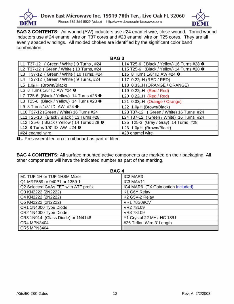
BAG 3 CONTENTS: Air wound (AW) inductors use #24 enamel wire, close wound. Toriod wound inductors use # 24 enamel wire on T37 cores and #28 enamel wire on T25 cores. They are all evenly spaced windings. All molded chokes are identified by the significant color band combination.
/Kits/50-28K-2.doc 12 Rev. A 2/2/2008
BAG 3
L1 T37-12 ( Green / White ) 9 Turns , #24 L14 T25-6 ( Black / Yellow) 16 Turns #28 L2 T37-12 ( Green / White ) 10 Turns, #24 L15 T25-6 (Black / Yellow) 14 Turns #28 L3 T37-12 ( Green / White ) 10 Turns, #24 L16 8 Turns 1/8” ID AW #24 L4 T37-12 ( Green / White ) 9 Turns, #24 L17 0.22μH (RED / RED) L5 1.0μH (Brown/Black) L18 0.33μH (ORANGE / ORANGE) L6 8 Turns 1/8” ID AW #24 L19 0.22μH (Red / Red) L7 T25-6 (Black / Yellow) 14 Turns #28 L20 0.22μH (Red / Red) L8 T25-6 (Black / Yellow) 14 Turns #28 L21 0.33μH (Orange / Orange) L9 8 Turns 1/8” ID AW #24 L22 1.0μH (Brown/Black) L10 T37-12 (Green / White) 16 Turns #24 L23 T37-12 ( Green / White) 16 Turns #24 L11 T25-10 (Black / Black ) 13 Turns #28 L24 T37-12 ( Green / White) 16 Turns #24 L12 T25-6 ( Black / Yellow ) 14 Turns #28 L25 T25-3 (Gray / Gray) 14 Turns #28 L13 8 Turns 1/8” ID AW #24 L26 1.0μH (Brown/Black) #24 enamel wire #28 enamel wire = Pre-assembled on circuit board as part of filter.
BAG 4 CONTENTS: All surface mounted active components are marked on their packaging. All other components will have the indicated number as part of the marking.
BAG 4
M1 TUF-1H or TUF-1HSM Mixer IC2 MAR3 Q1 MRF559 or 940P1 or 1359-1 IC3 MAV11 Q2 Selected GaAs FET with ATF prefix IC4 MAR6 (TX Gain option Included) Q3 KN2222 (2N2222) K1 G6Y Relay Q4 KN2222 (2N2222) K2 G5V-2 Relay Q5 KN2222 (2N2222) VR1 78S09CV CR1 1N4000 Type Diode VR2 78L09 CR2 1N4000 Type Diode VR3 78L09 CR3 1N914 (Glass Diode) or 1N4148 Y1 Crystal 22 MHz HC 18/U CR4 MPN3404 #26 Teflon Wire 3' Length CR5 MPN3404

/Kits/50-28K-2.doc 13 Rev. A 2/2/2008
HARDWARE KIT (2) 1000pF Capacitor #22 Teflon Wire 4" (1) 100 uF Capacitor #18 Teflon Wire 4" (2) LED, RED RG/188U Mini Coax 6" (1) SW1 Power Switch (1) Hammond 1590D Box (3) BNC Female UG1094/U Connectors (1) "N" connector and hardware (3) RCA Jacks - Control, Aux., Power (1) 5" x 7" Heatsink (1) 3/8" Solder lug for BNC connector (1) Label, Front "XMIT, ON, POWER" (11) 4-40 x 5/8" Cap Screws (1) Label, Rear "13.8 VDC, XMIT RF RECEIVE" (22) 4-40 Nuts (1) Label, Rear "CONTROL, AUX, RX IF TX" (2) 6-32 x 3/8" Pan Machine Screws for Power Module (4) Adhesive Backed Rubber Feet (1) UHF connector and hardware (1) Type “N” connector (optional) Miscellaneous Loose Parts and Pin configurations: 1. RF Power Module IC1, M57735 2. Printed Circuit Board
Cathode
MPN3404 diode
This end soldered to PCB surface
Circuit Board Surface
Fig. 8 Fig. 9

/Kits/50-28K-2.doc 14 Rev. A 2/2/2008
50-28 Common IF Input Circuit Option This option is used for common IF input for the 50-28 transverter. There are two versions of this option. It is a pin switch designed for High and Low Power. The Low Power version is used with a transceiver that has a single transverter port. Most of these types of transceivers do require the extra gain stage (TXIF) to be installed in the transverter to increase the 28 MHz output level of the transceiver. This option should not be used if drive level is over 1mW. The High Power version should be used with transceivers that have up to 10 Watts of output. It has a 50 ohm termination mounted on the case for power dissipation. There are two parts lists for each version. The components designators are the same for both and only the parts required for the pin switches are listed. Assemble after the transverter PC board is completed using the component placement diagram.
Components Parts List - Add to Standard PCB Parts Placement Diagram
Low Power Option
For transceivers with 250mW or less drive. C85 1000pF C89 1000pF CR8 MPN3404 C86 1000pF C90 100pF CR9 MPN3404 C87 1000pF C95 1000pF L36 1.0 μH C88 100pF R37 1KΩ L37 10T #28 T25-10
High Power Option
For transceivers with greater than 250mW but not to exceed 10 Watts of drive. C85 1-6pF Trimmer C89 1000pF CR8 MA4P1200 C86 1000pF C90 100pF CR9 MA4P1200 C87 1000pF C95 1000pF L36 1.0 μH C88 100pF R37 150Ω 1W L37 10T #28 T25-10 R 50 ohm stud
1. Assemble version required by installing components on PCB per component placement diagram. Do not install C95 or 50 ohm stud.
2. Test Transverter PCB per instructions and add the following:
Junction of R37 and C86: 0 volts on Receive 1.5volts +/- .5 volts on Transmit
3. Install C95 to common IF input connector (labeled RXIF on standard installation) and solder to position on PC Board.
Grounded to case
PC Board
4. Install 50 ohm stud and solder tab to circuit board
if using High Power version.
5. Set C85 trimmer in the high power version to minimum (see page 10 of the assembly document). Proceed to test.