demo manual dc1414b-b ltm4601ahv 5vin to 28vin, …
TRANSCRIPT

1dc1414b-bf
DEMO MANUAL DC1414B-B
DESCRIPTION
LTM4601AHV 5VIN to 28VIN, 12A Step-Down
µModule Regulator
Demonstrat ion circui t 1414B-B features the LTM®4601AHVEV, the high efficiency, high density switch mode step-down power module. The input voltage range is 5V to 28V with a jumper selectable output voltage from 0.6V to 5V. The rated load current is 12A, although derating is necessary for certain VIN, VOUT and thermal conditions. The PLLIN pin supports synchronizing the μModule® regulator to an external clock. The TRACK/SS pin allows the user to program output ramp-up and ramp-down rates which may coincidentally or ratiometrically
L, LT, LTC, LTM, μModule, Linear Technology and the Linear logo are registered trademarks of Linear Technology Corporation. All other trademarks are the property of their respective owners.
PERFORMANCE SUMMARY
BOARD PHOTO
track with another voltage rail. Output voltage margining of ±5% from the nominal value is available via the margin control pins MARG0 and MARG1. The LTM4601AHV data sheet must be read in conjunction with this demo manual prior to working on or modifying demo circuit DC1414B-B.
Design files for this circuit board are available at http://www.linear.com/demo
(TA = 25°C)
PARAMETER CONDITION VALUE
Input Voltage Range 5V to 28V
Output Voltage VOUT Jumper Selectable (Open for 0.6V) 1.2V, 1.5V, 1.8V, 2.5V, 3.3V, 5V
Maximum Continuous Output Current Derating is Necessary for Certain VIN, VOUT and Thermal Conditions
12A DC
Default Operating Frequency 850kHz
External Synchronous Clock Frequency Range Please Refer to Data Sheet for Minimum tON and tOFF Requirement.
600kHz to 1000kHz
Efficiency VIN = 12V, VOUT = 3.3V, IOUT = 12A 89.5%, See Figure 2
2dc1414b-bf
DEMO MANUAL DC1414B-B
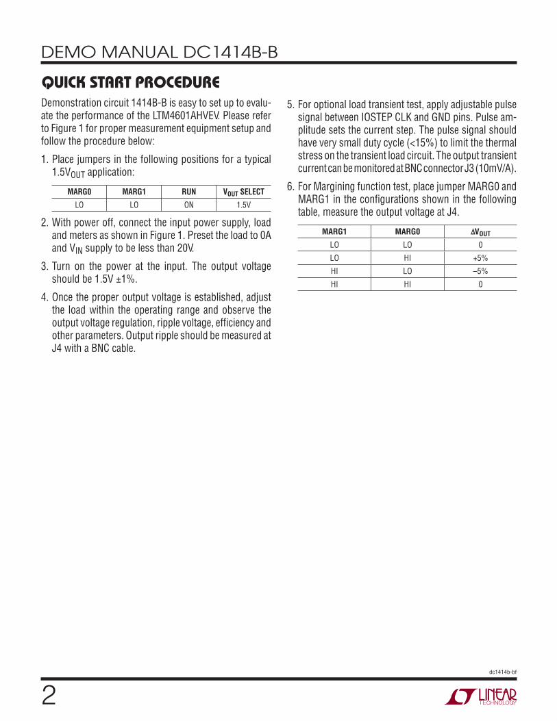
QUICK START PROCEDURE
Demonstration circuit 1414B-B is easy to set up to evalu-ate the performance of the LTM4601AHVEV. Please refer to Figure 1 for proper measurement equipment setup and follow the procedure below:
1. Place jumpers in the following positions for a typical 1.5VOUT application:
MARG0 MARG1 RUN VOUT SELECT
LO LO ON 1.5V
2. With power off, connect the input power supply, load and meters as shown in Figure 1. Preset the load to 0A and VIN supply to be less than 20V.
3. Turn on the power at the input. The output voltage should be 1.5V ±1%.
4. Once the proper output voltage is established, adjust the load within the operating range and observe the output voltage regulation, ripple voltage, efficiency and other parameters. Output ripple should be measured at J4 with a BNC cable.
5. For optional load transient test, apply adjustable pulse signal between IOSTEP CLK and GND pins. Pulse am-plitude sets the current step. The pulse signal should have very small duty cycle (<15%) to limit the thermal stress on the transient load circuit. The output transient current can be monitored at BNC connector J3 (10mV/A).
6. For Margining function test, place jumper MARG0 and MARG1 in the configurations shown in the following table, measure the output voltage at J4.
MARG1 MARG0 ΔVOUT
LO LO 0
LO HI +5%
HI LO –5%
HI HI 0
3dc1414b-bf
DEMO MANUAL DC1414B-B
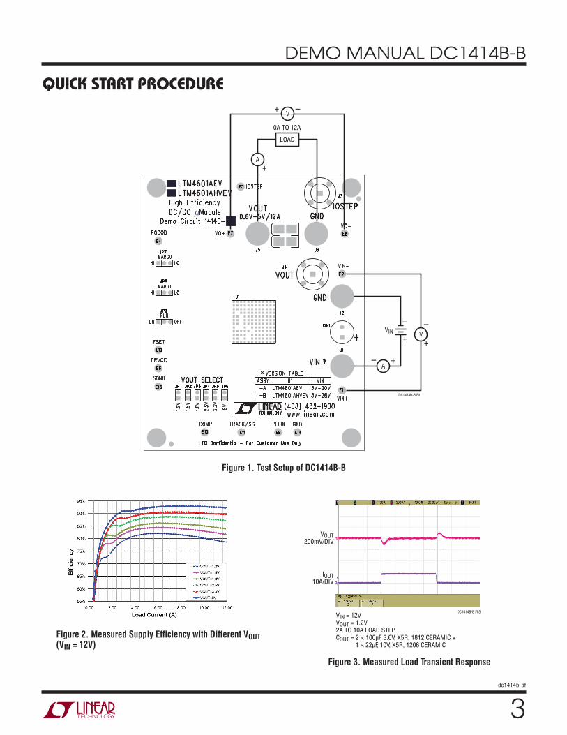
QUICK START PROCEDURE
Figure 1. Test Setup of DC1414B-B
Figure 2. Measured Supply Efficiency with Different VOUT (VIN = 12V)
Figure 3. Measured Load Transient Response
+
–
V+
–
A– +
A–
+
LOAD
0A TO 12A
V+ –
DC1414B-B F01
VIN
VIN = 12VVOUT = 1.2V2A TO 10A LOAD STEPCOUT = 2 100μF, 3.6V, X5R, 1812 CERAMIC + 1 22μF, 10V, X5R, 1206 CERAMIC
VOUT200mV/DIV
IOUT10A/DIV
DC1414B-B F03
4dc1414b-bf
DEMO MANUAL DC1414B-B
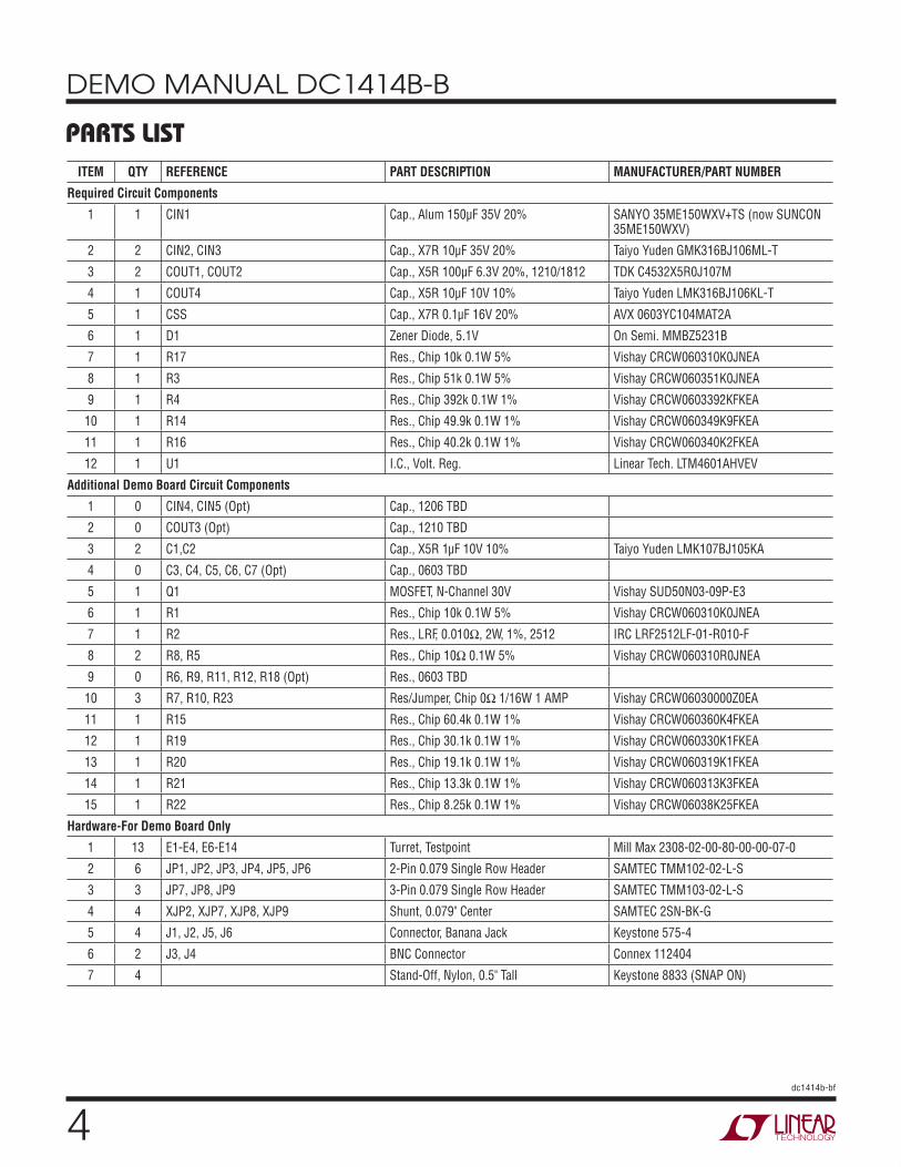
PARTS LIST
ITEM QTY REFERENCE PART DESCRIPTION MANUFACTURER/PART NUMBER
Required Circuit Components
1 1 CIN1 Cap., Alum 150μF 35V 20% SANYO 35ME150WXV+TS (now SUNCON 35ME150WXV)
2 2 CIN2, CIN3 Cap., X7R 10μF 35V 20% Taiyo Yuden GMK316BJ106ML-T
3 2 COUT1, COUT2 Cap., X5R 100μF 6.3V 20%, 1210/1812 TDK C4532X5R0J107M
4 1 COUT4 Cap., X5R 10μF 10V 10% Taiyo Yuden LMK316BJ106KL-T
5 1 CSS Cap., X7R 0.1μF 16V 20% AVX 0603YC104MAT2A
6 1 D1 Zener Diode, 5.1V On Semi. MMBZ5231B
7 1 R17 Res., Chip 10k 0.1W 5% Vishay CRCW060310K0JNEA
8 1 R3 Res., Chip 51k 0.1W 5% Vishay CRCW060351K0JNEA
9 1 R4 Res., Chip 392k 0.1W 1% Vishay CRCW0603392KFKEA
10 1 R14 Res., Chip 49.9k 0.1W 1% Vishay CRCW060349K9FKEA
11 1 R16 Res., Chip 40.2k 0.1W 1% Vishay CRCW060340K2FKEA
12 1 U1 I.C., Volt. Reg. Linear Tech. LTM4601AHVEV
Additional Demo Board Circuit Components
1 0 CIN4, CIN5 (Opt) Cap., 1206 TBD
2 0 COUT3 (Opt) Cap., 1210 TBD
3 2 C1,C2 Cap., X5R 1μF 10V 10% Taiyo Yuden LMK107BJ105KA
4 0 C3, C4, C5, C6, C7 (Opt) Cap., 0603 TBD
5 1 Q1 MOSFET, N-Channel 30V Vishay SUD50N03-09P-E3
6 1 R1 Res., Chip 10k 0.1W 5% Vishay CRCW060310K0JNEA
7 1 R2 Res., LRF, 0.010Ω, 2W, 1%, 2512 IRC LRF2512LF-01-R010-F
8 2 R8, R5 Res., Chip 10Ω 0.1W 5% Vishay CRCW060310R0JNEA
9 0 R6, R9, R11, R12, R18 (Opt) Res., 0603 TBD
10 3 R7, R10, R23 Res/Jumper, Chip 0Ω 1/16W 1 AMP Vishay CRCW06030000Z0EA
11 1 R15 Res., Chip 60.4k 0.1W 1% Vishay CRCW060360K4FKEA
12 1 R19 Res., Chip 30.1k 0.1W 1% Vishay CRCW060330K1FKEA
13 1 R20 Res., Chip 19.1k 0.1W 1% Vishay CRCW060319K1FKEA
14 1 R21 Res., Chip 13.3k 0.1W 1% Vishay CRCW060313K3FKEA
15 1 R22 Res., Chip 8.25k 0.1W 1% Vishay CRCW06038K25FKEA
Hardware-For Demo Board Only
1 13 E1-E4, E6-E14 Turret, Testpoint Mill Max 2308-02-00-80-00-00-07-0
2 6 JP1, JP2, JP3, JP4, JP5, JP6 2-Pin 0.079 Single Row Header SAMTEC TMM102-02-L-S
3 3 JP7, JP8, JP9 3-Pin 0.079 Single Row Header SAMTEC TMM103-02-L-S
4 4 XJP2, XJP7, XJP8, XJP9 Shunt, 0.079" Center SAMTEC 2SN-BK-G
5 4 J1, J2, J5, J6 Connector, Banana Jack Keystone 575-4
6 2 J3, J4 BNC Connector Connex 112404
7 4 Stand-Off, Nylon, 0.5" Tall Keystone 8833 (SNAP ON)
5dc1414b-bf
DEMO MANUAL DC1414B-B
Information furnished by Linear Technology Corporation is believed to be accurate and reliable. However, no responsibility is assumed for its use. Linear Technology Corporation makes no representa-tion that the interconnection of its circuits as described herein will not infringe on existing patent rights.
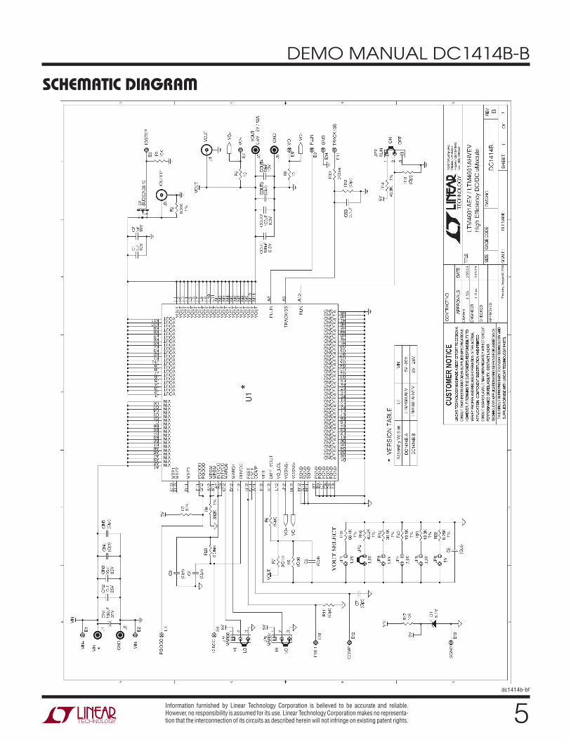
SCHEMATIC DIAGRAM

6dc1414b-bf
DEMO MANUAL DC1414B-B
Linear Technology Corporation1630 McCarthy Blvd., Milpitas, CA 95035-7417 (408) 432-1900 ● FAX: (408) 434-0507 ● www.linear.com © LINEAR TECHNOLOGY CORPORATION 2011
LT 0311 • PRINTED IN USA
DEMONSTRATION BOARD IMPORTANT NOTICE
Linear Technology Corporation (LTC) provides the enclosed product(s) under the following AS IS conditions:
This demonstration board (DEMO BOARD) kit being sold or provided by Linear Technology is intended for use for ENGINEERING DEVELOPMENT OR EVALUATION PURPOSES ONLY and is not provided by LTC for commercial use. As such, the DEMO BOARD herein may not be complete in terms of required design-, marketing-, and/or manufacturing-related protective considerations, including but not limited to product safety measures typically found in finished commercial goods. As a prototype, this product does not fall within the scope of the European Union directive on electromagnetic compatibility and therefore may or may not meet the technical requirements of the directive, or other regulations.
If this evaluation kit does not meet the specifications recited in the DEMO BOARD manual the kit may be returned within 30 days from the date of delivery for a full refund. THE FOREGOING WARRANTY IS THE EXCLUSIVE WARRANTY MADE BY THE SELLER TO BUYER AND IS IN LIEU OF ALL OTHER WARRANTIES, EXPRESSED, IMPLIED, OR STATUTORY, INCLUDING ANY WARRANTY OF MERCHANTABILITY OR FITNESS FOR ANY PARTICULAR PURPOSE. EXCEPT TO THE EXTENT OF THIS INDEMNITY, NEITHER PARTY SHALL BE LIABLE TO THE OTHER FOR ANY INDIRECT, SPECIAL, INCIDENTAL, OR CONSEQUENTIAL DAMAGES.
The user assumes all responsibility and liability for proper and safe handling of the goods. Further, the user releases LTC from all claims arising from the handling or use of the goods. Due to the open construction of the product, it is the user’s responsibility to take any and all appropriate precautions with regard to electrostatic discharge. Also be aware that the products herein may not be regulatory compliant or agency certified (FCC, UL, CE, etc.).
No License is granted under any patent right or other intellectual property whatsoever. LTC assumes no liability for applications assistance, customer product design, software performance, or infringement of patents or any other intellectual property rights of any kind.
LTC currently services a variety of customers for products around the world, and therefore this transaction is not exclusive.
Please read the DEMO BOARD manual prior to handling the product. Persons handling this product must have electronics training and observe good laboratory practice standards. Common sense is encouraged.
This notice contains important safety information about temperatures and voltages. For further safety concerns, please contact a LTC applica-tion engineer.
Mailing Address:
Linear Technology
1630 McCarthy Blvd.
Milpitas, CA 95035
Copyright © 2004, Linear Technology Corporation