department of electronics & communication engineering apps lab... · 2019-02-21 · list of...
TRANSCRIPT

Department of Electronics & Communication Engineering
Lab Manual
IC APPLICATIONS LAB
Prasad V. Potluri Siddhartha Institute of Technology
(Sponsored by: Siddhartha Academy of General& Technical Education)
Affiliated to JNTU- Kakinada
Approved by AICTE- New Delhi
Kanuru, Vijayawada-7
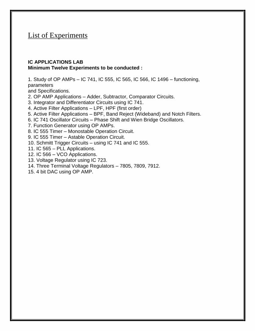
List of Experiments
IC APPLICATIONS LAB Minimum Twelve Experiments to be conducted : 1. Study of OP AMPs – IC 741, IC 555, IC 565, IC 566, IC 1496 – functioning, parameters and Specifications. 2. OP AMP Applications – Adder, Subtractor, Comparator Circuits. 3. Integrator and Differentiator Circuits using IC 741. 4. Active Filter Applications – LPF, HPF (first order) 5. Active Filter Applications – BPF, Band Reject (Wideband) and Notch Filters. 6. IC 741 Oscillator Circuits – Phase Shift and Wien Bridge Oscillators. 7. Function Generator using OP AMPs. 8. IC 555 Timer – Monostable Operation Circuit. 9. IC 555 Timer – Astable Operation Circuit. 10. Schmitt Trigger Circuits – using IC 741 and IC 555. 11. IC 565 – PLL Applications. 12. IC 566 – VCO Applications. 13. Voltage Regulator using IC 723. 14. Three Terminal Voltage Regulators – 7805, 7809, 7912. 15. 4 bit DAC using OP AMP.

2.OPAMPAPPLICATIONS- ADDER, SUBTRACTOR, COMPARATORCIRCUITS
AIM: Tostudy the applications of IC 741 as adder, subtractor, comparator.
APPARATUS: 1.IC 741
2.Resistors (1KΩ)—4
3.Function generator
4.Regulated power supply
5.IC bread board trainer
6.CRO
7.Patch cards and CRO probes
CIRCUIT
DIAGRAM: Adder:

Subtractor:

Comparator:
THEORY:
ADDER:
Op-Amp may beusedtodesignacircuit whose outputis the sum ofseveral input
signalssuchascircuitiscalledasummingamplifierorsummer.Wecanobtaineither inverting or non-
inverting summer.
Thecircuitdiagramsshowsatwoinputinvertingsummingamplifier.Ithastwo input voltages
V1andV2, two input resistors R1, R2and a feedback resistor Rf.
Assumingthatop-
ampisinidealconditionsandinputbiascurrentisassumedtobezero,thereisnovoltagedropacrosstheresis
torRcompandhencethenoninverting input terminal is atground potential.
Bytaking nodal equations.
V1/R1+V2/R2+V0/Rf=0
V0=-[(Rf/R1) V1+(Rf/R2) V2] And hereR1=R2=Rf=1KΩ V0=-(V1+V2)
Thus output is inverted and sum ofinput.

SUBTRACTOR:
Abasicdifferentialamplifiercanbeusedasasubtractor.Ithastwoinput signals V1and V2and
two inputresistances R1andR2 and afeedbackresistorRf.The input signals scaled to the desired
values by selecting appropriate values for the external resistors.
From the figure, the output voltage ofthe differential amplifier with a gain of‘1’ is
V0=-R/Rf(V2-V1)
V0=V1-V2.
Also R1=R2=Rf=1KΩ.
Thus,theoutputvoltageV0is equaltothevoltageV1appliedtothenoninverting terminal minus
voltage V2applied toinverting terminal.
Hence the circuit is sub tractor.
COMPARATOR:
Acomparator is a circuitwhich compares asignal voltage applied atoneinputofanop-
ampwithaknownreferencevoltageattheotherinput.Itisbasicallyanopen loop op-amp with output
±Vsatas in the ideal transfer characteristics.
ItisclearthatthechangeintheoutputstatetakesplacewithanincrementininputVi of
only2mv.Thisistheuncertaintyregionwhereoutputcannotbedirectly defined There are basically 2
types ofcomparators.
1. Non inverting comparator and.
2. Inverting comparator.
Theapplicationsofcomparatorarezerocrossingdetector ,windowdetector, time marker generator
and phase meter.
OBSERVATIONS:
ADDER:
V1(volts) V2(volts) Theoretical
V0=-(V1+V2)
Practical
V0 =-(V1+V2)

SUBTRACTOR:
V1(volts) V2(volts) Theoretical
V0=(V1-V2)
Practical
V0 =(V1-V2)
COMPARATOR:
Voltage input Vref Observed square wave amplitude
MODEL GRAPH:
PROCEDURE:
ADDER:
1.connections are made as per the circuit diagram.
2.Apply input voltage1) V1=5v,V2=2v
2) V1=5v,V2=5v 3) V1=5v,V2=7v.
3.Using Millimeter measure the dc output voltage atthe output terminal.
4.For different values ofV1and V2measure the output voltage.

SUBTRACTOR:
1.Connectionsaremade as per the circuit diagram.
2.Apply input voltage1) V1=5v,V2=2v
2) V1=5v,V2=5v 3) V1=5v,V2=7v.
3.Using multi meter measure the dc output voltage atthe output terminal. 4.For different values ofV1and V2measure the output voltage.
COMPARATOR:
1.Connections are made as per the circuit diagram.
2.Select the sine wave of10V peak topeak ,1K Hz frequency.
3.Apply the reference voltage 2V and trace the input and output wave forms.
4. Superimpose inputand output waveforms and measure sine wave amplitude
withreferencetoVref.
5.Repeatsteps3and 4with referencevoltagesas2V,4V,-2V,-4Vandobserve the waveforms.
6.Replace sine wave input with 5V dc voltage and Vref=0V.
7.Observe dc voltage atoutput using CRO. 8.Slowly increase Vrefvoltage and observe the change in saturation voltage.
PRECAUTIONS:
1.Make null adjustment before applying the input signal.
2.Maintain proper Vcclevels.
RESULT:

3.OP-AMP741ASDIFFRENTIATORANDINTEGRATOR
AIM:
Todesignandtestanop-ampdifferentiatorandintegrator
EQUIPMENTSANDCOMPONENTS:
APPARATUS
1. DC power supply
2. CRO
- 1 No.
-
1 No.
3. BreadBoard - 1 No.
4. FunctionGenerator- 1 No.
COMPONENTS:
1. 15 kΩ Resistor– 2 No.
2. 820 Resistor– 1 No.
3. 1.5 kΩ Resistor– 1 No.
4 0.01 F Capacitor– 2 No
5 0.5 nF Capacitor– 1 No
5 IC741 - 1 No.
THEORY Theoperationalamplifiercaneusedinmanyapplications. Itcanbeusedas
differentiatorandintegrator.Indifferentiatorthecircuitperformsthemathematical
operationofdifferentiation thatistheoutputwaveformisthederivativeoftheinput
waveformforgooddifferentiation, onemustensurethathetimeperiodoftheinput signal is
larger than or equal to RfC1.the practical differentiatoreliminates the problemof
instabilityandhighfrequencynoise.
CIRCUITDIAGRAM:

a
a
PROCEDURE:
1connectthedifferentiatorcircuitasshowninfig1.adjustthesignalgeneratorto producea5
voltpeaksinewaveat100 Hz.
2observeinputViandVosimultaneouslyontheoscilloscopemeasureandrecordthe
peakvalueofVo andthephaseangleofVowithrespecttoVi.
3.Repeatstep2whileincreasingthe frequencyofthe inputsignal.Find the maximum
frequencyatwhichcircuit offersdifferentiation.Compareitwiththecalculatedvalue of fa
Observe&sketchtheinputandoutputfor squarewave.
4.Connecttheintegratorcircuit showninFig2.Setthefunctiongeneratortoproduce
asquarewaveof1Vpeak-to-peakamplitudeat500Hz.Viewsimultaneouslyoutput VoandVi.
5.Slowlyadjusttheinputfrequencyuntiltheoutputisgoodtriangularwaveform.
Measuretheamplitudeandfrequencyof theinputandoutputwaveforms.
6.Verifythefollowingrelationship betweenR1Cfandinputfrequencyforgood
integrationf>fa&T<R1C1
WhereR1Cfisthetimeconstant
7.Nowsetthefunctiongeneratortoasinewaveof1Vpeak-to-peakandfrequency
500Hz. Adjustthefrequencyoftheinputuntiltheoutputisanegativegoingcosine
wave.Measurethefrequencyandamplitudeof theinputandoutputwaveforms.
OBSERVATIONS:
1. Thetimeperiodandamplitudeof theoutputwaveformof differentiatorcircuit
2. Thetimeperiodandamplitudeof theintegratorwaveform
CALCULATIONS: Design adifferentiatortodifferentiateaninputsignalthatvariesinfrequencyfrom10
Hz to 1 kHz.
f 1
2RfC1
fa=1 kHz, thehighestfrequencyof theinputsignal
LetC1=0.01 F,
ThenRf=15.9 k
ThereforechooseRf=15.0 k
f 1
2R1C1
Choose:fb=20x fa=20 KHz
HenceR1=795
ThereforechooseR1=820
SinceR1C1=RfCf(compensatedattenuator)
Cf=0.54 nF
ThereforechooseCf=0.5nF
Integrator:Designanintegratorthatintegratesasignalwhose frequenciesare
between1 KHz and10 KHz
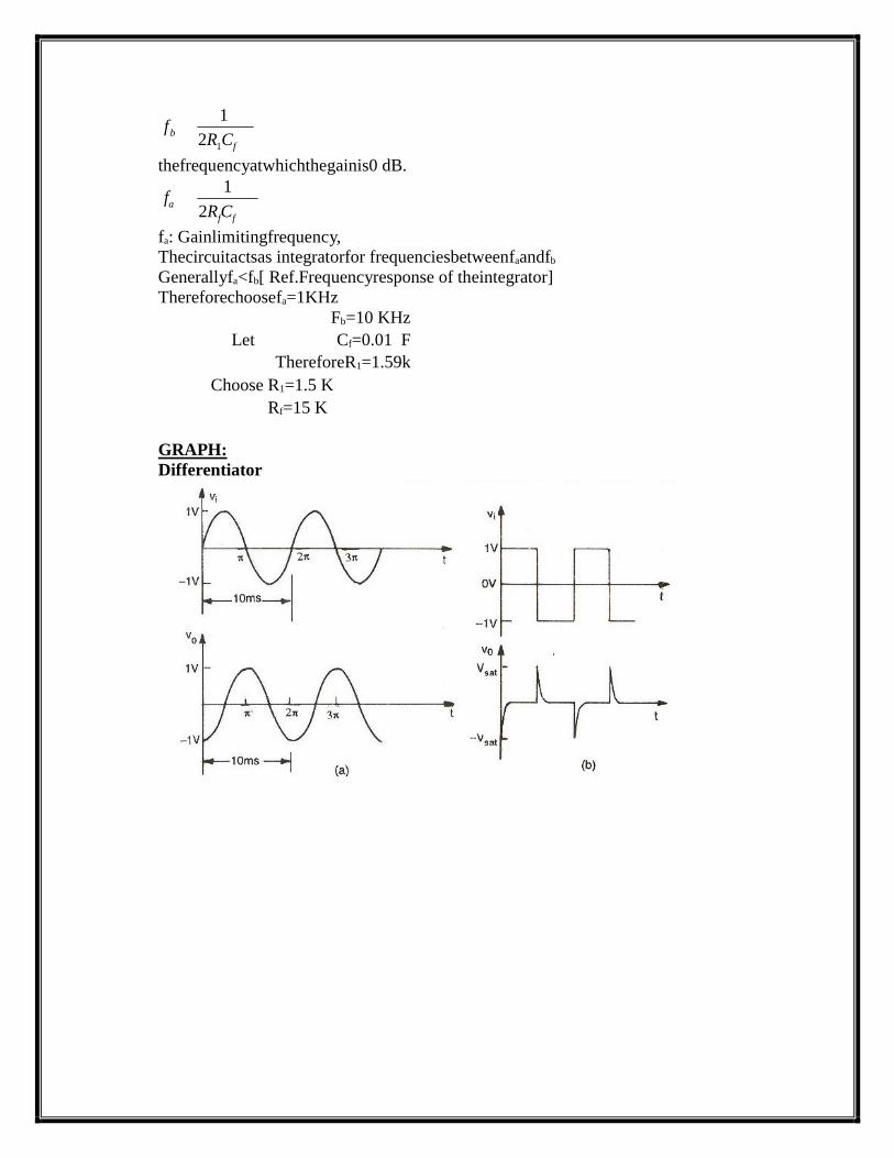
b
f 1
2R1Cf
thefrequencyatwhichthegainis0 dB.
1 fa
2RfCf
fa: Gainlimitingfrequency,
Thecircuitactsas integratorfor frequenciesbetweenfaandfb
Generallyfa<fb[ Ref.Frequencyresponse of theintegrator]
Thereforechoosefa=1KHz
Fb=10 KHz
Let Cf=0.01 F
ThereforeR1=1.59k
Choose R1=1.5 K
Rf=15 K
GRAPH:
Differentiator
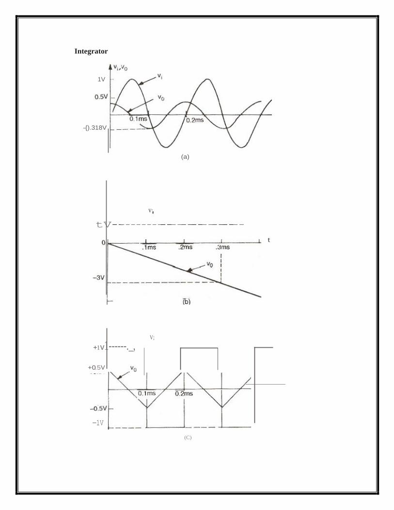
Integrator
1V
-).318V
(a)
v·I
tV--------------------------
t
V;
+1v1------._,
+0.5V
-1V
(C)

b
RESULT:
Differentiator
f 1
2R1Cf
T>Rf C1=
Integrator
1 fa =
2RfCf
T=

4. ACTIVE FILTERAPPLICATIONS-LPF, HPF [ FIRSTORDER ]
AIM: TostudyOp-AmpasfirsorderLPFandfirstorderHPFandtoobtainfrequency
response.
APPARATUS:
1. IC 741.
2. Resistors (10KΩ--2, 560Ω, 330Ω
3. Capacitors(0.1Ω)
4. Bread board trainer
5. CRO
6. Function generator
7. connecting wires
8. Patch cards.
CIRCUIT
DIAGRAM: (a)
LPF

(a)HPF
THEORY:
LOWPASS FILTER:
ThefirstorderlowpassbutterworthfilterusesanRcnetworkforfiltering.The op-
ampisusedinthenoninvertingconfiguration,henceitdoesnotloaddowntheRC network. Resistor R1
and R2 determine the gain ofthefilter.
V0/Vin=Af/(1+jf/fh)
Af=1 +Rf/R1=pass band gain offilter .
F=frequency ofthe input signal.
Fh= 1/2ΠRC =High cutt off frequency of filter . V0/Vin =Gain ofthe filter as afunctionoffrequency
ThegainmagnitudeandphaseangleequationsoftheLPFthecanbeobtained by converting
V0/Vin into its equivalent polar form as follows
|V0/Vin|=Af/(√1+(f/fl)2)
Φ = - tan-1(f/fh)
WhereΦisthephaseangleindegrees.TheoperationoftheLPFcanbeverified from the gain magnitude equation.

1. Atvery low frequencies i.e f<fh,
|V0/Vin|=Af. 2. Atf=fh,|V0/Vin|=Af/√2. 3. Atf>fh,|V0/Vin|<Af.
HIGH PASS FILTER:
High pass filters are often formed simply by interchanging frequency.
DeterminingresistorsandcapacitorsinLPFsthatis,afirstorderHPFisformedfroma
firstorderLPFbyinterchangingcomponents‘R’and‘C’figure.Showsafirstorder
butterworthHpFwithalowercutoff frequencyof‘Fl’.Thisisthefrequencyatwhich magnitude ofthe
gain is 0.707times its pass band value. Obviously all frequencies,with the highest frequency
determinate by the closed loop band width ofop-amp.
For the firstorderHPF ,the output voltage is
V0 =[1+ Rf/R1] j2ΠRCVin/(1- j2ΠfRC)
V0/Vin=Af[j(f/fl)/(1=j(f/fl)]
WhereAf+ Rf/R1a pass band gain ofthe filter.
F=frequency ofinput signal.
Fl=1/2ΠRC = lower cutt off frequency
Hence, the magnitude ofthe voltage gain is
|V0/Vin|=Af(f/fl)/√1+(f/f1)2.
Since,HPFsareformedfromLPFssimplybyinterchangingR’sandC’s.The design and
frequency scaling procedures oftheLPFsare also applicable toHPFs.
PROCEDURE:
1. Connections are made as per the circuit diagram.
2. Apply sine wave ofamplitude 4Vp-ptothe non inverting input terminal.
3. Values the input signal frequency. 4. Note down the corresponding output voltage.
5. Calculate gain in db.
6. Tabulate the values.
7. Plot a graph between frequency and gain.
8. Identify stop band and pass band from the graph.
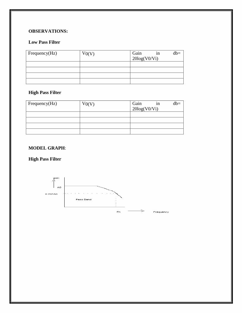
OBSERVATIONS:
Low Pass Filter
Frequency(Hz) V0(V) Gain in db= 20log(V0/Vi)
High Pass Filter
Frequency(Hz) V0(V) Gain in db= 20log(V0/Vi)
MODEL GRAPH:
High Pass Filter

Low Pass Filter
PRECAUTIONS:
1.Make null adjustment before applying the input signal.
2.Maintain proper Vcclevels.
RESULT:
5.ACTIVE FILTER APPLICATIONS
AIM:
To study the op-amp as first order band pass and first order band reject filters and to
obtain the frequency response.
APPARATUS:
1. IC 741.
2. Resistors (10KΩ, 1K Ω, 1.5KΩ)
3. Capacitors (0.01μF)
4. Bread board
5. CRO
6. Function generator
7. Connecting wires
8. Patch cards.
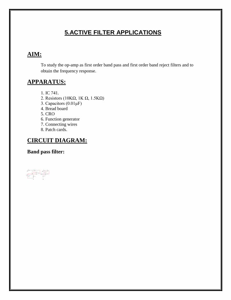
CIRCUIT DIAGRAM:
Band pass filter:
1
2
3
U1
1
2
3
U2
R1
1 k o h m
R2
1 0 k o h m
R4
1 k o h m
R5
1 . 5 k o hm
R3
1 . 5 k o hm
R6
1 0 k o h m
C1
0 . 0 1 u F
C2
0 . 0 1 u F
V1
1 V
0 . 7 1 V_r m s
1 0 0 0 Hz
0 De g

Band reject filter:
R1
1 k o h m
R2
1 k o h m
1
2
3
U1
1
2
3
U2R3
1 k o h m
R4
1 k o h m
R5
1 k o h m
R6
1 k o h m
C2
1 u F
C3
1 u F
V1
1 V
0 . 7 1 V_r m s
1 0 0 0 Hz
0 De g
THEORY:
An electric filter is often a frequency selective circuit that passes a specified band of
frequencies and blocks or attenuates signals of frequencies outside this band.
Analog filters are designed to process analog signals while digital filters process analog
signals using digital techniques depending on the types of elements used in their construction,
filters may be classified as passive or active active. Elements used in passive filters are
resistors, capacitors and inductors, active filters on the other hand employ transistors or op-
amps in addition to the resistors and capacitors.
Each of low pass, high pass, band pass, all pass and band reject filters and used an op-amp as
the active elements and resistors and capacitors as the passive elements. Although the 741
type op-amp works satisfactorily in these filter circuits, high speed op-amps such as the
LM318 or ICL8017 improve slew rates and higher unity gain bandwidths.
PROCEDURE:
1. Connections are made as per the circuit diagram.
2. Apply sine wave of amplitude 4Vp-p to the non inverting input terminal.
3. Values the input signal frequency.
4. Note down the corresponding output voltage.
5. Calculate gain in db.
6. Tabulate the values.
7. Plot a graph between frequency and gain.
8. Identify stop band and pass band from the graph.

OBSERVATIONS:
Band pass filter:
Frequency(Hz) Output voltage(v) Gain(Vo/Vi) Gain in db
Band reject filter:
Frequency(Hz) Output voltage(v) Gain(Vo/Vi) Gain in db
MODEL GRAPH:
Band pass filter:

Band reject filter:
PRECAUTIONS:
1. Make null adjustment before applying the input signal.
2. Maintain proper Vcc levels.
3. Loose connections should be avoided.
RESULT:
The response of band pass filter and band reject filter are verified, plotted and tabulated the
values in tabular column.
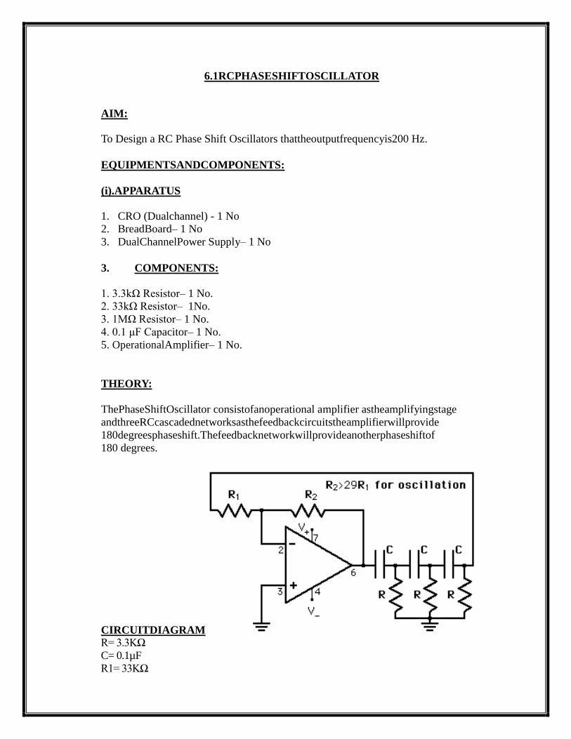
6.1RCPHASESHIFTOSCILLATOR
AIM:
To Design a RC Phase Shift Oscillators thattheoutputfrequencyis200 Hz.
EQUIPMENTSANDCOMPONENTS:
(i).APPARATUS
1. CRO (Dualchannel) - 1 No
2. BreadBoard– 1 No
3. DualChannelPower Supply– 1 No
3. COMPONENTS:
1. 3.3kΩ Resistor– 1 No.
2. 33kΩ Resistor– 1No.
3. 1MΩ Resistor– 1 No.
4. 0.1 μF Capacitor– 1 No.
5. OperationalAmplifier– 1 No.
THEORY:
ThePhaseShiftOscillator consistofanoperational amplifier astheamplifyingstage
andthreeRCcascadednetworksasthefeedbackcircuitstheamplifierwillprovide
180degreesphaseshift.Thefeedbacknetworkwillprovideanotherphaseshiftof
180 degrees.
CIRCUITDIAGRAM R= 3.3KΩ
C= 0.1µF
R1= 33KΩ

PROCEDURE:
i. Constructthecircuitas shown inthecircuitdiagram.
ii.AdjustthepotentiometerRfsuchthatanoutputwaveformisobtained.
iii.Calculatetheoutputwaveformfrequencyandpeaktopeakvoltage.
iv. Comparethetheoreticalandpracticalvaluesof theoutputwaveformfrequency.
OBSERVATIONS:
Thefrequencyof oscillation=
CALCULATIONS:
i.Thefrequencyof oscillationfoisgivenby
fo= 2
1 =
6RC
0.065
RC
ii. The gain Avattheabovefrequencymustbeatleast29
RF
i.e. 29 R1
iii.fo=200Hz
LetC=0.1μFThen
0.065 R=
200X107
3.25k
(choose3.3kΩ)

Topreventtheloadingof theamplifierbecauseof RCnetworksitisnecessarythat
R1≥10RThereforeR1=10R=33kΩ
ThenRF=29 (33 kΩ) =957 kΩ (chooseRF=1MΩ)
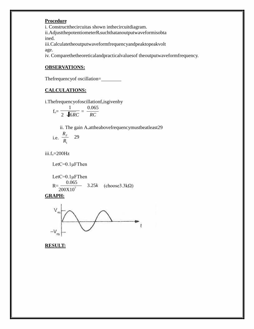
GRAPH:
RESULT:
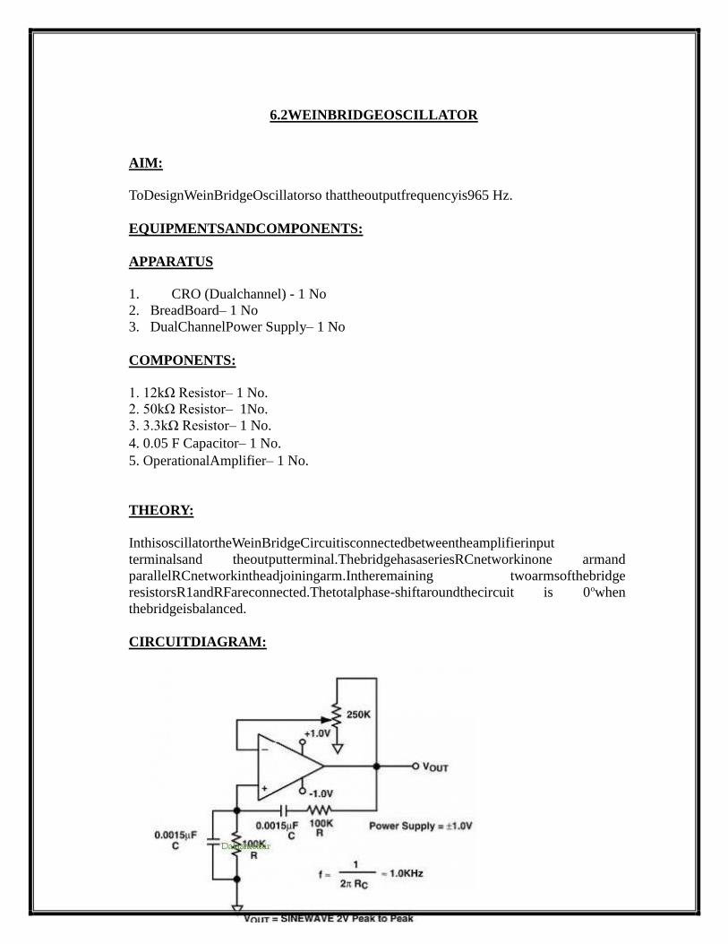
6.2WEINBRIDGEOSCILLATOR
AIM:
ToDesignWeinBridgeOscillatorso thattheoutputfrequencyis965 Hz.
EQUIPMENTSANDCOMPONENTS:
APPARATUS
1. CRO (Dualchannel) - 1 No
2. BreadBoard– 1 No
3. DualChannelPower Supply– 1 No
COMPONENTS:
1. 12kΩ Resistor– 1 No.
2. 50kΩ Resistor– 1No.
3. 3.3kΩ Resistor– 1 No.
4. 0.05 F Capacitor– 1 No.
5. OperationalAmplifier– 1 No.
THEORY:
InthisoscillatortheWeinBridgeCircuitisconnectedbetweentheamplifierinput
terminalsand theoutputterminal.ThebridgehasaseriesRCnetworkinone armand
parallelRCnetworkintheadjoiningarm.Intheremaining twoarmsofthebridge
resistorsR1andRFareconnected.Thetotalphase-shiftaroundthecircuit is 0owhen
thebridgeisbalanced.
CIRCUITDIAGRAM:
P r o c e d u r e i. Constructthecircuitas shown inthecircuitdiagram.
ii.AdjustthepotentiometerRfsuchthatanoutputwaveformisobta
ined.
iii.Calculatetheoutputwaveformfrequencyandpeaktopeakvolt
age.
iv. Comparethetheoreticalandpracticalvaluesof theoutputwaveformfrequency.
OBSERVATIONS:
Thefrequencyof oscillation=
CALCULATIONS:
i.Thefrequencyofoscillationfoisgivenby
fo= 2
1 =
6RC
0.065
RC
ii. The gain Avattheabovefrequencymustbeatleast29
RF
i.e. 29 R1
iii.fo=200Hz
LetC=0.1μFThen
LetC=0.1μFThen
0.065 R=
200X107
3.25k
(choose3.3kΩ)
GRAPH:
RESULT:

7.FUNCTION GENERATOR USING OP AMPS
AIM: Togeneratetriangularandsquarewaveformsandtodeterminethetimeperiod
ofthe waveforms.
APPARATUS:
1. Op-Amp IC 741 –2 Nos
2.Bread board IC trainer
3.Capacitor 0.1µF
4.Zener diodes (6.2V)—2 Nos
5.Resistors—10KΩ, 150KΩ1.5KΩ, 1MΩ, 8.2KΩCRO
6.Patch cards
7.Connecting wires
CIRCUIT DIAGRAM:

THEORY:
Thefunctiongeneratorconsistsof acomparatorU1andanintegratorA2.The comparator U2
compares the voltage atpointPcontinuously with the inverting input i.e.,
atzerovolts.WhenvoltageatPgoesslightlybeloworabovezerovolts,theoutputof U1 is atthe negative
or positive saturation level, respectively.
ToillustratethecircuitoperationletussettheoutputofU1atpositivesaturation
+Vsat(approximately+Vcc). This+VsatisaninputtotheintegratorU2.Theoutputof
U2,thereforewillbea negative goingramp.Thus,one end ofthevoltagedivider R2-R3
isthepositivesaturationvoltage+VastofU1andtheotheristhenegativegoingramp ofU2.
Whenthenegativegoingrampattainsacertainvalue–Vramp,pointpisslightlybelowzerovalts;
hencetheoutputofU1willswitchfrompositivesaturationtonegative saturation–Vsat(approximately–
Vcc). ThismeansthattheoutputofU2willnowstop goingnegativelyandwillbegintogopositively.The
outputofU2willcontinue to
increaseuntilitreaches+Vramp.AtthistimethepointPisslightlyabovezerovolts.
Thesequencethenrepeats.Thefrequenciesofthesquareareafunctionofthed.csupplyvoltage.Desireda
mplitudecanbeobtained by usingapproximatezenersatthe output ofU1.
THEORETICAL VALUES:
Time period, T=4R5C (R3+R4)/(R1+R2) =0.492 msec.
Positive peak ramp =VzR5/(R1+R2) =0.05 volts.
PRACTICAL VALUES:
Timeperiodsoftriangular wave=
Time periods ofsquare wave=
Positive peak ramp=
Voltage ofsquare wave= PROCEDURE:
1. The circuit is connected as shown in the figure.
2. TheoutputofthecomparatorU1isconnectedtotheCROthroughchennal1,to generate a square
wave.
3. TheoutputofthecomparatorU2isconnectedtotheCROthroughchennal2,to generate a
triangular wave.
4. Thetimeperiodsofthesquarewaveandtriangularwavesarenotedandtheyare found tobe equal.

MODEL GRAPH:
PRECAUTIONS:
1.Make null adjustment before applying the input signal.
2.Maintain proper Vcclevels.
RESULT:
8. IC 555 TIMER-MONOSTABLECIRCUIT
AIM:
timer.
Toconstructandstudytheoperationofamonostablemultivibratorusing555IC
APPARATUS:
1. 555 IC timer
2. Capacitors (0.1µF,0.01µF)
3. Resistors 10KΩ
4. Bread board IC trainer
5. CRO
6. Connecting wires and Patchcards
THEORY:
Monostablemultivibratorisalsoknownastriangularwavegenerator.Ithasonestableandonequa
sistablestate.Thecircuitisusefulforgenerating single outputpulseoftimedurationin response
toatriggeringsignal. The width of the output pulse
dependsonlyonexternalcomponentsconnectedtotheop-amp.Thediodegives a
negativetriggeringpulse.Whentheoutputis+Vsat, adiodeclampsthecapacitor voltage to0.7V. then,
anegativegoingtriggeringimpulsemagnitudeVipassing through RC and the negative triggering
pulse is applied tothe positive terminal.
Letusassumethatthecircuitisinstablestate.TheoutputV0iisat+Vsat.The
diodeD1conductsandVcthevoltageacrossthecapacitor‘C’getsclampedto0.7V.thevoltageatthepositi
veinputterminalthroughR1R2potentiometerdivideris+ßVsat.
Now,ifanegativetriggerofmagnitudeViisappliedtothepositiveterminalsothat the
effectivesignalislessthan0.7V.theoutputoftheOp-Ampwillswitchfrom+Vsat to– Vsat.
Thediodewillnowgetreversebiasedandthecapacitorstartschargingexponentiallyto–
Vsat.WhenthecapacitorchargeVcbecomesslightlymorenegative than–ßVsat, theoutputoftheop-
ampswitchesbackto+Vsat.Thecapacitor‘C’nowstartschargingto+Vsatthrough R until Vcis 0.7V.
t/RC V0=Vf +(Vi-Vf) е .
ß=R2/(R1+R2)
IfVsat>>Vpand R1=R2and ß=0.5, Then, T=0.69RC.

CIRCUIT DIAGRAM:
PROCEDURE:
1. Connections are made as per the circuit diagram.
2. Negative triggering is applied atthe terminal 2.
3. The output voltage is measured by connecting the channel-1 at pin3.
4. Theoutputvoltageacrosscapacitorismeasuredbyconnectingthechannel-2at the point ‘P’.
5. TheoreticallythetimeperiodiscalculatedbyT=1.1R1C1 whereR1 =10KΩ
C1=0.1µF. 6. Practically thecharginganddischargingtimersaremeasuredandtheoretical
valueoftime period is measured with practical value

MODELGRAPH:
PRECAUTIONS:
1.Make the null adjustment before applying the inputsignal.
2.Maintain proper vcc levels.
RESULT:

9. IC 555 TIMER-ASTABLECIRCUIT
AIM: Toconstruct and study the operation ofAstablemultivibrator using 555 timer
APPARATUS:
1.IC 555 Timer
2.Resistors (10 KΩ,4.7 KΩ)
3.Diode (IN 4007)
4.Capacitors (0.1µF,0.01µF)
5.CRO
6.Patch cards
7.CRO Probes
8.Connecting wires
CIRCUIT DIAGRAM:

THEORY:
A simple OPAMP astable multivibrator is also called square wave generator and free
running oscillator .The principle for the generation of square wave output is to force an OP_AMP
to operate in the saturation region β=R2/(R1+R2) of the output is feedback to input. The output
isalsofeedbacktothenegativeinputterminalafterintegratingbymeansofaRCLPFwheneverthenegative
inputjustexceedsVref,switching takes placeresultinginasquarewaveoutput.Inastablemultivibrator
both states are quasi stable states.
When the output is +Vsat, the capacitor is now starts charging towards +Vsat through
resistance R the voltage is held at +βVsat. This condition continuous until the charge on C just
exceedβVsat.Then the capacitor begins to dischargetowards–
Vsat.Thenthecapacitorchargesmoreand more negatively untilitsvoltagejust–
βVsat.Thefrequencyisdeterminedbythetimeittakesthecapacitortocharge from– βVsat and +βVsat
Vc(t)=Vf+(Vi-Vf)e-t/RC
Vc(t)=Vsat-Vsat(1+β)e-t/RC
We getT1=RC ln((1+β)/(1-β))
T=2T1=2 RC ln ((1+β)/(1-β)),Vo(p-p)=2Vsat
PROCEDURE: 1.Connections are made as per the circuit diagram.
2.Pins 4 and 8 are shorted and connected topower supply Vcc(+5V)
3.Between pins 8 and 7 resistor R1 of10KΩ is connected and between
7 and 6 resistor R2 of4.7KΩ is connected. Pins 2 and 6 short circuited.
4.Inbetween pins 1 and 5 a Capacitor of0.01µF is connected.
5.Theout put is connected across the pin 3 and GND.
6. In between pins 6 and GND a Capacitor of 0.1μF is connected.
7.Theoreticallywith out diode charging time Tcis given by
Tc=0.69(R1+R2) C1,
Discharging time Tdis given by Td=0.69R2C1
The frequency fis given by f=1.45/(R1+2R2)C1
%of Duty cycle is (Tc/(Tc+Td))*100
8.PracticallyTdandTcare measured and wave forms are noted and theoretical
Values are verified with practical values
9.Connect diode between pins 7 and 2.
10. Theoretically with diode connected charging time is given by Tc=0.69R1C1
Discharging time is given by Td=0.69R2C1
11. Practically TdandTcare noted and verified with theoretical values

OBSERVATIONS:
With diode without diode
Theoretical Practical Theoretical Practical
MODEL GRAPH:
PRECAUTIONS:
1.Make null adjustment before applying the input signal.
2.Maintain proper Vcclevels.
RESULT:

10. SCHMIT TRIGGER USING IC 741
Aim:
To construct the Schmitt trigger using Ic 741
Apparatus:
1. 741 IC 2. Function Generator
3. Bread board
4. Resistors
5. Power supply 6. Connection wire
Circuit Diagram

11.IC 565PLL
AIM:
1. Tostudytheoperationof NE565 PLL
2. Touse NE565 as amultiplier
EQUIPMENTSANDCOMPONENTS:
APPARATUS
1. DC power supply
2. CRO
- 1 No.
-
1 No.
3. BreadBoard - 1 No.
4. FunctionGenerator- 1 No.
COMPONENTS:
1. 6.8 kΩ Resistor– 1 No.
2. 0.1 F Capacitor– 1 No
5. 0.001 F Capacitor– 2 Nos
6. IC565 - 1 No.
THEORY: The565isavailableasa14-pinDIPpackage.Itisproducedbysignaticcorporation.
Theoutputfrequencyof theVCO canbe rewrittenas
0.25 fo Hz
RTCT
Where RT and CTare the external resistor and capacitor connected to pin8 and pin9. A
value between 2k and 20k is recommended for RT .The VCO free running frequency
is adjusted with RTand CT to be at the centre for the input frequency range.

CIRCUITDIAGRAM:
PROCEDURE:
i. Connectthecircuitusingthecomponentvaluesas shown inthefigure
ii .MeasurethefreerunningfrequencyofVCO at pin4 withtheinputsignalVinset=
zero.Compareitwiththecalculatedvalue=0.25/RTCT
iii. Now apply the input signal of 1Vpp squarewaveata1kHz topin2
iv. Connect1 channelof thescopetopin2 anddisplaythissignalon thescope

v .GraduallyincreasetheinputfrequencytillthePLLislockedtotheinputfrequency. This
frequency f1 gives the lower ends of the capture range. Go on increase the input
frequency, till PLL tracks the input signal, say to a frequency f2.This frequency f2
gives the upper end of the lock range. If the input frequency is increased further the
loop will get unlocked.
vi. Now graduallydecreasetheinputfrequencytillthePLLisagainlocked.Thisis the
frequency f3, the upper end of the capture range .Keep on decreasing the input
frequency until the loop is unlocked. This frequency f4 gives the lower end of the lock
range
vii. The lock range fL=(f2– f4) compareitwiththecalculatedvalueof 7.8fo
12
Also thecapturerangeis fc=(f3– f1). Compareitwiththecalculatedvalueof
capturerange.
f fL
c (2 )(3.6)(10
3)xC)
1/2
viii. To use PLL as a multiplie5r,makeconnectionsas show in fig. The circuit uses a
4-bitbinarycounter7490 usedasadivide-by-5circuit.
ix.Settheinputsignalat1Vpp squarewaveat500Hz
x..Vary the VCO frequencybyadjustingthe20KpotentiometertillthePLLis locked.
Measure the output frequency
xi. Repeatstep9 and10 for input frequency of 1kHzand1.5kHz.
OBSERVATIONS:
fo =
fL=
fC=
CALCULATIONS:
fL=(f2– f4) = 7.8fo
12
fc=(f3– f1) =
fL
(2 )(3.6)(103)xC)
1/2

GRAPH:
RESULT:
fo=
fL=
fC=

12.IC 566 –VCO APPLICATIONS
AIM: Tooperatethe NE/SE566 asVoltageControlledOscillatorandtofind the
frequenciesforvarious values ofR1and C1;
APPARATUS: 1.IC NE/SE566
2.Resistors (1KΩ,5KΩ,4KΩ,6KΩ,8KΩ)
3.Capacitors(0.001μF,0.0001μF)
3.Function generator
4.Regulated power supply
5.IC bread board trainer
6.CRO
7.Patch cards and CRO probes
CIRCUIT DIAGRAM:

THEORY:
VoltageControlledOscillatorisalsocalledasvoltagetofrequencyconverter.Itprovidesthesimul
taneoussquarewaveandtriangularwaveoutput.Thefrequencyofoutputwaveisthefunctionofinputvolta
ge,hencethenameVoltageControlledOscillator.Outputfrequencyisalsothefunctionofexternalresistor
R1andcapacitorC1.
PROCEDURE:
1.Connections are made as per the circuit diagram.
2.Measure the output voltage and frequency ofboth triangular and squares.
3.Vary the values ofR1and C1and measure the frequency ofthe waveforms.
4.Compare the measured values with the theoretical values.
OBSERVATIONS:
Sl.
No.
R1
C1
OutputVoltage (V)
Theoretical frequency (KHz)
2(VVC) fO =
R1C1V
Practical
frequenc
y (KHz) Square wave
Triangular wave

MODEL GRAPH:
PRECAUTIONS:
1.Connect the wires properly.
2.Maintain proper Vcclevels.
RESULT:

13.VOLTAGE REGULATORUSING IC 723
AIM: Toplot the regulation characteristics ofthegiven IC LM 723.
APPARATUS:
1. Bread board
2. IC LM 723
3. Resistors(7.8KΩ ,3.9KΩ )
4. RPS
5. DRB
6. Capacitors 100µF
7. Patch cards
8. Connecting wires
CIRCUIT DIAGRAM:
THEORY: Avoltageregulatorisacircuitthatsuppliesconstantvoltageregardlessof changes inload
currents. Except for the switching regulators, all other types of
regulatorsarecalledlinearregulators.ICLM723isgeneralpurposeregulator.The
inputvoltageofthis723ICis40Vmaximum.Outputvoltageadjustablefrom2Vto30
V. 150mAoutput current external pass transistor. Out putcurrents in excess of
10Amperepossiblebyaddingexternaltransistors.Itcan beusedaseitheralinearora
switchingregulator.ThevariationofDCoutputvoltageasafunctionofDCloadcurrent is called
regulation.
% Regulation =[(Vnl-Vfl)/Vfl]*100
PROCEDURE:
(1).LINE
REGULATION
1.Connections are made as per the circuit diagram
2.Power supply is connected to12 and 7 terminals
3.Volt meter is connected to10 and 7 terminals
4.Byincreasing the input voltage corresponding volt meter reading is noted.
(2).LOAD REGULATION value
1.Connect the load tothe terminals 10 and GND.
2.Keep the input voltage constant atwhich line regulation is obtained
3.The maximum load value is calculated from IC ratings.
4.Now,wedecreasetheloadresistanceandnotedownthecorresponding
Ofthe output in volt meter.
5.Plot the graph forload verses load regulation.
OBSERVATIONS:
(1).LINEREGULATION:
Vnl=
Line voltage (V) Outputvoltage(V)

(2).LOAD REGULATION:
Regulated
output(V)
Load
current(mA)
Load
resistance(KΩ)
Load
regulation
% REGULATION=[(Vnl-Vfl)/Vfl]*100 MODEL GRAPH:
PRECAUTIONS:
1.Whiletakingthereadingsofregulatedoutputvoltageloadregulation ,keep the input voltage
constant at15V.
2.Donotincrease the input voltage morethan 30 Vwhile taking thereadingforno load
condition?
RESULT:

14.Three Terminal Voltage Regulators (7805, 7809 And 7912)
AIM:
To verify the operation of three terminal fixed voltage regulators 7805, 7809, 7912 and also to
find out their line and load regulation.
APPARATUS:
S.No. Name of the
component
Range Quantity
1. 7805 -- 1
2. 7809 -- 1
3. 7912 -- 1
4. Capacitors 0.33µf
0.1µf
1
1
5. Multimeter (0-
30)v
1
6. Power
Supply
1
CIRCUIT DIAGRAM:

THEORY:
Three terminal voltage regulators have three terminals which are unregulated
input (Vin), regulated output (Vo) and common or a ground terminal. These
regulators do not require any feedback connections.
Positive voltage regulators:
78xx is the series of three terminal positive voltage regulators in which xx indicate
the output voltage rating of the IC.
7805:
This is a three terminal regulator which gives a regulated output of +5V fixed. The
maximum unregulated input voltage which can be applied to 7805 is 35V.
7809:
This is also three terminal fixed regulator which gives regulated voltage of +9V.
Negative voltage regulators:
79xx is the series of negative voltage regulators which gives a fixed negative
voltage as output according to the value of xx.
7912:
This is a negative three terminal voltage regulator which gives a output of -12V.
Line Regulation:
It is defined as the change in the output voltage for a given change in the input
voltage. It is expressed as a percentage of output voltage or in millivolts.
%RL = ΔVo/ΔVin x 100
Load Regulation:
It is the change in output voltage over a given range of load currents that is from
full load to no load. It is usually expressed in millivolts or as a percentage of
output voltage.
%R Load = [(Vnl-Vfl)/Vnl] x100
PROCEDURE:
1. Connect the circuit as shown in the figure.
2. Apply unregulated voltage from 7.5V to 35V and observe the output
voltage.
3. Calculate the line and load regulation for the regulator.
4. Plot the graphs from the observations.
5. Repeat the same for the remaining regulators.
Result

15. 4 BIT DAC USING OP AMP
AIM: Toconstruct and study digital toanalog converter circuit.
APPARATUS:
IC 741
Multi meters Patch
cards Connecting
wires Resistors 1k,
2k,8k
IC bread board trainer
CIRCUIT DIAGRAM:
(a) Weighted resistor DAC:
(b)R-2R ladder DAC

THEORY:
Adigitaltoanalogconverterisusedwhenabinaryoutputfromadigitalsystemmustbeconvertedt
oequivalentanalogvoltageorcurrent.ADACconverterusesan op amp and binary weighted resistors
or R-2r ladder resistors.
Weighted resistor DAC:
Ithas n electronic switches –d1, d2, d3……….dncontrolled by binary input
Word.Theseswitches are single pole double throw type.Ifthebinary input toaparticularswitch
is1,itconnectsresistance tothereference voltage(-vr).Andiftheinput is0,theswitch
connectstheresistortotheground.TheoutputcurrentI0for anidealop amp can be written
asI0=I1+I2+…………..In
Vr/2Rd1+Vr/4Rd2+…….+Vr/2nRdn=V0=I0Rf=VrRf/R(d1,2….n)
TheweightedresistorDACcircuitusesanegativereferencevoltage.Theanalogoutputvoltageisp
ositivestaircase.Fora3bitweightedresistorDAC(1)iftheopamp
isconnectedinnoninvertingmode,itcanbeconnectedinnoninvertingmodealso
.(2)Theopampisworkingascurrenttovoltage converter.(3)Thepolarityofreference voltage is in
accordance with type ofswitch used.
R-2R ladder DAC:
Inbinaryweightedresistorsmethodareused.ThiscanbeavoidedbyusingR-
2R ladder typeDACwhereonly 2values ofresistorsarerequired .Thebinaryinputsare
simulatedbyswitchesB0-B3andoutputisproportionaltothebinaryinputs.Binary inputs can be high
(+5V)or low(0V). PROCEDURE:
1.Connections are made as per circuit diagram.
2.Pin2 is connected toresistor 1MΩand ground.
3.+Vccare available atPin7 and –Vcc is applied atPin4.
4.Outputis taken between pin6 and ground
5.Voltageateach bit (vr) is found atbits b0, b1, b2, b3.
6.Pin3ofop amp is connected toresistor 1kΩ and is given to b3 (msb).
7.Aresistor of2kΩ is connected between pin2 and pin 6 of op amp.

OBSERVATIONS:
D3 D2 D1 D0 Binary weighted
resistor(v)
Theoretical practical
R-2R ladder DAC (v)
Theoretical practical
RESULT: