description 2 rev 4.2 block diagram m i c b i a s d g n d d a c a d c r e f, d a c r e f avdd agnd 5...
TRANSCRIPT

Ultra-Low Power Stereo CODEC with Audio Enhancement DSP, 2W Stereo Class D Speaker Drivers and Ground
Referenced Headphone Drivers
http://www.cirrus.com
Copyright Cirrus Logic, Inc., 2013–2016
(All Rights Reserved)
Rev 4.2
AUG ‘16
WM8963
DESCRIPTION
The WM8963 is a low power, high performance stereo CODEC
designed for portable digital audio applications.
An integrated charge pump provides a ground referenced output
which removes the need for DC-blocking capacitors on the
headphone outputs, and uses the Wolfson ‘Class-W’ amplifier
techniques—incorporating an innovative dual-mode charge
pump architecture—to optimise efficiency and power
consumption during playback. A DC Servo is used to reduce DC
ground offsets. This improves power consumption and
minimises pops and clicks.
Stereo class D speaker drivers provide 2W per channel into 4
loads with a 5V supply. Low leakage, excellent PSRR and
pop/click suppression mechanisms also allow direct battery
connection to the speaker supply. Flexible speaker boost
settings allow speaker output power to be maximised while
minimising other analogue supply currents.
Control sequences for audio path setup can be pre-loaded and
executed by an integrated sequencer to reduce software driver
development and eliminate pops and clicks via Cirrus Logic’s
SilentSwitch™ technology.
Flexible input configuration: four stereo or eight mono analogue
inputs on Left or Right ADC. A two-channel digital microphone
interface is also supported. External component requirements
are drastically reduced as no separate microphone, speaker or
headphone amplifiers are required. Advanced on-chip digital
signal processing performs automatic level control for the
microphone or line input.
Stereo 24-bit sigma-delta ADCs and DACs are used with low
power over-sampling digital interpolation and decimation filters
and a flexible digital audio interface.
A programmable audio enhancement DSP is included with
multiple preset algorithms. Virtual Surround Sound (VSS)
widens the stereo speaker audio image, and ReTuneTM can be
used to flatten the frequency response of an external speaker.
The Multi-band Compressor (MBC) can maximize the loudness
of an audio signal, without overdriving the speaker. The
configurable DSP also includes 3D widening for recording, a 5-
band parametric EQ, and Dynamic Range Controller.
A high performance Frequency Locked Loop (FLL) is provided,
to enable flexible system clocking. An internal oscillator (using
external crystal) is also provided. Clock output signals, derived
from the FLL, can also be enabled to support synchronous
clocking of external circuits.
The WM8963 supports 1.8V external supplies. 1.2V digital core
supply is supported, for low power operation. Speaker supplies
up to 5.5V (including direct connection to a battery) enable
maximum speaker output power. Unused functions can be
disabled using software control to save power.
The WM8963 is supplied in a very small W-CSP package, ideal
for use in hand-held and portable systems.
FEATURES
DAC SNR 98dB (‘A’ weighted), THD -84dB at 48kHz, 1.8V
ADC SNR 94dB (‘A’ weighted), THD -85dB at 48kHz, 1.8V
Stereo Class D Speaker Driver
- 2W per channel into 4 BTL speakers
- 2W mono mode (for improved THD)
- Flexible internal switching clock
Wolfson ‘Class-W’ ultra-low power headphone driver
- Up to 31mW per channel output power at 1% THD+N
- Support for 2 stereo headphone outputs
- Ground Referenced
- Low offset (+/- 1.4mV)
- Pop and click suppression
Microphone Interface
- Four stereo, single-ended analogue inputs
- Digital microphone interface
- Integrated low noise MICBIAS
- Integrated LDO to generate MICVDD supply
- Programmable ALC / Limiter and Noise Gate
Programmable Audio Enhancement DSP with Presets
- Virtual Surround Sound
- ReTuneTM frequency linearisation
- Multi-Band Compression (MBC)
Fixed Audio Processing DSP
- LPF/HPF
- 3D stereo widening
- 5-band Parametric EQ
- Dynamic range controller
- Beep generator
Integrated FLL for flexible audio system clocking
- External clock outputs from FLL
Low power consumption
- 5.0mW headphone playback
- 6.1mW analogue record mode
- 1.8V analogue & digital I/O supplies
- 1.2V digital core supply, for low power operation.
1.7V (min) required for full range of clocking ratios
- 5.5V (max) speaker supply for high power output
2-wire I2C and 3- or 4-wire SPI serial control interface
Standard sample rates from 8kHz to 96kHz
W-CSP, 3.6mm x 3.9mm, 49-pin
APPLICATIONS
Portable gaming
Voice recorders
Mobile multimedia
Stereo DSC-Camcorder

WM8963
2 Rev 4.2
BLOCK DIAGRAM
MIC
BIA
S
DG
ND
DA
C
AD
CR
EF
,
DA
CR
EF
AVDD
AGND
VMIDC50
k5
0k
DA
C
ADCDAT
DACDAT
BCLK
LRCLK
MICVDD
DA
C S
ign
al
En
ha
nce
me
nt
5-B
an
d E
Q
DR
C
2n
d o
rde
r H
PF
VS
S
ReT
un
eT
M
MB
C
DC
VD
D
DA
C
Dig
ita
l F
ilte
rs
Dig
ita
l V
olu
me
AD
C S
ign
al
En
ha
nce
me
nt
2n
d o
rde
r H
PF
1st o
rde
r L
PF
/HP
F
3D
Su
rro
un
d
DF
1 F
ilte
r
DR
C DIG
ITA
L A
UD
IO
INT
ER
FA
CE
A-la
w a
nd
u-la
w s
up
po
rt
WW
M8
96
3
T-L
oo
pb
ack
mix
er
DB
VD
D
CH
AR
GE
PU
MP CPCB
CPVDD
CPGND
CPCA
CP
VO
UT
PC
PV
OU
TN
SP
KG
ND
1S
PK
VD
D1
SP
KG
ND
2S
PK
VD
D2
LD
OM
ICV
DD
LD
OV
DD
MCLK/XTI
CLKOUT5
XTO
CLKOUT2/GPIO2
Oscill
ato
r &
FL
LC
ON
TR
OL
INT
ER
FA
CE
SDA
SCLK
CIFMODE
Dig
ita
l M
ic
Inte
rfa
ce
GP
IOs
GPIO5
CS/GPIO6
HP
OU
T1
L
HP
OU
T1
R
SP
KO
UT
LP
SP
KO
UT
LN
SP
KO
UT
RP
SP
KO
UT
RN
CL
AS
S D
CL
AS
S D
Ca
ple
ss
HP
HP
OU
TF
B
HP
OU
T2
L
HP
OU
T2
R
0d
B to
+9
dB
1.5
dB
ste
ps,
an
d +
12
dB
0d
B to
+9
dB
1.5
dB
ste
ps,
an
d +
12d
B
-7 to
0d
B
1d
B s
tep
s
-7 to
0d
B
1d
B s
tep
s
-68d
B t
o 6
dB
1d
B s
tep
s,
mu
te
Ca
ple
ss
HP
-68d
B to
6d
B
1d
B s
tep
s,
mu
te
++
-68d
B to
6d
B
1d
B s
tep
s,
mu
te
-68
dB
to
6d
B
1d
B s
tep
s,
mu
te
Dig
ita
l B
ee
p
Ge
ne
rato
r
IN4
L
-23.2
5 t
o +
24dB
,0.7
5dB
ste
psIN
1L
A
DC
IN3
L
IN2
L
A
DC
IN4
R
IN1
R
IN3
R
IN2
R
VM
ID
VM
ID
AD
C
Dig
ita
l F
ilte
rs
AL
C
Mo
no
Mix
Dig
ita
l V
olu
me
++
+ +-23.2
5 t
o +
24dB
,0.7
5dB
ste
ps

WM8963
Rev 4.2 3
TABLE OF CONTENTS
DESCRIPTION ................................................................................................................ 1
FEATURES ..................................................................................................................... 1
APPLICATIONS ............................................................................................................. 1
BLOCK DIAGRAM ......................................................................................................... 2
TABLE OF CONTENTS .................................................................................................. 3
PIN CONFIGURATION ................................................................................................... 7
ORDERING INFORMATION ........................................................................................... 7
PIN DESCRIPTION ......................................................................................................... 8
ABSOLUTE MAXIMUM RATINGS ................................................................................. 9
RECOMMENDED OPERATING CONDITIONS ............................................................ 10
ELECTRICAL CHARACTERISTICS ............................................................................ 11 TERMINOLOGY ....................................................................................................................... 20
TYPICAL POWER CONSUMPTION ............................................................................. 21
SIGNAL TIMING REQUIREMENTS ............................................................................. 23 MASTER CLOCK ..................................................................................................................... 23 AUDIO INTERFACE TIMING ................................................................................................... 24
DIGITAL MICROPHONE (DMIC) INTERFACE TIMING ........................................................................................ 24 DIGITAL AUDIO INTERFACE - MASTER MODE ................................................................................................. 25 DIGITAL AUDIO INTERFACE - SLAVE MODE ..................................................................................................... 26 DIGITAL AUDIO INTERFACE - TDM MODE ......................................................................................................... 27
CONTROL INTERFACE TIMING ............................................................................................. 28 2-WIRE (I2C) CONTROL MODE ........................................................................................................................... 28 3-WIRE (SPI) CONTROL MODE ........................................................................................................................... 29 4-WIRE (SPI) CONTROL MODE ........................................................................................................................... 30
POWER ON RESET TIMING ................................................................................................... 31 DEVICE DESCRIPTION ............................................................................................... 33
INTRODUCTION ...................................................................................................................... 33 INPUT SIGNAL PATH .............................................................................................................. 34
MICROPHONE INPUT CONNECTION ................................................................................................................. 35 LINE INPUT CONNECTION .................................................................................................................................. 35 MICROPHONE BIAS CONTROL .......................................................................................................................... 36 MICBIAS CURRENT DETECT .............................................................................................................................. 37 MICBIAS CURRENT DETECT FILTERING ........................................................................................................... 39 MICROPHONE HOOK SWITCH DETECTION ...................................................................................................... 40 INPUT PGA ENABLE ............................................................................................................................................ 41 INPUT PGA CONFIGURATION ............................................................................................................................ 42 INPUT PGA VOLUME CONTROL ......................................................................................................................... 42 INPUT MIXER ENABLE ......................................................................................................................................... 45 INPUT MIXER CONFIGURATION AND VOLUME CONTROL .............................................................................. 45
AUTOMATIC LEVEL CONTROL (ALC) ................................................................................... 47 LIMITER MODE ..................................................................................................................................................... 49 ALC GAIN CONTROL ............................................................................................................................................ 51 ALC DYNAMIC CHARACTERISTICS.................................................................................................................... 52 PEAK LIMITER ...................................................................................................................................................... 54 ALC NOISE GATE ................................................................................................................................................. 55 ALC STATUS READBACK .................................................................................................................................... 59
DIGITAL MICROPHONE INTERFACE .................................................................................... 60 ANALOGUE TO DIGITAL CONVERTER (ADC) ...................................................................... 63
ADC CLOCKING CONTROL ................................................................................................................................. 63 ADC DIGITAL VOLUME CONTROL ...................................................................................................................... 64 ADC OVERSAMPLING RATIO (OSR) ................................................................................................................... 66

WM8963
4 Rev 4.2
ADC MONOMIX ..................................................................................................................................................... 66 DSP SIGNAL ENHANCEMENTS ............................................................................................. 67
ENABLE SEQUENCE - ENHANCEMENTS INITIALLY DISABLED ...................................................................... 67 ENABLE / DISABLE SEQUENCE - ENHANCEMENTS INITIALLY ENABLED ..................................................... 68 DISABLE ALL SOUND ENHANCEMENTS SEQUENCE ...................................................................................... 69 UPDATE / READBACK SEQUENCE - ENHANCEMENTS INITIALLY ENABLED ................................................ 70 UPDATE / READBACK SEQUENCE - ENHANCEMENTS INITIALLY DISABLED ............................................... 71
ADC SIGNAL PATH ENHANCEMENTS .................................................................................. 72 ADC SECOND ORDER HIGH-PASS FILTER ....................................................................................................... 72 LOW-PASS / HIGH-PASS FILTER (LPF/HPF) ...................................................................................................... 74 3D SURROUND .................................................................................................................................................... 75 DF1 FILTER ........................................................................................................................................................... 78 DYNAMIC RANGE CONTROL (DRC) ................................................................................................................... 80
DIGITAL MIXING ...................................................................................................................... 87 DIGITAL MIXING PATHS ...................................................................................................................................... 87 DIGITAL SIDETONE.............................................................................................................................................. 88 T-LOOPBACK ........................................................................................................................................................ 90
DAC SIGNAL PATH ENHANCEMENTS .................................................................................. 92 5-BAND EQ ........................................................................................................................................................... 92 DYNAMIC RANGE CONTROL (DRC) ................................................................................................................... 96 DAC SECOND ORDER HIGH-PASS FILTER ....................................................................................................... 97 VIRTUAL SURROUND SOUND (VSS) .................................................................................................................. 98 DAC RETUNE ....................................................................................................................................................... 99 MULTIBAND COMPRESSOR (MBC) .................................................................................................................. 100
DIGITAL-TO-ANALOGUE CONVERTER (DAC) ................................................................... 101 DAC CLOCKING CONTROL ............................................................................................................................... 101 DAC DIGITAL VOLUME CONTROL .................................................................................................................... 102 DAC SOFT MUTE AND UN-MUTE ..................................................................................................................... 104 DAC AUTO-MUTE ............................................................................................................................................... 106 DAC MONO MIX .................................................................................................................................................. 106 DAC DE-EMPHASIS............................................................................................................................................ 107 DAC OVERSAMPLING RATIO (OSR) ................................................................................................................. 107
DIGITAL BEEP GENERATOR ............................................................................................... 108 OUTPUT SIGNAL PATH ........................................................................................................ 109
OUTPUT SIGNAL PATHS ENABLE .................................................................................................................... 110 HEADPHONE SIGNAL PATHS ENABLE ............................................................................................................ 111 SPEAKER MIXER CONTROL ............................................................................................................................. 114 HEADPHONE OUTPUT PGA CONTROL ........................................................................................................... 118 SPEAKER OUTPUT PGA CONTROL ................................................................................................................. 121
ANALOGUE OUTPUTS ......................................................................................................... 124 SPEAKER OUTPUT CONFIGURATIONS ........................................................................................................... 124 HEADPHONE OUTPUT CONFIGURATIONS ..................................................................................................... 126
CHARGE PUMP ..................................................................................................................... 127 DC SERVO ............................................................................................................................. 129
DC SERVO ENABLE AND START-UP ................................................................................................................ 129 DC SERVO ACTIVE MODES .............................................................................................................................. 131
REFERENCE VOLTAGES AND BIAS CONTROL ................................................................ 132 ANALOGUE REFERENCE AND MASTER BIAS ................................................................................................ 132 INPUT SIGNAL PATH BIAS CONTROL SETTINGS ........................................................................................... 133 OUTPUT SIGNAL PATH BIAS CONTROL SETTINGS ....................................................................................... 134
DIGITAL AUDIO INTERFACE ................................................................................................ 135 MASTER AND SLAVE MODE OPERATION ....................................................................................................... 135 OPERATION WITH TDM ..................................................................................................................................... 136 BCLK FREQUENCY ............................................................................................................................................ 137 AUDIO DATA FORMATS (NORMAL MODE) ...................................................................................................... 137

WM8963
Rev 4.2 5
AUDIO DATA FORMATS (TDM MODE) .............................................................................................................. 139 DIGITAL AUDIO INTERFACE CONTROL ............................................................................. 141
AUDIO INTERFACE TRI-STATE ......................................................................................................................... 142 BCLK AND LRCLK CONTROL ............................................................................................................................ 142 COMPANDING .................................................................................................................................................... 143 LOOPBACK ......................................................................................................................................................... 145
CLOCKING AND SAMPLE RATES ....................................................................................... 146 SYSCLK CONTROL ............................................................................................................................................ 148 AUTOMATIC CLOCKING CONFIGURATION ..................................................................................................... 150 DSP, ADC, DAC CLOCK CONTROL ................................................................................................................... 152 CLASS D, 256K, DC SERVO CLOCK CONTROL ............................................................................................... 153 OPCLK CONTROL .............................................................................................................................................. 153 TOCLK, DBCLK CONTROL ................................................................................................................................ 154 BCLK AND LRCLK CONTROL ............................................................................................................................ 155 CONTROL INTERFACE CLOCKING .................................................................................................................. 155
INTERNAL / EXTERNAL CLOCK GENERATION.................................................................. 156 START-UP OPTIONS FOR INTERNAL / EXTERNAL CLOCK GENERATION ................................................... 157 INTERNAL OSCILLATOR CONTROL ................................................................................................................. 158 CLKOUT CONTROL ............................................................................................................................................ 161 FREQUENCY LOCKED LOOP (FLL) .................................................................................................................. 162 FREE-RUNNING FLL CLOCK ............................................................................................................................. 167 EXAMPLE FLL CALCULATION ........................................................................................................................... 168
GENERAL PURPOSE INPUT/OUTPUT (GPIO) .................................................................... 169 INTERRUPTS ........................................................................................................................ 173 CONTROL INTERFACE ........................................................................................................ 177
SELECTION OF CONTROL INTERFACE MODE ............................................................................................... 177 2-WIRE (I2C) CONTROL MODE ......................................................................................................................... 178 3-WIRE (SPI) CONTROL MODE ......................................................................................................................... 181 4-WIRE (SPI) CONTROL MODE ......................................................................................................................... 182
CONTROL WRITE SEQUENCER ......................................................................................... 183 INITIATING A SEQUENCE .................................................................................................................................. 183 PROGRAMMING A SEQUENCE ........................................................................................................................ 184 DEFAULT SEQUENCES ..................................................................................................................................... 187
THERMAL SHUTDOWN ........................................................................................................ 194 SOFTWARE RESET AND CHIP ID ....................................................................................... 195
REGISTER MAP ......................................................................................................... 196 REGISTER BITS BY ADDRESS ............................................................................................ 203
DIGITAL FILTER CHARACTERISTICS ..................................................................... 265 DAC FILTER RESPONSES ................................................................................................... 266 ADC FILTER RESPONSES ................................................................................................... 268
ADC HIGH PASS FILTER RESPONSES ............................................................................................................ 269 DE-EMPHASIS FILTER RESPONSES .................................................................................. 270
APPLICATIONS INFORMATION ............................................................................... 271 RECOMMENDED EXTERNAL COMPONENTS .................................................................... 271
ANALOGUE INPUT PATHS ................................................................................................................................ 271 MICROPHONE BIAS CIRCUIT ........................................................................................................................... 271 INTERNAL LDO FOR MICBIAS CIRCUIT ........................................................................................................... 273 CHARGE PUMP COMPONENTS ....................................................................................................................... 274 RECOMMENDED EXTERNAL COMPONENTS DIAGRAM ................................................................................ 275

WM8963
6 Rev 4.2
PCB LAYOUT CONSIDERATIONS ....................................................................................... 277 MIC DETECTION SEQUENCE USING MICBIAS CURRENT ............................................... 278
PACKAGE DIMENSIONS ........................................................................................... 280
IMPORTANT NOTICE ................................................................................................ 281
REVISION HISTORY .................................................................................................. 282

WM8963
Rev 4.2 7
PIN CONFIGURATION
DCVDD
SPKGND2
SPKGND1
SPKVDD2
1
A
F
E
D
C
B
TOP VIEW – WM8963LRCLK
SCLK
BCLK
DGND
CPVDD
CPCA
HPOUT1LHPOUT2L
MICBIASSPKVDD1 CPVOUTPHPOUTFB
SPKOUTLP
MICVDD
SPKOUTRP HPOUT1RHPOUT2R
SPKOUTLNSPKOUTRN
65432
LDOVDDDACDAT
CIFMODE IN3LIN3R AVDD
VMIDC
IN2L
ADCDAT
OSCENA/
GPIO5
IN4RIN2RCS/GPIO6
IN4L
SDA
MCLK/XTICLKOUT5CLKOUT2/
GPIO2DBVDD
CPCB
CPVOUTN
CPGND
7
AGND
IN1L
IN1R
XTOG
ORDERING INFORMATION
ORDER CODE TEMPERATURE
RANGE
PACKAGE MOISTURE
SENSITIVITY
LEVEL
PEAK SOLDERING
TEMPERATURE
WM8963ECSN/R -40 to +85C 49-ball W-CSP MSL1 260°C
Note:
Reel quantity = 5000

WM8963
8 Rev 4.2
PIN DESCRIPTION
A description of each pin on the WM8963 is provided below.
Note that, where multiple pins share a common name, these pins should be tied together on the PCB.
PIN NO NAME TYPE DESCRIPTION
F2 ADCDAT Digital Output ADC digital audio data
D7 AGND Supply Analogue ground (return path for AVDD and MICVDD)
D6 AVDD Supply Analogue supply
F1 BCLK Digital Input / Output Audio interface bit clock
D3 CIFMODE Digital Input Selects 2-wire or 3 / 4-wire control wire interface
G4 CLKOUT2/GPIO2 Digital Output Clock output / General purpose output
G5 CLKOUT5 Digital Output Clock output
B6 CPCA Analogue Input Charge pump fly-back capacitor pin
B7 CPCB Analogue Input Charge pump fly-back capacitor pin
C7 CPGND Supply Charge pump ground (return path for CPVDD)
C6 CPVDD Supply Charge pump power supply
A7 CPVOUTN Supply Charge pump negative supply output
A6 CPVOUTP Supply Charge pump positive supply output
F3 CS¯¯ /GPIO6 Digital Input / Output CS¯¯ input / General purpose input/output
E2 DACDAT Digital Input DAC digital audio data
G3 DBVDD Supply Digital Buffer Supply
G2 DCVDD Supply Digital Core Supply
G1 DGND Supply Digital ground
C5 HPOUT1L Analogue Output Left output 1 (Line or headphone)
B5 HPOUT1R Analogue Output Right output 1 (Line or headphone)
C4 HPOUT2L Analogue Output Left output 2 (Line or headphone)
B4 HPOUT2R Analogue Output Right output 2 (Line or headphone)
A5 HPOUTFB Analogue Input HPOUT1L/R and HPOUT2L/R ground loop noise rejection feedback
E7 IN1L Analogue Input Left channel single-ended input 1
F7 IN1R Analogue Input Right channel single-ended input 1
E4 IN2L Analogue Input Left channel single-ended input 2
F4 IN2R Analogue Input Right channel single-ended input 2
D5 IN3L Analogue Input Left channel single-ended input 3
D4 IN3R Analogue Input Right channel single-ended input 3
E5 IN4L Analogue Input Left channel single-ended input 4
F5 IN4R Analogue Input Right channel single-ended input 4
E6 LDOVDD Supply LDO Supply
E1 LRCLK Digital Input / Output Audio interface left / right clock
G6 MCLK/XTI Digital Input Master clock input / crystal input
A4 MICBIAS Reference Microphone bias
A3 MICVDD Supply Microphone bias amp supply
E3 OSCENA/GPIO5 Digital Input / Output Oscillator control input / General purpose input/output
D1 SCLK Digital Input Control interface clock input
D2 SDA Digital Input / Output Control interface data input / acknowledge output
A1 SPKGND1 Supply Ground for left speaker drivers
C1 SPKGND2 Supply Ground for right speaker drivers
C3 SPKOUTLN Analogue Output Left speaker negative output
B3 SPKOUTLP Analogue Output Left speaker positive output
C2 SPKOUTRN Analogue Output Right speaker negative output
B2 SPKOUTRP Analogue Output Right speaker positive output
A2 SPKVDD1 Supply Supply for left speaker drivers
B1 SPKVDD2 Supply Supply for right speaker drivers

WM8963
Rev 4.2 9
PIN NO NAME TYPE DESCRIPTION
F6 VMIDC Reference Midrail voltage (AVDD/2) decoupling capacitor pin
G7 XTO Analogue Output Crystal output
ABSOLUTE MAXIMUM RATINGS
Absolute Maximum Ratings are stress ratings only. Permanent damage to the device may be caused by continuously operating at or
beyond these limits. Device functional operating limits and guaranteed performance specifications are given under Electrical
Characteristics at the test conditions specified.
ESD Sensitive Device. This device is manufactured on a CMOS process. It is therefore generically susceptible
to damage from excessive static voltages. Proper ESD precautions must be taken during handling and storage
of this device.
Cirrus Logic tests its package types according to IPC/JEDEC J-STD-020 for Moisture Sensitivity to determine acceptable storage
conditions prior to surface mount assembly. These levels are:
MSL1 = unlimited floor life at <30C / 85% Relative Humidity. Not normally stored in moisture barrier bag.
MSL2 = out of bag storage for 1 year at <30C / 60% Relative Humidity. Supplied in moisture barrier bag.
MSL3 = out of bag storage for 168 hours at <30C / 60% Relative Humidity. Supplied in moisture barrier bag.
The Moisture Sensitivity Level for each package type is specified in Ordering Information.
CONDITION MIN MAX
DCVDD, AVDD -0.3V +2.5V
MICVDD, DBVDD -0.3V +4.5V
LDOVDD, SPKVDD1, SPKVDD2 -0.3V +7.0V
CPVDD -0.3V +2.2V
Voltage range digital inputs DGND - 0.3V DBVDD + 0.3V
Voltage range analogue inputs AGND - 0.3V AVDD + 0.3V
Voltage range analogue outputs (HPOUT1/2L, HPOUT1/2R) -CPVDD - 0.3V +CPVDD + 0.3V
Temperature Range, TA -40C +85C
Junction Temperature, TJMAX -40C +150C
Storage temperature after soldering -65C +150C
Notes:
1. Analogue, digital and speaker grounds must always be within 0.3V of each other.
2. All digital and analogue supplies are completely independent from each other (i.e. not internally connected).
3. AVDD must be less than or equal to MICVDD.
4. AVDD must be less than or equal to SPKVDD1 and SPKVDD2.

WM8963
10 Rev 4.2
RECOMMENDED OPERATING CONDITIONS
PARAMETER SYMBOL MIN TYP MAX UNIT
Digital core supply range (see notes 1, 7) DCVDD 1.14 1.2 2.0 V
Digital I/O supply range DBVDD 1.62 1.8 3.6 V
Microphone bias supply (see notes 2, 4) MICVDD 1.7 2.5 3.6 V
Analogue supplies range (see note 7) AVDD 1.7 1.8 2.0 V
LDO supply range (see notes 3, 4) LDOVDD 2.7 5.0 5.5 V
Charge pump supply range (see note 7) CPVDD 1.7 1.8 2.0 V
Speaker supply range (see note 5) SPKVDD1, SPKVDD2 1.7 5.0 5.5 V
Ground DGND, AGND, CPGND,
SPKGND1, SPKGND2
0 V
Notes:
1. Note that some clocking configuration options are only valid for DCVDD 1.7V.
2. An internal LDO (powered by LDOVDD) can be used to provide the MICVDD supply.
3. If the LDO is not used, then the MICVDD and LDOVDD pins should be tied together. In this case, the MICVDD operating limits
are applicable to both pins.
4. The MICVDD and LDOVDD supplies are not required if the MICBIAS generator is disabled, but these pins must be connected
to 0V (not floating) in this case.
5. SPKVDD1 and SPKVDD2 must be high enough to support the peak output voltage when using CLASSD_VOL function, to
avoid output waveform clipping. Peak output voltage is AVDD*CLASSD_VOL.
6. The supply domains can be enabled or disabled in any order when starting up or shutting down the device; there are no power
sequencing requirements.
7. To minimise leakage currents, the AVDD, DCVDD and CPVDD supplies must either all be present or all be removed (0V or
disconnected) when the device is not in use.

WM8963
Rev 4.2 11
ELECTRICAL CHARACTERISTICS
Test Conditions
DCVDD = 1.2V, DBVDD = CPVDD = AVDD = 1.8V, LDOVDD = SPKVDD1 = SPKVDD2 = 5V,
MICVDD = 2.45V (powered from internal LDO),
TA = +25oC, 1kHz signal, fs = 48kHz, PGA gain = 0dB, 24-bit audio data unless otherwise stated.
PARAMETER SYMBOL TEST CONDITIONS MIN TYP MAX UNIT
Analogue Inputs (IN1L, IN1R, IN4L, IN4R) to Input PGA
Full-scale Input Signal Level –
note this changes in proportion to
AVDD
VINFS Single-ended PGA input 500
-6.02
mVrms
dBV
Input resistance +24dB PGA gain
3.6 k
0dB PGA gain
30.0
-23.25dB PGA gain
56.5
Input capacitance Cin 65 pF
Analogue Inputs (IN2L, IN2R, IN3L, IN3R) to Input PGA
Full-scale Input Signal Level –
note this changes in proportion to
AVDD
VINFS Single-ended PGA input 500
-6.02
mVrms
dBV
Input resistance All gain settings
60 k
Input Programmable Gain Amplifier (PGA)
Minimum programmable gain -23.25 dB
Maximum programmable gain 24 dB
Programmable Gain Step Size Guaranteed monotonic 0.75 dB
PGA Noise (referred to input) A-weighted -113 dBV
Mute Attenuation 100 dB
Selectable Input Gain Boost (from Input PGA)
Gain Boost Steps Input from PGA 0, 6, 13,
18, 20, 24,
27, 29
dB
Mute Attenuation 95 dB
Selectable Input Gain Boost (from IN2, IN3)
Gain Boost Steps Input from IN2 or IN3 -12, -9, -6,
-3, 0, 3, 6
dB
Mute Attenuation 95 dB

WM8963
12 Rev 4.2
Test Conditions
DCVDD = 1.2V, DBVDD = CPVDD = AVDD = 1.8V, LDOVDD = SPKVDD1 = SPKVDD2 = 5V,
MICVDD = 2.45V (powered from internal LDO),
TA = +25oC, 1kHz signal, fs = 48kHz, PGA gain = 0dB, 24-bit audio data unless otherwise stated.
PARAMETER SYMBOL TEST CONDITIONS MIN TYP MAX UNIT
Analogue Inputs (IN1L, IN1R) to ADC out via Input PGA and Input Gain Boost
Signal to Noise Ratio
(A-weighted)
SNR ADC_HP=0
MIXIN_BIAS=100
INPGA_BIAS=100
‘Option 1’ (low power) bias
settings - see Note 2.
91 dB
Total Harmonic Distortion Plus
Noise (-1dBFS input)
THD+N -70 dB
Signal to Noise Ratio
(A-weighted)
SNR ADC_HP=0
MIXIN_BIAS=011
INPGA_BIAS=100
‘Option 2’ bias settings -
see Note 2.
91 dB
Total Harmonic Distortion Plus
Noise (-1dBFS input)
THD+N -75 dB
Signal to Noise Ratio
(A-weighted)
SNR ADC_HP=0
MIXIN_BIAS=000
INPGA_BIAS=100
‘Option 3’ bias settings -
see Note 2.
81 91 dB
Total Harmonic Distortion Plus
Noise (-1dBFS input)
THD+N -82 -72 dB
Signal to Noise Ratio
(A-weighted)
SNR ADC_HP=1
MIXIN_BIAS=000
INPGA_BIAS=000
‘Option 4’ (high performance)
bias settings - see Note 2.
93 dB
Total Harmonic Distortion Plus
Noise (-1dBFS input)
THD+N -82 dB
ADC Channel Separation 1kHz 95 dB
10kHz 97
PSRR (AVDD) 100mV (peak-peak) 1kHz 60 dB
100mV(peak-peak) 20kHz 40
Channel Matching 1kHz signal +/-0.5 dB

WM8963
Rev 4.2 13
Test Conditions
DCVDD = 1.2V, DBVDD = CPVDD = AVDD = 1.8V, LDOVDD = SPKVDD1 = SPKVDD2 = 5V,
MICVDD = 2.45V (powered from internal LDO),
TA = +25oC, 1kHz signal, fs = 48kHz, PGA gain = 0dB, 24-bit audio data unless otherwise stated.
PARAMETER SYMBOL TEST CONDITIONS MIN TYP MAX UNIT
Analogue Inputs (IN2L, IN2R, IN3L, IN3R) to ADC out via Input Gain (Input PGA Bypassed)
Signal to Noise Ratio
(A-weighted)
SNR ADC_HP=0
MIXIN_BIAS=100
INPGA_BIAS=100
‘Option 1’ (low power) bias
settings - see Note 2.
91 dB
Total Harmonic Distortion Plus
Noise (-1dBFS input)
THD+N -70 dB
Signal to Noise Ratio
(A-weighted)
SNR ADC_HP=0
MIXIN_BIAS=011
INPGA_BIAS=100
‘Option 2’ bias settings -
see Note 2.
91 dB
Total Harmonic Distortion Plus
Noise (-1dBFS input)
THD+N -75 dB
Signal to Noise Ratio
(A-weighted)
SNR ADC_HP=0
MIXIN_BIAS=000
INPGA_BIAS=100
‘Option 3’ bias settings -
see Note 2.
91 dB
Total Harmonic Distortion Plus
Noise (-1dBFS input)
THD+N -82 dB
Signal to Noise Ratio
(A-weighted)
SNR ADC_HP=1
MIXIN_BIAS=000
INPGA_BIAS=000
‘Option 4’ (high performance)
bias settings - see Note 2.
94 dB
Total Harmonic Distortion Plus
Noise (-1dBFS input)
THD+N -85 dB
ADC Channel Separation 1kHz 95 dB
10kHz 87
PSRR (AVDD) 100mV (peak-peak) 1kHz 60 dB
100mV(peak-peak) 20kHz 40
Analogue Inputs (IN4L, IN4R) to HPOUT1L, HPOUT1R (used as Line Output) with 10 k, 50pF load:
Low Power headphone playback mode (Note 3)
Input resistance +6dB Speaker Mixer gain 7 k
0dB Speaker Mixer gain 10
-15dB Speaker Mixer gain 19
Signal to Noise Ratio SNR A-weighted 97 dB
Total Harmonic Distortion Plus
Noise
THD+N 10k, 50pF load -80 dB
ADC Input Path Crosstalk
IN1 / IN4 ADC input path crosstalk 1kHz -98 dB
10kHz -79
IN2 / IN3 ADC input path crosstalk 1kHz -85 dB
10kHz -65
IN2 / IN4 ADC input path crosstalk 1kHz -90 dB
10kHz -69
IN3 / IN4 ADC input path crosstalk 1kHz -75 dB
10kHz -55

WM8963
14 Rev 4.2
Test Conditions
DCVDD = 1.2V, DBVDD = CPVDD = AVDD = 1.8V, LDOVDD = SPKVDD1 = SPKVDD2 = 5V,
MICVDD = 2.45V (powered from internal LDO),
TA = +25oC, 1kHz signal, fs = 48kHz, PGA gain = 0dB, 24-bit audio data unless otherwise stated.
PARAMETER SYMBOL TEST CONDITIONS MIN TYP MAX UNIT
HPOUTL/R_VOL
Minimum programmable gain -68 dB
Maximum programmable gain 6 dB
Volume Gain Step Size Guaranteed monotonic 1 dB
Mute Attenuation 94 dB
HP1L/R_VOL, HP2L/R_VOL
Minimum programmable gain -7 dB
Maximum programmable gain 0 dB
Volume Gain Step Size Guaranteed monotonic 1 dB
DAC to HPOUT1/2L, HPOUT1/2R (used as Line output) with 10k / 50pF load:
Low Power headphone playback mode (Note 3)
Full scale output voltage HPOUTL/R_VOL = 0dB 0.96 Vrms
Signal to Noise Ratio SNR A-weighted 87 97 dB
Total Harmonic Distortion Plus
Noise
THD+N -84 -70 dB
Channel Separation 1kHz full scale signal 93 dB
10kHz full scale signal 86
PSRR (AVDD) 100mV(peak-peak) 1kHz 70 dB
100mV(peak-peak) 20kHz 65
DC offset DC servo is enabled 0 +/-1.4 mV
DAC to HPOUT1/2L, HPOUT1/2R (used as Line output) with 10k / 50pF load:
High Performance headphone playback mode (Note 3)
Signal to Noise Ratio SNR A-weighted 98 dB
Total Harmonic Distortion Plus
Noise
THD+N -84 dB

WM8963
Rev 4.2 15
Test Conditions
DCVDD = 1.2V, DBVDD = CPVDD = AVDD = 1.8V, LDOVDD = SPKVDD1 = SPKVDD2 = 5V,
MICVDD = 2.45V (powered from internal LDO),
TA = +25oC, 1kHz signal, fs = 48kHz, PGA gain = 0dB, 24-bit audio data unless otherwise stated.
PARAMETER SYMBOL TEST CONDITIONS MIN TYP MAX UNIT
DAC to Headphone Output (HPOUT1/2L, HPOUT1/2R) with headphone load:
Low Power headphone playback mode (Note 3)
Output Power at 1% THD+N PO RL=32 26 mW
RL=16 31
Total Harmonic Distortion Plus
Noise
THD+N RL=32, PO=2mW -79
0.011
dB
%
RL=32, PO=3.5mW -79
0.011
RL=32, PO=12mW -78
0.013
RL=16, PO=2mW -78
0.013
RL=16, PO=22mW -80
0.010
-70
0.032
Output Noise Level -97 -85 dBV
DC offset DC servo is enabled 0 +/-1.4 mV
Channel Separation 1kHz full scale signal 95 dB
10kHz full scale signal 84
DAC to Headphone Output (HPOUT1/2L, HPOUT1/2R) with headphone load:
High Performance headphone playback mode (Note 3)
Total Harmonic Distortion Plus
Noise
THD+N RL=32, PO=12mW -84
0.0063
dB
%
RL=16, PO=22mW -81
0.0089
Output Noise Level -98 dBV

WM8963
16 Rev 4.2
Test Conditions
DCVDD = 1.2V, DBVDD = CPVDD = AVDD = 1.8V, LDOVDD = SPKVDD1 = SPKVDD2 = 5V,
MICVDD = 2.45V (powered from internal LDO),
TA = +25oC, 1kHz signal, fs = 48kHz, PGA gain = 0dB, 24-bit audio data unless otherwise stated.
PARAMETER SYMBOL TEST CONDITIONS MIN TYP MAX UNIT
SPKOUTL/R_VOL
Minimum programmable gain -68 dB
Maximum programmable gain 6 dB
Volume Gain Step Size Guaranteed monotonic 1 dB
Mute Attenuation 92 dB
DAC to Stereo Speaker Output (SPKOUTLP, SPKOUTLN, SPKOUTRP, SPKOUTRN) with stereo 8 bridge tied load
Output Power PO 1% THD+N, RL = 8,
SPKVDD1=SPKVDD2=5.5V
1.26 W
1% THD+N, RL = 8,
SPKVDD1=SPKVDD2=1.7V
0.08
Total Harmonic Distortion Plus
Noise
THD+N PO =200mW, RL = 8,
SPKVDD1=SPKVDD2=3.3V,
AVDD=1.8V
-68
0.040
dB
%
PO =320mW, RL = 8,
SPKVDD1=SPKVDD2=3.3V,
AVDD=1.8V
-72
0.025
PO =320mW, RL = 8,
SPKVDD1=SPKVDD2=5V,
AVDD=1.8V
-67
0.045
-55
0.178
PO =1W, RL = 8,
SPKVDD1=SPKVDD2=5V,
AVDD=1.8V,
CLASSD_VOL=110
DACL/R_VOL=C1h
-61
0.089
Signal to Noise Ratio
(A-weighted)
(DAC to speaker outputs)
SNR SPKVDD1=SPKVDD2=3.3V,
AVDD=1.8V, RL = 8,
Output signal=2.0Vrms
90 dB
SPKVDD1=SPKVDD2=5V,
AVDD=1.8V, RL = 8,
Output signal=2.8Vrms
83 93
PSRR (SPKVDD1/SPKVDD2) PSRR 100mV(peak-peak) 217Hz 78 dB
100mV(peak-peak) 1kHz 78
DAC to Stereo Speaker Output (SPKOUTLP, SPKOUTLN, SPKOUTRP, SPKOUTRN) with stereo 4 bridge tied load
Output Power PO 1% THD+N, RL = 4,
SPKVDD1=SPKVDD2=5V
1.75 W
10% THD+N, RL = 4,
SPKVDD1=SPKVDD2=5V
2.20
Total Harmonic Distortion Plus
Noise
THD+N PO =1W, RL = 4,
SPKVDD1=SPKVDD2=5V
-67
0.045
dB
%
PO =2W, RL = 4,
SPKVDD1=SPKVDD2=5V
-25
5.5
Signal to Noise Ratio
(A-weighted)
(DAC to speaker outputs)
SNR SPKVDD1=SPKVDD2=3.3V,
RL = 4,
Output signal=2.0Vrms
90 dB
SPKVDD1=SPKVDD2=5V,
RL = 4,
Output signal=2.8Vrms
93

WM8963
Rev 4.2 17
Test Conditions
DCVDD = 1.2V, DBVDD = CPVDD = AVDD = 1.8V, LDOVDD = SPKVDD1 = SPKVDD2 = 5V,
MICVDD = 2.45V (powered from internal LDO),
TA = +25oC, 1kHz signal, fs = 48kHz, PGA gain = 0dB, 24-bit audio data unless otherwise stated.
PARAMETER SYMBOL TEST CONDITIONS MIN TYP MAX UNIT
DAC to Mono Speaker Output (SPKOUTLP/RP, SPKOUTLN/RN) with mono 4 bridge tied load, SPK_MONO=1
Output Power PO 1% THD+N, RL = 4,
SPKVDD1=SPKVDD2=5.5V
2.45 W
1% THD+N, RL = 4,
SPKVDD1=SPKVDD2=1.7V
0.15
Total Harmonic Distortion Plus
Noise
THD+N PO =400mW, RL = 4,
SPKVDD1=SPKVDD2=3.3V
-64
0.063
dB
%
PO =640mW, RL = 4,
SPKVDD1=SPKVDD2=3.3V
-63
0.071
PO =640mW, RL = 4,
SPKVDD1=SPKVDD2=5V
-67
0.044
PO =2W, RL = 4,
SPKVDD1=SPKVDD2=5V,
CLASSD_VOL=110
DACL/R_VOL=C1h
-61
0.089
Signal to Noise Ratio
(A-weighted)
(DAC to speaker outputs)
SNR SPKVDD1=SPKVDD2=3.3V,
RL = 4,
Output signal=2.0Vrms
90 dB
SPKVDD1=SPKVDD2=5V,
RL = 4,
Output signal=2.8Vrms
93

WM8963
18 Rev 4.2
Test Conditions
DCVDD = 1.2V, DBVDD = CPVDD = AVDD = 1.8V, LDOVDD = SPKVDD1 = SPKVDD2 = 5V,
MICVDD = 2.45V (powered from internal LDO),
TA = +25oC, 1kHz signal, fs = 48kHz, PGA gain = 0dB, 24-bit audio data unless otherwise stated.
PARAMETER SYMBOL TEST CONDITIONS MIN TYP MAX UNIT
Analogue Reference Levels
Mid-rail Reference Voltage VMIDC –3% AVDD/2 +3% V
Microphone Bias
Bias Voltage
(Note that MICVDD must be at
least 300mV higher than VMICBIAS.
If MICVDD is powered from the
internal LDO, the minimum
MICVDD is 250mV above the
desired VMICBIAS voltage.)
VMICBIAS MICVDD=2.5V,
2mA load current,
MICBIAS_EVR=00,
MICBIAS_LVL=0
-4% 0.828
AVDD
+4% V
MICVDD=2.5V,
2mA load current,
MICBIAS_EVR=00,
MICBIAS_LVL=1
-4% 1.156
AVDD
+4%
MICVDD=3.3V,
2mA load current,
MICBIAS_EVR=10
1.34
AVDD
MICVDD=3.3V,
2mA load current,
MICBIAS_EVR=01
1.63
AVDD
PSRR (MICVDD) PSRR 100mV (peak-peak) 1kHz,
MICBIAS_EVR=00,
MICBIAS_LVL=1
74 dB
PSRR (AVDD) PSRR 100mV (peak-peak) 1kHz,
MICBIAS_EVR=00,
MICBIAS_LVL=1
52 dB
Maximum Bias Current Source IMICBIAS 2 mA
Output Noise spectral density
@1kHz
Vst MICBIAS_EVR=00,
MICBIAS_LVL=0
63 nV/Hz
MICBIAS_EVR=00,
MICBIAS_LVL=1
85
MICBIAS_EVR=10 96
MICBIAS_EVR=01 116
MICBIAS Current Detect Function (see Note 1)
Current Detect Threshold MICDET_THR = 000 64 A
MICDET_THR = 001 166
MICDET_THR = 010 358
MICDET_THR = 011 461
MICDET_THR = 100 563
MICDET_THR = 101 -20% 666 +20%
MICDET_THR = 110 858
MICDET_THR = 111 960
Delay Time for Current Detect
Interrupt
tDET 1.6 ms
MICBIAS Short Circuit (Hook Switch) Detect Function (see Note 1)
Short Circuit Detect Threshold MICSHORT_THR = 00 510 A
MICSHORT_THR = 01 653
MICSHORT_THR = 10 1040
MICSHORT_THR = 11 1200
Delay Time for
Short Circuit Detect Interrupt
tSHORT 47 ms

WM8963
Rev 4.2 19
Test Conditions
DCVDD = 1.2V, DBVDD = CPVDD = AVDD = 1.8V, LDOVDD = SPKVDD1 = SPKVDD2 = 5V,
MICVDD = 2.45V (powered from internal LDO),
TA = +25oC, 1kHz signal, fs = 48kHz, PGA gain = 0dB, 24-bit audio data unless otherwise stated.
PARAMETER SYMBOL TEST CONDITIONS MIN TYP MAX UNIT
LDO
LDO output voltage
(Note that LDOVDD must be at
least 250mV higher than VMICVDD)
VMICVDD LDO_VOUT_SEL=0 1.36 x
AVDD
V
LDO_VOUT_SEL=1 1.78 x
AVDD
Frequency Locked Loop (FLL)
Input frequency FREF FLL_REFCLK_DIV = 00 0.032 13.5 MHz
FLL_REFCLK_DIV = 01 0.064 27
FLL_REFCLK_DIV = 10 0.128 36.864
Output frequency FOUT 1.875 50 MHz
Start-Up time 220 s
Frequency synthesis error 0 ppm
Start-Up time (free-running mode) 0.75 s
Frequency accuracy (free-running
mode)
Reference clock supplied
Initially
+/-10 %
No reference clock provided +/-30 %
Crystal Oscillator
External crystal frequency 24 MHz
Oscillator load capacitance XTI and XTO pins 10.5 pF
Start-Up time Measured from OSC_ENA
rising edge until Crystal
Oscillator output is stable.
1.5 ms
Charge Pump
Maximum Charge Pump switching
frequency
CPFREQ 1 MHz
Flyback capacitor
(between CPCA and CPCB pins)
CFB at 2V 1 µF
CPVOUTP capacitor at 2V 2 µF
CPVOUTN capacitor at 2V 2 µF
Charge pump start-up time 190 µs
Digital Input / Output
Input HIGH Level VIH 0.7
DBVDD
V
Input LOW Level VIL 0.3
DBVDD
V
Output HIGH Level VOH IOH = 1mA 0.9
DBVDD
V
Output LOW Level VOL IOL = -1mA 0.1
DBVDD
V
Input capacitance 15 pF
Input leakage -0.9 0.9 µA

WM8963
20 Rev 4.2
Test Conditions
DCVDD = 1.2V, DBVDD = CPVDD = AVDD = 1.8V, LDOVDD = SPKVDD1 = SPKVDD2 = 5V,
MICVDD = 2.45V (powered from internal LDO),
TA = +25oC, 1kHz signal, fs = 48kHz, PGA gain = 0dB, 24-bit audio data unless otherwise stated.
PARAMETER SYMBOL TEST CONDITIONS MIN TYP MAX UNIT
Current Consumption
AVDD IAVDD OFF: power applied, all sub-
blocks powered off
Thermal shutdown enabled.
40 50 µA
DCVDD IDCVDD 3 10 µA
DBVDD IDBVDD 0.5 5 µA
CPVDD ICPVDD 0.5 10 µA
SPKVDD1 ISPKVDD1 1 10 µA
SPKVDD2 ISPKVDD2 1 10 µA
LDOVDD ILDOVDD 1 5 µA
Leakage Current
Standby Mode leakage current ISPKVDD1 SPKVDD = 4.2V
LDOVDD = 4.2V
Other supplies Hi-Z
All clocks stopped
0.2 5 µA
ISPKVDD2 0.2 5 µA
ILDOVDD 0.2 1 µA
Note:
1. If AVDD 1.8, current threshold values should be multiplied by (AVDD/1.8)
2. Four different bias configurations are supported for ADC input paths - see “Reference Voltages and Bias Control” section.
3. Two different bias configurations are supported for the DAC / Headphone output paths - see “Reference Voltages and Bias
Control”.
TERMINOLOGY
1. Signal-to-Noise Ratio (dB) – SNR is a measure of the difference in level between the maximum full scale output signal and the
output with no input signal applied. (Note that this is measured without any mute function enabled.)
2. Total Harmonic Distortion (dB) – THD is the ratio of the RMS sum of the harmonic distortion products in the specified
bandwidth (see note below) relative to the RMS amplitude of the fundamental (ie. test frequency) output.
3. Total Harmonic Distortion plus Noise (dB) – THD+N is the ratio of the RMS sum of the harmonic distortion products plus noise
in the specified bandwidth (see note below) relative to the RMS amplitude of the fundamental (ie. test frequency) output.
4. Channel Separation (L/R) (dB) – left-to-right and right-to-left channel separation is the measured signal level in the idle
channel at the test signal frequency relative to the signal level at the output of the active channel. The active channel is
configured and supplied with an appropriate input signal to drive a full scale output, with signal measured at the output of the
associated idle channel.
5. Input Path Crosstalk (dB) - The ADC path is enabled from one input pin, and a -6dBV test signal is applied to a different
(disabled) input pin; the Crosstalk is the measured signal level at the ADC output relative to the ADC output level of the same
test signal applied to an enabled input path.
6. Mute Attenuation – This is a measure of the difference in level between the full scale output signal and the output with mute
applied.
7. All performance measurements carried out with 20kHz low-pass filter, and where noted an A-weighted filter. Failure to use
such a filter will result in higher THD and lower SNR readings than are found in the Electrical Characteristics. The low-pass
filter removes out of band noise.

WM8963
Rev 4.2 21
TYPICAL POWER CONSUMPTION
Analogue Input (IN1L, IN1R) to ADC out via Input PGA and Input Gain boost; DC Servo enabled.
Quiescent input, default register conditions unless otherwise stated.
MCLK = 12.288MHz, fs = 48kHz, MCLK rate = 256fs, 24-bit I2S, Slave mode,
INL_ENA = 1, INR_ENA = 1,
INPGAL_MUTE = 0, INPGAR_MUTE = 0,
ADCL_ENA = 1, ADCR_ENA = 1,
VMID_SEL = 01, VMID_BUF_ENA = 1, BIAS_ENA = 1,
INL_DCS_ENA =1, INR_DCS_ENA = 1.
See “Reference Voltages and Bias Control” for details of the bias configuration registers.
DCVDD
1.2V
DBVDD
1.8V
AVDD
1.8V
LDOVDD
5.0V
CPVDD
1.8V
SPKVDD
5.0V
TOTAL
Option 3 bias settings (default),
LDO and MICBIAS disabled
1.7mA 0.02mA 3.2mA 0.002mA 0.001mA 0.002mA 7.9mW
Option 1 bias settings,
LDO and MICBIAS disabled
1.7mA 0.02mA 2.5mA 0.002mA 0.001mA 0.002mA 6.6mW
Option 3 bias settings,
LDO and MICBIAS enabled
1.7mA 0.02mA 3.2mA 0.4mA 0.001mA 0.002mA 9.7mW
Analogue Input (IN2L, IN2R) to ADC out via Input Gain boost (Input PGA bypassed).
Quiescent input, default register conditions unless otherwise stated.
MCLK = 12.288MHz, fs = 48kHz, MCLK rate = 256fs, 24-bit I2S, Slave mode,
MIXINL_ENA = 1, MIXINR_ENA = 1, IN2L_TO_MIXINL = 1, IN2R_TO_MIXINR = 1,
IN1L_TO_INPGAL = 0, IN1R_TO_INPGAR = 0, INPGAL_TO_MIXINL = 0, INPGAR_TO_MIXINR = 0,
ADCL_ENA = 1, ADCR_ENA = 1,
VMID_SEL = 01, VMID_BUF_ENA = 1, BIAS_ENA = 1,
See “Reference Voltages and Bias Control” for details of the bias configuration registers.
DCVDD
1.2V
DBVDD
1.8V
AVDD
1.8V
LDOVDD
5.0V
CPVDD
1.8V
SPKVDD
5.0V
TOTAL
Option 3 bias settings (default)
1.7mA 0.02mA 2.9mA 0.002mA 0.001mA 0.002mA 7.3mW
Option 1 bias settings
1.7mA 0.02mA 2.2mA 0.002mA 0.001mA 0.002mA 6.1mW
Stereo DAC Playback to Headphone (HPOUT1L, HPOUT1R) - 16Ω load.
Quiescent output, default register conditions unless otherwise stated.
Default DAC to Headphone 1 Power Up sequence completed.
CP_DYN_PWR = 1, fs = 48kHz, 24-bit I2S, Slave mode,
VMID_SEL = 01, HPOUTL_VOL = 79h (0dB), HPOUTR_VOL = 79h (0dB).
See “Reference Voltages and Bias Control” for details of the performance mode configuration registers.
DCVDD
1.2V
DBVDD
1.8V
AVDD
1.8V
LDOVDD
5.0V
CPVDD
1.8V
SPKVDD
5.0V
TOTAL
Low power playback mode (default)
MCLK = 6.144MHz,
MCLK rate = 128fs.
HP1L_VOL = 111 (0dB),
HP1R_VOL = 111 (0dB),
1.0mA 0.002mA 1.7mA 0.002mA 0.4mA 0.002mA 5.0mW
High performance playback mode,
MCLK = 12.288MHz,
MCLK rate = 256fs.
HP1L_VOL = 000 (-7dB),
HP1R_VOL = 000 (-7dB),
1.5mA 0.003mA 2.5mA 0.002mA 0.4mA 0.002mA 7.0mW

WM8963
22 Rev 4.2
Stereo DAC Playback to Speaker (SPKOUTLP, SPKOUTLN, SPKOUTRP, SPKOUTRN) - 8.2Ω, 2.2µH load.
Quiescent output, default register conditions unless otherwise stated.
DAC_MUTE = 0, DACL_ENA = 1, DACR_ENA = 1,
SPKOUTL_ENA = 1, SPKOUTL_PGA_ENA = 1,
SPKOUTR_ENA = 1, SPKOUTR_PGA_ENA = 1,
SPKOUTL_VOL = 79h (0dB), SPKOUTR_VOL = 79h (0dB),
CLASSD_VOL = 110 (+9dB), VMID_SEL = 01, VMID_BUF_ENA = 1, BIAS_ENA = 1.
fs = 48kHz, 24-bit I2S, Slave mode.
DCVDD
1.2V
DBVDD
1.8V
AVDD
1.8V
LDOVDD
5.0V
CPVDD
1.8V
SPKVDD
5.0V
TOTAL
MCLK = 12.288MHz,
MCLK rate = 256fs,
1.5mA 0.003mA 2.6mA 0.002mA 0.001mA 1.7mA 15.1mW
MCLK = 24.576MHz,
MCLK rate = 512fs,
DSP Sound Enhancement Enabled
11.0mA 0.006mA 2.6mA 0.002mA 0.001mA 1.7mA 26.5mW
Clocking Configurations
Default register conditions unless otherwise stated.
CLKREG_OVD = 1, CLKOUT2_OE = 0, CLKOUT5_OE = 0,
FLL_REFCLK_SRC = 10, FLL_OSC_ENA = 1, FLL_ENA = 1,
MCLK_SRC = 01, VMID_SEL = 01, BIAS_ENA = 1.
DCVDD
1.2V
DBVDD
1.8V
AVDD
1.8V
LDOVDD
5.0V
CPVDD
1.8V
SPKVDD
5.0V
TOTAL
24MHz crystal oscillator enabled
0.63mA 0.05mA 1.52mA 0.002mA 0.001mA 0.002mA 3.60mW
24MHz crystal oscillator enabled,
FLL enabled, FLL output = 12.288MHz
1.33mA 0.05mA 1.73mA 0.002mA 0.001mA 0.002mA 4.82mW
Notes:
1. SPKVDD = SPKVDD1 = SPKVDD2.
2. ISPKVDD = ISPKVDD1 + ISPKVDD2.
3. Speaker load inductance will affect the power consumption; reduced inductance will increase power consumption.

WM8963
Rev 4.2 23
SIGNAL TIMING REQUIREMENTS
MASTER CLOCK
MCLK
tMCLKL tMCLKH
tMCLKY
Figure 1 Master Clock Timing
Test Conditions
The following timing information is valid across the full range of recommended operating conditions.
PARAMETER SYMBOL CONDITIONS MIN TYP MAX UNIT
Master Clock Timing
MCLK cycle time TMCLKY 20.3 ns
MCLK duty cycle TMCLKH : TMCLKL 60:40 40:60
WM8963
24 Rev 4.2
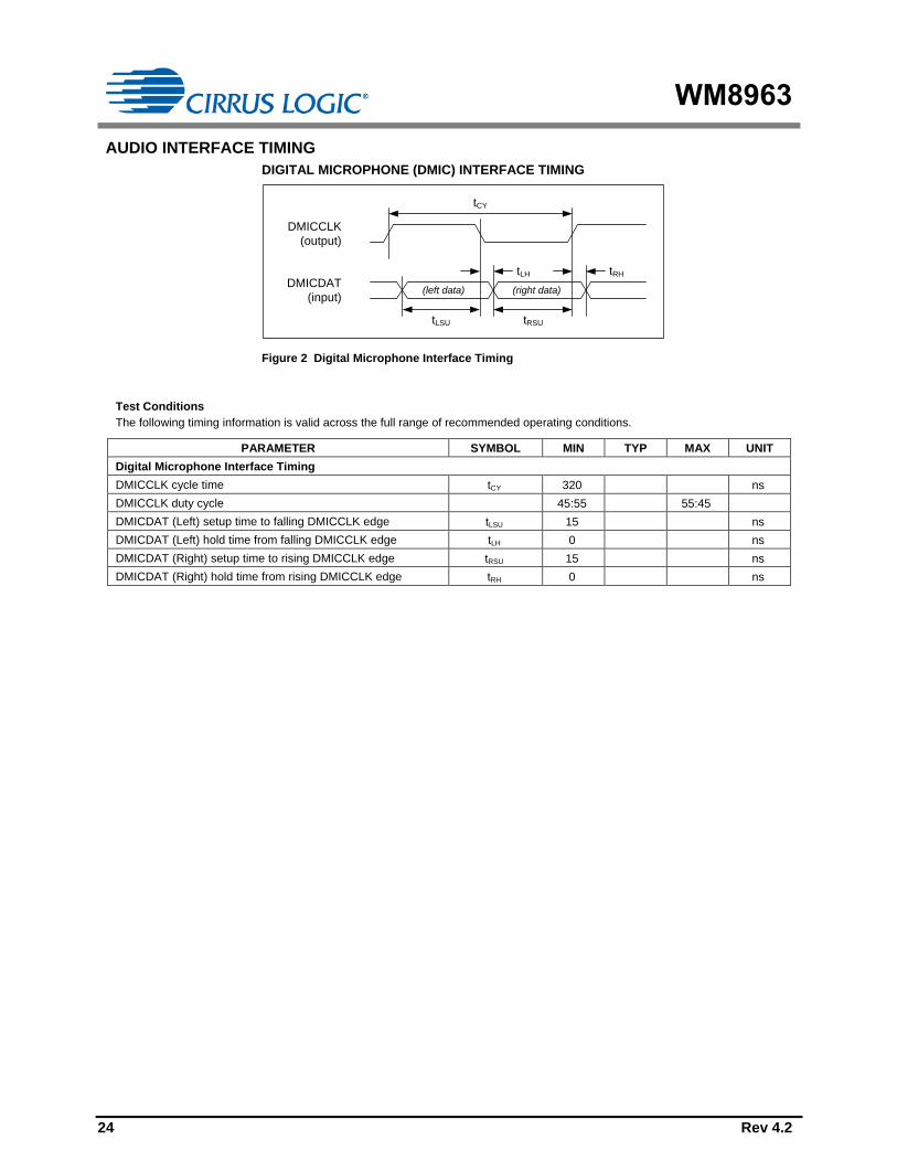
AUDIO INTERFACE TIMING
DIGITAL MICROPHONE (DMIC) INTERFACE TIMING
DMICCLK
(output)
DMICDAT
(input)
tCY
tLH tRH
tLSU tRSU
(left data) (right data)
Figure 2 Digital Microphone Interface Timing
Test Conditions
The following timing information is valid across the full range of recommended operating conditions.
PARAMETER SYMBOL MIN TYP MAX UNIT
Digital Microphone Interface Timing
DMICCLK cycle time tCY 320 ns
DMICCLK duty cycle 45:55 55:45
DMICDAT (Left) setup time to falling DMICCLK edge tLSU 15 ns
DMICDAT (Left) hold time from falling DMICCLK edge tLH 0 ns
DMICDAT (Right) setup time to rising DMICCLK edge tRSU 15 ns
DMICDAT (Right) hold time from rising DMICCLK edge tRH 0 ns

WM8963
Rev 4.2 25
DIGITAL AUDIO INTERFACE - MASTER MODE
BCLK (Output)
ADCDAT
LRCLK (Output)
tDL
DACDAT
tDDA
tDHT
tDST
Figure 3 Audio Interface Timing - Master Mode
Test Conditions
The following timing information is valid across the full range of recommended operating conditions.
PARAMETER SYMBOL MIN TYP MAX UNIT
Audio Interface Timing - Master Mode
LRCLK propagation delay from BCLK falling edge tDL 10 ns
ADCDAT propagation delay from BCLK falling edge tDDA 14 ns
DACDAT setup time to BCLK rising edge tDST 10 ns
DACDAT hold time from BCLK rising edge tDHT 10 ns

WM8963
26 Rev 4.2
DIGITAL AUDIO INTERFACE - SLAVE MODE
BCLK (input)
LRCLK (input)
ADCDAT (output)
DACDAT (input)
tDS
tDD
tDH
tLRH tLRSU
tBCH tBCL
tBCY
Figure 4 Audio Interface Timing – Slave Mode
Test Conditions
The following timing information is valid across the full range of recommended operating conditions.
PARAMETER SYMBOL MIN TYP MAX UNIT
Audio Interface Timing - Slave Mode
BCLK cycle time tBCY 50 ns
BCLK pulse width high tBCH 20 ns
BCLK pulse width low tBCL 20 ns
LRCLK set-up time to BCLK rising edge tLRSU 16 ns
LRCLK hold time from BCLK rising edge tLRH 10 ns
DACDAT hold time from BCLK rising edge tDH 10 ns
ADCDAT propagation delay from BCLK falling edge tDD 14 ns
DACDAT set-up time to BCLK rising edge tDS 10 ns
Note:
BCLK period should always be greater than or equal to MCLK period.

WM8963
Rev 4.2 27
DIGITAL AUDIO INTERFACE - TDM MODE
In TDM mode, it is important that two devices do not attempt to drive the ADCDAT pin simultaneously.
The timing of the WM8963 ADCDAT pin tri-stating at the start and end of the data transmission is
described below.
BCLK
ADCDAT
ADCDAT set-up time ADCDAT release time
ADCDAT undriven (tri-state) ADCDAT valid (CODEC output) ADCDAT valid ADCDAT undriven (tri-state)
Figure 5 Audio Interface Timing – TDM Mode
Test Conditions
The following timing information is valid across the full range of recommended operating conditions.
PARAMETER SYMBOL MIN TYP MAX UNIT
Audio Interface Timing - TDM Mode
ADCDAT setup time from BCLK falling edge 4 ns
ADCDAT release time from BCLK falling edge 25 ns

WM8963
28 Rev 4.2
CONTROL INTERFACE TIMING
2-WIRE (I2C) CONTROL MODE
SCLK
(input)
SDA
t4 t3
START
t8
STOPt2t1
t7
t6
t5 t9 t10
Figure 6 Control Interface Timing - 2-wire (I2C) Control Mode
Test Conditions
The following timing information is valid across the full range of recommended operating conditions.
PARAMETER SYMBOL MIN TYP MAX UNIT
Program Register Input Information
SCLK Frequency 526 kHz
SCLK Low Pulse-Width t1 1.3 us
SCLK High Pulse-Width t2 600 ns
Hold Time (Start Condition) t3 600 ns
Setup Time (Start Condition) t4 600 ns
SDA, SCLK Rise Time t6 300 ns
SDA, SCLK Fall Time t7 300 ns
Setup Time (Stop Condition) t8 600 ns
SDA Setup Time (data input) t5 100 ns
SDA Hold Time (input/output) t9 0 ns
SDA Valid Time (data/ACK output) t10 900 ns
Pulse width of spikes that will be suppressed tps 0 5 ns

WM8963
Rev 4.2 29
3-WIRE (SPI) CONTROL MODE
CS
(input)
SCLK
(input)
SDA
(input)
tCSU
tSCH tSCL
tSCY
tDHO
tDSU
tCHO
Figure 7 Control Interface Timing - 3-wire (SPI) Control Mode (Write Cycle)
SCLK
(input)
SDA
(output)
tDL
CS
(input)
Figure 8 Control Interface Timing - 3-wire (SPI) Control Mode (Read Cycle)
Test Conditions
The following timing information is valid across the full range of recommended operating conditions.
PARAMETER SYMBOL MIN TYP MAX UNIT
CS¯¯ falling edge to SCLK rising edge tCSU 40 ns
SCLK falling edge to CS¯¯ rising edge tCHO 10 ns
SCLK pulse cycle time tSCY 200 ns
SCLK pulse width low tSCL 80 ns
SCLK pulse width high tSCH 80 ns
SDA to SCLK set-up time tDSU 40 ns
SDA to SCLK hold time tDHO 10 ns
Pulse width of spikes that will be suppressed tps 0 5 ns
SCLK falling edge to SDA output transition tDL 40 ns

WM8963
30 Rev 4.2
4-WIRE (SPI) CONTROL MODE
CS
(input)
SCLK
(input)
SDA
(input)
tCSU
tSCH tSCL
tSCY
tDHO
tDSU
tCHO
Figure 9 Control Interface Timing - 4-wire (SPI) Control Mode (Write Cycle)
SCLK
(input)
SDOUT
(output)
tDL
CS
(input)
Figure 10 Control Interface Timing - 4-wire (SPI) Control Mode (Read Cycle)
Test Conditions
The following timing information is valid across the full range of recommended operating conditions.
PARAMETER SYMBOL MIN TYP MAX UNIT
CS¯¯ falling edge to SCLK rising edge tCSU 40 ns
SCLK falling edge to CS¯¯ rising edge tCHO 10 ns
SCLK pulse cycle time tSCY 200 ns
SCLK pulse width low tSCL 80 ns
SCLK pulse width high tSCH 80 ns
SDA to SCLK set-up time tDSU 40 ns
SDA to SCLK hold time tDHO 10 ns
Pulse width of spikes that will be suppressed tps 0 5 ns
SCLK falling edge to SDOUT transition tDL 40 ns

WM8963
Rev 4.2 31
POWER ON RESET TIMING
The WM8963 includes an internal Power-On-Reset (POR) circuit, which is used to reset the digital
logic into a default state after power up. The POR circuit is powered from AVDD and monitors
DCVDD. The internal POR¯¯¯ signal is asserted low when AVDD and DCVDD are below minimum
thresholds.
The specific behaviour of the circuit will vary, depending on the relative timing of the supply voltages.
Typical scenarios are illustrated in Figure 11 and Figure 12.
DCVDD
Vpord_on
0V
AVDD
0V
Vpora
Vpora_off
LO
HI
Internal POR
Device readyPOR active POR active
POR undefined
Figure 11 Power On Reset Timing - AVDD enabled first
DCVDD
0V
AVDD
0V
Vpora
Vpord_off
LO
HI
Internal POR
Device ready
Vpora_on
POR active POR active
POR undefined
Figure 12 Power On Reset Timing - DCVDD enabled first

WM8963
32 Rev 4.2
The POR¯¯¯ signal is undefined until AVDD has exceeded the minimum threshold, Vpora Once this
threshold has been exceeded, POR¯¯¯ is asserted low and the chip is held in reset. In this condition, all
writes to the control interface are ignored. Once AVDD and DCVDD have reached their respective
power on thresholds, POR¯¯¯ is released high, all registers are in their default state, and writes to the
control interface may take place.
Note that a minimum power-on reset period, TPOR, applies even if AVDD and DCVDD have zero rise
time. (This specification is guaranteed by design rather than test.)
On power down, POR¯¯¯ is asserted low when any of AVDD or DCVDD falls below their respective
power-down thresholds.
Typical Power-On Reset parameters for the WM8963 are defined in Table 1.
SYMBOL DESCRIPTION TYP UNIT
Vpora AVDD threshold below which POR is undefined 0.5 V
Vpora_on Power-On threshold (AVDD) 1.1 V
Vpora_off Power-Off threshold (AVDD) 1.1 V
Vpord_on Power-On threshold (DCVDD) 0.9 V
Vpord_off Power-Off threshold (DCVDD) 0.65 V
TPOR Minimum Power-On Reset period 9.5 s
Table 1 Typical Power-On Reset Parameters
Notes:
1. If AVDD and DCVDD suffer a brown-out (i.e. drop below the minimum recommended operating
level but do not go below Vpora_off or Vpord_off) then the chip does not reset and resumes normal
operation when the voltage is back to the recommended level again.
2. The chip enters reset at power down when AVDD or DCVDD falls below Vpora_off or Vpord_off. This
may be important if the supply is turned on and off frequently by a power management system.
3. The minimum TPOR period is maintained even if DCVDD and AVDD have zero rise time. This
specification is guaranteed by design rather than test.

WM8963
Rev 4.2 33
DEVICE DESCRIPTION
INTRODUCTION
The WM8963 is a low power audio CODEC offering a combination of high quality audio, advanced
features, low power and small size. These characteristics make it ideal for portable digital audio
applications with stereo speaker and headphone outputs such as games consoles, portable media
players and multimedia phones.
A flexible input configuration supports a single-ended stereo microphone interface and a digital
microphone interface. A boost amplifier is available for additional gain on the analogue microphone
inputs. A programmable gain amplifier (PGA) with an automatic level control (ALC) function can be
used to maintain a constant microphone recording volume.
Stereo class D speaker drivers can provide up to 2W per channel into 4 BTL loads. It is also
possible to configure the speaker drivers as a mono output, giving enhanced performance.
Highly flexible output speaker boost settings provide fully internal level-shifting of analogue output
signals, allowing speaker output power to be maximised while minimising other analogue supply
currents, and requiring no additional components.
A dual mode (Level Shifting or Inverting Mode) charge pump generates split supplies for the
headphone output amplifiers allowing these to be ground referenced.
A DC servo to remove offsets from the headphone outputs, low leakage and a user controlled power-
up/power-down Control Sequencer provides powerful pop and click suppression mechanisms which
enable direct battery connection. These anti-pop/click mechanisms, and no requirement for any
external DC blocking capacitors to the headphone, results in a reduced external component count and
reduced power consumption in portable battery-powered applications.
The hi-fi quality stereo ADC and DAC uses a 24-bit, low-order over-sampling architecture to deliver
optimum performance. ADC and DAC operate at the same sample rate.
The integrated audio enhancement DSP provides powerful benefits in audio processing. Virtual
Surround Sound (VSS) widens the stereo speaker audio image, and ReTuneTM can be used to flatten
the frequency response of an external speaker. The Multi-band Compressor (MBC) can maximize the
loudness of an audio signal, without overdriving the speaker. Further audio enhancements are
provided in a fixed function, configurable DSP; these include 3D widening for recording, a 5-band
parametric EQ, and a Dynamic Range Controller.
The WM8963 has a highly flexible digital audio interface, supporting a number of protocols, including
I2S, DSP, MSB-first left/right justified, and can operate in master or slave modes. PCM operation is
supported in the DSP mode. A-law and -law companding are also supported. Time division
multiplexing (TDM) is available to allow multiple devices to stream data simultaneously on the same
bus, saving space and power.
The internal system clock (SYSCLK) can be derived from an external clock input, or from the
integrated crystal oscillator. A Frequency Locked Loop (FLL) is available to support flexible clocking
configurations. All MCLK frequencies typically used in portable systems are supported for sample
rates between 8kHz and 96kHz. The ADC and DAC must be configured to operate at the same
sample rate. A flexible switching clock for the class D speaker drivers (synchronous with the audio
DSP clocks for best performance) is also derived from SYSCLK.
The WM8963 can generate outputs from the FLL or crystal oscillator, to provide clocking for external
circuits. General purpose output functions (eg. clock, interrupt, and status flags) are also supported on
up to three GPIO pins.
To allow full software control over all its features, the WM8963 supports 2-wire (I2C) and 3- or 4-wire
(SPI) serial control interface modes, with full read-back capability on all registers. The WM8963 is fully
compatible with, and an ideal partner to, a wide range of industry standard microprocessors,
controllers and DSPs. Unused functions can be disabled via software to save power, while low
leakage currents extend standby and off time in portable battery-powered applications.

WM8963
34 Rev 4.2
INPUT SIGNAL PATH
The WM8963 has many analogue input channels, configurable in any combination of up to eight mono
or four stereo inputs.
Any of the analogue inputs may be connected to the input PGA on the associated left or right channel.
(Note that only one analogue input can be connected to the PGA at any time; the PGA does not
perform any signal mixing.)
The left and right analogue inputs IN2 and IN3 can be connected to the input boost mixer on the
associated left or right channel, bypassing the input PGA.
Note that the input signal path audio performance is affected by the choice of signal path. Best
performance is achieved using analogue inputs IN2 or IN3 connected directly to the input boost mixer.
The performance of the input signal paths are ranked as described in the list below (best performance
first).
IN2 or IN3 connected directly to the input boost mixer
IN1 or IN4 connected via the input PGA
IN2 or IN3 connected via the input PGA
The left and right analogue inputs IN4 can be connected directly to the output signal mixers, which
drive the headphone or speaker outputs.
The input signal paths and the control registers are shown in Figure 13.
IN1R
IN4R
+
+
ADC
DIGITAL
FILTERS
ALC
Wind noise
Filter
Volume
INPGAL_ENA
or
INL_ENA
INPGAR_ENA
or
INR_ENA
PGAL
PGARIN1R_TO_INPGAR
IN4R_TO_INPGAR
INL_VOL
IN_VU
INL_ZC
INPGAL_MUTE
INR_VOL
IN_VU
INR_ZC
INPGAR_MUTE
MIXINL
MIXINL_ENA
or
INL_ENA
MIXINR_ENA
or
INR_ENA
MIXINR_MUTE
ADC
ADCINPGAL_TO_MIXINL / INPGAL_MIXINL_VOL
INPGAR_TO_MIXINR / INPGAR_MIXINR_VOL
VMID
VMID
IN2R
IN3R
IN2R_TO_INPGAR
IN3R_TO_INPGAR
IN1L
IN4L
IN1L_TO_INPGAL
IN4L_TO_INPGAL
IN2L
IN3L
IN2L_TO_INPGAL
IN3L_TO_INPGAL
IN3R_TO_MIXINR / IN3R_MIXINR_VOL
IN2R_TO_MIXINR / IN2R_MIXINR_VOL
To Left and Right Output Mixers
To Left and Right Output Mixers
IN2L_TO_MIXINL / IN2L_MIXINL_VOL
IN3L_TO_MIXINL / IN3L_MIXINL_VOL
MIXINL_MUTE
MIXINR
+
+
Figure 13 Analogue Input Signal Path

WM8963
Rev 4.2 35
MICROPHONE INPUT CONNECTION
The WM8963 supports analogue and digital microphone input. Refer to the “Digital Microphone
Interface” section for details of the digital microphone input.
The input PGAs use single-ended or pseudo-differential connections, depending on the selected input
pin. A microphone bias generator is provided, suitable for powering electret condenser microphones.
Single-ended analogue microphone input using IN1L, IN1R, IN4L or IN4R is configured as shown in
Figure 14.
MICBIAS
MIC
GND
To input mixer
VMID
IN1L, IN4L,
IN1R, IN4R
+
-
PGA
Figure 14 Microphone Input IN1 or IN4
Pseudo-differential microphone input, using IN2L, IN2R, IN3L or IN3R as an input to the PGA, is
configured as shown in Figure 15. The inverting (or ‘noisy ground’) signal is connected to the
respective IN1 pin (IN1L or IN1R), using an external capacitor, as shown.
When IN2L, IN2R, IN3L or IN3R is selected as an input to the PGA (using the register bits described
in Table 5), the respective IN1 pin (IN1L or IN1R) is automatically connected to the PGA in order to
support the capacitor requirement described above.
MICBIAS
MIC
GND
To input mixer
IN2L, IN3L,
IN2R, IN3R
-
+
PGAIN1L, IN1R
GND
Figure 15 Microphone Input IN2 or IN3
LINE INPUT CONNECTION
Single-ended line inputs may be connected to the left or right channel analogue inputs IN1, IN2, IN3
or IN4, and routed to the input mixers or output signal paths as illustrated in Figure 13.
Note that, if IN2L, IN2R, IN3L or IN3R is selected as an input to the PGA, then the PGA is
automatically configured in pseudo-differential mode, and the respective IN1 pin (IN1L or IN1R) must
be connected to ground via an external capacitor, as shown in Figure 15.

WM8963
36 Rev 4.2
MICROPHONE BIAS CONTROL
The WM8963 incorporates a MICBIAS generator, which provides low noise reference voltages
suitable for biasing electret condenser (ECM) type microphones via an external resistor. The input
connection to the MICBIAS generator is via the MICVDD pin.
The WM8963 also provides an LDO regulator, which can be used to generate a suitable MICVDD
supply for the MICBIAS generator. The LDO supply is provided via the LDOVDD pin. The LDO input is
suitable for direct connection to a battery.
The LDO and MICBIAS circuits are illustrated in Figure 16. Refer to the “Applications Information”
section for the recommended external connections and components.
MICBIASMICBIAS_ENA
MICBIAS_EVR
MICBIAS_LVL
LDOVDD
LDO_VOUT_SEL
LDO_OUT_FLT
LDO_ENA
MICVDD
LDO
Figure 16 LDO and MICBIAS
The LDO is enabled using the LDO_ENA register bit.
When the LDO is enabled, the MICVDD voltage can be selected using the LDO_VOUT_SEL bit. The
LDOVDD supply voltage must be at least 250mV higher than the desired MICVDD output voltage.
When the LDO is disabled, the MICVDD pin can be configured to be floating or to be actively
discharged. This is selected using the LDO_OUT_FLT register bit.
When the LDO is used to generate the MICVDD supply, there should be no external connections to
the MICVDD pin. Note that, in this configuration, the MICVDD must not be left floating at any time; the
LDO_OUT_FLT register bit should be set to ‘0’ in this case.
If the LDO is not used, then the MICVDD and LDOVDD pins should be tied together, and connected
to a suitable MICVDD supply. Under these conditions, the default LDO register settings must be used
(LDO_ENA=0, LDO_OUT_FLT=1).
The MICBIAS generator is powered from MICVDD, which can be supplied internally or externally, as
described above.
The MICBIAS output is enabled using the MICBIAS_ENA register bit. The MICBIAS voltage is
selected using the MICBIAS_LVL and MICBIAS_EVR register fields, as detailed in Table 2.
The MICVDD voltage must be at least 300mV higher than the desired MICBIAS output voltage. If the
LDO is used to generate the MICVDD supply, the minimum MICVDD requirement can be reduced to
250mV above the desired MICBIAS output voltage.
Note that an external decoupling capacitor is required on the MICBIAS output. A suitable capacitor
must be connected whenever the MICBIAS output is enabled. Additional filtering of the MICBIAS
output, to reduce noise and interference, may be implemented as described in the “Applications
Information” section, if required.

WM8963
Rev 4.2 37
REGISTER
ADDRESS
BIT LABEL DEFAULT DESCRIPTION
R25 (19h)
Pwr Mgmt
(1)
1 MICBIAS_ENA 0 Microphone Bias Enable
0 = OFF (high impedance output)
1 = ON
R29 (1Dh)
Micbias
1:0 MICBIAS_EVR
[1:0]
00 Microphone Bias Voltage Control
00 = Controlled by MICBIAS_LVL
10 = 1.34 x AVDD (approx.)
X1 = 1.63 x AVDD (approx.)
R48 (30h)
MICBIAS
0 MICBIAS_LVL 1 Microphone Bias Voltage Control
0 = 0.828 x AVDD (approx.)
1 = 1.156 x AVDD (approx.)
Only valid when MICBIAS_EVR=00. In
other cases, the Microphone Bias voltage
is controlled by MICBIAS_EVR alone.
R176
(B0h)
LDO
2 LDO_VOUT_SEL 0 LDO output voltage level setting.
0 = 1.36 x AVDD
1 = 1.78 x AVDD
1 LDO_OUT_FLT 1 LDO Output Float setting, effective when
LDO_ENA==0
0 = LDO output is clamped to ground
1 = LDO output is floating (default)
0 LDO_ENA 0 LDO Enable
0 = Disabled (default)
1 = Enabled
Table 2 Microphone Bias Control
Note that the maximum source current capability for MICBIAS is 2.0mA. The external biasing
resistance must be large enough to limit the MICBIAS current to 2.0mA across the full microphone
impedance range.
MICBIAS CURRENT DETECT
A MICBIAS Current Detect function is provided for external accessory detection. This is provided in
order to detect the insertion/removal of a microphone or the pressing/releasing of the microphone
‘hook’ switch; these events will cause a significant change in MICBIAS current flow, which can be
detected and used to generate a signal to the host processor.
The MICBIAS current detect function is enabled by setting the MICDET_ENA register bit. When this
function is enabled, two current thresholds can be defined, using the MICDET_THR and
MICSHORT_THR registers. When a change in MICBIAS current which crosses either threshold is
detected, then an interrupt event can be generated. In a typical application, accessory insertion would
be detected when the MICBIAS current exceeds MICDET_THR, and microphone hookswitch
operation would be detected when the MICBIAS current exceeds MICSHORT_THR.
The current detect threshold functions are both inputs to the Interrupt control circuit and can be used
to trigger an Interrupt event when either threshold is crossed. The status flags MICDET_STS or
MICSHORT_STS are asserted whenever the relevant current threshold is exceeded.
The current detect thresholds are enabled and controlled using the registers described in Table 3
Performance parameters for this circuit block can be found in the “Electrical Characteristics” section.
Filtering is also provided in both current detect circuits to improve reliability in conditions where AC
current spikes are present due to ambient noise conditions. This feature is described in the following
section. Further guidance on the usage of the MICBIAS current monitoring features is also described
in the following pages.

WM8963
38 Rev 4.2
REGISTER
ADDRESS
BIT LABEL DEFAULT DESCRIPTION
R48 (30h)
Additional
Control (4)
14:12 MICDET_THR [2:0] 000 MICBIAS Current Detect Threshold
(AVDD = 1.8V)
000 = 64uA
001 = 166uA
010 = 358uA
011 = 461uA
100 = 563uA
101 = 666uA
110 = 858uA
111 = 960uA
Note that the value scales with
AVDD. The value quoted is correct
for AVDD=1.8V.
11:10 MICSHORT_THR
[1:0]
00 MICBIAS Short Circuit Threshold
(AVDD = 1.8V)
00 = 510uA
01 = 653uA
10 = 1040uA
11 = 1200uA
Note that the value scales with
AVDD. The value quoted is correct
for AVDD=1.8V.
9 MICDET_ENA 0 MICBIAS Current and Short Circuit
Detect Enable
0 = Disabled
1 = Enabled
7 MICDET_STS 0 MICBIAS Current Detection status
0 = Current Detect threshold not
exceeded
1 = Current Detect threshold
exceeded
6 MICSHORT_STS 0 MICBIAS Short Circuit status
0 = Short Circuit threshold not
exceeded
1 = Short Circuit threshold
exceeded
Table 3 MICBIAS Current Detect

WM8963
Rev 4.2 39
MICBIAS CURRENT DETECT FILTERING
The function of the filtering is to ensure that AC current spikes caused by ambient noise conditions
near the microphone do not lead to incorrect signalling of the microphone insertion/removal status or
the microphone hookswitch status.
Digital filtering of the hookswitch status ensures that the MICBIAS Short Circuit detection event is only
signalled if the MICSHORT_THR threshold condition has been met for 10 consecutive measurements.
In a typical application, microphone insertion would be detected when the MICBIAS current exceeds
the Current Detect threshold set by MICDET_THR.
When the MICD_IRQ_POL interrupt polarity bit is set to 0, then microphone insertion detection will
cause the MICD_EINT interrupt status register to be set. (See “Interrupts” for details of these register
bits.)
For detection of microphone removal, the MICD_IRQ_POL bit should be set to 1. When the
MICD_IRQ_POL interrupt polarity bit is set to 1, then microphone removal detection will cause the
MICD_EINT interrupt status register to be set.
The detection of these events is bandwidth limited for best noise rejection, and is subject to detection
delay time tDET, as specified in the “Electrical Characteristics” section. Provided that the MICDET_THR
field has been set appropriately, each insertion or removal event is guaranteed to be detected within
the delay time tDET.
It is likely that the microphone socket contacts will have mechanical “bounce” when a microphone is
inserted or removed, and hence the resultant control signal will not be a clean logic level transition.
Since tDET has a range of values, it is possible that the interrupt will be generated before the
mechanical “bounce” has ceased. Hence after a mic insertion or removal has been detected, a time
delay should be applied before re-configuring the MICD_IRQ_POL bit. The maximum possible
mechanical bounce times for mic insertion and removal must be understood by the software
programmer.
Microphone hook switch operation is detected when the MICBIAS current exceeds the Short Circuit
Detect threshold set by MICSHORT_THR. Using the digital filtering, the hook switch detection event is
only signalled if the MICSHORT_THR threshold condition has been met for 10 consecutive
measurements.
When the MICSCD_IRQ_POL interrupt polarity bit is set to 0, then hook switch operation will cause
the MICSCD_EINT interrupt status register to be set. (See “Interrupts” for details of these register
bits.)
For detection of microphone removal, the MICSCD_IRQ_POL bit should be set to 1. When the
MICSCD_IRQ_POL interrupt polarity bit is set to 1, then hook switch release will cause the
MICSCD_EINT interrupt status register to be set.
The hook switch detection measurement frequency and the detection delay time tSHORT are detailed in
the “Electrical Characteristics” section.
The WM8963 Interrupt function is described in the “Interrupts” section. Example control sequences for
configuring the Interrupts functions for MICBIAS current detection events are described in the
“Applications Information”section.
A clock is required for the digital filtering function. This requires:
MCLK is present or the FLL is selected as the SYSCLK source in free-running mode
SYSCLK_ENA = 1
Any MICBIAS Current Detect event (accessory insertion/removal or hookswitch press/release) which
happens while one or more of the clocking criteria is not satisfied (for example during a low power
mode where the CPU has disabled MCLK) will still be detected, but only after the clocking conditions
are met. An example is illustrated in Figure 17, where the mic is inserted while MCLK is stopped.
Note that the interrupts and digital filtering can be supported in the absence of an external clock by
using the FLL in free-running mode and selecting the FLL as the clock source, as described in
“Clocking and Sample Rates”.

WM8963
40 Rev 4.2
MCLK
Mic insertion event
IRQ
(1) insertion event
happens at any time
during this period
(2) insertion indicated tDET
after MCLK re-started
tDET
Figure 17 MICBIAS Detection Events without MCLK
MICROPHONE HOOK SWITCH DETECTION
The possibility of spurious hook switch interrupts due to ambient noise conditions can be removed by
detailed understanding of microphone behaviour under extremely high sound pressure levels or
during mechanical shock, and by correct selection of the MICBIAS resistor value; these factors will
affect the level of the MICBIAS AC current spikes.
In applications where the Current Detect threshold is close to the level of the current spikes, the
probability of false detections is reduced by the digital filtering described above.
Note that the filtering algorithm provides only limited rejection of very high current spikes at
frequencies less than or equal to the hook switch detect measurement frequency, or at frequencies
equal to harmonics of the hook switch detect measurement frequency.
The MICBIAS Hook Switch detection filtering is illustrated in Figure 18. Example control sequences for
configuring the Interrupts functions for MICBIAS current detection events are described in the
““Applications Information”section.
10x sampling circuit
MIC
BIA
S
cu
rre
nt
Hook switch
threshold
No interrupt
event
Interrupt event due to
threshold exceeded for
10 successive samples
Time
10x sampling circuit
tSHORT
Extreme current
spikes caused by
high sound pressure
such as wind noise
Hook switch pressed
tSHORT
Figure 18 MICBIAS Hook Switch Detection Filtering

WM8963
Rev 4.2 41
INPUT PGA ENABLE
The input PGAs (Programmable Gain Amplifiers) are enabled using register bits INL_ENA, INR_ENA,
INPGAR_ENA and INPGAL_ENA, as described in Table 4.
These PGAs provide adjustable gain control from -23.25dB to +24.0dB in 0.75dB increments as
shown in Table 7.
REGISTER
ADDRESS
BIT LABEL DEFAULT DESCRIPTION
R25 (19h)
Pwr Mgmt (1)
5 INL_ENA 0 Left Input PGA and Mixer Enable.
0 = Disabled
1 = Enabled
4 INR_ENA 0 Right Input PGA and Mixer Enable.
0 = Disabled
1 = Enabled
R37 (25h)
Left Input PGA
Control
4 INPGAL_ENA 0 Left Input PGA Enable.
0 = Disabled
1 = Enabled
Note that the Left Input PGA is also
enabled when INL_ENA is set
R38 (26h)
Right Input
PGA Control
4 INPGAR_ENA 0 Right Input PGA Enable
0 = Disabled
1 = Enabled
Note that the Right Input PGA is
also enabled when INR_ENA is set
Table 4 Input PGA Enable
To enable the input PGAs, the reference voltage VMID and the bias current must also be enabled.
See “Reference Voltages and Bias Control” for details of the associated controls VMID_SEL and
BIAS_ENA.

WM8963
42 Rev 4.2
INPUT PGA CONFIGURATION
Each of the PGAs operates in a single-ended mode. Configuration of the PGA inputs to the WM8963
input pins is controlled using the register bits shown in Table 5.
The maximum available attenuation on any of these input paths is achieved by using register bits
shown in Table 5 to disconnect the input pins from the applicable PGA.
REGISTER
ADDRESS
BIT LABEL DEFAULT DESCRIPTION
R37 (25h)
Left input
PGA control
3 IN1L_TO_INPGAL 1 Selects the IN1L pin as an input to the
Left PGA
0 = Disabled
1 = Enabled
2 IN2L_TO_INPGAL 0 Selects the IN2L pin as an input to the
Left PGA
0 = Disabled
1 = Enabled
1 IN3L_TO_INPGAL 0 Selects the IN3L pin as an input to the
Left PGA
0 = Disabled
1 = Enabled
0 IN4L_TO_INPGAL 0 Selects the IN4L pin as an input to the
Left PGA
0 = Disabled
1 = Enabled
R38 (26h)
Right input
PGA control
3 IN1R_TO_INPGA
R
1 Selects the IN1R pin as an input to the
Right PGA
0 = Disabled
1 = Enabled
2 IN2R_TO_INPGA
R
0 Selects the IN2R pin as an input to the
Right PGA
0 = Disabled
1 = Enabled
1 IN3R_TO_INPGA
R
0 Selects the IN3R pin as an input to the
Right PGA
0 = Disabled
1 = Enabled
0 IN4R_TO_INPGA
R
0 Selects the IN4R pin as an input to the
Right PGA
0 = Disabled
1 = Enabled
Table 5 Input PGA Configuration
INPUT PGA VOLUME CONTROL
Each of the two Input PGAs has an independently controlled gain range of -23.25dB to +24dB in
0.75dB steps. Each Input PGA can be independently muted using the PGA mute bits as described in
Table 6, with maximum mute attenuation achieved by simultaneously disabling the corresponding
inputs described in Table 5.
To prevent "zipper noise", a zero-cross function is provided on the input PGAs. When this feature is
enabled, volume updates will not take place until a zero-crossing is detected. In the case of a long
period without zero-crossings, a timeout function is provided. When the zero-cross function is
enabled, the volume will update after the timeout period if no earlier zero-cross has occurred. The
timeout clock is enabled using TOCLK_ENA, the timeout period is set by TOCLK_DIV. See “Clocking
and Sample Rates” for more information on these fields.

WM8963
Rev 4.2 43
The IN_VU bits control the loading of the input PGA volume data and the PGA mute functions. When
IN_VU is set to 0, the PGA volume data will be loaded into the respective control register, but will not
actually change the gain setting. The INL and INR volume settings are both updated when a 1 is
written to either IN_VU bit. Similarly, the INPGAL_MUTE and INPGAR_MUTE settings are only
effective when a 1 is written to either IN_VU bit. This makes it possible to update the gain/mute of the
left and right signal paths simultaneously.
Note that the Input PGA control has a dependency on the correct sequencing of the ALC and ADC
Enable control registers; if the correct sequences are not followed, then the Input PGA gain settings
may become fixed. See “Automatic Level Control (ALC)” for further details.
The Input PGA Volume Control register fields are described in Table 6 and Table 7.
REGISTER
ADDRESS
BIT LABEL DEFAULT DESCRIPTION
R0 (0h)
Left input
volume
8 IN_VU N/A Input PGA Volume and Mute Update
Writing a 1 to this bit will cause the INL
and INR volume and mute settings to be
updated simultaneously
7 INPGAL_M
UTE
1 Left input PGA Mute
0 = Unmuted
1 = Muted
6 INL_ZC 0 INL PGA Zero Cross Detector
0 = Change gain immediately
1 = Change gain on zero cross only
5:0 INL_VOL
[5:0]
1Fh Left input PGA Volume
-23.25dB to +24.00dB in 0.75dB steps.
00h = -23.25dB
01h = -22.50dB
02h = -21.75dB
...(0.75dB steps)
1Fh = 0dB
…
3Fh = 24dB
See Table 7 for volume range.
R1 (1h)
Right input
volume
8 IN_VU N/A Input PGA Volume and Mute Update
Writing a 1 to this bit will cause the INL
and INR volume and mute settings to be
updated simultaneously
7 INPGAR_M
UTE
1 Right input PGA Mute
0 = Unmuted
1 = Muted
6 INR_ZC 0 INR PGA Zero Cross Detector
0 = Change gain immediately
1 = Change gain on zero cross only
5:0 INR_VOL
[5:0]
1Fh Right input PGA Volume
-23.25dB to +24.00dB in 0.75dB steps.
00h = -23.25dB
01h = -22.50dB
02h = -21.75dB
...(0.75dB steps)
1Fh = 0dB
…
3Fh = 24dB
See Table 7 for volume range.
Table 6 Input PGA Volume Control

WM8963
44 Rev 4.2
INL_VOL[5:0],
INR_VOL[5:0]
VOLUME
(dB)
INL_VOL[5:0],
INR_VOL[5:0]
VOLUME
(dB)
00h -23.25 20h 0.75
01h -22.50 21h 1.50
02h -21.75 22h 2.25
03h -21.00 23h 3.00
04h -20.25 24h 3.75
05h -19.50 25h 4.50
06h -18.75 26h 5.25
07h -18.00 27h 6.00
08h -17.25 28h 6.75
09h -16.50 29h 7.50
0Ah -15.75 2Ah 8.25
0Bh -15.00 2Bh 9.00
0Ch -14.25 2Ch 9.75
0Dh -13.50 2Dh 10.50
0Eh -12.75 2Eh 11.25
0Fh -12.00 2Fh 12.00
10h -11.25 30h 12.75
11h -10.50 31h 13.50
12h -9.75 32h 14.25
13h -9.00 33h 15.00
14h -8.25 34h 15.75
15h -7.50 35h 16.50
16h -6.75 36h 17.25
17h -6.00 37h 18.00
18h -5.25 38h 18.75
19h -4.50 39h 19.50
1Ah -3.75 3Ah 20.25
1Bh -3.00 3Bh 21.00
1Ch -2.25 3Ch 21.75
1Dh -1.50 3Dh 22.50
1Eh -0.75 3Eh 23.25
1Fh 0.00 3Fh 24.00
Table 7 Input PGA Volume Range
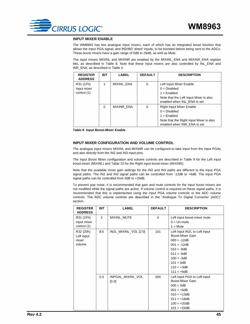
WM8963
Rev 4.2 45
INPUT MIXER ENABLE
The WM8963 has two analogue input mixers, each of which has an integrated boost function that
allows the Input PGA signal, and IN2/IN3 ‘direct’ inputs, to be boosted before being sent to the ADCs.
These boost mixers have a gain range of 0dB to 29dB, as well as Mute.
The input mixers MIXINL and MIXINR are enabled by the MIXINL_ENA and MIXINR_ENA register
bits, as described in Table 8. Note that these input mixers are also controlled by INL_ENA and
INR_ENA, as described in Table 4.
REGISTER
ADDRESS
BIT LABEL DEFAULT DESCRIPTION
R31 (1Fh)
Input mixer
control (1)
1 MIXINL_ENA 0 Left Input Mixer Enable
0 = Disabled
1 = Enabled
Note that the Left Input Mixer is also
enabled when INL_ENA is set
0 MIXINR_ENA 0 Right Input Mixer Enable
0 = Disabled
1 = Enabled
Note that the Right Input Mixer is also
enabled when INR_ENA is set
Table 8 Input Boost-Mixer Enable
INPUT MIXER CONFIGURATION AND VOLUME CONTROL
The analogue input mixers MIXINL and MIXINR can be configured to take input from the input PGAs
and also directly from the IN2 and IN3 input pins.
The Input Boost Mixer configuration and volume controls are described in Table 9 for the Left input
boost-mixer (MIXINL) and Table 10 for the Right input boost-mixer (MIXINR).
Note that the available mixer gain settings for the IN2 and IN3 paths are different to the input PGA
signal paths. The IN2 and IN3 signal paths can be controlled from -12dB to +6dB. The input PGA
signal paths can be controlled from 0dB to +29dB.
To prevent pop noise, it is recommended that gain and mute controls for the input boost mixers are
not modified while the signal paths are active. If volume control is required on these signal paths, it is
recommended that this is implemented using the input PGA volume controls or the ADC volume
controls. The ADC volume controls are described in the “Analogue To Digital Converter (ADC)”
section.
REGISTER
ADDRESS
BIT LABEL DEFAULT DESCRIPTION
R31 (1Fh)
Input mixer
control (1)
3 MIXINL_MUTE 0 Left input boost-mixer mute
0 = Un-mute
1 = Mute
R32 (20h)
Left input
mixer
volume
8:6 IN2L_MIXINL_VOL [2:0] 101 Left input IN2L to Left input
Boost-Mixer Gain
000 = -12dB
001 = -12dB
010 = -9dB
011 = -6dB
100 = -3dB
101 = 0dB
110 = +3dB
111 = +6dB
5:3 INPGAL_MIXINL_VOL
[5:3]
000 Left input PGA to Left input
Boost-Mixer Gain
000 = 0dB
001 = +6dB
010 = +13dB
011 = +18dB
100 = +20dB
101 = +24dB

WM8963
46 Rev 4.2
REGISTER
ADDRESS
BIT LABEL DEFAULT DESCRIPTION
110 = +27dB
111 = +29dB
2:0 IN3L_MIXINL_VOL [2:0] 101 Left input IN3L to Left input
Boost-Mixer Gain
000 = -12dB
001 = -12dB
010 = -9dB
011 = -6dB
100 = -3dB
101 = 0dB
110 = +3dB
111 = +6dB
R34 (22h)
Input mixer
control (2)
5 IN2L_TO_MIXINL 0 Left Input IN2L to Left input
Boost-Mixer Select
0 = Disabled
1 = Enabled
4 IN3L_TO_MIXINL 0 Left Input IN3L to Left input
Boost-Mixer Select
0 = Disabled
1 = Enabled
3 INPGAL_TO_MIXINL 1 Left Input PGA to Left input
Boost-Mixer Select
0 = Disabled
1 = Enabled
Table 9 Left Input Mixer (MIXINL) Volume Control
REGISTER
ADDRESS
BIT LABEL DEFAULT DESCRIPTION
R31 (1Fh)
Input mixer
control (1)
2 MIXINR_MUTE 0 Right input boost-mixer mute
0 = Un-mute
1 = Mute
R33 (21h)
Right input
mixer
volume
8:6 IN2R_MIXINR_VOL
[2:0]
101 Right input IN2R to Right input
Boost-Mixer Gain
000 = -12dB
001 = -12dB
010 = -9dB
011 = -6dB
100 = -3dB
101 = 0dB
110 = +3dB
111 = +6dB
5:3 INPGAR_MIXINR_VOL
[5:3]
000 Right input PGA to Right input
Boost-Mixer Gain
000 = 0dB
001 = +6dB
010 = +13dB
011 = +18dB
100 = +20dB
101 = +24dB
110 = +27dB
111 = +29dB
2:0 IN3R_MIXINR_VOL
[2:0]
101 Right input IN3R to Right input
Boost-Mixer Gain
000 = -12dB
001 = -12dB
010 = -9dB
011 = -6dB

WM8963
Rev 4.2 47
REGISTER
ADDRESS
BIT LABEL DEFAULT DESCRIPTION
100 = -3dB
101 = 0dB
110 = +3dB
111 = +6dB
R34 (22h)
Input mixer
control (2)
2 IN2R_TO_MIXINR 0 Right input IN2R to Right input
Boost-Mixer Select
0 = Disabled
1 = Enabled
1 IN3R_TO_MIXINR 0 Right input IN3R to Right input
Boost-Mixer Select
0 = Disabled
1 = Enabled
0 INPGAR_TO_MIXINR 1 Right input PGA to Right input
Boost-Mixer Select
0 = Disabled
1 = Enabled
Table 10 Right Input Mixer (MIXINR) Volume Control
AUTOMATIC LEVEL CONTROL (ALC)
The WM8963 has an automatic PGA gain control circuit that keeps a constant recording volume
irrespective of the input signal level. This is achieved by continuously adjusting the input PGA gain so
that the signal level at the ADC input remains constant.
A digital peak detector monitors the ADC output and changes the PGA gain if necessary.
The ALC has two modes selected by the ALC_MODE register. See “Limiter Mode” for further details
on the ALC Modes.
The ALC also has a Noise Gate function, which provides additional control of low level input signals.
This means that the signal path is quiet when no signal is present, giving an improvement in
background noise level.
The Automatic Level Control (ALC) can be enabled on either the left channel, or the right channel, or
on both channels, using the ALCL_ENA and ALCR_ENA fields respectively. The monitoring of the
signal is performed at the ADC. Note that the ALC (Left) function requires the Left and Right ADCs to
be enabled; the ALC (Right) function only requires the Right ADC to be enabled.
Note that, when disabling the input signal path, the ALC must be disabled before the respective ADCs
are disabled. If this sequence is not followed, then the Input PGA gain settings may become fixed.
The ALC should not be enabled when using the IN2 or IN3 inputs connected directly to the input boost
mixer; this is because these paths will bypass the PGAs where the ALC gain adjustment is performed.
ALC can be set to Active Mode or to Monitor Mode. When ALC is in Active Mode
(ALC_INACTIVE_ENA = 0), the gain of the analogue PGAs is controlled by the ALC bit settings, and
not by the INL_VOL or the INR_VOL fields. When ALC is in Monitor Mode (ALC_INACTIVE_ENA=1),
ALC monitors the signal levels without doing any of the level control that it would otherwise perform.
Details on readback of the ALC status are in the “ALC Status Readback” section.
When the ALC is enabled, a target level for the analogue input signal at the ADC is determined by the
ALC_LVL setting. There are two ranges (high or low) from which the ALC_LVL target value can be
taken. The target values in each of these ranges are shown in Table 12. Two ranges can be selected
using ALC_LVL_MODE. Set ALC_LVL_MODE to 0 to use the low range (-28.5dBFS to -6dBFS), or
set ALC_LVL_MODE to 1 to use the higher range (-22.5dBFS to -1.5dBFS).

WM8963
48 Rev 4.2
REGISTER
ADDRESS
BIT LABEL DEFAULT DESCRIPTION
R17 (11h)
ALC1
10 ALC_INACTIVE_ENA 0 Select whether the ALC is in Active
Mode (that is, ALC is controlling the
PGA gain) or in Monitor Mode (the
analogue controls are disabled). Note
that at least one of ALCL_ENA and
ALCR_ENA must also be enabled
0 = ALC is in Active Mode
1 = ALC is in Monitor Mode
9 ALC_LVL_MODE 0 Select the range of the ALC target
level.
0 = -28.5dBFS to -6dBFS in 1.5dB
steps
1 = -22.5dBFS to -1.5dBFS in 1.5dB
steps
8 ALCL_ENA 0 Select ALC on the Left channel
0 = Disabled (PGA gain set by
INL_VOL)
1 = Enabled
Note that in stereo mode, the left and
right PGA volumes, and left and right
boost mixer volumes, must be the
same before setting ALCL_ENA = 1
and ALCR_ENA = 1
7 ALCR_ENA 0 Select ALC on the Right channel
0 = Disabled (PGA gain set by
INR_VOL)
1 = Enabled
Note that in stereo mode, the left and
right PGA volumes, and left and right
boost mixer volumes, must be the
same before setting ALCL_ENA = 1
and ALCR_ENA = 1
3:0 ALC_LVL [3:0] 1011 Set the Target signal level at the
ADC input.
Note that the target level is also
determined by ALC_LVL_MODE.
ALC_LVL_MODE = 0
0000 = -28.5dBFS
0001 = -27.0dBFS
…in 1.5dB steps to…
1111 = -6dBFS
ALC_LVL_MODE = 1
0000 = -22.5dBFS
0001 = -21.0dBFS
…in 1.5dB steps to…
1110 = -1.5dBFS
1111 = -1.5dBFS
See Table 12 for the range of
possible values.
Table 11 Automatic Level Control

WM8963
Rev 4.2 49
ALC_LVL ALC_LVL_MODE = 0
(dBFS)
ALC_LVL_MODE = 1
(dBFS)
0000 -28.5 -22.5
0001 -27.0 -21.0
0010 -25.5 -19.5
0011 -24.0 -18.0
0100 -22.5 -16.5
0101 -21.0 -15.0
0110 -19.5 -13.5
0111 -18.0 -12.0
1000 -16.5 -10.5
1001 -15.0 -9.0
1010 -13.5 -7.5
1011 -12.0 -6.0
1100 -10.5 -4.5
1101 -9.0 -3.0
1110 -7.5 -1.5
1111 -6.0 -1.5
Table 12 ALC Target Level Values
LIMITER MODE
In Normal Mode (ALC_MODE = 0), the ALC will attempt to maintain a constant signal level by
increasing or decreasing the gain of the PGA. This is illustrated in Figure 19.
In Limiter Mode (ALC_MODE = 1), the ALC will reduce peaks that go above the threshold level, but
will not increase the PGA gain beyond the starting level. (The starting level is defined as the gain
setting of the PGA at the time when the ALC is enabled.) This is illustrated in Figure 20.
Note that ALC_MODE should not be changed while the ALC is active. ALCL_ENA and ALCR_ENA
must both be set to 0 before changing ALC_MODE.
REGISTER
ADDRESS
BIT LABEL DEFAULT DESCRIPTION
R19 (13h)
ALC3
8 ALC_MODE 0 ALC Mode
0 = Normal ALC Mode
1 = Limiter Mode
Note that ALCL_ENA and
ALCR_ENA must both be set to 0
before changing ALC_MODE,
otherwise unexpected behaviour
may result.
Table 13 ALC Mode Switch (ALC_MODE)

WM8963
50 Rev 4.2
Input
Signal
ALCL_ENA
ALCR_ENA
PGA
Gain
ALC_LVL
tALC_ATK tALC_DCY
Output
of PGA
PGA Gain step size (1.5dB) tALC_HLD
Figure 19 ALC Normal Mode Operation
Input
Signal
ALCL_ENA
ALCR_ENA
PGA
Gain
ALC_LVL
tALC_ATK
tALC_DCY
Output
of PGA
PGA Gainstep size (1.5dB) tALC_HLD
Figure 20 ALC Limiter Mode Operation

WM8963
Rev 4.2 51
ALC GAIN CONTROL
The minimum and maximum gain applied by the ALC is set by register fields ALC_MINGAIN and
ALC_MAXGAIN respectively. These limits can be used to alter the ALC response from that illustrated
in Figure 19 and Figure 20. If the range between maximum and minimum gain is reduced, then the
extent of the automatic level control is reduced.
Note that, when the ALC is first enabled, the PGA gain (in dB) must be less than the ALC_MAXGAIN
setting. The PGA gain is controlled by the INL_VOL and INR_VOL registers, as described in Table 6.
The minimum gain in the ALC response is set by ALC_MINGAIN. The minimum gain limit can be used
to prevent excessive attenuation of the signal path.
The maximum gain limit set by ALC_MAXGAIN can be used to prevent quiet signals (or silence) from
being excessively amplified. Note that the Noise Gate function also affects quiet signals. See the “ALC
Noise Gate” section (below) for further details on the Noise Gate.
To prevent "zipper noise", a zero-cross function is provided within the ALC. When this feature is
enabled, volume updates will not take place until a zero-crossing is detected. In the case of a long
period without zero-crossings, a timeout function is provided. When the zero-cross function is
enabled, the volume will update after the timeout period if no earlier zero-cross has occurred. The
timeout clock is enabled using TOCLK_ENA. See “Clocking and Sample Rates” for the definition of
this bit. Note that the zero-cross function can be supported without TOCLK enabled, but the timeout
function will not be provided in this case.
When operating in stereo, the peak detector takes the maximum of left and right channel peak values,
and any new gain setting is applied equally to both left and right PGAs so that the stereo image is
preserved. The input PGA and Input Mixer gain settings should be identical when entering ALC stereo
mode in order for gain updates to be applied correctly.
The ALC function can also be enabled on one channel only. In this case, only one PGA is controlled
by the ALC mechanism, while the other channel runs independently with its PGA gain set through the
control register.
When one ALC channel is unused, the peak detector disregards that channel.
REGISTER
ADDRESS
BIT LABEL DEFAULT DESCRIPTION
R17 (11h)
ALC1
6:4 ALC_MAXGAIN
[3:0]
111 Maximum ALC gain
000 = -18dB
001 = -12dB
010 = -6dB
011 = 0dB
100 = +6dB
101 = +12dB
110 = +18dB
111 = +24dB
R18 (12h)
ALC2
7 ALC_ZC 0 ALC Zero Cross Detector
0 = Change gain immediately
1 = Change gain on zero cross only
6:4 ALC_MINGAIN
[3:0]
000 Minimum ALC gain
000 = -23.25dB
001 = -17.25dB
010 = -11.25dB
011 = -5.25dB
100 = +0.75dB
101 = +6.75dB
110 = +12.75dB
111 = +18.75dB
Table 14 ALC Gain Limits

WM8963
52 Rev 4.2
ALC DYNAMIC CHARACTERISTICS
The dynamic behaviour determines how quickly the ALC responds to changing signal levels. Note that
the ALC responds to the average (RMS) signal amplitude over a period of time.
The ALC_HLD field selects a delay between the detection of a peak signal level that is below the ALC
target level, and the start of the PGA gain ramping up. ALC_HLD can be set to any of the times shown
in Table 15. ALC_HLD only affects the gain ramp-up on a low level signal. There is no delay in
ramping the gain down when the signal level is above the target level. Note that it is only the start of
the gain ramp-up that is affected by the ALC_HLD setting; once the ramp-up has started, it proceeds
at the pace dictated by the ALC_DCY setting.
The ALC_DCY field determines how quickly the ALC gain increases when the signal amplitude is low.
The times specified are for the time taken per step of applied gain. The actual time taken for the
recording level to return to its target level therefore depends on both the decay rate and the gain
adjustment required. If the required gain change is small, then the total decay time will be shorter than
when a larger gain change is required.
The ALC_ATK field determines how quickly the ALC gain decreases when the signal amplitude is
high. The times specified are for the time taken per step of applied attenuation. The actual time taken
for the recording level to return to its target level therefore depends on both the attack rate and the
gain adjustment required. If the required gain change is small, then the total decay time will be shorter
than when a larger gain change is required.
These register fields are described in Table 15.
The SAMPLE_RATE register field must be set correctly to ensure that the ALC attack, decay and hold
times are correct for the chosen sample rate. See the “Clocking and Sample Rates” section for further
details of this register.
REGISTER
ADDRESS
BIT LABEL DEFAULT DESCRIPTION
R18 (12h)
ALC2
3:0 ALC_HLD [3:0] 0000 ALC Hold time before the gain
ramp-up starts
0000 = 0.00ms
0001 = 2.67ms
0010 = 5.33ms
0011 = 10.7ms
0100 = 21.3ms
0101 = 42.7ms
0110 = 85.3ms
0111 = 171ms
1000 = 341ms
1001 = 683ms
1010 = 1.37s
1011 = 2.73s
1100 = 5.46s
1101 = 10.9s
1110 = 21.8s
1111 = 43.7s

WM8963
Rev 4.2 53
REGISTER
ADDRESS
BIT LABEL DEFAULT DESCRIPTION
R19 (13h)
ALC3
7:4 ALC_DCY [3:0] 0011 Sets the Gain Decay Rate
(measured in time per 1.5dB step).
If ALC_MODE = 0
0000 = 0.41ms / step
0001 = 0.82ms / step
…doubling with each step to…
1010 = 420ms / step
1011 = 840ms / step
1100 to 1111 = Reserved
If ALC_MODE = 1
0000 = 0.082ms / step
0001 = 0.164ms / step
…doubling with each step to…
1010 = 83.9ms / step
1011 = 168ms / step
1100 to 1111 = Reserved
Note that when 88.2kHz or 96kHz
sample rate is selected, the Gain
Decay time is defined as for the
ALC_MODE=0 case above.
See Table 16 for further details.
3:0 ALC_ATK [3:0] 0010 Sets the Gain Attack Rate
(measured in time per 1.5dB step).
If ALC_MODE = 0
0000 = 0.104ms / step
0001 = 0.208ms / step
…doubling with each step to…
1010 = 106ms / step
1011 to 1111 = Reserved
If ALC_MODE = 1
0000 = 0.020ms / step
0001 = 0.041ms / step
…doubling with each step to…
1010 = 21.0ms / step
1011 to 1111 = Reserved
Note that when 88.2kHz or 96kHz
sample rate is selected, the Gain
Attack time is defined as for the
ALC_MODE=0 case above.
See Table 17 for further details.
Table 15 ALC Time Constants

WM8963
54 Rev 4.2
ALC_DCY,
ALC_NGATE_DCY
ALC_MODE = 0 ALC_MODE = 1,
SAMPLE RATE ≤ 48kHz
ALC_MODE = 1,
SAMPLE RATE > 48kHz
0000 0.41ms 0.082ms 0.41ms
0001 0.82ms 0.164ms 0.82ms
0010 1.64ms 0.328ms 1.64ms
0011 3.28ms 0.655ms 3.28ms
0100 6.56ms 1.31ms 6.56ms
0101 13.1ms 2.62ms 13.1ms
0110 26.2ms 5.24ms 26.2ms
0111 52.5ms 10.5ms 52.5ms
1000 105ms 21.0ms 105ms
1001 210ms 41.9ms 210ms
1010 420ms 83.9ms 420ms
1011 840ms 168ms 840ms
Table 16 ALC Decay Rate (Time per 1.5dB Gain Step)
ALC_ATK,
ALC_NGATE_ATK
ALC_MODE = 0 ALC_MODE = 1,
SAMPLE_RATE ≤ 48kHz
ALC_MODE = 1,
SAMPLE RATE > 48kHz
0000 0.104ms 0.020ms 0.104ms
0001 0.208ms 0.041ms 0.208ms
0010 0.416ms 0.082ms 0.416ms
0011 0.832ms 0.164ms 0.832ms
0100 1.66ms 0.328ms 1.66ms
0101 3.33ms 0.655ms 3.33ms
0110 6.66ms 1.31ms 6.66ms
0111 13.3ms 2.62ms 13.3ms
1000 26.6ms 5.24ms 26.6ms
1001 53.2ms 10.5ms 53.2ms
1010 106ms 21.0ms 106ms
Table 17 ALC Attack Rate (Time per 1.5dB Gain Step)
PEAK LIMITER
To prevent clipping when a large signal occurs just after a period of quiet, the ALC circuit includes a
limiter function. If the ADC input signal exceeds 87.5% of full scale (–1.16dBFS), the PGA gain is
ramped down at the maximum attack rate (as when ALC_ATK = 0000), until the signal level falls
below 87.5% of full scale. This function is automatically enabled whenever the ALC is in Active Mode,
but has no effect when ALC is in Monitor Mode.
Note that if ALC_ATK = 0000, then the peak limiter makes no difference to the operation of the ALC;
ALC_ATK is already at 0000 and the ALC is therefore already ramping down at its maximum rate. The
Peak Limiter is designed to prevent clipping when long attack times are used.

WM8963
Rev 4.2 55
ALC NOISE GATE
To avoid ‘noise pumping’ when the signal is very quiet and consists mainly of noise, the ALC function
has a noise gate function. This prevents noise pumping by comparing the signal level at the input pins
against a noise gate threshold, ALC_NGATE_THR. The noise gate cuts in when:
Signal level at ADC [dB] < ALC_NGATE_THR [dB] + PGA gain [dB] + Input Mixer gain [dB]
This is equivalent to:
Signal level at input pin [dB] < ALC_NGATE_THR [dB]
Whenever the signal level at the input pins drops below the Noise Gate Threshold
(ALC_NGATE_THR), the ALC Noise Gate is activated in one of three modes. The Noise Gate Mode
is selected by ALC_NGATE_MODE. As soon as the peak input signal level drops below the Noise
Gate Threshold, control of the PGA gain is passed from the ALC to the Noise Gate system.
The Noise Gate modes are:
Mode 00: The PGA Gain remains static while the input signal is below the ALC Noise Gate
Threshold (ALC_NGATE_THR) level.
As soon as the input signal rises back above the ALC Noise Gate Threshold, PGA gain is
once again controlled by the ALC.
Mode 01: The PGA Gain is muted while the input signal is below the ALC Noise Gate
Threshold (ALC_NGATE_THR) level. The muting of the PGA Gain is immediate (a hard
mute), and is performed by setting ADCL_VOL or ADCR_VOL or both to zero. Note that
with Mode 01, it is the ADCL_VOL and ADCR_VOL registers that are muted, and not the
INL_VOL and INR_VOL registers that are changed in the other modes.
As soon as the input signal rises back above the ALC Noise Gate Threshold, ADCL_VOL
and ADCR_VOL are restored to their previous values. Again this is immediate (a hard
unmute).
Mode 10: The PGA Gain is either ramped down to the ALC_NGATE_GAIN at a rate
determined by ALC_NGATE_ATK, or ramped up to the ALC_NGATE_GAIN level at a rate
determined by ALC_NGATE_DCY.
As soon as the input signal rises back above the ALC Noise Gate Threshold, PGA gain is
once again controlled by the ALC. The PGA gain is ramped up (or down) at a rate
determined by ALC_DCY (or ALC_ATK).
The noise gate control register is described in Table 18. The ALC_NGATE_THR variable sets the
Noise Gate threshold with respect to the ADC full-scale range. The threshold is adjusted in 1.5dB
steps. Levels at the extremes of the range may cause inappropriate operation, so care should be
taken with set–up of the function. Note that the Noise Gate only works in conjunction with the ALC
function, and always operates on the same channel(s) as the ALC (left, right, both, or none).

WM8963
56 Rev 4.2
REGISTER
ADDRESS
BIT LABEL DEFAULT DESCRIPTION
R19 (13h)
ALC3
12:10 ALC_NGATE_GAIN
[2:0]
111 Noise Gate Gain level. This is the
PGA gain level used within the
ALC Noise Gate function.
000 = -23.25dB
001 = -18dB
010 = -12dB
011 = -6dB
100 = 0dB
101 = +6dB
110 = +12dB
111 = +18dB
R20 (14h)
Noise Gate
15:12 ALC_NGATE_DCY
[3:0]
0011 Sets the Noise Gate Gain Decay
Rate (time taken to ramp up to
the ALC_NGATE_GAIN level),
measured in time per 1.5dB step.
If ALC_MODE = 0
0000 = 0.41ms / step
0001 = 0.82ms / step
…doubling with each step to…
1010 = 420ms / step
1011 = 840ms / step
1100 to 1111 = Reserved
If ALC_MODE = 1
0000 = 0.082ms / step
0001 = 0.164ms / step
…doubling with each step to…
1010 = 83.9ms / step
1011 = 168ms / step
1100 to 1111 = Reserved
Note that when 88.2kHz or 96kHz
sample rate is selected, the Noise
Gate Gain Decay time is defined
as for the ALC_MODE=0 case
above.
See Table 16 for further details.
11:8 ALC_NGATE_ATK
[3:0]
0010 Sets the Gain Attack Rate (time
taken to ramp down to the
ALC_NGATE_GAIN level),
measured in time per 1.5dB step.
If ALC_MODE = 0
0000 = 0.10ms / step
0001 = 0.21ms / step
…doubling with each step to…
1010 = 106ms / step
1011 to 1111 = Reserved
If ALC_MODE = 1
0000 = 0.020ms / step
0001 = 0.041ms / step
…doubling with each step to…
1010 = 21.0ms / step
1011 to 1111 = Reserved
Note that when 88.2kHz or 96kHz
sample rate is selected, the Noise

WM8963
Rev 4.2 57
REGISTER
ADDRESS
BIT LABEL DEFAULT DESCRIPTION
Gain Attack time is defined as for
the ALC_MODE=0 case above.
See Table 17 for further details.
7:3 ALC_NGATE_THR
[4:0]
0_0000
(-76.5dBFS)
Noise Gate Threshold. If the input
signal falls below this level, the
Noise Gate function is triggered.
-76.5dB to -30dB in 1.5dB steps.
00h = -76.5dB
01h = -75.0dB
02h = -73.5dB
…(1.5dB steps)
1Eh = -31.5dB
1Fh = -30.0dB
See Table 19 for further details.
2:1 ALC_NGATE_MODE
[1:0]
00 Noise gate mode
00 = Hold PGA gain static when
noise gate triggers
01 = Mute ADC output
immediately when noise gate
triggers.
10 = Ramp PGA Gain to
ADC_NGATE_GAIN level when
Noise Gate triggers.
11 = Reserved
0 ALC_NGATE_ENA 0 Noise Gate function enable
0 = Disable
1 = Enable
Table 18 ALC Noise Gate Control

WM8963
58 Rev 4.2
ALC_NGATE_THR [4:0] THRESHOLD
(dBFS)
00h -76.5
01h -75.0
02h -73.5
03h -72.0
04h -70.5
05h -69.0
06h -67.5
07h -66.0
08h -64.5
09h -63.0
0Ah -61.5
0Bh -60.0
0Ch -58.5
0Dh -57.0
0Eh -55.5
0Fh -54.0
10h -52.5
11h -51.0
12h -49.5
13h -48.0
14h -46.5
15h -45.0
16h -43.5
17h -42.0
18h -40.5
19h -39.0
1Ah -37.5
1Bh -36.0
1Ch -34.5
1Dh -33.0
1Eh -31.5
1Fh -30.0
Table 19 ALC Noise Gate Threshold (ALC_NGATE_THR) Settings

WM8963
Rev 4.2 59
ALC STATUS READBACK
There are five ALC status registers provide monitoring of the Automatic Level Control (ALC). These
are particularly useful when ALC is in Monitor Mode (ALC_INACTIVE_ENA = 1), and the PGA Gains
are not being changed by the ALC.
These five Register bits and their settings are summarised in Table 20.
REGISTER
ADDRESS
BIT LABEL DEFAULT DESCRIPTION
R18 (12h)
ALC2
15 ALC_LOCK_ST
S
0 Readback of the ALC Lock Status.
Set when ADC signal = ALC_LVL
14 ALC_THRESH_
STS
0 Readback of the ALC Threshold
Level status (when
ALC_LOCK_STS = 0)
0 = ADC signal < ALC_LVL
1 = ADC signal > ALC_LVL
13 ALC_SAT_STS 0 Readback of the ALC saturation
status.
0 = ADC signal = ALC_LVL
1 = ADC signal < ALC_LVL but
maximum ALC Gain has been
reached
12 ALC_PKOVR_S
TS
0 Readback of the ALC Peak Limiter
Overload status.
Set when ADC input signal
exceeds -1.16dBFS
11 ALC_NGATE_S
TS
0 Readback of the ALC Noise Gate
status.
0 = ADC input signal level
> ALC_NGATE_THR
1 = ADC input signal level
< ALC_NGATE_THR
Table 20 ALC Status Readback

WM8963
60 Rev 4.2
DIGITAL MICROPHONE INTERFACE
The WM8963 supports a stereo digital microphone interface. Two channels of audio data are
multiplexed on a GPIO pin configured for digital microphone input.
The digital microphone data input (DMICDAT) is provided on GPIO5 or GPIO6 by setting the
respective GPn_FN register to 14h. The associated clock (DMICCLK) is provided on a separate GPIO
pin by setting the respective GPn_FN register to 13h. See “General Purpose Input/Output (GPIO)”
section for details on these registers.
Note that care must be taken to ensure that the respective digital logic levels of the microphone are
compatible with the digital input thresholds of the WM8963. The digital input thresholds are referenced
to DBVDD, as defined in “Electrical Characteristics”. It is recommended to power the digital
microphones from DBVDD.
When digital microphone input is enabled, the WM8963 outputs a clock signal (DMICCLK) on the
Digital Microphone Clock Output pin (this must be configured on one of the GPIO pins). The clock
frequency for all supported digital microphone clocking modes is described later in this section.
A pair of digital microphones is connected as illustrated in Figure 21. The microphones must be
configured to ensure that the Left mic transmits a data bit when DMICCLK is high, and the Right mic
transmits a data bit when DMICCLK is low. The WM8963 samples the digital microphone data at the
end of each DMICCLK phase. Each microphone must tri-state its data output when the other
microphone is transmitting.
Digital Mic
DMICDAT
0.1uF
DBVDD
DGND
Digital Mic
DMICCLK
VDD CLK DATA VDD CLK DATA
CHANCHAN
VDD
Digital
Microphone
Interface
DMICCLK is available on GPIO2, GPIO5 and GPIO6
DMICDAT is supported on GPIO5 and GPIO6
Figure 21 Digital Microphone Input
The digital microphone signal paths are enabled using the DMIC_ENA register. When DMIC_ENA is
set, the ADC path is disconnected and the digital microphone data is routed to the digital core, as
illustrated in the “Digital Mixing” section.
Two microphone channels are interleaved on DMICDAT; the timing is illustrated in Figure 22. Each
microphone must tri-state its data output when the other microphone is transmitting.

WM8963
Rev 4.2 61
DMICCLK pin
DMICDAT
(Left/Right channels
interleaved)
1 2 1 2 1 2
MIC1 output
(Left Channel)1 1 1
MIC2 output
(Right Channel)2 2 2
hi-Z
Figure 22 Digital Microphone Interface Timing
The digital microphone interface control fields are described in Table 21. Note that the ADCs must be
enabled and the sample rate must be set in order to ensure correct operation of all DSP functions
associated with the digital microphone. Volume control for the Digital Microphone Interface signals is
provided using the ADC Digital Volume Control.
See “Analogue To Digital Converter (ADC)” for details of the ADC Enable and ADC Digital Volume
control functions. See “General Purpose Input/Output (GPIO)” for details of configuring the DMICCLK
and DMICDAT functions. See “Clocking and Sample Rates” for details of the sample rate control.
REGISTER
ADDRESS
BIT LABEL DEFAULT DESCRIPTION
R25 (19h)
Pwr Mgmt (1)
10 DMIC_ENA 0 Enables Digital Microphone mode.
0 = Audio DSP input is from ADC
1 = Audio DSP input is from digital
microphone interface
Note that, when the digital
microphone interface is selected,
the ADCL_ENA and ADCR_ENA
registers must also be set to enable
the left and right digital microphone
channels respectively.
3 ADCL_ENA 0 Left ADC Enable
0 = Disabled
1 = Enabled
2 ADCR_ENA 0 Right ADC Enable
0 = Disabled
1 = Enabled
Table 21 Digital Microphone Interface Control
Note that, in addition to setting the DMIC_ENA bit as described in Table 21, the pins GPIO2, GPIO5
or GPIO6 must also be configured to provide the digital microphone interface function. See “General
Purpose Input/Output (GPIO)” for details.

WM8963
62 Rev 4.2
Clocking for the digital microphone interface is derived from SYSCLK. The DMICCLK frequency is
configured automatically, according to the SAMPLE_RATE, MCLK_RATE, and ADC_HP registers.
(See “Clocking and Sample Rates” for further details of the system clocks and control registers.)
The DMICCLK is enabled whenever a digital microphone input path is enabled on the GPIO2, GPIO5
or GPIO6 pins. Note that the SYSCLK_ENA register must also be set.
The DMICCLK frequency is as described in Table 22 (for ADC_HP=0) and Table 23 (for ADC_HP=1).
The ADC_HP bit is set to 0 by default, giving reduced power consumption.
The only valid DMICCLK configurations are the ones listed in Table 22 and Table 23. Note that some
combinations of Sample Rate and MCLK / fs ratio have a dependency on the DCVDD supply voltage.
The marked (*) combinations are only valid for DCVDD 1.7V.
The system clock, SYSCLK, must be present and enabled when using the digital microphone
interface.
SAMPLE RATE
(kHz)
MCLK RATE (MCLK / fs ratio)
256 384 512 768 1024 1536 3072 6144
8 1.024 1.024 1.024 1.024 1.024 1.024 1.024*
11.025 1.4112 1.4112 1.4112 1.4112 1.4112 1.4112*
12 1.536 1.536 1.536 1.536 1.536 1.536*
16 1.024 1.024 1.024 1.024 1.024 1.024 1.024*
22.05 1.4112 1.4112 1.4112 1.4112 1.4112 1.4112*
24 1.536 1.536 1.536 1.536 1.536 1.536*
32 2.048 2.048 2.048 2.048 2.048* 2.048*
44.1 2.8224 1.4112 2.8224 1.4112* 2.8224*
48 3.072 1.536 3.072 1.536* 3.072*
88.2 2.8224 2.8224*
96 3.072 3.072*
When ADC_HP=0, digital microphone operation is only supported for the above configurations.
Digital microphone operation is not supported for 64fs, 128fs or 192fs MCLK ratios.
Note - the configurations marked (*) are only valid for DCVDD 1.7V.
Table 22 DMICCLK Frequency (MHz) - ADC_HP = 0 (Default)
SAMPLE RATE
(kHz)
MCLK RATE (MCLK / fs ratio)
256 384 512 768 1024 1536 3072 6144
8 1.024 2.048 2.048 2.048 2.048 2.048*
11.025 1.4112 2.8224 2.8224
12 1.536 3.072 3.072
16 2.048 2.048 2.048 2.048 2.048*
22.05 2.8224 2.8224 2.8224
24 3.072 3.072 3.072
32 2.048 2.048 2.048*
44.1 2.8224 2.8224 2.8224*
48 3.072 3.072 3.072*
88.2 2.8224 2.8224*
96 3.072 3.072*
When ADC_HP=1, digital microphone operation is only supported for the above configurations.
Digital microphone operation is not supported for 64fs, 128fs or 192fs MCLK ratios.
Note - the configurations marked (*) are only valid for DCVDD 1.7V.
Table 23 DMICCLK Frequency (MHz) - ADC_HP = 1

WM8963
Rev 4.2 63
ANALOGUE TO DIGITAL CONVERTER (ADC)
The WM8963 uses stereo 24-bit, 128x oversampled sigma-delta ADCs. The use of multi-bit feedback
and high oversampling rates reduces the effects of jitter and high frequency noise. The ADC full scale
input level is proportional to AVDD - see “Electrical Characteristics”. Any input signal greater than full
scale may overload the ADC and cause distortion.
The ADCs are enabled by the ADCL_ENA and ADCR_ENA register bits. Note that when disabling the
ADC, the digital volume controls ADCL_VOL and ADCR_VOL should be muted before clearing
ADCL_ENA or ADCR_ENA to 0. This ensures that the last ADC code does not appear at the Audio
Interface (ADCDAT) pin when ADCL_ENA or ADCR_ENA are cleared.
The system clock, SYSCLK, must be configured and enabled before either of the ADCs is enabled.
See “Clocking and Sample Rates” for details of the system clocks.
Note that, when reconfiguring or disabling SYSCLK, the ADCs and DACs must be disabled before
setting SYSCLK_ENA=0.
REGISTER
ADDRESS
BIT LABEL DEFAULT DESCRIPTION
R25 (19h)
Pwr Mgmt (1)
3 ADCL_ENA 0 Left ADC Enable
0 = Disabled
1 = Enabled
2 ADCR_ENA 0 Right ADC Enable
0 = Disabled
1 = Enabled
Table 24 ADC Enable Control
ADC CLOCKING CONTROL
Clocking for the ADCs is derived from SYSCLK. The required clock is enabled when the
SYSCLK_ENA register is set.
The ADC clock rate is configured automatically, according to the SAMPLE_RATE and MCLK_RATE
registers. See “Clocking and Sample Rates” for further details of the system clocks and associated
control registers.
Note that the ADC and the ADC signal path enhancements functions are only supported under
specific clocking configurations. The valid clocking ratios for ADC operation are identified in Table 92.
See also Table 93 for details of the supported functions for different MCLK / fs ratios.

WM8963
64 Rev 4.2
ADC DIGITAL VOLUME CONTROL
The output of the ADCs can be digitally amplified or attenuated over a range from -71.625dB to
+23.625dB in 0.375dB steps. The volume of each channel can be controlled separately. The gain for
a given eight-bit code X is given by:
0.375 (X-192) dB for 1 X 255; MUTE for X = 0
The ADC_VU bit controls the loading of digital volume control data. When ADC_VU is set to 0, the
ADCL_VOL or ADCR_VOL control data will be loaded into the respective control register, but will not
actually change the digital gain setting. Both left and right gain settings are updated when a 1 is
written to ADC_VU. This makes it possible to update the gain of both channels simultaneously.
REGISTER
ADDRESS
BIT LABEL DEFAULT DESCRIPTION
R21 (15h)
Left ADC
Volume
8 ADC_VU N/A ADC Volume Update
Writing a 1 to this bit will cause left
and right ADC volume to be updated
simultaneously
7:0 ADCL_VOL
[7:0]
C0h
(0dB)
Left ADC Digital Volume
00h = mute
01h = -71.625dB
02h = -71.250dB
…0.375dB steps
C0h = 0dB (default)
…
FFh = 23.625dB
(See Table 26 for volume range)
R22 (16h)
Right ADC
Volume
8 ADC_VU N/A ADC Volume Update
Writing a 1 to this bit will cause left
and right ADC volume to be updated
simultaneously
7:0 ADCR_VOL
[7:0]
C0h
(0dB)
Right ADC Digital Volume
00h = mute
01h = -71.625dB
02h = -71.250dB
…0.375dB steps
C0h = 0dB (default)
…
FFh = 23.625dB
(See Table 26 for volume range)
Table 25 ADC Digital Volume Control

WM8963
Rev 4.2 65
ADCL_VOL or
ADCR_VOL Volume (dB)
ADCL_VOL or
ADCR_VOL Volume (dB)
ADCL_VOL or
ADCR_VOL Volume (dB)
ADCL_VOL or
ADCR_VOL Volume (dB)
00 MUTE 40 -48.000 80 -24.000 C0 0.000
01 -71.625 41 -47.625 81 -23.625 C1 0.375
02 -71.250 42 -47.250 82 -23.250 C2 0.750
03 -70.875 43 -46.875 83 -22.875 C3 1.125
04 -70.500 44 -46.500 84 -22.500 C4 1.500
05 -70.125 45 -46.125 85 -22.125 C5 1.875
06 -69.750 46 -45.750 86 -21.750 C6 2.250
07 -69.375 47 -45.375 87 -21.375 C7 2.625
08 -69.000 48 -45.000 88 -21.000 C8 3.000
09 -68.625 49 -44.625 89 -20.625 C9 3.375
0A -68.250 4A -44.250 8A -20.250 CA 3.750
0B -67.875 4B -43.875 8B -19.875 CB 4.125
0C -67.500 4C -43.500 8C -19.500 CC 4.500
0D -67.125 4D -43.125 8D -19.125 CD 4.875
0E -66.750 4E -42.750 8E -18.750 CE 5.250
0F -66.375 4F -42.375 8F -18.375 CF 5.625
10 -66.000 50 -42.000 90 -18.000 D0 6.000
11 -65.625 51 -41.625 91 -17.625 D1 6.375
12 -65.250 52 -41.250 92 -17.250 D2 6.750
13 -64.875 53 -40.875 93 -16.875 D3 7.125
14 -64.500 54 -40.500 94 -16.500 D4 7.500
15 -64.125 55 -40.125 95 -16.125 D5 7.875
16 -63.750 56 -39.750 96 -15.750 D6 8.250
17 -63.375 57 -39.375 97 -15.375 D7 8.625
18 -63.000 58 -39.000 98 -15.000 D8 9.000
19 -62.625 59 -38.625 99 -14.625 D9 9.375
1A -62.250 5A -38.250 9A -14.250 DA 9.750
1B -61.875 5B -37.875 9B -13.875 DB 10.125
1C -61.500 5C -37.500 9C -13.500 DC 10.500
1D -61.125 5D -37.125 9D -13.125 DD 10.875
1E -60.750 5E -36.750 9E -12.750 DE 11.250
1F -60.375 5F -36.375 9F -12.375 DF 11.625
20 -60.000 60 -36.000 A0 -12.000 E0 12.000
21 -59.625 61 -35.625 A1 -11.625 E1 12.375
22 -59.250 62 -35.250 A2 -11.250 E2 12.750
23 -58.875 63 -34.875 A3 -10.875 E3 13.125
24 -58.500 64 -34.500 A4 -10.500 E4 13.500
25 -58.125 65 -34.125 A5 -10.125 E5 13.875
26 -57.750 66 -33.750 A6 -9.750 E6 14.250
27 -57.375 67 -33.375 A7 -9.375 E7 14.625
28 -57.000 68 -33.000 A8 -9.000 E8 15.000
29 -56.625 69 -32.625 A9 -8.625 E9 15.375
2A -56.250 6A -32.250 AA -8.250 EA 15.750
2B -55.875 6B -31.875 AB -7.875 EB 16.125
2C -55.500 6C -31.500 AC -7.500 EC 16.500
2D -55.125 6D -31.125 AD -7.125 ED 16.875
2E -54.750 6E -30.750 AE -6.750 EE 17.250
2F -54.375 6F -30.375 AF -6.375 EF 17.625
30 -54.000 70 -30.000 B0 -6.000 F0 18.000
31 -53.625 71 -29.625 B1 -5.625 F1 18.375
32 -53.250 72 -29.250 B2 -5.250 F2 18.750
33 -52.875 73 -28.875 B3 -4.875 F3 19.125
34 -52.500 74 -28.500 B4 -4.500 F4 19.500
35 -52.125 75 -28.125 B5 -4.125 F5 19.875
36 -51.750 76 -27.750 B6 -3.750 F6 20.250
37 -51.375 77 -27.375 B7 -3.375 F7 20.625
38 -51.000 78 -27.000 B8 -3.000 F8 21.000
39 -50.625 79 -26.625 B9 -2.625 F9 21.375
3A -50.250 7A -26.250 BA -2.250 FA 21.750
3B -49.875 7B -25.875 BB -1.875 FB 22.125
3C -49.500 7C -25.500 BC -1.500 FC 22.500
3D -49.125 7D -25.125 BD -1.125 FD 22.875
3E -48.750 7E -24.750 BE -0.750 FE 23.250
3F -48.375 7F -24.375 BF -0.375 FF 23.625
Table 26 ADC Digital Volume Range

WM8963
66 Rev 4.2
ADC OVERSAMPLING RATIO (OSR)
The ADC oversampling rate is programmable to allow power consumption versus audio performance
trade-offs. The default oversampling rate is low for reduced power consumption; using the higher OSR
setting improves the DAC signal-to-noise performance.
See the “Reference Voltages and Bias Control” section for details of the supported bias control
settings for the input signal paths.
REGISTER
ADDRESS
BIT LABEL DEFAULT DESCRIPTION
R23 (17h)
Additional
control (1)
5 ADC_HP 0 ADC Oversampling Ratio
0 = Low Power (typically 64 x fs)
1 = High Performance (typically
128 x fs)
Table 27 ADC Oversampling Ratio
ADC MONOMIX
A mono mix of the Left and Right channels can be created by setting the ADC_MONOMIX register bit,
as described in Table 28. When ADC_MONOMIX is set, 3D Surround must be disabled
(THREED_ENA = 0, as described Table 33) for the ADC_MONOMIX setting to be effective. An
attenuation of -6dB is applied to the sum of the Left and Right channels in order to avoid clipping.
REGISTER
ADDRESS
BIT LABEL DEFAULT DESCRIPTION
R268 (010Ch)
THREED1
6 ADC_MONOMIX 0 ADC Monomix enable
0 = Disabled
1 = Enabled
Note that THREED_ENA (see Table
33) must be disabled for
ADC_MONOMIX to be effective.
Table 28 ADC Monomix

WM8963
Rev 4.2 67
DSP SIGNAL ENHANCEMENTS
The WM8963 incorporates several advanced signal enhancement features within the digital audio
signal paths, as illustrated in Figure 23.
The ADC signal path incorporates a 2nd order High-Pass Filter (HPF), 1st order Low/High-Pass Filter
(LPF/HPF), 3D surround, DF1 Filter and Dynamic Range Control (DRC).
The DAC signal path incorporates a 5-Band EQ, Dynamic Range Control (DRC), 2nd order High-Pass
Filter (HPF), Virtual Surround Sound (VSS), ReTuneTM and Multiband Compressor (MBC).
Dynamic Range Control (DRC) can be enabled on either the ADC path or on the DAC path, but not on
both at the same time.
Note that specific sequences must be followed when enabling or configuring DAC ReTune, DAC 2nd
order HPF, VSS, and MBC functions. Different control sequences are applicable, depending on
whether any of the advanced signal enhancements is initially enabled or not.
The configuration parameters in registers R16896 (4200h) to R19603 (4C93h) are 24-bit words,
arranged within the 16-bit register address space. Each 24-bit word must be written to the register
map in full, MSBs first, before attempting to read back the value. Failure to do this may give incorrect
read/write behaviour.
When updating the configuration parameters for any DSP feature(s), it is recommended to write all of
the associated registers, in incremental address order, before reading back any values.
ENABLE SEQUENCE - ENHANCEMENTS INITIALLY DISABLED
When enabling any of DAC ReTune, DAC 2nd order HPF, VSS, or MBC, the following sequence is
required.
Note that this sequence assumes that, under initial conditions, all of these enhancement functions are
disabled. A separate sequence is described for use when sound enhancement is initially enabled.
1. MCLK must be present and configured at >= 512 fs (see Table 95)
2. Set ADCL_VOL = 00h in Register R21 (15h), and ADCR_VOL = 00h in Register R22 (16h)
(see Table 25)
3. Set ADCL_ENA = 0 and ADCR_ENA = 0 in Register R25 (19h) (see Table 24)
4. Set DAC_MUTE = 1 in Register R5 (5h) (see Table 61)
5. Set DACL_ENA = 0 and DACR_ENA = 0 in Register R26 (1Ah) (see Table 58)
6. Set DSP2_ENA = 1 in Register R768 (300h) (see Table 29)
7. Set the configuration parameters in registers R16896 (4200h) to R19603 (4C93h)
8. Readback the configuration parameters in registers R16896 (4200h) to R19603 (4C93h)
9. Set DSP2_RUNR = 1 in Register R1037 (40Dh) (see Table 29)
10. Set the enable bits in Register R16389 (4005h) for any required sound enhancement
RTN_DAC_ENA
HPF1_ENA (see note below)
HPF2_ENA (see note below)
VSS_ENA
MBC_ENA
11. Set ADCL_ENA = 1and ADCR_ENA = 1 in Register R25 (19h), if required (see Table 24)
12. Set ADCL_VOL in Register R21 (15h), and ADCR_VOL in Register R22 (16h), to their
previous values
13. Set DACL_ENA = 1 and DACR_ENA = 1 in Register R26 (1Ah), if required (see Table 58)
14. Set DAC_MUTE = 0 in Register R5 (5h) (see Table 61)

WM8963
68 Rev 4.2
Note that the DAC high pass filters cannot be enabled unless one or more other sound enhancement
functions is enabled. If HPF1_ENA = 1 or HPF2_ENA = 1, then at least one other of the enable bits in
Register R16389 must also be set (ie. RTN_DAC_ENA, MBC_ENA or VSS_ENA).
Note that DSP2_ENA in Register R768 (300h) must remain asserted whenever any of the sound
enhancement functions listed above is being used.
ENABLE / DISABLE SEQUENCE - ENHANCEMENTS INITIALLY ENABLED
When enabling or disabling any of DAC ReTune, DAC 2nd order HPF, VSS, or MBC, the following
sequence is required.
Note that this sequence assumes that, under initial conditions, one or more of these enhancement
functions is enabled. A separate sequence is described for use when the sound enhancements are
initially disabled.
Note that this sequence assumes that the applicable enhancement functions have already been
configured (using default settings or otherwise). This sequence is only for enabling/disabling the
selected functions. Separate sequences are described for configuring any of the sound enhancement
functions.
1. Set ADCL_VOL = 00h in Register R21 (15h), and ADCR_VOL = 00h in Register R22 (16h)
(see Table 25)
2. Set DAC_MUTE = 1 in Register R5 (5h) (see Table 61)
3. Set the enable bits in Register R16389 (4005h) for any required sound enhancement
RTN_DAC_ENA
HPF1_ENA (see note below)
HPF2_ENA (see note below)
VSS_ENA
MBC_ENA
4. Set ADCL_VOL in Register R21 (15h), and ADCR_VOL in Register R22 (16h), to their
previous values
5. Set DAC_MUTE = 0 in Register R5 (5h) (see Table 61)
Note that the DAC high pass filters cannot be enabled unless one or more other sound enhancement
functions is enabled. If HPF1_ENA = 1 or HPF2_ENA = 1, then at least one other of the enable bits in
Register R16389 must also be set (ie. RTN_DAC_ENA, MBC_ENA or VSS_ENA).
Note that DSP2_ENA in Register R768 (300h) must remain asserted whenever any of the sound
enhancement functions listed above is being used.
To disable all sound enhancement functions, refer to the control sequence described in the next
section (“Disable All Sound Enhancements”).

WM8963
Rev 4.2 69
DISABLE ALL SOUND ENHANCEMENTS SEQUENCE
When disabling all of the sound enhancement functions (DAC ReTune, DAC 2nd order HPF, VSS, and
MBC), the following sequence is required:
1. Set ADCL_VOL = 00h in Register R21 (15h), and ADCR_VOL = 00h in Register R22 (16h)
(see Table 25)
2. Set DAC_MUTE = 1 in Register R5 (5h) (see Table 61)
3. Set the enable bits in Register R16389 (4005h) to 0 for all sound enhancements
RTN_DAC_ENA = 0
HPF1_ENA = 0
HPF2_ENA = 0
VSS_ENA = 0
MBC_ENA = 0
4. Set ADCL_VOL in Register R21 (15h), and ADCR_VOL in Register R22 (16h), to their
previous values
5. Set DAC_MUTE = 0 in Register R5 (5h) (see Table 61)
6. Set DSP2_STOP = 1 in Register R1037 (40Dh) (see Table 29)
7. Set DSP2_ENA = 0 in Register R768 (300h) (see Table 29).

WM8963
70 Rev 4.2
UPDATE / READBACK SEQUENCE - ENHANCEMENTS INITIALLY ENABLED
The required control sequence to update or read back the configuration parameters differs according
to whether one or more of the sound enhancements is enabled under the initial conditions.
If DAC ReTune, DAC 2nd order HPF, VSS, or MBC is already enabled, then the following sequence is
required when updating or reading back the configuration parameters:
1. Set ADCL_VOL = 00h in Register R21 (15h), and ADCR_VOL = 00h in Register R22 (16h)
(see Table 25)
2. Set ADCL_ENA = 0 and ADCR_ENA = 0 in Register R25 (19h) (see Table 24)
3. Set DAC_MUTE = 1 in Register R5 (5h) (see Table 61)
4. Set DACL_ENA = 0 and DACR_ENA = 0 in Register R26 (1Ah) (see Table 58)
5. Disable all sound enhancement registers in Register R16389 (4005h)
RTN_DAC_ENA = 0
HPF2_ENA = 0
HPF1_ENA = 0
VSS_ENA = 0
MBC_ENA = 0
6. Set DSP2_STOP = 1 in Register R1037 (40Dh) (see Table 29)
7. Set the configuration parameters in registers R16896 (4200h) to R19603 (4C93h)
8. Readback the configuration parameters in registers R16896 (4200h) to R19603 (4C93h)
9. Set DSP2_RUNR = 1 in Register R1037 (40Dh) (see Table 29)
10. Set the enable bits in Register R16389 (4005h) for any required sound enhancement
RTN_DAC_ENA
HPF1_ENA
HPF2_ENA
VSS_ENA
MBC_ENA
11. Set ADCL_ENA = 1and ADCR_ENA = 1 in Register R25 (19h), if required (see Table 24)
12. Set ADCL_VOL in Register R21 (15h), and ADCR_VOL in Register R22 (16h), to their
previous values
13. Set DACL_ENA = 1 and DACR_ENA = 1 in Register R26 (1Ah), if required (see Table 58)
14. Set DAC_MUTE = 0 in Register R5 (5h) (see Table 61)

WM8963
Rev 4.2 71
UPDATE / READBACK SEQUENCE - ENHANCEMENTS INITIALLY DISABLED
The required control sequence to update or read back the configuration parameters differs according
to whether one or more of the sound enhancements is enabled under the initial conditions.
If DAC ReTune, DAC 2nd order HPF, VSS, or MBC are all disabled, then the following sequence is
required when updating or reading back the configuration parameters:
1. MCLK must be present and configured at >= 512 fs (see Table 95)
2. Set ADCL_VOL = 00h in Register R21 (15h), and ADCR_VOL = 00h in Register R22 (16h)
(see Table 25)
3. Set ADCL_ENA = 0 and ADCR_ENA = 0 in Register R25 (19h) (see Table 24)
4. Set DAC_MUTE = 1 in Register R5 (5h) (see Table 61)
5. Set DACL_ENA = 0 and DACR_ENA = 0 in Register R26 (1Ah) (see Table 58)
6. Set DSP2_ENA = 1 in Register R768 (300h) (see Table 29)
7. Set the configuration parameters in registers R16896 (4200h) to R19603 (4C93h)
8. Readback the configuration parameters in registers R16896 (4200h) to R19603 (4C93h)
9. Set DSP2_ENA = 0 in Register R768 (300h) (see Table 29)
10. Set ADCL_ENA = 1and ADCR_ENA = 1 in Register R25 (19h), if required (see Table 24)
11. Set ADCL_VOL in Register R21 (15h), and ADCR_VOL in Register R22 (16h), to their
previous values
12. Set DACL_ENA = 1 and DACR_ENA = 1 in Register R26 (1Ah), if required (see Table 58)
13. Set DAC_MUTE = 0 in Register R5 (5h) (see Table 61)
The DSP2 audio processor control registers are described in Table 29. Other registers associated
with DAC ReTune, DAC 2nd order HPF, VSS, or MBC are described in the respective sections in the
following pages.
REGISTER
ADDRESS
BIT LABEL DEFAULT DESCRIPTION
R768 (R300h)
DSP2 Power
Management
0 DSP2_ENA 0 DSP2 Audio Processor Enable.
0 = Disabled
1 = Enabled
This bit must be set before any of
DAC ReTune, DAC HPF, VSS or
MBC is enabled. It must remain set
whenever any of these functions is
enabled.
R1037 (40Dh)
DSP2_ExecC
ontrol
2 DSP2_STOP N/A Stop the DSP2 audio processor
Writing a 1 to this bit will cause the
DSP2 processor to stop processing
audio data
1 DSP2_RUNR N/A Start the DSP2 audio processor
Writing a 1 to this bit will cause the
DSP2 processor to start processing
audio data
Table 29 DSP Signal Enhancement Control

WM8963
72 Rev 4.2
ADC SIGNAL PATH ENHANCEMENTS
The ADC signal path incorporates a number of sound enhancement features, as illustrated in Figure
23. These features are described more fully in the following sections.
DIGITAL AUDIO
INTERFACE
ADC DAC
Signal Enhancement Blocks
* Dynamic Range Control (DRC)
can be enabled on either the
ADC path or the DAC path, but
not on both at the same time
2nd
order HPF
1st order LPF/HPF
3D Surround
DF1 Filter
Dynamic Range Control*
5-Band EQ
Dynamic Range Control*
2nd
order HPF
Virtual Surround Sound
ReTuneTM
Multi Band Compressor
Figure 23 ADC Signal Path Enhancements
ADC SECOND ORDER HIGH-PASS FILTER
DF1 FilterFirst Order
LPF/HPF
ADC Signal Enhancement path
DRC3D SurroundSecond Order
HPF
A digital high-pass filter is enabled by default in the ADC path to remove DC offsets. This filter can
also be used to remove low frequency noise in voice applications (e.g. wind noise or mechanical
vibration). The filter can be disabled by setting the ADC_HPF_DIS register bit.
The filter operates in one of two modes, selected by ADC_HPF_MODE.
The ADC_HPF_SR register should be set according to the selected ADC sample rate. See “Clocking
and Sample Rates” for details of the ADC sample rate.
In Hi-Fi mode, the high-pass filter is optimised for removing DC offsets without degrading the bass
response and has a cut-off frequency of 3.5Hz when the sample rate (fs) = 44.1kHz.
In Application mode, the HPF cut-off frequency is set using ADC_HPF_CUT. This mode is intended
for voice communication; it is recommended to set the cut-off frequency below 300Hz (e.g.
ADC_HPF_CUT = 101 when fs = 8kHz or ADC_HPF_CUT = 101 when fs = 16kHz).

WM8963
Rev 4.2 73
REGISTER
ADDRESS
BIT LABEL DEFAULT DESCRIPTION
R5 (05h)
ADC and DAC
Control 1
0 ADC_HPF_DIS 0 ADC High-Pass Filter Disable
0 = Enable
1 = Disable
R6 (06h)
ADC and DAC
Control 2
13:12 ADC_HPF_SR 10 ADC High-Pass Filter Sample rate
00 = 8k, 11.025k, 12k
01 = 16k, 22.025k, 24k
10 = 32k, 44.1, 48k
11 = 88.2k, 96k
This field is for read-back only; it is
set automatically and cannot be
adjusted.
10 ADC_HPF_MODE 0 ADC High-Pass Filter Mode select
0 = Hi-Fi mode (1st order)
1 = Application mode (2nd order)
9:7 ADC_HPF_CUT[2:0] 000 ADC High-Pass Filter Cutoff
Note that the cut-off frequency
scales with sample rate. See
Table 31for cut-off frequencies at
all supported sample rates
Table 30 ADC High-Pass Filter
SAMPLE
FREQUENCY
(kHz)
CUT-OFF FREQUENCY (Hz)
HI-FI
MODE
APPLICATION MODE / ADC_HPF_CUT[2:0]
000 001 010 011 100 101 110 111
8.000 3.0 80.5 100.5 129.0 160.5 200.5 256.5 320.5 400.5 11.025 4.5 111.0 138.5 177.5 221.0 276.5 353.0 442.0 551.5 12.000 4.5 120.5 151.0 193.0 240.5 300.5 384.5 481.0 600.5 16.000 3.0 80.0 101.0 129.0 161.0 200.5 256.5 321.0 401.0 22.050 4.5 110.5 139.0 177.5 221.5 276.0 353.5 442.0 552.5 24.000 4.5 120.5 151.5 193.5 241.5 300.5 385.0 481.5 601.0 32.000 2.5 80.0 101.5 129.0 160.5 200.0 257.5 320.0 401.0 44.100 3.5 110.0 139.5 177.5 221.0 275.5 355.0 441.0 552.5 48.000 4.0 119.5 152.0 193.0 240.5 300.0 386.5 480.0 601.0 88.200 3.5 112.5 139.0 177.0 220.0 274.0 355.0 442.0 551.0 96.000 4.0 122.5 151.5 192.5 239.5 298.0 386.5 481.0 600.0
Note: ‘Hi-Fi Mode’ refers to the mode when ADC_HPF_MODE = 0 (first order filtering and a cut-
off frequency of 3.5Hz at a sample rate of 44.1kHz); ‘Application Mode’ refers to the mode when
ADC_HPF_MODE = 1 (second order filtering and the cut-off frequency set by ADC_HPF_CUT)
Table 31 ADC High-Pass Filter Cut-Off Frequencies
The high-pass filter characteristics are shown in the “Digital Filter Characteristics” section.

WM8963
74 Rev 4.2
LOW-PASS / HIGH-PASS FILTER (LPF/HPF)
DF1 FilterFirst Order
LPF/HPF
ADC Signal Enhancement path
DRC3D SurroundSecond Order
HPF
The Low-Pass / High-Pass filter is part of the ADC Signal Enhancement path.
This first-order filter can be configured to be high-pass or low-pass. It can be used to remove
unwanted ‘out of band’ noise from the ADC signal path. The filter is enabled using the LHPF_ENA
register bit defined in Table 32. The default setting is bypass (OFF). The High-Pass or Low-Pass
configuration is selected using the LHPF_MODE register bit.
The filter can be programmed using the LHPF_COEFF register field (R265). For the derivation of this
parameter, refer to the WISCETM configuration tool supplied with the WM8963 Evaluation Kit.
REGISTER
ADDRESS
BIT LABEL DEFAULT DESCRIPTION
R264 (0108h)
LHPF1
1 LHPF_MODE 0 Low/High-Pass Filter mode select
0 = Low-Pass
1 = High-Pass
0 LHPF_ENA 0 Low/High-Pass Filter
0 = Disable
1 = Enable
Table 32 Low-Pass / High-Pass Filter Control
Example plots of the Low-pass / High-pass filter response are shown in Figure 24.
1kLPF.res Magnitude(dB) 1kHPF.res Magnitude(dB) 5kLPF.res Magnitude(dB)
5kHPF.res Magnitude(dB) 200LPF.res Magnitude(dB) 200HPF.res Magnitude(dB)
20 39.91 79.62 158.9 317 632.5 1.262k 2.518k 5.024k 10.02k 20k-27
-24
-21
-18
-15
-12
-9
-6
-3
0
3
Figure 24 Low-pass / High-pass Filter Responses

WM8963
Rev 4.2 75
3D SURROUND
DF1 FilterFirst Order
LPF/HPF
ADC Signal Enhancement path
DRC3D SurroundSecond Order
HPF
The 3D Surround function is part of the ADC Signal Enhancement path.
The 3D Surround processing can be used in ADC record applications to select between a directional
or wide-angle microphone response. Depending on the target application, the stereo widening
capability could be selected manually, or else could be configured automatically for different
operational modes, for example.
Note that the stereo widening is most effective at frequencies above 2kHz; lower frequencies may be
attenuated by the phase cancellation process employed by the 3D Surround function. The DF1 filter
(also part of the the ADC Signal Enhancement path) can be used to compensate for the attenuation of
low frequencies; a low-shelf filter can be implemented in the DF1, as described later.
The 3D Surround effect is programmable; it uses time delays and controlled cross-talk mechanisms to
adjust the depth or width of the stereo audio. The 3D Surround effect includes programmable high-
pass or low-pass filtering to limit the effect to specific frequency bands if required. The structure of the
3D Surround processing is illustrated in Figure 25.
HPF
LPF
bypass
HPF
LPF
bypass
z-n
z-n
+
+
L
R
THREED_FGAINL
THREED_SIGN_L
THREED_SIGN_R
THREED_FGAINR
THREED_CGAINL
THREED_CGAINRTHREED_DELAYL
THREED_DELAYR
THREED_LHPF_ENA
THREED_LHPF_MODE
Figure 25 3D Surround Processing
The 3D Surround effect is enabled using the THREED_ENA register. Note that enabling 3D Surround
will cause any ADC_MONOMIX settings to be ignored.
When 3D Surround is enabled, the left and right audio channels connect to the outputs using forward
(same channel) paths and cross-feed (opposite channel) paths. The forward gain levels are
determined by the THREED_FGAINL and THREED_FGAINR registers; the cross-feed gain levels are
set by THREED_CGAINL (for right-to-left cross-feed) and THREED_CGAINR (for left-to-right cross-
feed).
The polarity of the cross-feed mixing is controlled by the THREED_SIGN_L and THREED_SIGN_R
register bits. If THREED_SIGN_L = 1 or THREED_SIGN_R = 1, then the respective cross-feed signal
is subtracted from the main signal. If THREED_SIGN_L = 0 or THREED_SIGN_R = 0, then the
respective cross-feed signal is added to the forward path signal.
A time delay can be applied to the cross-feed signals; this is selected using the THREED_DELAYL
and THREED_DELAYR registers for the left and right channels respectively. The signals can be
delayed up to a maximum of 8 samples.
High-Pass or Low-Pass filtering can be applied to the cross-feed signals. This is enabled by the
THREED_LHPF_ENA register. The High-Pass or Low-Pass configuration is selected using the

WM8963
76 Rev 4.2
THREED_LHPF_MODE register bit. This is typically used to filter out fixed-frequency noise or
resonances.
The 3D Surround High-Pass / Low-Pass filter can be programmed using the THREED_LHPF_COEFF
register field (R270). For the derivation of this parameter, refer to the WISCETM configuration tool
supplied with the WM8963 Evaluation Kit.
REGISTER
ADDRESS
BIT LABEL DEFAULT DESCRIPTION
R268 (010Ch)
THREED1
5 THREED_SIGNL 0 3D Left Cross mixing polarity (from
the right channel to the left)
0 = Positive
1 = Negative
4 THREED_SIGNR 0 3D Right Cross mixing polarity (from
the left channel to the right)
0 = Positive
1 = Negative
2 THREED_LHPF_
MODE
0 3D Low/High-Pass filter mode
0 = Low-Pass
1 = High-Pass
1 THREED_LHPF_
ENA
0 3D Low/High-Pass filter enable
0 = Disabled
1 = Enabled
0 THREED_ENA 0 3D Surround Sound enable
0 = Disabled
1 = Enabled
Note that setting THREED_ENA will
cause any ADC_MONOMIX setting
to be ignored
R269 (010Dh)
THREED2
15:11 THREED_FGAIN
L [4:0]
00000 3D Left Forward Gain
00000 = Mute
00001 = -11.25dB
00010 = -10.875dB
(…in steps of -0.375dB)
11110 = -0.375dB
11111 = 0.0dB
See Table 34 for a full list of gain
settings
10:6 THREED_CGAIN
L [4:0]
00000 3D Left Cross Gain (from the right
channel to the left)
00000 = Mute
00001 = -11.25dB
00010 = -10.875dB
(…in steps of -0.375dB)
11110 = -0.375dB
11111 = 0.0dB
See Table 34 for a full list of gain
settings
5:2 THREED_DELAY
L [3:0]
0000 3D Left Filter Delay (measured from
the sample rate)
0000 = 0 samples
0001 = 1 samples
0010 = 2 samples
0011 = 3 samples
0100 = 4 samples
0101 = 5 samples
0110 = 6 samples
0111 = 7 samples
1000 = 8 samples
1001 to 1111 = Reserved

WM8963
Rev 4.2 77
REGISTER
ADDRESS
BIT LABEL DEFAULT DESCRIPTION
R271 (010Fh)
THREED4
15:11 THREED_FGAIN
R [4:0]
00000 3D Right Forward Gain
00000 = Mute
00001 = -11.25dB
00010 = -10.875dB
(…in steps of -0.375dB)
11110 = -0.375dB
11111 = 0.0dB
See Table 34 for a full list of gain
settings
10:6 THREED_CGAIN
R [4:0]
00000 3D Right Cross Gain (from the left
channel to the right)
00000 = Mute
00001 = -11.25dB
00010 = -10.875dB
(…in steps of -0.375dB)
11110 = -0.375dB
11111 = 0.0dB
See Table 34 for a full list of gain
settings
5:2 THREED_DELAY
R [3:0]
0000 3D Filter Delay (measured from the
sample rate)
0000 = 0 samples
0001 = 1 samples
0010 = 2 samples
0011 = 3 samples
0100 = 4 samples
0101 = 5 samples
0110 = 6 samples
0111 = 7 samples
1000 = 8 samples
1001 to 1111 = Reserved
Table 33 3D Surround Processing

WM8963
78 Rev 4.2
THREED_FGAINL [4:0],
THREED_CGAINL [4:0],
THREED_FGAINR [4:0],
THREED_CGAINR [4:0]
GAIN (dB) THREED_FGAINL [4:0],
THREED_CGAINL [4:0],
THREED_FGAINR [4:0],
THREED_CGAINR [4:0]
GAIN (dB)
0_0000 Mute 1_0000 -5.625
0_0001 -11.250 1_0001 -5.250
0_0010 -10.875 1_0010 -4.875
0_0011 -10.500 1_0011 -4.500
0_0100 -10.125 1_0100 -4.125
0_0101 -9.750 1_0101 -3.750
0_0110 -9.375 1_0110 -3.375
0_0111 -9.000 1_0111 -3.000
0_1000 -8.625 1_1000 -2.625
0_1001 -8.250 1_1001 -2.250
0_1010 -7.875 1_1010 -1.875
0_1011 -7.500 1_1011 -1.500
0_1100 -7.125 1_1100 -1.125
0_1101 -6.750 1_1101 -0.750
0_1110 -6.375 1_1110 -0.375
0_1111 -6.000 1_1111 0.000
Table 34 3D Surround Forward Gain and Cross Gain Range
DF1 FILTER
DF1 FilterFirst Order
LPF/HPF
ADC Signal Enhancement path
DRC3D SurroundSecond Order
HPF
The DF1 Filter function is implemented in the ADC Signal Enhancement path.
The Direct-Form 1 (DF1) filter can be used to implement a wide variety of user-defined algorithms.
Typical applications of this function include low-shelf, high-shelf or all-pass filters. (A low-shelf filter
boosts or attenuates low frequencies; a high-shelf filter boosts or attenuates high frequencies. All-
pass filters can be defined which pass all frequencies, but adjust the phase response of the signal.)
One of the recommended uses for the DF1 filter is as a low-shelf filter compensating for low frequency
effects in the 3D Surround function. In this case, the DF1 filter should provide gain at low frequencies
(eg. below 2kHz). An example low-shelf filter response is illustrated in Figure 26.
Gain
6dB
Frequencyfc2fc1
0dB
Figure 26 DF1 Low Shelf Filter Response

WM8963
Rev 4.2 79
The Direct-Form 1 (DF1) standard filter is illustrated in Figure 27. All of the filter coefficients are
programmable for the left and right channels independently, but DF1 can also be configured for both
channels to share the filter coefficients from one or other of the channels. The default coefficients give
a transparent filter response.
+ +
z-1 z
-1
c1
c2 c3
yx
Figure 27 Direct-Form 1 Standard Filter Structure
The DF1 response is defined by the following equations:
1
3
1
21
321
1
]1[]1[][][
zc
zcc
x
yH
nycnxcnxcny
The DF1 filter is enabled on the ADC signal path using the DF1_ENA register bit defined in Table 35.
The DF1 filter can be configured for both channels to use the same filter coefficients; this is selected
by setting the DF1_SHARED_COEFF register bit. When this bit is set, then the applicable coefficients
are selected using DF1_SHARED_COEFF_SEL; it is possible to select either the left or right channel
coefficients.
The DF1 filter can be used to implement very complex response patterns, with specific phase and
gain responses at different frequencies. Typical applications of this type of filter include refinements or
compensations to the 3D Surround, or other user-selected filters.
For the derivation of the DF1 Filter coefficients (registers R257 to R259 and for the left channel, R260
to R262 for the right channel), refer to the WISCETM configuration tool supplied with the WM8963
Evaluation Kit.
REGISTER
ADDRESS
BIT LABEL DEFAULT DESCRIPTION
R256 (0100h)
DF1
2 DF1_SHARED_
COEFF
0 DF1 Shared Coefficients Enable
0 = Disabled
1 = Enabled
1 DF1_SHARED_
COEFF_SEL
0 DF1 Shared Coefficients Select
0 = Both channels use left
coefficients
1 = Both channels use right
coefficients
0 DF1_ENA 0 DF1 Enable in ADC path
0 = Disabled
1 = Enabled
Table 35 Direct Form 1 (DF1) Filtering

WM8963
80 Rev 4.2
DYNAMIC RANGE CONTROL (DRC)
DF1 FilterFirst Order
LPF/HPF
ADC Signal Enhancement path
DRC3D SurroundSecond Order
HPF
The dynamic range controller (DRC) is a circuit which can be enabled in either the digital record
(ADC) or the digital playback (DAC) path of the WM8963. Note that the DRC cannot be enabled in
both signal paths at the same time.
The function of the DRC is to adjust the signal gain in conditions where the input amplitude is
unknown or varies over a wide range, e.g. when recording from microphones built into a handheld
system.
The DRC can apply Compression and Automatic Level Control to the signal path. It incorporates
‘anti-clip’ and ‘quick release’ features for handling transients in order to improve intelligibility in the
presence of loud impulsive noises.
The DRC also incorporates a Noise Gate function, which provides additional attenuation of very low-
level input signals. This means that the signal path is quiet when no signal is present, giving an
improvement in background noise level under these conditions.
The DRC is enabled using DRC_ENA, as described in Table 36. The DRC is selected in the ADC
signal path by setting DRC_MODE = 0.
REGISTER
ADDRESS
BIT LABEL DEFAULT DESCRIPTION
R276 (0114h)
DRC 1
1 DRC_MODE 0 DRC path select
0 = ADC path
1 = DAC path
0 DRC_ENA 0 DRC Enable
0 = Disabled
1 = Enabled
Table 36 DRC Mode and Enable
DRC COMPRESSION / EXPANSION / LIMITING
The DRC supports two different compression regions, separated by a “Knee” at a specific input
amplitude. In the region above the knee, the compression slope DRC_HI_COMP applies; in the region
below the knee, the compression slope DRC_LO_COMP applies.
The DRC also supports a noise gate region, where low-level input signals are heavily attenuated. This
function can be enabled or disabled according to the application requirements. The DRC response in
this region is defined by the expansion slope DRC_NG_EXP.
For additional attenuation of signals in the noise gate region, an additional “knee” can be defined
(shown as “Knee2” in Figure 28). When this knee is enabled, this introduces an infinitely steep drop-
off in the DRC response pattern between the DRC_LO_COMP and DRC_NG_EXP regions.
The overall DRC compression characteristic in “steady state” (i.e. where the input amplitude is near-
constant) is illustrated in Figure 28.

WM8963
Rev 4.2 81
DRC_KNEE_IP
(Y0)
0dB
DRC_HI_COMP
DRC_LO_COMP
DRC Input Amplitude (dBFS)
DRC Output Amplitude (dBFS)
DRC_KNEE_OP
Knee1
Knee2
DRC_KNEE2_IPD
RC
_N
G_E
XP
DRC_KNEE2_OP
Figure 28 DRC Response Characteristic
The slope of the DRC response is determined by register fields DRC_HI_COMP and
DRC_LO_COMP. A slope of 1 indicates constant gain in this region. A slope less than 1 represents
compression (i.e. a change in input amplitude produces only a smaller change in output amplitude). A
slope of 0 indicates that the target output amplitude is the same across a range of input amplitudes;
this is infinite compression.
When the noise gate is enabled, the DRC response in this region is determined by the DRC_NG_EXP
register. A slope of 1 indicates constant gain in this region. A slope greater than 1 represents
expansion (i.e. a change in input amplitude produces a larger change in output amplitude).
When the DRC_KNEE2_OP knee is enabled (“Knee2” in Figure 28), this introduces the vertical line in
the response pattern illustrated, resulting in infinitely steep attenuation at this point in the response.
The DRC parameters are listed in Table 37.
REF PARAMETER DESCRIPTION
1 DRC_KNEE_IP Input level at Knee1 (dB)
2 DRC_KNEE_OP Output level at Knee2 (dB)
3 DRC_HI_COMP Compression ratio above Knee1
4 DRC_LO_COMP Compression ratio below Knee1
5 DRC_KNEE2_IP Input level at Knee2 (dB)
6 DRC_NG_EXP Expansion ratio below Knee2
7 DRC_KNEE2_OP Output level at Knee2 (dB)
Table 37 DRC Response Parameters
The noise gate is enabled when the DRC_NG_ENA register is set. When the noise gate is disabled,
parameters 5, 6, and 7 above are ignored, and the DRC_LO_COMP slope applies to all input signal
levels below Knee1.
The DRC_KNEE2_OP knee is enabled when the DRC_KNEE2_OP_ENA register is set. When this bit
is not set, then parameter 7 above is ignored, and the Knee2 position always coincides with the low
end of the DRC_LO_COMP region.
The “Knee1” point in Figure 28 is determined by register fields DRC_KNEE_IP and DRC_KNEE_OP.
Parameter Y0, the output level for a 0dB input, is not specified directly, but can be calculated from the
other parameters, using the equation:
Y0 = DRC_KNEE_OP – (DRC_KNEE_IP x DRC_HI_COMP)
The DRC Compression / Expansion / Limiting parameters are defined in Table 38.

WM8963
82 Rev 4.2
REGISTER
ADDRESS
BIT LABEL DEFAULT DESCRIPTION
R276 (0114h)
DRC1
7 DRC_NG_ENA 0 DRC Noise Gate Enable
0 = Disabled
1 = Enabled
4 DRC_KNEE2_O
P_ENA
0 DRC_KNEE2_OP Enable
0 = Disabled
1 = Enabled
R278 (0116h)
DRC 3
7:6 DRC_NG_EXP
[1:0]
00 Noise Gate slope
00 = 1 (no expansion)
01 = 2
10 = 4
11 = 8
5:3 DRC_HI_COMP
[2:0]
011 Compressor slope (upper region)
000 = 1 (no compression)
001 = 1/2
010 = 1/4
011 = 1/8 (default)
100 = 1/16
101 = 0 (ALC Mode)
110 = Reserved
111 = Reserved
2:0 DRC_LO_COMP
[2:0]
000 Compressor slope (lower region)
000 = 1 (no compression)
001 = 1/2
010 = 1/4
011 = 1/8
100 = 0
101 to 111 = Reserved
R279 (0117h)
DRC 4
10:5 DRC_KNEE_IP
[5:0]
000000 Input signal level at the Compressor
‘Knee’.
000000 = 0dB
000001 = -0.75dB
000010 = -1.5dB
… (-0.75dB steps)
111100 = -45dB
111101 to 111111 = Reserved
4:0 DRC_KNEE_OP
[4:0]
00000 Output signal at the Compressor
‘Knee’.
00000 = 0dB
00001 = -0.75dB
00010 = -1.5dB
… (-0.75dB steps)
11110 = -22.5dB
11111 = Reserved
R280 (0117h)
DRC 4
9:5 DRC_KNEE2_IP
[4:0]
00000 Input signal level at the Noise Gate
threshold ‘Knee2’.
00000 = -36dB
00001 = -37.5dB
00010 = -39dB
… (-1.5dB steps)
11110 = -81dB
11111 = -82.5dB
Only applicable when
DRC_NG_ENA = 1.
4:0 DRC_KNEE2_O
P [4:0]
00000 Output signal at the Noise Gate
threshold ‘Knee2’.
00000 = -30dB
00001 = -31.5dB
00010 = -33dB

WM8963
Rev 4.2 83
REGISTER
ADDRESS
BIT LABEL DEFAULT DESCRIPTION
… (-1.5dB steps)
11110 = -75dB
11111 = -76.5dB
Only applicable when
DRC_KNEE2_OP_ENA = 1.
Table 38 DRC Control Registers
DRC GAIN LIMITS
The minimum and maximum gain applied by the DRC is set by register fields DRC_MINGAIN,
DRC_MAXGAIN and DRC_NG_MINGAIN. These limits can be used to alter the DRC response from
that illustrated in Figure 28. If the range between maximum and minimum gain is reduced, then the
extent of the dynamic range control is reduced.
The minimum gain in the Compression regions of the DRC response is set by DRC_MINGAIN. The
minimum gain in the Noise Gate region is set by DRC_NG_MINGAIN. The minimum gain limit
prevents excessive attenuation of the signal path.
The maximum gain limit set by DRC_MAXGAIN prevents quiet signals (or silence) from being
excessively amplified.
REGISTER
ADDRESS
BIT LABEL DEFAULT DESCRIPTION
R277 (0115h)
DRC 2
4:2 DRC_MINGAIN
[2:0]
001 Minimum gain the DRC can use to
attenuate audio signals
000 = 0dB
001 = -12dB (default)
010 = -18dB
011 = -24dB
100 = -36dB
101 to 111 = Reserved
1:0 DRC_MAXGAIN
[1:0]
01 Maximum gain the DRC can use to
boost audio signals (dB)
00 = 12dB
01 = 18dB (default)
10 = 24dB
11 = 36dB
R278 (0116h)
DRC 3
15:12 DRC_NG_MING
AIN [3:0]
0000 Minimum gain the DRC can use to
attenuate audio signals when the
noise gate is active.
0000 = -36dB
0001 = -30dB
0010 = -24dB
0011 = -18dB
0100 = -12dB
0101 = -6dB
0110 = 0dB
0111 = 6dB
1000 = 12dB
1001 = 18dB
1010 = 24dB
1011 = 30dB
1100 to 1111 = Reserved
Table 39 DRC Gain Limits

WM8963
84 Rev 4.2
DRC DYNAMIC CHARACTERISTICS
The dynamic behaviour determines how quickly the DRC responds to changing signal levels. Note
that the DRC responds to the average (RMS) signal amplitude over a period of time.
The DRC_ATK determines how quickly the DRC gain decreases when the signal amplitude is high.
The DRC_DCY determines how quickly the DRC gain increases when the signal amplitude is low.
These register fields are described in Table 15. Note that the register defaults are suitable for general
purpose microphone use.
REGISTER
ADDRESS
BIT LABEL DEFAULT DESCRIPTION
R277 (0115h)
DRC Control 2
12:9 DRC_ATK [3:0] 0100 Gain attack rate (seconds/6dB)
0000 = Reserved
0001 = 181us
0010 = 363us
0011 = 726us
0100 = 1.45ms
0101 = 2.9ms
0110 = 5.8ms
0111 = 11.6ms
1000 = 23.2ms
1001 = 46.4ms
1010 = 92.8ms
1011 = 185.6ms
1100-1111 = Reserved
8:5 DRC_DCY [3:0] 1001 Gain decay rate (seconds/6dB)
0000 = 1.45ms
0001 = 2.9ms
0010 = 5.8ms
0011 = 11.6ms
0100 = 23.25ms
0101 = 46.5ms
0110 = 93ms
0111 = 186ms
1000 = 372ms
1001 = 743ms (default)
1010 = 1.49s
1011 = 2.97s
1100 = 5.94s
1101 = 11.89s
1110 = 23.78s
1111 = 47.56s
Table 40 DRC Time Constants

WM8963
Rev 4.2 85
DRC ANTI-CLIP CONTROL
The DRC includes an Anti-Clip feature to avoid signal clipping when the input amplitude rises very
quickly. This feature uses a feed-forward technique for early detection of a rising signal level. Signal
clipping is avoided by dynamically increasing the gain attack rate when required. The Anti-Clip feature
is enabled using the DRC_ANTICLIP bit.
Note that the feed-forward processing increases the latency in the input signal path. The DRC Anti-
Clip control is described in Table 41.
REGISTER
ADDRESS
BIT LABEL DEFAULT DESCRIPTION
R276 (0114h)
DRC Control 1
2 DRC_ANTICLIP 1 DRC Anti-clip Enable
0 = Disabled
1 = Enabled
Table 41 DRC Anti-Clip Control
Note that the Anti-Clip feature operates entirely in the digital domain. It cannot be used to prevent
signal clipping in the analogue domain nor in the source signal. Analogue clipping can only be
prevented by reducing the analogue signal gain or by adjusting the source signal.
DRC QUICK-RELEASE CONTROL
The DRC includes a Quick-Release feature to handle short transient peaks that are not related to the
intended source signal. For example, in handheld microphone recording, transient signal peaks
sometimes occur due to user handling, key presses or accidental tapping against the microphone.
The Quick Release feature ensures that these transients do not cause the intended signal to be
masked by the longer time constants of DRC_DCY.
The Quick-Release feature is enabled by setting the DRC_QR bit. When this bit is enabled, the DRC
measures the crest factor (peak to RMS ratio) of the input signal. A high crest factor is indicative of a
transient peak that may not be related to the intended source signal. If the crest factor exceeds the
level set by DRC_QR_THR, then the normal decay rate (DRC_DCY) is ignored and a faster decay
rate (DRC_QR_DCY) is used instead.
The DRC Quick-Release control bits are described in Table 42.
REGISTER
ADDRESS
BIT LABEL DEFAULT DESCRIPTION
R276 (0114h)
DRC 1
3 DRC_QR 1 DRC Quick-release Enable
0 = Disabled
1 = Enabled
R278 (0116h)
DRC 3
11:10 DRC_QR_THR
[1:0]
00 DRC Quick-release threshold (crest
factor in dB)
00 = 12dB
01 = 18dB
10 = 24dB
11 = 30dB
9:8 DRC_QR_DCY
[1:0]
00 DRC Quick-release decay rate
(seconds/6dB)
00 = 0.725ms
01 = 1.45ms
10 = 5.8ms
11 = reserved
Table 42 DRC Quick-Release Control

WM8963
86 Rev 4.2
DRC SIGNAL ACTIVITY DETECT
The DRC incorporates a configurable signal detect function, allowing the signal level at the DRC input
to be monitored and to be used to trigger other events. This can be used to detect the presence of a
microphone signal on an ADC channel, or can be used to detect an audio signal received over the
digital audio interface.
The Peak signal level or the RMS signal level of the DRC input can be selected as the detection
threshold. When the threshold condition is exceeded, an interrupt can be generated. See “Interrupts”
for further details.
When the DRC is enabled, then signal activity detection can be enabled by setting the
DRC_SIG_DET register bit. The applicable threshold can be defined either as a Peak level (Crest
Factor) or an RMS level, depending on the DRC_SIG_DET_MODE register bit. When Peak level is
selected, the threshold is determined by DRC_SIG_DET_PK, which defines the applicable Crest
Factor (Peak to RMS ratio) threshold. If RMS level is selected, then the threshold is set using
DRC_SIG_DET_RMS. These register fields are described in Table 43.
REGISTER
ADDRESS
BIT LABEL DEFAULT DESCRIPTION
R276 (0114h)
DRC1
14:10 DRC_SIG_DET_
RMS [4:0]
00000 DRC Signal Detect RMS Threshold.
This is the RMS signal level for signal
detect to be indicated when
DRC_SIG_DET_MODE=1.
00000 = -27dB
00001 = -28.5dB
…. (1.5dB steps)
11110 = -72dB
11111 = -73.5dB
9:8 DRC_SIG_DET_
PK [1:0]
00 DRC Signal Detect Peak Threshold.
This is the Peak/RMS ratio, or Crest
Factor, level for signal detect to be
indicated when
DRC_SIG_DET_MODE=0.
00 = 14dB
01 = 20dB
10 = 26dB
11 = 32dB
6 DRC_SIG_DET_
MODE
0 DRC Signal Detect Mode
0 = Peak threshold mode
1 = RMS threshold mode
5 DRC_SIG_DET 0 DRC Signal Detect Enable
0 = Disabled
1 = Enabled
Table 43 DRC Signal Activity Detect Interrupt Control

WM8963
Rev 4.2 87
DIGITAL MIXING
The ADC and DAC data can be combined in various ways to support a range of different usage
modes.
Under default conditions, data from the Left and Right ADCs is routed to the Left and Right channels
respectively of the digital audio interface. The channels can be swapped if required and digital
inversion of either signal is also possible. See “Digital Audio Interface” for more information on the
audio interface.
By default, the Left and Right input channels of the digital audio interface are routed to the Left and
Right DACs respectively on the WM8963. The channels can be swapped if required and digital
inversion of either signal is also possible.
A mono mix of the two audio channels into a single DAC can be selected, as described in the “Digital-
to-Analogue Converter (DAC)” section.
Digital sidetone from the ADCs can also be selectively mixed into the DAC output path, as described
later in this section.
DIGITAL MIXING PATHS
Figure 29 shows the digital mixing paths available in the WM8963 digital core.
AD
CD
AT
BC
LK
DA
CD
AT
LR
CL
K
L R
R L
DIGITAL AUDIO
INTERFACEA-law and -law Support
TDM Support
L R
R L
ADC_LRSWAP
ADCR_DAT_INV
ADCL_DAT_INV
DAC_LRSWAP
DACR_DAT_INV
DACL_DAT_INV
DAC_VU
DACL_VOL[7:0]
DACR_VOL[7:0]
DAC_MUTE
DAC_AUTOMUTE
DAC_MUTERATE
DAC_UNMUTE_RAMP
ADC_VU
ADCL_VOL[7:0]
ADCR_VOL[7:0]
ADCL_ENA
DACL_ENA
DACR_ENA
DAC_DEEMP[1:0]
DAC_COMP
DAC_COMPMODE
ADC_COMP
ADC_COMPMODE
AIFDAC_TDM_MODE
AIFDAC_TDM_SLOT
AIFADC_TDM_MODE
AIFADC_TDM_SLOT
WL[1:0]
FMT[1:0]
LOOPBACK
ADCR_DAC_SVOL[3:0]
ADCL_DAC_SVOL[3:0]
DAC_MONOMIX
ADC_TO_DACR[1:0]
ADC_TO_DACL[1:0]
ADCR_ENA
DIGITAL CORE
ADC L
ADC R
ADC Signal
Enhancement
DAC Signal
Enhancement
DAC L
DAC R
MONO MIX
+ +
Figure 29 Digital Mixing Paths

WM8963
88 Rev 4.2
The polarity of each ADC output signal can be changed under software control using the
ADCR_DAT_INV and ADCL_DAT_INV register bits. The ADC_LRSWAP register bit may be used to
swap the left and right digital audio interface data. These register bits are described in Table 44.
REGISTER
ADDRESS
BIT LABEL DEFAULT DESCRIPTION
R5 (05h)
ADC and DAC
Control 1
6 ADCR_DAT_INV 0 Right ADC Invert
0 = Right ADC output not inverted
1 = Right ADC output inverted
5 ADCL_DAT_INV 0 Left ADC Invert
0 = Left ADC output not inverted
1 = Left ADC output inverted
R7 (07h)
Audio
Interface 0
8 ADC_LRSWAP 0 Swap left/right ADC data on the
interface
0 = Normal
1 = ADCDAT channels swapped
Table 44 ADC Routing and Control
The input data source for each DAC can be controlled using the DAC_LRSWAP register bit; this
swaps the left and right channel input data within the digital audio interface. The polarity of each DAC
input may also be modified using register bits DACR_DAT_INV and DACL_DAT_INV. These register
bits are described in Table 45.
REGISTER
ADDRESS
BIT LABEL DEFAULT DESCRIPTION
R6 (06h)
ADC and DAC
Control 2
6 DACR_DAT_INV 0 Right DAC Invert
0 = Right DAC input not inverted
1 = Right DAC input inverted
5 DACL_DAT_INV 0 Left DAC Invert
0 = Left DAC input not inverted
1 = Left DAC input inverted
R7 (07h)
Audio
Interface 0
5 DAC_LRSWAP 0 Swap left/right DAC data on the
interface
0 = Normal
1 = DACDAT channels swapped
Table 45 DAC Routing and Control
DIGITAL SIDETONE
Digital sidetone mixing (from ADC output into DAC input) is available. Digital data from either left or
right ADC can be mixed with the audio interface data on the left and right DAC channels. Sidetone
data is taken from the ADC high-pass filter output, to reduce low frequency noise in the sidetone (e.g.
wind noise or mechanical vibration).
When using the digital sidetone, it is recommended that the ADCs are enabled before un-muting the
DACs to prevent pop noise. The DAC volumes and sidetone volumes should be set to an appropriate
level to avoid clipping at the DAC input.
When digital sidetone is used, it is recommended that the Charge Pump operates in Register Control
mode only (CP_DYN_PWR = 0). If Dynamic Control mode (CP_DYN_PWR = 1) is used, the
headphone output may be clipped. See “Charge Pump” for details.
The digital sidetone is controlled as shown in Table 46.

WM8963
Rev 4.2 89
REGISTER
ADDRESS
BIT LABEL DEFAULT DESCRIPTION
R57 (39h)
DAC DSP
Mixing (1)
7:4 ADCR_DAC_SV
OL [3:0]
0000 Right ADC Digital Sidetone Volume
0000 = -36dB
0001 = -33dB
(… 3dB steps)
1011 = -3dB
11XX = 0dB
(See Table 47 for volume range)
3:2 ADC_TO_DACR
[1:0]
00 Right DAC Digital Sidetone Source
00 = No sidetone
01 = Left ADC
10 = Right ADC
11 = No sidetone
R58 (3Ah)
DAC DSP
Mixing (2)
7:4 ADCL_DAC_SV
OL [3:0]
0000 Left ADC Digital Sidetone Volume
0000 = -36dB
0001 = -33dB
(… 3dB steps)
1011 = -3dB
11XX = 0dB
(See Table 47 for volume range)
3:2 ADC_TO_DACL
[1:0]
00 Left DAC Digital Sidetone Source
00 = No sidetone
01 = Left ADC
10 = Right ADC
11 = No sidetone
Table 46 Digital Sidetone Control
The digital sidetone volume settings are shown in Table 47.
ADCR_DAC_SVOL,
ADCL_DAC_SVOL
SIDETONE VOLUME
0000 -36
0001 -33
0010 -30
0011 -27
0100 -24
0101 -21
0110 -18
0111 -15
1000 -12
1001 -9
1010 -6
1011 -3
1100 0
1101 0
1110 0
1111 0
Table 47 Digital Sidetone Volume

WM8963
90 Rev 4.2
T-LOOPBACK
The T-Loopback function provides a specialised mode for use in communications applications such as
VOIP handset configurations. The T-Loopback configuration provides a mono ADC and mono DAC
signal to be output via the Digital Audio Interface transmit path. This allows Acoustic Echo
Cancellation to be performed using difference algorithms implemented on an external processor.
T-Loopback is enabled by setting the TLB_ENA register bit, as described in Table 49.
When T-Loopback is enabled, the Digital Audio Interface outputs are configured according to the
TLB_MODE bit, as described below.
DESCRIPTION LEFT AIF OUTPUT RIGHT AIF OUTPUT
TLB_MODE = 0 Left ADC (Left DAC + Right DAC)/2
TLB_MODE = 1 (Left DAC + Right DAC)/2 Right ADC
Table 48 T-Loopback Mode Select
Note that the Left ADC and Right ADC signals can be digitally mixed, if required. This enables the
sum of the Left and Right ADC channels to be output in T-Loopback. The ADC Monomix feature is
described in the “ADC Monomix” section.
Note that the Left DAC and Right DAC signals used in the T-Loopback are also controlled by the DAC
Digital Volume controls (see “Digital-to-Analogue Converter (DAC)”. It is possible to output just a
single DAC channel in T-Loopback mode by setting the Digital Volume to zero in the unwanted
channel.
The register bits associated with T-Loopback are described in Table 49.
REGISTER
ADDRESS
BIT LABEL DEFAULT DESCRIPTION
R285 (011Dh)
Tloopback
1 TLB_ENA 0 T-Loopback Enable
0 = Disabled
1 = Enabled
0 TLB_MODE 0 T-Loopback Mode Select
0: Left AIF Output = Left ADC; Right AIF
Output = (Left DAC + Right DAC) / 2
1: Left AIF Output = (Left DAC + Right
DAC) / 2; Right AIF Output = Right ADC
Table 49 T-Loopback Control
The affected signal paths when T-Loopback is enabled (TLB_ENA = 1, TLB_MODE=1) are illustrated
in Figure 30.

WM8963
Rev 4.2 91
VOIP
Digital Sidetone Mixing
ADC DAC
Tx Rx
VOIP
DACL
DACR
DAC MONOMIX
DACL
DACR
ADCR
ADCL
TLB_MODE
ADC
DSP
DAC
DACR_VOL
DACL_VOL
(DACL + DACR) / 2
WM8963
DSP
Digital Audio Interface
AEC
External DSP
ADC_MONOMIX
Note - switch position
shows TLB_MODE=1
Figure 30 T-Loopback Signal Paths

WM8963
92 Rev 4.2
DAC SIGNAL PATH ENHANCEMENTS
The DAC signal path incorporates a number of sound enhancement features, as illustrated in Figure
31. These features are described more fully in the following sections.
DIGITAL AUDIO
INTERFACE
ADC DAC
Signal Enhancement Blocks
* Dynamic Range Control (DRC)
can be enabled on either the
ADC path or the DAC path, but
not on both at the same time
2nd
order HPF
1st order LPF/HPF
3D Surround
DF1 Filter
Dynamic Range Control*
5-Band EQ
Dynamic Range Control*
2nd
order HPF
Virtual Surround Sound
ReTuneTM
Multi Band Compressor
Figure 31 DAC Signal Enhancements
5-BAND EQ
VSSDRC
DAC Signal Enhancement path
Second Order
HPF5-band EQ MBC
DAC
ReTune™
The 5-band EQ function is implemented in the DAC Signal Enhancement path.
The 5-band EQ can be used to support user preferences for different music types, such as allowing
selection of ‘rock’, ‘dance’, ‘classical’ or other user-defined EQ profiles. The 5-band EQ can also be
used to provide compensation for imperfect characteristics of other components in the audio chain,
such as the loudspeaker in portable applications in particular.
Note that the functionality of the 5-band EQ has similarities to some of the other DAC signal
enhancements; it is important to select the most appropriate processing block for each requirement.
The 5-band EQ provides a basic level of signal control, whilst the other enhancements can provide
superior performance in many cases.
Frequency compensation of loudspeakers and other components can be implemented using the DAC
ReTune function, which provides a more powerful capability to normalise the frequency response; this
is achieved through the use of calibrated measurement procedures. The 5-band EQ provides a
simpler and coarser type of signal control.
Reduction of bass frequencies (removing signal content that the speaker is unable to reproduce) can
be implemented using the 2nd order High Pass Filter (DAC HPF); this provides greater attenuation of
the bass frequencies, without affecting the desired pass-band.
Note that, when using the 5-band EQ to boost any frequency band, it is recommended to take care
not to introduce distortion, taking into account the gain that may be applied by other audio
enhancement functions.
The 5-band EQ allows the gain within five frequency bands to be controlled. The upper and lower
frequency bands are controlled by low-pass and high-pass filters respectively. The middle three
frequency bands are notch filters.
The 5-band EQ is enabled by setting the EQ_ENA register as described in Table 51.
In default mode, the cut-off / centre frequencies are fixed as described in Table 50. The filter
bandwidths are also fixed in this mode. The gain of the individual bands (-12dB to +12dB) can be
controlled as described in Table 52.

WM8963
Rev 4.2 93
The cut-off / centre frequencies noted in Table 50 are applicable to a sample rate of 48kHz. Note that,
when using other sample rates, these frequencies will be scaled in proportion to the selected sample
rate (see “Clocking and Sample Rates”).
EQ BAND CUT-OFF/CENTRE FREQUENCY
1 100 Hz
2 300 Hz
3 875 Hz
4 2400 Hz
5 6900 Hz
Table 50 EQ Band Cut-off / Centre Frequencies
The gain for each of the five EQ bands on each of the channels is individually programmable using
the register bits described in Table 51. The gain in each band on each channel is controllable in 1dB
steps from -12dB to +12dB.
The 5-band EQ can be configured for both channels to use the same configuration settings; this is
selected by setting the EQ_SHARED_COEFF register bit. When this bit is set, then the applicable
coefficients are selected using EQ_SHARED_COEFF_SEL; it is possible to select either the left or
right channel coefficients.
It is also possible for the user to define the cut-off/centre frequencies and the filter bandwidth for each
EQ band, in addition to the gain controls already defined. This enables the EQ to be accurately
customised for a specific transducer characteristic or desired sound profile.
For the derivation of the 5-Band EQ configuration parameters in registers R338 to R355 (Left channel)
and R358 to R375 (Right channel), refer to the WISCETM configuration tool supplied with the WM8963
Evaluation Kit.

WM8963
94 Rev 4.2
REGISTER
ADDRESS
BIT LABEL DEFAULT DESCRIPTION
R335 (014Fh)
EQ1
2 EQ_SHARED_C
OEFF
1 5-Band EQ Shared Coefficient
enable
0 = Right and Left channels use
unique coefficients
1 = Left and right channels share
filter coefficients
1 EQ_SHARED_C
OEFF_SEL
0 5-Band EQ Shared Coefficient select
0 = Both channels use the left
channel filter coefficients
1 = Both channels use the right
channel filter coefficients
0 EQ_ENA 0 5-Band EQ Enable
0 = Disabled
1 = Enabled
R336 (0150h)
EQ2
15:11 EQL_B1_GAIN
[4:0]
01100 Left Channel Band 1 EQ Gain
0_0000 = -12dB
0_0001 = -11dB
…1dB steps to
1_1000 = +12dB
1_1001 to 1_1111 reserved
See Table 52 for the full range
10:6 EQL_B2_GAIN
[4:0]
01100 Left Channel Band 2 EQ Gain
0_0000 = -12dB
0_0001 = -11dB
…1dB steps to
1_1000 = +12dB
1_1001 to 1_1111 reserved
See Table 52 for the full range
5:1 EQL_B3_GAIN
[4:0]
01100 Left Channel Band 3 EQ Gain
0_0000 = -12dB
0_0001 = -11dB
…1dB steps to
1_1000 = +12dB
1_1001 to 1_1111 reserved
See Table 52 for the full range
R337 (0151h)
EQ2
15:11 EQL_B4_GAIN
[4:0]
01100 Left Channel Band 4 EQ Gain
0_0000 = -12dB
0_0001 = -11dB
…1dB steps to
1_1000 = +12dB
1_1001 to 1_1111 reserved
See Table 52 for the full range
10:6 EQL_B5_GAIN
[4:0]
01100 Left Channel Band 5 EQ Gain
0_0000 = -12dB
0_0001 = -11dB
…1dB steps to
1_1000 = +12dB
1_1001 to 1_1111 reserved
See Table 52 for the full range
R356 (0164h)
EQ2
15:11 EQR_B1_GAIN
[4:0]
01100 Right Channel Band 1 EQ Gain
0_0000 = -12dB
0_0001 = -11dB
…1dB steps to
1_1000 = +12dB
1_1001 to 1_1111 reserved
See Table 52 for the full range
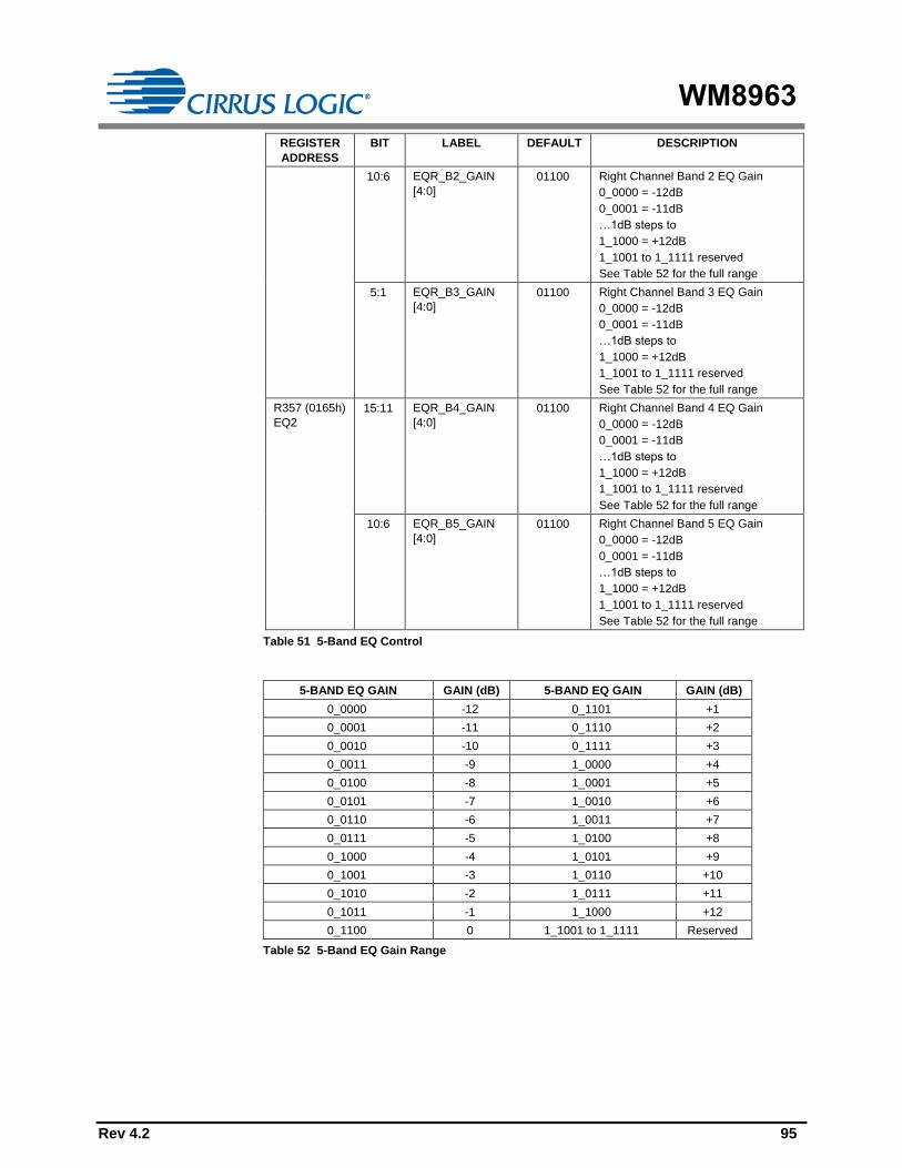
WM8963
Rev 4.2 95
REGISTER
ADDRESS
BIT LABEL DEFAULT DESCRIPTION
10:6 EQR_B2_GAIN
[4:0]
01100 Right Channel Band 2 EQ Gain
0_0000 = -12dB
0_0001 = -11dB
…1dB steps to
1_1000 = +12dB
1_1001 to 1_1111 reserved
See Table 52 for the full range
5:1 EQR_B3_GAIN
[4:0]
01100 Right Channel Band 3 EQ Gain
0_0000 = -12dB
0_0001 = -11dB
…1dB steps to
1_1000 = +12dB
1_1001 to 1_1111 reserved
See Table 52 for the full range
R357 (0165h)
EQ2
15:11 EQR_B4_GAIN
[4:0]
01100 Right Channel Band 4 EQ Gain
0_0000 = -12dB
0_0001 = -11dB
…1dB steps to
1_1000 = +12dB
1_1001 to 1_1111 reserved
See Table 52 for the full range
10:6 EQR_B5_GAIN
[4:0]
01100 Right Channel Band 5 EQ Gain
0_0000 = -12dB
0_0001 = -11dB
…1dB steps to
1_1000 = +12dB
1_1001 to 1_1111 reserved
See Table 52 for the full range
Table 51 5-Band EQ Control
5-BAND EQ GAIN GAIN (dB) 5-BAND EQ GAIN GAIN (dB)
0_0000 -12 0_1101 +1
0_0001 -11 0_1110 +2
0_0010 -10 0_1111 +3
0_0011 -9 1_0000 +4
0_0100 -8 1_0001 +5
0_0101 -7 1_0010 +6
0_0110 -6 1_0011 +7
0_0111 -5 1_0100 +8
0_1000 -4 1_0101 +9
0_1001 -3 1_0110 +10
0_1010 -2 1_0111 +11
0_1011 -1 1_1000 +12
0_1100 0 1_1001 to 1_1111 Reserved
Table 52 5-Band EQ Gain Range

WM8963
96 Rev 4.2
DYNAMIC RANGE CONTROL (DRC)
VSSDRC
DAC Signal Enhancement path
Second Order
HPF5-band EQ MBC
DAC
ReTune™
The dynamic range controller (DRC) is a circuit which can be enabled in either the digital record
(ADC) or the digital playback (DAC) path of the WM8963. Note that the DRC cannot be enabled in
both signal paths at the same time.
The function of the DRC is to adjust the signal gain in conditions where the input amplitude is
unknown or varies over a wide range, e.g. when recording from microphones built into a handheld
system.
The DRC can apply Compression and Automatic Level Control to the signal path. It incorporates
‘anti-clip’ and ‘quick release’ features for handling transients in order to improve intelligibility in the
presence of loud impulsive noises.
The DRC also incorporates a Noise Gate function, which provides additional attenuation of very low-
level input signals. This means that the signal path is quiet when no signal is present, giving an
improvement in background noise level under these conditions.
The DRC is enabled using DRC_ENA, as described in Table 53. The DRC is selected in the DAC
signal path by setting DRC_MODE = 1.
Additional registers for configuring the DRC are described in the “ADC Signal Path Enhancements”
section.
REGISTER
ADDRESS
BIT LABEL DEFAULT DESCRIPTION
R276 (0114h)
DRC 1
1 DRC_MODE 0 DRC path select
0 = ADC path
1 = DAC path
0 DRC_ENA 0 DRC Enable
0 = Disabled
1 = Enabled
Table 53 DRC Mode and Enable

WM8963
Rev 4.2 97
DAC SECOND ORDER HIGH-PASS FILTER
VSSDRC
DAC Signal Enhancement path
Second Order
HPF5-band EQ MBC
DAC
ReTune™
The 2nd order High-Pass Filter (HPF) is part of the DAC Signal Enhancement path.
The DAC High-Pass filter is provided to remove DC offsets and low frequencies from the DAC signal
path. This is an important function as DC offsets in the audio signal will reduce the signal headroom
and increase power consumption. DC offsets and low frequency signals that are outside the
capabilities of the loudspeaker will result in audible distortion and can cause damage to speakers or
headphones.
The cut-off frequency of the DAC High-Pass filter should be set to attenuate the frequencies that the
speaker cannot reproduce, but without unnecessarily removing higher frequencies that can be
supported. The 2nd order cut-off slope of 12dB per octave provides good selectivity between the
frequencies to be cut and the frequencies to be retained.
The DAC High-Pass filter is particularly recommended for use with the VSS, DAC ReTune, and MBC
functions in order to prevent distortion and speaker damage.
Before the DAC High-Pass filter is enabled, it must be initialised and configured using the DSP2_ENA
bit described in Table 54. Note that this bit only needs to be enabled once before using any or all of
DAC ReTune, DAC HPF, VSS or MBC.
Note that specific sequences must be followed when enabling or configuring DAC ReTune, DAC HPF,
VSS and MBC functions (see “DSP Signal Enhancements”).
The 2nd order High Pass Filter comprises two 1st order filters, which are enabled using the HPF1_ENA
and HPF2_ENA register bits as described in Table 54. Either one of the filters, or both filters, may be
enabled. Each filter provides a cut-off slope of 6dB per octave; when both filters are enabled together,
the combined effect is a second-order filter, with a cut-off slope of 12dB per octave.
Note that the DAC high pass filters cannot be enabled unless one or more other sound enhancement
functions is enabled. If HPF1_ENA = 1 or HPF2_ENA = 1, then at least one other of the enable bits in
Register R16389 must also be set (ie. RTN_DAC_ENA, VSS_ENA or MBC_ENA).
For the derivation of the High-Pass Filter configuration parameters in registers R17408 and R17409,
refer to the WISCETM configuration tool supplied with the WM8963 Evaluation Kit. Note that both filters
(HPF1 and HPF2) use the same configuration parameters.
REGISTER
ADDRESS
BIT LABEL DEFAULT DESCRIPTION
R768 (R300h)
DSP2 Power
Management
0 DSP2_ENA 0 DSP2 Audio Processor Enable.
0 = Disabled
1 = Enabled
This bit must be set before any of
DAC ReTune, DAC HPF, VSS or
MBC is enabled. It must remain set
whenever any of these functions is
enabled.
R16389 (4005h)
SOUNDSTAGE
_ENABLES_0
2 HPF2_ENA 0 High-Pass Filter (HPF2) enable
0 = Disabled
1 = Enabled
1 HPF1_ENA 0 High Pass Filter (HPF1) enable
0 = Disabled
1 = Enabled
Table 54 DAC High Pass Filter Enable

WM8963
98 Rev 4.2
VIRTUAL SURROUND SOUND (VSS)
VSSDRC
DAC Signal Enhancement path
Second Order
HPF5-band EQ MBC
DAC
ReTune™
The Virtual Surround Sound (VSS) function is part of the DAC Signal Enhancement path.
Virtual Sound Sound (VSS) is a digital processing function that creates a perception of wider speaker
separation, generating a rich and immersive listening experience. It is aimed at portable applications,
but is effective on larger systems also. Note that VSS is not suited to single-speaker systems, nor to
headphone outputs.
Portable applications, where the speaker separation is small, suffer from significant acoustic crosstalk,
where the Right speaker output is heard strongly in the Left ear, and vice versa. The VSS algorithms
are designed to minimise these crosstalk effects, thus increasing the stereo experience. The VSS
process is finely tuned to produce a compelling three-dimensional experience, but without the listening
fatigue associated with some other stereo enhancement systems.
The VSS algorithms (and the user perception) are most effective at high frequencies; low frequency
content is therefore configured to bypass the VSS crosstalk processing. The crossover frequency (for
the low-frequency bypass) is adjustable, enabling the user to trade-off the stereo widening effect
against the required degree of integrity in the original audio.
The VSS algorithms are programmable and can be optimised for specific application or user
geometries. It is recommended to use the DAC HPF in conjunction with VSS in order to prevent
distortion and speaker damage.
Before VSS is enabled, it must be initialised and configured using the DSP2_ENA bit described in
Table 55. Note that this bit only needs to be enabled once before using any or all of DAC ReTune,
DAC HPF, VSS or MBC.
Note that specific sequences must be followed when enabling or configuring DAC ReTune, DAC HPF,
VSS and MBC functions (see “DSP Signal Enhancements”).
VSS is enabled using the VSS_ENA register bit as described in Table 55.
It is possible to configure the VSS function to create a stereo effect that is optimised and tailored
specifically for a particular application. For the derivation of the VSS configuration parameters in
registers R19456 to R19603, refer to the WISCETM configuration tool supplied with the WM8963
Evaluation Kit. Note that DSP2_ENA must be enabled before there is any type of access of any of the
parameters associated with VSS.
REGISTER
ADDRESS
BIT LABEL DEFAULT DESCRIPTION
R768 (R300h)
DSP2 Power
Management
0 DSP2_ENA 0 DSP2 Audio Processor Enable.
0 = Disabled
1 = Enabled
This bit must be set before any of
DAC ReTune, DAC HPF, VSS or
MBC is enabled. It must remain set
whenever any of these functions is
enabled.
R16389
(4005h)
SOUNDSTAG
E_ENABLES_
0
0 VSS_ENA 0 Virtual Surround Sound (VSS)
enable
0 = Disabled
1 = Enabled
Table 55 Virtual Surround Sound (VSS) Enable

WM8963
Rev 4.2 99
DAC RETUNE
VSSDRC
DAC Signal Enhancement path
Second Order
HPF5-band EQ MBC
DAC
ReTune™
The ReTune function is part of the DAC Signal Enhancement paths. Unique coefficient sets are
supported.
ReTuneTM is an advanced feature that is intended to perform frequency linearisation according to the
particular needs of the application microphone, loudspeaker or housing. The ReTune algorithms can
provide acoustic equalisation and selective phase (delay) control of specific frequency bands. In a
typical application, ReTune™ is used to flatten the response across the audio frequency band.
ReTune™ can also be configured to achieve other response patterns if required.
It is particularly recommended to use ReTune™ to flatten the DAC signal path response when using
the VSS or MBC functions. The signal processing algorithms of the VSS and MBC functions assume a
flat system response, and the performance of these enhancements will be compromised if the
speaker response is poor or uncalibrated.
Note that, when using ReTune™ to boost any frequency band, it is recommended to take care not to
introduce distortion, taking into account the gain that may be applied by other audio enhancement
functions.
It is recommended to use the DAC HPF in conjunction with DAC ReTune in order to prevent distortion
and speaker damage.
Before ReTuneTM is enabled, it must be initialised and configured using the DSP2_ENA bit described
in Table 56. Note that this bit only needs to be enabled once before using any or all of DAC ReTune,
DAC HPF, VSS or MBC.
Note that specific sequences must be followed when enabling or configuring DAC ReTune, DAC HPF,
VSS and MBC functions (see “DSP Signal Enhancements”).
The ReTune function is enabled on the DAC path using the RTN_DAC_ENA register bit as described
in Table 56. Under default conditions, the Left and Right channels each use unique tuning coefficients.
When the DAC_RETUNE_SCV register is set, then both channels are controlled by the Right channel
coefficients.
For the derivation of DAC ReTune configuration parameters in registers R17920 to R19007, the Cirrus
Logic WISCE™ software must be used to analyse the requirements of the application (refer to
WISCETM for further information.) If desired, one or more sets of register coefficients might be derived
for different operating scenarios, and these may be recalled and written to the CODEC registers as
required in the target application. The DAC ReTune configuration procedure involves the generation
and analysis of test signals as outlined below. Note that DSP2_ENA must be enabled before there is
any type of access of any of the parameters associated with DAC ReTune.
To determine the characteristics of the loudspeaker in an application, a test signal is applied to the
target application. A reference microphone is positioned in the normal acoustic path of the
loudspeaker, and the received signal is analysed to determine how accurately the loudspeaker has
reproduced the test signal.
Note that the ReTune configuration coefficients are specific to a particular speaker or microphone; it is
therefore required that the part-to-part variation in these components is small.

WM8963
100 Rev 4.2
DAC ReTune is controlled using the register bits as described in Table 56.
REGISTER
ADDRESS
BIT LABEL DEFAULT DESCRIPTION
R768 (R300h)
DSP2 Power
Management
0 DSP2_ENA 0 DSP2 Audio Processor Enable.
0 = Disabled
1 = Enabled
This bit must be set before any of
DAC ReTune, DAC HPF, VSS or
MBC is enabled. It must remain set
whenever any of these functions is
enabled.
R16386
(4002h)
RETUNEDAC
_SHARED_C
OEFF_1
7 DAC_RETUNE_
SCV
0 DAC ReTune Coefficient sharing
0 = Left and Right channels each
use unique coefficients
1 = Both channels use the Right
Channel coefficients
R16389
(4005h)
SOUNDSTAG
E_ENABLES_
0
4 RTN_DAC_ENA 0 DAC ReTune enable
0 = disabled
1 = enabled
Table 56 DAC ReTune Enable
MULTIBAND COMPRESSOR (MBC)
VSSDRC
DAC Signal Enhancement path
Second Order
HPF5-band EQ MBC
DAC
ReTune™
The Multiband Compressor (MBC) function is part of the DAC Signal Enhancement path.
The MBC uses selective processing of the audio signal to control the loudness; independent gain
control algorithms are applied to different audio frequency bands. The effect of this is to increase the
perceived loudness of the audio path, producing an enhanced audio signal without overdriving the
output transducers (eg. loudspeakers).
The most significant advantage of multiband compression is that a signal peak in one frequency band
will not cause gain reduction in another frequency band. Similarly, gain can be applied to one
frequency band without boosting (and potentially distorting) another. This provides a powerful
capability to maximise the loudness of the signal path.
It is recommended to use the DAC HPF in conjunction with the MBC in order to prevent distortion and
speaker damage.
Before the MBC is enabled, it must be initialised and configured using the DSP2_ENA bit described in
Table 57. Note that this bit only needs to be enabled once before using any or all of DAC ReTune,
DAC HPF, VSS or MBC.
Note that specific sequences must be followed when enabling or configuring DAC ReTune, DAC HPF,
VSS and MBC functions (see “DSP Signal Enhancements”).
MBC is enabled using the MBC_ENA register bit as described in Table 57.
The MBC is pre-configured with a default set of parameters, but alternative settings can also be
configured. The multiband crossover frequencies, and gain/compression parameters are all
adjustable.
For the derivation of the MBC configuration parameters in registers R16896 to R16955, refer to the
WISCETM configuration tool supplied with the WM8963 Evaluation Kit. Note that DSP2_ENA must be
enabled before there is any type of access of any of the parameters associated with MBC.

WM8963
Rev 4.2 101
REGISTER
ADDRESS
BIT LABEL DEFAULT DESCRIPTION
R768 (R300h)
DSP2 Power
Management
0 DSP2_ENA 0 DSP2 Audio Processor Enable.
0 = Disabled
1 = Enabled
This bit must be set before any of
DAC ReTune, DAC HPF, VSS or
MBC is enabled. It must remain set
whenever any of these functions is
enabled.
R16389 (4005h)
SOUNDSTAGE
_ENABLES_0
3 MBC_ENA 0 MBC Enable
0 = Disabled
1 = Enabled
Table 57 Multiband Compressor Control
DIGITAL-TO-ANALOGUE CONVERTER (DAC)
The WM8963 DACs receive digital input data from the digital audio interface. The digital audio data is
converted to oversampled bit-streams in the on-chip, true 24-bit digital interpolation filters. The bit-
stream data enters two multi-bit, sigma-delta DACs, which convert them to high quality analogue
audio signals.
The DACs provide digital volume control with soft mute / un-mute. Digital mono mix and de-emphasis
filtering is also supported.
The DACs are enabled by the DACL_ENA and DACR_ENA register bits.
The system clock, SYSCLK, must be configured and enabled before either of the DACs is enabled.
See “Clocking and Sample Rates” for details of the system clocks.
Note that, when reconfiguring or disabling SYSCLK, the ADCs and DACs must be disabled before
setting SYSCLK_ENA=0.
REGISTER
ADDRESS
BIT LABEL DEFAULT DESCRIPTION
R26 (1Ah)
Pwr Mgmt (2)
8 DACL_ENA 0 Left DAC Enable
0 = Disabled
1 = Enabled
Note that DACL_ENA must be set
to 1 when processing left channel
data from the DAC or Digital Beep
Generator.
7 DACR_ENA 0 Right DAC Enable
0 = Disabled
1 = Enabled
Note that DACR_ENA must be set
to 1 when processing right channel
data from the DAC or Digital Beep
Generator.
Table 58 DAC Enable Control
DAC CLOCKING CONTROL
Clocking for the DACs is derived from SYSCLK. The required clock is enabled when the
SYSCLK_ENA register is set.
The DAC clock rate is configured automatically, according to the SAMPLE_RATE and MCLK_RATE
registers. See “Clocking and Sample Rates” for further details of the system clocks and associated
control registers.
Note that the DAC and the DAC signal path enhancements functions are only supported under
specific clocking configurations. The valid clocking ratios for DAC operation are identified in Table 92.
See also Table 93 for details of the supported functions for different MCLK / fs ratios.

WM8963
102 Rev 4.2
DAC DIGITAL VOLUME CONTROL
The output level (digital volume) of each DAC can be controlled digitally over a range from -71.625dB
to +23.625dB in 0.375dB steps. The level of attenuation for an eight-bit code X is given by:
0.375 (X-192) dB for 1 X 255; MUTE for X = 0
The DAC_VU bit controls the loading of digital volume control data. When DAC_VU is set to 0, the
DACL_VOL or DACR_VOL control data will be loaded into the respective control register, but will not
actually change the digital gain setting. Both left and right gain settings are updated when a 1 is
written to DAC_VU. This makes it possible to update the gain of both channels simultaneously.
See "DAC Digital Volume Control" section for a description of the volume update function, the zero
cross function and the timeout operation.
REGISTER
ADDRESS
BIT LABEL DEFAULT DESCRIPTION
R10 (0Ah)
Left DAC
volume
8 DAC_VU N/A DAC Volume Update
Writing a 1 to this bit will cause left
and right DAC volume to be updated
simultaneously
7:0 DACL_VOL
[7:0]
C0h
(0dB)
Left DAC Digital Volume Control
00h = Digital Mute
01h = -71.625dB
02h = -71.250dB
... 0.375dB steps up to
C0h = 0dB (default)
….
FFh = 23.625dB
(See Table 60 for volume range)
R11 (0Bh)
Right DAC
volume
8 DAC_VU N/A DAC Volume Update
Writing a 1 to this bit will cause left
and right DAC volume to be updated
simultaneously
7:0 DACR_VOL
[7:0]
C0h
(0dB)
Right DAC Digital Volume Control
00h = Digital Mute
01h = -71.625dB
02h = -71.250dB
... 0.375dB steps up to
C0h = 0dB (default)
….
FFh = 23.625dB
(See Table 60 for volume range)
Table 59 Digital Volume Control

WM8963
Rev 4.2 103
DACL_VOL or
DACR_VOL Volume (dB)
DACL_VOL or
DACR_VOL Volume (dB)
DACL_VOL or
DACR_VOL Volume (dB)
DACL_VOL or
DACR_VOL Volume (dB)
00 MUTE 40 -48.000 80 -24.000 C0 0.000
01 -71.625 41 -47.625 81 -23.625 C1 0.375
02 -71.250 42 -47.250 82 -23.250 C2 0.750
03 -70.875 43 -46.875 83 -22.875 C3 1.125
04 -70.500 44 -46.500 84 -22.500 C4 1.500
05 -70.125 45 -46.125 85 -22.125 C5 1.875
06 -69.750 46 -45.750 86 -21.750 C6 2.250
07 -69.375 47 -45.375 87 -21.375 C7 2.625
08 -69.000 48 -45.000 88 -21.000 C8 3.000
09 -68.625 49 -44.625 89 -20.625 C9 3.375
0A -68.250 4A -44.250 8A -20.250 CA 3.750
0B -67.875 4B -43.875 8B -19.875 CB 4.125
0C -67.500 4C -43.500 8C -19.500 CC 4.500
0D -67.125 4D -43.125 8D -19.125 CD 4.875
0E -66.750 4E -42.750 8E -18.750 CE 5.250
0F -66.375 4F -42.375 8F -18.375 CF 5.625
10 -66.000 50 -42.000 90 -18.000 D0 6.000
11 -65.625 51 -41.625 91 -17.625 D1 6.375
12 -65.250 52 -41.250 92 -17.250 D2 6.750
13 -64.875 53 -40.875 93 -16.875 D3 7.125
14 -64.500 54 -40.500 94 -16.500 D4 7.500
15 -64.125 55 -40.125 95 -16.125 D5 7.875
16 -63.750 56 -39.750 96 -15.750 D6 8.250
17 -63.375 57 -39.375 97 -15.375 D7 8.625
18 -63.000 58 -39.000 98 -15.000 D8 9.000
19 -62.625 59 -38.625 99 -14.625 D9 9.375
1A -62.250 5A -38.250 9A -14.250 DA 9.750
1B -61.875 5B -37.875 9B -13.875 DB 10.125
1C -61.500 5C -37.500 9C -13.500 DC 10.500
1D -61.125 5D -37.125 9D -13.125 DD 10.875
1E -60.750 5E -36.750 9E -12.750 DE 11.250
1F -60.375 5F -36.375 9F -12.375 DF 11.625
20 -60.000 60 -36.000 A0 -12.000 E0 12.000
21 -59.625 61 -35.625 A1 -11.625 E1 12.375
22 -59.250 62 -35.250 A2 -11.250 E2 12.750
23 -58.875 63 -34.875 A3 -10.875 E3 13.125
24 -58.500 64 -34.500 A4 -10.500 E4 13.500
25 -58.125 65 -34.125 A5 -10.125 E5 13.875
26 -57.750 66 -33.750 A6 -9.750 E6 14.250
27 -57.375 67 -33.375 A7 -9.375 E7 14.625
28 -57.000 68 -33.000 A8 -9.000 E8 15.000
29 -56.625 69 -32.625 A9 -8.625 E9 15.375
2A -56.250 6A -32.250 AA -8.250 EA 15.750
2B -55.875 6B -31.875 AB -7.875 EB 16.125
2C -55.500 6C -31.500 AC -7.500 EC 16.500
2D -55.125 6D -31.125 AD -7.125 ED 16.875
2E -54.750 6E -30.750 AE -6.750 EE 17.250
2F -54.375 6F -30.375 AF -6.375 EF 17.625
30 -54.000 70 -30.000 B0 -6.000 F0 18.000
31 -53.625 71 -29.625 B1 -5.625 F1 18.375
32 -53.250 72 -29.250 B2 -5.250 F2 18.750
33 -52.875 73 -28.875 B3 -4.875 F3 19.125
34 -52.500 74 -28.500 B4 -4.500 F4 19.500
35 -52.125 75 -28.125 B5 -4.125 F5 19.875
36 -51.750 76 -27.750 B6 -3.750 F6 20.250
37 -51.375 77 -27.375 B7 -3.375 F7 20.625
38 -51.000 78 -27.000 B8 -3.000 F8 21.000
39 -50.625 79 -26.625 B9 -2.625 F9 21.375
3A -50.250 7A -26.250 BA -2.250 FA 21.750
3B -49.875 7B -25.875 BB -1.875 FB 22.125
3C -49.500 7C -25.500 BC -1.500 FC 22.500
3D -49.125 7D -25.125 BD -1.125 FD 22.875
3E -48.750 7E -24.750 BE -0.750 FE 23.250
3F -48.375 7F -24.375 BF -0.375 FF 23.625
Table 60 DAC Digital Volume Range

WM8963
104 Rev 4.2
DAC SOFT MUTE AND UN-MUTE
The WM8963 has both hard and soft mute functions. If DAC_MUTE_RAMP=0, any muting of the
output volume is instantaneous.
The WM8963 also has a soft mute function which, when enabled (DAC_MUTE_RAMP=1), gradually
attenuates the volume of the digital signal to zero. When soft mute is disabled, the gain will either
gradually ramp back up to the digital gain setting, or return instantly to the digital gain setting,
depending on the DAC_UNMUTE_RAMP register bit.
The DAC is soft-muted by default. To play back an audio signal, this function must first be disabled by
setting the DAC_MUTE bit to zero.
DAC_UNMUTE_RAMP would typically be enabled when using soft mute during playback of audio
data so that when soft mute is then disabled, the sudden volume increase will not create pop noise by
jumping immediately to the previous volume level (e.g. resuming playback after pausing during a
track).
DAC_UNMUTE_RAMP would typically be disabled when un-muting at the start of a digital music file,
so that the first part of the track is not attenuated (e.g. when starting playback of a new track, or
resuming playback after pausing between tracks).
DAC_MUTE_RAMP = 0 and DAC_UNMUTE_RAMP = 0
DAC muting and un-muting with soft mute and soft unmute
disabled
(DAC_MUTE_RAMP = 0 and DAC_UNMUTE_RAMP = 0)
DAC muting and un-muting with soft mute and soft unmute
enabled
(DAC_MUTE_RAMP = 1 and DAC_UNMUTE_RAMP = 1)
DAC_MUTE = 0 DAC_MUTE = 1 DAC_MUTE = 0
DAC_MUTE_RAMP = 1 and DAC_UNMUTE_RAMP = 1
DAC_MUTE = 0 DAC_MUTE = 1 DAC_MUTE = 0
Figure 32 DAC Mute Control

WM8963
Rev 4.2 105
The volume ramp rate during soft mute and un-mute is controlled by the DAC_MUTERATE bit as
shown in Table 61.
REGISTER
ADDRESS
BIT LABEL DEFAULT DESCRIPTION
R5 (05h)
ADC and DAC
Control 1
4 DAC_MUTE_RAMP 1 DAC Soft Mute Control
0 = Muting the DAC
(DAC_MUTE = 1) will cause the
volume to change immediately to
mute.
1 = Muting the DAC
(DAC_MUTE = 1) will cause the
volume to ramp down gradually
to mute.
3 DAC_MUTE 1 Digital DAC Mute
0 = Un-mute
1 = Mute
Note that this bit also exists in
R49. Reading or writing to either
location has the same effect.
R49 (31h)
Class D
Control (1)
4 DAC_MUTE 1 Digital DAC Mute
0 = Un-mute
1 = Mute
Note that this bit also exists in
R5. Reading or writing to either
location has the same effect.
R6 (06h)
ADC and DAC
Control 2
3 DAC_UNMUTE_RAMP 1 DAC Soft Unmute Control
0 = Unmuting the DAC
(DAC_MUTE = 0) will cause the
volume to change immediately to
the DACL_VOL/DACR_VOL
settings.
1 = Unmuting the DAC
(DAC_MUTE = 0) will cause the
volume to ramp up gradually to
the DACL_VOL/DACR_VOL
settings.
2 DAC_MUTERATE 0 DAC Soft Mute Ramp Rate
0 = Fast ramp (maximum ramp
time 10.7ms)
1 = Slow ramp (maximum ramp
time 171ms).
Note that the ramp rate scales
with sample rate (fs). Quoted
values are correct for fs =
48kHz.
Table 61 DAC Soft-Mute Control

WM8963
106 Rev 4.2
DAC AUTO-MUTE
The DAC digital mute and volume controls are described earlier in Table 59 and Table 61.
The DAC also incorporates a digital auto-mute monitor, which is enabled by setting
DAC_AUTOMUTE. When the auto-mute is enabled, and a number (DAC_AUTOMUTE_SAMPLES) of
consecutive zero-samples is detected, the AUTOMUTE_STS flag is asserted.
The WM8963 supports the option to automatically power-down the speaker path when the DAC Auto-
Mute is triggered, and to re-enable the speaker path when audio data is detected. This feature has
been designed to work around the Write Sequencer, which mutes and unmutes the speakers in a
controlled manner using the Speaker Sleep (see Table 123) and Speaker Wake (see Table 124) write
sequences. Auto-mute is enabled by setting the WSEQ_AUTOSEQ_ENA bit in Register R87. See
Table 62 for details of this and other Auto-mute register bits.
The status of DAC Auto-Mute can be read back from the AUTOMUTE_STS bit.
REGISTER
ADDRESS
BIT LABEL DEFAULT DESCRIPTION
R9 (09h)
Audio
Interface 0
11 AUTOMUTE_STS 0 Readback of the DAC automute
status
0 = Automute not detected
1 = Automute detected
9:8 DAC_AUTOMUT
E_SAMPLES [1:0]
11 Selects the number of consecutive
zero DAC samples that will be
interpreted as an Automute.
00 = 128 samples
01 = 256 samples
10 = 512 samples
11 = 1024 samples
7 DAC_AUTOMUT
E
0 DAC Auto-Mute Control
0 = Disabled
1 = Enabled
R87 (57h)
Write
Sequencer
Control 1
7 WSEQ_AUTOSE
Q_ENA
0 Write Sequencer Auto-Sequence
Enable (controls the Class D driver
via DAC Auto-Mute function)
0 = Disabled
1 = Enabled
Table 62 DAC Auto Mute
DAC MONO MIX
A DAC digital mono-mix mode can be enabled using the DAC_MONOMIX register bit. This mono mix
will be output on whichever DAC is enabled. To prevent clipping, a -6dB attenuation is automatically
applied to the mono mix.
The mono mix is only supported when one or other DAC is disabled. When the mono mix is selected,
then the mono mix is output on the enabled DAC only; there is no output from the disabled DAC. If
DACL_ENA and DACR_ENA are both set, then stereo operation applies.
REGISTER
ADDRESS
BIT LABEL DEFAULT DESCRIPTION
R57(39h)
DAC DSP Mixing
(1)
9 DAC_MONOMIX 0 DAC Mono Mix
0 = Stereo
1 = Mono (Mono mix output on
enabled DAC)
Mono Mix is only supported
when one or other DAC is
disabled.
When Mono mix is enabled,
6dB attenuation is applied.
Table 63 DAC Mono Mix

WM8963
Rev 4.2 107
DAC DE-EMPHASIS
Digital de-emphasis can be applied to the DAC playback data (e.g. when the data comes from a CD
with pre-emphasis used in the recording). De-emphasis filtering is available for sample rates of 48kHz,
44.1kHz and 32kHz.
REGISTER
ADDRESS
BIT LABEL DEFAULT DESCRIPTION
R5 (05h)
ADC and DAC
Control 1
2:1 DAC_DEEMP
[1:0]
00 De-Emphasis Control
00 = No de-emphasis
01 = De-emphasis for 32kHz sample
rate
10 = De-emphasis for 44.1kHz
sample rate
11 = De-emphasis for 48kHz sample
rate
Table 64 DAC De-Emphasis Control
DAC OVERSAMPLING RATIO (OSR)
The DAC oversampling rate is programmable to allow power consumption versus audio performance
trade-offs. The default oversampling rate is low for reduced power consumption; using the higher OSR
setting improves the DAC signal-to-noise performance.
See the “Reference Voltages and Bias Control” section for details of the supported bias control
settings for the output signal paths.
REGISTER
ADDRESS
BIT LABEL DEFAULT DESCRIPTION
R6 (06h)
ADC and DAC
Control 2
0 DAC_HP 0 DAC Oversampling Ratio
0 = Low Power (typically 64 x fs)
1 = High Performance (typically 128 x
fs)
Table 65 DAC Oversampling Control

WM8963
108 Rev 4.2
DIGITAL BEEP GENERATOR
The WM8963 provides a digital signal generator which can be used to inject an audio tone (beep) into
the DAC signal path. The output of the beep generator is digitally mixed with the DAC outputs, after
the DAC digital volume.
The beep is enabled using BEEP_ENA. The beep function creates an approximation of a Sine wave.
The audio frequency is set using BEEP_RATE, and is dependent on the SAMPLE_RATE_INT_MODE
and the SAMPLE_RATE settings (see “Clocking and Sample Rates” section). The beep volume is set
using BEEP_GAIN. Note that the volume of the digital beep generator is not affected by the DAC
volume or DAC mute controls.
The digital beep generator control fields are described in Table 66.
REGISTER
ADDRESS
BIT LABEL DEFAULT DESCRIPTION
R110 (6Eh)
Beep
Generator (1)
7:4 BEEP_GAIN [3:0] 0000 Digital Beep Volume Control
0000 = mute
0001 = -90dB
0010 = -84dB
… (6dB steps)
1111 = -6dB
2:1 BEEP_RATE [1:0] 01 Digital Beep Waveform Control
If SAMPLE_RATE_INT_MODE = 1
00 = 500Hz
01 = 1000Hz
10 = 2000Hz
11 = 4000Hz
If SAMPLE_RATE_INT_MODE = 0
00 = 499Hz – 502Hz
01 = 999Hz – 1003Hz
10 = 1998Hz – 2005Hz
11 = 3997Hz – 4009Hz
0 BEEP_ENA 0 Digital Beep Enable
0 = Disabled
1 = Enabled
Note that the DAC and associated
signal path needs to be enabled
when using the digital beep.
Table 66 Digital Beep Generator

WM8963
Rev 4.2 109
OUTPUT SIGNAL PATH
The WM8963 provides two stereo Headphone Output drivers and a pair of Speaker Output drivers.
The speaker output mixers, and associated multiplexers, provide a high degree of flexibility, allowing
multiple signal paths through the device to the outputs.
The output signal paths and associated control registers are illustrated in Figure 33.
IN4
R
IN4
L
MIX
INL
MIX
INR
DACL
DACR
IN4L
MIXINL
MIXINR
IN4R
DACL
DACR
IN4L
MIXINL
MIXINR
IN4R
SP
KM
IXL
SP
KM
IXL
_E
NA
/ S
PK
MIX
L_
MU
TE
SP
KM
IXR
SP
KM
IXR
_E
NA
/ S
PK
MIX
R_
MU
TE
SP
KM
IXL
_T
O_
HP
OU
TL
_P
GA
DA
CL
_T
O_
SP
KM
IXR
/ D
AC
L_
SP
KM
IXR
_V
OL
DA
CR
_T
O_
SP
KM
IXR
/ D
AC
R_
SP
KM
IXR
_V
OL
MIX
INL_
TO
_S
PK
MIX
R / M
IXIN
L_
SP
KM
IXR
_V
OL
MIX
INR
_T
O_
SP
KM
IXR
/ M
IXIN
R_
SP
KM
IXR
_V
OL
IN4
L_T
O_
SP
KM
IXR
/ I
N4
L_
SP
KM
IXR
_V
OL
IN4
R_
TO
_S
PK
MIX
R / I
N4
R_
SP
KM
IXR
_V
OL
DA
CL
_T
O_
SP
KM
IXL
/ D
AC
L_
SP
KM
IXL
_V
OL
DA
CR
_T
O_
SP
KM
IXL
/ D
AC
R_
SP
KM
IXL
_V
OL
MIX
INL_
TO
_S
PK
MIX
L / M
IXIN
L_
SP
KM
IXL
_V
OL
MIX
INR
_T
O_
SP
KM
IXL
/ M
IXIN
R_
SP
KM
IXL
_V
OL
IN4
L_
TO
_S
PK
MIX
L /
IN
4L
_S
PK
MIX
L_
VO
L
IN4
R_
TO
_S
PK
MIX
L / IN
4R
_S
PK
MIX
L_
VO
L
SP
KM
IXR
_T
O_
HP
OU
TR
_P
GA
SP
KM
IXL
_T
O_
SP
KO
UT
L_
PG
A
1 0
SP
KM
IXR
_T
O_
SP
KO
UT
R_
PG
A
MIX
ER
PG
A K
EY
=
-1
5d
B to
+6
dB
=
0d
B o
r -6
dB
*
1 0 0 1 0 1
+
* * **
+
****
HP
OU
T1L
HP
OU
T1R
SP
KO
UT
LP
SP
KO
UT
LN
SP
KO
UT
RP
SP
KO
UT
RN
HP
OU
TF
B
HP
OU
T2L
HP
OU
T2R
HP
OU
TL
HP
OU
TR
SP
KO
UT
L
SP
KO
UT
R
HP
2L
HP
1L
HP
1R
HP
2R
SP
KR
SP
KL
HP
OU
TL
_P
GA
_E
NA
HP
OU
TR
_P
GA
_E
NA
SP
KO
UT
L_
PG
A_
EN
A
SP
KO
UT
R_
PG
A_
EN
A
SP
KO
UT
L_
EN
A
SP
KO
UT
R_
EN
A
HP
1L
_V
OL
HP
1R
_V
OL
HP
2L
_V
OL
HP
2R
_V
OL
HP
2L
_E
NA
HP
2R
_E
NA
HP
1R
_E
NA
HP
1L
_E
NA
CL
AS
SD
_V
OL
CL
AS
SD
_V
OL
HP
OU
TL
_V
OL
HP
OU
TL
_Z
C
HP
OU
T_
VU
HP
OU
TL
_P
GA
_M
UT
E
HP
OU
TR
_V
OL
HP
OU
TR
_Z
C
HP
OU
T_
VU
HP
OU
TR
_P
GA
_M
UT
E
SP
KO
UT
R_
VO
L
SP
KO
UT
R_
ZC
SP
KO
UT
_V
U
HP
OU
TR
_V
OL
HP
OU
TR
_Z
C
HP
OU
T_
VU
HP
OU
TR
_P
GA
_M
UT
E
HP
2_
PG
A_
SE
L =
0H
P2
_P
GA
_S
EL
= 1
SP
KO
UT
R_
PG
A_
MU
TE
SP
KO
UT
L_
VO
L
SP
KO
UT
L_
ZC
SP
KO
UT
_V
U
SP
KO
UT
L_
PG
A_
MU
TE
HP
OU
TL
_V
OL
HP
OU
TL
_Z
C
HP
OU
T_
VU
HP
OU
TL
_P
GA
_M
UT
E
HP
2_
PG
A_
SE
L =
0H
P2
_P
GA
_S
EL
= 1
DA
CL
_E
NA
DA
CR
_E
NA
DA
C
SIG
NA
L
PR
OC
ES
SIN
G
DA
CL
_V
OL
DA
C_
MU
TE
DA
C_
MU
TE
_R
AM
P
DA
C_
UN
MU
TE
_R
AM
P
DA
C_
MU
TE
RA
TE
DA
CR
_V
OL
DA
C_
MU
TE
DA
C_
MU
TE
_R
AM
P
DA
C_
UN
MU
TE
_R
AM
P
DA
C_
MU
TE
RA
TE
DA
C
DA
C
Dig
ita
l
Be
ep
Ge
ne
rato
r
Figure 33 Output Signal Paths

WM8963
110 Rev 4.2
OUTPUT SIGNAL PATHS ENABLE
The speaker output mixers, and each analogue output pin and associated PGA can be independently
enabled or disabled using the register bits described in Table 67.
The Class D speaker driver is controlled using SPKOUTL_ENA and SPKOUTR_ENA. The headphone
drivers are controlled by HP1L_ENA and HP1R_ENA, and by HP2L_ENA and HP2R_ENA (described
in Table 70).
To enable the output PGAs, the reference voltage VMID and the bias current must also be enabled.
See “Reference Voltages and Bias Control” for details of the associated controls VMID_SEL and
BIAS_ENA.
SPKOUTL and SPKOUTR are driven by the left and right speaker PGAs respectively.
HPOUT1L and HPOUT1R are driven by the left and right headphone PGAs respectively.
The input signal to the each of the PGAs is selectable between one of the speaker output mixers and
a direct output from one of the DACs.
Note that HPOUT2L and HPOUT2R are driven by the left and right speaker PGAs, but can be
configured to use the same controls as the headphone PGAs, in order to save register writes when
configuring two headphone outputs simultaneously. This is illustrated in Figure 33.
REGISTER
ADDRESS
BIT LABEL DEFAULT DESCRIPTION
R26 (1Ah)
Pwr Mgmt (2)
6 HPOUTL_PGA_E
NA
0 Headphone Left PGA enable
0 = Disabled
1 = Enabled
Note that this must be set for
HPOUT1L output.
Note that this must also be set for
HPOUT2L output if
HP2_PGA_SEL=1.
5 HPOUTR_PGA_E
NA
0 Headphone Right PGA enable
0 = Disabled
1 = Enabled
Note that this must be set for
HPOUT1R output.
Note that this must also be set for
HPOUT2R output if
HP2_PGA_SEL=1.
4 SPKOUTL_PGA_
ENA
0 Speaker Left PGA enable
0 = Disabled
1 = Enabled
Note that this must be set for
SPKOUTL, and for HPOUT2L
output if HP2_PGA_SEL=0.
3 SPKOUTR_PGA_
ENA
0 Speaker Right PGA enable
0 = Disabled
1 = Enabled
Note that this must be set for
SPKOUTR, and for HPOUT2R
output if HP2_PGA_SEL=0.
R49 (31h)
Class D
Control (1)
7 SPKOUTR_ENA 0 Right channel class D Speaker
Enable
0 = Disabled
1 = Enabled
6 SPKOUTL_ENA 0 Left channel class D Speaker
Enable
0 = Disabled
1 = Enabled

WM8963
Rev 4.2 111
REGISTER
ADDRESS
BIT LABEL DEFAULT DESCRIPTION
R99 (63h)
Mixer Enables
1 SPKMIXL_ENA 0 Left Speaker Mixer Enable
0 = Disabled
1 = Enabled
0 SPKMIXR_ENA 0 Right Speaker Mixer Enable
0 = Disabled
1 = Enabled
Table 67 Output Signal Paths Enable
HEADPHONE SIGNAL PATHS ENABLE
The Headphone output paths can be actively switched to AGND through internal resistors if desired.
This is desirable at start-up in order to achieve a known condition prior to enabling the output. This is
also desirable in shutdown to prevent the external connections from being affected by the internal
circuits. The ground-referenced Headphone outputs are shorted to AGND by default; the short circuit
is removed on each of these paths by setting the applicable fields HP1L_RMV_SHORT,
HP1R_RMV_SHORT, HP2L_RMV_SHORT or HP2R_RMV_SHORT.
The ground-referenced Headphone output drivers are designed to suppress pops and clicks when
enabled or disabled. However, it is necessary to control the drivers in accordance with a defined
sequence in start-up and shut-down to achieve the pop suppression. It is also necessary to schedule
the DC Servo offset correction at the appropriate point in the sequence (see “DC Servo”). Table 68
and Table 69 describe the recommended sequences for enabling and disabling these output drivers.
SEQUENCE HPOUT1 ENABLE HPOUT2 ENABLE
Step 1 HP1L_ENA = 1
HP1R_ENA = 1
HP2L_ENA = 1
HP2R_ENA = 1
Step 2 20μs delay 20μs delay
Step 3 HP1L_ENA_DLY = 1
HP1R_ENA_DLY = 1
HP2L_ENA_DLY = 1
HP2R_ENA_DLY = 1
Step 4 DC offset correction DC offset correction
Step 5 HP1L_ENA_OUTP = 1
HP1R_ENA_OUTP = 1
HP2L_ENA_OUTP = 1
HP2R_ENA_OUTP = 1
Step 6 20μs delay 20μs delay
Step 7 HP1L_RMV_SHORT = 1
HP1R_RMV_SHORT = 1
HP2L_RMV_SHORT = 1
HP2R_RMV_SHORT = 1
Table 68 Headphone Output Enable Sequence
SEQUENCE HPOUT1 DISABLE HPOUT2 DISABLE
Step 1 HP1L_RMV_SHORT = 0
HP1R_RMV_SHORT = 0
HP2L_RMV_SHORT = 0
HP2R_RMV_SHORT = 0
Step 2 20μs delay 20μs delay
Step 3 HP1L_ENA = 0
HP1L_ENA_DLY = 0
HP1L_ENA_OUTP = 0
HP1R_ENA = 0
HP1R_ENA_DLY = 0
HP1R_ENA_OUTP = 0
HP2L_ENA = 0
HP2L_ENA_DLY = 0
HP2L_ENA_OUTP = 0
HP2R_ENA = 0
HP2R_ENA_DLY = 0
HP2R_ENA_OUTP = 0
Table 69 Headphone Output Disable Sequence

WM8963
112 Rev 4.2
The register bits relating to pop suppression control are defined in Table 70.
REGISTER
ADDRESS
BIT LABEL DEFAULT DESCRIPTION
R69 (45h)
Analogue
HP 0
7 HP1L_RMV_SHO
RT
0 Removes HP1L short
0 = HP1L short enabled
1 = HP1L short removed
For pop-free operation, this bit should
be set to 1 as the final step in the
HP1L Enable sequence.
6 HP1L_ENA_OUT
P
0 Enables HP1L output stage
0 = Disabled
1 = Enabled
For pop-free operation, this bit should
be set to 1 after the DC offset
cancellation has been performed.
5 HP1L_ENA_DLY 0 Enables HP1L intermediate stage
0 = Disabled
1 = Enabled
For pop-free operation, this bit should
be set to 1 after the output signal path
has been configured, and before the
DC Offset cancellation is scheduled
This bit should be set with at least
20us delay after HP1L_ENA.
4 HP1L_ENA 0 Enables HP1L input stage
0 = Disabled
1 = Enabled
For pop-free operation, this bit should
be set to 1 as the first stage of the
HP1L Enable sequence.
3 HP1R_RMV_SHO
RT
0 Removes HP1R short
0 = HP1R short enabled
1 = HP1R short removed
For pop-free operation, this bit should
be set to 1 as the final step in the
HP1R Enable sequence.
2 HP1R_ENA_OUT
P
0 Enables HP1R output stage
0 = Disabled
1 = Enabled
For pop-free operation, this bit should
be set to 1 after the DC offset
cancellation has been performed.
1 HP1R_ENA_DLY 0 Enables HP1R intermediate stage
0 = Disabled
1 = Enabled
For pop-free operation, this bit should
be set to 1 after the output signal path
has been configured, and before the
DC Offset cancellation is scheduled
This bit should be set with at least
20us delay after HP1R_ENA.
0 HP1R_ENA 0 Enables HP1R input stage
0 = Disabled
1 = Enabled
For pop-free operation, this bit should
be set as the first stage of the HP1R
Enable sequence.

WM8963
Rev 4.2 113
REGISTER
ADDRESS
BIT LABEL DEFAULT DESCRIPTION
R96 (60h)
Analogue
HP 3
7 HP2L_RMV_SHO
RT
0 Removes HP2L short
0 = HP2L short enabled
1 = HP2L short removed
For pop-free operation, this bit should
be set to 1 as the final step in the
HP2L Enable sequence.
6 HP2L_ENA_OUT
P
0 Enables HP2L output stage
0 = Disabled
1 = Enabled
For pop-free operation, this bit should
be set to 1 after the DC offset
cancellation has been performed.
5 HP2L_ENA_DLY 0 Enables HP2L intermediate stage
0 = Disabled
1 = Enabled
For pop-free operation, this bit should
be set to 1 after the output signal path
has been configured, and before the
DC Offset cancellation is scheduled
This bit should be set with at least
20us delay after HP2L_ENA.
4 HP2L_ENA 0 Enables HP2L input stage
0 = Disabled
1 = Enabled
For pop-free operation, this bit should
be set as the first stage of the HP2L
Enable sequence.
3 HP2R_RMV_SHO
RT
0 Removes HP2R short
0 = HP2R short enabled
1 = HP2R short removed
For pop-free operation, this bit should
be set to 1 as the final step in the
HP2R Enable sequence.
2 HP2R_ENA_OUT
P
0 Enables HP2R output stage
0 = Disabled
1 = Enabled
For pop-free operation, this bit should
be set to 1 after the DC offset
cancellation has been performed.
1 HP2R_ENA_DLY 0 Enables HP2R intermediate stage
0 = Disabled
1 = Enabled
For pop-free operation, this bit should
be set to 1 after the output signal path
has been configured, and before the
DC Offset cancellation is scheduled
This bit should be set with at least
20us delay after HP2R_ENA.
0 HP2R_ENA 0 Enables HP2R input stage
0 = Disabled
1 = Enabled
For pop-free operation, this bit should
be set as the first stage of the HP2R
Enable sequence.
Table 70 Headphone Output Signal Paths Control

WM8963
114 Rev 4.2
SPEAKER MIXER CONTROL
Two speaker output mixers, SPKMIXL and SPKMIXR, are provided on the output signal paths. Each
of these performs configurable mixing of the DAC outputs, the Input Mixer signals, and the bypass
paths directly from the IN4L/IN4R pins.
The speaker output mixers can be selected as the source for the speaker PGAs or the headphone
PGAs. Alternatively, a direct path from one of the DACs can be selected as the source of the
respective PGAs, as illustrated in Figure 34.
IN4R
IN4L
MIXINL
MIXINR
DA
CL
DA
CR
IN4
L
MIX
INL
MIX
INR
IN4
R
DA
CL
DA
CR
IN4
L
MIX
INL
MIX
INR
IN4
R
SPKMIXL
SPKMIXL_ENA / SPKMIXL_MUTE
SPKMIXR
SPKMIXR_ENA / SPKMIXR_MUTE
SPKMIXL_TO_HPOUTL_PGA
DACL_TO_SPKMIXR / DACL_SPKMIXR_VOL
DACR_TO_SPKMIXR / DACR_SPKMIXR_VOL
MIXINL_TO_SPKMIXR / MIXINL_SPKMIXR_VOL
MIXINR_TO_SPKMIXR / MIXINR_SPKMIXR_VOL
IN4L_TO_SPKMIXR / IN4L_SPKMIXR_VOL
IN4R_TO_SPKMIXR / IN4R_SPKMIXR_VOL
DACL_TO_SPKMIXL / DACL_SPKMIXL_VOL
DACR_TO_SPKMIXL / DACR_SPKMIXL_VOL
MIXINL_TO_SPKMIXL / MIXINL_SPKMIXL_VOL
MIXINR_TO_SPKMIXL / MIXINR_SPKMIXL_VOL
IN4L_TO_SPKMIXL / IN4L_SPKMIXL_VOL
IN4R_TO_SPKMIXL / IN4R_SPKMIXL_VOL
SPKMIXR_TO_HPOUTR_PGA
SPKMIXL_TO_SPKOUTL_PGA
1
0
SPKMIXR_TO_SPKOUTR_PGA
1
0
0
1
0
1
HPOUTL
HPOUTR
SPKOUTL
SPKOUTR
DAC
SIGNAL
PROCESSING
DAC
DAC
+
+
Figure 34 Speaker Output Mixer paths
Each of the inputs to the speaker output mixers is enabled independently, using the register bits
described in Table 71 and Table 72.
A selectable 0dB/-6dB volume control is provided on each of the DAC signals to the speaker output
mixer. A selectable 0dB/+6dB volume control is provided on each of the Input Mixer signals. In the
case of the IN4L and IN4R inputs, eight different levels of gain (-15dB to +6dB) can be selected.
These controls allow the signal levels to be balanced, and can also be used to help avoid signal
clipping.
The output of each mixer can be enabled or muted, using the SPKMIXL_MUTE and SPKMIXR_MUTE
bits.
The input source for each of the PGAs is selectable between one of the speaker output mixers and a
direct output from one of the DACs.
The register bits associated with the Speaker Output mixers are described in Table 71 and Table 72.

WM8963
Rev 4.2 115
REGISTER
ADDRESS
BIT LABEL DEFAULT DESCRIPTION
R100 (64h)
Headphone
Mixer (1)
7 SPKMIXL_TO_H
POUTL_PGA
0 Left Headphone PGA Path Select
0 = DACL Output
1 = SPKMIXL Output
R105 (69h)
Speaker Mixer
(1)
7 SPKMIXL_TO_SP
KOUTL_PGA
0 Left Speaker PGA Path Select
0 = DACL Output
1 = SPKMIXL Output
5 DACL_TO_SPKM
IXL
0 Left DAC to Left Speaker Mixer
select
0 = Disabled
1 = Enabled
4 DACR_TO_SPKM
IXL
0 Right DAC to Left Speaker Mixer
select
0 = Disabled
1 = Enabled
3 MIXINL_TO_SPK
MIXL
0 Left Input Mixer to Left Speaker
Mixer select
0 = Disabled
1 = Enabled
2 MIXINR_TO_SPK
MIXL
0 Right Input Mixer to Left Speaker
Mixer select
0 = Disabled
1 = Enabled
1 IN4L_TO_SPKMI
XL
0 Input IN4L to Left Speaker Mixer
select
0 = Disabled
1 = Enabled
0 IN4R_TO_SPKMI
XL
0 Input IN4R to Left Speaker Mixer
select
0 = Disabled
1 = Enabled
R107 (6Bh)
Speaker Mixer
(3)
8 SPKMIXL_MUTE 1 Left Speaker Mixer Mute
0 = Unmuted
1 = Muted
7 MIXINL_SPKMIX
L_VOL
0 Left Input Mixer to Left Speaker
Mixer volume
0 = +6dB
1 = 0dB
6 MIXINR_SPKMIX
L_VOL
0 Right Input Mixer to Left Speaker
Mixer volume
0 = +6dB
1 = 0dB
5:3 IN4L_SPKMIXL_
VOL [2:0]
111 Input IN4L to Left Speaker Mixer
Volume control
000 = -15dB
001 = -12dB
010 = -9dB
011 = -6dB
100 = -3dB
101 = 0dB
110 = +3dB
111 = +6dB

WM8963
116 Rev 4.2
REGISTER
ADDRESS
BIT LABEL DEFAULT DESCRIPTION
2:0 IN4R_SPKMIXL_
VOL [2:0]
111 Input IN4R to Left Speaker Mixer
Volume control
000 = -15dB
001 = -12dB
010 = -9dB
011 = -6dB
100 = -3dB
101 = 0dB
110 = +3dB
111 = +6dB
R109 (6Dh)
Speaker Mixer
(5)
7 DACL_SPKMIXL_
VOL
0 Left DAC to Left Speaker Mixer
volume
0 = 0dB
1 = -6dB
6 DACR_SPKMIXL
_VOL
0 Right DAC to Left Speaker Mixer
volume
0 = 0dB
1 = -6dB
Table 71 Left Speaker Mixer Control
REGISTER
ADDRESS
BIT LABEL DEFAULT DESCRIPTION
R101 (65h)
Headphone
Mixer (2)
7 SPKMIXR_TO_H
POUTR_PGA
0 Right Headphone PGA Path Select
0 = DACR Output
1 = SPKMIXR Output
R106 (6Ah)
Speaker Mixer
(2)
7 SPKMIXR_TO_S
PKOUTR_PGA
0 Right Speaker PGA Path Select
0 = DACR Output
1 = SPKMIXR Output
5 DACL_TO_SPKM
IXR
0 Left DAC to Right Speaker Mixer
select
0 = Disabled
1 = Enabled
4 DACR_TO_SPKM
IXR
0 Right DAC to Right Speaker Mixer
select
0 = Disabled
1 = Enabled
3 MIXINL_TO_SPK
MIXR
0 Left Input Mixer to Right Speaker
Mixer select
0 = Disabled
1 = Enabled
2 MIXINR_TO_SPK
MIXR
0 Right Input Mixer to Right Speaker
Mixer select
0 = Disabled
1 = Enabled
1 IN4L_TO_SPKMI
XR
0 Input IN4L to Right Speaker Mixer
select
0 = Disabled
1 = Enabled
0 IN4R_TO_SPKMI
XR
0 Input IN4R to Right Speaker Mixer
select
0 = Disabled
1 = Enabled

WM8963
Rev 4.2 117
REGISTER
ADDRESS
BIT LABEL DEFAULT DESCRIPTION
R108 (6Ch)
Speaker Mixer
(4)
8 SPKMIXR_MUTE 1 Right Speaker Mixer Mute
0 = Unmuted
1 = Muted
7 MIXINL_SPKMIX
R_VOL
0 Left Input Mixer to Right Speaker
Mixer volume
0 = +6dB
1 = 0dB
6 MIXINR_SPKMIX
R_VOL
0 Right Input Mixer to Right Speaker
Mixer volume
0 = +6dB
1 = 0dB
5:3 IN4L_SPKMIXR_
VOL [2:0]
111 Input IN4L to Right Speaker Mixer
Volume control
000 = -15dB
001 = -12dB
010 = -9dB
011 = -6dB
100 = -3dB
101 = 0dB
110 = +3dB
111 = +6dB
2:0 IN4R_SPKMIXR_
VOL [2:0]
111 Input IN4R to Right Speaker Mixer
Volume control
000 = -15dB
001 = -12dB
010 = -9dB
011 = -6dB
100 = -3dB
101 = 0dB
110 = +3dB
111 = +6dB
R109 (6Dh)
Speaker Mixer
(5)
5 DACL_SPKMIXR
_VOL
0 Left DAC to Right Speaker Mixer
volume
0 = 0dB
1 = -6dB
4 DACR_SPKMIXR
_VOL
0 Right DAC to Right Speaker Mixer
volume
0 = 0dB
1 = -6dB
Table 72 Right Speaker Mixer Control

WM8963
118 Rev 4.2
HEADPHONE OUTPUT PGA CONTROL
The input signal to the headphone output PGAs is selectable between one of the speaker output
mixers and a direct output from one of the DACs. The applicable sources are selected using the
SPKMIXL_TO_HPOUTL_PGA and SPKMIXR_TO_HPOUTR_PGA register bits for the Left and Right
channels respectively. See Table 71 and Table 72 for descriptions of these bits.
There are six headphone output PGAs – two primary (HPOUTL and HPOUTR), and four secondary
(HP1L, HP1R, HP2L, and HP2R). The headphone outputs are each controlled by a primary PGA and
a secondary PGA in series.
The HPOUT PGAs give a high degree of control from -68dB to +6dB in 1dB steps, and are common
to the HPOUT1 and HPOUT2 outputs. Dedicated secondary PGAs are provided for each of the
HPOUT1 and HPOUT2 output channels. The secondary PGAs (HP1 and HP2) provide control
from -7dB to 0dB in 1dB steps on each channel. See Figure 33 for a diagrammatic representation of
this layout.
The HPOUT PGAs are controlled using the HPOUTL_VOL and HPOUTR_VOL registers, providing
fine volume control to the HPOUT1 and HPOUT2 paths.
To prevent "zipper noise", a zero-cross function is provided on the HPOUTL and HPOUTR output
PGAs. When this feature is enabled, volume updates will not take place until a zero-crossing is
detected. In the case of a long period without zero-crossings, a timeout function is provided. When the
zero-cross function is enabled, the volume will update after the timeout period if no earlier zero-cross
has occurred. The timeout clock is enabled using TOCLK_ENA; the timeout period is set by
TOCLK_DIV. See “Clocking and Sample Rates” for more information on these fields.
It is recommended that only HPOUTL PGA and HPOUTR PGA are modified while the output signal
path is active as these are the only Headphone PGAs with the zero-cross function. It is recommended
that the other gain controls on the signal paths should not be modified while the signal path is active.
The left and right channels on each of the HPOUT outputs can also be attenuated independently
using the HP1L_VOL, HP1R_VOL, HP2L_VOL and HP2R_VOL registers. Note that there is no zero-
cross function associated with these registers.
The headphone output signal can be muted using the HPOUTL_PGA_MUTE and
HPOUTR_PGA_MUTE registers. The headphone outputs are un-muted by default.
The HPOUT_VU bits control the loading of the Headphone Output PGA volume data and the PGA
mute functions. When HPOUT_VU is set to 0, the volume control data will be loaded into the
respective control register, but will not actually change the gain setting. The left and right Headphone
Output PGA volume settings are both updated when a 1 is written to any of the HPOUT_VU bits.
Similarly, the HPOUTL_PGA_MUTE and HPOUTR_PGA_MUTE settings are only effective when a 1
is written to either HPOUT_VU bit. This makes it possible to update the gain of the left and right output
paths simultaneously.
Note that the HP1L_VOL, HP1R_VOL, HP2L_VOL and HP2R_VOL registers are effective
immediately when updated; the HPOUT_VU bits have no control over the Secondary PGA volume
registers. For best performance, the Secondary PGA volume registers should be set to 000b (-7dB).
See “Reference Voltages and Bias Control” for further details of the High Performance headphone
playback configuration.
HP2_PGA_SEL allows HPOUT2 to be controlled by the SPKOUT PGAs instead of the HPOUT PGAs.
See the “Speaker Output PGA Control” section for further details.

WM8963
Rev 4.2 119
REGISTER
ADDRESS
BIT LABEL DEFAULT DESCRIPTION
R2 (2h)
HPOUTL
volume
8 HPOUT_VU N/A Headphone Output PGA Volume and
Mute Update.
Writing 1 to this bit will cause the
HPOUTL and HPOUTR volume and
mute settings to be updated
simultaneously.
7 HPOUTL_ZC 0 Left Headphone Output PGA Zero
Cross Enable
0 = Zero cross disabled
1 = Zero cross enabled
6:0 HPOUTL_VOL [6:0] 00h
(Mute)
Left Headphone Output PGA Volume
Mute, or -68dB to +6dB in 1dB steps.
00h to 2Fh = Mute
30h to 35h = -68dB
36h = -67dB
37h = -66dB
...(1dB steps)
79h = 0dB
…
7Fh = 6dB
(See Table 75 for full volume control
range)
R3 (2h)
HPOUTR
volume
8 HPOUT_VU N/A Headphone Output PGA Volume and
Mute Update
Writing 1 to this bit will cause the
HPOUTL and HPOUTR volume and
mute settings to be updated
simultaneously.
7 HPOUTR_ZC 0 Right Headphone Output PGA Zero
Cross Enable
0 = Zero cross disabled
1 = Zero cross enabled
6:0 HPOUTR_VOL [6:0] 00h
(Mute)
Right Headphone Output PGA
Volume
Mute, or -68dB to +6dB in 1dB steps.
00h to 2Fh = Mute
30h to 35h = -68dB
36h = -67dB
37h = -66dB
...(1dB steps)
79h = 0dB
…
7Fh = 6dB
(See Table 75 for full volume control
range)
R26 (1A) Pwr
Mgmt (2)
1 HPOUTL_PGA_MUTE 0 HPOUTL_VOL (Left Headphone
Output PGA) Mute
0 = Un-mute
1 = Mute
0 HPOUTR_PGA_MUTE 0 HPOUTR_VOL (Right Headphone
Output PGA) Mute
0 = Un-mute
1 = Mute

WM8963
120 Rev 4.2
REGISTER
ADDRESS
BIT LABEL DEFAULT DESCRIPTION
R71 (47h)
Analogue HP
2
8:6 HP1L_VOL [2:0] 111 Headphone 1 Left Secondary PGA
volume.
000 = -7dB
001 = -6dB
010 = -5dB
011 = -4dB
100 = -3dB
101 = -2dB
110 = -1dB
111 = 0dB (default)
5:3 HP1R_VOL [2:0] 111 Headphone 1 Right Secondary PGA
volume.
000 = -7dB
001 = -6dB
010 = -5dB
011 = -4dB
100 = -3dB
101 = -2dB
110 = -1dB
111 = 0dB (default)
R97 (61h)
Analogue HP
4
7 HP2_PGA_SEL 1 Headphone 2 PGA configure
0 = HPOUT2 controlled by Speaker
PGA settings (SPKOUTL_VOL,
SPKOUTR_VOL)
1 = HPOUT2 controlled by
Headphone PGA settings
(HPOUTL_VOL, HPOUTR_VOL)
Only valid when HP2L_ENA=1 or
HP2R_ENA=1. If the HP2 outputs
are both disabled, then the Speaker
PGA is controlled independently.
5:3 HP2L_VOL [2:0] 111 Headphone 2 Secondary Left PGA
volume.
000 = -7dB
001 = -6dB
010 = -5dB
011 = -4dB
100 = -3dB
101 = -2dB
110 = -1dB
111 = 0dB (default)
2:0 HP2R_VOL [2:0] 111 Headphone 2 Right Secondary PGA
volume.
000 = -7dB
001 = -6dB
010 = -5dB
011 = -4dB
100 = -3dB
101 = -2dB
110 = -1dB
111 = 0dB (default)
Table 73 Headphone Output PGA (HPOUTL_VOL, HPOUTR_VOL) Control

WM8963
Rev 4.2 121
SPEAKER OUTPUT PGA CONTROL
The input signal to the speaker output PGAs is selectable between one of the speaker output mixers
and a direct output from one of the DACs. The applicable sources are selected using the
SPKMIXL_TO_SPKOUTL_PGA and SPKMIXR_TO_SPKOUTR_PGA register bits for the Left and
Right channels respectively. See Table 71 and Table 72 for descriptions of these bits.
The volume control of the left and right Speaker PGAs can be independently adjusted using the
SPKOUTL_VOL and SPKOUTR_VOL register fields as described in Table 74. The gain range is -
68dB to +6dB in 1dB steps.
To prevent "zipper noise", a zero-cross function is provided on the Speaker PGAs. When this feature
is enabled, volume updates will not take place until a zero-crossing is detected. In the case of a long
period without zero-crossings, a timeout function is provided. When the zero-cross function is
enabled, the volume will update after the timeout period if no earlier zero-cross has occurred. The
timeout clock is enabled using TOCLK_ENA. See “Clocking and Sample Rates” for the definition of
this bit.
The SPK_VU bits control the loading of the Speaker PGA volume data. When SPK_VU is set to 0, the
volume control data will be loaded into the respective control register, but will not actually change the
gain setting. The left and right Speaker PGA volume settings are both updated when a 1 is written to
any of the SPK_VU bits. This makes it possible to update the gain of the left and right output paths
simultaneously.
The Speaker PGA volume control register fields are described in Table 74.
Note that, when HP2L_ENA=1 or HP2R_ENA=1, the HP2_PGA_SEL bit (described in Table 73)
affects the Speaker PGA behaviour, as described below.
When HP2_PGA_SEL = 0, the register fields described in Table 74 control both the HPOUT2 and
SPKOUT outputs.
When HP2_PGA_SEL = 1, the register fields described in Table 74 have no effect; in this case, the
HPOUT2 and SPKOUT outputs are both controlled using the Headphone Output PGA registers
described in Table 73.
The HP2_PGA_SEL function is only valid when HP2L_ENA=1 or HP2R_ENA=1; if the HP2 outputs
are both disabled, then the Speaker PGA is controlled independently, as described in Table 74.
REGISTER
ADDRESS
BIT LABEL DEFAULT DESCRIPTION
R40 (28h)
SPKOUTL
volume
8 SPKOUT_VU N/A Speaker Output PGA Volume
Update
Writing a 1 to this bit will update
SPKOUTL_VOL and
SPKOUTR_VOL volumes
simultaneously.
7 SPKOUTL_ZC 0 SPKOUTL_VOL (Left Speaker
Output PGA) Zero Cross Enable
0 = Zero cross disabled
1 = Zero cross enabled
6:0 SPKOUTL_VOL [6:0] 00h
(Mute)
Left Speaker Output PGA Volume
Mute, or -68dB to +6dB in 1dB
steps.
00h to 2Fh = Mute
30h to 35h = -68dB
36h = -67dB
37h = -66dB
...(1dB steps)
79h = 0dB
…
7Fh = 6dB
(See Table 75 for output PGA
volume control range)

WM8963
122 Rev 4.2
REGISTER
ADDRESS
BIT LABEL DEFAULT DESCRIPTION
R41 (29h)
SPKOUTR
volume
8 SPKOUT_VU N/A Speaker Output PGA Volume
Update
Writing a 1 to this bit will update
SPKOUTL_VOL and
SPKOUTR_VOL volumes
simultaneously.
7 SPKOUTR_ZC 0 SPKOUTR_VOL (Right Speaker
Output PGA) Zero Cross Enable
0 = Zero cross disabled
1 = Zero cross enabled
6:0 SPKOUTR_VOL [6:0] 00h
(Mute)
Right Speaker Output PGA Volume
Mute, or -68dB to +6dB in 1dB
steps.
00h to 2Fh = Mute
30h to 35h = -68dB
36h = -67dB
37h = -66dB
...(1dB steps)
79h = 0dB
…
7Fh = 6dB
(See Table 75 for output PGA
volume control range)
R49 (31h)
Class D
Control 1
2 SPKOUT_VU N/A Speaker Output PGA Volume
Update
Writing a 1 to this bit will update
SPKOUTL_VOL and
SPKOUTR_VOL volumes
simultaneously.
1 SPKOUTL_PGA_MUTE 0 SPKOUTL_VOL (Left Speaker
Output PGA) Mute
0 = Mute
1 = Un-mute
0 SPKOUTR_PGA_MUTE 0 SPKOUTR_VOL (Right Speaker
Output PGA) Mute
0 = Mute
1 = Un-mute
Table 74 Speaker Output PGA (SPKOUTL_VOL, SPKOUTR_VOL) Control

WM8963
Rev 4.2 123
HPOUTL_VOL [6:0],
HPOUTR_VOL [6:0],
SPKOUTL_VOL [6:0] or
SPKOUTR_VOL [6:0]
VOLUME (dB) HPOUTL_VOL [6:0],
HPOUTR_VOL [6:0],
SPKOUTL_VOL [6:0] or
SPKOUTR_VOL [6:0]
VOLUME (dB)
000_0000 to 010_1111 Mute 101_1010 -31
011_0000 to 011_0101 -68 101_1011 -30
011_0110 -67 101_1100 -29
011_0111 -66 101_1101 -28
011_1000 -65 101_1110 -27
011_1001 -64 101_1111 -26
011_1010 -63 110_0000 -25
011_1011 -62 110_0001 -24
011_1100 -61 110_0010 -23
011_1101 -60 110_0011 -22
011_1110 -59 110_0100 -21
011_1111 -58 110_0101 -20
100_0000 -57 110_0110 -19
100_0001 -56 110_0111 -18
100_0010 -55 110_1000 -17
100_0011 -54 110_1001 -16
100_0100 -53 110_1010 -15
100_0101 -52 110_1011 -14
100_0110 -51 110_1100 -13
100_0111 -50 110_1101 -12
100_1000 -49 110_1110 -11
100_1001 -48 110_1111 -10
100_1010 -47 111_0000 -9
100_1011 -46 111_0001 -8
100_1100 -45 111_0010 -7
100_1101 -44 111_0011 -6
100_1110 -43 111_0100 -5
100_1111 -42 111_0101 -4
101_0000 -41 111_0110 -3
101_0001 -40 111_0111 -2
101_0010 -39 111_1000 -1
101_0011 -38 111_1001 0
101_0100 -37 111_1010 +1
101_0101 -36 111_1011 +2
101_0110 -35 111_1100 +3
101_0111 -34 111_1101 +4
101_1000 -33 111_1110 +5
101_1001 -32 111_1111 +6
Table 75 Headphone PGA and Speaker PGA Volume Range

WM8963
124 Rev 4.2
ANALOGUE OUTPUTS
SPEAKER OUTPUT CONFIGURATIONS
Fine volume control is available on the speaker paths using the SPKOUTL_VOL and SPKOUTR_VOL
PGAs. A boost function is available on both the speaker paths.
The speaker outputs SPKOUTL and SPKOUTR operate in a BTL configuration in Class D amplifier
mode. The speaker outputs are capable of supporting up to 1W per channel into stereo 8 BTL loads.
The speaker outputs can be configured as a pair of stereo outputs, or as a single mono output. Note
that, for applications requiring only a single speaker output, it is possible to improve the THD
performance by configuring the speaker outputs in mono mode. See “Electrical Characteristics” for
further details.
The mono configuration is selected using the SPK_MONO register bit, as described in Table 76. In
mono mode, the P channels, SPKOUTLP and SPKOUTRP should be connected together on the PCB,
and similarly with the N channels, SPKOUTLN and SPKOUTRN, as illustrated in Figure 35. In this
configuration, both left and right speaker drivers should be enabled (SPKOUTL_ENA=1 and
SPKOUTR_ENA=1), but both drivers will output the left speaker path signal only.
The connections for stereo and mono speaker configurations are shown in Figure 35.
MONO SPEAKER CONFIGURATION
(SPK_MONO = 1)
SPKOUTRPSPKOUTRN
SPKOUTLPSPKOUTLN
STEREO SPEAKER CONFIGURATION
(SPK_MONO = 0)
4Ω
4Ω
4Ω SPKOUTRPSPKOUTRN
SPKOUTLPSPKOUTLN
Figure 35 Stereo and Mono Speaker Output Configuration
Eight levels of AC signal boost are provided in order to deliver maximum output power for many
commonly-used SPKVDD/AVDD combinations. The AC boost levels from 0dB to +12dB are selected
using register bit CLASSD_VOL, which boosts left and right channels equally. To prevent pop noise,
CLASSD_VOL should not be modified while the speaker outputs are enabled. Figure 36 illustrates the
speaker outputs and the mixing and gain/boost options available.
Ultra-low leakage and high PSRR allow the speaker supply SPKVDD to be directly connected to a
lithium battery. Note that an appropriate SPKVDD supply voltage must be provided to prevent
waveform clipping when speaker boost is used.
DC gain is applied automatically in class D mode with a shift from VMID to SPKVDD/2. This provides
optimum signal swing for maximum output power.

WM8963
Rev 4.2 125
CLASSD_VOL[2:0]
CLASSD_VOL
000 = 1.00x (+0dB)
AGND
SPKVDD/2
SPKVDD
Signal x BOOST
SPKOUTL_VOL[6:0]
VMID
AVDD
Signal x BOOST is
automatically
centred around
SPKVDD/2
AVDD
AGND
SPKVDD
SPKGND
SPKOUTLP
SPKOUTLN
001 = 1.19x (+1.5dB)
010 = 1.41x (+3.0dB)
100 = 2.00x (+6.0dB)
101 = 2.37x (+7.5dB)
011 = 1.68x (+4.5dB)
110 = 2.81x (+9.0dB)111 = 3.98x (+12.0dB)
-73dB to +6dB,
1dB steps
CLASSD_VOL[2:0]SPKOUTR_VOL[6:0]
AVDD
AGND
SPKVDD
SPKGND
SPKOUTRP
SPKOUTRN
-73dB to +6dB,
1dB steps
Figure 36 Speaker Output Configuration and AC Boost Operation
REGISTER
ADDRESS
BIT LABEL DEFAULT DESCRIPTION
R51 (33h)
Class D
Control 2
6 SPK_MONO 0 Mono Speaker Configuration enable
0 = Default (stereo)
1 = Mono mode
When SPK_MONO is set to ‘1’,
both speakers output the signal
from the left channel.
Note that the user must tie the
outputs together for mono use
2:0 CLASSD_VOL 011 AC Speaker Gain Boost. Note that
both left and right channels are
boosted equally
000 = 1.00x boost (+0dB)
001 = 1.19x boost (+1.5dB)
010 = 1.41x boost (+3.0dB)
011 = 1.68x boost (+4.5dB)
100 = 2.00x boost (+6.0dB)
101 = 2.37x boost (+7.5dB)
110 = 2.81x boost (+9.0dB)
111 = 3.98x boost (+12.0dB)
Table 76 Class D Speaker Driver Control

WM8963
126 Rev 4.2
HEADPHONE OUTPUT CONFIGURATIONS
The headphone outputs HPOUT1L and HPOUT1R are driven by the headphone output PGAs
HPOUTL and HPOUTR. The inputs to these PGAs are the DAC outputs DACL and DACR.
A pair of secondary PGAs – HP1L and HP1R – operate in series with the HPOUT1L and HPOUT1R
PGAs respectively.
The headphone outputs HPOUT2L and HPOUT2R are driven by the speaker output PGAs SPKOUTL
and SPKOUTR. The inputs to these PGAs are the DAC outputs DACL and DACR. Note that these
PGAs are controlled by the headphone PGA registers (when HP2_PGA_SEL = 1), or by the speaker
PGA registers (when HP2_PGA_SEL = 0).
A pair of secondary PGAs – HP2L and HP2R – operate in series with either the HPOUT1L and
HPOUT1R PGAs, or with the SPKOUTL and SPKOUTR PGAs respectively.
The headphone output driver is capable of driving up to 25mW into a 16Ω or 32Ω load such as a
stereo headset or headphones. The outputs are ground-referenced, eliminating any requirement for
AC coupling capacitors. This is achieved by having separate positive and negative supply rails
powered by an on-chip charge pump. A DC Servo circuit removes any DC offset from the headphone
outputs, suppressing ‘pop’ noise and minimising power consumption. The Charge Pump and DC
Servo are described separately (see “Charge Pump” and “DC Servo” respectively).
It is recommended to connect a zobel network to the headphone output pins HPOUT1L, HPOUT1R,
HPOUT2L and HPOUT2R for best audio performance in all applications. The components of the zobel
network have the effect of dampening high frequency oscillations or instabilities that can arise outside
the audio band under certain conditions. Possible sources of these instabilities include the inductive
load of a headphone coil or an active load in the form of an external line amplifier. The capacitance of
lengthy cables or PCB tracks can also lead to amplifier instability. The zobel network should comprise
of a 20 resistor and 100nF capacitor in series with each other, as illustrated in Figure 37.
Note that the zobel network may be unnecessary in some applications; it depends upon the
characteristics of the connected load. It is recommended to include these components for best audio
quality and amplifier stability in all cases.
AGND = 0V
20Ω
100 nF
AGND = 0V
HPOUT1L or
HPOUT2L
HPOUT1R or
HPOUT2R
HPOUTFB
20Ω
100 nF
Figure 37 Zobel Network Components for HPOUT1L, HPOUT1R, HPOUT2L and HPOUT2R
The headphone output incorporates a common mode, or ground loop, feedback path which provides
rejection of system-related ground noise. The return path is via HPOUTFB. This pin must be
connected to ground for normal operation of the headphone output. No register configuration is
required.

WM8963
Rev 4.2 127
CHARGE PUMP
The WM8963 incorporates a dual-mode Charge Pump which generates the supply rails for the
headphone output drivers, HPOUT1L, HPOUT1R, HPOUT2L and HPOUT2R. The Charge Pump has
a single supply input, CPVDD, and generates split rails CPVOUTP and CPVOUTN according to the
selected mode of operation. The Charge Pump connections are illustrated in Figure 38 (see “Electrical
Characteristics” for external component values). An input decoupling capacitor may also be required
at CPVDD, depending upon the system configuration.
CPVDD
Charge Pump
CPVOUTP
CPVOUTN
CPCA CPCB
CPGND
Figure 38 Charge Pump External Connections
The Charge Pump is enabled by setting the CP_ENA bit. When enabled, the charge pump adjusts the
output voltages (CPVOUTP and CPVOUTN) as well as the switching frequency in order to optimise
the power consumption according to the operating conditions. This can take two forms, which are
selected using the CP_DYN_PWR register bit.
Register control (CP_DYN_PWR = 0)
Dynamic control (CP_DYN_PWR = 1)
Under Register control, the HPOUTL_VOL and HPOUTR_VOL register settings are used to control
the charge pump mode of operation.
Under Dynamic control, the audio signal level in the DAC is also used to control the charge pump
mode of operation. This is the Wolfson ‘Class W’ mode, which allows the power consumption to be
optimised in real time.
When selecting Register control (CP_DYN_PWR = 0), a ‘1’ must be written to the HPOUT_VU bit to
complete the mode change. HPOUT_VU is defined in the “Output Signal Path” section (Table 73).
Note that, when selecting Dynamic control (CP_DYN_PWR = 1), the Charge Pump mode change is
implemented immediately when CP_DYN_PWR is updated.
When digital sidetone is used (see “Digital Mixing”), it is recommended that the Charge Pump
operates in Register Control mode only (CP_DYN_PWR = 0). This is because the Dynamic Control
mode (Class W) does not measure the sidetone signal level and hence the Charge Pump
configuration cannot be optimised for all signal conditions when digital sidetone is enabled; this could
lead to signal clipping.
When Virtual Surround Sound (VSS), Multiband Compression (MBC) or DAC ReTune is used (see
“DAC Signal Path Enhancements”), it is recommended that the Charge Pump operates in Register
Control mode only (CP_DYN_PWR = 0). This is because the Dynamic Control mode (Class W) does
not measure the DSP Signal Enhancements level and hence the Charge Pump cannot be optimised
for all signal conditions when VSS, MBC or DAC ReTune is enabled; this could lead to signal clipping.
Under the recommended usage conditions of the WM8963, the Charge Pump will be enabled by
running the default headphone Start-Up sequence as described in the “Control Write Sequencer”
section. (Similarly, it will be disabled by running the Shut-Down sequence.) In these cases, the user
does not need to write to the CP_ENA bit. The Charge Pump operating mode defaults to Register
control; Dynamic control may be selected by setting the CP_DYN_PWR register bit, if appropriate.

WM8963
128 Rev 4.2
The SYSCLK signal must be present for the charge pump to function. The clock division from MCLK is
handled transparently by the WM8963 without user intervention, as long as SYSCLK and sample
rates are set correctly (see “Clocking and Sample Rates” section). The clock divider ratio depends on
the SAMPLE_RATE[2:0] and MCLK_RATE[3:0] register settings.
The Charge Pump control fields are described in Table 77.
REGISTER
ADDRESS
BIT LABEL DEFAULT DESCRIPTION
R72 (48h)
Charge Pump
1
0 CP_ENA 0 Enable charge-pump digits
0 = disable
1 = enable
R82 (52h)
Charge Pump
B
0 CP_DYN_PWR 0 Enable dynamic charge pump
power control
0 = Charge pump controlled by
volume register settings (Class G)
1 = Charge pump controlled by real-
time audio level (Class W)
Class W is recommended for lowest
power consumption
When selecting CP_DYN_PWR=0,
a ‘1’ must be written to the
HPOUT_VU bit (Register R2 or R3)
to complete the mode change.
Table 77 Charge Pump Control

WM8963
Rev 4.2 129
DC SERVO
The WM8963 provides six DC servo circuits - two on the headphone outputs HPOUT1L and
HPOUT1R, two on the headphone outputs HPOUT2L and HPOUT2R, and two on the analogue input
paths INL and INR. The DC servo circuits remove offset from these signal paths.
Removal of DC offset on the headphone outputs is important because any deviation from GND at the
output pin will cause current to flow through the load under quiescent conditions, resulting in
increased power consumption. Additionally, the presence of DC offsets can result in audible pops and
clicks at power up and power down. The DC servo ensures that the DC level on the headphone
outputs is within 1.4mV of GND.
Removal of DC offset on the input paths is important because any deviation from VMID at the ADC
input will prevent correct operation of the zero-cross detection and may also restrict the maximum
analogue input signal level. (Zero-cross detection is available for PGA volume updates, including
when the PGA is controlled by the ALC control.)
The recommended usage of the DC Servo is initialised by running the default Start-Up sequence as
described in the “Control Write Sequencer” section. The default Start-Up sequence executes a series
of DC offset corrections, after which the measured offset correction is maintained on the headphone
output channels.
Updates to the DC Servo correction can also be scheduled using register writes, including during
audio playback. The relevant control fields are described in the following paragraphs and are defined
in Table 78.
DC SERVO ENABLE AND START-UP
The DC Servo circuits are enabled on HPOUT1L and HPOUT1R by setting HP1L_DCS_ENA and
HP1R_DCS_ENA respectively. Equivalent registers are provided for HPOUT2L, HPOUT2R, and for
the analogue input paths INL and INR. When the DC Servo is enabled, the DC offset correction can
be commanded in different ways, as described below.
Writing a logic 1 to HP1L_DCS_STARTUP initiates a series of DC offset measurements and applies
the necessary correction to the HPOUT1L output. On completion, the output will be within 1.4mV of
AGND. This is the DC Servo mode selected by the default Start-Up sequence. Completion of this DC
offset correction is indicated by the DCS_STARTUP_DONE_HP1L, as described in Table 78.
The DC Servo Start-Up function is supported on all six DC Servo channels; individual register control
is provided for each channel. The DC Servo Start-Up can be commanded on multiple channels
simultaneously if required. Typically, this operation takes 24ms per channel.
The DC Servo control fields associated with start-up operation are described in Table 78. For
Headphone output DC offset correction, it is important to note that the DC Servo Start-Up mode
should be commanded as part of a control sequence which includes muting and shorting of the
headphone outputs; a suitable sequence is defined in the default Start-Up sequence (see “Control
Write Sequencer”). See also the “Output Signal Path” section for the details of the recommended
Headphone Enable/Disable sequence.
Note that, once the DC offset correction has been performed, the measured offset will be maintained
in memory, even when the associated signal path is disabled. This means that, if required, the DC
offset correction can be performed on all channels during start-up, and each channel may then be
disabled or enabled when required, without having to re-schedule the DC offset correction.
The DC Servo circuit uses the Charge Pump power supply. The Charge Pump must be enabled by
setting the CP_ENA register bit and ensuring that a suitable clock (eg. MCLK) is present. If these
conditions are not met, then DC offset correction cannot be performed. See “Charge Pump” and
“Clocking and Sample Rates” for details of the associated controls.

WM8963
130 Rev 4.2
REGISTER
ADDRESS
BIT LABEL DEFAULT DESCRIPTION
R60 (3Ch)
DC Servo 0
7 INL_DCS_ENA 0 DC Servo enable for Left input signal
path
0 = Disabled
1 = Enabled
6 INL_DCS_START
UP
0 Writing 1 to this bit selects Start-Up DC
Servo mode for Left input signal path
3 INR_DCS_ENA 0 DC Servo enable for Right input signal
path
0 = Disabled
1 = Enabled
2 INR_DCS_START
UP
0 Writing 1 to this bit selects Start-Up DC
Servo mode for Right input signal path
R61 (3Dh)
DC Servo 1
7 HP1L_DCS_ENA 0 DC Servo enable for HPOUT1L
0 = Disabled
1 = Enabled
6 HP1L_DCS_STA
RTUP
0 Writing 1 to this bit selects Start-Up DC
Servo mode for HPOUT1L
3 HP1R_DCS_ENA 0 DC Servo enable for HPOUT1R
0 = Disabled
1 = Enabled
2 HP1R_DCS_STA
RTUP
0 Writing 1 to this bit selects Start-Up DC
Servo mode for HPOUT1R
R62 (3Eh)
DC Servo 2
7 HP2L_DCS_ENA 0 DC Servo enable for HPOUT2R
0 = Disabled
1 = Enabled
6 HP2L_DCS_STA
RTUP
0 Writing 1 to this bit selects Start-Up DC
Servo mode for HPOUT2R
3 HP2R_DCS_ENA 0 DC Servo enable for HPOUT2R
0 = Disabled
1 = Enabled
2 HP2R_DCS_STA
RTUP
0 Writing 1 to this bit selects Start-Up DC
Servo mode for HPOUT2R
R66 (42h)
DC Servo 6
10 DCS_STARTUP_
DONE_IN1L
0 DC Servo Start-Up Status (Left Input)
0 = Not complete
1 = Complete
9 DCS_STARTUP_
DONE_IN1R
0 DC Servo Start-Up Status (Right Input)
0 = Not complete
1 = Complete
8 DCS_STARTUP_
DONE_HP1L
0 DC Servo Start-Up Status (HPOUT1L)
0 = Not complete
1 = Complete
7 DCS_STARTUP_
DONE_HP1R
0 DC Servo Start-Up Status (HPOUT1R)
0 = Not complete
1 = Complete
6 DCS_STARTUP_
DONE_HP2L
0 DC Servo Start-Up Status (HPOUT2L)
0 = Not complete
1 = Complete
5 DCS_STARTUP_
DONE_HP2R
0 DC Servo Start-Up Status (HPOUT2R)
0 = Not complete
1 = Complete
Table 78 DC Servo Enable and Start-Up Modes

WM8963
Rev 4.2 131
DC SERVO ACTIVE MODES
The DC Servo Start-Up mode described above is suitable for initialising the DC offset correction circuit
on the input or output signal paths as part of a controlled start-up sequence which is executed before
the signal path is fully enabled. The WM8963 also supports DC offset measurement and correction on
the HP output paths whilst the signal path is active; this may be of benefit following a large change in
signal gain, which can lead to a change in DC offset level.
Writing a logic 1 to HP1L_DCS_SYNC initiates a series of DC offset measurements and applies the
necessary correction to the HPOUT1L output. Writing a logic 1 to HP1R_DCS_SYNC initiates a series
of DC offset measurements and applies the necessary correction to the HPOUT1R output. Equivalent
register controls are provided for the HPOUT2L and HPOUT2R outputs.
The number of DC Servo operations performed is determined by HP1_DCS_SYNC_STEP (for
HPOUT1L and HPOUT1R) or HP2_DCS_SYNC_STEP (for HPOUT2L and HPOUT2R). A maximum
of 127 operations may be selected, though a much lower value will be sufficient in most applications.
The DC Servo uses filtering to measure the DC offset in the presence of any audio that may be
present; this requires a longer time to perform the correction process than in the Start-Up mode, and
means that the DC Servo may be operating for several seconds after the process was initiated.
The DC Servo Sync mode described above is supported on the HPOUT1 and HPOUT2 DC Servo
channels; individual register control is provided for each channel. It is recommended that the DC
Servo Sync mode is scheduled whenever a large change in signal gain (eg. >6dB) is applied in the
output signal path. Note that the DC Servo Sync mode is not required on the input signal paths as the
DC offset in these paths does not change with gain, and only the Start-Up correction is necessary.
The DC Servo control fields associated with Sync mode (suitable for use on a signal path that is in
active use) are described in Table 79.
REGISTER
ADDRESS
BIT LABEL DEFAULT DESCRIPTION
R61 (3Dh)
DC Servo 1
4 HP1L_DCS_SYN
C
0 Writing 1 to this bit selects a series of
DC offset corrections for HPOUT1L
0 HP1R_DCS_SYN
C
0 Writing 1 to this bit selects a series of
DC offset corrections for HPOUT1R
R62 (3Eh)
DC Servo 2
4 HP2L_DCS_SYN
C
0 Writing 1 to this bit selects a series of
DC offset corrections for HPOUT2L
0 HP2R_DCS_SYN
C
0 Writing 1 to this bit selects a series of
DC offset corrections for HPOUT2R
R64 (40h)
DC Servo 4
13:7 HP1_DCS_SYNC
_STEPS [6:0]
10h Number of DC Servo updates to perform
in a series event (HPOUT1L and
HPOUT1R)
00h to 0Fh = Reserved
10h = 16 (default)
11h = 17
…
7Fh = 127
R65 (41h)
DC Servo 5
6:0 HP2_DCS_SYNC
_STEPS [6:0]
10h Number of DC Servo updates to perform
in a series event (HPOUT2L and
HPOUT2R)
00h to 0Fh = Reserved
10h = 16 (default)
11h = 17
…
7Fh = 127
Table 79 DC Servo Active Modes

WM8963
132 Rev 4.2
REFERENCE VOLTAGES AND BIAS CONTROL
This section describes the analogue reference voltage and bias current controls. It also describes the
VMID soft-start circuit for pop suppressed start-up and shut-down. Note that, under the recommended
usage conditions of the WM8963, these features will be configured by running the default Start-Up
and Shut-Down sequences as described in the “Control Write Sequencer” section. In these cases, the
user does not need to set these register fields directly.
ANALOGUE REFERENCE AND MASTER BIAS
The analogue circuits in the WM8963 require a mid-rail analogue reference voltage, VMID. This
reference is generated from AVDD via a programmable resistor chain. The VMID reference generator
requires a bias current, which is enabled by STARTUP_BIAS_ENA. Together with the external VMID
decoupling capacitor, the programmable VMID resistor chain results in a slow, normal or fast charging
characteristic on VMID. This is controlled by the VMID_SEL register, and can be used to optimise the
reference for normal operation, low power standby or for fast start-up as described in Table 80. For
normal operation, the VMID_SEL field should be set to 01.
A soft-start circuit is provided in order to control the switch-on of the VMID reference; this is enabled
by setting VMID_RAMP. When the soft-start circuit is enabled prior to enabling VMID_SEL, the VMID
reference rises smoothly, without any step change that could otherwise occur.
The analogue circuits in the WM8963 require a bias current. The normal bias current is enabled by
setting BIAS_ENA. Note that the normal bias current source requires VMID to be enabled also.
The analogue inputs to the WM8963 are biased to VMID in normal operation. In order to avoid audible
pops caused by a disabled signal path dropping to AGND, the WM8963 can maintain these
connections at VMID when the relevant input stage is disabled. This is achieved by connecting a
buffered VMID reference to the input or output. The buffered VMID reference is enabled by setting
VMID_BUF_ENA.
REGISTER
ADDRESS
BIT LABEL DEFAULT DESCRIPTION
R25 (19h)
Pwr Mgmt
(1)
8:7 VMID_SEL
[1:0]
00 VMID Divider Enable and Select
00 = VMID disabled (for OFF mode)
01 = 2 x 50k divider (for normal operation)
10 = 2 x 250k divider (for low power standby)
11 = 2 x 5k divider (for fast start-up)
6 BIAS_ENA 0 Enables the Normal bias current generator (for
all analogue functions)
0 = Disabled
1 = Enabled
R28 (1Ch)
Anti-pop
4 STARTUP_B
IAS_ENA
0 Enables the Start-Up bias current generator
0 = Disabled
1 = Enabled
3 VMID_BUF_
ENA
0 VMID Buffer Enable
0 = Disabled
1 = Enabled
2 VMID_RAMP 0 Enables VMID soft ramp-up
0 = Disabled
1 = Enabled
Table 80 Reference Voltages and Master Bias Enable

WM8963
Rev 4.2 133
INPUT SIGNAL PATH BIAS CONTROL SETTINGS
All the analogue circuits of the WM8963 require a bias current. The bias current in the input signal
path circuits can be controlled using the register bits described in Table 81.
When adjusting the bias settings, there is always a trade-off between performance and power.
Selecting a lower bias can be used to reduce power consumption, but may have a marginal impact on
audio performance in some usage modes. Selecting a higher bias offers a performance improvement,
but also an increase in power consumption.
REGISTER
ADDRESS
BIT LABEL DEFAULT DESCRIPTION
R23 (17h)
Additional
Control
(1)
5 ADC_HP 0 ADC Oversampling Ratio
0 = Low Power (typically 64 x fs)
1 = High Performance (typically 128 x fs)
R35 (23h)
Input bias
control
5:3 MIXIN_BIAS [2:0] 000 Input Boost-Mixer Bias Control
000 = x 2.0 (default)
001 = Reserved
010 = Reserved
011 = x 1.0
100 = x 0.67
101 to 111 = Reserved
2:0 INPGA_BIAS [2:0] 100 Input PGA Bias Control
000 = x 2.0
001 = Reserved
010 = Reserved
011 = Reserved
100 = x 0.67 (default)
101 to 111 = Reserved
Table 81 Input Signal Path Bias Control Settings
It is recommended that the input signal path bias control settings are selected only from the supported
combinations listed in Table 82.
DESCRIPTION ADC_HP MIXIN_BIAS INPGA_BIAS NOTES
Option 1 0 100 100 Lowest power consumption
Option 2 0 011 100
Option 3 (default) 0 000 100
Option 4 1 000 000 Highest performance
Table 82 Recommended Bias Control Settings (Input Signal Path)
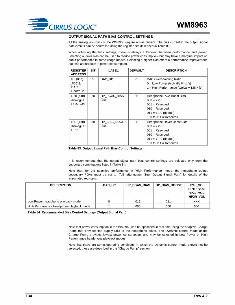
WM8963
134 Rev 4.2
OUTPUT SIGNAL PATH BIAS CONTROL SETTINGS
All the analogue circuits of the WM8963 require a bias current. The bias current in the output signal
path circuits can be controlled using the register bits described in Table 83.
When adjusting the bias settings, there is always a trade-off between performance and power.
Selecting a lower bias can be used to reduce power consumption, but may have a marginal impact on
audio performance in some usage modes. Selecting a higher bias offers a performance improvement,
but also an increase in power consumption.
REGISTER
ADDRESS
BIT LABEL DEFAULT DESCRIPTION
R6 (06h)
ADC &
DAC
Control 2
0 DAC_HP 0 DAC Oversampling Ratio
0 = Low Power (typically 64 x fs)
1 = High Performance (typically 128 x fs)
R68 (44h)
Analogue
PGA Bias
2:0 HP_PGAS_BIAS
[2:0]
011 Headphone PGA Boost Bias
000 = x 2.0
001 = Reserved
010 = Reserved
011 = x 1.0 (default)
100 to 111 = Reserved
R71 (47h)
Analogue
HP 2
2:0 HP_BIAS_BOOST
[2:0]
011 Headphone Driver Boost Bias
000 = x 2.0
001 = Reserved
010 = Reserved
011 = x 1.0 (default)
100 to 111 = Reserved
Table 83 Output Signal Path Bias Control Settings
It is recommended that the output signal path bias control settings are selected only from the
supported combinations listed in Table 84.
Note that, for the specified performance in ‘High Performance’ mode, the headphone output
secondary PGAs must be set to -7dB attenuation. See “Output Signal Path” for details of the
associated registers.
DESCRIPTION DAC_HP HP_PGAS_BIAS HP_BIAS_BOOST HP1L_VOL,
HP1R_VOL,
HP2L_VOL,
HP2R_VOL
Low Power headphone playback mode 0 011 011 XXX
High Performance headphone playback mode 1 000 000 000
Table 84 Recommended Bias Control Settings (Output Signal Path)
Note that power consumption in the WM8963 can be optimised in real time using the adaptive Charge
Pump that provides the supply rails to the headphone driver. The Dynamic control mode of the
Charge Pump provides lowest power consumption, and may be selected in Low Power or High
Performance headphone playback modes.
Note that there are some operating conditions in which the Dynamic control mode should not be
selected; these are described in the “Charge Pump” section.

WM8963
Rev 4.2 135
DIGITAL AUDIO INTERFACE
The digital audio interface is used for inputting DAC data to the WM8963 and outputting ADC data
from it. The digital audio interface uses four pins:
ADCDAT: ADC data output
DACDAT: DAC data input
LRCLK: Left/Right data alignment clock
BCLK: Bit clock, for synchronisation
The clock signals BCLK and LRCLK can be outputs when the WM8963 operates as a master, or
inputs when it is a slave (see “Master and Slave Mode Operation”, below).
Four different audio data formats are supported:
Left justified
Right justified
I2S
DSP mode
All four of these modes are MSB first. Data words are encoded in 2’s complement format. Each of the
audio interface modes is described in the following sections. Refer to the “Signal Timing
Requirements” section for timing information.
Time Division Multiplexing (TDM) is available in all four data format modes. The WM8963 can be
programmed to send and receive data in one of two time slots.
PCM operation is supported using the DSP mode.
MASTER AND SLAVE MODE OPERATION
The WM8963 digital audio interface can operate as a master or slave as shown in Figure 39 and
Figure 40.
WM8963 ADCDAT
LRCLK
DACDAT
BCLK
Processor
WM8963 ProcessorADCDAT
LRCLK
DACDAT
BCLK
Figure 39 Master Mode Figure 40 Slave Mode
The Audio Interface output control is illustrated above. The MSTR control register determines whether
the WM8963 generates the clock signals. The MSTR register field is defined in Table 85.
REGISTER
ADDRESS
BIT LABEL DEFAULT DESCRIPTION
R7 (07h)
Audio
Interface 0
6 MSTR 0 Audio Interface Mode Select
0 = Slave mode
1 = Master mode
Table 85 Audio Interface Master/Slave Control

WM8963
136 Rev 4.2
OPERATION WITH TDM
Time division multiplexing (TDM) allows multiple devices to transfer data simultaneously on the same
bus. The WM8963 ADCs and DACs support TDM in master and slave modes for all data formats and
word lengths. TDM is enabled and configured using register bits defined in the “Digital Audio Interface
Control” section.
WM8963 Processor
WM8963 or
Similar
CODEC ADCDAT
LRCLK
DACDAT
BCLK
ADCDAT
LRCLK
DACDAT
BCLK
WM8963 Processor
WM8963 or
Similar
CODEC ADCDAT
LRCLK
DACDAT
BCLK
ADCDAT
LRCLK
DACDAT
BCLK
Figure 41 TDM with WM8963 as Master Figure 42 TDM with Other CODEC as Master
WM8963 Processor
WM8963 or
Similar
CODEC ADCDAT
LRCLK
DACDAT
BCLK
ADCDAT
LRCLK
DACDAT
BCLK
Figure 43 TDM with Processor as Master
Note: The WM8963 is a 24-bit device. If the user operates the WM8963 in 32-bit mode then the 8
LSBs will be ignored on the receiving side and not driven on the transmitting side. It is therefore
recommended to add a pull-down resistor, if necessary, to the DACDAT line and the ADCDAT line in
TDM mode.

WM8963
Rev 4.2 137
BCLK FREQUENCY
The BCLK frequency is controlled relative to SYSCLK by the BCLK_DIV divider. Internal clock divide
and phase control mechanisms ensure that the BCLK and LRCLK edges will occur in a predictable
and repeatable position relative to each other and relative to the data for a given combination of
DAC/ADC sample rate and BCLK_DIV settings.
BCLK_DIV is defined in the “Digital Audio Interface Control” section. See also “Clocking and Sample
Rates” section for more information.
AUDIO DATA FORMATS (NORMAL MODE)
In Right Justified mode, the LSB is available on the last rising edge of BCLK before a LRCLK
transition. All other bits are transmitted before (MSB first). Depending on word length, BCLK
frequency and sample rate, there may be unused BCLK cycles after each LRCLK transition.
nn-1n-2321 nn-1n-2321
LEFT CHANNEL RIGHT CHANNEL
MSB LSBInput Word Length (WL)
1/fs
LRCLK
BCLK
DACDAT/
ADCDAT
Figure 44 Right Justified Audio Interface (assuming n-bit word length)
In Left Justified mode, the MSB is available on the first rising edge of BCLK following a LRCLK
transition. The other bits up to the LSB are then transmitted in order. Depending on word length,
BCLK frequency and sample rate, there may be unused BCLK cycles before each LRCLK transition.
nn-1n-2321 nn-1n-2321
LEFT CHANNEL RIGHT CHANNEL
MSB LSBInput Word Length (WL)
1/fs
LRCLK
BCLK
DACDAT/
ADCDAT
Figure 45 Left Justified Audio Interface (assuming n-bit word length)
In I2S mode, the MSB is available on the second rising edge of BCLK following a LRCLK transition.
The other bits up to the LSB are then transmitted in order. Depending on word length, BCLK
frequency and sample rate, there may be unused BCLK cycles between the LSB of one sample and
the MSB of the next.

WM8963
138 Rev 4.2
nn-1n-2321 nn-1n-2321
LEFT CHANNEL RIGHT CHANNEL
MSB LSBInput Word Length (WL)
1/fs
LRCLK
BCLK
DACDAT/
ADCDAT
1 BCLK 1 BCLK
Figure 46 I2S Justified Audio Interface (assuming n-bit word length)
In DSP mode, the left channel MSB is available on either the 1st (mode B) or 2nd (mode A) rising edge
of BCLK (selectable by LRCLK_INV) following a rising edge of LRCLK. Right channel data
immediately follows left channel data. Depending on word length, BCLK frequency and sample rate,
there may be unused BCLK cycles between the LSB of the right channel data and the next sample.
In device master mode, the LRC output will resemble the frame pulse shown in Figure 47 and Figure
48. In device slave mode, Figure 49 and Figure 50, it is possible to use any length of frame pulse less
than 1/fs, providing the falling edge of the frame pulse occurs greater than one BCLK period before
the rising edge of the next frame pulse.
nn-1n-2321 nn-1n-2321
LEFT CHANNEL RIGHT CHANNEL
MSB LSBInput Word Length (WL)
1/fs
LRCLK
BCLK
DACDAT/
ADCDAT
1 BCLK
1/2fs
Figure 47 DSP Mode Audio Interface (mode A, LRCLK_INV=0, Master)
nn-1n-2321 nn-1n-2321
LEFT CHANNEL RIGHT CHANNEL
MSB LSBInput Word Length (WL)
1/fs
LRCLK
BCLK
DACDAT/
ADCDAT
1/2fs
Figure 48 DSP Mode Audio Interface (mode B, LRCLK_INV=1, Master)

WM8963
Rev 4.2 139
nn-1n-2321 nn-1n-2321
LEFT CHANNEL RIGHT CHANNEL
MSB LSBInput Word Length (WL)
1/fs
LRCLK
BCLK
DACDAT/
ADCDAT
1 BCLK
Falling edge can occur anywhere in this area
1 BCLK
Figure 49 DSP Mode Audio Interface (mode A, LRCLK_INV=0, Slave)
nn-1n-2321 nn-1n-2321
LEFT CHANNEL RIGHT CHANNEL
MSB LSBInput Word Length (WL)
1/fs
LRCLK
BCLK
DACDAT/
ADCDAT
1 BCLK 1 BCLK
Falling edge can occur anywhere in this area
Figure 50 DSP Mode Audio Interface (mode B, LRCLK_INV=1, Slave)
PCM operation is supported in DSP interface mode. WM8963 ADC data that is output on the Left
Channel will be read as mono PCM data by the receiving equipment. Mono PCM data received by the
WM8963 will be treated as Left Channel data. This data may be routed to the Left/Right DACs as
described in the “Digital Mixing” section.
AUDIO DATA FORMATS (TDM MODE)
TDM is supported in master and slave mode and is enabled by register bits AIFADC_TDM_MODE
and AIFDAC_TDM_MODE. All audio interface data formats support time division multiplexing (TDM)
for ADC and DAC data.
Two time slots are available (Slot 0 and Slot 1), selected by register bits AIFADC_TDM_SLOT and
AIFDAC_TDM_SLOT which control time slots for the ADC data and the DAC data.
When TDM is enabled, the ADCDAT pin will be tri-stated immediately before and immediately after
data transmission, to allow another ADC device to drive this signal line for the remainder of the
sample period. Note that it is important that two ADC devices do not attempt to drive the data pin
simultaneously. A short circuit may occur if the transmission time of the two ADC devices overlap with
each other. See “Audio Interface Timing” for details of the ADCDAT output relative to BCLK signal.
Note that it is possible to ensure a gap exists between transmissions by setting the transmitted word
length to a value higher than the actual length of the data. For example, if 32-bit word length is
selected where only 24-bit data is available, then the WM8963 interface will tri-state after transmission
of the 24-bit data, ensuring a gap after the WM8963’s TDM slot.
When TDM is enabled, BCLK frequency must be high enough to allow data from both time slots to be
transferred. The relative timing of Slot 0 and Slot 1 depends upon the selected data format as shown
in Figure 51 to Figure 55.

WM8963
140 Rev 4.2
SLOT 0
LEFT CHANNEL RIGHT CHANNEL
1/fs
LRCLK
BCLK
DACDAT/
ADCDATSLOT 1 SLOT 0 SLOT 1
Figure 51 TDM in Right-Justified Mode
LEFT CHANNEL RIGHT CHANNEL
1/fs
LRCLK
BCLK
DACDAT/
ADCDATSLOT 0 SLOT 1 SLOT 0 SLOT 1
Figure 52 TDM in Left-Justified Mode
LEFT CHANNEL RIGHT CHANNEL
1/fs
LRCLK
BCLK
DACDAT/
ADCDAT
1 BCLK 1 BCLK
SLOT 0 SLOT 1 SLOT 0 SLOT 1
Figure 53 TDM in I2S Mode
1/fs
LRCLK
BCLK
DACDAT/
ADCDAT
1 BCLK
SLOT 0 LEFT SLOT 0 RIGHT SLOT 1 LEFT SLOT 1 RIGHT
Falling edge can occur anywhere in this area
1 BCLK
Figure 54 TDM in DSP Mode A

WM8963
Rev 4.2 141
1/fs
LRCLK
BCLK
DACDAT/
ADCDAT
1 BCLK
SLOT 0 LEFT SLOT 0 RIGHT SLOT 1 LEFT SLOT 1 RIGHT
Falling edge can occur anywhere in this area
1 BCLK
Figure 55 TDM in DSP Mode B
DIGITAL AUDIO INTERFACE CONTROL
The register bits controlling audio data format, word length, left/right channel data configuration and
TDM are summarised in Table 86.
REGISTER
ADDRESS
BIT LABEL DEFAULT DESCRIPTION
R5 (05h)
ADC and
DAC
Control 1
6 ADCR_DAT_IN
V
0 Right ADC Invert
0 = Right ADC output not inverted
1 = Right ADC output inverted
5 ADCL_DAT_INV 0 Left ADC Invert
0 = Left ADC output not inverted
1 = Left ADC output inverted
R6 (06h)
ADC and
DAC
Control 2
6 DACR_DAT_IN
V
0 Right DAC Invert
0 = Right DAC input not inverted
1 = Right DAC input inverted
5 DACL_DAT_INV 0 Left DAC Invert
0 = Left DAC input not inverted
1 = Left DAC input inverted
R7 (07h)
Audio
Interface
0
12 AIFDAC_TDM_
MODE
0 DAC TDM Mode Select
0 = Normal DACDAT operation (1 stereo
slot)
1 = TDM enabled on DACDAT (2 stereo
slots)
11 AIFDAC_TDM_
SLOT
0 DACDAT TDM Slot Select
0 = DACDAT data input on slot 0
1 = DACDAT data input on slot 1
10 AIFADC_TDM_
MODE
0 ADC TDM Mode Select
0 = Normal ADCDAT operation (1 stereo
slot)
1 = TDM enabled on ADCDAT (2 stereo
slots)
9 AIFADC_TDM_
SLOT
0 ADCDAT TDM Slot Select
0 = ADCDAT data input on slot 0
1 = ADCDAT data input on slot 1
8 ADC_LRSWAP 0 Swap left/right ADC data on the interface
0 = Normal
1 = ADCDAT channels swapped
7 BCLK_INV 0 BCLK Invert
0 = BCLK not inverted
1 = BCLK inverted
5 DAC_LRSWAP 0 Swap left/right DAC data on the interface
0 = Normal
1 = DACDAT channels swapped

WM8963
142 Rev 4.2
REGISTER
ADDRESS
BIT LABEL DEFAULT DESCRIPTION
4 LRCLK_INV 0 Right, left and I2S modes – LRCLK polarity
0 = normal LRCLK polarity
1 = invert LRCLK polarity
DSP Mode – mode A/B select
0 = MSB is available on 2nd BCLK rising
edge after LRCLK rising edge (mode A)
1 = MSB is available on 1st BCLK rising
edge after LRCLK rising edge (mode B)
3:2 WL [1:0] 10 Digital Audio Interface Word Length
00 = 16 bits
01 = 20 bits
10 = 24 bits
11 = 32 bits
Note - see “Companding” for the selection of
8-bit mode.
1:0 FMT [1:0] 10 Digital Audio Interface Format
00 = Right justified
01 = Left justified
10 = I2S Format
11 = DSP Mode
Table 86 Digital Audio Interface Data Control
AUDIO INTERFACE TRI-STATE
Register bit AIF_TRI can be used to tri-state the audio interface pins as described in Table 87. All
digital audio interface pins will be tri-stated by this function, regardless of the state of other registers
which control these pin configurations.
REGISTER
ADDRESS
BIT LABEL DEFAULT DESCRIPTION
R24 (18h)
Additional
Control (2)
3 AIF_TRI 0 Audio Interface Tristate
0 = Audio interface pins operate normally
1 = ADCDAT is tri-stated; BCLK and LRCLK
are set as inputs
Table 87 Digital Audio Interface Tri-State Control
BCLK AND LRCLK CONTROL
The audio interface can be programmed to operate in master mode or slave mode using the MSTR
register bit.
In master mode, the BCLK and LRCLK signals are generated by the WM8963 when any of the ADCs
or DACs is enabled. In slave mode, the BCLK and LRCLK clock outputs are disabled by default to
allow another digital audio interface to drive these pins. Refer to “Clocking and Sample Rates” for
specific operating constraints in this configuration.

WM8963
Rev 4.2 143
REGISTER
ADDRESS
BIT LABEL DEFAULT DESCRIPTION
R7 (07h)
Audio
Interface 0
6 MSTR 0 Audio Interface Mode Select
0 = Slave mode
1 = Master mode
R8 (08h)
Clocking2
3:0 BCLK_DIV 0100 BCLK Rate
0000 = DSPCLK
0001 = Reserved
0010 = DSPCLK / 2
0011 = DSPCLK / 3
0100 = DSPCLK / 4 (default)
0101 = Reserved
0110 = DSPCLK / 6
0111 = DSPCLK / 8
1000 = Reserved
1001 = DSPCLK / 12
1010 = DSPCLK / 16
1011 = DSPCLK / 24
1100 = Reserved
1101 = DSPCLK / 32
1110 = DSPCLK / 32
1111 = DSPCLK / 32
R14 (0Eh)
Audio
Interface 2
10:0 AIF_RATE
[10:0]
040h LRCLK Rate
LRCLK clock output =
BCLK / AIF_RATE
Integer (LSB = 1)
Valid from 4..2047
Default (040h) = 64 BCLKs per LRCLK
Table 88 Digital Audio Interface Clock Control
COMPANDING
The WM8963 supports A-law and -law companding on both transmit (ADC) and receive (DAC) sides
as shown in Table 89.
REGISTER
ADDRESS
BIT LABEL DEFAULT DESCRIPTION
R9 (09h)
Audio
Interface 1
4 DAC_COMP 0 DAC Companding Enable
0 = disabled
1 = enabled
3 DAC_COMPMODE 0 DAC Companding Type
0 = µ-law
1 = A-law
2 ADC_COMP 0 ADC Companding Enable
0 = disabled
1 = enabled
1 ADC_COMPMODE 0 ADC Companding Type
0 = µ-law
1 = A-law
Table 89 Companding Control

WM8963
144 Rev 4.2
Companding involves using a piecewise linear approximation of the following equations (as set out by
ITU-T G.711 standard) for data compression:
-law (where =255 for the U.S. and Japan):
F(x) = ln( 1 + |x|) / ln( 1 + ) -1 ≤ x ≤ 1
A-law (where A=87.6 for Europe):
F(x) = A|x| / ( 1 + lnA) x ≤ 1/A
F(x) = ( 1 + lnA|x|) / (1 + lnA) 1/A ≤ x ≤ 1
The companded data is also inverted as recommended by the G.711 standard (all 8 bits are inverted
for -law, all even data bits are inverted for A-law). The data will be transmitted as the first 8 MSBs of
data.
Companding converts 13 bits (-law) or 12 bits (A-law) to 8 bits using non-linear quantization. This
provides greater precision for low amplitude signals than for high amplitude signals, resulting in a
greater usable dynamic range than 8 bit linear quantization. The companded signal is an 8-bit word
comprising sign (1 bit), exponent (3 bits) and mantissa (4 bits).
8-bit mode is selected whenever DAC_COMP=1 or ADC_COMP=1. The use of 8-bit data allows
samples to be passed using as few as 8 BCLK cycles per LRCLK frame. When using DSP mode B, 8-
bit data words may be transferred consecutively every 8 BCLK cycles.
8-bit mode (without Companding) may be enabled by setting DAC_COMPMODE=1 or
ADC_COMPMODE=1, when DAC_COMP=0 and ADC_COMP=0.
BIT7 BIT[6:4] BIT[3:0]
SIGN EXPONENT MANTISSA
Table 90 8-bit Companded Word Composition
u-law Companding
0
20
40
60
80
100
120
0 0.1 0.2 0.3 0.4 0.5 0.6 0.7 0.8 0.9 1
Normalised Input
Co
mp
an
ded
Ou
tpu
t
0
0.1
0.2
0.3
0.4
0.5
0.6
0.7
0.8
0.9
1
No
rmali
sed
Ou
tpu
t
Figure 56 µ-Law Companding

WM8963
Rev 4.2 145
A-law Companding
0
20
40
60
80
100
120
0 0.2 0.4 0.6 0.8 1
Normalised Input
Co
mp
an
ded
Ou
tpu
t
0
0.1
0.2
0.3
0.4
0.5
0.6
0.7
0.8
0.9
1
No
rmali
sed
Ou
tpu
t
Figure 57 A-Law Companding
LOOPBACK
Setting the LOOPBACK register bit enables digital loopback. When this bit is set, the ADC digital data
output is routed to the DAC digital data input path. The digital audio interface input (DACDAT) is not
used when LOOPBACK is enabled.
REGISTER
ADDRESS
BIT LABEL DEFAULT DESCRIPTION
R9 (09h)
Audio
Interface (2)
0 LOOPBACK 0 Digital Loopback Function
0 = No loopback
1 = Loopback enabled (ADC data output
is directly input to DAC data input).
Table 91 Loopback Control
Note: When the digital sidetone is enabled, ADC data will also be added to DAC digital data input
path within the Digital Mixing circuit. This applies regardless of whether LOOPBACK is enabled.

WM8963
146 Rev 4.2
CLOCKING AND SAMPLE RATES
The internal clocks for the WM8963 are all derived from a common internal clock source, SYSCLK.
This clock is the reference for the ADCs, DACs, DSP core functions, digital audio interface, Class D
switching amplifier, DC servo control and other internal functions.
SYSCLK can either be derived directly from MCLK, or may be generated from the Frequency Locked
Loop (FLL), or from the crystal oscillator. Many commonly-used audio sample rates can be derived
directly from typical MCLK frequencies; the FLL provides additional flexibility for a wide range of
reference frequencies. To avoid audible glitches, all clock configurations must be set up before
enabling playback. The FLL can be used to generate a free-running clock in the absence of an
external reference source; see “Frequency Locked Loop (FLL)” for further details of the FLL circuit.
The WM8963 supports automatic clocking configuration. The programmable dividers associated with
the ADCs, DACs, DSP core functions, Class D switching and DC servo are configured automatically,
with values determined from the MCLK_RATE and SAMPLE_RATE fields. The user must also
configure the OPCLK (if required), the TOCLK (if required) and the digital audio interface.
ADC/DAC oversample rates of 64fs or 128fs are supported (based on a 48kHz sample rate).
A 256kHz clock, supporting a number of internal functions, is derived from SYSCLK.
The Class D switching amplifier and DC servo control circuits are clocked from SYSCLK.
A GPIO Clock, OPCLK, can be derived from SYSCLK and output on the GPIO2 pin to provide
clocking to other devices. This clock is enabled by OPCLK_ENA and controlled by OPCLK_DIV.
A slow clock, TOCLK, is used to set the timeout period for volume updates when zero-cross detect is
used. This clock is enabled by TOCLK_ENA and controlled by TOCLK_DIV. A de-bounce clock,
DBCLK, is used to control the de-bouncing of button/accessory detect GPIO input and selected
interrupt inputs. This clock is enabled automatically whenever GPIO or interrupt de-bouncing is
selected. The de-bounce clock frequency is controlled by DBCLK_DIV.
In master mode, BCLK is derived from DSPCLK via a programmable divider set by BCLK_DIV. In
master mode, the LRCLK is derived from BCLK via a programmable divider AIF_RATE.
In Slave mode, BCLK and LRCLK are inputs to the WM8963, allowing another digital audio interface
to drive these pins. See the “BCLK and LRCLK Control” sub-section for specific operating constraints
in this configuration.
The control registers associated with Clocking and Sample Rates are shown in Table 94 to Table 99.
The overall clocking scheme for the WM8963 is illustrated in Figure 58.

WM8963
Rev 4.2 147
MCLK
f/N
SYSCLK_DIV[1:0]
00 = MCLK
01 = MCLK / 2
10 = MCLK / 4
f/N
DACf/N
SYSCLK
(12.288MHz max)
f/N Class D switching clock
f/N
256kHz clock to
Write Sequencer
and other circuits
Volume update timeoutf/N
DSP Coref/N
f/2 or f/3
MCLK
MCLK_SRC andOSC_MCLK_SRC select the master clock source (MCLK pin, FLL, GPIO6 pin,
or Oscillator). The GPIO6 or Oscillator sources, when selected, are divided by OSC_DIV. The
selected source is used to derive SYSCLK, DSPCLK and other clocks automatically.
Automatic Clocking Configuration
Internal clocks are derived from the master clock source . These are configured using
MANUAL_MODE, SAMPLE_RATE, MCLK_RATE, ADC_HP and DAC_HP.
DSP Clock
Clocking for the Digital Audio Interface and many of the DSP functions is derived from DSPCLK.
The master clock source is divided by DSPCLK_DIV to derive DSPCLK. The DSPCLK_DIV
divider is configured automatically. Clocking for the DAC ReTune, DAC HPF, VSS and MBC
functions is derived from DSP2CLK.
SYSCLK
Other internal clocks are derived from SYSCLK. The master clock source is divided by
SYSCLK_DIV to derive SYSCLK. The SYSCLK_DIV divider is configured automatically.
SYSCLK is enabled by SYSCLK_ENA.
ADC / DAC Clocks
The ADC clocks are controlled by ADCSYS_CLK_DIV and ADC_HP. The DAC clocks are
controlled by DACSYS_CLK_DIV and DAC_HP. The dividers ADCSYS_CLK_DIV and
DACSYS_CLK_DIV are configured automatically.
Class D Switching
Class D switching rate is set by CLASSD_CLK_DIV. The clock frequency is automatically set to
around 768kHz.
256kHz Clock
The 256k clock for internal functions is set automatically by F256KCLK_DIV.
OPCLK Output
GPIO output clock frequency is set by OPCLK_DIV.
TOCLK, DBCLK Control
The slow clock for volume update timeout is enabled by TOCLK_ENA; the frequency is
controlled by TOCLK_DIV. Clocking for interrupt de-bounce is enabled automatically when
required; the frequency is set by DBCLK_DIV.
Digital Audio Interface Control
BCLK rate is set by BCLK_DIV in master mode. BCLK rate must be high enough to support the
ADC and DAC sample rates. LRCLK rate is set by AIF_RATE in master mode.
MCLK
f/N Interrupt de-bounce clock
FLL
BCLK_DIV[3:0]
0000 = DSPCLK
0001 = Reserved
0010 = DSPCLK/ 2
0011 = DSPCLK/ 3
0100 = DSPCLK/ 4
0101 = Reserved
0110 = DSPCLK/ 6
0111 = DSPCLK/ 8
1000 = Reserved
1001 = DSPCLK/ 12
1010 = DSPCLK/ 16
1011 = DSPCLK/ 24
1100 = Reserved
1101 = DSPCLK/ 32
1110 = DSPCLK/ 32
1111 = DSPCLK/ 32
f/N LRCLK
BCLK
MASTER
MODE
CLOCK
OUTPUTSf/N
DSPCLK_DIV[1:0]
00 = MCLK
01 = MCLK / 2
10 = MCLK / 4
DSPCLK (24.576MHz max)
Automatic DSP
Clocking Control
SAMPLE_RATE [2:0]
MCLK_RATE [3:0]
In Automatic DSP Clocking Mode,
the DAC, ADC, 256kHz, DC Servo
and Class D clocks are configured
automatically according to
SAMPLE_RATE, SYSCLK_RATE,
DAC_HP and ADC_HP.
DAC_HP
ADC_HP
MCLK_SRC SYSCLK_ENA
AIF_RATE [10:0]
DACSYS_CLK_DIV
[2:0]ADCSYS_CLK_DIV
[2:0]
CLASSD_CLK_DIV [2:0]
F256KCLK_DIV
[5:0]
TOCLK_ENA
TOCLK_DIV
[2:0]
DBCLK_DIV
[2:0]
BCLK_DIV [3:0]
DSP Coref/NDSP2CLK (49.152MHz max)
ADC
f/2
GPIO Clock Outputf/N
OPCLK_DIV[2:0]
000 = SYSCLK
001 = SYSCLK / 2
010 = SYSCLK / 3
011 = SYSCLK / 4
100 = SYSCLK / 6
101 = SYSCLK / 8
110 = SYSCLK / 12
111 = SYSCLK / 16
OPCLK_ENA
GPIO6f/N
OSC_DIV
00 = Divide by 1
01 = Divide by 2
10 = Divide by 4
11 = Reserved
MCLK_SRCOscillator
OSC_MCLK_SRC
Figure 58 SYSCLK and Internal Clocking Scheme

WM8963
148 Rev 4.2
SYSCLK CONTROL
The MCLK_SRC and OSC_MCLK_SRC registers are used to select the source for MCLK. The source
may be either the MCLK pin, FLL, GPIO6 pin, or Oscillator. The GPIO6 or Oscillator sources, when
selected, are controlled by the OSC_DIV divider.
The selected source may be adjusted by the programmable divider SYSCLK_DIV; this is configured
automatically by the WM8963 to ensure that SYSCLK <= 12.288MHz. (Note that the SYSCLK_DIV
divider is a read-only register; it cannot be written to.)
The MCLK_SRC register is controlled automatically under certain circumstances, as described below.
The associated control register, CLKREG_OVD, is defined in the following section (“Automatic
Clocking Configuration”).
When a logic 1 is applied on the GPIO5 pin, the MCLK_SRC register is set to 01b, selecting FLL as
the source. In this case, the MCLK_SRC register is locked to prevent accidental writes to this register.
The MCLK_SRC register can be unlocked by setting the CLKREG_OVD bit.
When a logic 0 is applied on the GPIO5 pin, the MCLK_SRC register defaults to 00b, selecting MCLK
as the source. In this case, the default (00b) is selected on the falling edge of GPIO5; other settings
can then be selected by writing to the MCLK_SRC register as normal.
Note that it is important that the GPIO5 input is held in a defined logic state (logic ‘0’ or logic ‘1’) during
start-up; it must not be left floating. If normal GPIO functionality is required on the GPIO5 pin, then the
CLKREG_OVD bit must be set to ‘1’ in order to select normal read/write control of all the clocking
registers, and to permit GPIO functions. The GPIO5 pin must be held in a defined logic state (logic ‘0’
or logic ‘1’) whenever the pin is configured as an input, including whenever CLKREG_OVD = 0
(default).
See “Internal / External Clock Generation” for more details of the FLL and Crystal Oscillator.
The SYSCLK signal is enabled by register bit SYSCLK_ENA. This bit should be set to 0 when
reconfiguring clock sources. Note that, when reconfiguring or disabling SYSCLK, the ADCs and DACs
must be disabled before setting SYSCLK_ENA=0.
The following operating frequency limits are recommended when configuring SYSCLK. Failure to
observe these limits may result in degraded noise performance.
MCLK 3MHz
If DAC_HP = 1, then MCLK 6MHz
The valid clocking ratios for DAC and/or ADC operation are identified in Table 92. See also Table 93
for details of the supported functions for each combination of Sample Rate and MCLK / fs ratio.
Note that, in some cases, the combination of Sample Rate and MCLK / fs ratio has a dependency on
the DCVDD supply voltage. The marked (*) combinations are only valid for DCVDD 1.7V.
SAMPLE
RATE (kHz)
MCLK RATE (MCLK / fs ratio)
64 128 192 256 384 512 768 1024 1536 3072 6144
8 1 2 3 4 5 6 6 6 6 6 6*
11.025 1 2 3 4 5 6 6 6 6 6*
12 1 2 3 4 5 6 6 6 6 6*
16 1 2 3 4 5 6 6 6 6 6*
22.05 1 2 3 4 5 6 6 6 6*
24 1 2 3 4 5 6 6 6 6*
32 1 2 3 4 5 6 6 6* 6*
44.1 1 2 3 4 5 6 5* 6*
48 1 2 3 4 5 6 5* 6*
88.2 1 2 3 4 3* 4*
96 1 2 3 4 3* 4*
Note - the clocking configurations marked (*) are only valid for DCVDD 1.7V.
Table 92 MCLK / Sample Rate Availability

WM8963
Rev 4.2 149
CODE DAC/ADC Configuration ADC Signal Path
Enhancements
DAC Signal Path Enhancements
HPF,
LPF/HPF,
DF1 Filter,
3D Surround,
Dynamic Range
Control (DRC)
Dynamic Range
Control (DRC)
5-band EQ Virtual Surround
Sound (VSS),
ReTune,
DAC HPF,
Multiband
Compressor (MBC)
1 Mono DAC
2 Stereo DAC
3 Stereo DAC
4 Stereo CODEC
or Stereo DAC
5 Stereo CODEC
6 Stereo CODEC
Table 93 DAC/ADC and Audio Enhancements Availability
The supported MCLK frequency range is defined in the “Signal Timing Requirements”.
The MCLK / fs ratio is set using the MCLK_RATE register. See “Automatic Clocking Configuration” for
details of this register.
The MCLK and SYSCLK control register fields are defined in Table 94.
REGISTER
ADDRESS
BIT LABEL DEFAULT DESCRIPTION
R4 (04h)
Clocking1
2:1 SYSCLK_DIV 00 SYSCLK Divider
00 = MCLK
01 = MCLK / 2
10 = MCLK / 4
11 = Reserved
This field is for read-back only; it is set
automatically and cannot be adjusted.
Note that the division is applied to the
selected MCLK source, including the
FLL or Oscillator, when applicable.
R8 (08h)
Clocking2
10:9 MCLK_SRC 00 MCLK source select
00 = MCLK pin
01 = FLL output
10 = GPIO6 or Oscillator (selected by
OSC_MCLK_SRC)
11 = Reserved
If CLKREG_OVD = 0, then MCLK_SRC
is controlled by the GPIO5 pin.
If CLKREG_OVD = 0 and GPIO5 = 1,
then MCLK_SRC = 01 (FLL) and
MCLK_SRC cannot be changed by the
Control Interface.
If CLKREG_OVD = 0 and GPIO5 = 0,
then MCLK_SRC = 00 (MCLK) by
default, but the value can be changed
via the Control Interface.
If CLKREG_OVD = 1 then MCLK_SRC
= 00 (MCLK) by default, but the value
can be changed via the Control
Interface.
5 SYSCLK_ENA 1 SYSCLK enable
0 = Disabled
1 = Enabled

WM8963
150 Rev 4.2
REGISTER
ADDRESS
BIT LABEL DEFAULT DESCRIPTION
R125 (7Dh)
Analogue
Clocking2
4:3 OSC_DIV 01 GPIO6 / Oscillator to MCLK divider
00 = Divide by 1
01 = Divide by 2
10 = Divide by 4
11 = Reserved
R152 (98h)
Analogue
Clocking 4
4 OSC_MCLK_SR
C
0 GPIO6 / Oscillator to MCLK source
0 = Oscillator
1 = GPIO6
This field selects the MCLK source,
when MCLK_SRC =10.
Table 94 MCLK and SYSCLK Control
AUTOMATIC CLOCKING CONFIGURATION
The WM8963 supports a wide range of standard audio sample rates from 8kHz to 96kHz. The
Automatic Clocking Configuration mode simplifies the configuration of the clock dividers in the
WM8963 by deriving most of the necessary parameters from a minimum number of user registers.
In Automatic mode, the SAMPLE_RATE field selects the sample rate, fs, of the ADC and DAC. The
SAMPLE_RATE_INT_MODE bit should be set according to the selected SAMPLE_RATE, as
described in Table 95. Note that, in Automatic mode, the same sample rate always applies to the ADC
and DAC.
In Automatic mode, the MCLK_RATE field must be set according to the ratio of MCLK to fs. (Note that
the MCLK source is selected by MCLK_SRC - see Table 94.)
Selectable modes of ADC / DAC operation are available using the ADC_HP and DAC_HP register
bits. The automatic clocking configuration uses DAC_HP to determine the applicable clock divider
settings.
The WM8963 is designed to support specific internal and external clocking configurations. Under
default conditions, the GPIO5 pin has control over selected clocking registers, and normal read/write
access to some registers is not supported. When the CLKREG_OVD register is set to 1, the affected
clocking registers are controlled as normal via the Control Interface. The registers that are affected by
CLKREG_OVD are noted in Table 100.
REGISTER
ADDRESS
BIT LABEL DEFAULT DESCRIPTION
R6 (06h)
ADC and
DAC
Control 2
0 DAC_HP 0 DAC Oversampling Ratio
0 = Low Power (typically 64 x fs)
1 = High Performance (typically 128 x fs)
R8 (08h)
Clocking2
11 CLKREG_OVD 0 Clock Configuration Override
0 = MCLK_SRC, OSC_ENA and
CLKOUT5_SEL registers are controlled
by the GPIO5 pin; CLKOUT2_DIV and
CLKOUT5_DIV registers are locked to
fixed values.
1 = Clocking registers are controlled as
normal via Control Interface.
This bit must be set to 1 to support GPIO
functionality on GPIO5.
R23 (17h)
Additional
Control (1)
5 ADC_HP 0 ADC Oversampling Ratio
0 = Low Power (typically 64 x fs)
1 = High Performance (typically 128 x fs)
R27 (1Bh)
Additional
Control (3)
4 SAMPLE_RATE
_INT_MODE
1 Selects the Integer or Fractional value of
the SAMPLE_RATE register.
0 = 11.025k, 22.05k, 44.1k or 88.2kHz
1 = 8k, 12k, 16k, 24k, 32k, 48k or 96kHz

WM8963
Rev 4.2 151
REGISTER
ADDRESS
BIT LABEL DEFAULT DESCRIPTION
2:0 SAMPLE_RATE
[2:0]
000 Selects the Sample Rate (fs)
000 = 44.1kHz, 48kHz
001 = 32kHz
010 = 22.05kHz, 24kHz
011 = 16kHz
100 = 11.025kHz, 12kHz
101 = 8kHz
110 = 88.2kHz, 96kHz
111 = Reserved
R56 (38h)
Clocking 4
4:1 MCLK_RATE
[3:0]
0011 Selects the MCLK / fs ratio.
(Note that the MCLK source is selected
by MCLK_SRC.)
0000 = 64
0001 = 128
0010 = 192
0011 = 256 (default)
0100 = 384
0101 = 512
0110 = 768
0111 = 1024
1000 = Reserved
1001 = 1536
1010 = 3072
1011 = 6144
If DAC ReTune, DAC HPF, VSS or MBC
is enabled, then MCLK_RATE must be
512 or higher.
Table 95 Automatic Clocking Configuration Control

WM8963
152 Rev 4.2
DSP, ADC, DAC CLOCK CONTROL
The clocking of the DSP is derived from MCLK. The clocking of the ADC and DAC circuits is derived
from SYSCLK. The associated dividers are configured automatically by the WM8963.
The DSP clocking rate is controlled by DSPCLK_DIV. In automatic clocking mode, this is configured
automatically by the WM8963 to ensure DSPCLK <= 24.576MHz. (Note that the DSPCLK_DIV divider
is a read-only register; it cannot be written to.)
The ADC clocking rate is controlled by ADCSYS_CLK_DIV. In automatic clocking mode, the WM8963
uses this divider to derive the most suitable SYSCLK / fs ratio, where fs is the ADC sampling rate.
The DAC clocking rate is controlled by DACSYS_CLK_DIV. In automatic clocking mode, the WM8963
uses this divider to derive the most suitable SYSCLK / fs ratio, where fs is the DAC sampling rate.
REGISTER
ADDRESS
BIT LABEL DEFAULT DESCRIPTION
R4 (04h)
Clocking 1
10:9 DSPCLK_DIV
[1:0]
00 DSP Clock Divider
00 = MCLK
01 = MCLK / 2
10 = MCLK / 4
11 = Reserved
This field is for read-back only; it is set
automatically and cannot be adjusted.
8:6 ADCSYS_CLK_
DIV [2:0]
000 ADC Sample Rate Divider
000 = SYSCLK
001 = Reserved
010 = SYSCLK / 2
011 = SYSCLK / 3
100 = SYSCLK / 4
101 = Reserved
110 = SYSCLK / 6
111= Reserved
This field is for read-back only; it is set
automatically and cannot be adjusted.
5:3 DACSYS_CLK_
DIV [2:0]
100 DAC Sample Rate Divider
000 = SYSCLK
001 = Reserved
010 = SYSCLK / 2
011 = SYSCLK / 3
100 = SYSCLK / 4
101 = Reserved
110 = SYSCLK / 6
111= Reserved
This field is for read-back only; it is set
automatically and cannot be adjusted.
Table 96 DSP, ADC, DAC Clock Control

WM8963
Rev 4.2 153
CLASS D, 256K, DC SERVO CLOCK CONTROL
The clocking of the Class D amplifier, DC Servo and other functions is derived from SYSCLK. The
associated dividers are configured automatically by the WM8963.
The Class D amplifier switching frequency is controlled by CLASSD_CLK_DIV. In automatic clocking
mode, the WM8963 uses this divider to generate a Class D clock that is approximately 768kHz. (Note
that there is an additional divide by two in the output stage producing a 384kHz switching frequency.)
A 256kHz clock is required for other circuits, including the Control Write Sequencer. In automatic
clocking mode, the WM8963 uses F256KCLK_DIV to generate a clock that is approximately 256kHz.
REGISTER
ADDRESS
BIT LABEL DEFAULT DESCRIPTION
R8 (08h)
Clocking2
8:6 CLASSD_CLK_
DIV [2:0]
111 Class D Clock Divider
000 = SYSCLK
001 = SYSCLK / 2
010 = SYSCLK / 3
011 = SYSCLK / 4
100 = SYSCLK / 6
101 = SYSCLK / 8
110 = SYSCLK / 12
111= SYSCLK / 16
This field is for read-back only; it is set
automatically and cannot be adjusted.
R30 (1Eh)
Clocking 3
6:1 F256KCLK_DIV
[5:0]
2Fh 256kHz Clock Divider
0d = SYSCLK
1d = SYSCLK / 2
2d = SYSCLK / 3
….
63d = SYSCLK / 64
This field is for read-back only; it is set
automatically and cannot be adjusted..
Table 97 Class D, 256k, DC Servo Clock Control
OPCLK CONTROL
A clock output (OPCLK) derived from SYSCLK may be output on the GPIO2 pin. This clock is enabled
by register bit OPCLK_ENA, and its frequency is controlled by OPCLK_DIV.
This output of this clock is also dependent upon the GPIO register settings described in the “General
Purpose Input/Output (GPIO)” section.

WM8963
154 Rev 4.2
REGISTER
ADDRESS
BIT LABEL DEFAULT DESCRIPTION
R25 (19h)
Pwr Mgmt
(1)
9 OPCLK_ENA 0 GPIO Clock Output Enable
0 = Disabled
1 = Enabled
R30 (1Eh)
Clocking 3
12:10 OPCLK_DIV
[2:0]
000 GPIO Output Clock Divider
000 = SYSCLK
001 = SYSCLK / 2
010 = SYSCLK / 3
011 = SYSCLK / 4
100 = SYSCLK / 6
101 = SYSCLK / 8
110 = SYSCLK / 12
111 = SYSCLK / 16
000 = SYSCLK / 16
Table 98 OPCLK Control
TOCLK, DBCLK CONTROL
A slow clock (TOCLK) is derived from the internally generated 256kHz clock to enable input de-
bouncing and volume update timeout functions. This clock is enabled by register bit TOCLK_ENA,
and its frequency is controlled by TOCLK_DIV.
A de-bounce clock, DBCLK, is used to control the de-bouncing of GPIO inputs and selected interrupt
inputs. This clock is enabled automatically whenever GPIO or interrupt de-bouncing is selected. The
de-bounce clock frequency is controlled by DBCLK_DIV.
REGISTER
ADDRESS
BIT LABEL DEFAULT DESCRIPTION
R23 (17h)
Additional
Control(1)
0 TOCLK_ENA 0 TOCLK Enable
0 = Disabled
1 = Enabled
R30 (1Eh)
Clocking 3
15:13 DBCLK_DIV
[2:0]
000 DBCLK Rate Divider
(divides the 256kHz clock; nominal
frequency is quoted in brackets)
000 = f / 256 (1kHz)
001 = f / 2048 (125Hz)
010 = f / 4096 (62.5Hz)
011 = f / 8192 (31.2Hz)
100 = f / 16384 (15.6Hz)
101 = f / 32768 (7.8Hz)
110 = f / 64536 (3.9Hz)
111 = f / 131072 (1.95Hz)
9:7 TOCLK_DIV
[2:0]
000 TOCLK Rate Divider
(divides the 256kHz clock; nominal
frequency is quoted in brackets)
000 = f / 256 (1kHz)
001 = f / 512 (500Hz)
010 = f / 1024 (250Hz)
011 = f / 2048 (125Hz)
100 = f / 4096 (62.5Hz)
101 = f / 8192 (31.2Hz)
110 = f / 16384 (15.6Hz)
111 = f / 32768 (7.8Hz)
Table 99 TOCLK, DBCLK Control

WM8963
Rev 4.2 155
BCLK AND LRCLK CONTROL
In master mode, BCLK is derived from DSPCLK via a programmable division set by BCLK_DIV.
In master mode, LRCLK is derived from BCLK via a programmable division set by AIF_RATE.
See “Digital Audio Interface Control” for details of these fields.
In Slave mode, BCLK/LRCLK should not be stopped whilst a DAC to Speaker playback path is active
unless SYSCLK is also stopped. Failure to meet this requirement may result in a DC output at the
speaker outputs, and possible speaker damage.
In Slave mode, if BCLK/LRCLK may stop during DAC to Speaker playback then it is recommended to
use a SYSCLK source that will also stop at the same time as BCLK/LRCLK. It is important to note that
the FLL will continue to run even when its input reference is removed; if the FLL is selected as the
SYSCLK source, then SYSCLK will not stop if BCLK/LRCLK is stopped.
If SYSCLK is stopped whenever BCLK/LRCLK is stopped, or if the audio interface is operating in
Master mode, then no specific action is required in relation to BCLK/LRCLK stopping.
If BCLK/LRCLK may stop during DAC to Speaker playback, with SYSCLK still running, then it is
recommended to disable the Speaker output (see “Output Signal Path”) before stopping
BCLK/LRCLK.
If it is not possible to change the WM8963 settings before BCLK/LRCLK are stopped (ie. the
BCLK/LRCLK inputs may stop unpredictably), then the DAC 2nd order HPF should be enabled in order
to remove DC offsets in the output signal. See “DAC Signal Path Enhancements” for details of this
feature.
CONTROL INTERFACE CLOCKING
Register map access is possible with or without a system clock (SYSCLK). The source for SYSCLK
may be either the MCLK pin or the FLL output, as described above in the “SYSCLK Control” section.
When SYSCLK_ENA = 1, then an active clock source for SYSCLK must be present for control
interface clocking. If the SYSCLK source is stopped, then SYSCLK_ENA must be set to 0 for control
register access.

WM8963
156 Rev 4.2
INTERNAL / EXTERNAL CLOCK GENERATION
The WM8963 provides many features to generate clocks for internal and external use. The internal
SYSCLK is either generated from MCLK directly, or can be generated using the FLL and/or the crystal
oscillator.
The WM8963 Clock Generation options are illustrated in Figure 59.
24MHz
XTI/MCLK
XTO
Internal
Oscillator
CL
KO
UT
5
MCLK source
OSC_ENA
MCLK_SRC
CLKOUT5_DIV CLKOUT2_DIV
CLKOUT5_SEL
FLL_REFCLK_SRC FLL_ENA
FLLBCLK
/N
FLL_OUTDIV
CL
KO
UT
2
/GP
IO2
CLKOUT2_SEL
CLKOUT5_OE CLKOUT2_OE
/N
GPIO2 output
OSC_DIV
Divide by 1, 2 or 4
OSC_MCLK_SRC
/N
CS
/GP
IO6
/N/N/N
Figure 59 Clock Generation Block Diagram
The MCLK pin supports clock input from an external source; this provides a reference for clocking the
WM8963 internal circuits via SYSCLK. The WM8963 also provides an internal oscillator circuit, using
an external crystal connected to the MCLK pin.
The output of the oscillator can be output directly on the CLKOUT2 or CLKOUT5 pins.
The WM8963 incorporates a Frequency Locked Loop (FLL). The input reference to the FLL is
selectable; it can be either the MCLK or BCLK pin directly, or else the internal oscillator. The FLL can
be used to generate SYSCLK.
The output of the FLL can also be output directly on the CLKOUT2 or CLKOUT5 pins;
The CLKOUT2 pin can alternatively be used for GPIO functions.

WM8963
Rev 4.2 157
START-UP OPTIONS FOR INTERNAL / EXTERNAL CLOCK GENERATION
The default (start-up) conditions of the WM8963 can be selected using the GPIO5 pin as a hardware
control input. The logic state of the GPIO5 pin during start-up determines the initial value of the
clocking control registers, causing different functionality to be selected for each logic state.
Under specific conditions, some of the registers that are controlled by the GPIO5 pin are locked to
prevent accidental writes to the affected bit(s). In some cases, the GPIO5 pin determines the initial
condition, but the register can still be updated via the Control Interface.
It is possible to unlock all of the clocking control registers, giving full flexibility of the clocking
configuration and to enable GPIO functionality on the GPIO5 pin.
The start-up options for the WM8963 are summarised below. The behaviour of the associated
clocking control registers is summarised in Table 100.
The WM8963 can be configured to generate a CLKOUT5 output as a default start-up condition. Under
default register conditions, with a logic ‘1’ applied to the GPIO5 pin, the CLKOUT5 pin will default to a
Clock output that is derived from the Crystal Oscillator. In this configuration, the Oscillator is enabled
by default, and the CLKOUT5 frequency is the oscillator frequency divided by 2.
Under default register conditions, with a logic ‘0’ applied to the GPIO5 pin, the crystal oscillator is
disabled by default, and no clocks will be present on any of the CLKOUTn pins on start-up.
For full configuration flexibility of the WM8963 Clocking functions, the CLKREG_OVD bit must be set
to ‘1’ in order to select normal read/write access to all clocking control registers.
Note that the GPIO5 pin must be held in a defined logic state (logic ‘0’ or logic ‘1’) during start-up; it
must not be left floating. Normal GPIO5 functionality can be enabled after start-up, after setting the
CLKREG_OVD bit to ‘1’. The GPIO5 pin must be held in a defined logic state (logic ‘0’ or logic ‘1’)
whenever the pin is configured as an input, including whenever CLKREG_OVD = 0.
REGISTER CLKREG_OVD=0 CLKREG_OVD=1
GPIO5=0 GPIO5=1
MCLK_SRC 00 (MCLK) 01 (FLL) * 00 (MCLK)
OSC_ENA 0 (Disabled) * 1 (Enabled) 1 (Enabled)
CLKOUT5_SEL 1 (FLL) * 0 (Oscillator) 0 (Oscillator)
CLKOUT2_DIV 1 (Divide by 2) * 0 (Divide by 1)
CLKOUT5_DIV 1 (Divide by 2) * 0 (Divide by 1)
Note - The register settings marked (*) are locked to prevent accidental writes to these registers.
Table 100 Start-Up Options for Internal / External Clock Generation
The register settings described in Table 100 are the initial/default values corresponding to each
GPIO5 condition and each CLKREG_OVD condition. (Note that other clocking configuration registers,
which have no dependency on GPIO5 or CLKREG_OVD, are not listed in Table 100.)
When CLKREG_OVD=0, then the register settings marked (*) are locked to prevent accidental writes
to the associated registers.
When CLKREG_OVD=1, then all of the clocking control fields can be written via the Control Interface.
The MCLK_SRC register is described in the “Clocking and Sample Rates” section. The other registers
referenced above are described later in this section.

WM8963
158 Rev 4.2
INTERNAL OSCILLATOR CONTROL
The internal oscillator is enabled by OSC_ENA. The oscillator is suitable for operation at 24MHz,
using a suitable external crystal. The oscillator should be enabled when an external crystal is
connected to MCLK to provide clocking; it should be disabled when an external clock is connected to
MCLK.
The OSC_ENA register is controlled automatically under certain circumstances, as described below.
The associated control register, CLKREG_OVD, is defined in the “Automatic Clocking Configuration”
section, (see “Clocking and Sample Rates”).
When a logic 0 is applied on the GPIO5 pin, the OSC_ENA register is set 0. In this case, the
OSC_ENA register is locked to prevent accidental writes to this register. The OSC_ENA register can
be unlocked by setting the CLKREG_OVD bit.
When a logic 1 is applied on the GPIO5 pin, the OSC_ENA register defaults to 1. In this case, the
default (1) is selected on the rising edge of GPIO5; other settings can then be selected by writing to
the OSC_ENA register as normal.
Note that, if GPIO functionality is required on the GPIO5 pin, then the CLKREG_OVD bit must be set
to ‘1’ in order to select normal read/write control of the OSC_ENA register.
REGISTER
ADDRESS
BIT LABEL DEFAULT DESCRIPTION
R129 (81h)
PLL 2
7 OSC_ENA 0 Internal Oscillator Enable
0 = Disabled
1 = Enabled
If CLKREG_OVD = 0, then OSC_ENA is
controlled by the GPIO5 pin.
If CLKREG_OVD = 0 and GPIO5 = 0,
then OSC_ENA = 0 and cannot be
changed by the Control Interface.
If CLKREG_OVD = 0 and GPIO5 = 1,
then OSC_ENA = 1 by default, but the
value can be changed via the Control
Interface.
If CLKREG_OVD = 1 then OSC_ENA =
1 by default, but the value can be
changed via the Control Interface.
Table 101 Internal Oscillator Enable
The crystal oscillator requires an external crystal on the XTI and XTO pins The WM8963 provides
internal loading capacitors for the crystal, removing the need for any external capacitors, as shown in
Figure 60.
Crystal Oscillator
XTI / MCLK XTO
Figure 60 Crystal Oscillator
The internal loading capacitance is detailed in the “Electrical Characteristics”. Selection of the correct
crystal component is important to ensure best accuracy and stability of the oscillator.
In cases where the internal loading capacitance differs from the required value (eg. due to
characteristics of the chosen crystal, or due to additional capacitive effects of PCB tracks), it is
possible to compensate for this within the WM8963, using the control registers described below.

WM8963
Rev 4.2 159
The compensation in internal loading capacitance (with respect to the default value) must be
configured on the XTI and XTO pins individually. The combined effect of the compensation is as per
series-connected capacitors; therefore, if the overall difference required is -1pF, then an adjustment of
-2pF must be made on each of the XTI and XTO pins. Note that this sum assumes that the difference
is the same for both pins.
To apply the capacitive correction, the combined difference (-2pF in the above example) should be
applied to XTI_CAP_SEL and XTO_CAP_SEL registers.
It is necessary to ensure that the values written to the XTI_CAP_SEL and XTO_CAP_SEL registers
do not cause internal limits to be exceeded; this requires the oscillator trim registers to be read, in
order to confirm the amount of calibration already configured to match the specified Electrical
Characteristics.
The value written to XTI_CAP_SEL, when summed with the trim value OSC_TRIM_XTI, must not
result in a value outside the limits of OSC_TRIM_XTI. The sum of the XTI_CAP_SEL and
OSC_TRIM_XTI settings must be between 8pF and 23.5pF.
The value written to XTO_CAP_SEL, when summed with the trim value OSC_TRIM_XTO, must not
result in a value outside the limits of OSC_TRIM_XTO. The sum of the XTO_CAP_SEL and
OSC_TRIM_XTO settings must be between 8pF and 23.5pF.
As an example, if the read value of OSC_TRIM_XTI is 21.5pF, then it is not possible to increase the
XTI capacitance by more than 2pF - a larger value would exceed the 23.5pF limit.
Note that the description provided here assumes that the difference in capacitance (with respect to the
recommended value) is the same for both pins (XTI and XTO).
The relevant registers are described in Table 102.
REGISTER
ADDRESS
BIT LABEL DEFAULT DESCRIPTION
R115 (73h)
Oscillator
Trim (3)
4:0 OSC_TRIM_XTI
[4:0]
Trimmed Oscillator XTI capacitance
00h = 14pF
01h = 14.5pF
… 0.5pF steps
15h = 24.5pF
16h = 25pF
17h to1Fh = 25.5pF
This field is for read-back only; it is set
automatically and cannot be adjusted.
See Table 103 for details.
R116 (74h)
Oscillator
Trim (4)
4:0 OSC_TRIM_XT
O [4:0]
Trimmed Oscillator XTO capacitance
00h = 14pF
01h = 14.5pF
… 0.5pF steps
15h = 24.5pF
16h = 25pF
17h to1Fh = 25.5pF
This field is for read-back only; it is set
automatically and cannot be adjusted.
See Table 103 for details.
R119 (77h)
Oscillator
Trim (7)
7:4 XTO_CAP_SEL
[3:0]
0000 XTO load capacitance adjustment
Two’s complement format,
LSB = 0.5pF
Range is -4.0pF to +3.5pF
see Table 104 for details
3:0 XTI_CAP_SEL
[3:0]
0000 XTI load capacitance adjustment
Two’s complement format,
LSB = 0.5pF
Range is -4.0pF to +3.5pF
see Table 104 for details
Table 102 Oscillator Trim Control

WM8963
160 Rev 4.2
OSC_TRIM_XTI,
OSC_TRIM_XTO
DESCRIPTION OSC_TRIM_XTI,
OSC_TRIM_XTO
DESCRIPTION
00000 14.0pF 10000 22.0pF
00001 14.5pF 10001 22.5pF
00010 15.0pF 10010 23.0pF
00011 15.5pF 10011 23.5pF
00100 16.0pF 10100 24.0pF
00101 16.5pF 10101 24.5pF
00110 17.0pF 10110 25.0pF
00111 17.5pF 10111 25.5pF
01000 18.0pF 11000 25.5pF
01001 18.5pF 11001 25.5pF
01010 19.0pF 11010 25.5pF
01011 19.5pF 11011 25.5pF
01100 20.0pF 11100 25.5pF
01101 20.5pF 11101 25.5pF
01110 21.0pF 11110 25.5pF
01111 21.5pF 11111 25.5pF
Table 103 Oscillator Trim Register Readback
XTI_CAP_SEL,
XTO_CAP_SEL
DESCRIPTION XTI_CAP_SEL,
XTO_CAP_SEL
DESCRIPTION
0000 0.0pF 1000 -4.0pF
0001 +0.5pF 1001 -3.5pF
0010 +1.0pF 1010 -3.0pF
0011 +1.5pF 1011 -2.5pF
0100 +2.0pF 1100 -2.0pF
0101 +2.5pF 1101 -1.5pF
0110 +3.0pF 1110 -1.0pF
0111 +3.5pF 1111 -0.5pF
Table 104 Oscillator Trim Adjustment Settings

WM8963
Rev 4.2 161
CLKOUT CONTROL
The WM8963 provides two CLKOUT pins for FLL or Oscillator output. The selected function of each is
determined by the CLKOUT2_SEL and CLKOUT5_SEL registers, as described in Table 105.
The CLKOUT5_SEL register is controlled automatically under certain circumstances, as described
below. The associated control register, CLKREG_OVD, is defined in the “Automatic Clocking
Configuration” section, (see “Clocking and Sample Rates”).
When a logic 0 is applied on the GPIO5 pin, the CLKOUT5_SEL register is set 1, selecting the FLL as
the source. In this case, the CLKOUT5_SEL register is locked to prevent accidental writes to this
register. The CLKOUT5_SEL register can be unlocked by setting the CLKREG_OVD bit.
When a logic 1 is applied on the GPIO5 pin, the CLKOUT5_SEL register defaults to 0, selecting the
Oscillator as the source. In this case, the default (0) is selected on the rising edge of GPIO5; other
settings can then be selected by writing to the CLKOUT5_SEL register as normal.
Note that, if GPIO functionality is required on the GPIO5 pin, then the CLKREG_OVD bit must be set
to ‘1’ in order to select normal read/write control of the CLKOUT5_SEL register.
Each of the CLKOUT pins can be enabled or tri-stated using the CLKOUTn_OE registers. When a pin
is tri-stated, it does not support either the FLL output or the GPIO function. See “General Purpose
Input/Output (GPIO)” for more details of the GPIO functions.
A selectable divider is available on each of the CLKOUT pins. When the CLKOUTn_DIV bit is set,
then the respective Clock output is divided by two.
The CLKOUT2_DIV and CLKOUT5_DIV registers are controlled automatically under certain
circumstances, as noted in Table 105. The associated control register, CLKREG_OVD, is defined in
the “Automatic Clocking Configuration” section, (see “Clocking and Sample Rates”).
The CLKOUT control registers are described in Table 105.
REGISTER
ADDRESS
BIT LABEL DEFAULT DESCRIPTION
R124 (7Ch)
Analogue
Clocking1
6:5 CLKOUT2_SEL
[1:0]
00 CLKOUT2 Output Select
00 = FLL
01 = GPIO2
10 = Internal Oscillator
11 = Reserved
0 CLKOUT5_SEL 1 CLKOUT5 Output Select
0 = Internal oscillator
1 = FLL
If CLKREG_OVD = 0, then
CLKOUT5_SEL is controlled by the
GPIO5 pin.
If CLKREG_OVD = 0 and GPIO5 = 0,
then CLKOUT5_SEL = 1 (FLL) and
cannot be changed by the Control
Interface.
If CLKREG_OVD = 0 and GPIO5 = 1,
then CLKOUT5_SEL = 0 (Oscillator) by
default, but the value can be changed
via the Control Interface.
If CLKREG_OVD = 1 then
CLKOUT5_SEL = 0 (Oscillator) by
default, but the value can be changed
via the Control Interface.

WM8963
162 Rev 4.2
REGISTER
ADDRESS
BIT LABEL DEFAULT DESCRIPTION
R125 (7Dh)
Analogue
Clocking2
1 CLKOUT2_DIV 1 CLKOUT2 Output Divide
0 = Divide by 1
1 = Divide by 2
If CLKREG_OVD = 0, then
CLKOUT2_DIV = 1 (Divide by 2) and
cannot be changed by the Control
Interface.
If CLKREG_OVD = 1, then
CLKOUT2_DIV = 0 by default, but the
value can be changed via the Control
Interface.
0 CLKOUT5_DIV 1 CLKOUT5 Output Divide
0 = Divide by 1
1 = Divide by 2
If CLKREG_OVD = 0, then
CLKOUT5_DIV = 1 (Divide by 2) and
cannot be changed by the Control
Interface.
If CLKREG_OVD = 1, then
CLKOUT5_DIV = 0 by default, but the
value can be changed via the Control
Interface.
R126 (7Eh)
Analogue
Clocking3
3 CLKOUT2_OE 1 CLKOUT2 Output Enable
0 = Disabled (tri-state)
1 = Enabled
0 CLKOUT5_OE 1 CLKOUT5 Output Enable
0 = Disabled (tri-state)
1 = Enabled
Table 105 CLKOUT Control
FREQUENCY LOCKED LOOP (FLL)
The WM8963 incorporates a Frequency Locked Loop (FLL) circuit. The FLL uses a highly accurate
and configurable circuit to generate internal or external clocks from a number of different reference
sources and frequencies.
The FLL input reference may be a high frequency (eg. 36.864MHz) or low frequency (eg. 32,768kHz).
The FLL is tolerant of jitter and may be used to generate a stable SYSCLK from a less stable input
signal. The FLL characteristics are summarised in “Electrical Characteristics”.
Note that the FLL can be used to generate a free-running clock in the absence of an external
reference source. This is described in the “Free-Running FLL Clock” section below. This feature
enables clocked functions (such as microphone/accessory detection interrupts) to be supported when
the external reference clock or crystal oscillator is not enabled.
The input reference to the FLL is selected by FLL_REFCLK_SRC. The available options are MCLK,
BCLK, or the internal oscillator.
The FLL control registers are illustrated in Figure 61.
FVCO FOUT
90MHz < Fvco < 100MHz
FLL_OUTDIV = 2 … 64FLL_FRATIO = 1, 2, 4, 8, 16
Multiply by
N.K
N.K = Real number
Divide by
FLL_REFCLK_DIV
FREF
FLL_REFCLK_DIV = 1, 2, 4
FREF<13.5MHz
Divide by
FLL_OUTDIV
Multiply by
FLL_FRATIO
FLL Source
Figure 61 FLL Configuration
The FLL is enabled using the FLL_ENA register bit. Note that, when changing FLL settings, it is
recommended that the digital circuit be disabled via FLL_ENA and then re-enabled after the other

WM8963
Rev 4.2 163
register settings have been updated. When changing the input reference frequency FREF, it is
recommended the FLL be reset by setting FLL_ENA to 0.
The field FLL_REFCLK_DIV provides the option to divide the input reference (MCLK, BCLK or
Internal Oscillator) by 1, 2 or 4. This field should be set to bring the reference down to 13.5MHz or
below. For best performance, it is recommended that the highest possible frequency - within the
13.5MHz limit - should be selected.
The FLL output frequency is directly determined from FLL_FRATIO, FLL_OUTDIV and the real
number represented by N.K.
The integer value, N, is held in the FLL_N register field, and is used in both Integer and Fractional
Modes. The fractional portion, K, is only valid in Fractional Mode when enabled by the field
FLL_FRAC. The value of K is determined by the ratio FLL_THETA / FLL_LAMBDA.
It is recommended that FLL Fractional mode is enabled at all times (FLL_FRAC = 1). Power
consumption in the FLL is reduced in integer mode (FLL_FRAC = 0). However, the performance may
also be reduced, with increased noise or jitter on the output.
The FLL output frequency is generated according to the following equation:
FOUT = (FVCO / FLL_OUTDIV)
The FLL operating frequency, FVCO is set according to the following equation:
FVCO = (FREF x N.K x FLL_FRATIO)
FREF is the input frequency, as determined by FLL_REFCLK_DIV.
FVCO must be in the range 90-100 MHz. Frequencies outside this range cannot be supported.
Note that the output frequencies that do not lie within the ranges quoted above cannot be guaranteed
across the full range of device operating temperatures.
In order to follow the above requirements for FVCO, the value of FLL_OUTDIV should be selected
according to the desired output FOUT. The FLL_OUTDIV register must be set so that FVCO is in the
range 90-100MHz. The available ratios are integers from 2 to 64. Some typical settings of
FLL_OUTDIV are noted in Table 106.
OUTPUT FREQUENCY FOUT FLL_OUTDIV
1.875 MHz - 2.0833 MHz 101111 (FOUT clock ratio = 48)
2.8125 MHz - 3.125 MHz 011111 (FOUT clock ratio = 32)
3.75 MHz - 4.1667 MHz 010111 (FOUT clock ratio = 24)
5.625 MHz - 6.25 MHz 001111 (FOUT clock ratio = 16)
11.25 MHz - 12.5 MHz 000111 (FOUT clock ratio = 8)
18 MHz - 20 MHz 000100 (FOUT clock ratio = 5)
22.5 MHz - 25 MHz 000011 (FOUT clock ratio = 4)
40 MHz - 50 MHz 000001 (FOUT clock ratio = 2)
Table 106 Selection of FLL_OUTDIV

WM8963
164 Rev 4.2
The value of FLL_FRATIO should be selected as described in Table 107.
REFERENCE FREQUENCY FREF FLL_FRATIO
1MHz - 13.5MHz 0h (FVCO clock ratio = 1)
256kHz - 1MHz 1h (FVCO clock ratio = 2)
128kHz - 256kHz 2h (FVCO clock ratio = 4)
64kHz - 128kHz 3h (FVCO clock ratio = 8)
Less than 64kHz 4h (FVCO clock ratio = 16)
Table 107 Selection of FLL_FRATIO
In order to determine the remaining FLL parameters, the FLL operating frequency, FVCO, must be
calculated, as given by the following equation:
FVCO = (FOUT x FLL_OUTDIV)
The value of N.K can then be determined as follows:
N.K = FVCO / (FLL_FRATIO x FREF)
Note that, in the above equations:
FLL_OUTDIV is the FOUT clock ratio (2…64).
FREF is the input frequency, after division by FLL_REFCLK_DIV, where applicable.
FLL_FRATIO is the FVCO clock ratio (1, 2, 4, 8 or 16).
The value of N is held in the FLL_N register field.
The value of K is determined by the ratio FLL_THETA / FLL_LAMBDA.
The FLL_N, FLL_THETA and FLL_LAMBDA fields are all coded as integers (LSB = 1).
Note that FLL_LAMBDA must be set to a non-zero value in Integer and Fractional modes.
In Fractional Mode (FLL_FRAC = 1), the register fields FLL_THETA and FLL_LAMBDA can be
calculated as follows:
Calculate GCD(FLL) using the greatest common denominator function:
GCD(FLL) = GCD(FLL_FRATIO x FREF, FVCO)
where GCD(x, y) is the greatest common denominator of x and y
Next, calculate FLL_THETA and FLL_LAMBDA using the following equations:
FLL_THETA = (FVCO - (FLL_N x FLL_FRATIO x FREF)) / GCD(FLL)
FLL_LAMBDA = (FLL_FRATIO x FREF) / GCD(FLL)
Note that, in Fractional Mode, the values of FLL_THETA and FLL_LAMBDA must be co-prime (ie. not
divisible by any common integer). The calculation above ensures that the values will be co-prime.
The value of K must be a fraction less than 1 (ie. FLL_THETA must be less than FLL_LAMBDA).
For best performance, a non-integer value of N.K must be used. If necessary, it is recommended to
adjust FLLn_OUTDIV in order to obtain a non-integer value of N.K. Care must always be taken to
ensure that the FLL operating frequency, FVCO, is within its recommended limits of 90-100 MHz.
The FLL control registers are described in Table 108. An example FLL calculation is shown on the
following page.

WM8963
Rev 4.2 165
REGISTER
ADDRESS
BIT LABEL DEFAULT DESCRIPTION
R155 (9Bh)
FLL Control
(1)
6:5 FLL_REFCLK_S
RC [1:0]
00 FLL Clock Source
00 = MCLK
01 = BCLK
10 = Internal Oscillator
11 = Reserved
3 1 Reserved - Do not change
2 FLL_FRAC 1 FLL Fractional Mode enable
0 = Integer Mode
1 = Fractional Mode
Fractional Mode (FLL_FRAC=1) is
recommended in all cases
0 FLL_ENA 0 FLL Enable
0 = Disabled
1 = Enabled
R156 (9Ch)
FLL Control
(2)
8:3 FLL_OUTDIV
[5:0]
000111 FLL FOUT clock ratio
000000 = Reserved
000001 = 2
000010 = 3
000011 = 4
000100 = 5
000101 = 6
…
111110 = 63
111111 = 64
(FOUT = FVCO / FLL_OUTDIV)
1:0 FLL_REFCLK_D
IV [1:0]
01 FLL Clock Reference Divider
00 = MCLK / 1
01 = MCLK / 2
10 = MCLK / 4
11 = Reserved
MCLK (or other input reference) must be
divided down to <=13.5MHz.
For lower power operation, the reference
clock can be divided down further if
desired.
R157 (9Dh)
FLL Control
(3)
8:4 11000 Reserved - Do not change
2:0 FLL_FRATIO
[2:0]
000 FLL FVCO clock ratio
000 = 1
001 = 2
010 = 4
011 = 8
1XX = 16
000 recommended for FREF > 1MHz
011 recommended for FREF < 64kHz
R158 (9Eh)
FLL Control
(4)
3:0 0000 Reserved - Do not change
R160 (A0h)
FLL Control
(6)
15:0 FLL_THETA
[15:0]
0018h FLL Fractional multiply for FREF.
Only valid when FLL_FRAC = 1.
This field sets the numerator (multiply)
part of the FLL_THETA / FLL_LAMBDA
ratio. It is coded as LSB = 1.

WM8963
166 Rev 4.2
REGISTER
ADDRESS
BIT LABEL DEFAULT DESCRIPTION
R161 (A1h)
FLL Control
(7)
15:0 FLL_LAMBDA
[15:0]
007Dh FLL Fractional multiply for FREF.
Only valid when FLL_FRAC = 1.
This field sets the denominator (dividing)
part of the FLL_THETA / FLL_LAMBDA
ratio. It is coded as LSB = 1.
Note that it is required that
FLL_LAMBDA > 0 in all cases (Integer
and Fractional modes).
R162 (A2h)
FLL Control
(8)
9:0 FLL_N [9:0] 008h FLL Integer multiply for FREF
(LSB = 1)
Table 108 FLL Register Controls

WM8963
Rev 4.2 167
FREE-RUNNING FLL CLOCK
The Frequency Locked Loop (FLL) can generate a clock signal even when no external reference is
available. However, it should be noted that the accuracy of this clock is reduced, and an external
reference source should always be used where possible. Note that, in free-running modes, the FLL is
not sufficiently accurate for hi-fi ADC or DAC applications. However, the free-running modes are
suitable for clocking most other functions, including the Write Sequencer, Charge Pump, DC Servo
and Class D loudspeaker driver. Note that the free-running FLL mode enables microphone/accessory
detection interrupts to be supported without external clocking.
If an accurate reference clock is initially available, then the FLL should be configured as described
above. The FLL will continue to generate a stable output clock after the reference input is stopped or
disconnected.
If no reference clock is available at the time of starting up the FLL, then an internal clock frequency of
approximately 12MHz can be generated by implementing the following sequence:
Enable the FLL Analogue Oscillator (FLL_OSC_ENA = 1)
Set the FOUT clock divider to divide by 8 (FLL_OUTDIV = 000111)
Configure the oscillator frequency by setting FLL_FRC_NCO = 1 and FLL_FRC_NCO_VAL =
19h
Note that the free-running FLL mode is not suitable for hi-fi CODEC applications. In the absence of
any reference clock, the FLL output is subject to a very wide tolerance; see “Electrical Characteristics”
for details of the FLL accuracy.
Note that the free-running FLL clock is selected as SYSCLK using the registers noted in Figure 59.
The free-running FLL clock may be used to support analogue functions, for which the digital audio
interface is not used, and there is no applicable Sample Rate (fs). When SYSCLK is required for
circuits such the Class D, DC Servo, Control Write Sequencer or Charge Pump, then valid Sample
Rate register settings (SAMPLE_RATE and MCLK_RATE) are still required, even though the digital
audio interface is not active.
REGISTER
ADDRESS
BIT LABEL DEFAULT DESCRIPTION
R155 (009Bh)
FLL Control
(1)
1 FLL_OSC_ENA 0 FLL Oscillator enable
0 = Disabled
1 = Enabled
(Note that this field is required for free-
running FLL modes only)
R159 (009Fh)
FLL Control
(5)
6:1 FLL_FRC_NCO
_VAL
19h FLL Forced oscillator value
Valid range is 000000 to 111111
0x19h (011001) = 12MHz approx
(Note that this field is required for free-
running FLL modes only)
0 FLL_FRC_NCO 0 FLL Forced control select
0 = Normal
1 = FLL oscillator controlled by
FLL_FRC_NCO_VAL
(Note that this field is required for free-
running FLL modes only)
Table 109 FLL Free-Running Mode

WM8963
168 Rev 4.2
EXAMPLE FLL CALCULATION
The following example illustrates how to derive the FLL registers to generate 12.288 MHz output
(FOUT) from a 13.000 MHz reference clock (FREF):
Set FLL_REFCLK_DIV in order to generate FREF <=13.5MHz:
FLL_REFCLK_DIV = 00 (divide by 1)
Set FLL_OUTDIV for the required output frequency as shown in Table 106:-
FOUT = 12.288 MHz, therefore FLL_OUTDIV = 07h (FOUT clock ratio = 8)
Set FLL_FRATIO for the given reference frequency as shown in Table 107:
FREF = 13MHz, therefore FLL_FRATIO = 0h (FVCO clock ratio = 1)
Calculate FVCO as given by FVCO = FOUT x FLL_OUTDIV:-
FVCO = 12.288 x 8 = 98.304MHz
Calculate N.K as given by N.K = FVCO / (FLL_FRATIO x FREF):
N.K = 98.304 / (1 x 13) = 7.561846
Determine FLL_N from the integer portion of N.K:-
FLL_N = 7.
Determine GCD(FLL), as given by GCD(FLL) = GCD(FLL_FRATIO x FREF, FVCO):
GCD(FLL) = GCD(1 x 13000000, 98304000) = 8000
Determine FLL_THETA, as given by
FLL_THETA = (FVCO - (FLL_N x FLL_FRATIO x FREF)) / GCD(FLL):
FLL_THETA = (98304000 - (7 x 1 x 13000000)) / 8000
FLL_THETA = 913 (0391h)
Determine FLL_LAMBDA, as given by
FLL_LAMBDA = (FLL_FRATIO x FREF) / GCD(FLL):
FLL_LAMBDA = (1 x 13000000) / 8000
FLL_LAMBDA = 1625 (0659h)
WM8963
Rev 4.2 169
GENERAL PURPOSE INPUT/OUTPUT (GPIO)
The WM8963 provides a multi-function pin which can be configured to provide a number of different
functions. These pins provide input and output functions on the DBVDD power domain.
CLKOUT2/GPIO2
OSCENA/GPIO5
CS¯¯ / GPIO6
Note that, under default conditions, the GPIO5 pin is used as an input to the clocking control
functions. The affected registers are described in the “Clocking and Sample Rates” and “Internal /
External Clock Generation” sections. It is important that this input is held in a defined logic state (logic
‘0’ or logic ‘1’) during start-up; it must not be left floating. Normal GPIO5 functionality can be enabled
after start-up, as described below.
If GPIO functionality is required on the GPIO5 pin, then the CLKREG_OVD bit must be set to ‘1’ in
order to select normal read/write control of all the clocking registers, and to permit GPIO functions.
If the CLKREG_OVD bit is set to ‘0’ (default), then the GPIO5 control register (R516) must not be
changed from the default value. The GPIO5 pin must be held in a defined logic state (logic ‘0’ or logic
‘1’) whenever the pin is configured as an input, including whenever CLKREG_OVD = 0.
Under default conditions, the GPIO2 pin is configured as the CLKOUT2 function, supporting the FLL
or Oscillator output. For GPIO2 functionality, set CLKOUT2_SEL=01 and CLKOUT2_OE=1.
See “Internal / External Clock Generation” for details of the CLKOUTn_SEL and CLKOUTn_OE
registers.
For pins GPIO5 and GPIO6, the pin direction, set by GPn_DIR, must be set according to the function
selected by GP5_FN or GP6_FN. The GPIO6 pin can be used to provide the SYSCLK input, as
illustrated in Figure 58; the GP6_DIR bit must be set to ‘1’ (input) in this case.
The characteristics of pins GPIO5 or GPIO6, if selected as an output, may be controlled by setting
GPn_OP_CFG - an output pin may be either CMOS or Open-Drain. When a pin is configured as a
GPIO output, its level can be set to logic 0 or logic 1 using the GPn_LVL field.
GPIO5 and GPIO6 pins can be configured as GPIO inputs, and can be used to trigger an Interrupt
event. This input may be configured as active high or active low using the IRQ_POL field. De-
bouncing of this input may be enabled using the GPn_DB field. Internal pull-up and pull-down
resistors may be enabled using the GPn_PU and GPn_PD fields. (Note that if GPn_PU and GPn_PD
are both set for any GPIO pin, then the pull-up and pull-down will be disabled.)
The register fields that control the GPIO pins are described in Table 110.
For each GPIO pin, the selected function is determined by the GPn_FN field, where ‘n’ identifies the
GPIO pin (2, 5 or 6). The polarity of the GPIO outputs can be selected using the GPn_POL register
bits.
When a pin is configured as a Logic Level output (GPn_DIR = 0, GPn_FN = 01h), its level can be set
to logic 0 or logic 1 using the GPn_LVL field.
When the GPIO5 or GPIO6 pin is configured as a Logic Level input (GPn_DIR = 1, GPn_FN = 01h),
its level can be read using the GPn_LVL field.
Note that for FLL or Oscillator output (CLKOUT) on GPIO2, the CLKOUT2_SEL register must be set
to 00 or 10 (see Table 105 for further details). Setting GP2_FN = 00h is recommended in this case,
but it should be noted that the FLL / Oscillator output is only possible using the CLKOUT2_SEL
registers.

WM8963
170 Rev 4.2
REGISTER
ADDRESS
BIT LABEL DEFAULT DESCRIPTION
R513 (0201h)
GPIO 2
10 GP2_POL 0 GPIO 2 Polarity
0 = Not inverted
1 = Inverted
6 GP2_LVL 0 GPIO 2 Output Level
(when GP2_FN = 00001)
0 = Logic 0
1 = Logic 1
Note that this is a Write-Only register;
the Readback value is undefined.
4:0 GP2_FN[4:0] 00h GPIO 2 Pin Function select
00h = CLKOUT (FLL) - see note below
01h = Logic 0/1 (set by GP2_LVL)
02h = SDOUT
03h = IRQ
04h = Temperature shutdown
09h = FLL Lock
0Ah = DRC Activity detect
0Bh = Write Sequencer done
0Ch = ALC Noise Gate active
0Dh = ALC Peak Limiter overload
0Eh = ALC Saturation
0Fh = ALC level threshold
10h = ALC Level lock
11h = FIFO error indicator
12h = OPCLK
13h = DMICCLK output
15h = Mic Detect flag
16h = Mic Short Circuit flag
All other codes are Reserved
Note that FLL or Oscillator CLKOUT is
enabled using CLKOUT2_SEL. Setting
GP2_FN = 00h is recommended in this
case.
R516 (0204h)
GPIO 5
15 GP5_DIR 1 GPIO5 Direction
0 = Output
1 = Input
14 GP5_PU 0 GPIO5 pull-up resistor enable
0 = pull-up disabled
1 = pull-up enabled
13 GP5_PD 0 GPIO5 pull-down resistor enable
0 = pull-up disabled
1 = pull-down enabled
10 GP5_POL 0 GPIO5 Polarity
0 = Not inverted
1 = Inverted
9 GP5_OP_CFG 0 GPIO5 Output pin configuration
0 = CMOS
1 = Open-drain
8 GP5_DB 1 GPIO5 input de-bounce
0 = Disabled
1 = Enabled

WM8963
Rev 4.2 171
REGISTER
ADDRESS
BIT LABEL DEFAULT DESCRIPTION
6 GP5_LVL 0 GPIO 5 Level
(when GP5_FN = 01h)
0 = Logic 0
1 = Logic 1
Write to this bit to set the GPIO5
output. Read from this bit to read GPIO
input level.
Note that, when GPIO5 is configured
as an output (GP5_DIR=0), this is a
Write-Only register; the Readback
value is undefined.
4:0 GP5_FN[4:0] 00h GPIO5 Pin Function select
00h = Unused
01h = Logic 0/1 (set by GP5_LVL)
02h = SDOUT
03h = IRQ
04h = Temperature shutdown
09h = FLL Lock
0Ah = DRC Activity detect
0Bh = Write Sequencer done
0Ch = ALC Noise Gate active
0Dh = ALC Peak Limiter overload
0Eh = ALC Saturation
0Fh = ALC level threshold
10h = ALC Level lock
11h = FIFO error indicator
12h = OPCLK
13h = DMICCLK output
14h = DMICDAT input
15h = Mic Detect flag
16h = Mic Short Circuit flag
All other codes are Reserved
Note that GPIO5 functions are only
supported when CLKREG_OVD=1.
When CLKREG_OVD=0, the contents
of Register R516 must not be changed
from the default value.
R517 (0205h)
GPIO 6
15 GP6_DIR 1 GPIO6 Direction
0 = Output
1 = Input
14 GP6_PU 0 GPIO6 pull-up resistor enable
0 = pull-up disabled
1 = pull-up enabled
13 GP6_PD 0 GPIO6 pull-down resistor enable
0 = pull-up disabled
1 = pull-down enabled
10 GP6_POL 0 GPIO6 Polarity
0 = Not inverted
1 = Inverted
9 GP6_OP_CFG 0 GPIO6 Output pin configuration
0 = CMOS
1 = Open-drain
8 GP6_DB 1 GPIO6 input de-bounce
0 = Disabled
1 = Enabled

WM8963
172 Rev 4.2
REGISTER
ADDRESS
BIT LABEL DEFAULT DESCRIPTION
6 GP6_LVL 0 GPIO 6 Level
(when GP6_FN = 01h)
0 = Logic 0
1 = Logic 1
Write to this bit to set the GPIO6
output. Read from this bit to read GPIO
input level.
Note that, when GPIO6 is configured
as an output (GP6_DIR=0), this is a
Write-Only register; the Readback
value is undefined.
4:0 GP6_FN[4:0] 0_0000 GPIO6 Pin Function select
00h = CS input (SDI interface)
01h = Logic 0/1 (set by GP6_LVL)
03h = IRQ
04h = Temperature shutdown
09h = FLL Lock
0Ah = DRC Activity detect
0Bh = Write Sequencer done
0Ch = ALC Noise Gate active
0Dh = ALC Peak Limiter overload
0Eh = ALC Saturation
0Fh = ALC level threshold
10h = ALC Level lock
11h = FIFO error indicator
12h = OPCLK
13h = DMICCLK output
14h = DMICDAT input
15h = Mic Detect flag
16h = Mic Short Circuit flag
All other codes are Reserved
Table 110 GPIO Control

WM8963
Rev 4.2 173
INTERRUPTS
The Interrupt Controller has multiple inputs, including the GPIO input, ALC status, Microphone Detect
status and FLL lock. Any combination of these inputs can be used to trigger an Interrupt (IRQ) event.
There is an Interrupt Status field associated with each of the IRQ inputs. These are contained in the
Interrupt Status Register (R561), as described in Table 111. The status of the IRQ inputs can be read
from this register at any time.
Each of the IRQ inputs can be individually masked or enabled as an input to the Interrupt function,
using the bits contained in the Interrupt Status Mask register (R569). Note that the Interrupt Status
fields remain valid, even when masked, but the masked bits will not cause the Interrupt Output to be
asserted.
The Interrupt Output represents the logical ‘OR’ of all the unmasked IRQ inputs, as illustrated in
Figure 62. The bits within the Interrupt Status register (R561) are latching fields and, once they are
set, they are not reset until a ‘1’ is written to the respective register bit in the Interrupt Status registers.
The Interrupt (IRQ) output is not reset until each of the unmasked IRQ inputs has been reset. Note
that, if the condition that caused the IRQ input to be asserted is still valid, then the Interrupt Output will
remain set even after the Status register has been written to.
The FLL_LOCK_EINT and TEMP_SHUT_EINT inputs to the Interrupt Controller can be de-bounced
to avoid false detections. The timeout clock (TOCLK) is required for this function. The de-bounce is
enabled on these inputs using the bits in Register R584. The de-bounce clock is enabled
automatically whenever interrupt de-bouncing is selected. The de-bounce clock frequency is
controlled by DBCLK_DIV as described in “Clocking and Sample Rates”.
By default, the Interrupt Output is Active High. The polarity can be inverted using IRQ_POL.
The WM8963 Interrupt Controller circuit is illustrated in Figure 54. The associated control fields are
described in Table 111.
INTERRUPT
(IRQ)IRQ_POL
IM_GP6_EINT
IM_GP5_EINT
IM_TEMP_SHUT_EINT
GP6_EINT
GP5_EINT
TEMP_SHUT_EINT
GPIO6 IRQ
GPIO5 IRQ
TEMP_SHUT_IRQ
Status
Register
Latches
Read only;
cleared on
register
Write ‘1’
ALC_NGATE_IRQ
WSEQ_IRQ
DRC_ACTDET_IRQ
FIFOS_ERR_IRQ
ALC_LOCK_IRQ
ALC_THRESH_IRQ
ALC_SAT_IRQ
ALC_PKOVR_IRQ
MICSCD_IRQ
MICD_IRQ
FLL_LOCK_IRQ
IM_ALC_SAT_EINT
IM_ALC_PKOVR_EINT
IM_ALC_NGATE_EINT
IM_WSEQ_DONE_EINT
IM_DRC_ACTDET_EINT
IM_FIFOS_ERR_EINT
IM_ALC_LOCK_EINT
IM_ALC_THRESH_EINT
FIFOS_ERR_EINT
ALC_LOCK_EINT
ALC_THRESH_EINT
ALC_SAT_EINT
ALC_PKOVR_EINT
ALC_NGATE_EINT
WSEQ_DONE_EINT
DRC_ACTDET_EINT
IM_MICSCD_EINT
IM_MICD_EINT
MICSCD_EINT
MICD_EINT
IM_FLL_LOCK_EINT
FLL_LOCK_EINT
Figure 62 Interrupt Controller

WM8963
174 Rev 4.2
REGISTER
ADDRESS
BIT LABEL DEFAULT DESCRIPTION
R560 (0230h)
Interrupt
Status 1
5 GP6_EINT 0 GPIO6 IRQ status
0 = GPIO6 IRQ not set
1 = GPIO6 IRQ set
Note: cleared when a ‘1’ is written
4 GP5_EINT 0 GPIO5 IRQ status
0 = GPIO5 IRQ not set
1 = GPIO5 IRQ set
Note: cleared when a ‘1’ is written
R561 (0231h)
Interrupt
Status 2
15 MICSCD_EINT 0 Mic Short Circuit Interrupt Status
0 = MICSCD IRQ not set
1 = MICSCD IRQ set
Note: cleared when a ‘1’ is written
14 MICD_EINT 0 Mic Detect Interrupt Status
0 = MICD IRQ not set
1 = MICD IRQ set
Note: cleared when a ‘1’ is written
13 FIFOS_ERR_EI
NT
0 FIFO error IRQ status
0 = FIFO error IRQ not set
1 = FIFO error IRQ set
Note: cleared when a ‘1’ is written
12 ALC_LOCK_EIN
T
0 ALC level lock IRQ status
0 = ALC level lock IRQ not set
1 = ALC level lock IRQ set
Note: cleared when a ‘1’ is written
11 ALC_THRESH_
EINT
0 ALC level threshold IRQ status
0 = ALC level threshold IRQ not set
1 = ALC level threshold IRQ set
Note: cleared when a ‘1’ is written
10 ALC_SAT_EINT 0 ALC saturation IRQ status
0 = ALC saturation IRQ not set
1 = ALC saturation IRQ set
Note: cleared when a ‘1’ is written
9 ALC_PKOVR_EI
NT
0 ALC peak overload detector IRQ
status
0 = ALC pk. overload det. IRQ not
set
1 = ALC pk. Overload det. IRQ set
Note: cleared when a ‘1’ is written
8 ALC_NGATE_EI
NT
0 ALC Noise Gate active IRQ status
0 = ALC Noise Gate IRQ not set
1 = ALC Noise Gate IRQ set
Note: cleared when a ‘1’ is written
7 WSEQ_DONE_
EINT
0 Write Sequencer done IRQ status
0 = Write Sequencer IRQ not set
1 = Write Sequencer IRQ set
Note: cleared when a ‘1’ is written
6 DRC_ACTDET_
EINT
0 DRC Activity IRQ status
0 = DRC Activity IRQ not set
1 = DRC Activity IRQ set
Note: cleared when a ‘1’ is written
5 FLL_LOCK_EIN
T
0 FLL Lock IRQ status
0 = FLL lock IRQ not set
1 = FLL lock IRQ set
Note: cleared when a ‘1’ is written

WM8963
Rev 4.2 175
REGISTER
ADDRESS
BIT LABEL DEFAULT DESCRIPTION
0 TEMP_SHUT_EI
NT
0 Temperature Shutdown IRQ status
0 = Temperature Shutdown IRQ not
set
1 = Temperature Shutdown IRQ set
Note: cleared when a ‘1’ is written
R568 (0238h)
Interrupt
Status 1 Mask
5 IM_GP6_EINT 1 Interrupt mask for GPIO6
0 = Not masked
1 = Masked
4 IM_GP5_EINT 1 Interrupt mask for GPIO5
0 = Not masked
1 = Masked
R569 (0239h)
Interrupt
Status 2 Mask
15 IM_MICSCD_EI
NT
0 Interrupt mask for Mic Short Circuit
0 = Not masked
1 = Masked
14 IM_MICD_EINT 0 Interrupt mask for Mic Detect
0 = Not masked
1 = Masked
13 IM_FIFOS_ERR
_EINT
1 Interrupt mask for FIFOS Error
0 = Not masked
1 = Masked
12 IM_ALC_LOCK_
EINT
1 Interrupt mask for ALC Lock
0 = Not masked
1 = Masked
11 IM_ALC_THRES
H_EINT
1 Interrupt mask for ALC Threshold
0 = Not masked
1 = Masked
10 IM_ALC_SAT_EI
NT
1 Interrupt mask for ALC Saturation
0 = Not masked
1 = Masked
9 IM_ALC_PKOV
R_EINT
1 Interrupt mask for ALC Peak
Detector overload
0 = Not masked
1 = Masked
8 IM_ALC_NGATE
_EINT
1 Interrupt mask for ALC Noise Gate
active
0 = Not masked
1 = Masked
7 IM_WSEQ_DON
E_EINT
1 Interrupt mask for Write Sequencer
done
0 = Not masked
1 = Masked
6 IM_DRC_ACTD
ET_EINT
1 Interrupt mask for DRC Activity
detect
0 = Not masked
1 = Masked
5 IM_FLL_LOCK_
EINT
1 Interrupt mask for FLL Lock
0 = Not masked
1 = Masked
0 IM_TEMP_SHU
T_EINT
1 Interrupt mask for Temperature
Shutdown
0 = Not masked
1 = Masked
R576 (0240h)
Interrupt
Control
0 IRQ_POL 0 Interrupt Output polarity
0 = Active high
1 = Active low

WM8963
176 Rev 4.2
REGISTER
ADDRESS
BIT LABEL DEFAULT DESCRIPTION
R584 (0248h)
IRQ
Debounce
5 FLL_LOCK_DB 1 Debounce Enable on FLL Lock
0 = Disabled
1 = Enabled
0 TEMP_SHUT_D
B
1 Debounce Enable on Temperature
Shutdown
0 = Disabled
1 = Enabled
R586 (024Ah)
MICINT
Source Pol
15 MICSCD_IRQ_P
OL
0 Mic Short Circuit Interrupt Polarity
0 = Active high (IRQ asserted when
MICSHORT_THR is exceeded)
1 = Active low (IRQ asserted when
MICSHORT_THR not exceeded)
14 MICD_IRQ_POL 0 Mic Detect Interrupt Polarity
0 = Active high (IRQ asserted when
MICDET_THR is exceeded)
1 = Active low (IRQ asserted when
MICDET_THR not exceeded)
Table 111 Interrupt Control

WM8963
Rev 4.2 177
CONTROL INTERFACE
The WM8963 is controlled by writing to its control registers. Readback is available for all registers.
The Control Interface can operate as either a 2-, 3- or 4-wire interface:
2-wire (I2C) mode uses pins SCLK and SDA
3-wire (SPI) mode uses pins CS¯¯ /GPIO6, SCLK and SDA
4-wire (SPI) mode uses the CS¯¯ /GPIO6, SCLK and SDA pins; the SDOUT function is
provided on a GPIO pin
Readback is provided on the bi-directional pin SDA in 2-/3-wire modes. In 4-wire mode, the SDOUT
readback function must be enabled on one of the GPIO pins - see “General Purpose Input/Output
(GPIO)”.
In 3-wire and 4-wire SPI modes, the CS¯¯ function is provided using the CS¯¯ /GPIO6 pin. In these control
interface modes, GPIO6 must be configured as CS¯¯ by setting GP6_FN = 00h and GP6_DIR = 1. Note
that this is the default setting of GPIO6.
The WM8963 uses 16-bit register addresses and 16-bit data in 2-wire (I2C) mode; the WM8963 uses
15-bit register addresses in 3-wire and 4-wire (SPI) modes.
The configuration parameters in registers R16896 (4200h) to R19603 (4C93h) are 24-bit words,
arranged within the 16-bit register address space. Each 24-bit word must be written to the register
map in full, MSBs first, before attempting to read back the value. Failure to do this may give incorrect
read/write behaviour.
When updating the configuration parameters for any DSP feature(s), it is recommended to write all of
the associated registers, in incremental address order, before reading back any values.
Note that the Control Interface function can be supported with or without system clocking. Where
possible, the register map access is synchronised with SYSCLK in order to ensure predictable
operation of cross-domain functions. See “Clocking and Sample Rates” for further details of Control
Interface clocking.
SELECTION OF CONTROL INTERFACE MODE
The WM8963 Control Interface Mode is determined by the logic level on the CIFMODE pin, as shown
in Table 112.
CIFMODE INTERFACE FORMAT
Low 2 wire (I2C) Mode
High 3- or 4- wire (SPI) Modes
Table 112 Control Interface Mode Selection
In 2-wire (I2C) Control Interface mode, Auto-Increment mode may be selected. This enables multiple
write and multiple read operations to be scheduled faster than is possible with single register
operations, and is illustrated in Figure 67, Figure 68, and Figure 69. The auto-increment option is
enabled when the AUTO_INC register bit is set. This bit is defined in Table 113. Auto-increment is
enabled by default.
In SPI modes, 3-wire or 4-wire operation may be selected using the SPI_4WIRE register bit.
In SPI modes, the Continuous Read mode may be selected using the SPI_CONTRD bit. This enables
multiple register read operations to be scheduled faster than is possible with single register
operations. When SPI_CONTRD is set, the WM8963 will readback from incremental register
addresses as long as CS¯¯ is held low and SCLK is toggled.
In 3-wire (SPI) mode, register readback is provided using the bi-directional pin SDA. During data
output, the SDA pin can be configured as CMOS or Open Drain, using the SPI_CFG register bit.
In 4-wire (SPI) mode, register readback is provided using SDOUT, which must be configured on one
of the GPIO pins.
When GPIO5 is configured as SDOUT, it may be configured as CMOS or as ‘Wired OR’ using the
SPI_CFG bit. In CMOS mode, SDOUT is driven low when not outputting register data. In ‘Wired OR’
mode, SDOUT is un-driven (high impedance) when not outputting register data bits. Note that the

WM8963
178 Rev 4.2
SDOUT function on GPIO2 is not configurable using SPI_CFG; on this pin, SDOUT is a CMOS output
at all times.
The Control Interface configuration bits are described in Table 113.
REGISTER
ADDRESS
BIT LABEL DEFAULT DESCRIPTION
R94 (005Eh)
Control
Interface
6 SPI_CONTRD 0 Enable continuous read mode in SPI (3-
wire/4-wire) modes
0 = Disabled
1 = Enabled
5 SPI_4WIRE 0 SPI control mode select
0 = 3-wire using bidirectional SDA
1 = 4-wire using SDOUT
4 SPI_CFG 0 SDA/SDOUT pin configuration
In 3-wire mode (SPI_4WIRE=0):
0 = SDA output is CMOS
1 = SDA output is Open Drain
In 4-wire mode (SPI_4WIRE=1):
0 = SDOUT output is CMOS
1 = SDOUT output is Wired ‘OR’.
Note that only GPIO5 can be configured
as Wired ‘OR’. This bit has no effect on
GPIO2.
R252 (00FCh) 0 AUTO_INC 1 Enables address auto-increment
(applies to 2-wire I2C mode only)
0 = Disabled
1 = Enabled
Table 113 Control Interface Configuration
2-WIRE (I2C) CONTROL MODE
In 2-wire (I2C) mode, the WM8963 is a slave device on the control interface; SCLK is a clock input,
while SDA is a bi-directional data pin. To allow arbitration of multiple slaves (and/or multiple masters)
on the same interface, the WM8963 transmits logic 1 by tri-stating the SDA pin, rather than pulling it
high. An external pull-up resistor is required to pull the SDA line high so that the logic 1 can be
recognised by the master.
In order to allow many devices to share a single 2-wire control bus, every device on the bus has a
unique 8-bit device ID (this is not the same as the address of each register in the WM8963). The
WM8963 device ID is 0011_0100 (34h). The LSB of the device ID is the Read/Write bit; this bit is set
to logic 1 for “Read” and logic 0 for “Write”.
The WM8963 operates as a slave device only. The controller indicates the start of data transfer with a
high to low transition on SDA while SCLK remains high. This indicates that a device ID, register
address and data will follow. The WM8963 responds to the start condition and shifts in the next eight
bits on SDA (8-bit device ID including Read/Write bit, MSB first). If the device ID received matches the
device ID of the WM8963, then the WM8963 responds by pulling SDA low on the next clock pulse
(ACK). If the device ID is not recognised or the R/W bit is set incorrectly, the WM8963 returns to the
idle condition and waits for a new start condition and valid address.
If the device ID matches the device ID of the WM8963, the data transfer continues as described
below. The controller indicates the end of data transfer with a low to high transition on SDA while
SCLK remains high. After receiving a complete address and data sequence the WM8963 returns to
the idle state and waits for another start condition. If a start or stop condition is detected out of
sequence at any point during data transfer (i.e. SDA changes while SCLK is high), the device returns
to the idle condition.

WM8963
Rev 4.2 179
The WM8963 supports the following read and write operations:
Single write
Single read
Multiple write using auto-increment
Multiple read using auto-increment
Note that the following protocol descriptions illustrate a 16-bit register address protocol. In the case of
8-bit register addresses, the Most Significant Word (MSW, containing A15 - A8), and the following
ACK cycle is omitted.
The sequence of signals associated with a single register write operation is illustrated in Figure 63.
A9D7 D1 A15SDA
SCLK
device ID data bits B15 – B8
A8 B15 B8 B1 B0
Note: The SDA pin is used as input for the control register address and data; SDA is
pulled low by the receiving device to provide the acknowledge (ACK) response
R/W B9 B7
register address A15 - A8 data bits B7 – B0START (Write) ACK ACK ACK ACK
A1A7 A0
register address A7 - A0 ACK STOP
Figure 63 Control Interface Register Write
The sequence of signals associated with a single register read operation is illustrated in Figure 64.
A9D7 D1 A15SDA
SCLK
device ID device ID
A8 D7 B9 B8
Note: The SDA pin is driven by both the master and slave devices in turn to transfer device address, register address, data and ACK responses
R/W D1 B15
register address A15 – A8 data bits B15 – B8START (Write) ACK ACK ACK
R/W
(Read)
B1 B0B7
data bits B7 – B0ACK STOPACKRptSTART
A1A7 A0
register address A7 – A0
Figure 64 Control Interface Register Read
The Control Interface also supports other register operations, as listed above. The interface protocol
for these operations is summarised below. The terminology used in the following figures is detailed in
Table 114.
Note that, for multiple write and multiple read operations, the auto-increment option must be enabled.
This feature is enabled by default, as noted in Table 113.
TERMINOLOGY DESCRIPTION
S Start Condition
Sr Repeated start
A Acknowledge (SDA Low)
A Not Acknowledge (SDA High)
P Stop Condition
R/W ReadNotWrite 0 = Write
1 = Read
[White field] Data flow from bus master to WM8963
[Grey field] Data flow from WM8963 to bus master
Table 114 Control Interface Terminology

WM8963
180 Rev 4.2
Device IDS A MSByte Address
(0)
A MSByte Data A LSByte Data A P
8 bit Device ID 8 bits 8 bits 8 bits
LSByte Address A
8 bits
RW
Figure 65 Single Register Write to Specified Address
Device IDSr A PMSByte Data
(1)
LSByte DataADevice IDS A MSByte Address
(0)
A AA LSByte AddressRW RW
Figure 66 Single Register Read from Specified Address
Device IDS A MSByte Address
(0)
A MSByte Data 0 A LSByte Data 0 A
Written to 'Register Address'
A MSByte Data N A LSByte Data N A P
Written to 'Register Address+N'
MSByte Data 1
MSByte Data N-2 A MSByte Data N-1 A LSByte Data N-1
Written to 'Register Address+N-1'
LSByte Address ARW
Figure 67 Multiple Register Write to Specified Address using Auto-increment
SrDevice IDS A MSByte Address
(0)
A Device ID A
(1)
Read from 'Register Address'
MSByte Data 0 LSByte Data 0A A
PMSByte Data N LSByte Data NA AAMSByte Data N-1 LSByte Data N-1AA
Read from 'Last Register Address+N'Read from 'Last Register Address+N-1'
LSByte Address ARW RW
Figure 68 Multiple Register Read from Specified Address using Auto-increment
Device ID A
PMSByte Data N
(1)
LSByte Data NA
S
AA
MSByte Data 0 LSByte Data 0A A
MSByte Data N-1 LSByte Data N-1AA
Read from 'Last Register Address'
Read from 'Last Register Address+N'Read from 'Last Register Address+N-1'
MSByte Data 1 LSByte Data 1A A
Read from 'Last Register Address+1'
RW
Figure 69 Multiple Register Read from Last Address using Auto-increment
Multiple Write and Multiple Read operations enable the host processor to access sequential blocks of
the data in the WM8963 register map faster than is possible with single register operations. The auto-
increment option is enabled when the AUTO_INC register bit is set. This bit is defined in Table 113.
Auto-increment is enabled by default.

WM8963
Rev 4.2 181
3-WIRE (SPI) CONTROL MODE
The 3-wire control interface uses the CS¯¯ , SCLK and SDA pins.
In 3-wire control mode, a control word consists of 32 bits. The first bit is the read/write bit (R/W), which
is followed by 15 address bits (A14 to A0) that determine which control register is accessed. The
remaining 16 bits (B15 to B0) are data bits, corresponding to the 16 bits in each control register.
In 3-wire mode, every rising edge of SCLK clocks in one data bit from the SDA pin. A rising edge on
CS¯¯ latches in a complete control word consisting of the last 32 bits.
In Write operations (R/W=0), all SDA bits are driven by the controlling device.
In Read operations (R/W=1), the SDA pin is driven by the controlling device to clock in the register
address, after which the WM8963 drives the SDA pin to output the applicable data bits.
During data output, the SDA pin can be configured as CMOS or Open Drain, using the SPI_CFG
register bit, as described in Table 113. In Open Drain configuration, an external pull-up resistor is
required to pull the SDA line high so that the logic 1 can be recognised by the master.
When SPI Continuous Read mode is enabled (SPI_CONTRD = 1), the WM8963 will readback from
incremental register addresses as long as CS¯¯ is held low and SCLK is toggled. In this mode, the
WM8963 will increment the readback address after the first 32 clock cycles, and will output data from
the next register address, and successive register addresses, MSB first, for as long as CS¯¯ is held low
and SCLK is toggled.
The 3-wire control mode timing is illustrated in Figure 70.
R/W A14 A13 A12 A2 A1SDA
SCLK
CS
15-bit control register address 16-bit control register data
A0 B15 B14 B13 B2 B0B1
Figure 70 3-Wire Serial Control Interface

WM8963
182 Rev 4.2
4-WIRE (SPI) CONTROL MODE
The 4-wire control interface uses the CS¯¯ , SCLK, SDA and SDOUT pins.
The SDOUT function must be enabled on one of the GPIO pins - see “General Purpose Input/Output
(GPIO)”.
When GPIO5 is configured as the Data Output pin, SDOUT, it can be configured as CMOS or ‘Wired
OR’, as described in Table 113. In CMOS mode, SDOUT is driven low when not outputting register
data bits. In ‘Wired OR’ mode, SDOUT is undriven (high impedance) when not outputting register data
bits. Note that the SDOUT function on GPIO2 is not configurable using SPI_CFG; on this pin, SDOUT
is a CMOS output at all times
In Write operations (R/W=0), this mode is the same as 3-wire mode described above.
In Read operations (R/W=1), the SDA pin is ignored following receipt of the valid register address.
SDOUT is driven by the WM8963.
When SPI Continuous Read mode is enabled (SPI_CONTRD = 1), the WM8963 will readback from
incremental register addresses as long as CS¯¯ is held low and SCLK is toggled. In this mode, the
WM8963 will increment the readback address after the first 32 clock cycles, and will output data from
the next register address, and successive register addresses, MSB first, for as long as CS¯¯ is held low
and SCLK is toggled.
The 4-wire control mode timing is illustrated in Figure 71 and Figure 72.
A14 A13 A12 A2 A1SDA
SCLK
15-bit control register address 16-bit control register data
SDOUT
A0 X X X X XX X
B15 B14 B13 B2 B0B2 B1
R/W
CS
Figure 71 4-Wire Readback (CMOS)
A14 A13 A12 A2 A1SDA
SCLK
15-bit control register address 16-bit control register data
SDOUT
A0 X X X X XX
B15 B14 B13 B2 B0B1
R/W
CS
undrivenundriven
Figure 72 4-Wire Readback (Wired-‘OR’)

WM8963
Rev 4.2 183
CONTROL WRITE SEQUENCER
The Control Write Sequencer is a programmable unit that forms part of the WM8963 control interface
logic. It provides the ability to perform a sequence of register write operations with the minimum of
demands on the host processor - the sequence may be initiated by a single operation from the host
processor and then left to execute independently.
Default sequences for Start-Up of each output driver and Shut-Down are provided (see “Default
Sequences” section). It is recommended that these default sequences are used unless changes
become necessary.
When a sequence is initiated, the sequencer performs a series of pre-defined register writes. The host
processor informs the sequencer of the start index of the required sequence within the sequencer’s
memory. At each step of the sequence, the contents of the selected register fields are read from the
sequencer’s memory and copied into the WM8963 control registers. This continues sequentially
through the sequencer’s memory until an “End of Sequence” bit is encountered; at this point, the
sequencer stops and an Interrupt status flag is asserted. For cases where the timing of the write
sequence is important, a programmable delay can be set for specific steps within the sequence.
Note that the Control Write Sequencer’s internal clock is derived from the internal clock SYSCLK
which must be enabled as described in “Clocking and Sample Rates”. The clock division from
SYSCLK is handled transparently by the WM8963 without user intervention, provided that SYSCLK is
configured as specified in “Clocking and Sample Rates”.
INITIATING A SEQUENCE
The Register fields associated with running the Control Write Sequencer are described in Table 115.
Note that the operation of the Control Write Sequencer also requires the internal clock SYSCLK to be
configured as described in “Clocking and Sample Rates”.
The Write Sequencer is enabled by setting the WSEQ_ENA bit. The start index of the required
sequence must be written to the WSEQ_START_INDEX field.
The Write Sequencer stores up to 128 register write commands. These are defined in Registers
R4096 to R4607. There are 4 registers used to define each of the 128 possible commands. The value
of WSEQ_START_INDEX selects the registers applicable to the first write command in the selected
sequence.
Setting the WSEQ_START bit initiates the sequencer at the given start index. The Write Sequencer
can be interrupted by writing a logic 1 to the WSEQ_ABORT bit.
The current status of the Write Sequencer can be read using two further register fields - when the
WSEQ_BUSY bit is asserted, this indicates that the Write Sequencer is busy. Note that, whilst the
Control Write Sequencer is running a sequence (indicated by the WSEQ_BUSY bit), full read/write
operations to the Control Registers cannot be supported. (Register access to the Control Write
Sequencer registers and Software Reset registers is still supported while the Control Write Sequencer
is running. Unsuccessful I2C interface commands will be indicated to the host processor by the
WM8963 failing to provide the acknowledge, ‘ACK’, indication.)
The index of the current step in the Write Sequencer can be read from the WSEQ_CURRENT_INDEX
field; this is an indicator of the sequencer’s progress. On completion of a sequence, this field holds the
index of the last step within the last commanded sequence.
When the Write Sequencer reaches the end of a sequence, it asserts the WSEQ_DONE_EINT flag in
Register R561 (see “Interrupts”). This flag can be used to generate an Interrupt Event on completion
of the sequence. Note that the WSEQ_DONE_EINT flag is asserted to indicate that the WSEQ is NOT
Busy.
The WM8963 supports the option to automatically power-down the Class D speaker drivers when the
DAC Auto-Mute is triggered, and to re-enable the speaker drivers when audio data is detected. This is
implemented using the Control Write Sequencer, and enabled by setting the WSEQ_AUTOSEQ_ENA
bit. When this bit is set, and the conditions for DAC Auto-Mute are satisfied, the default “Speaker
Sleep” sequence is triggered. When the DAC is un-muted following an Auto-Mute event, the “Speaker
Wake” sequence is triggered. See “Default Sequences” for details of these sequences.

WM8963
184 Rev 4.2
REGISTER
ADDRESS
BIT LABEL DEFAULT DESCRIPTION
R87 (57h)
Write
Sequencer
Control 1
7 WSEQ_AUTOS
EQ_ENA
0 Write Sequencer Auto-Sequence
Enable (controls the Class D driver
via DAC Auto-Mute function)
0 = Disabled
1 = Enabled
5 WSEQ_ENA 0 Write Sequencer Enable.
0 = Disabled
1 = Enabled
R90 (5Ah)
Write
Sequencer
Control 2
8 WSEQ_ABORT 0 Writing a 1 to this bit aborts the
current sequence and returns control
of the device back to the serial
control interface.
7 WSEQ_START 0 Writing a 1 to this bit starts the write
sequencer at the index location
selected by WSEQ_START_INDEX.
The sequence continues until it
reaches an “End of sequence” flag.
At the end of the sequence, this bit
will be reset by the Write Sequencer.
6:0 WSEQ_START_
INDEX [6:0]
000_0000 Sequence Start Index. This field
determines the memory location of
the first command in the selected
sequence. There are 127 Write
Sequencer RAM addresses:
00h = WSEQ_ADDR0 (R4096)
01h = WSEQ_ADDR1 (R4100)
02h = WSEQ_ADDR2 (R4104)
….
7Fh = WSEQ_ADDR127 (R4604)
R93 (5Dh)
Write
Sequencer
Control 3
9:3 WSEQ_CURRE
NT_INDEX [6:0]
(read only)
000_0000 Sequence Current Index. This
indicates the memory location of the
most recently accessed command in
the write sequencer memory.
Coding is the same as
WSEQ_START_INDEX.
0 WSEQ_BUSY
(read only)
0 Sequencer Busy flag (Read Only).
0 = Sequencer idle
1 = Sequencer busy
Note: it is not possible to write to
control registers via the control
interface while the Sequencer is
Busy.
Table 115 Write Sequencer Control - Initiating a Sequence
PROGRAMMING A SEQUENCE
A sequence consists of write operations to data bits (or groups of bits) within the control registers.
Each write operation is defined by a block of 4 registers, which contain 6 fields as described in this
section.
The block of 4 registers is the same for up to 128 steps held in the sequencer memory. Multiple
sequences can be held in the memory at the same time; each sequence occupies its own range within
the 128 available register blocks.
The following 6 fields are replicated 128 times - one for each of the sequencer’s 128 steps. In the
following descriptions, the term ‘n’ is used to denote the step number, from 0 to 127.
WSEQ_ADDRn is a 14-bit field containing the Control Register Address in which the data should be
written. Note that the Control Write Sequencer cannot be used to access the Write Sequencer
registers R87, R90 and R93.

WM8963
Rev 4.2 185
WSEQ_DATAn is an 8-bit field which contains the data to be written to the selected Control Register.
The WSEQ_DATA_WIDTHn field determines how many of these bits are written to the selected
register; the most significant bits (above the number indicated by WSEQ_DATA_WIDTHn) are
ignored.
WSEQ_DATA_STARTn is a 4-bit field which identifies the LSB position within the selected Control
Register to which the data should be written. For example, setting WSEQ_DATA_STARTn = 0100 will
select bit 4 as the LSB position; in this case, 4-bit data would be written to bits 7:4.
WSEQ_DATA_WIDTHn is a 3-bit field which identifies the width of the data block to be written. This
enables selected portions of a Control Register to be updated without any concern for other bits within
the same register, eliminating the need for read-modify-write procedures. Values of 0 to 7 correspond
to data widths of 1 to 8 respectively. For example, setting WSEQ_DATA_WIDTHn = 010 will cause a
3-bit data block to be written. Note that the maximum value of this field corresponds to an 8-bit data
block; writing to register fields greater than 8 bits wide must be performed using two separate
operations of the Control Write Sequencer.
WSEQ_DELAYn is a 4-bit field which controls the waiting time between the current step and the next
step in the sequence i.e. the delay occurs after the write in which it was called. The total delay time
per step (including execution) is defined below, giving a useful range of execution/delay times from
562s up to 2.048s per step:
T = k × (2 WSEQ_DELAY + 8)
where k = 62.5s (if SAMPLE_RATE_INT_MODE = 1)
and k = 68.1s (if SAMPLE_RATE_INT_MODE = 0)
Note that the sequencer execution/delay time varies between integer and fractional values of the
SAMPLE_RATE register; see “Clocking and Sample Rates” for details of the associated registers.
WSEQ_EOSn is a 1-bit field which indicates the End of Sequence. If this bit is set, then the Control
Write Sequencer will automatically stop after this step has been executed.
The register definitions for Step 0 are described in Table 116. The equivalent definitions also apply to
Step 1 through to Step 127, in the subsequent register address locations.
REGISTER
ADDRESS
BIT LABEL DEFAULT DESCRIPTION
R4096
(1000h)
Write
Sequencer 0
13:0 WSEQ_ADDR
0 [13:0]
001Ch Control Register Address to be written to
in this sequence step.
R4097
(1001h)
Write
Sequencer 1
7:0 WSEQ_DATA
0 [7:0]
03h Data to be written in this sequence step.
When the data width is less than 8 bits,
then one or more of the MSBs of
WSEQ_DATAn are ignored. It is
recommended that unused bits be set to
0.
R4098
(1002h)
Write
Sequencer 2
10:8 WSEQ_DATA
_WIDTH0 [2:0]
001 Width of the data block written in this
sequence step.
000 = 1 bit
001 = 2 bits
010 = 3 bits
011 = 4 bits
100 = 5 bits
101 = 6 bits
110 = 7 bits
111 = 8 bits
3:0 WSEQ_DATA
_START0 [3:0]
0011 Bit position of the LSB of the data block
written in this sequence step.
0000 = Bit 0
…
1111 = Bit 15

WM8963
186 Rev 4.2
REGISTER
ADDRESS
BIT LABEL DEFAULT DESCRIPTION
R4099
(1003h)
Write
Sequencer 3
8 WSEQ_EOS0 0 End of Sequence flag. This bit indicates
whether the Control Write Sequencer
should stop after executing this step.
0 = Not end of sequence
1 = End of sequence (Stop the
sequencer after this step).
3:0 WSEQ_DELA
Y0 [3:0]
0000 Time delay after executing this step.
Total time per step (including execution)
= k × (2WSEQ_DELAY + 8)
k = 62.5µs
(SAMPLE_RATE_INT_MODE = 1),
k = 68.1µs
(SAMPLE_RATE_INT_MODE = 0),
Table 116 Write Sequencer Control - Programming a Sequence
Note that a ‘Dummy’ write can be inserted into a control sequence by commanding the sequencer to
write a value of 0 to bit 0 of Register R254 (00FEh). This is effectively a write to a non-existent register
location. This can be used in order to create placeholders ready for easy adaptation of a control
sequence. For example, a sequence could be defined to power-up a mono signal path from DACL to
headphone, with a ‘dummy’ write included to leave space for easy modification to a stereo signal path
configuration. Dummy writes can also be used in order to implement additional time delays between
register writes.
In summary, the Control Register to be written is set by the WSEQ_ADDRn field. The data bits that
are written are determined by a combination of WSEQ_DATA_STARTn, WSEQ_DATA_WIDTHn and
WSEQ_DATAn. This is illustrated below for an example case of writing to the DAC_DEEMP field
within Register R5 (0005h).
In this example, the Start Position is bit 01 (WSEQ_DATA_STARTn = 0001b) and the Data width is 2
bits (WSEQ_DATA_WIDTHn = 0001b). With these settings, the Control Write Sequencer would
update the Control Register R5 [2:1] with the contents of WSEQ_DATAn [1:0].
b15 b14 b13 b12 b11 b10 b09 b08 b07 b06 b05 b04 b03 b02 b01 b00
R5 (05h)
ADC & DAC
Control 1
LSB position = b01
WSEQ_DATA_STARTn = 0001
Data Width = 2 bits
WSEQ_DATA_WIDTHn = 0001
WSEQ_DATAn (8 bits) b07 b06 b05 b04 b03 b02 b01 b00
WSEQ_DATA_WIDTHn = 2 bits.
Therefore, only the Least Significant 2 bits are valid. Bits 02 to 07 are discarded
XXXXXX
DAC_DEEMP
Figure 73 Control Write Sequencer Example

WM8963
Rev 4.2 187
DEFAULT SEQUENCES
When the WM8963 is powered up, a number of Control Write Sequences are available through
default settings in the sequencer memory locations. The pre-programmed default settings include
Start-Up and Shut-Down sequences for each of the output drivers. Note that the default sequences do
not include audio signal path or gain setting configuration; this must be implemented prior to
scheduling any of the default Start-Up sequences.
The entire sequencer memory may be programmed to users’ own settings at any time, as described in
“Programming a Sequence”. Users’ own settings remain in memory regardless of WSEQ_ENA, and
are not affected by software resets (i.e. writing to Register R15). However, any non-default sequences
are lost when the device is powered down.
The following default control sequences are provided:
1. DAC to Headphone 1 Power Up - This sequence powers up the HPOUT1 headphone driver
and charge pump. It commands the DC Servo to perform offset correction. It enables the
master bias required for analogue functions. This sequence is intended for enabling the
headphone output after initial power-on.
2. Analogue Input Power Up - This sequence powers up the analogue input (IN1L and IN1R)
signal paths to the ADC output. The MICBIAS is enabled for powering electret condenser
microphones connected to IN1L and IN1R. The DC Servo performs offset correction on the
input signal paths. The intended usage of this sequence assumes that the “DAC to
Headphone 1 Power Up” sequence has been run previously. LDO is not enabled in this
sequence.
3. Chip Power Down - This sequence shuts down all of the WM8963 input paths, output
drivers, DC Servo, charge pump and analogue bias circuits.
4. DAC to Headphone 1 and 2 Power Up - This sequence powers up the HPOUT1 and
HPOUT2 headphone drivers and charge pump. It commands the DC Servo to perform
offset correction on all outputs. It enables the master bias required for analogue functions.
This sequence is similar to the DAC to Headphone 1 power up sequence, except that
Headphone 2 is enabled also.
5. Headphone 1 to Headphone 2 Switchover - This sequence disables the HPOUT1
headphone output and enables the HPOUT2 output. This sequence is intended for
implementing a switchover from HPOUT1 to HPOUT2, assuming that DC offset correction
has already been performed and is enabled on both headphone outputs. It is recommended
to command a DAC mute (DAC_MUTE = 1) before scheduling this sequence. (Note that he
DAC will be automatically un-muted in the final step of this sequence.)
6. Headphone 2 to Headphone 1 Switchover - This sequence disables the HPOUT2
headphone output and enables the HPOUT1 output. It is the reverse of the Headphone 1 to
Headphone 2 switchover sequence described above.
7. Speaker Sleep - This sequence mutes the DAC output and Class D speaker output, and
disabled the Class D output driver. This is intended for use as a power saving feature during
quiescent DAC conditions. When the WSEQ_AUTOSEQ_ENA register bit is set, this
sequence is automatically triggered whenever quiescent DAC playback conditions are
detected.
8. Speaker Wake - This sequence enables the Class D speaker driver output and un-mutes
the DAC output and Class D speaker path. When the WSEQ_AUTOSEQ_ENA register bit
is set, this sequence is automatically triggered whenever a non-zero DAC sample is
detected following an AUTOMUTE event.
Specific details of each of these sequences are provided below.

WM8963
188 Rev 4.2
DAC to Headphone 1 Power Up
The DAC to Headphone 1 Power Up sequence is initiated by writing 0080h to Register 90 (5Ah). This
single operation starts the Control Write Sequencer at Index Address 0 (00h).
This sequence takes up to 93ms to run.
WSEQ
INDEX
REGISTER
ADDRESS
WIDTH START DATA DELAY EOS DESCRIPTION
0 (00h) R28 (1Ch) 2 bits Bit 3 03h 0h 0b STARTUP_BIAS_ENA = 1b
VMID_BUF_ENA = 1b
1 (01h) R25 (19h) 3 bits Bit 6 07h 0h 0b VMID_SEL [1:0] = 11b
BIAS_ENA = 1b
2 (02h) R72 (48h) 1 bit Bit 0 01b 6h 0b CP_ENA = 1b
(time delay inserted)
3 (03h) R26 (1Ah) 4 bits Bit 5 0Fh 0h 0b DACL_ENA = 1b
DACR_ENA = 1b
HPOUTL_PGA_ENA = 1b
HPOUTR_PGA_ENA = 1b
4 (04h) R69 (45h) 5 bits Bit 0 11h 0h 0b HP1L_ENA = 1b
HP1R_ENA = 1b
5 (05h) R69 (45h) 5 bits Bit 1 19h 0h 0b HP1L_ENA_DLY = 1b
HP1R_ENA_DLY = 1b
6 (06h) R2 (2h) 7 bits Bit 0 30h 0h 0b HPOUTL_VOL [6:0] = 30h
7 (07h) R3 (3h) 7 bits Bit 0 30h 0h 0b HPOUTR_VOL [6:0] = 30h
8 (08h) R3 (3h) 1 bit Bit 8 01h 0h 0b HPOUT_VU = 1b
9 (09h) R61 (3Dh) 6 bits Bit 2 33h Ah 0b HP1L_DCS_ENA = 1b
HP1L_DCS_STARTUP = 1b
HP1R_DCS_ENA = 1b
HP1R_DCS_STARTUP = 1b
(time delay inserted)
10 (0Ah) R254 (FEh) 1 bit Bit 0 00h 0h 0b Dummy Write for expansion
11 (0Bh) R7 (7h) 2 bits Bit 2 00h 0h 0b WL [1:0] = 00
12 (0Ch) R69 (45h) 5 bits Bit 2 1Dh 0h 0b HP1L_ENA_OUTP = 1
HP1R_ENA_OUTP = 1
13 (0Dh) R69 (45h) 5 bits Bit 3 1Fh 0h 0b HP1L_RMV_SHORT = 1
HP1R_RMV_SHORT = 1
14 (0Eh) R254 (FEh) 1 bit Bit 0 00h 0h 0b Dummy Write for expansion
15 (0Fh) R5 (5h) 1 bit Bit 3 00h 7h 1b DAC_MUTE = 0
(time delay inserted)
Table 117 DAC to Headphone 1 Power Up Sequence

WM8963
Rev 4.2 189
Analogue Input Power Up
The Analogue Input Power Up sequence is initiated by writing 0092h to Register 90 (5Ah). This single
operation starts the Control Write Sequencer at Index Address 18 (12h).
This sequence takes up to 75ms to run.
WSEQ
INDEX
REGISTER
ADDRESS
WIDTH START DATA DELAY EOS DESCRIPTION
18 (12h) R32 (20h) 3 bits Bit 3 07h 0h 0b INPGAL_MIXINL_VOL [2:0] = 111b
19 (13h) R33 (21h) 3 bits Bit 3 07h 0h 0b INPGAR_MIXINR_VOL [2:0] = 111b
20 (14h) R25 (19h) 5 bits Bit 1 19h 0h 0b INL_ENA = 1
INR_ENA = 1
MICBIAS_ENA = 1
21 (15h) R60 (3Ch) 6 bits Bit 2 33h Ah 0b INL_DCS_ENA = 1
INL_DCS_STARTUP = 1
INR_DCS_ENA = 1
INR_DCS_STARTUP = 1
(time delay inserted)
22 (16h) R254 (FEh) 1 bit Bit 0 00h 0h 0b Dummy Write for expansion
23 (17h) R25 (19h) 2 bits Bit 2 03h 0h 0b ADCL_ENA = 1
ADCR_ENA = 1
24 (18h) R32 (20h) 3 bits Bit 3 00h 0h 0b INPGAL_MIXINL_VOL [2:0] = 000
25 (19h) R33 (21h) 3 bits Bit 3 00h 0h 1b INPGAR_MIXINR_VOL [2:0] = 000
Table 118 Analogue Input Power Up Sequence
Chip Power Down
The Chip Power Down sequence is initiated by writing 009Bh to Register 90 (5Ah). This single
operation starts the Control Write Sequencer at Index Address 27 (1Bh).
This sequence takes up to 32ms to run.
WSEQ
INDEX
REGISTER
ADDRESS
WIDTH START DATA DELAY EOS DESCRIPTION
27 (1Bh) R5 (5h) 1 bit Bit 3 01h 8h 0b DAC_MUTE = 1b
(time delay inserted)
28 (1Ch) R0 (0h) 1 bit Bit 7 01h 0h 0b INPGAL_MUTE = 1b
29 (1Dh) R1 (1h) 2 bits Bit 7 03h 0h 0b INVU = 1b
INPGAR_MUTE = 1b
30 (1Eh) R69 (45h) 5 bits Bit 3 0Eh 0h 0b HP1L_RMV_SHORT = 0b
HP1R_RMV_SHORT = 0b
31 (1Fh) R96 (60h) 5 bits Bit 3 0Eh 0h 0b HP2L_RMV_SHORT = 0b
HP2R_RMV_SHORT = 0b
32 (20h) R2 (2h) 7 bits Bit 0 00h 0h 0b HPOUTL_VOL [6:0] = 00h
33 (21h) R3 (3h) 7 bits Bit 0 00h 0h 0b HPOUTR_VOL [6:0] = 00h
34 (22h) R3 (3h) 1 bit Bit 8 01h 0h 0b HPOUTVU = 1b
35 (23h) R40 (28h) 7 bits Bit 0 00h 0h 0b SPKOUTL_VOL [6:0] = 00h
36 (24h) R41 (29h) 7 bits Bit 0 00h 0h 0b SPKOUTR_VOL [6:0] = 00h
37 (25h) R41 (29) 1 bit Bit 8 01h 0h 0b SPKOUT_VU = 1b
38 (26h) R60 (3Ch) 5 bits Bit 3 00h 0h 0b INL_DCS_ENA = 0b
INR_DCS_ENA = 0b
39 (27h) R61 (3Dh) 5 bits Bit 3 00h 0h 0b HP1L_DCS_ENA = 0b
HP1R_DCS_ENA = 0b
40 (28h) R62 (3Eh) 5 bits Bit 3 00h 0h 0b HP2L_DCS_ENA = 0b
HP2R_DCS_ENA = 0b

WM8963
190 Rev 4.2
WSEQ
INDEX
REGISTER
ADDRESS
WIDTH START DATA DELAY EOS DESCRIPTION
41 (29h) R69 (45h) 8 bits Bit 0 00h 0h 0b HP1L_ENA_OUTP = 0b
HP1L_ENA_DLY = 0b
HP1L_ENA = 0b
HP1R_ENA_OUTP = 0b
HP1R_ENA_DLY = 0b
HP1R_ENA = 0b
42 (2Ah) R96 (60h) 8 bits Bit 0 00h 0h 0b HP2L_ENA_OUTP = 0b
HP2L_ENA_DLY = 0b
HP2L_ENA = 0b
HP2R_ENA_OUTP = 0b
HP2R_ENA_DLY = 0b
HP2R_ENA = 0b
43 (2Bh) R49 (31h) 2 bits Bit 6 00h 0h 0b SPKOUTR_ENA = 0b
SPKOUTL_ENA = 0b
44 (2Ch) R99 (63h) 4 bits Bit 0 00h 0h 0b
45 (2Dh) R26 (1Ah) 6 bits Bit 3 00h 0h 0b DACL_ENA = 0b
DACR_ENA = 0b
HPOUTL_PGA_ENA = 0b
HPOUTR_PGA_ENA = 0b
SPKOUTL_PGA_ENA = 0b
SPKOUTR_PGA_ENA = 0b
46 (2Eh) R72 (48h) 1 bit Bit 0 00h 0h 0b CP_ENA = 0b
47 (2Fh) R25 (19h) 6 bits Bit 1 00h 0h 0b BIAS_ENA = 0b
INL_ENA = 0b
INR_ENA = 0b
ADCL_ENA = 0b
ADCR_ENA = 0b
MICBIAS_ENA = 0b
48 (30h) R28 (1Ch) 2 bits Bit 3 00h 0h 0b STARTUP_BIAS_ENA = 0b
VMID_BUF_ENA = 0b
49 (31h R25 (19h) 2 bits Bit 7 00h 0h 1b VMID_SEL [1:0] = 00b
Table 119 Chip Power Down Sequence
DAC to Headphone 1 and 2 Power Up
The DAC to Headphone 1 and 2 Power Up sequence is initiated by writing 00B4h to Register 90
(5Ah). This single operation starts the Control Write Sequencer at Index Address 52 (34h).
This sequence takes up to 174ms to run.
WSEQ
INDEX
REGISTER
ADDRESS
WIDTH START DATA DELAY EOS DESCRIPTION
52 (34h) R28 (1Ch) 2 bits Bit 3 11 0h 0b STARTUP_BIAS_ENA = 1b
VMID_BUF_ENA = 1b
53 (35h) R25 (19h) 3 bits Bit 6 111 0h 0b VMID_SEL [1:0] = 11b
BIAS_ENA = 1b
54 (36h) R72 (48h) 1 bit Bit 0 1 6h 0b CP_ENA = 1b
(time delay inserted)
55 (37h) R26 (1Ah) 4 bits Bit 5 1111 0h 0b DACL_ENA = 1b
DACR_ENA = 1b
HPOUTL_PGA_ENA = 1b
HPOUTR_PGA_ENA = 1b
56 (38h) R69 (45h) 5 bits Bit 0 10001 0h 0b HP1L_ENA = 1b
HP1R_ENA = 1b
57 (39h) R69 (45h) 5 bits Bit 1 11001 0h 0b HP1L_ENA_DLY = 1b
HP1R_ENA_DLY = 1b

WM8963
Rev 4.2 191
WSEQ
INDEX
REGISTER
ADDRESS
WIDTH START DATA DELAY EOS DESCRIPTION
58 (3Ah) R96 (60h) 5 bits Bit 0 10001 0h 0b HP2L_ENA = 1b
HP2R_ENA = 1b
59 (3Bh) R96 (60h) 5 bits Bit 1 11001 0h 0b HP2L_ENA_DLY = 1b
HP2R_ENA_DLY = 1b
60 (3Ch) R2 (2h) 7 bits Bit 0 0110000 0h 0b HPOUTL_VOL = 30h
61 (3Dh) R3 (3h) 7 bits Bit 0 0110000 0h 0b HPOUTR_VOL = 30h
62 (3Eh) R3 (3h) 1 bit Bit 8 1 0h 0b HPOUTR_ZC = 1b
63 (3Fh) R61 (3Dh) 6 bits Bit 2 110011 Ah 0b HP1L_DCS_ENA = 1b
HP1L_DCS_STARTUP = 1b
HP1R_DCS_ENA = 1b
HP1R_DCS_STARTUP = 1b
(time delay inserted)
64 (40h) R62 (3Eh) 6 bits Bit 2 110011 Ah 0b HP2L_DCS_ENA = 1b
HP2L_DCS_STARTUP = 1b
HP2R_DCS_ENA = 1b
HP2R_DCS_STARTUP = 1b
(time delay inserted)
65 (41h) R7 (7h) 2 bits Bit 2 00 0h 0b WL [1:0] = 00
66 (42h) R69 (45h) 5 bits Bit 2 11101 0h 0b HP1L_ENA_OUTP = 1b
HP1R_ENA_OUTP = 1b
67 (43h) R69 (45h) 5 bits Bit 3 11111 0h 0b HP1L_RMV_SHORT = 1b
HP1R_RMV_SHORT = 1b
68 (44h) R96 (60h) 5 bits Bit 2 11101 0h 0b HP2L_ENA_OUTP = 1b
HP2R_ENA_OUTP = 1b
69 (45h) R96 (60h) 5 bits Bit 3 11111 0h 0b HP2L_RMV_SHORT = 1b
HP2R_RMV_SHORT = 1b
70 (46h) R5 (5h) 1 bit Bit 3 0 8h 1b DAC_MUTE = 0b
(time delay inserted)
Table 120 DAC to Headphone 1 and 2 Power Up Sequence
Headphone 1 to Headphone 2 Switchover
The Headphone 1 to Headphone 2 Switchover sequence is initiated by writing 00C8h to Register 90
(5Ah). This single operation starts the Control Write Sequencer at Index Address 72 (48h).
This sequence takes up to 7ms to run. Note that, if the DAC soft un-mute mode is selected
(DAC_UNMUTE_RAMP = 1), then the DAC playback volume will be ramped up over a period of up to
10ms after completion of this sequence.
WSEQ
INDEX
REGISTER
ADDRESS
WIDTH START DATA DELAY EOS DESCRIPTION
72 (48h) R69 (45h) 5 bits Bit 3 01110 0h 0b HP1L_RMV_SHORT = 0
HP1R_RMV_SHORT = 0
73 (49h) R26 (1Ah) 2 bits Bit 0 11 0h 0b HPOUTL_PGA_MUTE = 1
HPOUTR_PGA_MUTE = 1
74 (4Ah) R2 (2h) 1 bit Bit 8 1 0h 0b HPOUT_VU = 1
75 (4Bh) R69 (45h) 8 bits Bit 0 00000000 0h 0b HP1L_ENA_OUTP = 0b
HP1L_ENA_DLY = 0b
HP1L_ENA = 0b
HP1R_ENA_OUTP = 0b
HP1R_ENA_DLY = 0b
HP1R_ENA = 0b
76 (4Ch) R96 (60h) 5 bits Bit 0 10001 0h 0b HP2L_ENA = 1b
HP2R_ENA = 1b
77 (4Dh) R96 (60h) 5 bits Bit 1 11001 0h 0b HP2L_ENA_DLY = 1b
HP2R_ENA_DLY = 1b

WM8963
192 Rev 4.2
WSEQ
INDEX
REGISTER
ADDRESS
WIDTH START DATA DELAY EOS DESCRIPTION
78 (4Eh) R26 (1Ah) 2 bits Bit 0 00 0h 0b HPOUTL_PGA_MUTE = 0b
HPOUTR_PGA_MUTE = 0b
79 (4Fh) R2 (2h) 1 bit Bit 8 1 0h 0b HPOUT_VU = 1b
80 (50h) R96 (60h) 5 bits Bit 2 11101 0h 0b HP2L_ENA_OUTP = 1b
HP2R_ENA_OUTP = 1b
81 (51h) R96 (60h) 5 bits Bit 3 11111 0h 0b HP2L_RMV_SHORT = 1b
HP2R_RMV_SHORT = 1b
82 (52h) R5 (5h) 1 bit Bit 3 0 0h 1b DAC_MUTE = 0b
Table 121 Headphone 1 to Headphone 2 Switchover Sequence
Headphone 2 to Headphone 1 Switchover
The Headphone 2 to Headphone 1 Switchover sequence is initiated by writing 00D4h to Register 90
(5Ah). This single operation starts the Control Write Sequencer at Index Address 84 (54h).
This sequence takes up to 7ms to run. Note that, if the DAC soft un-mute mode is selected
(DAC_UNMUTE_RAMP = 1), then the DAC playback volume will be ramped up over a period of up to
10ms after completion of this sequence.
WSEQ
INDEX
REGISTER
ADDRESS
WIDTH START DATA DELAY EOS DESCRIPTION
84 (54h) R96 (60h) 5 bits Bit 3 01110 0h 0b HP2L_RMV_SHORT = 0b
HP2R_RMV_SHORT = 0b
85 (55h) R26 (1Ah) 2 bits Bit 0 11 0h 0b HPOUTL_PGA_MUTE = 1b
HPOUTR_PGA_MUTE = 1b
86 (56h) R2 (2h) 1 bit Bit 8 1 0h 0b HPOUT_VU = 1b
87 (57h) R96 (60h) 8 bits Bit 0 00000000 0h 0b HP2L_ENA_OUTP = 0b
HP2L_ENA_DLY = 0b
HP2L_ENA = 0b
HP2R_ENA_OUTP = 0b
HP2R_ENA_DLY = 0b
HP2R_ENA = 0b
88 (58h) R69 (45h) 5 bits Bit 0 10001 0h 0b HP1L_ENA = 1b
HP1R_ENA = 1b
89 (59h) R69 (45h) 5 bits Bit 1 11001 0h 0b HP1L_ENA_DLY = 1b
HP1R_ENA_DLY = 1b
90 (5Ah) R26 (1Ah) 2 bits Bit 0 00 0h 0b HPOUTL_PGA_MUTE = 0b
HPOUTR_PGA_MUTE = 0b
91 (5Bh) R2 (2h) 1 bit Bit 8 1 0h 0b HPOUT_VU = 1b
92 (5Ch) R69 (45h) 5 bits Bit 2 11101 0h 0b HP1L_ENA_OUTP = 1b
HP1R_ENA_OUTP = 1b
93 (5Dh) R69 (45h) 5 bits Bit 3 11111 0h 0b HP1L_RMV_SHORT = 1b
HP1R_RMV_SHORT = 1b
94 (5Eh) R5 (5h) 1 bit Bit 3 0 0h 1b DAC_MUTE = 0b
Table 122 Headphone 2 to Headphone 1 Switchover Sequence

WM8963
Rev 4.2 193
Speaker Sleep
The Speaker Sleep sequence is initiated by writing 00E4h to Register 90 (5Ah). This single operation
starts the Control Write Sequencer at Index Address 100 (64h).
This sequence takes up to 2ms to run.
WSEQ
INDEX
REGISTER
ADDRESS
WIDTH START DATA DELAY EOS DESCRIPTION
100 (64h) R49 (31h) 1 bit Bit 4 01h 0h 0b DAC_MUTE = 1
101 (65h) R49 (31h) 3 bits Bit 0 07h 0h 0b SPKOUT_VU = 1
SPKOUTL_PGA_MUTE = 1
SPKOUTR_PGA_MUTE = 1
102 (66h) R49 (31h) 2 bits Bit 6 00h 0h 1b SPKOUTR_ENA = 0
SPKOUTL_ENA = 0
Table 123 Speaker Sleep Sequence
Speaker Wake
The Speaker Wake sequence is initiated by writing 00E8h to Register 90 (5Ah). This single operation
starts the Control Write Sequencer at Index Address 104 (68h).
This sequence takes up to 2ms to run.
WSEQ
INDEX
REGISTER
ADDRESS
WIDTH START DATA DELAY EOS DESCRIPTION
104 (68h) R49 (31h) 2 bits Bit 6 03h 0h 0b SPKOUTR_ENA = 1
SPKOUTL_ENA = 1
105 (69h) R49 (31h) 3 bits Bit 0 04h 0h 0b SPKOUT_VU = 1
SPKOUTL_PGA_MUTE = 0
SPKOUTR_PGA_MUTE = 0
106 (6Ah) R49 (31h) 1 bit Bit 4 00h 0h 1b DAC_MUTE = 0
Table 124 Speaker Wake Sequence

WM8963
194 Rev 4.2
THERMAL SHUTDOWN
The WM8963 incorporates a temperature sensor on each of the headphone circuit and the speaker
circuit. These detect when the device temperature is within normal limits, or the device is approaching
a hazardous temperature condition (above 125ºC and below 145ºC), or if the device has exceeded a
hazardous temperature condition (>145ºC). The temperature sensors can be configured to
automatically disable the audio outputs of the WM8963 in response to an over-temperature condition
(approximately 145ºC) on either the headphone or the speaker circuits.
The temperature sensor can be used to generate Interrupt events, as described in the “Interrupts”
section.
The temperature sensors are enabled on the headphone and the speaker circuits by setting the
TEMP_ENA_HP and the TEMP_ENA_SPK register bits respectively.
Temperature warnings are flagged at 125ºC by asserting the TEMP_WARN_HP (headphones) and
TEMP_WARN_SPK (speakers) register bits. Potentially hazardous over-temperature conditions are
flagged by the setting of the TEMP_ERR_HP (headphones) and TEMP_ERR_SPK (speakers)
registers.
When the THERR_ACT register is also set, then a device over-temperature condition in either sensor
(TEMP_ERR_HP or TEMP_ERR_SPK asserted) will cause the speaker outputs (SPKOUTL and
SPKOUTR) to be disabled by setting SPKL_ENA and SPKR_ENA to 0, and the headphone outputs to
be disabled by setting CP_ENA to 0. This response is likely to prevent any damage to the device
attributable to the large currents of the output drivers. Note that headphone and speaker audio outputs
are both disabled when either of the TEMP_ERR_HP or TEMP_ERR_SPK register bits is set.
When the audio circuits are disabled by THERR_ACT after reaching a temperature of 145ºC, they will
be reset to their previous setting once the temperature drops again.
REGISTER
ADDRESS
BIT LABEL DEFAULT DESCRIPTION
R23 (17h)
Additional
control(1)
8 THERR_ACT
[15:0]
1 Speaker and Headphone
over-temperature shutdown enable.
0 = Disabled
1 = Enabled
Note that TEMP_ENA_HP or
TEMP_ENA_SPK or both must be
enabled for Automatic Shutdown to work
R47 (2Fh)
Thermal
Shutdown
Status
3 TEMP_ERR_
HP
0 Headphone temperature error status
(triggered at 145°C)
0 = Not triggered
1 = Triggered
Note that this is a Read Only field
2 TEMP_WARN
_HP
0 Headphone temperature warning status
(triggered at 125°C)
0 = Not triggered
1 = Triggered
Note that this is a Read Only field
1 TEMP_ERR_
SPK
0 Speaker temperature error status
(triggered at 145°C)
0 = Not triggered
1 = Triggered
Note that this is a Read Only field
0 TEMP_WARN
_SPK
0 Speaker temperature warning status
(triggered at 125°C)
0 = Not triggered
1 = Triggered
Note that this is a Read Only field

WM8963
Rev 4.2 195
REGISTER
ADDRESS
BIT LABEL DEFAULT DESCRIPTION
R48 (30h) 2 TEMP_ENA_
HP
1 Headphone temperature sensor enable
0 = Disabled
1 = Enabled
1 TEMP_ENA_S
PK
1 Speaker temperature sensor enable
0 = Disabled
1 = Enabled
Table 125 Temperature Sensor Control
SOFTWARE RESET AND CHIP ID
A Software Reset can be commanded by writing to Register R15. This is a read-only register field and
the contents will not be affected by writing to this Register. Note that the oscillator and external
clocking control registers R115 to R152 are not affected by this reset mechanism; a separate Reset
function exists for these registers.
A reset of Registers R115 to R152 can be commanded by writing to Register R127.
The Customer ID and Chip Revision ID can be read back from Register R1 (01h), as described in
Table 126.
REGISTER
ADDRESS
BIT LABEL DEFAULT DESCRIPTION
R1 (01h)
Right Input
volume
15:12 CUST_ID [3:0] 0001 Reading from this register will indicate
the Customer ID.
11:9 CHIP_REV
[2:0]
Reading from this register will indicate
the Chip Revision ID.
000 = Rev A
R15 (0Fh)
Software
Reset
15:0 SW_RESET
[15:0]
1804h Writing to this register resets the
WM8963 registers to their default state.
Note that the oscillator external clocking
control registers R115 (73h) to R152
(98h) are not affected by this reset.
Reading from this register will indicate
Chip ID 1804h.
R127 (7Fh)
CLKGEN
Software
Reset
15:0 SW_RESET_
CLKGEN
[15:0]
0000h Writing to this register resets the
oscillator and external clocking control
registers to their default state. This
affects R115 (73h) to R152 (98h) only.
Table 126 Software Reset and Chip ID

WM8963
196 Rev 4.2
REGISTER MAP
The complete register map is shown below. The detailed description can be found in the relevant text of the device description. The
WM8963 can be configured using the Control Interface. All registers not listed and all unused bits should not be changed.
Reg Name 15 14 13 12 11 10 9 8 7 6 5 4 3 2 1 0 Default
R0 (0h) Left Input
volume
0 0 0 0 0 0 0 IN_VU INPGA
L_MUT
E
INL_ZC INL_VOL [5:0] 009Fh
R1 (1h) Right Input
volume
CUST_ID [3:0] CHIP_REV [2:0] IN_VU INPGA
R_MUT
E
INR_Z
C
INR_VOL [5:0] 1X9Fh
R2 (2h) HPOUTL
volume
0 0 0 0 0 0 0 HPOUT
_VU
HPOUT
L_ZC
HPOUTL_VOL [6:0] 0000h
R3 (3h) HPOUTR
volume
0 0 0 0 0 0 0 HPOUT
_VU
HPOUT
R_ZC
HPOUTR_VOL [6:0] 0000h
R4 (4h) Clocking1 0 0 0 0 0 DSPCLK_DIV
[1:0]
ADCSYS_CLK_DIV [2:0] DACSYS_CLK_DIV [2:0] SYSCLK_DIV
[1:0]
0 0020h
R5 (5h) ADC & DAC
Control 1
0 0 0 0 0 0 0 0 0 ADCR_
DAT_IN
V
ADCL_
DAT_IN
V
DAC_M
UTE_R
AMP
DAC_M
UTE
DAC_DEEMP
[1:0]
ADC_H
PF_DIS
0018h
R6 (6h) ADC & DAC
Control 2
0 0 ADC_HPF_SR
[1:0]
0 ADC_H
PF_MO
DE
ADC_HPF_CUT [2:0] DACR_
DAT_IN
V
DACL_
DAT_IN
V
0 DAC_U
NMUTE
_RAMP
DAC_M
UTERA
TE
0 DAC_H
P
2008h
R7 (7h) Audio Interface
0
0 0 0 AIFDA
C_TDM
_MODE
AIFDA
C_TDM
_SLOT
AIFAD
C_TDM
_MODE
AIFAD
C_TDM
_SLOT
ADC_L
RSWA
P
BCLK_I
NV
MSTR DAC_L
RSWA
P
LRCLK
_INV
WL [1:0] FMT [1:0] 000Ah
R8 (8h) Clocking2 0 0 0 0 CLKRE
G_OVD
MCLK_SRC
[1:0]
CLASSD_CLK_DIV [2:0] SYSCL
K_ENA
0 BCLK_DIV [3:0] 01E4h
R9 (9h) Audio Interface
1
0 0 0 0 AUTO
MUTE_
STS
0 DAC_AUTOMUT
E_SAMPLES
[1:0]
DAC_A
UTOM
UTE
0 0 DAC_C
OMP
DAC_C
OMPM
ODE
ADC_C
OMP
ADC_C
OMPM
ODE
LOOPB
ACK
0300h
R10 (Ah) Left DAC
volume
0 0 0 0 0 0 0 DAC_V
U
DACL_VOL [7:0] 00C0h
R11 (Bh) Right DAC
volume
0 0 0 0 0 0 0 DAC_V
U
DACR_VOL [7:0] 00C0h
R14 (Eh) Audio Interface
2
0 0 0 0 0 AIF_RATE [10:0] 0040h
R15 (Fh) Software Reset SW_RESET [15:0] 1804h
R17 (11h) ALC1 0 0 0 0 0 ALC_IN
ACTIV
E_ENA
ALC_L
VL_MO
DE
ALCL_
ENA
ALCR_
ENA
ALC_MAXGAIN [2:0] ALC_LVL [3:0] 007Bh
R18 (12h) ALC2 ALC_L
OCK_S
TS
ALC_T
HRESH
_STS
ALC_S
AT_ST
S
ALC_P
KOVR_
STS
ALC_N
GATE_
STS
0 0 0 ALC_Z
C
ALC_MINGAIN [2:0] ALC_HLD [3:0] 0000h
R19 (13h) ALC3 0 0 0 ALC_NGATE_GAIN [2:0] 0 ALC_M
ODE
ALC_DCY [3:0] ALC_ATK [3:0] 1C32h
R20 (14h) Noise Gate ALC_NGATE_DCY [3:0] ALC_NGATE_ATK [3:0] ALC_NGATE_THR [4:0] ALC_NGATE_M
ODE [1:0]
ALC_N
GATE_
ENA
3200h
R21 (15h) Left ADC
volume
0 0 0 0 0 0 0 ADC_V
U
ADCL_VOL [7:0] 00C0h
R22 (16h) Right ADC
volume
0 0 0 0 0 0 0 ADC_V
U
ADCR_VOL [7:0] 00C0h
R23 (17h) Additional
control(1)
0 0 0 0 0 0 0 THERR
_ACT
0 0 ADC_H
P
0 0 0 0 TOCLK
_ENA
0100h
R24 (18h) Additional
control(2)
0 0 0 0 0 0 0 0 0 0 0 0 AIF_TR
I
0 0 0 0000h

WM8963
Rev 4.2 197
Reg Name 15 14 13 12 11 10 9 8 7 6 5 4 3 2 1 0 Default
R25 (19h) Pwr Mgmt (1) 0 0 0 0 0 DMIC_
ENA
OPCLK
_ENA
VMID_SEL [1:0] BIAS_E
NA
INL_EN
A
INR_E
NA
ADCL_
ENA
ADCR_
ENA
MICBIA
S_ENA
0 0000h
R26 (1Ah) Pwr Mgmt (2) 0 0 0 0 0 0 0 DACL_
ENA
DACR_
ENA
HPOUT
L_PGA
_ENA
HPOUT
R_PGA
_ENA
SPKOU
TL_PG
A_ENA
SPKOU
TR_PG
A_ENA
0 HPOUT
L_PGA
_MUTE
HPOUT
R_PGA
_MUTE
0000h
R27 (1Bh) Additional
Control (3)
0 0 0 0 0 0 0 0 0 0 0 SAMPL
E_RAT
E_INT_
MODE
0 SAMPLE_RATE [2:0] 0010h
R28 (1Ch) Anti-pop 0 0 0 0 0 0 0 0 0 0 0 START
UP_BIA
S_ENA
VMID_
BUF_E
NA
VMID_
RAMP
0 0 0000h
R29 (1Dh) Micbias 0 0 0 0 0 0 0 0 0 0 0 0 0 0 MICBIAS_EVR
[1:0]
0000h
R30 (1Eh) Clocking 3 DBCLK_DIV [2:0] OPCLK_DIV [2:0] TOCLK_DIV [2:0] F256KCLK_DIV [5:0] 0 005Eh
R31 (1Fh) Input mixer
control (1)
0 0 0 0 0 0 0 0 0 0 0 0 MIXINL
_MUTE
MIXINR
_MUTE
MIXINL
_ENA
MIXINR
_ENA
0000h
R32 (20h) Left input mixer
volume
0 0 0 0 0 0 0 IN2L_MIXINL_VOL [2:0] INPGAL_MIXINL_VOL
[2:0]
IN3L_MIXINL_VOL [2:0] 0145h
R33 (21h) Right input
mixer volume
0 0 0 0 0 0 0 IN2R_MIXINR_VOL [2:0] INPGAR_MIXINR_VOL
[2:0]
IN3R_MIXINR_VOL [2:0] 0145h
R34 (22h) Input mixer
control (2)
0 0 0 0 0 0 0 0 0 0 IN2L_T
O_MIXI
NL
IN3L_T
O_MIXI
NL
INPGA
L_TO_
MIXINL
IN2R_T
O_MIXI
NR
IN3R_T
O_MIXI
NR
INPGA
R_TO_
MIXINR
0009h
R35 (23h) Input bias
control
0 0 0 0 0 0 0 0 0 0 MIXIN_BIAS [2:0] INPGA_BIAS [2:0] 0004h
R37 (25h) Left input PGA
control
0 0 0 0 0 0 0 0 0 0 0 INPGA
L_ENA
IN1L_T
O_INP
GAL
IN2L_T
O_INP
GAL
IN3L_T
O_INP
GAL
IN4L_T
O_INP
GAL
0008h
R38 (26h) Right input PGA
control
0 0 0 0 0 0 0 0 0 0 0 INPGA
R_ENA
IN1R_T
O_INP
GAR
IN2R_T
O_INP
GAR
IN3R_T
O_INP
GAR
IN4R_T
O_INP
GAR
0008h
R40 (28h) SPKOUTL
volume
0 0 0 0 0 0 0 SPKOU
T_VU
SPKOU
TL_ZC
SPKOUTL_VOL [6:0] 0000h
R41 (29h) SPKOUTR
volume
0 0 0 0 0 0 0 SPKOU
T_VU
SPKOU
TR_ZC
SPKOUTR_VOL [6:0] 0000h
R47 (2Fh) Thermal
Shutdown
Status
0 0 0 0 0 0 0 0 0 0 0 0 TEMP_
ERR_H
P
TEMP_
WARN
_HP
TEMP_
ERR_S
PK
TEMP_
WARN
_SPK
0000h
R48 (30h) Additional
Control (4)
1 MICDET_THR [2:0] MICSHORT_TH
R [1:0]
MICDE
T_ENA
0 MICDE
T_STS
MICSH
ORT_S
TS
1 0 0 TEMP_
ENA_H
P
TEMP_
ENA_S
PK
MICBIA
S_LVL
8027h
R49 (31h) Class D Control
1
0 0 0 0 0 0 0 0 SPKOU
TR_EN
A
SPKOU
TL_EN
A
0 DAC_M
UTE
0 SPKOU
T_VU
SPKOU
TL_PG
A_MUT
E
SPKOU
TR_PG
A_MUT
E
0010h
R51 (33h) Class D Control
2
0 0 0 0 0 0 0 0 0 SPK_M
ONO
0 0 0 CLASSD_VOL [2:0] 0003h
R56 (38h) Clocking 4 0 0 0 0 0 1 0 1 0 0 0 MCLK_RATE [3:0] 0 0506h
R57 (39h) DAC DSP
Mixing (1)
0 0 0 0 0 0 DAC_M
ONOMI
X
0 ADCR_DAC_SVOL [3:0] ADC_TO_DACR
[1:0]
0 0 0000h
R58 (3Ah) DAC DSP
Mixing (2)
0 0 0 0 0 0 0 0 ADCL_DAC_SVOL [3:0] ADC_TO_DACL
[1:0]
0 0 0000h
R60 (3Ch) DC Servo 0 0 0 0 0 0 0 0 0 INL_DC
S_ENA
INL_DC
S_STA
RTUP
0 0 INR_D
CS_EN
A
INR_D
CS_ST
ARTUP
0 0 0000h

WM8963
198 Rev 4.2
Reg Name 15 14 13 12 11 10 9 8 7 6 5 4 3 2 1 0 Default
R61 (3Dh) DC Servo 1 0 0 0 0 0 0 0 0 HP1L_
DCS_E
NA
HP1L_
DCS_S
TARTU
P
0 HP1L_
DCS_S
YNC
HP1R_
DCS_E
NA
HP1R_
DCS_S
TARTU
P
0 HP1R_
DCS_S
YNC
0000h
R62 (3Eh) DC Servo 2 0 0 0 0 0 0 0 0 HP2L_
DCS_E
NA
HP2L_
DCS_S
TARTU
P
0 HP2L_
DCS_S
YNC
HP2R_
DCS_E
NA
HP2R_
DCS_S
TARTU
P
0 HP2R_
DCS_S
YNC
0000h
R64 (40h) DC Servo 4 0 0 HP1_DCS_SYNC_STEPS [6:0] 0 0 1 0 0 0 0 0810h
R65 (41h) DC Servo 5 0 0 0 0 0 0 0 0 0 HP2_DCS_SYNC_STEPS [6:0] 0010h
R66 (42h) DC Servo 6 0 0 0 0 0 DCS_S
TARTU
P_DON
E_INL
DCS_S
TARTU
P_DON
E_INR
DCS_S
TARTU
P_DON
E_HP1
L
DCS_S
TARTU
P_DON
E_HP1
R
DCS_S
TARTU
P_DON
E_HP2
L
DCS_S
TARTU
P_DON
E_HP2
R
0 0 0 0 0 0000h
R68 (44h) Analogue PGA
Bias
0 0 0 0 0 0 0 0 0 0 0 1 1 HP_PGAS_BIAS [2:0] 001Bh
R69 (45h) Analogue HP 0 0 0 0 0 0 0 0 0 HP1L_
RMV_S
HORT
HP1L_
ENA_O
UTP
HP1L_
ENA_D
LY
HP1L_
ENA
HP1R_
RMV_S
HORT
HP1R_
ENA_O
UTP
HP1R_
ENA_D
LY
HP1R_
ENA
0000h
R71 (47h) Analogue HP 2 0 0 0 0 0 0 0 HP1L_VOL [2:0] HP1R_VOL [2:0] HP_BIAS_BOOST [2:0] 01FBh
R72 (48h) Charge Pump 1 0 0 0 0 0 0 0 0 0 0 0 0 0 0 0 CP_EN
A
0000h
R82 (52h) Charge Pump B 0 0 0 0 0 0 0 0 0 0 0 0 0 1 0 CP_DY
N_PW
R
0004h
R87 (57h) Write Sequencer
Control 1
0 0 0 0 0 0 0 0 WSEQ
_AUTO
SEQ_E
NA
0 WSEQ
_ENA
0 0 0 0 0 0000h
R90 (5Ah) Write Sequencer
Control 2
0 0 0 0 0 0 0 WSEQ
_ABOR
T
WSEQ
_STAR
T
WSEQ_START_INDEX [6:0] 0000h
R93 (5Dh) Write Sequencer
Control 3
0 0 0 0 0 0 WSEQ_CURRENT_INDEX [6:0] 0 0 WSEQ
_BUSY
0000h
R94 (5Eh) Control Interface 0 0 0 0 0 0 0 0 0 SPI_C
ONTRD
SPI_4
WIRE
SPI_CF
G
0 0 0 0 0000h
R96 (60h) Analogue HP 3 0 0 0 0 0 0 0 0 HP2L_
RMV_S
HORT
HP2L_
ENA_O
UTP
HP2L_
ENA_D
LY
HP2L_
ENA
HP2R_
RMV_S
HORT
HP2R_
ENA_O
UTP
HP2R_
ENA_D
LY
HP2R_
ENA
0000h
R97 (61h) Analogue HP 4 0 0 0 0 0 0 0 0 HP2_P
GA_SE
L
0 HP2L_VOL [2:0] HP2R_VOL [2:0] 00BFh
R99 (63h) Mixer Enables 0 0 0 0 0 0 0 0 0 0 0 0 0 0 SPKMI
XL_EN
A
SPKMI
XR_EN
A
0000h
R100 (64h) Headphone
Mixer (1)
0 0 0 0 0 0 0 0 SPKMI
XL_TO
_HPOU
TL_PG
A
0 0 0 0 0 0 0 0000h
R101 (65h) Headphone
Mixer (2)
0 0 0 0 0 0 0 0 SPKMI
XR_TO
_HPOU
TR_PG
A
0 0 0 0 0 0 0 0000h

WM8963
Rev 4.2 199
Reg Name 15 14 13 12 11 10 9 8 7 6 5 4 3 2 1 0 Default
R105 (69h) Speaker Mixer
(1)
0 0 0 0 0 0 0 0 SPKMI
XL_TO
_SPKO
UTL_P
GA
0 DACL_
TO_SP
KMIXL
DACR_
TO_SP
KMIXL
MIXINL
_TO_S
PKMIX
L
MIXINR
_TO_S
PKMIX
L
IN4L_T
O_SPK
MIXL
IN4R_T
O_SPK
MIXL
0000h
R106 (6Ah) Speaker Mixer
(2)
0 0 0 0 0 0 0 0 SPKMI
XR_TO
_SPKO
UTR_P
GA
0 DACL_
TO_SP
KMIXR
DACR_
TO_SP
KMIXR
MIXINL
_TO_S
PKMIX
R
MIXINR
_TO_S
PKMIX
R
IN4L_T
O_SPK
MIXR
IN4R_T
O_SPK
MIXR
0000h
R107 (6Bh) Speaker Mixer
(3)
0 0 0 0 0 0 0 SPKMI
XL_MU
TE
MIXINL
_SPKM
IXL_VO
L
MIXINR
_SPKM
IXL_VO
L
IN4L_SPKMIXL_VOL
[2:0]
IN4R_SPKMIXL_VOL
[2:0]
013Fh
R108 (6Ch) Speaker Mixer
(4)
0 0 0 0 0 0 0 SPKMI
XR_MU
TE
MIXINL
_SPKM
IXR_V
OL
MIXINR
_SPKM
IXR_V
OL
IN4L_SPKMIXR_VOL
[2:0]
IN4R_SPKMIXR_VOL
[2:0]
013Fh
R109 (6Dh) Speaker Mixer
(5)
0 0 0 0 0 0 0 0 DACL_
SPKMI
XL_VO
L
DACR_
SPKMI
XL_VO
L
DACL_
SPKMI
XR_VO
L
DACR_
SPKMI
XR_VO
L
0 0 1 1 0003h
R110 (6Eh) Beep Generator
(1)
0 0 0 0 0 0 0 0 BEEP_GAIN [3:0] 0 BEEP_RATE
[1:0]
BEEP_
ENA
0002h
R115 (73h) Oscillator Trim
(3)
0 0 0 0 0 0 0 0 0 0 0 OSC_TRIM_XTI [4:0] 0000h
R116 (74h) Oscillator Trim
(4)
0 0 0 0 0 0 0 0 0 0 1 OSC_TRIM_XTO [4:0] 0020h
R119 (77h) Oscillator Trim
(7)
0 0 0 0 0 0 0 0 XTO_CAP_SEL [3:0] XTI_CAP_SEL [3:0] 0000h
R124 (7Ch) Analogue
Clocking1
0 0 0 0 0 0 0 0 0 CLKOUT2_SEL
[1:0]
1 0 0 0 CLKOU
T5_SE
L
0011h
R125 (7Dh) Analogue
Clocking2
0 0 0 0 0 0 0 0 0 1 0 OSC_DIV [1:0] 0 CLKOU
T2_DIV
CLKOU
T5_DIV
004Bh
R126 (7Eh) Analogue
Clocking3
0 0 0 0 0 0 0 0 0 0 0 1 CLKOU
T2_OE
1 1 CLKOU
T5_OE
001Fh
R127 (7Fh) CLKGEN
Software Reset
SW_RESET_CLKGEN [15:0] 0000h
R129 (81h) PLL2 0 0 0 0 0 0 0 0 OSC_E
NA
0 0 0 0 0 0 1 0001h
R152 (98h) Analogue
Clocking 4
0 0 0 0 0 0 0 0 1 1 0 OSC_M
CLK_S
RC
0 0 0 0 00C0h
R155 (9Bh) FLL Control (1) 0 0 0 0 0 0 0 0 0 FLL_REFCLK_S
RC [1:0]
0 1 FLL_F
RAC
FLL_O
SC_EN
A
FLL_E
NA
000Ch
R156 (9Ch) FLL Control (2) 0 0 0 0 0 0 0 FLL_OUTDIV [5:0] 0 FLL_REFCLK_D
IV [1:0]
0039h
R157 (9Dh) FLL Control (3) 0 0 0 0 0 0 0 1 1 0 0 0 0 FLL_FRATIO [2:0] 0180h
R159 (9Fh) FLL Control (5) 0 0 0 0 0 0 0 0 0 FLL_FRC_NCO_VAL [5:0] FLL_F
RC_NC
O
0032h
R160 (A0h) FLL Control (6) FLL_THETA [15:0] 0018h
R161 (A1h) FLL Control (7) FLL_LAMBDA [15:0] 007Dh
R162 (A2h) FLL Control (8) 0 0 0 0 0 0 FLL_N [9:0] 0008h

WM8963
200 Rev 4.2
Reg Name 15 14 13 12 11 10 9 8 7 6 5 4 3 2 1 0 Default
R176 (B0h) LDO 0 0 0 0 0 0 0 0 0 0 0 0 0 LDO_V
OUT_S
EL
LDO_O
UT_FL
T
LDO_E
NA
0002h
R252 (FCh) General test 1 0 0 0 0 0 0 0 0 0 0 0 0 0 1 0 AUTO_
INC
0005h
R256 (100h) DF1 0 0 0 0 0 0 0 0 0 0 0 0 0 DF1_S
HARED
_COEF
F
DF1_S
HARED
_COEF
F_SEL
DF1_E
NA
0000h
R257 (101h) DF2 DF1_COEFF_L0 [15:0] 0000h
R258 (102h) DF3 DF1_COEFF_L1 [15:0] 0000h
R259 (103h) DF4 DF1_COEFF_L2 [15:0] 0000h
R260 (104h) DF5 DF1_COEFF_R0 [15:0] 0000h
R261 (105h) DF6 DF1_COEFF_R1 [15:0] 0000h
R262 (106h) DF7 DF1_COEFF_R2 [15:0] 0000h
R264 (108h) LHPF1 0 0 0 0 0 0 0 0 0 0 0 0 0 0 LHPF_
MODE
LHPF_
ENA
0000h
R265 (109h) LHPF2 LHPF_COEFF [15:0] 0000h
R268 (10Ch) THREED1 0 0 0 0 0 0 0 0 0 ADC_M
ONOMI
X
THREE
D_SIG
N_L
THREE
D_SIG
N_R
0 THREE
D_LHP
F_MOD
E
THREE
D_LHP
F_ENA
THREE
D_ENA
0000h
R269 (10Dh) THREED2 THREED_FGAINL [4:0] THREED_CGAINL [4:0] THREED_DELAYL [3:0] 0 0 0000h
R270 (10Eh) THREED3 THREED_LHPF_COEFF [15:0] 0000h
R271 (10Fh) THREED4 THREED_FGAINR [4:0] THREED_CGAINR [4:0] THREED_DELAYR [3:0] 0 0 0000h
R276 (114h) DRC 1 0 DRC_SIG_DET_RMS [4:0] DRC_SIG_DET_
PK [1:0]
DRC_N
G_ENA
DRC_S
IG_DE
T_MOD
E
DRC_S
IG_DE
T
DRC_K
NEE2_
OP_EN
A
DRC_Q
R
DRC_A
NTICLI
P
DRC_M
ODE
DRC_E
NA
000Ch
R277 (115h) DRC 2 0 0 0 DRC_ATK [3:0] DRC_DCY [3:0] DRC_MINGAIN [2:0] DRC_MAXGAIN
[1:0]
0925h
R278 (116h) DRC 3 DRC_NG_MINGAIN [3:0] DRC_QR_THR
[1:0]
DRC_QR_DCY
[1:0]
DRC_NG_EXP
[1:0]
DRC_HI_COMP [2:0] DRC_LO_COMP [2:0] 0000h
R279 (117h) DRC 4 0 0 0 0 0 DRC_KNEE_IP [5:0] DRC_KNEE_OP [4:0] 0000h
R280 (118h) DRC 5 0 0 0 0 0 0 DRC_KNEE2_IP [4:0] DRC_KNEE2_OP [4:0] 0000h
R285 (11Dh) Tloopback 0 0 0 0 0 0 0 0 0 0 0 0 0 0 TLB_E
NA
TLB_M
ODE
0000h
R335 (14Fh) EQ1 0 0 0 0 0 0 0 0 0 0 0 0 0 EQ_SH
ARED_
COEFF
EQ_SH
ARED_
COEFF
_SEL
EQ_EN
A
0004h
R336 (150h) EQ2 EQL_B1_GAIN [4:0] EQL_B2_GAIN [4:0] EQL_B3_GAIN [4:0] 0 6318h
R337 (151h) EQ3 EQL_B4_GAIN [4:0] EQL_B5_GAIN [4:0] 0 0 0 0 0 0 6300h
R338 (152h) EQ4 EQL_B1_A [15:0] 0FCAh
R339 (153h) EQ5 EQL_B1_B [15:0] 0400h
R340 (154h) EQ6 EQL_B1_PG [15:0] 00D8h
R341 (155h) EQ7 EQL_B2_A [15:0] 1EB5h
R342 (156h) EQ8 EQL_B2_B [15:0] F145h
R343 (157h) EQ9 EQL_B2_C [15:0] 0B75h
R344 (158h) EQ10 EQL_B2_PG [15:0] 01C5h
R345 (159h) EQ11 EQL_B3_A [15:0] 1C58h
R346 (15Ah) EQ12 EQL_B3_B [15:0] F373h
R347 (15Bh) EQ13 EQL_B3_C [15:0] 0A54h
R348 (15Ch) EQ14 EQL_B3_PG [15:0] 0558h

WM8963
Rev 4.2 201
Reg Name 15 14 13 12 11 10 9 8 7 6 5 4 3 2 1 0 Default
R349 (15Dh) EQ15 EQL_B4_A [15:0] 168Eh
R350 (15Eh) EQ16 EQL_B4_B [15:0] F829h
R351 (15Fh) EQ17 EQL_B4_C [15:0] 07ADh
R352 (160h) EQ18 EQL_B4_PG [15:0] 1103h
R353 (161h) EQ19 EQL_B5_A [15:0] 0564h
R354 (162h) EQ20 EQL_B5_B [15:0] 0559h
R355 (163h) EQ21 EQL_B5_PG [15:0] 4000h
R356 (164h) EQ22 EQR_B1_GAIN [4:0] EQR_B2_GAIN [4:0] EQR_B3_GAIN [4:0] 0 6318h
R357 (165h) EQ23 EQR_B4_GAIN [4:0] EQR_B5_GAIN [4:0] 0 0 0 0 0 0 6300h
R358 (166h) EQ24 EQR_B1_A [15:0] 0FCAh
R359 (167h) EQ25 EQR_B1_B [15:0] 0400h
R360 (168h) EQ26 EQR_B1_PG [15:0] 00D8h
R361 (169h) EQ27 EQR_B2_A [15:0] 1EB5h
R362 (16Ah) EQ28 EQR_B2_B [15:0] F145h
R363 (16Bh) EQ29 EQR_B2_C [15:0] 0B75h
R364 (16Ch) EQ30 EQR_B2_PG [15:0] 01C5h
R365 (16Dh) EQ31 EQR_B3_A [15:0] 1C58h
R366 (16Eh) EQ32 EQR_B3_B [15:0] F373h
R367 (16Fh) EQ33 EQR_B3_C [15:0] 0A54h
R368 (170h) EQ34 EQR_B3_PG [15:0] 0558h
R369 (171h) EQ35 EQR_B4_A [15:0] 168Eh
R370 (172h) EQ36 EQR_B4_B [15:0] F829h
R371 (173h) EQ37 EQR_B4_C [15:0] 07ADh
R372 (174h) EQ38 EQR_B4_PG [15:0] 1103h
R373 (175h) EQ39 EQR_B5_A [15:0] 0564h
R374 (176h) EQ40 EQR_B5_B [15:0] 0559h
R375 (177h) EQ41 EQR_B5_PG [15:0] 4000h
R513 (201h) GPIO 2 0 0 0 0 0 GP2_P
OL
0 0 0 GP2_L
VL
0 GP2_FN [4:0] 0000h
R516 (204h) GPIO 5 GP5_DI
R
GP5_P
U
GP5_P
D
0 0 GP5_P
OL
GP5_O
P_CFG
GP5_D
B
0 GP5_L
VL
0 GP5_FN [4:0] 8100h
R517 (205h) GPIO 6 GP6_DI
R
GP6_P
U
GP6_P
D
0 0 GP6_P
OL
GP6_O
P_CFG
GP6_D
B
0 GP6_L
VL
0 GP6_FN [4:0] 8100h
R560 (230h) Interrupt Status
1
0 0 0 0 0 0 0 0 0 0 GP6_EI
NT
GP5_EI
NT
0 0 0 0 0000h
R561 (231h) Interrupt Status
2
MICSC
D_EINT
MICD_
EINT
FIFOS_
ERR_E
INT
ALC_L
OCK_E
INT
ALC_T
HRESH
_EINT
ALC_S
AT_EIN
T
ALC_P
KOVR_
EINT
ALC_N
GATE_
EINT
WSEQ
_DONE
_EINT
DRC_A
CTDET
_EINT
FLL_L
OCK_E
INT
0 0 0 0 TEMP_
SHUT_
EINT
0000h
R568 (238h) Interrupt Status
1 Mask
0 0 0 0 0 0 0 0 0 0 IM_GP
6_EINT
IM_GP
5_EINT
0 0 0 0 0030h
R569 (239h) Interrupt Status
2 Mask
IM_MIC
SCD_E
INT
IM_MIC
D_EINT
IM_FIF
OS_ER
R_EINT
IM_AL
C_LOC
K_EINT
IM_AL
C_THR
ESH_EI
NT
IM_AL
C_SAT
_EINT
IM_AL
C_PKO
VR_EI
NT
IM_AL
C_NGA
TE_EIN
T
IM_WS
EQ_DO
NE_EI
NT
IM_DR
C_ACT
DET_EI
NT
IM_FLL
_LOCK
_EINT
1 1 1 1 IM_TE
MP_SH
UT_EIN
T
FFFFh
R576 (240h) Interrupt Control 0 0 0 0 0 0 0 0 0 0 0 0 0 0 0 IRQ_P
OL
0000h
R584 (248h) IRQ Debounce 0 0 0 0 0 0 0 0 0 0 FLL_L
OCK_D
B
1 1 1 1 TEMP_
SHUT_
DB
003Fh
R586 (24Ah) MICINT Source
Pol
MICSC
D_IRQ
_POL
MICD_I
RQ_PO
L
0 0 0 0 0 0 0 0 0 0 0 0 0 0 0000h
R768 (300h) DSP2 Power
Management
0 0 0 0 0 0 0 0 0 0 0 0 0 0 0 DSP2_
ENA
0000h

WM8963
202 Rev 4.2
Reg Name 15 14 13 12 11 10 9 8 7 6 5 4 3 2 1 0 Default
R1037
(40Dh)
DSP2_ExecCon
trol
0 0 0 0 0 0 0 0 0 0 DSP2_
STOPC
DSP2_
STOPS
DSP2_
STOPI
DSP2_
STOP
DSP2_
RUNR
DSP2_
RUN
0000h
R4096
(1000h)
Write Sequencer
0
0 0 WSEQ_ADDR0 [13:0] 001Ch
R4097
(1001h)
Write Sequencer
1
0 0 0 0 0 0 0 0 WSEQ_DATA0 [7:0] 0003h
R4098
(1002h)
Write Sequencer
2
0 0 0 0 0 WSEQ_DATA_WIDTH0
[2:0]
0 0 0 0 WSEQ_DATA_START0 [3:0] 0103h
R4099
(1003h)
Write Sequencer
3
0 0 0 0 0 0 0 WSEQ
_EOS0
0 0 0 0 WSEQ_DELAY0 [3:0] 0000h
R4100
(1004h)
Write Sequencer
4
0 0 WSEQ_ADDR1 [13:0] 0019h
R4101
(1005h)
Write Sequencer
5
0 0 0 0 0 0 0 0 WSEQ_DATA1 [7:0] 0007h
R4102
(1006h)
Write Sequencer
6
0 0 0 0 0 WSEQ_DATA_WIDTH1
[2:0]
0 0 0 0 WSEQ_DATA_START1 [3:0] 0206h
R4103
(1007h)
Write Sequencer
7
0 0 0 0 0 0 0 WSEQ
_EOS1
0 0 0 0 WSEQ_DELAY1 [3:0] 0000h
R4104
(1008h)
Write Sequencer
8
Register Addresses R4104 (1008h) to contain R4603 (11FBh) Write Sequencer Control Registers
… …
R4603
(11FBh)
Write Sequencer
507
R4604
(11FCh)
Write Sequencer
508
0 0 WSEQ_ADDR127 [13:0] 0000h
R4605
(11FDh)
Write Sequencer
509
0 0 0 0 0 0 0 0 WSEQ_DATA127 [7:0] 0000h
R4606
(11FEh)
Write Sequencer
510
0 0 0 0 0 WSEQ_DATA_WIDTH12
7 [2:0]
0 0 0 0 WSEQ_DATA_START127 [3:0] 0000h
R4607
(11FFh)
Write Sequencer
511
0 0 0 0 0 0 0 WSEQ
_EOS1
27
0 0 0 0 WSEQ_DELAY127 [3:0] 0000h
R16386
(4002h)
RETUNEDAC_S
HARED_COEFF
_1
0 0 0 0 0 0 0 0 DAC_R
ETUNE
_SCV
RETUNEDAC_SHARED_COEFF_23_16 [6:0] 0000h
R16387
(4003h)
RETUNEDAC_S
HARED_COEFF
_0
RETUNEDAC_SHARED_COEFF_15_00 [15:0] 0000h
R16388
(4004h)
SOUNDSTAGE
_ENABLES_1
0 0 0 0 0 0 0 0 SOUNDSTAGE_ENABLES_23_16 [7:0] 0000h
R16389
(4005h)
SOUNDSTAGE
_ENABLES_0
SOUNDSTAGE_ENABLES_15_06 [9:0] 0 RTN_D
AC_EN
A
MBC_E
NA
HPF2_
ENA
HPF1_
ENA
VSS_E
NA
0000h
R16896
(4200h)
MBC Band 1 K
(1)
Register Addresses R16896 (4200h) to R16955 (423Bh) contain MBC Control Registers
003Fh
… …
R16955
(423Bh)
MBC RMS Limit
(2)
8C4Bh
R17408
(4400h)
HPF_C_1
Register Addresses R17408 (4400h) to R17409 (4401h) contain DAC High Pass Filter Control Registers
0083h
… …
R17409
(4401h)
HPF_C_0 98ADh
R17920
(4600h)
DACL_RETUNE
_C1_1 Register Addresses R17920 (4600h) to R19007 (4A3Fh) contain DAC ReTune Control Registers
007Fh
… …

WM8963
Rev 4.2 203
Reg Name 15 14 13 12 11 10 9 8 7 6 5 4 3 2 1 0 Default
R19007
(4A3Fh)
DACR_RETUN
E_C32_0
0000h
R19456
(4C00h)
VSS_XHD2_1
Register Addresses R19456 (4C00h) to R19603 (4C93h) contain VSS Control Registers
008Ch
… …
R19603
(4C93h)
VSS_XTS32_0 8580h
REGISTER BITS BY ADDRESS
REGISTER
ADDRESS
BIT LABEL DEFAULT DESCRIPTION
R0 (00h)
Left Input
volume
8 IN_VU 0 Input PGA Volume and Mute Update
Writing a 1 to this bit will cause the INL and INR volume and
mute settings to be updated simultaneously
7 INPGAL_MUTE 1 Left input PGA Mute
0 = Unmuted
1 = Muted
6 INL_ZC 0 INL PGA Zero Cross Detector
0 = Change gain immediately
1 = Change gain on zero cross only
5:0 INL_VOL [5:0] 01_1111 Left input PGA Volume
-23.25dB to +24.00dB in 0.75dB steps.
00h = -23.25dB
01h = -22.50dB
02h = -21.75dB
...(0.75dB steps)
1Fh = 0dB
…
3Fh = 24dB
Register 00h Left Input volume
REGISTER
ADDRESS
BIT LABEL DEFAULT DESCRIPTION
R1 (01h)
Right Input
volume
15:12 CUST_ID [3:0] 0001 Reading from this register will indicate the Customer ID.
11:9 CHIP_REV [2:0] Reading from this register will indicate the Chip Revision ID.
000 = Rev A
8 IN_VU 0 Input PGA Volume and Mute Update
Writing a 1 to this bit will cause the INL and INR volume and
mute settings to be updated simultaneously
7 INPGAR_MUTE 1 Right input PGA Mute
0 = Unmuted
1 = Muted
6 INR_ZC 0 INR PGA Zero Cross Detector
0 = Change gain immediately
1 = Change gain on zero cross only
5:0 INR_VOL [5:0] 01_1111 Right input PGA Volume
-23.25dB to +24.00dB in 0.75dB steps.
00h = -23.25dB
01h = -22.50dB
02h = -21.75dB
...(0.75dB steps)
1Fh = 0dB
…

WM8963
204 Rev 4.2
REGISTER
ADDRESS
BIT LABEL DEFAULT DESCRIPTION
3Fh = 24dB
Register 01h Right Input volume
REGISTER
ADDRESS
BIT LABEL DEFAULT DESCRIPTION
R2 (02h)
HPOUTL
volume
8 HPOUT_VU 0 Headphone Output PGA Volume and Mute Update.
Writing 1 to this bit will cause the HPOUTL and HPOUTR
volume and mute settings to be updated simultaneously.
7 HPOUTL_ZC 0 HPOUTL_VOL (Left Headphone Output PGA) Zero Cross
Enable
0 = Zero cross disabled
1 = Zero cross enabled
6:0 HPOUTL_VOL
[6:0]
000_0000 Left Headphone Output PGA Volume
Mute, or -68dB to +6dB in 1dB steps.
00h to 2Fh = Mute
30h to 35h = -68dB
36h = -67dB
37h = -66dB
...(1dB steps)
79h = 0dB
…
7Fh = 6dB
Register 02h HPOUTL volume
REGISTER
ADDRESS
BIT LABEL DEFAULT DESCRIPTION
R3 (03h)
HPOUTR
volume
8 HPOUT_VU 0 Headphone Output PGA Volume and Mute Update.
Writing 1 to this bit will cause the HPOUTL and HPOUTR
volume and mute settings to be updated simultaneously.
7 HPOUTR_ZC 0 HPOUTR_VOL (Right Headphone Output PGA) Zero Cross
Enable
0 = Zero cross disabled
1 = Zero cross enabled
6:0 HPOUTR_VOL
[6:0]
000_0000 Right Headphone Output PGA Volume
Mute, or -68dB to +6dB in 1dB steps.
00h to 2Fh = Mute
30h to 35h = -68dB
36h = -67dB
37h = -66dB
...(1dB steps)
79h = 0dB
…
7Fh = 6dB
Register 03h HPOUTR volume

WM8963
Rev 4.2 205
REGISTER
ADDRESS
BIT LABEL DEFAULT DESCRIPTION
R4 (04h)
Clocking1
10:9 DSPCLK_DIV [1:0] 00 DSP Clock Divider
00 = MCLK
01 = MCLK / 2
10 = MCLK / 4
11 = Reserved
This field is for read-back only; it is set automatically and cannot
be adjusted.
8:6 ADCSYS_CLK_DI
V [2:0]
000 ADC Sample Rate Divider
000 = SYSCLK
001 = Reserved
010 = SYSCLK / 2
011 = SYSCLK / 3
100 = SYSCLK / 4
101 = Reserved
110 = SYSCLK / 6
111= Reserved
This field is for read-back only; it is set automatically and cannot
be adjusted.
5:3 DACSYS_CLK_DI
V [2:0]
100 DAC Sample Rate Divider
000 = SYSCLK
001 = Reserved
010 = SYSCLK / 2
011 = SYSCLK / 3
100 = SYSCLK / 4
101 = Reserved
110 = SYSCLK / 6
111= Reserved
This field is for read-back only; it is set automatically and cannot
be adjusted.
2:1 SYSCLK_DIV [1:0] 00 SYSCLK Divider
00 = MCLK
01 = MCLK / 2
10 = MCLK / 4
11 = Reserved
This field is for read-back only; it is set automatically and cannot
be adjusted.
Note that the division is applied to the selected MCLK source,
including the FLL or Oscillator, when applicable.
Register 04h Clocking1
REGISTER
ADDRESS
BIT LABEL DEFAULT DESCRIPTION
R5 (05h)
ADC & DAC
Control 1
6 ADCR_DAT_INV 0 Right ADC Invert
0 = Right ADC output not inverted
1 = Right ADC output inverted
5 ADCL_DAT_INV 0 Left ADC Invert
0 = Left ADC output not inverted
1 = Left ADC output inverted
4 DAC_MUTE_RAM
P
1 DAC Soft Mute Control
0 = Muting the DAC (DAC_MUTE = 1) will cause the volume to
change immediately to mute.
1 = Muting the DAC (DAC_MUTE = 1) will cause the volume to
ramp down gradually to mute.

WM8963
206 Rev 4.2
REGISTER
ADDRESS
BIT LABEL DEFAULT DESCRIPTION
3 DAC_MUTE 1 Digital DAC Mute
0 = Un-mute
1 = Mute
Note that this bit also exists in R49. Reading or writing to either
location has the same effect.
2:1 DAC_DEEMP [1:0] 00 De-Emphasis Control
00 = No de-emphasis
01 = De-emphasis for 32kHz sample rate
10 = De-emphasis for 44.1kHz sample rate
11 = De-emphasis for 48kHz sample rate
0 ADC_HPF_DIS 0 ADC High-Pass Filter Disable
0 = Enable
1 = Disable
Register 05h ADC & DAC Control 1
REGISTER
ADDRESS
BIT LABEL DEFAULT DESCRIPTION
R6 (06h)
ADC & DAC
Control 2
13:12 ADC_HPF_SR
[1:0]
10 ADC High-Pass Filter Sample rate
00 = 8k, 11.025k, 12k
01 = 16k, 22.025k, 24k
10 = 32k, 44.1, 48k
11 = 88.2k, 96k
This field is for read-back only; it is set automatically and cannot
be adjusted.
10 ADC_HPF_MODE 0 ADC High-Pass Filter Mode select
0 = Hi-Fi mode (1st order)
1 = Application mode (2nd order)
9:7 ADC_HPF_CUT
[2:0]
000 ADC High-Pass Filter Cutoff
Note that the cut-off frequency scales with sample rate.
6 DACR_DAT_INV 0 Right DAC Invert
0 = Right DAC input not inverted
1 = Right DAC input inverted
5 DACL_DAT_INV 0 Left DAC Invert
0 = Left DAC input not inverted
1 = Left DAC input inverted
3 DAC_UNMUTE_
RAMP
1 DAC Soft Unmute Control
0 = Unmuting the DAC (DAC_MUTE = 0) will cause the volume
to change immediately to the DACL_VOL/DACR_VOL settings.
1 = Unmuting the DAC (DAC_MUTE = 0) will cause the volume
to ramp up gradually to the DACL_VOL/DACR_VOL settings.
2 DAC_MUTERATE 0 DAC Soft Mute Ramp Rate
0 = Fast ramp (maximum ramp time 10.7ms)
1 = Slow ramp (maximum ramp time 171ms).
Note that the ramp rate scales with sample rate (fs). Quoted
values are correct for fs = 48kHz.
0 DAC_HP 0 DAC Oversampling Ratio
0 = Low Power (typically 64 x fs)
1 = High Performance (typically 128 x fs)
Register 06h ADC & DAC Control 2

WM8963
Rev 4.2 207
REGISTER
ADDRESS
BIT LABEL DEFAULT DESCRIPTION
R7 (07h)
Audio
Interface 0
12 AIFDAC_TDM_
MODE
0 DAC TDM Mode Select
0 = Normal DACDAT operation (1 stereo slot)
1 = TDM enabled on DACDAT (2 stereo slots)
11 AIFDAC_TDM_
SLOT
0 DACDAT TDM Slot Select
0 = DACDAT data input on slot 0
1 = DACDAT data input on slot 1
10 AIFADC_TDM_
MODE
0 ADC TDM Mode Select
0 = Normal ADCDAT operation (1 stereo slot)
1 = TDM enabled on ADCDAT (2 stereo slots)
9 AIFADC_TDM_
SLOT
0 ADCDAT TDM Slot Select
0 = ADCDAT data input on slot 0
1 = ADCDAT data input on slot 1
8 ADC_LRSWAP 0 Swap left/right ADC data on the interface
0 = Normal
1 = ADCDAT channels swapped
7 BCLK_INV 0 BCLK Invert
0 = BCLK not inverted
1 = BCLK inverted
6 MSTR 0 Audio Interface Mode Select
0 = Slave mode
1 = Master mode
5 DAC_LRSWAP 0 Swap left/right DAC data on the interface
0 = Normal
1 = DACDAT channels swapped
4 LRCLK_INV 0 Right, left and I2S modes – LRCLK polarity
0 = normal LRCLK polarity
1 = invert LRCLK polarity
DSP Mode – mode A/B select
0 = MSB is available on 2nd BCLK rising edge after LRCLK
rising edge (mode A)
1 = MSB is available on 1st BCLK rising edge after LRCLK
rising edge (mode B)
3:2 WL [1:0] 10 Digital Audio Interface Word Length
00 = 16 bits
01 = 20 bits
10 = 24 bits
11 = 32 bits
1:0 FMT [1:0] 10 Digital Audio Interface Format
00 = Right justified
01 = Left justified
10 = I2S Format
11 = DSP Mode
Register 07h Audio Interface 0
REGISTER
ADDRESS
BIT LABEL DEFAULT DESCRIPTION
R8 (08h)
Clocking2
11 CLKREG_OVD 0 Clock Configuration Override
0 = MCLK_SRC, OSC_ENA and CLKOUT5_SEL registers are
controlled by the GPIO5 pin; CLKOUT2_DIV and
CLKOUT5_DIV registers are locked to fixed values.
1 = Clocking registers are controlled as normal via Control
Interface.
This bit must be set to 1 to support GPIO functionality on
GPIO5.

WM8963
208 Rev 4.2
REGISTER
ADDRESS
BIT LABEL DEFAULT DESCRIPTION
10:9 MCLK_SRC [1:0] 00 MCLK source select
00 = MCLK pin
01 = FLL output
10 = GPIO6 or Oscillator (selected by OSC_MCLK_SRC)
11 = Reserved
If CLKREG_OVD = 0, then MCLK_SRC is controlled by the
GPIO5 pin.
If CLKREG_OVD = 0 and GPIO5 = 1, then MCLK_SRC = 01
(FLL) and MCLK_SRC cannot be changed by the Control
Interface.
If CLKREG_OVD = 0 and GPIO5 = 0, then MCLK_SRC = 00
(MCLK) by default, but the value can be changed via the Control
Interface.
If CLKREG_OVD = 1 then MCLK_SRC = 00 (MCLK) by default,
but the value can be changed via the Control Interface.
8:6 CLASSD_CLK_
DIV [2:0]
111 Class D Clock Divider
000 = SYSCLK
001 = SYSCLK / 2
010 = SYSCLK / 3
011 = SYSCLK / 4
100 = SYSCLK / 6
101 = SYSCLK / 8
110 = SYSCLK / 12
111= SYSCLK / 16
This field is for read-back only; it is set automatically and cannot
be adjusted.
5 SYSCLK_ENA 1 SYSCLK enable
0 = Disabled
1 = Enabled
3:0 BCLK_DIV [3:0] 0100 BCLK Rate
0000 = DSPCLK
0001 = Reserved
0010 = DSPCLK / 2
0011 = DSPCLK / 3
0100 = DSPCLK / 4 (default)
0101 = Reserved
0110 = DSPCLK / 6
0111 = DSPCLK / 8
1000 = Reserved
1001 = DSPCLK / 12
1010 = DSPCLK / 16
1011 = DSPCLK / 24
1100 = Reserved
1101 = DSPCLK / 32
1110 = DSPCLK / 32
1111 = DSPCLK / 32
Register 08h Clocking2

WM8963
Rev 4.2 209
REGISTER
ADDRESS
BIT LABEL DEFAULT DESCRIPTION
R9 (09h)
Audio
Interface 1
11 AUTOMUTE_STS 0 Readback of the DAC automute status
0 = Automute not detected
1 = Automute detected
9:8 DAC_
AUTOMUTE_
SAMPLES [1:0]
11 Selects the number of consecutive zero DAC samples that will
be interpreted as an Automute.
00 = 128 samples
01 = 256 samples
10 = 512 samples
11 = 1024 samples
7 DAC_AUTOMUTE 0 DAC Auto-Mute Control
0 = Disabled
1 = Enabled
4 DAC_COMP 0 DAC Companding Enable
0 = disabled
1 = enabled
3 DAC_COMPMODE 0 DAC Companding Type
0 = µ-law
1 = A-law
2 ADC_COMP 0 ADC Companding Enable
0 = disabled
1 = enabled
1 ADC_COMPMODE 0 ADC Companding Type
0 = µ-law
1 = A-law
0 LOOPBACK 0 Digital Loopback Function
0 = No loopback
1 = Loopback enabled (ADC data output is directly input to DAC
data input).
Register 09h Audio Interface 1
REGISTER
ADDRESS
BIT LABEL DEFAULT DESCRIPTION
R10 (0Ah)
Left DAC
volume
8 DAC_VU 0 DAC Volume Update
Writing a 1 to this bit will cause left and right DAC volume to be
updated simultaneously
7:0 DACL_VOL [7:0] 1100_0000 Left DAC Digital Volume Control
00h = Digital Mute
01h = -71.625dB
02h = -71.250dB
... 0.375dB steps up to
C0h = 0dB (default)
….
FFh = 23.625dB
Register 0Ah Left DAC volume

WM8963
210 Rev 4.2
REGISTER
ADDRESS
BIT LABEL DEFAULT DESCRIPTION
R11 (0Bh)
Right DAC
volume
8 DAC_VU 0 DAC Volume Update
Writing a 1 to this bit will cause left and right DAC volume to
be updated simultaneously
7:0 DACR_VOL [7:0] 1100_0000 Right DAC Digital Volume Control
00h = Digital Mute
01h = -71.625dB
02h = -71.250dB
... 0.375dB steps up to
C0h = 0dB (default)
….
FFh = 23.625dB
Register 0Bh Right DAC volume
REGISTER
ADDRESS
BIT LABEL DEFAULT DESCRIPTION
R14 (0Eh)
Audio
Interface 2
10:0 AIF_RATE [10:0] 000_0100_0000 LRCLK Rate
LRCLK clock output =
BCLK / AIF_RATE
Integer (LSB = 1)
Valid from 4..2047
Default (040h) = 64 BCLKs per LRCLK
Register 0Eh Audio Interface 2
REGISTER
ADDRESS
BIT LABEL DEFAULT DESCRIPTION
R15 (0Fh)
Software
Reset
15:0 SW_RESET
[15:0]
0001_1000_
0000_0100
Writing to this register resets the WM8963 registers to their
default state.
Note that the oscillator external clocking control registers
R115 (73h) to R152 (98h) are not affected by this reset.
Reading from this register will indicate Chip ID 1804h.
Register 0Fh Software Reset
REGISTER
ADDRESS
BIT LABEL DEFAULT DESCRIPTION
R17 (11h)
ALC1
10 ALC_INACTIVE_
ENA
0 Select whether the ALC is in Active Mode (that is, ALC is
controlling the PGA gain) or in Monitor Mode (the analogue
controls are disabled). Note that at least one of ALCL_ENA
and ALCR_ENA must also be enabled
0 = ALC is in Active Mode
1 = ALC is in Monitor Mode
9 ALC_LVL_MODE 0 Select the range of the ALC target level.
0 = -28.5dBFS to -6dBFS in 1.5dB steps
1 = -22.5dBFS to -1.5dBFS in 1.5dB steps
8 ALCL_ENA 0 Select ALC on the Left channel
0 = Disabled (PGA gain set by INL_VOL)
1 = Enabled
Note that in stereo mode, the left and right PGA volumes, and
left and right boost mixer volumes, must be the same before
setting ALCL_ENA = 1 and ALCR_ENA = 1
7 ALCR_ENA 0 Select ALC on the Right channel

WM8963
Rev 4.2 211
REGISTER
ADDRESS
BIT LABEL DEFAULT DESCRIPTION
0 = Disabled (PGA gain set by INR_VOL)
1 = Enabled
Note that in stereo mode, the left and right PGA volumes, and
left and right boost mixer volumes, must be the same before
setting ALCL_ENA = 1 and ALCR_ENA = 1
6:4 ALC_MAXGAIN
[2:0]
111 Maximum ALC gain
000 = -18dB
001 = -12dB
010 = -6dB
011 = 0dB
100 = +6dB
101 = +12dB
110 = +18dB
111 = +24dB
3:0 ALC_LVL [3:0] 1011 Set the Target signal level at the ADC input.
Note that the target level is also determined by
ALC_LVL_MODE.
ALC_LVL_MODE = 0
0000 = -28.5dBFS
0001 = -27.0dBFS
…in 1.5dB steps to…
1111 = -6dBFS
ALC_LVL_MODE = 1
0000 = -22.5dBFS
0001 = -21.0dBFS
…in 1.5dB steps to…
1110 = -1.5dBFS
1111 = -1.5dBFS
Register 11h ALC1
REGISTER
ADDRESS
BIT LABEL DEFAULT DESCRIPTION
R18 (12h)
ALC2
15 ALC_LOCK_STS 0 Readback of the ALC Lock Status.
Set when ADC signal = ALC_LVL
14 ALC_THRESH_
STS
0 Readback of the ALC Threshold Level status (when
ALC_LOCK_STS = 0)
0 = ADC signal < ALC_LVL
1 = ADC signal > ALC_LVL
13 ALC_SAT_STS 0 Readback of the ALC saturation status.
0 = ADC signal = ALC_LVL
1 = ADC signal < ALC_LVL but maximum ALC Gain has been
reached
12 ALC_PKOVR_
STS
0 Readback of the ALC Peak Limiter Overload status.
Set when ADC input signal exceeds -1.16dBFS
11 ALC_NGATE_
STS
0 Readback of the ALC Noise Gate status.
0 = ADC input signal level > ALC_NGATE_THR
1 = ADC input signal level < ALC_NGATE_THR
7 ALC_ZC 0 ALC Zero Cross Detector
0 = Change gain immediately
1 = Change gain on zero cross only

WM8963
212 Rev 4.2
REGISTER
ADDRESS
BIT LABEL DEFAULT DESCRIPTION
6:4 ALC_MINGAIN
[2:0]
000 Minimum ALC gain
000 = -23.25dB
001 = -17.25dB
010 = -11.25dB
011 = -5.25dB
100 = +0.75dB
101 = +6.75dB
110 = +12.75dB
111 = +18.75dB
3:0 ALC_HLD [3:0] 0000 ALC Hold time before the gain ramp-up starts
0000 = 0.00ms
0001 = 2.67ms
0010 = 5.33ms
0011 = 10.7ms
0100 = 21.3ms
0101 = 42.7ms
0110 = 85.3ms
0111 = 171ms
1000 = 341ms
1001 = 683ms
1010 = 1.37s
1011 = 2.73s
1100 = 5.46s
1101 = 10.9s
1110 = 21.8s
1111 = 43.7s
Register 12h ALC2
REGISTER
ADDRESS
BIT LABEL DEFAULT DESCRIPTION
R19 (13h)
ALC3
12:10 ALC_NGATE_
GAIN [2:0]
111 Noise Gate Gain level. This is the PGA gain level used within
the ALC Noise Gate function.
000 = -23.25dB
001 = -18dB
010 = -12dB
011 = -6dB
100 = 0dB
101 = +6dB
110 = +12dB
111 = +18dB
8 ALC_MODE 0 ALC Mode
0 = Normal ALC Mode
1 = Limiter Mode
Note that ALCL_ENA and ALCR_ENA must both be set to 0
before changing ALC_MODE, otherwise unexpected
behaviour may result.
7:4 ALC_DCY [3:0] 0011 Sets the Gain Decay Rate (measured in time per 1.5dB step).
If ALC_MODE = 0
0000 = 0.41ms / step
0001 = 0.82ms / step
…doubling with each step to…
1010 = 420ms / step
1011 = 840ms / step
1100 to 1111 = Reserved
If ALC_MODE = 1

WM8963
Rev 4.2 213
REGISTER
ADDRESS
BIT LABEL DEFAULT DESCRIPTION
0000 = 0.082ms / step
0001 = 0.164ms / step
…doubling with each step to…
1010 = 83.9ms / step
1011 = 168ms / step
1100 to 1111 = Reserved
Note that when 88.2kHz or 96kHz sample rate is selected, the
Gain Decay time is defined as for the ALC_MODE=0 case
above.
3:0 ALC_ATK [3:0] 0010 Sets the Gain Attack Rate (measured in time per 1.5dB step).
If ALC_MODE = 0
0000 = 0.104ms / step
0001 = 0.208ms / step
…doubling with each step to…
1010 = 106ms / step
1011 to 1111 = Reserved
If ALC_MODE = 1
0000 = 0.020ms / step
0001 = 0.041ms / step
…doubling with each step to…
1010 = 21.0ms / step
1011 to 1111 = Reserved
Note that when 88.2kHz or 96kHz sample rate is selected, the
Gain Attack time is defined as for the ALC_MODE=0 case
above.
Register 13h ALC3
REGISTER
ADDRESS
BIT LABEL DEFAULT DESCRIPTION
R20 (14h)
Noise Gate
15:12 ALC_NGATE_
DCY [3:0]
0011 Sets the Noise Gate Gain Decay Rate (time taken to ramp up
to the ALC_NGATE_GAIN level), measured in time per 1.5dB
step.
If ALC_MODE = 0
0000 = 0.41ms / step
0001 = 0.82ms / step
…doubling with each step to…
1010 = 420ms / step
1011 = 840ms / step
1100 to 1111 = Reserved
If ALC_MODE = 1
0000 = 0.082ms / step
0001 = 0.164ms / step
…doubling with each step to…
1010 = 83.9ms / step
1011 = 168ms / step
1100 to 1111 = Reserved
Note that when 88.2kHz or 96kHz sample rate is selected, the
Noise Gate Gain Decay time is defined as for the
ALC_MODE=0 case above.
11:8 ALC_NGATE_
ATK [3:0]
0010 Sets the Gain Attack Rate (time taken to ramp down to the
ALC_NGATE_GAIN level), measured in time per 1.5dB step.

WM8963
214 Rev 4.2
REGISTER
ADDRESS
BIT LABEL DEFAULT DESCRIPTION
If ALC_MODE = 0
0000 = 0.10ms / step
0001 = 0.21ms / step
…doubling with each step to…
1010 = 106ms / step
1011 to 1111 = Reserved
If ALC_MODE = 1
0000 = 0.020ms / step
0001 = 0.041ms / step
…doubling with each step to…
1010 = 21.0ms / step
1011 to 1111 = Reserved
Note that when 88.2kHz or 96kHz sample rate is selected, the
Noise Gate Gain Attack time is defined as for the
ALC_MODE=0 case above.
7:3 ALC_NGATE_
THR [4:0]
0_0000 Noise Gate Threshold. If the input signal falls below this level,
the Noise Gate function is triggered.
-76.5dB to -30dB in 1.5dB steps.
00h = -76.5dB
01h = -75.0dB
02h = -73.5dB
…(1.5dB steps)
1Eh = -31.5dB
1Fh = -30.0dB
2:1 ALC_NGATE_
MODE [1:0]
00 Noise gate mode
00 = Hold PGA gain static when noise gate triggers
01 = Mute ADC output immediately when noise gate triggers.
10 = Ramp PGA Gain to ADC_NGATE_GAIN level when
Noise Gate triggers.
11 = Reserved
0 ALC_NGATE_
ENA
0 Noise Gate function enable
0 = Disable
1 = Enable
Register 14h Noise Gate
REGISTER
ADDRESS
BIT LABEL DEFAULT DESCRIPTION
R21 (15h)
Left ADC
volume
8 ADC_VU 0 ADC Volume Update
Writing a 1 to this bit will cause left and right ADC volume to
be updated simultaneously
7:0 ADCL_VOL [7:0] 1100_0000 Left ADC Digital Volume
00h = mute
01h = -71.625dB
02h = -71.250dB
…0.375dB steps
C0h = 0dB (default)
…
FFh = 23.625dB
Register 15h Left ADC volume

WM8963
Rev 4.2 215
REGISTER
ADDRESS
BIT LABEL DEFAULT DESCRIPTION
R22 (16h)
Right ADC
volume
8 ADC_VU 0 ADC Volume Update
Writing a 1 to this bit will cause left and right ADC volume to
be updated simultaneously
7:0 ADCR_VOL [7:0] 1100_0000 Right ADC Digital Volume
00h = mute
01h = -71.625dB
02h = -71.250dB
…0.375dB steps
C0h = 0dB (default)
…
FFh = 23.625dB
Register 16h Right ADC volume
REGISTER
ADDRESS
BIT LABEL DEFAULT DESCRIPTION
R23 (17h)
Additional
control(1)
8 THERR_ACT 1 Speaker and Headphone over temperature shutdown enable.
0 = Disabled
1 = Enabled
Note that TEMP_ENA_HP or TEMP_ENA_SPK or both must
be enabled for Automatic Shutdown to work
5 ADC_HP 0 ADC Oversampling Ratio
0 = Low Power (typically 64 x fs)
1 = High Performance (typically 128 x fs)
0 TOCLK_ENA 0 TOCLK Enable
0 = Disabled
1 = Enabled
Register 17h Additional control(1)
REGISTER
ADDRESS
BIT LABEL DEFAULT DESCRIPTION
R24 (18h)
Additional
control(2)
3 AIF_TRI 0 Audio Interface Tristate
0 = Audio interface pins operate normally
1 = ADCDAT is tri-stated; BCLK & LRCLK are set as inputs
Register 18h Additional control(2)
REGISTER
ADDRESS
BIT LABEL DEFAULT DESCRIPTION
R25 (19h)
Pwr Mgmt (1)
10 DMIC_ENA 0 Enables Digital Microphone mode.
0 = Audio DSP input is from ADC
1 = Audio DSP input is from digital microphone interface
Note that, when the digital microphone interface is selected,
the ADCL_ENA and ADCR_ENA registers must also be set to
enable the left and right digital microphone channels
respectively.
9 OPCLK_ENA 0 GPIO Clock Output Enable
0 = Disabled
1 = Enabled
8:7 VMID_SEL [1:0] 00 VMID Divider Enable and Select
00 = VMID disabled (for OFF mode)
01 = 2 x 50k divider (for normal operation)
10 = 2 x 250k divider (for low power standby)
11 = 2 x 5k divider (for fast start-up)

WM8963
216 Rev 4.2
REGISTER
ADDRESS
BIT LABEL DEFAULT DESCRIPTION
6 BIAS_ENA 0 Enables the Normal bias current generator (for all analogue
functions)
0 = Disabled
1 = Enabled
5 INL_ENA 0 Left Input PGA and Mixer Enable.
0 = Disabled
1 = Enabled
4 INR_ENA 0 Right Input PGA and Mixer Enable.
0 = Disabled
1 = Enabled
3 ADCL_ENA 0 Left ADC Enable
0 = Disabled
1 = Enabled
2 ADCR_ENA 0 Right ADC Enable
0 = Disabled
1 = Enabled
1 MICBIAS_ENA 0 Microphone Bias Enable
0 = OFF (high impedance output)
1 = ON
Register 19h Pwr Mgmt (1)
REGISTER
ADDRESS
BIT LABEL DEFAULT DESCRIPTION
R26 (1Ah)
Pwr Mgmt
(2)
8 DACL_ENA 0 Left DAC Enable
0 = Disabled
1 = Enabled
Note that DACL_ENA must be set to 1 when processing left
channel data from the DAC or Digital Beep Generator.
7 DACR_ENA 0 Right DAC Enable
0 = Disabled
1 = Enabled
Note that DACR_ENA must be set to 1 when processing right
channel data from the DAC or Digital Beep Generator.
6 HPOUTL_PGA_
ENA
0 Headphone Left PGA enable
0 = Disabled
1 = Enabled
Note that this must be set for HPOUT1L output.
Note that this must also be set for HPOUT2L output if
HP2_PGA_SEL=1.
5 HPOUTR_PGA_
ENA
0 Headphone Right PGA enable
0 = Disabled
1 = Enabled
Note that this must be set for HPOUT1R output.
Note that this must also be set for HPOUT2R output if
HP2_PGA_SEL=1.
4 SPKOUTL_PGA_
ENA
0 Speaker Left PGA enable
0 = Disabled
1 = Enabled
Note that this must be set for SPKOUTL, and for HPOUT2L
output if HP2_PGA_SEL=0.
3 SPKOUTR_PGA_
ENA
0 Speaker Right PGA enable
0 = Disabled
1 = Enabled
Note that this must be set for SPKOUTR, and for HPOUT2R
output if HP2_PGA_SEL=0.

WM8963
Rev 4.2 217
REGISTER
ADDRESS
BIT LABEL DEFAULT DESCRIPTION
1 HPOUTL_PGA_
MUTE
0 HPOUTL_VOL (Left Headphone Output PGA) Mute
0 = Un-mute
1 = Mute
0 HPOUTR_PGA_
MUTE
0 HPOUTR_VOL (Right Headphone Output PGA) Mute
0 = Un-mute
1 = Mute
Register 1Ah Pwr Mgmt (2)
REGISTER
ADDRESS
BIT LABEL DEFAULT DESCRIPTION
R27 (1Bh)
Additional
Control (3)
4 SAMPLE_RATE_
INT_MODE
1 Selects the Integer or Fractional value of the SAMPLE_RATE
register.
0 = 11.025k, 22.05k, 44.1k or 88.2kHz
1 = 8k, 12k, 16k, 24k, 32k, 48k or 96kHz
2:0 SAMPLE_RATE [2:0] 000 Selects the Sample Rate (fs)
000 = 44.1kHz, 48kHz
001 = 32kHz
010 = 22.05kHz, 24kHz
011 = 16kHz
100 = 11.025kHz, 12kHz
101 = 8kHz
110 = 88.2kHz, 96kHz
111 = Reserved
Register 1Bh Additional Control (3)
REGISTER
ADDRESS
BIT LABEL DEFAULT DESCRIPTION
R28 (1Ch)
Anti-pop
4 STARTUP_BIAS_
ENA
0 Enables the Start-Up bias current generator
0 = Disabled
1 = Enabled
3 VMID_BUF_ENA 0 VMID Buffer Enable
0 = Disabled
1 = Enabled
2 VMID_RAMP 0 Enables VMID soft ramp-up
0 = Disabled
1 = Enabled
Register 1Ch Anti-pop
REGISTER
ADDRESS
BIT LABEL DEFAULT DESCRIPTION
R29 (1Dh)
Micbias
1:0 MICBIAS_EVR [1:0] 00 Microphone Bias Voltage Control
00 = Controlled by MICBIAS_LVL
10 = 1.34 x AVDD (approx.)
X1 = 1.63 x AVDD (approx.)
Register 1Dh Micbias

WM8963
218 Rev 4.2
REGISTER
ADDRESS
BIT LABEL DEFAULT DESCRIPTION
R30 (1Eh)
Clocking 3
15:13 DBCLK_DIV [2:0] 000 DBCLK Rate Divider
(divides the 256kHz clock; nominal frequency is quoted in
brackets)
000 = f / 256 (1kHz)
001 = f / 2048 (125Hz)
010 = f / 4096 (62.5Hz)
011 = f / 8192 (31.2Hz)
100 = f / 16384 (15.6Hz)
101 = f / 32768 (7.8Hz)
110 = f / 64536 (3.9Hz)
111 = f / 131072 (1.95Hz)
12:10 OPCLK_DIV [2:0] 000 GPIO Output Clock Divider
000 = SYSCLK
001 = SYSCLK / 2
010 = SYSCLK / 3
011 = SYSCLK / 4
100 = SYSCLK / 6
101 = SYSCLK / 8
110 = SYSCLK / 12
111 = SYSCLK / 16
000 = SYSCLK / 16
9:7 TOCLK_DIV [2:0] 000 TOCLK Rate Divider
(divides the 256kHz clock; nominal frequency is quoted in
brackets)
000 = f / 256 (1kHz)
001 = f / 512 (500Hz)
010 = f / 1024 (250Hz)
011 = f / 2048 (125Hz)
100 = f / 4096 (62.5Hz)
101 = f / 8192 (31.2Hz)
110 = f / 16384 (15.6Hz)
111 = f / 32768 (7.8Hz)
6:1 F256KCLK_DIV [5:0] 10_1111 256kHz Clock Divider
0d = SYSCLK
1d = SYSCLK / 2
2d = SYSCLK / 3
….
63d = SYSCLK / 64
This field is for read-back only; it is set automatically and
cannot be adjusted.
Register 1Eh Clocking 3
REGISTER
ADDRESS
BIT LABEL DEFAULT DESCRIPTION
R31 (1Fh)
Input mixer
control (1)
3 MIXINL_MUTE 0 Left input boost mixer mute
0 = Un-mute
1 = Mute
2 MIXINR_MUTE 0 Right input boost mixer mute
0 = Un-mute
1 = Mute
1 MIXINL_ENA 0 Left Input Mixer Enable
0 = Disabled
1 = Enabled
Note that the Left Input Mixer is also enabled when INL_ENA
is set

WM8963
Rev 4.2 219
REGISTER
ADDRESS
BIT LABEL DEFAULT DESCRIPTION
0 MIXINR_ENA 0 Right Input Mixer Enable
0 = Disabled
1 = Enabled
Note that the Right Input Mixer is also enabled when
INR_ENA is set
Register 1Fh Input mixer control (1)
REGISTER
ADDRESS
BIT LABEL DEFAULT DESCRIPTION
R32 (20h)
Left input
mixer volume
8:6 IN2L_MIXINL_VOL
[2:0]
101 Left input IN2L to Left input Boost-Mixer Gain
000 = -12dB
001 = -12dB
010 = -9dB
011 = -6dB
100 = -3dB
101 = 0dB
110 = +3dB
111 = +6dB
5:3 INPGAL_MIXINL_
VOL [2:0]
000 Left input PGA to Left input Boost Mixer Gain
000 = 0dB
001 = +6dB
010 = +13dB
011 = +18dB
100 = +20dB
101 = +24dB
110 = +27dB
111 = +29dB
2:0 IN3L_MIXINL_VOL
[2:0]
101 Left input IN3L to Left input Boost-Mixer Gain
000 = -12dB
001 = -12dB
010 = -9dB
011 = -6dB
100 = -3dB
101 = 0dB
110 = +3dB
111 = +6dB
Register 20h Left input mixer volume
REGISTER
ADDRESS
BIT LABEL DEFAULT DESCRIPTION
R33 (21h)
Right input
mixer volume
8:6 IN2R_MIXINR_VOL
[2:0]
101 Right input IN2R to Right input Boost-Mixer Gain
000 = -12dB
001 = -12dB
010 = -9dB
011 = -6dB
100 = -3dB
101 = 0dB
110 = +3dB
111 = +6dB
5:3 INPGAR_MIXINR_
VOL [2:0]
000 Right input PGA to Right input Boost Mixer Gain
000 = 0dB
001 = +6dB
010 = +13dB
011 = +18dB

WM8963
220 Rev 4.2
REGISTER
ADDRESS
BIT LABEL DEFAULT DESCRIPTION
100 = +20dB
101 = +24dB
110 = +27dB
111 = +29dB
2:0 IN3R_MIXINR_VOL
[2:0]
101 Right input IN3R to Right input Boost-Mixer Gain
000 = -12dB
001 = -12dB
010 = -9dB
011 = -6dB
100 = -3dB
101 = 0dB
110 = +3dB
111 = +6dB
Register 21h Right input mixer volume
REGISTER
ADDRESS
BIT LABEL DEFAULT DESCRIPTION
R34 (22h)
Input mixer
control (2)
5 IN2L_TO_MIXINL 0 Left Input IN2L to Left input Boost-Mixer Select
0 = Disabled
1 = Enabled
4 IN3L_TO_MIXINL 0 Left Input IN3L to Left input Boost-Mixer Select
0 = Disabled
1 = Enabled
3 INPGAL_TO_MIXINL 1 Left Input PGA to Left input Boost Mixer Select
0 = Disabled
1 = Enabled
2 IN2R_TO_MIXINR 0 Right input IN2R to Right input Boost-Mixer Select
0 = Disabled
1 = Enabled
1 IN3R_TO_MIXINR 0 Right input IN3R to Right input Boost-Mixer Select
0 = Disabled
1 = Enabled
0 INPGAR_TO_MIXIN
R
1 Right input PGA to Right input Boost Mixer Select
0 = Disabled
1 = Enabled
Register 22h Input mixer control (2)
REGISTER
ADDRESS
BIT LABEL DEFAULT DESCRIPTION
R35 (23h)
Input bias
control
5:3 MIXIN_BIAS [2:0] 000 Input Boost-Mixer Bias Control
000 = x 2.0 (default)
001 = Reserved
010 = Reserved
011 = x 1.0
100 = x 0.67
101 to 111 = Reserved
2:0 INPGA_BIAS [2:0] 100 Input PGA Bias Control
000 = x 2.0
001 = Reserved
010 = Reserved
011 = Reserved
100 = x 0.67 (default)
101 to 111 = Reserved

WM8963
Rev 4.2 221
Register 23h Input bias control
REGISTER
ADDRESS
BIT LABEL DEFAULT DESCRIPTION
R37 (25h)
Left input
PGA control
4 INPGAL_ENA 0 Left Input PGA Enable.
0 = Disabled
1 = Enabled
Note that the Left Input PGA is also enabled when INL_ENA is
set
3 IN1L_TO_INPGAL 1 Selects the IN1L pin as an input to the left PGA
0 = Disabled
1 = Enabled
2 IN2L_TO_INPGAL 0 Selects the IN2L pin as an input to the Left PGA
0 = Disabled
1 = Enabled
1 IN3L_TO_INPGAL 0 Selects the IN3L pin as an input to the Left PGA
0 = Disabled
1 = Enabled
0 IN4L_TO_INPGAL 0 Selects the IN4L pin as an input to the left PGA
0 = Disabled
1 = Enabled
Register 25h Left input PGA control
REGISTER
ADDRESS
BIT LABEL DEFAULT DESCRIPTION
R38 (26h)
Right input
PGA control
4 INPGAR_ENA 0 Right Input PGA Enable
0 = Disabled
1 = Enabled
Note that the Right Input PGA is also enabled when INR_ENA
is set
3 IN1R_TO_INPGAR 1 Selects the IN1R pin as an input to the right PGA
0 = Disabled
1 = Enabled
2 IN2R_TO_INPGAR 0 Selects the IN2L pin as an input to the right PGA
0 = Disabled
1 = Enabled
1 IN3R_TO_INPGAR 0 Selects the IN3L pin as an input to the right PGA
0 = Disabled
1 = Enabled
0 IN4R_TO_INPGAR 0 Selects the IN4R pin as an input to the right PGA
0 = Disabled
1 = Enabled
Register 26h Right input PGA control
REGISTER
ADDRESS
BIT LABEL DEFAULT DESCRIPTION
R40 (28h)
SPKOUTL
volume
8 SPKOUT_VU 0 Speaker Output PGA Volume Update
Writing a 1 to this bit will update SPKOUTL_VOL and
SPKOUTR_VOL volumes simultaneously.
7 SPKOUTL_ZC 0 SPKOUTL_VOL (Left Speaker Output PGA) Zero Cross
Enable
0 = Zero cross disabled
1 = Zero cross enabled

WM8963
222 Rev 4.2
REGISTER
ADDRESS
BIT LABEL DEFAULT DESCRIPTION
6:0 SPKOUTL_VOL [6:0] 000_0000 Left Speaker Output PGA Volume
Mute, or -68dB to +6dB in 1dB steps.
00h to 2Fh = Mute
30h to 35h = -68dB
36h = -67dB
37h = -66dB
...(1dB steps)
79h = 0dB
…
7Fh = 6dB
Register 28h SPKOUTL volume
REGISTER
ADDRESS
BIT LABEL DEFAULT DESCRIPTION
R41 (29h)
SPKOUTR
volume
8 SPKOUT_VU 0 Speaker Output PGA Volume Update
Writing a 1 to this bit will update SPKOUTL_VOL and
SPKOUTR_VOL volumes simultaneously.
7 SPKOUTR_ZC 0 SPKOUTR_VOL (Right Speaker Output PGA) Zero Cross
Enable
0 = Zero cross disabled
1 = Zero cross enabled
6:0 SPKOUTR_VOL
[6:0]
000_0000 Right Speaker Output PGA Volume
Mute, or -68dB to +6dB in 1dB steps.
00h to 2Fh = Mute
30h to 35h = -68dB
36h = -67dB
37h = -66dB
...(1dB steps)
79h = 0dB
…
7Fh = 6dB
Register 29h SPKOUTR volume
REGISTER
ADDRESS
BIT LABEL DEFAULT DESCRIPTION
R47 (2Fh)
Thermal
Shutdown
Status
3 TEMP_ERR_HP 0 Headphone temperature error status (triggered at 145°C)
0 = Not triggered
1 = Triggered
Note that this is a Read Only field
2 TEMP_WARN_HP 0 Headphone temperature warning status (triggered at 125°C)
0 = Not triggered
1 = Triggered
Note that this is a Read Only field
1 TEMP_ERR_SPK 0 Speaker temperature error status (triggered at 145°C)
0 = Not triggered
1 = Triggered
Note that this is a Read Only field
0 TEMP_WARN_SPK 0 Speaker temperature warning status (triggered at 125°C)
0 = Not triggered
1 = Triggered
Note that this is a Read Only field
Register 2Fh Thermal Shutdown Status

WM8963
Rev 4.2 223
REGISTER
ADDRESS
BIT LABEL DEFAULT DESCRIPTION
R48 (30h)
Additional
Control (4)
15 Reserved 1 Reserved - do not change
14:12 MICDET_THR [2:0] 000 MICBIAS Current Detect Threshold (AVDD = 1.8V)
000 = 64uA
001 = 166uA
010 = 358uA
011 = 461uA
100 = 563uA
101 = 666uA
110 = 858uA
111 = 960uA
Note that the value scales with AVDD. The value quoted is
correct for AVDD=1.8V.
11:10 MICSHORT_THR
[1:0]
00 MICBIAS Short Circuit Threshold (AVDD = 1.8V)
00 = 510uA
01 = 653uA
10 = 1040uA
11 = 1200uA
Note that the value scales with AVDD. The value quoted is
correct for AVDD=1.8V.
9 MICDET_ENA 0 MICBIAS Current and Short Circuit Detect Enable
0 = Disabled
1 = Enabled
7 MICDET_STS 0 MICBIAS Current Detection status
0 = Current Detect threshold not exceeded
1 = Current Detect threshold exceeded
6 MICSHORT_STS 0 MICBIAS Short Circuit status
0 = Short Circuit threshold not exceeded
1 = Short Circuit threshold exceeded
5 Reserved 1 Reserved - do not change
2 TEMP_ENA_HP 1 Headphone temperature sensor enable
0 = Disabled
1 = Enabled
1 TEMP_ENA_SPK 1 Speaker temperature sensor enable
0 = Disabled
1 = Enabled
0 MICBIAS_LVL 1 Microphone Bias Voltage Control
0 = 0.828 x AVDD (approx.)
1 = 1.156 x AVDD (approx.)
Only valid when MICBIAS_EVR=00. In other cases, the
Microphone Bias voltage is controlled by MICBIAS_EVR
alone.
Register 30h Additional Control (4)
REGISTER
ADDRESS
BIT LABEL DEFAULT DESCRIPTION
R49 (31h)
Class D
Control 1
7 SPKOUTR_ENA 0 Right channel class D Speaker Enable
0 = Disabled
1 = Enabled
6 SPKOUTL_ENA 0 Left channel class D Speaker Enable
0 = Disabled
1 = Enabled
4 DAC_MUTE 1 Digital DAC Mute
0 = Un-mute
1 = Mute

WM8963
224 Rev 4.2
REGISTER
ADDRESS
BIT LABEL DEFAULT DESCRIPTION
Note that this bit also exists in R5. Reading or writing to either
location has the same effect.
2 SPKOUT_VU 0 Speaker Output PGA Volume Update
Writing a 1 to this bit will update SPKOUTL_VOL and
SPKOUTR_VOL volumes simultaneously.
1 SPKOUTL_PGA_
MUTE
0 SPKOUTL_VOL (Left Speaker Output PGA) Mute
0 = Un-mute
1 = Mute
0 SPKOUTR_PGA_
MUTE
0 SPKOUTR_VOL (Right Speaker Output PGA) Mute
0 = Un-mute
1 = Mute
Register 31h Class D Control 1
REGISTER
ADDRESS
BIT LABEL DEFAULT DESCRIPTION
R51 (33h)
Class D
Control 2
6 SPK_MONO 0 Mono Speaker Configuration enable
0 = Default (stereo)
1 = Mono mode
When SPK_MONO is set to ‘1’, both speakers output the
signal from the left channel.
Note that the user must tie the outputs together for mono use
2:0 CLASSD_VOL [2:0] 011 AC Speaker Gain Boost. Note that both left and right channels
are boosted equally
000 = 1.00x boost (+0dB)
001 = 1.19x boost (+1.5dB)
010 = 1.41x boost (+3.0dB)
011 = 1.68x boost (+4.5dB)
100 = 2.00x boost (+6.0dB)
101 = 2.37x boost (+7.5dB)
110 = 2.81x boost (+9.0dB)
111 = 3.98x boost (+12.0dB)
Register 33h Class D Control 2
REGISTER
ADDRESS
BIT LABEL DEFAULT DESCRIPTION
R56 (38h)
Clocking 4
4:1 MCLK_RATE [3:0] 0011 Selects the MCLK / fs ratio.
(Note that the MCLK source is selected by MCLK_SRC.)
0000 = 64
0001 = 128
0010 = 192
0011 = 256 (default)
0100 = 384
0101 = 512
0110 = 768
0111 = 1024
1000 = Reserved
1001 = 1536
1010 = 3072
1011 = 6144
1100 - 1111 = Reserved
If DAC ReTune, DAC HPF, VSS or MBC is enabled, then
MCLK_RATE must be 512 or higher
Register 38h Clocking 4

WM8963
Rev 4.2 225
REGISTER
ADDRESS
BIT LABEL DEFAULT DESCRIPTION
R57 (39h)
DAC DSP
Mixing (1)
9 DAC_MONOMIX 0 DAC Mono Mix
0 = Stereo
1 = Mono (Mono mix output on enabled DAC)
Mono Mix is only supported when one or other DAC is
disabled.
When Mono mix is enabled, 6dB attenuation is applied.
7:4 ADCR_DAC_SVOL
[3:0]
0000 Right ADC Digital Sidetone Volume
0000 = -36dB
0001 = -33dB
(… 3dB steps)
1011 = -3dB
11XX = 0dB
3:2 ADC_TO_DACR
[1:0]
00 Right DAC Digital Sidetone Source
00 = No sidetone
01 = Left ADC
10 = Right ADC
11 = No sidetone
Register 39h DAC DSP Mixing (1)
REGISTER
ADDRESS
BIT LABEL DEFAULT DESCRIPTION
R58 (3Ah)
DAC DSP
Mixing (2)
7:4 ADCL_DAC_SVOL
[3:0]
0000 Left ADC Digital Sidetone Volume
0000 = -36dB
0001 = -33dB
(… 3dB steps)
1011 = -3dB
11XX = 0dB
3:2 ADC_TO_DACL
[1:0]
00 Left DAC Digital Sidetone Source
00 = No sidetone
01 = Left ADC
10 = Right ADC
11 = No sidetone
Register 3Ah DAC DSP Mixing (2)
REGISTER
ADDRESS
BIT LABEL DEFAULT DESCRIPTION
R60 (3Ch)
DC Servo 0
7 INL_DCS_ENA 0 DC Servo enable for Left input signal path
0 = Disabled
1 = Enabled
6 INL_DCS_STARTUP 0 Writing 1 to this bit selects Start-Up DC Servo mode for Left
input signal path
3 INR_DCS_ENA 0 DC Servo enable for Right input signal path
0 = Disabled
1 = Enabled
2 INR_DCS_STARTU
P
0 Writing 1 to this bit selects Start-Up DC Servo mode for Right
input signal path
Register 3Ch DC Servo 0

WM8963
226 Rev 4.2
REGISTER
ADDRESS
BIT LABEL DEFAULT DESCRIPTION
R61 (3Dh)
DC Servo 1
7 HP1L_DCS_ENA 0 DC Servo enable for HPOUT1L
0 = Disabled
1 = Enabled
6 HP1L_DCS_
STARTUP
0 Writing 1 to this bit selects Start-Up DC Servo mode for
HPOUT1L
4 HP1L_DCS_SYNC 0 Writing 1 to this bit selects a series of DC offset corrections for
HPOUT1L
3 HP1R_DCS_ENA 0 DC Servo enable for HPOUT1R
0 = Disabled
1 = Enabled
2 HP1R_DCS_
STARTUP
0 Writing 1 to this bit selects Start-Up DC Servo mode for
HPOUT1R
0 HP1R_DCS_SYNC 0 Writing 1 to this bit selects a series of DC offset corrections for
HPOUT1R
Register 3Dh DC Servo 1
REGISTER
ADDRESS
BIT LABEL DEFAULT DESCRIPTION
R62 (3Eh)
DC Servo 2
7 HP2L_DCS_
ENA
0 DC Servo enable for HPOUT2L
0 = Disabled
1 = Enabled
6 HP2L_DCS_
STARTUP
0 Writing 1 to this bit selects Start-Up DC Servo mode for
HPOUT2L
4 HP2L_DCS_
SYNC
0 Writing 1 to this bit selects a series of DC offset corrections for
HPOUT2L
3 HP2R_DCS_
ENA
0 DC Servo enable for HPOUT2R
0 = Disabled
1 = Enabled
2 HP2R_DCS_
STARTUP
0 Writing 1 to this bit selects Start-Up DC Servo mode for
HPOUT2R
0 HP2R_DCS_
SYNC
0 Writing 1 to this bit selects a series of DC offset corrections for
HPOUT2R
Register 3Eh DC Servo 2
REGISTER
ADDRESS
BIT LABEL DEFAULT DESCRIPTION
R64 (40h)
DC Servo 4
13:7 HP1_DCS_
SYNC_STEPS
[6:0]
001_0000 Number of DC Servo updates to perform in a series event
(HPOUT1L and HPOUT1R)
00h to 0Fh = Reserved
10h = 16 (default)
11h = 17
…
7Fh = 127
Register 40h DC Servo 4

WM8963
Rev 4.2 227
REGISTER
ADDRESS
BIT LABEL DEFAULT DESCRIPTION
R65 (41h)
DC Servo 5
6:0 HP2_DCS_SYNC_
STEPS [6:0]
001_0000 Number of DC Servo updates to perform in a series event
(HPOUT2L and HPOUT2R)
00h to 0Fh = Reserved
10h = 16 (default)
11h = 17
…
7Fh = 127
Register 41h DC Servo 5
REGISTER
ADDRESS
BIT LABEL DEFAULT DESCRIPTION
R66 (42h)
DC Servo 6
10 DCS_STARTUP_
DONE_INL
0 DC Servo Start-Up Status (Left Input)
0 = Not complete
1 = Complete
9 DCS_STARTUP_
DONE_INR
0 DC Servo Start-Up Status (Right Input)
0 = Not complete
1 = Complete
8 DCS_STARTUP_
DONE_HP1L
0 DC Servo Start-Up Status (HPOUT1L)
0 = Not complete
1 = Complete
7 DCS_STARTUP_
DONE_HP1R
0 DC Servo Start-Up Status (HPOUT1R)
0 = Not complete
1 = Complete
6 DCS_STARTUP_
DONE_HP2L
0 DC Servo Start-Up Status (HPOUT2L)
0 = Not complete
1 = Complete
5 DCS_STARTUP_
DONE_HP2R
0 DC Servo Start-Up Status (HPOUT2R)
0 = Not complete
1 = Complete
Register 42h DC Servo 6
REGISTER
ADDRESS
BIT LABEL DEFAULT DESCRIPTION
R68 (44h)
Analogue
PGA Bias
4 Reserved 1 Reserved - do not change
3 Reserved 1 Reserved - do not change
2:0 HP_PGAS_BIAS
[2:0]
011 Headphone PGA Boost Bias
000 = x 2.0
001 = Reserved
010 = Reserved
011 = x 1.0 (default)
100 to 111 = Reserved
Register 44h Analogue PGA Bias
REGISTER
ADDRESS
BIT LABEL DEFAULT DESCRIPTION
R69 (45h)
Analogue
HP 0
7 HP1L_RMV_SHORT 0 Removes HP1L short
0 = HP1L short enabled
1 = HP1L short removed
For pop-free operation, this bit should be set to 1 as the final
step in the HP1L Enable sequence.
6 HP1L_ENA_OUTP 0 Enables HP1L output stage

WM8963
228 Rev 4.2
REGISTER
ADDRESS
BIT LABEL DEFAULT DESCRIPTION
0 = Disabled
1 = Enabled
For pop-free operation, this bit should be set to 1 after the DC
offset cancellation has been performed.
5 HP1L_ENA_DLY 0 Enables HP1L intermediate stage
0 = Disabled
1 = Enabled
For pop-free operation, this bit should be set to 1 after the
output signal path has been configured, and before the DC
Offset cancellation is scheduled This bit should be set with at
least 20us delay after HP1L_ENA.
4 HP1L_ENA 0 Enables HP1L input stage
0 = Disabled
1 = Enabled
For pop-free operation, this bit should be set as the first stage
of the HP1L Enable sequence.
3 HP1R_RMV_SHORT 0 Removes HP1R short
0 = HP1R short enabled
1 = HP1R short removed
For pop-free operation, this bit should be set to 1 as the final
step in the HP1R Enable sequence.
2 HP1R_ENA_OUTP 0 Enables HP1R output stage
0 = Disabled
1 = Enabled
For pop-free operation, this bit should be set to 1 after the DC
offset cancellation has been performed.
1 HP1R_ENA_DLY 0 Enables HP1R intermediate stage
0 = Disabled
1 = Enabled
For pop-free operation, this bit should be set to 1 after the
output signal path has been configured, and before the DC
Offset cancellation is scheduled This bit should be set with at
least 20us delay after HP1R_ENA.
0 HP1R_ENA 0 Enables HP1R input stage
0 = Disabled
1 = Enabled
For pop-free operation, this bit should be set as the first stage
of the HP1R Enable sequence.
Register 45h Analogue HP 0
REGISTER
ADDRESS
BIT LABEL DEFAULT DESCRIPTION
R71 (47h)
Analogue
HP 2
8:6 HP1L_VOL [2:0] 111 Headphone 1 Left Secondary PGA volume.
000 = -7dB
001 = -6dB
010 = -5dB
011 = -4dB
100 = -3dB
101 = -2dB
110 = -1dB
111 = 0dB (default)
5:3 HP1R_VOL [2:0] 111 Headphone 1 Right Secondary PGA volume.
000 = -7dB
001 = -6dB
010 = -5dB
011 = -4dB

WM8963
Rev 4.2 229
REGISTER
ADDRESS
BIT LABEL DEFAULT DESCRIPTION
100 = -3dB
101 = -2dB
110 = -1dB
111 = 0dB (default)
2:0 HP_BIAS_BOOST
[2:0]
011 Headphone Driver Boost Bias
000 = x 2.0
001 = Reserved
010 = Reserved
011 = x 1.0 (default)
100 to 111 = Reserved
Register 47h Analogue HP 2
REGISTER
ADDRESS
BIT LABEL DEFAULT DESCRIPTION
R72 (48h)
Charge
Pump 1
0 CP_ENA 0 Enable charge-pump digits
0 = disable
1 = enable
Register 48h Charge Pump 1
REGISTER
ADDRESS
BIT LABEL DEFAULT DESCRIPTION
R82 (52h)
Charge
Pump B
0 CP_DYN_PWR 0 Enable dynamic charge pump power control
0 = Charge pump controlled by volume register settings
(Class G)
1 = Charge pump controlled by real-time audio level (Class W)
Class W is recommended for lowest power consumption
When selecting CP_DYN_PWR=0, a ‘1’ must be written to the
HPOUT_VU bit (Register R2 or R3) to complete the mode
change.
Register 52h Charge Pump B
REGISTER
ADDRESS
BIT LABEL DEFAULT DESCRIPTION
R87 (57h)
Write
Sequencer
Control 1
7 WSEQ_AUTOSEQ_
ENA
0 Write Sequencer Auto-Sequence Enable (controls the Class D
driver via DAC Auto-Mute function)
0 = Disabled
1 = Enabled
5 WSEQ_ENA 0 Write Sequencer Enable.
0 = Disabled
1 = Enabled
Register 57h Write Sequencer Control 1
REGISTER
ADDRESS
BIT LABEL DEFAULT DESCRIPTION
R90 (5Ah)
Write
Sequencer
Control 2
8 WSEQ_ABORT 0 Writing a 1 to this bit aborts the current sequence and returns
control of the device back to the serial control interface.
7 WSEQ_START 0 Writing a 1 to this bit starts the write sequencer at the index
location selected by WSEQ_START_INDEX. The sequence
continues until it reaches an “End of sequence” flag. At the
end of the sequence, this bit will be reset by the Write
Sequencer.

WM8963
230 Rev 4.2
REGISTER
ADDRESS
BIT LABEL DEFAULT DESCRIPTION
6:0 WSEQ_START_
INDEX [6:0]
000_0000 Sequence Start Index. This field determines the memory
location of the first command in the selected sequence. There
are 127 Write Sequencer RAM addresses:
00h = WSEQ_ADDR0 (R4096)
01h = WSEQ_ADDR1 (R4100)
02h = WSEQ_ADDR2 (R4104)
….
7Fh = WSEQ_ADDR127 (R4604)
Register 5Ah Write Sequencer Control 2
REGISTER
ADDRESS
BIT LABEL DEFAULT DESCRIPTION
R93 (5Dh)
Write
Sequencer
Control 3
9:3 WSEQ_CURRENT_
INDEX [6:0]
000_0000 Sequence Current Index. This indicates the memory location
of the most recently accessed command in the write
sequencer memory.
Coding is the same as WSEQ_START_INDEX.
0 WSEQ_BUSY 0 Sequencer Busy flag (Read Only).
0 = Sequencer idle
1 = Sequencer busy
Note: it is not possible to write to control registers via the
control interface while the Sequencer is Busy.
Register 5Dh Write Sequencer Control 3
REGISTER
ADDRESS
BIT LABEL DEFAULT DESCRIPTION
R94 (005Eh)
Control
Interface
6 SPI_CONTRD 0 Enable continuous read mode in SPI (3-wire/4-wire) modes
0 = Disabled
1 = Enabled
5 SPI_4WIRE 0 SPI control mode select
0 = 3-wire using bidirectional SDA
1 = 4-wire using SDOUT
4 SPI_CFG 0 SDA/SDOUT pin configuration
In 3-wire mode (SPI_4WIRE=0):
0 = SDA output is CMOS
1 = SDA output is Open Drain
In 4-wire mode (SPI_4WIRE=1):
0 = SDOUT output is CMOS
1 = SDOUT output is Wired ‘OR’.
Note that only GPIO5 can be configured as Wired ‘OR’. This
bit has no effect on GPIO2.
Register 5Eh Control Interface
REGISTER
ADDRESS
BIT LABEL DEFAULT DESCRIPTION
R96 (60h)
Analogue
HP 3
7 HP2L_RMV_SHORT 0 Removes HP2L short
0 = HP2L short enabled
1 = HP2L short removed
For pop-free operation, this bit should be set to 1 as the final
step in the HP2L Enable sequence.
6 HP2L_ENA_OUTP 0 Enables HP2L output stage

WM8963
Rev 4.2 231
REGISTER
ADDRESS
BIT LABEL DEFAULT DESCRIPTION
0 = Disabled
1 = Enabled
For pop-free operation, this bit should be set to 1 after the DC
offset cancellation has been performed.
5 HP2L_ENA_DLY 0 Enables HP2L intermediate stage
0 = Disabled
1 = Enabled
For pop-free operation, this bit should be set to 1 after the
output signal path has been configured, and before the DC
Offset cancellation is scheduled This bit should be set with at
least 20us delay after HP2L_ENA.
4 HP2L_ENA 0 Enables HP2L input stage
0 = Disabled
1 = Enabled
For pop-free operation, this bit should be set as the first stage
of the HP2L Enable sequence.
3 HP2R_RMV_SHORT 0 Removes HP2R short
0 = HP2R short enabled
1 = HP2R short removed
For pop-free operation, this bit should be set to 1 as the final
step in the HP2R Enable sequence.
2 HP2R_ENA_OUTP 0 Enables HP2R output stage
0 = Disabled
1 = Enabled
For pop-free operation, this bit should be set to 1 after the DC
offset cancellation has been performed.
1 HP2R_ENA_DLY 0 Enables HP2R intermediate stage
0 = Disabled
1 = Enabled
For pop-free operation, this bit should be set to 1 after the
output signal path has been configured, and before the DC
Offset cancellation is scheduled This bit should be set with at
least 20us delay after HP2R_ENA.
0 HP2R_ENA 0 Enables HP2R input stage
0 = Disabled
1 = Enabled
For pop-free operation, this bit should be set as the first stage
of the HP2R Enable sequence.
Register 60h Analogue HP 3
REGISTER
ADDRESS
BIT LABEL DEFAULT DESCRIPTION
R97 (61h)
Analogue
HP 4
7 HP2_PGA_SEL 1 Headphone 2 PGA configure
0 = HPOUT2 controlled by Speaker PGA settings
(SPKOUTL_VOL, SPKOUTR_VOL)
1 = HPOUT2 controlled by Headphone PGA settings
(HPOUTL_VOL, HPOUTR_VOL)
Only valid when HP2L_ENA=1 or HP2R_ENA=1. If the HP2
outputs are both disabled, then the Speaker PGA is controlled
independently.
5:3 HP2L_VOL [2:0] 111 Headphone 2 Secondary Left PGA volume.
000 = -7dB
001 = -6dB
010 = -5dB
011 = -4dB

WM8963
232 Rev 4.2
REGISTER
ADDRESS
BIT LABEL DEFAULT DESCRIPTION
100 = -3dB
101 = -2dB
110 = -1dB
111 = 0dB (default)
2:0 HP2R_VOL [2:0] 111 Headphone 2 Right Secondary PGA volume.
000 = -7dB
001 = -6dB
010 = -5dB
011 = -4dB
100 = -3dB
101 = -2dB
110 = -1dB
111 = 0dB (default)
Register 61h Analogue HP 4
REGISTER
ADDRESS
BIT LABEL DEFAULT DESCRIPTION
R99 (63h)
Mixer
Enables
1 SPKMIXL_ENA 0 Left Speaker Mixer Enable
0 = Disabled
1 = Enabled
0 SPKMIXR_ENA 0 Right Speaker Mixer Enable
0 = Disabled
1 = Enabled
Register 63h Mixer Enables
REGISTER
ADDRESS
BIT LABEL DEFAULT DESCRIPTION
R100 (64h)
Headphone
Mixer (1)
7 SPKMIXL_TO_HPO
UTL_PGA
0 Left Headphone PGA Path Select
0 = DACL Output
1 = SPKMIXL Output
Register 64h Headphone Mixer (1)
REGISTER
ADDRESS
BIT LABEL DEFAULT DESCRIPTION
R101 (65h)
Headphone
Mixer (2)
7 SPKMIXR_TO_HPO
UTR_PGA
0 Right Headphone PGA Path Select
0 = DACR Output
1 = SPKMIXR Output
Register 65h Headphone Mixer (2)
REGISTER
ADDRESS
BIT LABEL DEFAULT DESCRIPTION
R105 (69h)
Speaker
Mixer (1)
7 SPKMIXL_TO_SPK
OUTL_PGA
0 Left Speaker PGA Path Select
0 = DACL Output
1 = SPKMIXL Output
5 DACL_TO_SPKMIXL 0 Left DAC to Left Speaker Mixer select
0 = Disabled
1 = Enabled
4 DACR_TO_SPKMIX
L
0 Right DAC to Left Speaker Mixer select
0 = Disabled
1 = Enabled

WM8963
Rev 4.2 233
REGISTER
ADDRESS
BIT LABEL DEFAULT DESCRIPTION
3 MIXINL_TO_SPKMI
XL
0 Left Input Mixer to Left Speaker Mixer select
0 = Disabled
1 = Enabled
2 MIXINR_TO_SPKMI
XL
0 Right Input Mixer to Left Speaker Mixer select
0 = Disabled
1 = Enabled
1 IN4L_TO_SPKMIXL 0 Input IN4L to Left Speaker Mixer select
0 = Disabled
1 = Enabled
0 IN4R_TO_SPKMIXL 0 Input IN4R to Left Speaker Mixer select
0 = Disabled
1 = Enabled
Register 69h Speaker Mixer (1)
REGISTER
ADDRESS
BIT LABEL DEFAULT DESCRIPTION
R106 (6Ah)
Speaker
Mixer (2)
7 SPKMIXR_TO_SPK
OUTR_PGA
0 Right Speaker PGA Path Select
0 = DACR Output
1 = SPKMIXR Output
5 DACL_TO_SPKMIX
R
0 Left DAC to Right Speaker Mixer select
0 = Disabled
1 = Enabled
4 DACR_TO_SPKMIX
R
0 Right DAC to Right Speaker Mixer select
0 = Disabled
1 = Enabled
3 MIXINL_TO_SPKMI
XR
0 Left Input Mixer to Right Speaker Mixer select
0 = Disabled
1 = Enabled
2 MIXINR_TO_SPKMI
XR
0 Right Input Mixer to Right Speaker Mixer select
0 = Disabled
1 = Enabled
1 IN4L_TO_SPKMIXR 0 Input IN4L to Right Speaker Mixer select
0 = Disabled
1 = Enabled
0 IN4R_TO_SPKMIXR 0 Input IN4R to Right Speaker Mixer select
0 = Disabled
1 = Enabled
Register 6Ah Speaker Mixer (2)
REGISTER
ADDRESS
BIT LABEL DEFAULT DESCRIPTION
R107 (6Bh)
Speaker
Mixer (3)
8 SPKMIXL_MUTE 1 Left Speaker Mixer Mute
0 = Unmuted
1 = Muted
7 MIXINL_SPKMIXL_V
OL
0 Left Input Mixer to Left Speaker Mixer volume
0 = +6dB
1 = 0dB
6 MIXINR_SPKMIXL_
VOL
0 Right Input Mixer to Left Speaker Mixer volume
0 = +6dB
1 = 0dB
5:3 IN4L_SPKMIXL_VOL
[2:0]
111 Input IN4L to Left Speaker Mixer Volume control
000 = -15dB

WM8963
234 Rev 4.2
REGISTER
ADDRESS
BIT LABEL DEFAULT DESCRIPTION
001 = -12dB
010 = -9dB
011 = -6dB
100 = -3dB
101 = 0dB
110 = +3dB
111 = +6dB
2:0 IN4R_SPKMIXL_VO
L [2:0]
111 Input IN4R to Left Speaker Mixer Volume control
000 = -15dB
001 = -12dB
010 = -9dB
011 = -6dB
100 = -3dB
101 = 0dB
110 = +3dB
111 = +6dB
Register 6Bh Speaker Mixer (3)
REGISTER
ADDRESS
BIT LABEL DEFAULT DESCRIPTION
R108 (6Ch)
Speaker
Mixer (4)
8 SPKMIXR_MUTE 1 Right Speaker Mixer Mute
0 = Unmuted
1 = Muted
7 MIXINL_SPKMIXR_
VOL
0 Left Input Mixer to Right Speaker Mixer volume
0 = +6dB
1 = 0dB
6 MIXINR_SPKMIXR_
VOL
0 Right Input Mixer to Right Speaker Mixer volume
0 = +6dB
1 = 0dB
5:3 IN4L_SPKMIXR_VO
L [2:0]
111 Input IN4L to Right Speaker Mixer Volume control
000 = -15dB
001 = -12dB
010 = -9dB
011 = -6dB
100 = -3dB
101 = 0dB
110 = +3dB
111 = +6dB
2:0 IN4R_SPKMIXR_VO
L [2:0]
111 Input IN4R to Right Speaker Mixer Volume control
000 = -15dB
001 = -12dB
010 = -9dB
011 = -6dB
100 = -3dB
101 = 0dB
110 = +3dB
111 = +6dB
Register 6Ch Speaker Mixer (4)

WM8963
Rev 4.2 235
REGISTER
ADDRESS
BIT LABEL DEFAULT DESCRIPTION
R109 (6Dh)
Speaker
Mixer (5)
7 DACL_SPKMIXL_VO
L
0 Left DAC to Left Speaker Mixer volume
0 = 0dB
1 = -6dB
6 DACR_SPKMIXL_V
OL
0 Right DAC to Left Speaker Mixer volume
0 = 0dB
1 = -6dB
5 DACL_SPKMIXR_V
OL
0 Left DAC to Right Speaker Mixer volume
0 = 0dB
1 = -6dB
4 DACR_SPKMIXR_V
OL
0 Right DAC to Right Speaker Mixer volume
0 = 0dB
1 = -6dB
1 Reserved 1 Reserved - do not change
0 Reserved 1 Reserved - do not change
Register 6Dh Speaker Mixer (5)
REGISTER
ADDRESS
BIT LABEL DEFAULT DESCRIPTION
R110 (6Eh)
Beep
Generator (1)
7:4 BEEP_GAIN [3:0] 0000 Digital Beep Volume Control
0000 = mute
0001 = -90dB
0010 = -84dB
… (6dB steps)
1111 = -6dB
2:1 BEEP_RATE [1:0] 01 Digital Beep Waveform Control
If SAMPLE_RATE_INT_MODE = 1
00 = 500Hz
01 = 1000Hz
10 = 2000Hz
11 = 4000Hz
If SAMPLE_RATE_INT_MODE = 0
00 = 499Hz – 502Hz
01 = 999Hz – 1003Hz
10 = 1998Hz – 2005Hz
11 = 3997Hz – 4009Hz
0 BEEP_ENA 0 Digital Beep Enable
0 = Disabled
1 = Enabled
Note that the DAC and associated signal path needs to be
enabled when using the digital beep.
Register 6Eh Beep Generator (1)
REGISTER
ADDRESS
BIT LABEL DEFAULT DESCRIPTION
R115 (73h)
Oscillator
Trim (3)
4:0 OSC_TRIM_XTI [4:0] Trimmed Oscillator XTI capacitance
00h = 14pF
01h = 14.5pF
… 0.5pF steps
15h = 24.5pF
16h = 25pF
17h to1Fh = 25.5pF
This field is for read-back only; it is set automatically and
cannot be adjusted.
Register 73h Oscillator Trim (3)

WM8963
236 Rev 4.2
REGISTER
ADDRESS
BIT LABEL DEFAULT DESCRIPTION
R116 (74h)
Oscillator
Trim (4)
4:0 OSC_TRIM_XTO
[4:0]
Trimmed Oscillator XTO capacitance
00h = 14pF
01h = 14.5pF
… 0.5pF steps
15h = 24.5pF
16h = 25pF
17h to1Fh = 25.5pF
This field is for read-back only; it is set automatically and
cannot be adjusted.
Register 74h Oscillator Trim (4)
REGISTER
ADDRESS
BIT LABEL DEFAULT DESCRIPTION
R119 (77h)
Oscillator
Trim (7)
7:4 XTO_CAP_SEL [3:0] 0000 XTO load capacitance adjustment
Two’s complement format,
LSB = 0.5pF
Range is -4.0pF to +3.5pF
3:0 XTI_CAP_SEL [3:0] 0000 XTI load capacitance adjustment
Two’s complement format,
LSB = 0.5pF
Range is -4.0pF to +3.5pF
Register 77h Oscillator Trim (7)
REGISTER
ADDRESS
BIT LABEL DEFAULT DESCRIPTION
R124 (7Ch)
Analogue
Clocking1
6:5 CLKOUT2_SEL [1:0] 00 CLKOUT2 Output Select
00 = FLL
01 = GPIO2
10 = Internal Oscillator
11 = Reserved
4 Reserved 1 Reserved - do not change
0 CLKOUT5_SEL 1 CLKOUT5 Output Select
0 = Internal oscillator
1 = FLL
If CLKREG_OVD = 0, then CLKOUT5_SEL is controlled by
the GPIO5 pin.
If CLKREG_OVD = 0 and GPIO5 = 0, then CLKOUT5_SEL =
1 (FLL) and cannot be changed by the Control Interface.
If CLKREG_OVD = 0 and GPIO5 = 1, then CLKOUT5_SEL =
0 (Oscillator) by default, but the value can be changed via the
Control Interface.
If CLKREG_OVD = 1 then CLKOUT5_SEL = 0 (Oscillator) by
default, but the value can be changed via the Control
Interface.
Register 7Ch Analogue Clocking1
REGISTER
ADDRESS
BIT LABEL DEFAULT DESCRIPTION
R125 (7Dh)
Analogue
Clocking2
6 Reserved 1 Reserved - do not change
4:3 OSC_DIV 01 GPIO6 / Oscillator to MCLK divider
00 = Divide by 1

WM8963
Rev 4.2 237
REGISTER
ADDRESS
BIT LABEL DEFAULT DESCRIPTION
01 = Divide by 2
10 = Divide by 4
11 = Reserved
1 CLKOUT2_DIV 1 CLKOUT2 Output Divide
0 = Divide by 1
1 = Divide by 2
If CLKREG_OVD = 0, then CLKOUT2_DIV = 1 (Divide by 2)
and cannot be changed by the Control Interface.
If CLKREG_OVD = 1, then CLKOUT2_DIV = 0 by default, but
the value can be changed via the Control Interface.
0 CLKOUT5_DIV 1 CLKOUT5 Output Divide
0 = Divide by 1
1 = Divide by 2
If CLKREG_OVD = 0, then CLKOUT5_DIV = 1 (Divide by 2)
and cannot be changed by the Control Interface.
If CLKREG_OVD = 1, then CLKOUT5_DIV = 0 by default, but
the value can be changed via the Control Interface.
Register 7Dh Analogue Clocking2
REGISTER
ADDRESS
BIT LABEL DEFAULT DESCRIPTION
R126 (7Eh)
Analogue
Clocking3
4 Reserved 1 Reserved - do not change
3 CLKOUT2_OE 1 CLKOUT2 Output Enable
0 = Disabled (tri-state)
1 = Enabled
2 Reserved 1 Reserved - do not change
1 Reserved 1 Reserved - do not change
0 CLKOUT5_OE 1 CLKOUT5 Output Enable
0 = Disabled (tri-state)
1 = Enabled
Register 7Eh Analogue Clocking3
REGISTER
ADDRESS
BIT LABEL DEFAULT DESCRIPTION
R127 (7Fh)
CLKGEN
Software
Reset
15:0 SW_RESET_
CLKGEN [15:0]
0000_0000
_0000_0000
Writing to this register resets the oscillator and external
clocking control registers to their default state. This affects
R115 (73h) to R152 (98h) only.
Register 7Fh CLKGEN Software Reset

WM8963
238 Rev 4.2
REGISTER
ADDRESS
BIT LABEL DEFAULT DESCRIPTION
R129 (81h)
PLL 2
7 OSC_ENA 0 Internal Oscillator Enable
0 = Disabled
1 = Enabled
If CLKREG_OVD = 0, then OSC_ENA is controlled by the
GPIO5 pin.
If CLKREG_OVD = 0 and GPIO5 = 0, then OSC_ENA = 0 and
cannot be changed by the Control Interface.
If CLKREG_OVD = 0 and GPIO5 = 1, then OSC_ENA = 1 by
default, but the value can be changed via the Control
Interface.
If CLKREG_OVD = 1 then OSC_ENA = 1 by default, but the
value can be changed via the Control Interface.
0 Reserved 1 Reserved - do not change
Register 81h PLL 2
REGISTER
ADDRESS
BIT LABEL DEFAULT DESCRIPTION
R152 (98h)
Analogue
Clocking 4
7 Reserved 1 Reserved - do not change
6 Reserved 1 Reserved - do not change
4 OSC_MCLK_SRC 0 GPIO6 / Oscillator to MCLK source
0 = Oscillator
1 = GPIO6
This field selects the MCLK source, when MCLK_SRC =10.
Register 98h Analogue Clocking 4
REGISTER
ADDRESS
BIT LABEL DEFAULT DESCRIPTION
R155 (9Bh)
FLL Control
(1)
6:5 FLL_REFCLK_SRC
[1:0]
00 FLL Clock Source
00 = MCLK
01 = BCLK
10 = Internal Oscillator
11 = Reserved
3 Reserved 1 Reserved - do not change
2 FLL_FRAC 1 FLL Fractional Mode enable
0 = Integer Mode
1 = Fractional Mode
Fractional Mode (FLL_FRAC=1) is recommended in all cases
1 FLL_OSC_ENA 0 FLL Oscillator enable
0 = Disabled
1 = Enabled
(Note that this field is required for free-running FLL modes
only)
0 FLL_ENA 0 FLL Enable
0 = Disabled
1 = Enabled
Register 9Bh FLL Control (1)

WM8963
Rev 4.2 239
REGISTER
ADDRESS
BIT LABEL DEFAULT DESCRIPTION
R156 (9Ch)
FLL Control
(2)
8:3 FLL_OUTDIV [5:0] 00_0111 FLL FOUT clock ratio
000000 = Reserved
000001 = 2
000010 = 3
000011 = 4
000100 = 5
000101 = 6
…
111110 = 63
111111 = 64
(FOUT = FVCO / FLL_OUTDIV)
1:0 FLL_REFCLK_DIV
[1:0]
01 FLL Clock Reference Divider
00 = MCLK / 1
01 = MCLK / 2
10 = MCLK / 4
11 = Reserved
MCLK (or other input reference) must be divided down to
<=13.5MHz.
For lower power operation, the reference clock can be divided
down further if desired.
Register 9Ch FLL Control (2)
REGISTER
ADDRESS
BIT LABEL DEFAULT DESCRIPTION
R157 (9Dh)
FLL Control
(3)
8 Reserved 1 Reserved - do not change
7 Reserved 1 Reserved - do not change
2:0 FLL_FRATIO [2:0] 000 FLL FVCO clock ratio
000 = 1
001 = 2
010 = 4
011 = 8
1XX = 16
000 recommended for FREF > 1MHz
011 recommended for FREF < 64kHz
Register 9Dh FLL Control (3)
REGISTER
ADDRESS
BIT LABEL DEFAULT DESCRIPTION
R159 (9Fh)
FLL Control
(5)
6:1 FLL_FRC_NCO_VAL
[5:0]
01_1001 FLL Forced oscillator value
Valid range is 000000 to 111111
0x19h (011001) = 12MHz approx
(Note that this field is required for free-running FLL modes
only)
0 FLL_FRC_NCO 0 FLL Forced control select
0 = Normal
1 = FLL oscillator controlled by FLL_FRC_NCO_VAL
(Note that this field is required for free-running FLL modes
only)
Register 9Fh FLL Control (5)

WM8963
240 Rev 4.2
REGISTER
ADDRESS
BIT LABEL DEFAULT DESCRIPTION
R160 (A0h)
FLL Control
(6)
15:0 FLL_THETA [15:0] 0000_0000_
0001_1000
FLL Fractional multiply for FREF.
Only valid when FLL_FRAC = 1.
This field sets the numerator (multiply) part of the FLL_THETA
/ FLL_LAMBDA ratio. It is coded as LSB = 1.
Register A0h FLL Control (6)
REGISTER
ADDRESS
BIT LABEL DEFAULT DESCRIPTION
R161 (A1h)
FLL Control
(7)
15:0 FLL_LAMBDA [15:0] 0000_0000_
0111_1101
FLL Fractional multiply for FREF.
Only valid when FLL_FRAC = 1.
This field sets the denominator (dividing) part of the
FLL_THETA / FLL_LAMBDA ratio. It is coded as LSB = 1.
Note that it is required that FLL_LAMBDA > 0 in all cases
(Integer and Fractional modes).
Register A1h FLL Control (7)
REGISTER
ADDRESS
BIT LABEL DEFAULT DESCRIPTION
R162 (A2h)
FLL Control
(8)
9:0 FLL_N [9:0] 00_0000_100
0
FLL Integer multiply for FREF
(LSB = 1)
Register A2h FLL Control (8)
REGISTER
ADDRESS
BIT LABEL DEFAULT DESCRIPTION
R176 (B0h)
LDO
2 LDO_VOUT_SEL 0 LDO output voltage level setting.
0 = 1.36 x AVDD
1 = 1.78 x AVDD
1 LDO_OUT_FLT 1 LDO Output Float setting, effective when LDO_ENA==0
0 = LDO output is clamped to ground
1 = LDO output is floating (default)
0 LDO_ENA 0 LDO Enable
0 = Disabled (default)
1 = Enabled
Register B0h LDO
REGISTER
ADDRESS
BIT LABEL DEFAULT DESCRIPTION
R252 (FCh)
General test
1
2 Reserved 1 Reserved - do not change
0 AUTO_INC 1 Enables address auto-increment
(applies to 2-wire I2C mode only)
0 = Disabled
1 = Enabled
Register FCh General test 1

WM8963
Rev 4.2 241
REGISTER
ADDRESS
BIT LABEL DEFAULT DESCRIPTION
R256 (0100h)
DF1
2 DF1_SHARED_
COEFF
0 DF1 Shared Coefficients Enable
0 = Disabled
1 = Enabled
1 DF1_SHARED_
COEFF_SEL
0 DF1 Shared Coefficients Select
0 = Both channels use left coefficients
1 = Both channels use right coefficients
0 DF1_ENA 0 DF1 Enable in ADC path
0 = Disabled
1 = Enabled
Register 0100h DF1
REGISTER
ADDRESS
BIT LABEL DEFAULT DESCRIPTION
R257 (0101h)
DF2
15:0 DF1_COEFF_L0
[15:0]
0000_0000_
0000_0000
DF1 Filter Coefficient Left 0
Register 0101h DF2
REGISTER
ADDRESS
BIT LABEL DEFAULT DESCRIPTION
R258 (0102h)
DF3
15:0 DF1_COEFF_L1
[15:0]
0000_0000_
0000_0000
DF1 Filter Coefficient Left 1
Register 0102h DF3
REGISTER
ADDRESS
BIT LABEL DEFAULT DESCRIPTION
R259 (0103h)
DF4
15:0 DF1_COEFF_L2
[15:0]
0000_0000_
0000_0000
DF1 Filter Coefficient Left 2
Register 0103h DF4
REGISTER
ADDRESS
BIT LABEL DEFAULT DESCRIPTION
R260 (0104h)
DF5
15:0 DF1_COEFF_R0
[15:0]
0000_0000_
0000_0000
DF1 Filter Coefficient Right 0
Register 0104h DF5
REGISTER
ADDRESS
BIT LABEL DEFAULT DESCRIPTION
R261 (0105h)
DF6
15:0 DF1_COEFF_R1
[15:0]
0000_0000_
0000_0000
DF1 Filter Coefficient Right 1
Register 0105h DF6

WM8963
242 Rev 4.2
REGISTER
ADDRESS
BIT LABEL DEFAULT DESCRIPTION
R262 (0106h)
DF7
15:0 DF1_COEFF_R2
[15:0]
0000_0000_
0000_0000
DF1 Filter Coefficient Right 2
Register 0106h DF7
REGISTER
ADDRESS
BIT LABEL DEFAULT DESCRIPTION
R264 (0108h)
LHPF1
1 LHPF_MODE 0 Low/High-Pass Filter mode select
0 = Low-Pass
1 = High-Pass
0 LHPF_ENA 0 Low/High-Pass Filter
0 = Disable
1 = Enable
Register 0108h LHPF1
REGISTER
ADDRESS
BIT LABEL DEFAULT DESCRIPTION
R265 (0109h)
LHPF2
15:0 LHPF_COEFF [15:0] 0000_0000_
0000_0000
LHPF Coefficient
Register 0109h LHPF2
REGISTER
ADDRESS
BIT LABEL DEFAULT DESCRIPTION
R268
(010Ch)
THREED1
6 ADC_MONOMIX 0 ADC Monomix enable
0 = Disabled
1 = Enabled
Note that THREED_ENA must be disabled for
ADC_MONOMIX to be effective.
5 THREED_SIGN_L 0 3D Left Cross mixing polarity (from the right channel to the
left)
0 = Positive
1 = Negative
4 THREED_SIGN_R 0 3D Right Cross mixing polarity (from the left channel to the
right)
0 = Positive
1 = Negative
2 THREED_LHPF_MO
DE
0 3D Low/High-Pass filter mode
0 = Low-Pass
1 = High-Pass
1 THREED_LHPF_EN
A
0 3D Low/High-Pass filter enable
0 = Disabled
1 = Enabled
0 THREED_ENA 0 3D Surround Sound enable
0 = Disabled
1 = Enabled
Note that setting THREED_ENA will cause any
ADC_MONOMIX setting to be ignored
Register 010Ch THREED1

WM8963
Rev 4.2 243
REGISTER
ADDRESS
BIT LABEL DEFAULT DESCRIPTION
R269
(010Dh)
THREED2
15:11 THREED_FGAINL
[4:0]
0_0000 3D Left Forward Gain
00000 = Mute
00001 = -11.25dB
00010 = -10.875dB
(…in steps of -0.375dB)
11110 = -0.375dB
11111 = 0.0dB
10:6 THREED_CGAINL
[4:0]
0_0000 3D Left Cross Gain (from the right channel to the left)
00000 = Mute
00001 = -11.25dB
00010 = -10.875dB
(…in steps of -0.375dB)
11110 = -0.375dB
11111 = 0.0dB
5:2 THREED_DELAYL
[3:0]
0000 3D Left Filter Delay (measured from the sample rate)
0000 = 0 samples
0001 = 1 samples
0010 = 2 samples
0011 = 3 samples
0100 = 4 samples
0101 = 5 samples
0110 = 6 samples
0111 = 7 samples
1000 = 8 samples
1001 to 1111 = Reserved
Register 010Dh THREED2
REGISTER
ADDRESS
BIT LABEL DEFAULT DESCRIPTION
R270
(010Eh)
THREED3
15:0 THREED_LHPF_
COEFF [15:0]
0000_0000_
0000_0000
3D LHPF coefficient
Register 010Eh THREED3
REGISTER
ADDRESS
BIT LABEL DEFAULT DESCRIPTION
R271
(010Fh)
THREED4
15:11 THREED_FGAINR
[4:0]
0_0000 3D Right Forward Gain
00000 = Mute
00001 = -11.25dB
00010 = -10.875dB
(…in steps of -0.375dB)
11110 = -0.375dB
11111 = 0.0dB
10:6 THREED_CGAINR
[4:0]
0_0000 3D Right Cross Gain (from the left channel to the right)
00000 = Mute
00001 = -11.25dB
00010 = -10.875dB
(…in steps of -0.375dB)
11110 = -0.375dB
11111 = 0.0dB
5:2 THREED_DELAYR
[3:0]
0000 3D Filter Delay (measured from the sample rate)
0000 = 0 samples
0001 = 1 samples
0010 = 2 samples

WM8963
244 Rev 4.2
REGISTER
ADDRESS
BIT LABEL DEFAULT DESCRIPTION
0011 = 3 samples
0100 = 4 samples
0101 = 5 samples
0110 = 6 samples
0111 = 7 samples
1000 = 8 samples
1001 to 1111 = Reserved
Register 010Fh THREED4
REGISTER
ADDRESS
BIT LABEL DEFAULT DESCRIPTION
R276 (0114h)
DRC 1
14:10 DRC_SIG_DET_
RMS [4:0]
0_0000 DRC Signal Detect RMS Threshold.
This is the RMS signal level for signal detect to be indicated
when DRC_SIG_DET_MODE=1.
00000 = -27dB
00001 = -28.5dB
…. (1.5dB steps)
11110 = -72dB
11111 = -73.5dB
9:8 DRC_SIG_DET_
PK [1:0]
00 DRC Signal Detect Peak Threshold.
This is the Peak/RMS ratio, or Crest Factor, level for signal
detect to be indicated when DRC_SIG_DET_MODE=0.
00 = 14dB
01 = 20dB
10 = 26dB
11 = 32dB
7 DRC_NG_ENA 0 DRC Noise Gate Enable
0 = Disabled
1 = Enabled
6 DRC_SIG_DET_
MODE
0 DRC Signal Detect Mode
0 = Peak threshold mode
1 = RMS threshold mode
5 DRC_SIG_DET 0 DRC Signal Detect Enable
0 = Disabled
1 = Enabled
4 DRC_KNEE2_
OP_ENA
0 DRC_KNEE2_OP Enable
0 = Disabled
1 = Enabled
3 DRC_QR 1 DRC Quick-release Enable
0 = Disabled
1 = Enabled
2 DRC_ANTICLIP 1 DRC Anti-clip Enable
0 = Disabled
1 = Enabled
1 DRC_MODE 0 DRC path select
0 = ADC path
1 = DAC path
0 DRC_ENA 0 DRC Enable
0 = Disabled
1 = Enabled
Register 0114h DRC 1

WM8963
Rev 4.2 245
REGISTER
ADDRESS
BIT LABEL DEFAULT DESCRIPTION
R277 (0115h)
DRC 2
12:9 DRC_ATK [3:0] 0100 Gain attack rate (seconds/6dB)
0000 = Reserved
0001 = 181us
0010 = 363us
0011 = 726us
0100 = 1.45ms
0101 = 2.9ms
0110 = 5.8ms
0111 = 11.6ms
1000 = 23.2ms
1001 = 46.4ms
1010 = 92.8ms
1011 = 185.6ms
1100-1111 = Reserved
8:5 DRC_DCY [3:0] 1001 Gain decay rate (seconds/6dB)
0000 = 1.45ms
0001 = 2.9ms
0010 = 5.8ms
0011 = 11.6ms
0100 = 23.25ms
0101 = 46.5ms
0110 = 93ms
0111 = 186ms
1000 = 372ms
1001 = 743ms (default)
1010 = 1.49s
1011 = 2.97s
1100 = 5.94s
1101 = 11.89s
1110 = 23.78s
1111 = 47.56s
4:2 DRC_MINGAIN [2:0] 001 Minimum gain the DRC can use to attenuate audio signals
000 = 0dB
001 = -12dB (default)
010 = -18dB
011 = -24dB
100 = -36dB
101 to 111 = Reserved
1:0 DRC_MAXGAIN [1:0] 01 Maximum gain the DRC can use to boost audio signals (dB)
00 = 12dB
01 = 18dB (default)
10 = 24dB
11 = 36dB
Register 0115h DRC 2

WM8963
246 Rev 4.2
REGISTER
ADDRESS
BIT LABEL DEFAULT DESCRIPTION
R278 (0116h)
DRC 3
15:12 DRC_NG_MINGAIN
[3:0]
0000 Minimum gain the DRC can use to attenuate audio signals
when the noise gate is active.
0000 = -36dB
0001 = -30dB
0010 = -24dB
0011 = -18dB
0100 = -12dB
0101 = -6dB
0110 = 0dB
0111 = 6dB
1000 = 12dB
1001 = 18dB
1010 = 24dB
1011 = 30dB
1100 to 1111 = Reserved
11:10 DRC_QR_THR [1:0] 00 DRC Quick-release threshold (crest factor in dB)
00 = 12dB
01 = 18dB
10 = 24dB
11 = 30dB
9:8 DRC_QR_DCY [1:0] 00 DRC Quick-release decay rate (seconds/6dB)
00 = 0.725ms
01 = 1.45ms
10 = 5.8ms
11 = reserved
7:6 DRC_NG_EXP [1:0] 00 Noise Gate slope
00 = 1 (no expansion)
01 = 2
10 = 4
11 = 8
5:3 DRC_HI_COMP [2:0] 000 Compressor slope (upper region)
000 = 1 (no compression)
001 = 1/2
010 = 1/4
011 = 1/8 (default)
100 = 1/16
101 = 0 (ALC Mode)
110 = Reserved
111 = Reserved
2:0 DRC_LO_COMP
[2:0]
000 Compressor slope (lower region)
000 = 1 (no compression)
001 = 1/2
010 = 1/4
011 = 1/8
100 = 0
101 to 111 = Reserved
Register 0116h DRC 3

WM8963
Rev 4.2 247
REGISTER
ADDRESS
BIT LABEL DEFAULT DESCRIPTION
R279 (0117h)
DRC 4
10:5 DRC_KNEE_IP [5:0] 00_0000 Input signal level at the Compressor ‘Knee’.
000000 = 0dB
000001 = -0.75dB
000010 = -1.5dB
… (-0.75dB steps)
111100 = -45dB
111101 to 111111 = Reserved
4:0 DRC_KNEE_OP
[4:0]
0_0000 Output signal at the Compressor ‘Knee’.
00000 = 0dB
00001 = -0.75dB
00010 = -1.5dB
… (-0.75dB steps)
11110 = -22.5dB
11111 = Reserved
Register 0117h DRC 4
REGISTER
ADDRESS
BIT LABEL DEFAULT DESCRIPTION
R280 (0118h)
DRC 5
9:5 DRC_KNEE2_IP
[4:0]
0_0000 Input signal level at the Noise Gate threshold ‘Knee2’.
00000 = -36dB
00001 = -37.5dB
00010 = -39dB
… (-1.5dB steps)
11110 = -81dB
11111 = -82.5dB
Only applicable when DRC_NG_ENA = 1.
4:0 DRC_KNEE2_OP
[4:0]
0_0000 Output signal at the Noise Gate threshold ‘Knee2’.
00000 = -30dB
00001 = -31.5dB
00010 = -33dB
… (-1.5dB steps)
11110 = -75dB
11111 = -76.5dB
Only applicable when DRC_KNEE2_OP_ENA = 1.
Register 0118h DRC 5
REGISTER
ADDRESS
BIT LABEL DEFAULT DESCRIPTION
R285
(011Dh)
Tloopback
1 TLB_ENA 0 T-Loopback Enable
0 = Disabled
1 = Enabled
0 TLB_MODE 0 T-Loopback Mode Select
0: Left AIF Output = Left ADC; Right AIF Output = (Left DAC +
Right DAC) / 2
1: Left AIF Output = (Left DAC + Right DAC) / 2; Right AIF
Output = Right ADC
Register 011Dh Tloopback

WM8963
248 Rev 4.2
REGISTER
ADDRESS
BIT LABEL DEFAULT DESCRIPTION
R335
(014Fh) EQ1
2 EQ_SHARED_
COEFF
1 5-Band EQ Shared Coefficient enable
0 = Right and Left channels use unique coefficients
1 = Left and right channels share filter coefficients
1 EQ_SHARED_
COEFF_SEL
0 5-Band EQ Shared Coefficient select
0 = Both channels use the left channel filter coefficients
1 = Both channels use the right channel filter coefficients
0 EQ_ENA 0 5-Band EQ Enable
0 = Disabled
1 = Enabled
Register 014Fh EQ1
REGISTER
ADDRESS
BIT LABEL DEFAULT DESCRIPTION
R336 (0150h)
EQ2
15:11 EQL_B1_GAIN [4:0] 0_1100 Left Channel Band 1 EQ Gain
0_0000 = -12dB
0_0001 = -11dB
…1dB steps to
1_1000 = +12dB
1_1001 to 1_1111 reserved
10:6 EQL_B2_GAIN [4:0] 0_1100 Left Channel Band 2 EQ Gain
0_0000 = -12dB
0_0001 = -11dB
…1dB steps to
1_1000 = +12dB
1_1001 to 1_1111 reserved
5:1 EQL_B3_GAIN [4:0] 0_1100 Left Channel Band 3 EQ Gain
0_0000 = -12dB
0_0001 = -11dB
…1dB steps to
1_1000 = +12dB
1_1001 to 1_1111 reserved
Register 0150h EQ2
REGISTER
ADDRESS
BIT LABEL DEFAULT DESCRIPTION
R337 (0151h)
EQ3
15:11 EQL_B4_GAIN [4:0] 0_1100 Left Channel Band 4 EQ Gain
0_0000 = -12dB
0_0001 = -11dB
…1dB steps to
1_1000 = +12dB
1_1001 to 1_1111 reserved
10:6 EQL_B5_GAIN [4:0] 0_1100 Left Channel Band 5 EQ Gain
0_0000 = -12dB
0_0001 = -11dB
…1dB steps to
1_1000 = +12dB
1_1001 to 1_1111 reserved
Register 0151h EQ3

WM8963
Rev 4.2 249
REGISTER
ADDRESS
BIT LABEL DEFAULT DESCRIPTION
R338 (0152h)
EQ4
15:0 EQL_B1_A [15:0] 0000_1111_
1100_1010
5 Band EQ Band 1 coefficient A
Register 0152h EQ4
REGISTER
ADDRESS
BIT LABEL DEFAULT DESCRIPTION
R339 (0153h)
EQ5
15:0 EQL_B1_B [15:0] 0000_0100_
0000_0000
5 Band EQ Band 1 coefficient B
Register 0153h EQ5
REGISTER
ADDRESS
BIT LABEL DEFAULT DESCRIPTION
R340 (0154h)
EQ6
15:0 EQL_B1_PG [15:0] 0000_0000_
1101_1000
5 Band EQ Band 1 coefficient PG
Register 0154h EQ6
REGISTER
ADDRESS
BIT LABEL DEFAULT DESCRIPTION
R341 (0155h)
EQ7
15:0 EQL_B2_A [15:0] 0001_1110_
1011_0101
5 Band EQ Band 2 coefficient A
Register 0155h EQ7
REGISTER
ADDRESS
BIT LABEL DEFAULT DESCRIPTION
R342 (0156h)
EQ8
15:0 EQL_B2_B [15:0] 1111_0001_
0100_0101
5 Band EQ Band 2 coefficient B
Register 0156h EQ8
REGISTER
ADDRESS
BIT LABEL DEFAULT DESCRIPTION
R343 (0157h)
EQ9
15:0 EQL_B2_C [15:0] 0000_1011_
0111_0101
5 Band EQ Band 2 coefficient C
Register 0157h EQ9
REGISTER
ADDRESS
BIT LABEL DEFAULT DESCRIPTION
R344 (0158h)
EQ10
15:0 EQL_B2_PG [15:0] 0000_0001_
1100_0101
5 Band EQ Band 2 coefficient PG
Register 0158h EQ10

WM8963
250 Rev 4.2
REGISTER
ADDRESS
BIT LABEL DEFAULT DESCRIPTION
R345 (0159h)
EQ11
15:0 EQL_B3_A [15:0] 0001_1100_
0101_1000
5 Band EQ Band 3 coefficient A
Register 0159h EQ11
REGISTER
ADDRESS
BIT LABEL DEFAULT DESCRIPTION
R346
(015Ah)
EQ12
15:0 EQL_B3_B [15:0] 1111_0011_
0111_0011
5 Band EQ Band 3 coefficient B
Register 015Ah EQ12
REGISTER
ADDRESS
BIT LABEL DEFAULT DESCRIPTION
R347
(015Bh)
EQ13
15:0 EQL_B3_C [15:0] 0000_1010_
0101_0100
5 Band EQ Band 3 coefficient C
Register 015Bh EQ13
REGISTER
ADDRESS
BIT LABEL DEFAULT DESCRIPTION
R348
(015Ch)
EQ14
15:0 EQL_B3_PG [15:0] 0000_0101_
0101_1000
5 Band EQ Band 3 coefficient PG
Register 015Ch EQ14
REGISTER
ADDRESS
BIT LABEL DEFAULT DESCRIPTION
R349
(015Dh)
EQ15
15:0 EQL_B4_A [15:0] 0001_0110_
1000_1110
5 Band EQ Band 4 coefficient A
Register 015Dh EQ15
REGISTER
ADDRESS
BIT LABEL DEFAULT DESCRIPTION
R350
(015Eh)
EQ16
15:0 EQL_B4_B [15:0] 1111_1000_
0010_1001
5 Band EQ Band 4 coefficient B
Register 015Eh EQ16
REGISTER
ADDRESS
BIT LABEL DEFAULT DESCRIPTION
R351
(015Fh)
EQ17
15:0 EQL_B4_C [15:0] 0000_0111_
1010_1101
5 Band EQ Band 4 coefficient C
Register 015Fh EQ17

WM8963
Rev 4.2 251
REGISTER
ADDRESS
BIT LABEL DEFAULT DESCRIPTION
R352 (0160h)
EQ18
15:0 EQL_B4_PG [15:0] 0001_0001_
0000_0011
5 Band EQ Band 2 coefficient PG
Register 0160h EQ18
REGISTER
ADDRESS
BIT LABEL DEFAULT DESCRIPTION
R353 (0161h)
EQ19
15:0 EQL_B5_A [15:0] 0000_0101_
0110_0100
5 Band EQ Band 5 coefficient A
Register 0161h EQ19
REGISTER
ADDRESS
BIT LABEL DEFAULT DESCRIPTION
R354 (0162h)
EQ20
15:0 EQL_B5_B [15:0] 0000_0101_
0101_1001
5 Band EQ Band 5 coefficient B
Register 0162h EQ20
REGISTER
ADDRESS
BIT LABEL DEFAULT DESCRIPTION
R355 (0163h)
EQ21
15:0 EQL_B5_PG [15:0] 0100_0000_
0000_0000
5 Band EQ Band 5 coefficient PG
Register 0163h EQ21
REGISTER
ADDRESS
BIT LABEL DEFAULT DESCRIPTION
R356 (0164h)
EQ22
15:11 EQR_B1_GAIN [4:0] 0_1100 Right Channel Band 1 EQ Gain
0_0000 = -12dB
0_0001 = -11dB
…1dB steps to
1_1000 = +12dB
1_1001 to 1_1111 reserved
10:6 EQR_B2_GAIN [4:0] 0_1100 Right Channel Band 2 EQ Gain
0_0000 = -12dB
0_0001 = -11dB
…1dB steps to
1_1000 = +12dB
1_1001 to 1_1111 reserved
5:1 EQR_B3_GAIN [4:0] 0_1100 Right Channel Band 3 EQ Gain
0_0000 = -12dB
0_0001 = -11dB
…1dB steps to
1_1000 = +12dB
1_1001 to 1_1111 reserved
Register 0164h EQ22

WM8963
252 Rev 4.2
REGISTER
ADDRESS
BIT LABEL DEFAULT DESCRIPTION
R357 (0165h)
EQ23
15:11 EQR_B4_GAIN [4:0] 0_1100 Right Channel Band 4 EQ Gain
0_0000 = -12dB
0_0001 = -11dB
…1dB steps to
1_1000 = +12dB
1_1001 to 1_1111 reserved
10:6 EQR_B5_GAIN [4:0] 0_1100 Right Channel Band 5 EQ Gain
0_0000 = -12dB
0_0001 = -11dB
…1dB steps to
1_1000 = +12dB
1_1001 to 1_1111 reserved
Register 0165h EQ23
REGISTER
ADDRESS
BIT LABEL DEFAULT DESCRIPTION
R358 (0166h)
EQ24
15:0 EQR_B1_A [15:0] 0000_1111_
1100_1010
5 Band EQ Band 1 coefficient A
Register 0166h EQ24
REGISTER
ADDRESS
BIT LABEL DEFAULT DESCRIPTION
R359 (0167h)
EQ25
15:0 EQR_B1_B [15:0] 0000_0100_
0000_0000
5 Band EQ Band 1 coefficient B
Register 0167h EQ25
REGISTER
ADDRESS
BIT LABEL DEFAULT DESCRIPTION
R360 (0168h)
EQ26
15:0 EQR_B1_PG [15:0] 0000_0000_
1101_1000
5 Band EQ Band 1 coefficient PG
Register 0168h EQ26
REGISTER
ADDRESS
BIT LABEL DEFAULT DESCRIPTION
R361 (0169h)
EQ27
15:0 EQR_B2_A [15:0] 0001_1110_
1011_0101
5 Band EQ Band 2 coefficient A
Register 0169h EQ27
REGISTER
ADDRESS
BIT LABEL DEFAULT DESCRIPTION
R362
(016Ah)
EQ28
15:0 EQR_B2_B [15:0] 1111_0001_
0100_0101
5 Band EQ Band 2 coefficient B
Register 016Ah EQ28

WM8963
Rev 4.2 253
REGISTER
ADDRESS
BIT LABEL DEFAULT DESCRIPTION
R363
(016Bh)
EQ29
15:0 EQR_B2_C [15:0] 0000_1011_
0111_0101
5 Band EQ Band 2 coefficient C
Register 016Bh EQ29
REGISTER
ADDRESS
BIT LABEL DEFAULT DESCRIPTION
R364
(016Ch)
EQ30
15:0 EQR_B2_PG [15:0] 0000_0001_
1100_0101
5 Band EQ Band 2 coefficient PG
Register 016Ch EQ30
REGISTER
ADDRESS
BIT LABEL DEFAULT DESCRIPTION
R365
(016Dh)
EQ31
15:0 EQR_B3_A [15:0] 0001_1100_
0101_1000
5 Band EQ Band 3 coefficient A
Register 016Dh EQ31
REGISTER
ADDRESS
BIT LABEL DEFAULT DESCRIPTION
R366
(016Eh)
EQ32
15:0 EQR_B3_B [15:0] 1111_0011_
0111_0011
5 Band EQ Band 3 coefficient B
Register 016Eh EQ32
REGISTER
ADDRESS
BIT LABEL DEFAULT DESCRIPTION
R367
(016Fh)
EQ33
15:0 EQR_B3_C [15:0] 0000_1010_
0101_0100
5 Band EQ Band 3 coefficient C
Register 016Fh EQ33
REGISTER
ADDRESS
BIT LABEL DEFAULT DESCRIPTION
R368 (0170h)
EQ34
15:0 EQR_B3_PG
[15:0]
0000_0101_
0101_1000
5 Band EQ Band 3 coefficient PG
Register 0170h EQ34
REGISTER
ADDRESS
BIT LABEL DEFAULT DESCRIPTION
R369 (0171h)
EQ35
15:0 EQR_B4_A [15:0] 0001_0110_
1000_1110
5 Band EQ Band 4 coefficient A
Register 0171h EQ35

WM8963
254 Rev 4.2
REGISTER
ADDRESS
BIT LABEL DEFAULT DESCRIPTION
R370 (0172h)
EQ36
15:0 EQR_B4_B [15:0] 1111_1000_
0010_1001
5 Band EQ Band 4 coefficient B
Register 0172h EQ36
REGISTER
ADDRESS
BIT LABEL DEFAULT DESCRIPTION
R371 (0173h)
EQ37
15:0 EQR_B4_C [15:0] 0000_0111_
1010_1101
5 Band EQ Band 4 coefficient C
Register 0173h EQ37
REGISTER
ADDRESS
BIT LABEL DEFAULT DESCRIPTION
R372 (0174h)
EQ38
15:0 EQR_B4_PG [15:0] 0001_0001_
0000_0011
5 Band EQ Band 2 coefficient PG
Register 0174h EQ38
REGISTER
ADDRESS
BIT LABEL DEFAULT DESCRIPTION
R373 (0175h)
EQ39
15:0 EQR_B5_A [15:0] 0000_0101_
0110_0100
5 Band EQ Band 5 coefficient A
Register 0175h EQ39
REGISTER
ADDRESS
BIT LABEL DEFAULT DESCRIPTION
R374 (0176h)
EQ40
15:0 EQR_B5_B [15:0] 0000_0101_
0101_1001
5 Band EQ Band 5 coefficient B
Register 0176h EQ40
REGISTER
ADDRESS
BIT LABEL DEFAULT DESCRIPTION
R375 (0177h)
EQ41
15:0 EQR_B5_PG [15:0] 0100_0000_
0000_0000
5 Band EQ Band 5 coefficient PG
Register 0177h EQ41
REGISTER
ADDRESS
BIT LABEL DEFAULT DESCRIPTION
R513 (0201h)
GPIO 2
10 GP2_POL 0 GPIO 2 Polarity
0 = Not inverted
1 = Inverted
6 GP2_LVL 0 GPIO 2 Output Level
(when GP2_FN = 00001)
0 = Logic 0
1 = Logic 1
Note that this is a Write-Only register; the Readback value is
undefined

WM8963
Rev 4.2 255
REGISTER
ADDRESS
BIT LABEL DEFAULT DESCRIPTION
4:0 GP2_FN [4:0] 0_0000 00h = CLKOUT (FLL) - see note below
01h = Logic 0/1 (set by GP2_LVL)
02h = SDOUT
03h = IRQ
04h = Temperature shutdown
09h = FLL Lock
0Ah = DRC Activity detect
0Bh = Write Sequencer done
0Ch = ALC Noise Gate active
0Dh = ALC Peak Limiter overload
0Eh = ALC Saturation
0Fh = ALC level threshold
10h = ALC Level lock
11h = FIFO error indicator
12h = OPCLK
13h = DMICCLK output
15h = Mic Detect flag
16h = Mic Short Circuit flag
All other codes are Reserved
Note that FLL or Oscillator CLKOUT is enabled using
CLKOUT2_SEL. Setting GP2_FN = 00h is recommended in
this case.
Register 0201h GPIO 2
REGISTER
ADDRESS
BIT LABEL DEFAULT DESCRIPTION
R516 (0204h)
GPIO 5
15 GP5_DIR 1 GPIO5 Direction
0 = Output
1 = Input
14 GP5_PU 0 GPIO5 pull-up resistor enable
0 = pull-up disabled
1 = pull-up enabled
13 GP5_PD 0 GPIO5 pull-down resistor enable
0 = pull-up disabled
1 = pull-down enabled
10 GP5_POL 0 GPIO5 Polarity
0 = Not inverted
1 = Inverted
9 GP5_OP_CFG 0 GPIO5 Output pin configuration
0 = CMOS
1 = Open-drain
8 GP5_DB 1 GPIO5 input de-bounce
0 = Disabled
1 = Enabled
6 GP5_LVL 0 GPIO 5 Level
(when GP5_FN = 01h)
0 = Logic 0
1 = Logic 1
Write to this bit to set the GPIO5 output. Read from this bit to
read GPIO input level.
Note that, when GPIO5 is configured as an output
(GP5_DIR=0), this is a Write-Only register; the Readback
value is undefined.

WM8963
256 Rev 4.2
REGISTER
ADDRESS
BIT LABEL DEFAULT DESCRIPTION
4:0 GP5_FN[4:0] 00h GPIO5 Pin Function select
00h = Unused
01h = Logic 0/1 (set by GP5_LVL)
02h = SDOUT
03h = IRQ
04h = Temperature shutdown
09h = FLL Lock
0Ah = DRC Activity detect
0Bh = Write Sequencer done
0Ch = ALC Noise Gate active
0Dh = ALC Peak Limiter overload
0Eh = ALC Saturation
0Fh = ALC level threshold
10h = ALC Level lock
11h = FIFO error indicator
12h = OPCLK
13h = DMICCLK output
14h = DMICDAT input
15h = Mic Detect flag
16h = Mic Short Circuit flag
All other codes are Reserved
Note that GPIO5 functions are only supported when
CLKREG_OVD=1.
When CLKREG_OVD=0, the contents of Register R516 must
not be changed from the default value.
Register 0204h GPIO 5
REGISTER
ADDRESS
BIT LABEL DEFAULT DESCRIPTION
R517 (0205h)
GPIO 6
15 GP6_DIR 1 GPIO6 Direction
0 = Output
1 = Input
14 GP6_PU 0 GPIO6 pull-up resistor enable
0 = pull-up disabled
1 = pull-up enabled
13 GP6_PD 0 GPIO6 pull-down resistor enable
0 = pull-up disabled
1 = pull-down enabled
10 GP6_POL 0 GPIO6 Polarity
0 = Not inverted
1 = Inverted
9 GP6_OP_CFG 0 GPIO6 Output pin configuration
0 = CMOS
1 = Open-drain
8 GP6_DB 1 GPIO6 input de-bounce
0 = Disabled
1 = Enabled

WM8963
Rev 4.2 257
REGISTER
ADDRESS
BIT LABEL DEFAULT DESCRIPTION
6 GP6_LVL 0 GPIO 6 Level
(when GP6_FN = 01h)
0 = Logic 0
1 = Logic 1
Write to this bit to set the GPIO6 output. Read from this bit to
read GPIO input level.
Note that, when GPIO6 is configured as an output
(GP6_DIR=0), this is a Write-Only register; the Readback
value is undefined.
4:0 GP6_FN[4:0] 0_0000 GPIO6 Pin Function select
00h = CS input (SDI interface)
01h = Logic 0/1 (set by GP6_LVL)
03h = IRQ
04h = Temperature shutdown
09h = FLL Lock
0Ah = DRC Activity detect
0Bh = Write Sequencer done
0Ch = ALC Noise Gate active
0Dh = ALC Peak Limiter overload
0Eh = ALC Saturation
0Fh = ALC level threshold
10h = ALC Level lock
11h = FIFO error indicator
12h = OPCLK
13h = DMICCLK output
14h = DMICDAT input
15h = Mic Detect flag
16h = Mic Short Circuit flag
All other codes are Reserved
Register 0205h GPIO 6
REGISTER
ADDRESS
BIT LABEL DEFAULT DESCRIPTION
R560 (0230h)
Interrupt
Status 1
5 GP6_EINT 0 GPIO6 IRQ status
0 = GPIO6 IRQ not set
1 = GPIO6 IRQ set
Note: cleared when a ‘1’ is written
4 GP5_EINT 0 GPIO5 IRQ status
0 = GPIO5 IRQ not set
1 = GPIO5 IRQ set
Note: cleared when a ‘1’ is written
Register 0230h Interrupt Status 1
REGISTER
ADDRESS
BIT LABEL DEFAULT DESCRIPTION
R561 (0231h)
Interrupt
Status 2
15 MICSCD_EINT 0 Mic Short Circuit Interrupt Status
0 = MICSCD IRQ not set
1 = MICSCD IRQ set
Note: cleared when a '1' is written
14 MICD_EINT 0 Mic Detect Interrupt Status
0 = MICD IRQ not set
1 = MICD IRQ set
Note: cleared when a '1' is written
13 FIFOS_ERR_EINT 0 FIFO error IRQ status
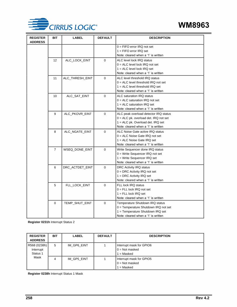
WM8963
258 Rev 4.2
REGISTER
ADDRESS
BIT LABEL DEFAULT DESCRIPTION
0 = FIFO error IRQ not set
1 = FIFO error IRQ set
Note: cleared when a ‘1’ is written
12 ALC_LOCK_EINT 0 ALC level lock IRQ status
0 = ALC level lock IRQ not set
1 = ALC level lock IRQ set
Note: cleared when a ‘1’ is written
11 ALC_THRESH_EINT 0 ALC level threshold IRQ status
0 = ALC level threshold IRQ not set
1 = ALC level threshold IRQ set
Note: cleared when a ‘1’ is written
10 ALC_SAT_EINT 0 ALC saturation IRQ status
0 = ALC saturation IRQ not set
1 = ALC saturation IRQ set
Note: cleared when a ‘1’ is written
9 ALC_PKOVR_EINT 0 ALC peak overload detector IRQ status
0 = ALC pk. overload det. IRQ not set
1 = ALC pk. Overload det. IRQ set
Note: cleared when a ‘1’ is written
8 ALC_NGATE_EINT 0 ALC Noise Gate active IRQ status
0 = ALC Noise Gate IRQ not set
1 = ALC Noise Gate IRQ set
Note: cleared when a ‘1’ is written
7 WSEQ_DONE_EINT 0 Write Sequencer done IRQ status
0 = Write Sequencer IRQ not set
1 = Write Sequencer IRQ set
Note: cleared when a ‘1’ is written
6 DRC_ACTDET_EINT 0 DRC Activity IRQ status
0 = DRC Activity IRQ not set
1 = DRC Activity IRQ set
Note: cleared when a ‘1’ is written
5 FLL_LOCK_EINT 0 FLL lock IRQ status
0 = FLL lock IRQ not set
1 = FLL lock IRQ set
Note: cleared when a ‘1’ is written
0 TEMP_SHUT_EINT 0 Temperature Shutdown IRQ status
0 = Temperature Shutdown IRQ not set
1 = Temperature Shutdown IRQ set
Note: cleared when a ‘1’ is written
Register 0231h Interrupt Status 2
REGISTER
ADDRESS
BIT LABEL DEFAULT DESCRIPTION
R568 (0238h)
Interrupt
Status 1
Mask
5 IM_GP6_EINT 1 Interrupt mask for GPIO6
0 = Not masked
1 = Masked
4 IM_GP5_EINT 1 Interrupt mask for GPIO5
0 = Not masked
1 = Masked
Register 0238h Interrupt Status 1 Mask

WM8963
Rev 4.2 259
REGISTER
ADDRESS
BIT LABEL DEFAULT DESCRIPTION
R569 (0239h)
Interrupt
Status 2
Mask
15 IM_MICSCD_
EINT
1 Interrupt mask for Mic Short Circuit
0 = Not masked
1 = Masked
14 IM_MICD_EINT 1 Interrupt mask for Mic Detect
0 = Not masked
1 = Masked
13 IM_FIFOS_ERR_
EINT
1 Interrupt mask for FIFOS Error
0 = Not masked
1 = Masked
12 IM_ALC_LOCK_
EINT
1 Interrupt mask for ALC Lock
0 = Not masked
1 = Masked
11 IM_ALC_
THRESH_EINT
1 Interrupt mask for ALC Threshold
0 = Not masked
1 = Masked
10 IM_ALC_SAT_
EINT
1 Interrupt mask for ALC Saturation
0 = Not masked
1 = Masked
9 IM_ALC_
PKOVR_EINT
1 Interrupt mask for ALC Peak Detector overload
0 = Not masked
1 = Masked
8 IM_ALC_NGATE
_EINT
1 Interrupt mask for ALC Noise Gate active
0 = Not masked
1 = Masked
7 IM_WSEQ_
DONE_EINT
1 Interrupt mask for Write Sequencer done
0 = Not masked
1 = Masked
6 IM_DRC_
ACTDET_EINT
1 Interrupt mask for DRC Activity detect
0 = Not masked
1 = Masked
5 IM_FLL_LOCK_EINT 1 Interrupt mask for FLL Lock
0 = Not masked
1 = Masked
4 Reserved 1 Reserved - do not change
3 Reserved 1 Reserved - do not change
2 Reserved 1 Reserved - do not change
1 Reserved 1 Reserved - do not change
0 IM_TEMP_
SHUT_EINT
1 Interrupt mask for Temperature Shutdown
0 = Not masked
1 = Masked
Register 0239h Interrupt Status 2 Mask
REGISTER
ADDRESS
BIT LABEL DEFAULT DESCRIPTION
R576 (0240h)
Interrupt
Control
0 IRQ_POL 0 Interrupt Output polarity
0 = Active high
1 = Active low
Register 0240h Interrupt Control

WM8963
260 Rev 4.2
REGISTER
ADDRESS
BIT LABEL DEFAULT DESCRIPTION
R584 (0248h)
IRQ
Debounce
5 FLL_LOCK_DB 1 Debounce Enable on FLL Lock
0 = Disabled
1 = Enabled
4 Reserved 1 Reserved - do not change
3 Reserved 1 Reserved - do not change
2 Reserved 1 Reserved - do not change
1 Reserved 1 Reserved - do not change
0 TEMP_SHUT_DB 1 Debounce Enable on Temperature Shutdown
0 = Disabled
1 = Enabled
Register 0248h IRQ Debounce
REGISTER
ADDRESS
BIT LABEL DEFAULT DESCRIPTION
R586
(024Ah)
MICINT
Source Pol
15 MICSCD_IRQ_
POL
0 Mic Short Circuit Interrupt Polarity
0 = Active high (IRQ asserted when MICSHORT_THR is
exceeded)
1 = Active low (IRQ asserted when MICSHORT_THR not
exceeded)
14 MICD_IRQ_POL 0 Mic Detect Interrupt Polarity
0 = Active high (IRQ asserted when MICDET_THR is
exceeded)
1 = Active low (IRQ asserted when MICDET_THR not
exceeded)
Register 024Ah MICINT Source Pol
REGISTER
ADDRESS
BIT LABEL DEFAULT DESCRIPTION
R768 (0300h)
DSP2 Power
Management
0 DSP2_ENA 0 DSP2 Audio Processor Enable.
0 = Disabled
1 = Enabled
This bit must be set before any of DAC ReTune, DAC HPF,
VSS or MBC is enabled. It must remain set whenever any of
these functions is enabled.
Register 0300h DSP2 Power Management
REGISTER
ADDRESS
BIT LABEL DEFAULT DESCRIPTION
R1037
(040Dh)
DSP2_
ExecControl
5 DSP2_STOPC 0 [No description available]
4 DSP2_STOPS 0 [No description available]
3 DSP2_STOPI 0 [No description available]
2 DSP2_STOP 0 Stop the DSP2 audio processor. Writing a 1 to this bit will
cause the DSP2 processor to stop processing audio data.
1 DSP2_RUNR 0 Start the DSP2 audio processor
Writing a 1 to this bit will cause the DSP2 processor to start
processing audio data
0 DSP2_RUN 0 [No description available]
Register 040Dh DSP2_ExecControl

WM8963
Rev 4.2 261
REGISTER
ADDRESS
BIT LABEL DEFAULT DESCRIPTION
R4096
(1000h)
Write
Sequencer 0
13:0 WSEQ_ADDR0
[13:0]
00_0000_
0001_1100
Control Register Address to be written to in this sequence
step.
Register 1000h Write Sequencer 0
REGISTER
ADDRESS
BIT LABEL DEFAULT DESCRIPTION
R4097
(1001h) Write
Sequencer 1
7:0 WSEQ_DATA0 [7:0] 0000_0011 Data to be written in this sequence step. When the data width
is less than 8 bits, then one or more of the MSBs of
WSEQ_DATAn are ignored. It is recommended that unused
bits be set to 0.
Register 1001h Write Sequencer 1
REGISTER
ADDRESS
BIT LABEL DEFAULT DESCRIPTION
R4098
(1002h) Write
Sequencer 2
10:8 WSEQ_DATA_
WIDTH0 [2:0]
001 Width of the data block written in this sequence step.
000 = 1 bit
001 = 2 bits
010 = 3 bits
011 = 4 bits
100 = 5 bits
101 = 6 bits
110 = 7 bits
111 = 8 bits
3:0 WSEQ_DATA_
START0 [3:0]
0011 Bit position of the LSB of the data block written in this
sequence step.
0000 = Bit 0
…
1111 = Bit 15
Register 1002h Write Sequencer 2
REGISTER
ADDRESS
BIT LABEL DEFAULT DESCRIPTION
R4099
(1003h)
Write
Sequencer 3
8 WSEQ_EOS0 0 End of Sequence flag. This bit indicates whether the Control
Write Sequencer should stop after executing this step.
0 = Not end of sequence
1 = End of sequence (Stop the sequencer after this step).
3:0 WSEQ_DELAY0
[3:0]
0000 Time delay after executing this step.
Total time per step (including execution)
= k × (2^WSEQ_DELAY + 8)
k = 62.5µs (SAMPLE_RATE_INT_MODE = 1),
k = 68.1µs (SAMPLE_RATE_INT_MODE = 0),
Register 1003h Write Sequencer 3

WM8963
262 Rev 4.2
REGISTER
ADDRESS
BIT LABEL DEFAULT DESCRIPTION
R4100
(1004h) Write
Sequencer 4
To
R4607
(11FFh)
Write
Sequencer
511
[Write Sequencer Control Registers]
Register 1004h Write Sequencer 4 to Register 11FFh Write Sequencer 511
REGISTER
ADDRESS
BIT LABEL DEFAULT DESCRIPTION
R16386 (4002h)
RETUNEDAC_
SHARED_
COEFF_1
7 DAC_RETUNE_SCV 0 DAC ReTune Coefficient sharing
0 = Left and Right channels each use unique coefficients
1 = Both channels use the Right Channel coefficients
6:0 RETUNEDAC
_SHARED_COEFF_
23_16 [6:0]
000_0000 [No description available]
Register 4002h RETUNEDAC_SHARED_COEFF_1
REGISTER
ADDRESS
BIT LABEL DEFAULT DESCRIPTION
R16387 (4003h)
RETUNEDAC_
SHARED_
COEFF_0
15:0 RETUNEDAC_
SHARED_COEFF_
15_00 [15:0]
0000_0000_
0000_0000
[No description available]
Register 4003h RETUNEDAC_SHARED_COEFF_0
REGISTER
ADDRESS
BIT LABEL DEFAULT DESCRIPTION
R16388 (4004h)
SOUNDSTAGE_
ENABLES_1
7:0 SOUNDSTAGE_
ENABLES_23_
16 [7:0]
0000_0000 [No description available]
Register 4004h SOUNDSTAGE_ENABLES_1
REGISTER
ADDRESS
BIT LABEL DEFAULT DESCRIPTION
R16389 (4005h)
SOUNDSTAGE_
ENABLES_0
15:6 SOUNDSTAGE_
ENABLES_15_06
[9:0]
00_0000_000
0
[No description available]
4 RTN_DAC_ENA 0 DAC ReTune enable
0 = Disabled
1 = Enabled
3 MBC_ENA 0 MBC Enable
0 = Disabled
1 = Enabled

WM8963
Rev 4.2 263
REGISTER
ADDRESS
BIT LABEL DEFAULT DESCRIPTION
2 HPF2_ENA 0 High-Pass Filter (HPF2) enable
0 = Disabled
1 = Enabled
1 HPF1_ENA 0 High-Pass Filter (HPF1) enable
0 = Disabled
1 = Enabled
0 VSS_ENA 0 Virtual Surround Sound (VSS) enable
0 = Disabled
1 = Enabled
Register 4005h SOUNDSTAGE_ENABLES_0
REGISTER
ADDRESS
BIT LABEL DEFAULT DESCRIPTION
R16896 (4200h)
MBC Band 1 K
(1)
To
R16955 (423Bh)
MBC RMS
Limit (2)
[MBC Control Registers]
Register 4200h MBC Band 1 K (1) to Register 423Bh MBC RMS Limit (2)
REGISTER
ADDRESS
BIT LABEL DEFAULT DESCRIPTION
R17408 (4400h)
HPF_C_1
To
R17409 (4401h)
HPF_C_0
[DAC High Pass Filter Control Registers]
Register 4400h HPF_C_1 to Register 4401h HPF_C_0
REGISTER
ADDRESS
BIT LABEL DEFAULT DESCRIPTION
R17920 (4600h)
DACL_RETUNE
_C1_1
To
R19007 (4A3Fh)
DACR_RETUNE
_
C32_0
[DAC ReTune Control Registers]
Register 4600h DACL_RETUNE_C1_1 to Register 4A3Fh DACR_RETUNE_C32_0

WM8963
264 Rev 4.2
REGISTER
ADDRESS
BIT LABEL DEFAULT DESCRIPTION
R19456 (4C00h)
VSS_XHD2_1
To
R19603
(4C93h)
VSS_XTS32_0
[VSS Control Registers]
Register 4600h DACL_RETUNE_C1_1 to Register 4C93h VSS_XTS32_0

WM8963
Rev 4.2 265
DIGITAL FILTER CHARACTERISTICS
PARAMETER TEST CONDITIONS MIN TYP MAX UNIT
ADC Filter
Passband 0.454 fs
-3dB 0.5 fs
Passband Ripple f < 0.454 fs +/- 0.05 dB
Stopband 0.546 fs
Stopband Attenuation f > 0.546 fs 60 dB
DAC Normal Filter
Passband 0.454 fs
-6dB 0.5 fs
Passband Ripple f < 0.454 fs +/- 0.05 dB
Stopband 0.546 fs
Stopband Attenuation 0.546 fs < f < 30 fs 50 dB
DAC Sloping Stopband Filter
Passband 0.454 fs
-9dB 0.5 fs
Passband Ripple f < 0.25 fs +/- 0.05 dB
0.25 fs < f < 0.454 fs +/- 1
Stopband 1 0.546 fs 0.7 fs
Stopband 1 Attenuation f > 0.546 fs 60 dB
Stopband 2 0.7 fs 1.4 fs
Stopband 2 Attenuation f > 0.7 fs 85 dB
Stopband 3 1.4 fs
Stopband 3 Attenuation 1.4 fs < f < 30 fs 53 dB
DAC FILTERS ADC FILTERS
Mode Group Delay Mode Group Delay
Normal 16.5 / fs Normal 15 / fs
Sloping Stopband 18 / fs
TERMINOLOGY
1. Stop Band Attenuation (dB) – the degree to which the frequency spectrum is attenuated (outside audio band)
2. Pass-band Ripple – any variation of the frequency response in the pass-band region

WM8963
266 Rev 4.2
DAC FILTER RESPONSES
This series of plots shows the filter response for the entire DAC channel for different signal rates. The
full path, has a nominal gain of 3.01dB (1V input, 1.414V output), this means that the highest nodes in
the 48kHz case are at 47.5dB (rather than below the 50dB specification).
SAMPLE RATE
(KHZ)
SLOPING STOP-BAND MCLK RECOMMENDED RATE FOR
DAC ONLY PLAYBACK (CODEC
MODE) (HZ)
8 Yes 3072000 (3072000)
11.025 Yes 2822400 (2822400)
12 Yes 3072000 (3072000)
16 Yes 2048000 (6144000)
22.05 Yes 2822400 (5644800)
24 Yes 3072000 (6144000)
32 No 2048000 (8192000)
44.1 No 2822400 (11289600)
48 No 3072000 (12288000)
Table 127 Recommended Filter Configurations for Supported Sample Rates
Figure 74 DAC Filter Response 8k Sampling Rate Figure 75 DAC Filter Response for 11.025k Sample Rate
Figure 76 DAC Filter Response for 12k Sample Rate Figure 77 DAC Filter Response for 16k Sample Rate

WM8963
Rev 4.2 267
Figure 78 DAC Filter Response 22.05k Sample Rate Figure 79 DAC Playback Filter Response for 24k Sample
Rate
Figure 80 DAC Playback Filter Response for 32k Sample
Rate
Figure 81 DAC Playback Filter Response for 44.1k Sample
Rate
Figure 82 DAC Playback Filter Response for 48k Sample
Rate
Figure 83 DAC Playback Filter Passband Ripple for 44.1k
Sample Rate (MCLK=11.2896MHZ)

WM8963
268 Rev 4.2
ADC FILTER RESPONSES
Figure 84 ADC Digital Filter Frequency Response (128OSR)
Figure 85 ADC Digital Filter Passband Ripple (128OSR)

WM8963
Rev 4.2 269
ADC HIGH PASS FILTER RESPONSES
Figure 86 ADC Digital High Pass Filter Frequency Response (48kHz, Hi-Fi Mode, ADC_HPF_CUT[1:0]=00)
hpf_response.res MAGNITUDE(dB) hpf_response2.res MAGNITUDE(dB)
hpf_response2.res#1 MAGNITUDE(dB)
2 5.0248 12.624 31.716 79.683 200.19 502.96 1.2636k 3.1747k 7.9761k 20.039k
-83.352
-75.017
-66.682
-58.347
-50.012
-41.677
-33.342
-25.007
-16.672
-8.3373
-2.3338m
Figure 87 ADC Digital High Pass Filter Ripple (48kHz, Voice Mode, ADC_HPF_CUT=01, 10 and 11)

WM8963
270 Rev 4.2
DE-EMPHASIS FILTER RESPONSES
MAGNITUDE(dB)
-10
-9
-8
-7
-6
-5
-4
-3
-2
-1
0
0 5000 10000 15000 20000
Frequency (Hz)
MAGNITUDE(dB)
-0.15
-0.1
-0.05
0
0.05
0.1
0.15
0.2
0.25
0.3
0 2000 4000 6000 8000 10000 12000 14000 16000 18000
Frequency (Hz)
Figure 88 De-Emphasis Digital Filter Response (32kHz) Figure 89 De-Emphasis Error (32kHz)
MAGNITUDE(dB)
-10
-9
-8
-7
-6
-5
-4
-3
-2
-1
0
0 5000 10000 15000 20000 25000
Frequency (Hz)
MAGNITUDE(dB)
-0.1
-0.05
0
0.05
0.1
0.15
0.2
0 5000 10000 15000 20000 25000
Frequency (Hz)
Figure 90 De-Emphasis Digital Filter Response (44.1kHz) Figure 91 De-Emphasis Error (44.1kHz)
MAGNITUDE(dB)
-12
-10
-8
-6
-4
-2
0
0 5000 10000 15000 20000 25000 30000
Frequency (Hz)
MAGNITUDE(dB)
-0.15
-0.1
-0.05
0
0.05
0.1
0.15
0 5000 10000 15000 20000 25000 30000
Frequency (Hz)
Figure 92 De-Emphasis Digital Filter Response (48kHz) Figure 93 De-Emphasis Error (48kHz)

WM8963
Rev 4.2 271
APPLICATIONS INFORMATION
RECOMMENDED EXTERNAL COMPONENTS
ANALOGUE INPUT PATHS
The WM8963 provides up to 8 analogue audio input paths. Each of these inputs is referenced to the
internal DC reference, VMID. A DC blocking capacitor is required for each analogue input pin used in
the target application. The choice of capacitor is determined by the filter that is formed between that
capacitor and the impedance of the input pin. The circuit is illustrated in Figure 94.
InputC
Fc = high pass 3dB cut-off frequency
Fc = 1
2 RCp
To input
boost mixer
+
-
PGA
VMID
eg. 1F
R
Figure 94 Audio Input Path DC Blocking Capacitor
In accordance with the WM8963 input pin resistance, it is recommended that a 1F capacitance will
give good results in most cases. Note that the input impedance, R, changes with the PGA gain
setting, as described in the “Electrical Characteristics”.
A single capacitor is required for line or microphone input connection. Tantalum electrolytic capacitors
are particularly suitable as they offer high stability in a small package size.
Ceramic equivalents are a cost effective alternative to the superior tantalum packages, but care must
be taken to ensure the desired capacitance is maintained at the AVDD operating voltage. Also,
ceramic capacitors may show microphonic effects, where vibrations and mechanical conditions give
rise to electrical signals. This is particularly problematic for microphone input paths where a large
signal gain is required.
The external connections for electret condenser microphones, incorporating the WM8963 microphone
bias circuit, are shown later in the “Microphone Bias Circuit” section below.
MICROPHONE BIAS CIRCUIT
The WM8963 is designed to interface easily with analogue microphones. An electret condenser
microphone (ECM) requires a bias current; this can be provided by the MICBIAS output on the
WM8963.
An electret condenser microphone may be connected in single-ended configuration, as illustrated in
Figure 95.
A decoupling capacitor is required on the MICBIAS output. A suitable capacitor must be connected
whenever the MICBIAS output is enabled.
A current-limiting resistor is also required for the ECM; the resistance should be chosen according to
the minimum operating impedance of the microphone and MICBIAS voltage so that the maximum bias
current of the WM8963 is not exceeded.
A 2.2k current-limiting resistor is recommended; this provides compatibility with a wide range of
microphone components.
Note that the MICBIAS output can also be used to power an analogue silicon microphone. In this
case, the MICBIAS connects directly to the VDD pin of the microphone - a current-limiting resistor is
not required in this case.

WM8963
272 Rev 4.2
MIC To input
boost mixer+
-
PGA
VMID
IN1L, IN4L,
IN1R, IN4R
MICBIAS
2.2k
1F
Figure 95 Single Ended Microphone Connection
Additional filtering of the MICBIAS output, to reduce noise and interference, may be implemented
using the configuration illustrated in Figure 96.
MIC To input
boost mixer+
-
PGA
VMID
IN1L, IN4L,
IN1R, IN4R
MICBIAS
1k
22F
1.2k
Figure 96 Microphone Connection, with MICBIAS Filter Components

WM8963
Rev 4.2 273
INTERNAL LDO FOR MICBIAS CIRCUIT
The WM8963 provides an internal LDO regulator, which can be used to generate a suitable MICVDD
supply for the MICBIAS generator. The LDO supply is provided via the LDOVDD pin. The LDO input is
suitable for direct connection to a battery.
When the LDO is used to generate the MICVDD supply, there should be no external connections to
the MICVDD pin. The recommended connections are illustrated in Figure 97.
The LDOVDD supply voltage must be at least 250mV higher than the desired MICVDD output voltage.
MICBIASMICBIAS_ENA
MICBIAS_EVR
MICBIAS_LVL
LDOVDD
LDO_VOUT_SEL
LDO_OUT_FLT
LDO_ENA
MICVDD
LDO
1F
4.7F
LDO_ENA=1
(no connection)
(2.7V to 5.5V)
Figure 97 LDO Connection for MICBIAS
When the LDO is not used, then the MICVDD and LDOVDD pins should be tied together, and
connected to a suitable MICVDD supply. The recommended connections are illustrated in Figure 98.
MICBIASMICBIAS_ENA
MICBIAS_EVR
MICBIAS_LVL
LDOVDD
LDO_VOUT_SEL
LDO_OUT_FLT
LDO_ENA
MICVDD
LDO
1F
4.7F
LDO_ENA=0
LDO_OUT_FLT=1
(1.7V to 3.6V)
Figure 98 LDO Connections (LDO not used)

WM8963
274 Rev 4.2
CHARGE PUMP COMPONENTS
The WM8963 incorporates a Charge Pump circuit, which generates the CPVOUTP and CPVOUTN
supply rails for the ground-referenced headphone drivers.
Decoupling capacitors are required on each of the Charge Pump outputs. A fly-back capacitor is also
required. The recommended Charge Pump capacitors for WM8963 are detailed below in Table 128.
DESCRIPTION CAPACITOR
CPVOUTP decoupling Required capacitance is 2.0F at 2V.
Suitable component typically 4.7F.
CPVOUTN decoupling Required capacitance is 2.0F at 2V.
Suitable component typically 4.7F.
Charge Pump fly-back
(connect between CPCA and CPCB)
Required capacitance is 1.0F at 2V.
Suitable component typically 2.2F.
Table 128 Charge Pump External Capacitors
Ceramic capacitors are recommended for these Charge Pump requirements. Note that, due to the
wide tolerance of many types of ceramic capacitors, care must be taken to ensure that the selected
components provide the required capacitance across the required temperature and voltage ranges in
the intended application. Ceramic capacitors with X5R dielectric are recommended.
The positioning of the Charge Pump capacitors is important, particularly the fly-back capacitors.
These capacitors should be placed as close as possible to the WM8963.

WM8963
Rev 4.2 275
RECOMMENDED EXTERNAL COMPONENTS DIAGRAM
WM8963
SPKVDD1
SPKGND2
LDOVDD
SPKVDD2
VMIDC
HPOUT1L
HPOUTFB*
HPOUT1R
SPKOUTLN
SPKOUTRP
SPKOUTRN
SPKOUTLP
CPCA
CPVOUTP
CPVOUTN
CPCB
2.2F
2.2F 2.2F
Loudspeaker
4.7F
Headset
4.7F4.7F2.2F0.1F
0.1F 0.1F
Loudspeaker
CPVDD
0.1F
(Note: HPOUTFB ground
connection close to headset jack)
4.7F
Note that the optimum input capacitance will
vary according to the required frequency
response and the applicable input impedance.
2020
MICBIAS1.0F
HPOUT2L
HPOUTFB*
HPOUT2R Headset
0.1F 0.1F
(Note: HPOUTFB ground
connection close to headset jack)2020
AGND
SPKGND1
CPGND
DGND
DCVDD
DBVDD
SP
KV
DD
1
LD
OV
DD
SP
KV
DD
2
CP
VD
D
DB
VD
D
DC
VD
D
* The HPOUTFB pin is common to
HPOUT1 and HPOUT2 outputs
4.7F
AVDD
AV
DD
MICVDD Note: No connection to MICVDD when LDO is enabled.
MICVDD should be connected to LDOVDD when LDO is not used.
MCLK/XTI
XTOCrystal Oscillator
24MHz
SDA
SCLKControl Interface
CIFMODE
CS/GPIO6
DACDAT
LRCLK
BCLK
ADCDAT
Audio Interface
OSCENA/GPIO5
CLKOUT2/GPIO2
CLKOUT5
GPIO /
External Clocking
Note that GPIO5 must be in a defined
state (logic ‘0’ or logic ‘1’) during
start-up; it must not be left floating.
IN1L
IN2R
IN2L
IN1R
1F
1F
1F
1F
Analogue Audio
(Mic / Line) Inputs
IN3L
IN4R
IN4L
IN3R
1F
1F
1F
1F
Figure 99 WM8963 Recommended External Components

WM8963
276 Rev 4.2
Notes:
1. Power Supply Decoupling Capacitors
X5R ceramic capacitor is recommended for the power supply decoupling capacitors.
The decoupling capacitors on VMIDC, MICBIAS, CPVOUTP and CPVOUTN should be as close to the WM8963 as possible.
2. Charge Pump Capacitors
Specific recommendations for Charge Pump capacitors are provided in Table 129. Note that two different recommendations are
provided for CPVOUTP and CPVOUTN; either of these components is suitable, depending upon size requirements and availability.
The positioning of the flyback capacitor is very important - this should be as close to the WM8963 as possible.
It is important to select a suitable capacitor type for the Charge Pump. Note that the capacitance may vary with DC voltage; care is
required to ensure that required capacitance is achieved at the applicable operating voltage, as specified in Figure 99. The capacitor
datasheet should be consulted for this information.
COMPONENT REQUIRED
CAPACITANCE
VALUE PART NUMBER VOLTAGE TYPE SIZE
Charge Pump
Flyback
(CPCA to CPCB)
1F at 2VDC 2.2F Kemet C0402C225M9PAC 6.3v X5R 0402
CPVOUTN
decoupling,
CPVOUTP
decoupling
2F at 2VDC
2.2F MuRata GRM188R61A225KE34D 10v X5R 0603
4.7F MuRata GRM155R60J475M_EIA 6.3v X5R 0402
Table 129 Charge Pump Capacitors
3. Zobel Networks
The Zobel network shown in Figure 99 is required on HPOUT1L, HPOUT1R, HPOUT2L and HPOUT2R whenever that output is
enabled. Stability of these ground-referenced outputs across all process corners cannot be guaranteed without the Zobel network
components. (Note that, if any ground-referenced output pin is not required, the Zobel network components can be omitted from the
output pin, and the pin can be left floating.) The Zobel network requirement is detailed further in the applications note WAN_0212
“Class W Headphone Impedance Compensation”.
Zobel networks should be positioned reasonably close to the WM8963.
4. AGND Connections
The AGND connections must be tied together as close as possible to the WM8963.

WM8963
Rev 4.2 277
PCB LAYOUT CONSIDERATIONS
Poor PCB layout will degrade the performance and be a contributory factor in EMI, ground bounce
and resistive voltage losses. All external components should be placed as close to the WM8963
device as possible, with current loop areas kept as small as possible.
The following layout priorities should be observed. (All these components should be as close to the
WM8963 as possible; item 1. is the highest priority).
1. Charge pump capacitors
2. AVDD, DCVDD, DBVDD decoupling
3. VMIDC, MICBIAS decoupling
4. Other decoupling
5. Zobel network components

WM8963
278 Rev 4.2
MIC DETECTION SEQUENCE USING MICBIAS CURRENT
This section details an example sequence which summarises how the host processor can configure
and detect the events supported by the MICBIAS current detect function.
Mic insertion/removal
Hook switch press/release
Figure 100 shows an example of how the MICBIAS current flow varies versus time, during mic
insertion and hook switch events. The Y axis is annotated with the Mic detection thresholds, and the X
axis is annotated with the stages of an example sequence as detailed in Table 130, to illustrate how
the host processor can implement mic insertion and hook switch detection.
The sequence assumes that the microphone insertion and hook switch detection functions are
monitored by polling the interrupt flags using the control interface. Note that the maximum mechanical
bounce times for mic insertion and removal must be fully understood by the software programmer.
Time
Mic Hook Switch Threshold
Mic Detect Interrupt
MIC
BIA
S C
urr
en
t
(1) (2) (4) (5) (6) (7) (8) (9)
TDETTDET
Mic Detect Threshold
Hysteresis
(3) (10)
TSHORT
TSHORT
Mic Detect Interrupt Polarity
Mic Short Interrupt
Mic Short Interrupt Polarity
MICD_EINT
MICD_IRQ_POL
MICSCD_EINT
MICSCD_IRQ_POL
HOST
PROCESSOR
Read the Mic detect interrupt
flag. If high, can then set
MICD_IRQ_POL to 1,
but only if mechanical bounce
phase has finished. Clear
MICD_EINT by writing ‘1’.
Read the Hook switch interrupt flag.
If high, can immediately set
MICSCD_IRQ_POL to 1. Clear
MICSCD_EINT by writing ‘1’.
Read the Hook switch interrupt flag. If high, can
immediately clear MICSCD_IRQ_POL to 0.
Clear MICSCD_EINT by writing ‘1’.
Read the Mic detect interrupt flag. If high, can
then clear MICD_IRQ_POL to 0, but only if
mechanical bounce phase has finished. Clear
MICD_EINT by writing ‘1’.
Step
(1) (2) (4) (5) (6) (7) (8) (9)(3) (10)Step
Example plot of MICBIAS Current versus time
Mic inserted
Hook switch
pressed
Figure 100 Mic Insert and Hook Switch Detect: Example MICBIAS Current Plot

WM8963
Rev 4.2 279
STEP DETAILS
1 Mic not inserted. To detect mic insertion, Host processor must initialise interrupts and clear MICD_IRQ_POL = 0. At
every step, the host processor should poll the interrupt status register.
Note that Mic Insertion de-bounce circuitry is automatically enabled.
2 Mechanical bounce of jack socket during Mic insertion. Host processor may already detect a mic insertion interrupt
(MICD_EINT) during this step. Once detected, the host processor can set MICD_IRQ_POL = 1 and then clear the
interrupt, unless mechanical bounce can last longer than the shortest possible TDET, in which case the host processor
should wait until step 3.
3 Mic fully inserted. If not already set, the host processor must now set MICD_IRQ_POL = 1. If not already cleared, the
host processor must now clear the MICD_EINT interrupt. To detect Hook switch press, the host processor must clear
MICSCD_IRQ_POL = 0. At this step, the diagram shows no AC current swing, due to a very low ambient noise level.
4 Mic fully inserted. Diagram shows AC current swing due to high levels of background noise (such as wind).
5 Mechanical bounce during hook switch press. The hook switch interrupt is unlikely to be set during this step, because 10
successive samples of the MICBIAS current exceeding the hook switch threshold have not yet been sampled.
Note that Hook Switch de-bounce circuitry is automatically enabled.
6 Hook switch is fully pressed down. After TSHORT, 10 successive samples of the MICBIAS current exceeding the hook
switch threshold have been detected, hence a hook switch interrupt (MISCD_EINT) will be generated. Once detected,
the host processor can immediately set MICSCD_IRQ_POL = 1 and then clear the MICSCD_EINT interrupt.
7 Mechanical bounce during hook switch release. The hook switch interrupt is unlikely to be set during this step, because
10 successive samples of the MICBIAS current lower than the hook switch threshold have not yet been sampled.
8 Hook switch fully released. After TSHORT, 10 successive samples of the MICBIAS current lower than the hook switch
threshold have been detected, hence a hook switch interrupt (MICSCD_EINT) will be generated. Once detected, the host
processor can immediately clear MICSCD_IRQ_POL = 0 and then clear the MICSCD_EINT interrupt.
9 Mechanical bounce of jack socket during Mic removal. Host processor may already detect a mic removal interrupt
(MICD_EINT) during this step. Once detected, the host processor can clear MICD_IRQ_POL = 0 and then clear the
interrupt, unless mechanical bounce can last longer than the shortest possible TDET, in which case the host processor
should wait until step 10.
10 Mic fully removed. If not already cleared, the host processor must now clear MICD_IRQ_POL = 0. If not already cleared,
the host processor must now clear the MICD_EINT interrupt.
Table 130 Mic Insert and Hook Switch Detect: Example Sequence

WM8963
280 Rev 4.2
PACKAGE DIMENSIONS
B: 49 BALL W-CSP PACKAGE 3.594 X 3.984 X 0.7mm BODY, 0.50 mm BALL PITCH
A1
CORNER
TOP VIEW
E
Abbb2 X
D
5
4
DETAIL 2
DETAIL 2
A
A2
2
Baaa2 X
A1
Zbbb
Z
1
SOLDER BALL
E1
A
D1
DETAIL 1
D
C
B
G
F
E
e
e
BOTTOM VIEW
16 5 4 3 2
6
f1
f2
h
NOTES:
1. PRIMARY DATUM -Z- AND SEATING PLANE ARE DEFINED BY THE SPHERICAL CROWNS OF THE SOLDER BALLS.
2. THIS DIMENSION INCLUDES STAND-OFF HEIGHT ‘A1’ AND BACKSIDE COATING.
3. A1 CORNER IS IDENTIFIED BY INK/LASER MARK ON TOP PACKAGE.
4. BILATERAL TOLERANCE ZONE IS APPLIED TO EACH SIDE OF THE PACKAGE BODY.
5. ‘e’ REPRESENTS THE BASIC SOLDER BALL GRID PITCH.
6. THIS DRAWING IS SUBJECT TO CHANGE WITHOUT NOTICE.
7. FOLLOWS JEDEC DESIGN GUIDE MO-211-C.
D
D1
E
E1
e
3.00 BSC
3.984
0.285
3.00 BSC
0.50 BSC
3.594
Dimensions (mm)Symbols
MIN NOM MAX NOTE
A 0.700
A2 0.443 0.456 0.469
5
f1
0.7390.661
h 0.314
7
DM112.A
0.480f2
3.569 3.619
3.959 4.009
A1 0.207 0.244 0.281
0.264 0.364
aaa
bbb
ccc
ddd
0.025
0.060
0.030
0.015
A
BZddd M A B
Zccc

WM8963
Rev 4.2 281
IMPORTANT NOTICE
Contacting Cirrus Logic Support For all product questions and inquiries, contact a Cirrus Logic Sales Representative.
To find one nearest you, go to www.cirrus.com.
The products and services of Cirrus Logic International (UK) Limited; Cirrus Logic, Inc.; and other companies in the Cirrus Logic
group (collectively either “Cirrus Logic” or “Cirrus”) are sold subject to Cirrus Logic’s terms and conditions of sale supplied at the
time of order acknowledgment, including those pertaining to warranty, indemnification, and limitation of liability. Software is provided
pursuant to applicable license terms. Cirrus Logic reserves the right to make changes to its products and specifications or to
discontinue any product or service without notice. Customers should therefore obtain the latest version of relevant information from
Cirrus Logic to verify that the information is current and complete. Testing and other quality control techniques are utilized to the
extent Cirrus Logic deems necessary. Specific testing of all parameters of each device is not necessarily performed. In order to
minimize risks associated with customer applications, the customer must use adequate design and operating safeguards to
minimize inherent or procedural hazards. Cirrus Logic is not liable for applications assistance or customer product design. The
customer is solely responsible for its selection and use of Cirrus Logic products. Use of Cirrus Logic products may entail a choice
between many different modes of operation, some or all of which may require action by the user, and some or all of which may be
optional. Nothing in these materials should be interpreted as instructions or suggestions to choose one mode over another.
Likewise, description of a single mode should not be interpreted as a suggestion that other modes should not be used or that they
would not be suitable for operation. Features and operations described herein are for illustrative purposes only.
CERTAIN APPLICATIONS USING SEMICONDUCTOR PRODUCTS MAY INVOLVE POTENTIAL RISKS OF DEATH, PERSONAL
INJURY, OR SEVERE PROPERTY OR ENVIRONMENTAL DAMAGE (“CRITICAL APPLICATIONS”). CIRRUS LOGIC PRODUCTS
ARE NOT DESIGNED, AUTHORIZED OR WARRANTED FOR USE IN PRODUCTS SURGICALLY IMPLANTED INTO THE BODY,
AUTOMOTIVE SAFETY OR SECURITY DEVICES, NUCLEAR SYSTEMS, LIFE SUPPORT PRODUCTS OR OTHER CRITICAL
APPLICATIONS. INCLUSION OF CIRRUS LOGIC PRODUCTS IN SUCH APPLICATIONS IS UNDERSTOOD TO BE FULLY AT
THE CUSTOMER’S RISK AND CIRRUS LOGIC DISCLAIMS AND MAKES NO WARRANTY, EXPRESS, STATUTORY OR
IMPLIED, INCLUDING THE IMPLIED WARRANTIES OF MERCHANTABILITY AND FITNESS FOR PARTICULAR PURPOSE,
WITH REGARD TO ANY CIRRUS LOGIC PRODUCT THAT IS USED IN SUCH A MANNER. IF THE CUSTOMER OR
CUSTOMER’S CUSTOMER USES OR PERMITS THE USE OF CIRRUS LOGIC PRODUCTS IN CRITICAL APPLICATIONS,
CUSTOMER AGREES, BY SUCH USE, TO FULLY INDEMNIFY CIRRUS LOGIC, ITS OFFICERS, DIRECTORS, EMPLOYEES,
DISTRIBUTORS AND OTHER AGENTS FROM ANY AND ALL LIABILITY, INCLUDING ATTORNEYS’ FEES AND COSTS, THAT
MAY RESULT FROM OR ARISE IN CONNECTION WITH THESE USES.
This document is the property of Cirrus Logic and by furnishing this information, Cirrus Logic grants no license, express or implied,
under any patents, mask work rights, copyrights, trademarks, trade secrets or other intellectual property rights. Any provision or
publication of any third party’s products or services does not constitute Cirrus Logic’s approval, license, warranty or endorsement
thereof. Cirrus Logic gives consent for copies to be made of the information contained herein only for use within your organization
with respect to Cirrus Logic integrated circuits or other products of Cirrus Logic, and only if the reproduction is without alteration and
is accompanied by all associated copyright, proprietary and other notices and conditions (including this notice). This consent does
not extend to other copying such as copying for general distribution, advertising or promotional purposes, or for creating any work
for resale. This document and its information is provided “AS IS” without warranty of any kind (express or implied). All statutory
warranties and conditions are excluded to the fullest extent possible. No responsibility is assumed by Cirrus Logic for the use of
information herein, including use of this information as the basis for manufacture or sale of any items, or for infringement of patents
or other rights of third parties. Cirrus Logic, Cirrus, the Cirrus Logic logo design, SoundClear, WISCE, ReTune, and SilentSwitch are
among the trademarks of Cirrus Logic. Other brand and product names may be trademarks or service marks of their respective
owners.
Copyright © 2013–2016 Cirrus Logic, Inc. All rights reserved.
SPI is a trademark of Motorola.

WM8963
282 Rev 4.2
REVISION HISTORY
DATE REV DESCRIPTION OF CHANGES PAGE CHANGED BY
23/05/13 2.0 First Release PH
28/08/13 3.0 Recommended operating conditions updated regarding AVDD, DCVDD,
CPVDD constraints when device is powered down.
LDO requirements updated, to ensure MICVDD is not left floating.
Electrical Characteristics updated.
Input mixer to Speaker mixer gain controls updated.
PH
20/02/14 4.0 Minimum DCVDD for restricted clocking configurations changed to 1.7V.
Maximum current consumption figures updated.
Electrical Characteristics updated.
Amendments to recommended DSP control sequences.
Additional requirements for writing 24-bit DSP configuration registers.
Digital Core block diagram updated, consistent with ADC Enhancements
functions (Second Order Filter is included within ADC Enhancements).
PH
22/07/14 4.1 DF1 filter as input to DRC is deleted 67, 79, 80, 96 PH
13/01/16 4.1 Minimum MICVDD requirements amended 18, 36 PH
05/08/16 4.2 Correction to OSC_TRIM_XTI and OSC_TRIM_XTO field definitions 159 PH