description pin assignments - diodes incorporated€¢ sot25: available in “green” molding...
TRANSCRIPT
AL8805 Document number: DS35030 Rev. 4 - 2
1 of 16 www.diodes.com
July 2012© Diodes Incorporated
AL8805
HIGH EFFICIENCY 36V 1A BUCK LED DRIVER
Description The AL8805 is a step-down DC/DC converter designed to drive LEDs with a constant current. The device can drive up to 8 LEDs, depending on the forward voltage of the LEDs, in series from a voltage source of 6V to 36V. Series connection of the LEDs provides identical LED currents resulting in uniform brightness and eliminating the need for ballast resistors. The AL8805 switches at frequency up to 1MHz. This allows the use of small size external components, hence minimizing the PCB area needed.
Maximum output current of AL8805 is set via an external resistor connected between the VIN and SET input pins. Dimming is achieved by applying either a DC voltage or a PWM signal at the CTRL input pin. An input voltage of 0.4V or lower at CTRL switches off the output MOSFET simplifying PWM dimming.
Features • LED Driving Current up to 1A • Better than 5% Accuracy • High Efficiency up to 98% • Operating Input Voltage from 6V to 36V • High Switching Frequency up to 1MHz • PWM/DC Input for Dimming Control • Built-In Output Open-Circuit Protection • SOT25: Available in “Green” Molding Compound (No Br,Sb) with
lead Free Finish/ RoHS Compliant Totally Lead-Free & Fully RoHS Compliant (Notes 1 & 2) Halogen and Antimony Free. “Green” Device (Note 3)
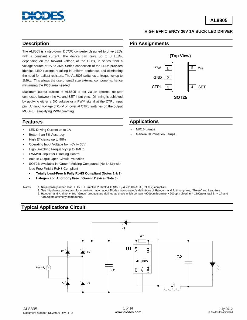
Pin Assignments
4 SET
5 VINSW 1
CTRL 3
GND 2
(Top View)
SOT25
Applications • MR16 Lamps • General Illumination Lamps
Notes: 1. No purposely added lead. Fully EU Directive 2002/95/EC (RoHS) & 2011/65/EU (RoHS 2) compliant. 2. See http://www.diodes.com for more information about Diodes Incorporated’s definitions of Halogen- and Antimony-free, "Green" and Lead-free.
3. Halogen- and Antimony-free "Green” products are defined as those which contain <900ppm bromine, <900ppm chlorine (<1500ppm total Br + Cl) and <1000ppm antimony compounds.
Typical Applications Circuit

AL8805 Document number: DS35030 Rev. 4 - 2
2 of 16 www.diodes.com
July 2012© Diodes Incorporated
AL8805
Pin Descriptions
Pin Number Pin Name Function
1 SW Switch Pin. Connect inductor/freewheeling diode here, minimizing track length at this pin to reduce EMI.
2 GND GND Pin
3 CTRL
Dimming and On/Off Control Input. • Leave floating for normal operation.
(VCTRL = VREF = 2.5V giving nominal average output current IOUTnom = 0.1/RS) • Drive to voltage below 0.4V to turn off output current • Drive with DC voltage (0.5V < VCTRL < 2.5V) to adjust output current from 20% to 100% of IOUTnom • A PWM signal (low level ≤ 0.4V and high level > 2.6; transition times less than 1us) allows the output
current to be adjusted below the level set by the resistor connected to SET input pin.
4 SET Set Nominal Output Current Pin. Configure the output current of the device.
5 VIN Input Supply Pin. Must be locally decoupled to GND with > 2.2µF X7R ceramic capacitor – see applications section for more information.
Absolute Maximum Ratings (@TA = +25°C, unless otherwise specified.)
Symbol Parameter Ratings Unit
ESD HBM Human Body Model ESD Protection 2.5 kV
ESD MM Machine Model ESD Protection 200 V
VIN Continuous VIN Pin Voltage Relative to GND -0.3 to 40 V
VSET SET Pin Voltage Relative to VIN Pin -5 to +0.3 V
VSW SW Voltage Relative to GND -0.3 to 40 V
VCTRL CTRL Pin Input Voltage -0.3 to 6 V
ISW-DC DC or RMS Switch current 1.25 A
ISW-PK Peak Switch Current (<10%) 2.5 A
TJ Junction Temperature 150 °C
TLEAD Lead Temperature Soldering 300 °C
TST Storage Temperature Range -65 to +150 °C Caution: Stresses greater than the 'Absolute Maximum Ratings' specified above, may cause permanent damage to the device. These are stress ratings only;
functional operation of the device at these or any other conditions exceeding those indicated in this specification is not implied. Device reliability may be affected by exposure to absolute maximum rating conditions for extended periods of time.
Semiconductor devices are ESD sensitive and may be damaged by exposure to ESD events. Suitable ESD precautions should be taken when handling and transporting these devices
Recommended Operating Conditions (@TA = +25°C, unless otherwise specified.)
Symbol Parameter Min Max Unit
VIN Operating Input Voltage relative to GND 6.0 36 V
VCTRLH Voltage High for PWM Dimming Relative to GND 2.6 5.5 V
VCTRLDC Voltage Range for 20% to 100% DC Dimming Relative to GND 0.5 2.5 V
VCTRLL Voltage Low for PWM Dimming Relative to GND 0 0.4 V
ISW Continuous Switch Current — 1 A
TJ Junction Temperature Range -40 125 °C
AL8805 Document number: DS35030 Rev. 4 - 2
3 of 16 www.diodes.com
July 2012© Diodes Incorporated
AL8805
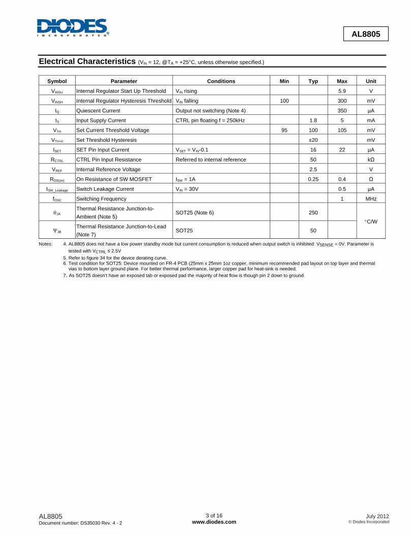
Electrical Characteristics (VIN = 12, @TA = +25°C, unless otherwise specified.)
Symbol Parameter Conditions Min Typ Max Unit
VINSU Internal Regulator Start Up Threshold VIN rising 5.9 V
VINSH Internal Regulator Hysteresis Threshold VIN falling 100 300 mV
IQ Quiescent Current Output not switching (Note 4) 350 µA
IS Input Supply Current CTRL pin floating f = 250kHz 1.8 5 mA
VTH Set Current Threshold Voltage 95 100 105 mV
VTH-H Set Threshold Hysteresis ±20 mV
ISET SET Pin Input Current VSET = VIN-0.1 16 22 µA
RCTRL CTRL Pin Input Resistance Referred to internal reference 50 kΩ
VREF Internal Reference Voltage 2.5 V
RDS(on) On Resistance of SW MOSFET ISW = 1A 0.25 0.4 Ω
ISW_Leakage Switch Leakage Current VIN = 30V 0.5 μA
fOSC Switching Frequency 1 MHz
θJA Thermal Resistance Junction-to-Ambient (Note 5)
SOT25 (Note 6) 250 °C/W
ΨJB Thermal Resistance Junction-to-Lead (Note 7)
SOT25 50
Notes: 4. AL8805 does not have a low power standby mode but current consumption is reduced when output switch is inhibited: VSENSE = 0V. Parameter is tested with VCTRL ≤ 2.5V 5. Refer to figure 34 for the device derating curve. 6. Test condition for SOT25: Device mounted on FR-4 PCB (25mm x 25mm 1oz copper, minimum recommended pad layout on top layer and thermal vias to bottom layer ground plane. For better thermal performance, larger copper pad for heat-sink is needed. 7. As SOT25 doesn’t have an exposed tab or exposed pad the majority of heat flow is though pin 2 down to ground.

AL8805 Document number: DS35030 Rev. 4 - 2
4 of 16 www.diodes.com
July 2012© Diodes Incorporated
AL8805
Typical Performance Characteristics (@TA = +25°C, unless otherwise specified.)
0
50
100
150
200
250
300
350
400
V (V)Figure 1 Supply Current (not switching) vs. Input Voltage
IN
I (µ
A)
IN
V = 0VV = VT = 25°C
CRTL
SET IN
A
0 6 12 18 24 30 360
100
200
300
400
500
600
700
800
900
0 1 2 3 4 5V (V)
Figure 2 Switching Frequency vs. VCTRL
CTRL
FRE
QU
ENC
Y (k
Hz)
V = 12V1 LEDR = 150mT = 25°C
IN
SET
A
Ω
L = 33µH
L = 68µH
L = 100µH
0
0.1
0.2
0.3
0.4
0.5
0.6
0.7
0.8
0.9
1
0 1 2 3 4 5V (V)
Figure 3 LED Current vs. VCTRL
CTRL
I (A
)LE
D
V = 12V1 LED
T = 25°C
IN
A
L = 68µH
R = 100mSET Ω
R = 150mSET Ω
R = 300mSET Ω
-60
-40
-20
0
20
40
60
80
0.0 0.5 1.0 1.5 2.0 2.5 3.0 3.5 4.0 4.5 5.0 5.5V (V)
Figure 4 I vs. VCTRL
CTRL CTRL
I (µ
A)
CTR
L
V = V = 12VT = 25°C
SET IN
A
3
2.5
2
1.5
0.5
0
V (V
)C
TRL
1
V = OpenV = V
CTRL
SET INT = 25°CA
0 3 6 9 12 18 21 24 27 30 36V (V)
Figure 5. V vs. Input Voltage(CTRL Pin Open Circuit)
IN
CTRL
15 332.48
2.49
2.50
2.51
2.52
-40 -15 10 35 60 85 110AMBIENT TEMPERATURE (°C)Figure 6 V vs. TemperatureCTRL
V (V
)C
TRL
V = OpenV = V = 12V
CTRL
SET IN

AL8805 Document number: DS35030 Rev. 4 - 2
5 of 16 www.diodes.com
July 2012© Diodes Incorporated
AL8805
Typical Performance Characteristics (cont.) (@TA = +25°C, unless otherwise specified.)
0.0
0.5
1.0
1.5
2.0
2.5
3.0
3.5
4.0
4.5
5.0
0% 20% 40% 60% 80% 100%0
0.1
0.2
0.3
0.4
0.5
0.6
0.7
0.8
0.9
1
LED
CU
RR
EN
T (A
)PWM DUTY CYCLE
Figure 7 I vs. PWM Duty CycleLED
LED
CU
RR
EN
T E
RR
OR
(%)
0
60
120
180
240
300
6 12 18 24 30 36V (V)
Figure 8 SW R vs. Input VoltageIN
DS(ON)
R (m
)D
S(O
N)
Ω
V = OpenV = VT = 25 C
CTRL
SET IN
A °
100
150
200
250
300
350
400
-40 -15 10 35 60 85 110AMBIENT TEMPERATURE (°C)
Figure 9 SW R vs. TemperatureDS(ON)
R(m
)D
S(O
N)
Ω
80
85
90
95
100
105
110
115
120
125
130
-2
0
2
4
6
8
10
12
14
16
18
TIME (µs)Figure 10 SW Output Switching Characteristics
VS
W
V(m
V)
SE
NSE
R = 150mL = 68µHV = 12V1 LED Load
SET
IN
Ω
VSW
VSENSE
ILED
VSW
VCTRL
0
0.1
0.2
0.3
0.4
0.5
0.6
0.7
0.8
0.9
1
0 50 100 150 200Time (µs)
Figure 11 PWM Dimming
0
2
4
6
8
10
12
14
16
18
20Duty Cycle = 5%
SW
ITC
H a
nd C
TRL
VOLT
AG
E (V
)
LED
CU
RR
EN
T (A
)
R = 150m , L =68µH, V = 12V, 1LED Load, T =25 CSET IN AΩ °
6 9 12 15 18 21 24 27 30INPUT VOLTAGE (V)
Figure 12 Duty Cycle vs. Input Voltage
DU
TY C
YC
LE
L = 33µHR = 150mT = 25°C2 LED
S
A
Ω
33 36

AL8805 Document number: DS35030 Rev. 4 - 2
6 of 16 www.diodes.com
July 2012© Diodes Incorporated
AL8805
Typical Performance Characteristics (cont.) (@TA = +25°C, unless otherwise specified.)
80%
82%
84%
86%
88%
90%
92%
94%
96%
98%
100%
6 9 12 15 18 21 24 27 33INPUT VOLTAGE (V)
Figure 13 Efficiency vs. Input Voltage
EFFI
CIE
NC
Y
30 36
1 LED
2 LEDs
3 LEDs
4 LEDs5 LEDs
6 LEDs 7 LEDs 8 LEDs
L = 100µHR = 150mT = 25°C
S
A
Ω
2 LEDs4 LEDs
5 LEDs 6 LEDs8 LEDs
INPUT VOLTAGE (V)Figure 14 330mA LED Current vs. Input Voltage
LED
CU
RR
EN
T (A
)
0.30
0.31
0.32
0.33
0.34
0.35
0.36
6 9 12 15 18 21 24 27 30 33 36
1 LED
3 LEDs
L = 68 HR = 300mT = 25 C
µ
°S
A
Ω
7 LEDs
0
50
100
150
200
250
300
350
INPUT VOLTAGE (V)Figure 15 Switching Frequency vs. Input Voltage
L = 100 HR = 150mT = 25 C
µ
°S
A
Ω
SW
ITC
HIN
G F
RE
QU
EN
CY
(kH
z)
6 9 12 15 18 21 24 27 30 33 36
1 LED
2 LEDs
3 LEDs 4 LEDs5 LEDs
6 LEDs7 LEDs
8 LEDs
6 9 12 15 18 21 24 27 36INPUT VOLTAGE (V)
Figure 16 670mA LED Current vs. Input Voltage
LED
CU
RR
EN
T (A
)0.720
30 33
0.710
0.700
0.690
0.680
0.670
0.660
0.650
0.640
0.630
0.620
INPUT VOLTAGE (V)Figure 17 1A LED Current vs. Input Voltage
LED
CU
RR
EN
T (A
)
0.90
0.95
1.00
1.05
1.10
6 9 12 15 18 21 24 27 30 33 36
AL8805 Document number: DS35030 Rev. 4 - 2
7 of 16 www.diodes.com
July 2012© Diodes Incorporated
AL8805
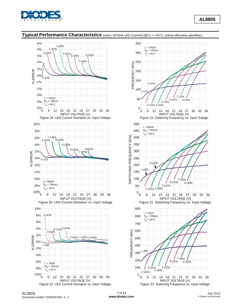
Typical Performance Characteristics (cont.) (670mA LED Current) (@TA = +25°C, unless otherwise specified.)
5%
INPUT VOLTAGE (V)Figure 18 LED Current Deviation vs. Input Voltage
% E
RR
OR
6 9 12 15 18 21 24 27 30 33 36
4%
3%
2%
1%
0%
-1%
-2%
-3%
-4%
-5% 0
50
100
150
200
250
300
350
INPUT VOLTAGE (V)Figure 19 Switching Frequency vs. Input Voltage
FRE
QU
ENC
Y (k
Hz)
L = 100 HR = 150mT = 25 C
µ
°S
A
Ω
6 9 12 15 18 21 24 27 30 33 36
1 LED
2 LEDs
3 LEDs 4 LEDs5 LEDs
6 LEDs7 LEDs
8 LEDs
INPUT VOLTAGE (V)Figure 20 LED Current Deviation vs. Input Voltage
-10%
-8%
-6%
-4%
-2%
0%
2%
4%
6%
8%
10%
% E
RR
OR
6 9 12 15 18 21 24 27 30 33 36 0
50
100
150
200
250
300
350
400
450
500
INPUT VOLTAGE (V)Figure 21 Switching Frequency vs. Input Voltage
SWIT
CH
ING
FR
EQ
UEN
CY
(kH
z)
6 9 12 15 18 21 24 27 30 33 36
-10%
-8%
-6%
-4%
-2%
0%
2%
4%
6%
8%
10%
INPUT VOLTAGE (V)Figure 22 LED Current Deviation vs. Input Voltage
% E
RR
OR
6 9 12 15 18 21 24 27 30 33 36INPUT VOLTAGE (V)
Figure 23 Switching Frequency vs. Input Voltage
0
100
200
300
400
500
600
700
800
FREQ
UE
NC
Y (k
Hz)
6 9 12 15 18 21 24 27 30 33 36
900

AL8805 Document number: DS35030 Rev. 4 - 2
8 of 16 www.diodes.com
July 2012© Diodes Incorporated
AL8805
Typical Performance Characteristics (cont.) (1A LED Current) (@TA = +25°C, unless otherwise specified.)
2 LEDs3 LEDs 5 LEDs
6 LEDs 7 LEDs
-8%
-6%
-4%
-2%
0%
2%
4%
6%
8%
10%
INPUT VOLTAGE (V)Figure 24 LED Current Deviation vs. Input Voltage
L = 100 HR = 100mT = 25 C
µ
°S
A
Ω
% E
RR
OR
-10%6 9 12 15 18 21 24 27 30 33 36
1 LED
4 LEDs
8 LEDs
0
50
100
150
200
250
INPUT VOLTAGE (V)Figure 25 Switching Frequency vs. Input Voltage
SW
ITC
HIN
G F
RE
QU
ENC
Y (k
Hz)
9 12 15 18 21 24 27 30 33 366
2 LEDs3 LEDs
-8%
-6%
-4%
-2%
0%
2%
4%
6%
8%
10%
INPUT VOLTAGE (V)Figure 26 LED Current Deviation vs. Input Voltage
L =68 HR = 100mT = 25 C
µ
°S
A
Ω
% E
RR
OR
6 9 12 15 18 21 24 27 30 33 36
8 LEDs
1 LED
4 LEDs5 LEDs
6 LEDs 7 LEDs
1 LED
2 LEDs 3 LEDs4 LEDs
6 LEDs 7 LEDs8 LEDs
0
50
100
150
200
250
300
350L = 68 HR = 100mT = 25 C
µ
°S
A
Ω
INPUT VOLTAGE (V)Figure 27 Switching Frequency vs. Input Voltage
6 9 12 15 18 21 24 27 30 33 36
5 LEDs
SWIT
CH
ING
FR
EQU
EN
CY
(kH
z)
1 LED
2 LEDs
3 LEDs
5 LEDs6 LEDs
8 LEDs
-8%
-6%
-4%
-2%
0%
2%
4%
6%
8%
10%
INPUT VOLTAGE (V)Figure 28 LED Current Deviation vs. Input Voltage
L = 33 HR = 100mT = 25 C
µ
°S
A
Ω
% E
RR
OR
-10%6 9 12 15 18 21 24 27 30 33 36
4 LEDs
0
100
200
300
400
500
600
INPUT VOLTAGE (V)Figure 29 Switching Frequency vs. Input Voltage
700
SW
ITC
HIN
G F
RE
QU
ENC
Y (k
Hz)
6 9 12 15 18 21 24 27 30 33 36

AL8805 Document number: DS35030 Rev. 4 - 2
9 of 16 www.diodes.com
July 2012© Diodes Incorporated
AL8805
Application Information AL8805 Operation In normal operation, when voltage is applied at +VIN, the AL8805 internal switch is turned on. Current starts to flow through sense resistor R1, inductor L1, and the LEDs. The current ramps up linearly, and the ramp rate is determined by the input voltage +Vin and the inductor L1.
This rising current produces a voltage ramp across R1. The internal circuit of the AL8805 senses the voltage across R1 and applies a proportional voltage to the input of the internal comparator.
When this voltage reaches an internally set upper threshold, the internal switch is turned off. The inductor current continues to flow through R1, L1, the LEDs and the schottky diode D1, and back to the supply rail, but it decays, with the rate of decay determined by the forward voltage drop of the LEDs and the schottky diode.
This decaying current produces a falling voltage at R1, which is sensed by the AL8805. A voltage proportional to the sense voltage across R1 is applied at the input of the internal comparator. When this voltage falls to the internally set lower threshold, the internal switch is turned on again. This switch-on-and-off cycle continues to provide the average LED current set by the sense resistor R1. LED Current Control The LED current is controlled by the resistor R1 in Figure 30.
Connected between VIN and SET the nominal average output current in the LED(s) is defined as:
SET
THDLED R
VI =
If the CTRL pin is driven by an external voltage (higher than 0.4V and lower than 2.5V), the average LED current is:
SET
THD
REF
CTRLLED R
VVVI =
For example for a desired LED current of 660mA and a default voltage VCTRL=2.5V the resulting resistor is:
Ω≈== m1505.25.2
66.01.0
VV
IVR
REF
CTRL
LED
THDSET
Figure 30 Typical Application Circuit
DC Dimming
The CTRL pin can be driven by an external DC voltage (VCTRL), to adjust the output current to a value below the nominal average value defined by RSET. The LED current decreases linearly with the CTRL voltage when 0.5V ≤ VCTRL ≤ 2.5V, as in Figure 2 for 4 different current levels.
When the CTRL voltage falls below the threshold, 0.4V, the output switch is turned off which allows PWM dimming.
Note that 100% brightness setting corresponds to VCTRL = VREF, nominally 2.5V. For any voltage applied on the CTRL pin that is higher than VREF, the device will not overdrive the LED current and will still set the current according to the equation VCTRL = VREF.
R1
AL8805
1
L1
VIN
SET
SW
CTRL
GND
C1
C2
D1

AL8805 Document number: DS35030 Rev. 4 - 2
10 of 16 www.diodes.com
July 2012© Diodes Incorporated
AL8805
Application Information (cont.)
PWM Dimming
LED current can be adjusted digitally, by applying a low frequency Pulse Width Modulated (PWM) logic signal to the CTRL pin to turn the device on and off. This will produce an average output current proportional to the duty cycle of the control signal. In particular, a PWM signal with a max resolution of 10bit can be applied to the CTRL pin to change the output current to a value below the nominal average value set by resistor RSET. To achieve this resolution the PWM frequency has to be lower than 500Hz, however higher dimming frequencies can be used, at the expense of dimming dynamic range and accuracy.
Typically, for a PWM frequency of 500Hz the accuracy is better than 1% for PWM ranging from 1% to 100%.
Figure 31 PWM Dimming at 500Hz
Figure 32 Low Duty Cycle PWM Dimming at 500Hz
The CTRL pin is designed to be driven by both 3.3V and 5V logic levels directly from a logic output with either an open drain output or push-pull output stage.
0
100
200
300
400
500
600
700
0% 10% 20% 30% 40% 50% 60% 70% 80% 90% 100%
PWM dimming [%]
LED
cur
rent
[mA
]
0
10
20
30
40
50
60
70
0% 1% 2% 3% 4% 5% 6% 7% 8% 9% 10%
PWM dimming [%]
LED
cur
rent
[mA
]
µC AL8805
GND
CTRLµC AL8805
GND
CTRL

AL8805 Document number: DS35030 Rev. 4 - 2
11 of 16 www.diodes.com
July 2012© Diodes Incorporated
AL8805
Application Information (cont.)
Soft Start The AL8805 does not have in-built soft-start action – this provides very fast turn off of the output the stage improving PWM dimming accuracy; nonetheless, adding an external capacitor from the CTRL pin to ground will provide a soft-start delay. This is achieved by increasing the time taken for the CTRL voltage to rise to the turn-on threshold and by slowing down the rate of rise of the control voltage at the input of the comparator. Adding a capacitor increases the time taken for the output to reach 90% of its final value, this delay is 0.1ms/nF, but will impact on the PWM dimming accuracy depending on the delay introduced.
Figure 33 Soft Start with 22nF Capacitor on CTRL Pin (VIN = 36V, ILED = 667mA, 1 LED)
Reducing Output Ripple Peak to peak ripple current in the LED(s) can be reduced, if required, by shunting a capacitor C2 across the LED(s) as shown already in the circuit schematic.
A value of 1μF will reduce the supply ripple current by a factor three (approx.). Proportionally lower ripple can be achieved with higher capacitor values. Note that the capacitor will not affect operating frequency or efficiency, but it will increase start-up delay, by reducing the rate of rise of LED voltage. By adding this capacitor the current waveform through the LED(s) changes from a triangular ramp to a more sinusoidal version without altering the mean current value. Capacitor Selection The small size of ceramic capacitors makes them ideal for AL8805 applications. X5R and X7R types are recommended because they retain their capacitance over wider voltage and temperature ranges than other types such as Z5U.
A 2.2μF input capacitor is sufficient for most intended applications of AL8805; however a 4.7μF input capacitor is suggested for input voltages approaching 36V.
AL8805 Document number: DS35030 Rev. 4 - 2
12 of 16 www.diodes.com
July 2012© Diodes Incorporated
AL8805
Application Information (cont.) Diode Selection For maximum efficiency and performance, the rectifier (D1) should be a fast low capacitance Schottky diode with low reverse leakage at the maximum operating voltage and temperature. The Schottky diode also provides better efficiency than silicon PN diodes, due to a combination of lower forward voltage and reduced recovery time.
It is important to select parts with a peak current rating above the peak coil current and a continuous current rating higher than the maximum output load current. In particular, it is recommended to have a diode voltage rating at least 15% higher than the operating voltage to ensure safe operation during the switching and a current rating at least 10% higher than the average diode current. The power rating is verified by calculating the power loss through the diode. Schottky diodes, e.g. B240 or B140, with their low forward voltage drop and fast reverse recovery, are the ideal choice for AL8805 applications. Thermal and Layout Considerations For continuous conduction mode of operation, the absolute maximum junction temperature must not be exceeded. The maximum power dissipation depends on several factors: the thermal resistance of the IC package θJA, PCB layout, airflow surrounding the IC, and difference between junction and ambient temperature. The maximum power dissipation can be calculated using the following formula:
PD(MAX) = (TJ(MAX) − TA) / θJA
where TJ(MAX) is the maximum operating junction temperature, TA is the ambient temperature, and θJA is the junction to ambient thermal resistance.
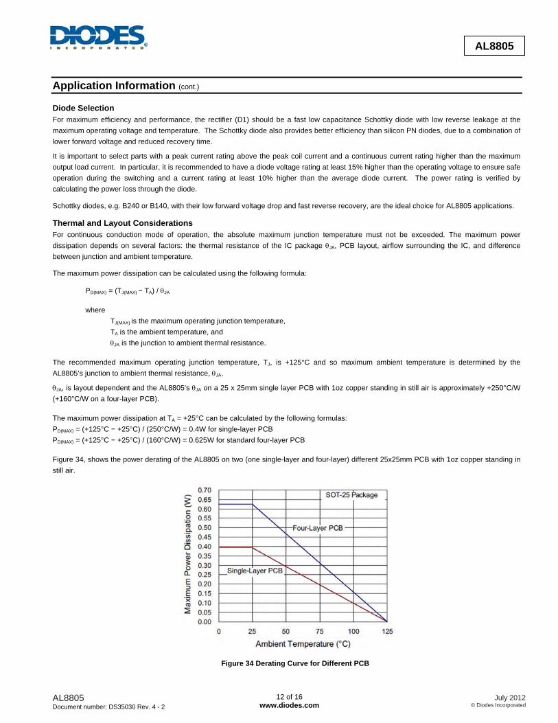
The recommended maximum operating junction temperature, TJ, is +125°C and so maximum ambient temperature is determined by the AL8805’s junction to ambient thermal resistance, θJA.
θJA, is layout dependent and the AL8805’s θJA on a 25 x 25mm single layer PCB with 1oz copper standing in still air is approximately +250°C/W (+160°C/W on a four-layer PCB). The maximum power dissipation at TA = +25°C can be calculated by the following formulas: PD(MAX) = (+125°C − +25°C) / (250°C/W) = 0.4W for single-layer PCB PD(MAX) = (+125°C − +25°C) / (160°C/W) = 0.625W for standard four-layer PCB Figure 34, shows the power derating of the AL8805 on two (one single-layer and four-layer) different 25x25mm PCB with 1oz copper standing in still air.
Figure 34 Derating Curve for Different PCB

AL8805 Document number: DS35030 Rev. 4 - 2
13 of 16 www.diodes.com
July 2012© Diodes Incorporated
AL8805
Application Information (cont.) Thermal and Layout Considerations Figure 35 gives details about the PCB layout suggestions:
1. the capacitor C1 has to be placed as close as possible to VIN 2. The sense resistor R1 has to be placed as close as possible to VIN and SET 3. The D1 anode, the SW pin and the inductor have to be placed as close as possible to avoid ringing.
Figure 35 Recommended PCB Layout
Application Example Typical application example for the AL8805 is the MR16 lamp. They typically operate from 12VDC or 12VAC, using conventional electromagnetic transformers or electronic transformers.
As a replacement in some halogen lamp applications LEDs offer a more energy efficient solution – providing no radiated heat and no Ultra Violet light.
This application example is intended to fit into the base connector space of an MR16 style LED lamp. The design has been optimized for part count and thermal performance for a single 3W LED in the Lens section.
Figure 36 MR16 Schematic
An inductor choice of 33µH with saturation current higher than 1.1A, will limit the frequency variation between 230kHz and 350kHz over the whole input voltage variation (8V to 18V), and therefore represent the best choice for an MR16 solution also taking into account the size constraint of the lamp.
The AL8805 guarantee high level of performance both with 12VAC and 12VDC power supply.
The efficiency is generally higher than 81% and current regulation is better than 0.1mA/V in for a DC input voltage in the range from 8V to 18V. In table 1 can be found the bill of material of the MR16 application example.
AL8805AL8805

AL8805 Document number: DS35030 Rev. 4 - 2
14 of 16 www.diodes.com
July 2012© Diodes Incorporated
AL8805
Application Information (cont.) In Figures 37 and 38 are displayed the top layer and the bottom layer of a typical PCB design for an MR16 solution.
Figure 37 Top Layer
Figure 38 Bottom Layer
Table1 MR16 Application Example Bill of Material
Quantity PCB Ident
Value Description Suggested
Sources 1 U1 AL8805 LED Driver IC Diodes Zetex 1 D1, DFLS240L freewheeling diode Diodes Zetex 4 D2, D3, D4, D5 SBR2A40 Input bridge Diodes Zetex
1 R1 0R15 Resistor, 0805, +/-1% <+/-300ppm Generic KOA SR732ATTDR150F
Kemet
1 C1 150uF 20V SMD tantalum Kemet D case, T491X157K020AT Kemet
0 C2 - Not fitted
1 C3 100nF > = 25V X7R 0805 Generic Kemet C0805C104K5RAC (50v) NIC NMC0805X7R104K50TRPF (50v)
Kemet NIC Components
1 C4 1uF > = 25V X7R 1206 Generic Kemet C1206105K5RAC7800 (50v) NIC NMC1206X7R105K50F (50v)
Kemet NIC Components
1 L1 33µH LPS6235 - 333MLB Coilcraft
AL8805 Document number: DS35030 Rev. 4 - 2
15 of 16 www.diodes.com
July 2012© Diodes Incorporated
AL8805
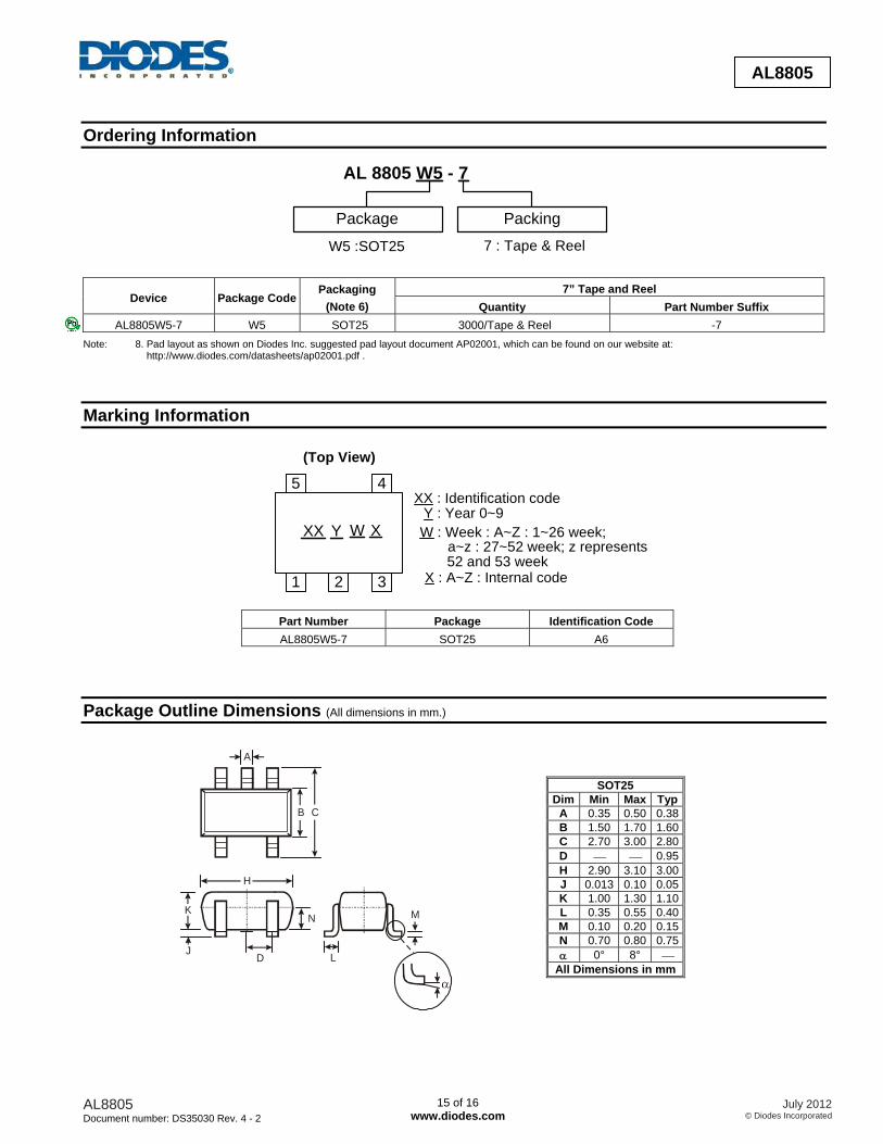
Ordering Information
AL 8805 W5 - 7
Package Packing
W5 :SOT25 7 : Tape & Reel
Device Package Code Packaging
(Note 6) 7” Tape and Reel
Quantity Part Number Suffix AL8805W5-7 W5 SOT25 3000/Tape & Reel -7
Note: 8. Pad layout as shown on Diodes Inc. suggested pad layout document AP02001, which can be found on our website at: http://www.diodes.com/datasheets/ap02001.pdf .
Marking Information
1 2 3
5 74
XX Y W X
(Top View)
XX : Identification code
W : Week : A~Z : 1~26 week;
X : A~Z : Internal code
Y : Year 0~9
a~z : 27~52 week; z represents52 and 53 week
Part Number Package Identification Code AL8805W5-7 SOT25 A6
Package Outline Dimensions (All dimensions in mm.)
SOT25 Dim Min Max Typ
A 0.35 0.50 0.38 B 1.50 1.70 1.60 C 2.70 3.00 2.80 D ⎯ ⎯ 0.95 H 2.90 3.10 3.00 J 0.013 0.10 0.05 K 1.00 1.30 1.10 L 0.35 0.55 0.40 M 0.10 0.20 0.15 N 0.70 0.80 0.75 α 0° 8° ⎯
All Dimensions in mm
A
M
J LD
B C
H
KN

AL8805 Document number: DS35030 Rev. 4 - 2
16 of 16 www.diodes.com
July 2012© Diodes Incorporated
AL8805
Suggested Pad Layout
IMPORTANT NOTICE DIODES INCORPORATED MAKES NO WARRANTY OF ANY KIND, EXPRESS OR IMPLIED, WITH REGARDS TO THIS DOCUMENT, INCLUDING, BUT NOT LIMITED TO, THE IMPLIED WARRANTIES OF MERCHANTABILITY AND FITNESS FOR A PARTICULAR PURPOSE (AND THEIR EQUIVALENTS UNDER THE LAWS OF ANY JURISDICTION). Diodes Incorporated and its subsidiaries reserve the right to make modifications, enhancements, improvements, corrections or other changes without further notice to this document and any product described herein. Diodes Incorporated does not assume any liability arising out of the application or use of this document or any product described herein; neither does Diodes Incorporated convey any license under its patent or trademark rights, nor the rights of others. Any Customer or user of this document or products described herein in such applications shall assume all risks of such use and will agree to hold Diodes Incorporated and all the companies whose products are represented on Diodes Incorporated website, harmless against all damages. Diodes Incorporated does not warrant or accept any liability whatsoever in respect of any products purchased through unauthorized sales channel. Should Customers purchase or use Diodes Incorporated products for any unintended or unauthorized application, Customers shall indemnify and hold Diodes Incorporated and its representatives harmless against all claims, damages, expenses, and attorney fees arising out of, directly or indirectly, any claim of personal injury or death associated with such unintended or unauthorized application. Products described herein may be covered by one or more United States, international or foreign patents pending. Product names and markings noted herein may also be covered by one or more United States, international or foreign trademarks.
LIFE SUPPORT Diodes Incorporated products are specifically not authorized for use as critical components in life support devices or systems without the express written approval of the Chief Executive Officer of Diodes Incorporated. As used herein: A. Life support devices or systems are devices or systems which: 1. are intended to implant into the body, or
2. support or sustain life and whose failure to perform when properly used in accordance with instructions for use provided in the labeling can be reasonably expected to result in significant injury to the user.
B. A critical component is any component in a life support device or system whose failure to perform can be reasonably expected to cause the failure of the life support device or to affect its safety or effectiveness. Customers represent that they have all necessary expertise in the safety and regulatory ramifications of their life support devices or systems, and acknowledge and agree that they are solely responsible for all legal, regulatory and safety-related requirements concerning their products and any use of Diodes Incorporated products in such safety-critical, life support devices or systems, notwithstanding any devices- or systems-related information or support that may be provided by Diodes Incorporated. Further, Customers must fully indemnify Diodes Incorporated and its representatives against any damages arising out of the use of Diodes Incorporated products in such safety-critical, life support devices or systems. Copyright © 2012, Diodes Incorporated www.diodes.com
Dimensions Value (in mm) Z 3.20 G 1.60 X 0.55 Y 0.80
C1 2.40 C2 0.95
X
Z
Y
C1
C2C2
G