design and analysis of a high-efficiency high- voltage ...€¦ · design and analysis of a...
TRANSCRIPT
1
Design and Analysis of a High-Efficiency High-
Voltage Class-D Power Output Stage Haifeng Ma, Ronan van der Zee and Bram Nauta
IC Design group, CTIT Institute, University of Twente, Enschede, The Netherlands
Abstract — The analysis and design of a highly-efficient 80V class-D power stage design in a 0.14µm SOI-
based BCD process is described. It features immunity to the on-chip supply bounce, realized by internally
regulated floating supplies, variable driving strength for the gate driver, and an efficient 2-step level shifter
design. Fast switching transition and low switching loss are achieved with 94% peak efficiency for the
complete class-D power stage in the realized chip.
Keywords — Class-D amplifier, output stage, supply bouncing, CMOS, BCDMOS, high-voltage, gate
driver, high efficiency, level shifter, on-chip regulator, hard switching, soft switching.
I. INTRODUCTION
Piezoelectric actuators are increasingly adopted in a wide range of applications like smart materials for
vibration and noise control, precision actuators, etc.[1]. In these applications, the signal frequency is in the
range of several tens to hundreds of Hz and the piezoelectric actuator can electrically be treated as a
capacitive load. The higher efficiency offered by class-D power amplifiers compared to class-AB makes them
ideal for driving such loads, where typically several tens of Watt reactive power are being processed and the
compactness requirement mandates the usage of small or even no heat sinks.
Class-D amplifiers for these applications bear similarities to the integrated high-voltage high-power class-D
output stages for audio discussed in [2]-[9]. One significant design problem of such switching power stages is
the on-chip supply bouncing [2],[9]. The output current switching between the high-side and low-side power
switches (Fig. 1) causes a large di/dt, leading to on-chip supply bounce caused by parasitic inductances. For
high-voltage DMOS output devices, the maximum allowed gate-source voltage (Vgs) is the same as for normal
MOS devices in the same process node and is much lower than their maximum drain-source voltage (Vds).
The integration of complex signal processing functions and features on the same chip as the power blocks
necessitates the power stage design in deep-submicron process nodes. However, the supply bouncing
magnitude of several volts, while not yet a problem in [2]-[9], makes the design in these smaller process
nodes prone to performance degradation or even malfunction.

2
In [6], parallel-connected power switches with weighted size are configured to perform staged turn-on/off
for preventing inductive flyback to the supply rails. This way supply bounce can be reduced, with some
tradeoff on efficiency because the turn-on of the HS and LS power switches have to be overlapped. Active
clamp circuits [11] can also be used as an effective way to reduce the voltage stress across the power
switches and prevent damage to circuits. Yet the clamping can only mitigate power supply overshoot, while
undershoot associated with the supply bounce is not clamped. In this paper we describe a gate driver
topology that overcomes the supply bouncing issue and enables a high-voltage, high-power class-D power
stage design in a deep-submicron process node [12]. This is achieved by using gate drivers with on-chip
regulated floating supplies, with the low-voltage driver and control circuits fully shielded from all the supply
bounce. Moreover, simultaneous supply bounce minimization and efficient switching transitions are realized
by adopting an in-cycle variable gate-driving strength.
Adding to [12], the gate driver sizing for limiting on-chip supply bounce and the associated power
efficiency, reliability and chip area issues are discussed in detail, both for the cases with and without the
presented gate driver topology. In section II we show a detailed analysis of the gate driver sizing considering
the on-chip supply bounce and its associated power efficiency degradation issues. The proposed floating gate
driver and in-cycle variable gate-driving strength techniques for realizing efficient switching transitions are
described in section III. In Section IV the requirement overview and circuit topology of the level shifter circuit
for the class-D power stage are analyzed. Section V discusses the measurement results and in section VI the
conclusions are drawn.
II. GATE DRIVER SIZING ISSUES
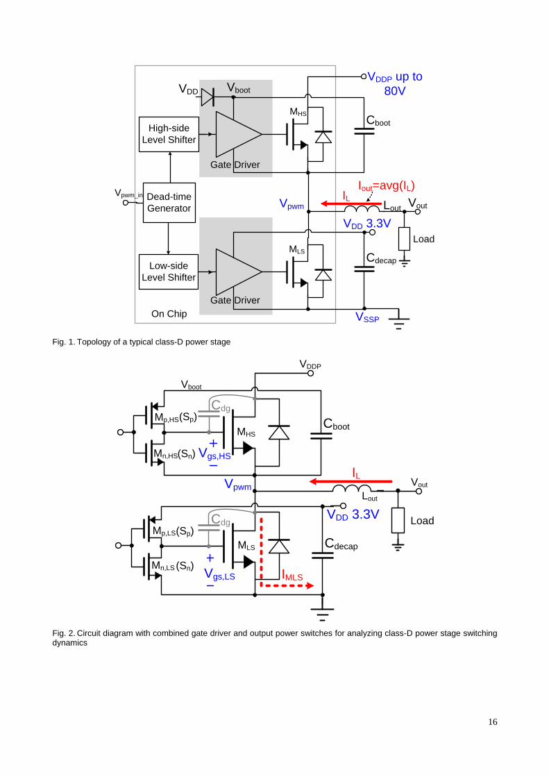
A typical class-D power stage for high-voltage high-power applications consists of two identical NDMOS
devices as High Side (HS) and Low Side (LS) switches as shown in Fig. 1 [2]-[7]. Since for DMOS power
transistors the maximum Vgs is typically much lower than the maximum Vds, the LS gate driver is supplied by a
separate low-voltage supply and externally decoupled. For the HS gate driver, an external bootstrapping
capacitor can be used as the supply. Here we use the three-line earth symbol for the power ground VSSP,
which is the off-chip reference ground. Later in the paper the single-line ground symbol will be adopted to
represent the on-chip grounds as to distinguish them from the off-chip reference ground. The circuit
parameters of this power stage used for the simulations in this paper are summarized in TABLE I. The
switching frequency fsw is chosen at 500kHz as a typical value of class-D fsw in general [2]-[9]. For

3
piezoelectric-actuator applications, a lower fsw can also be used if the signal bandwidth is lower. The output
DC current Iout is the average inductor current IL within one switching cycle. It is set at 1A with the output Vpwm
duty cycle being 0.5. This represents the scenario of the instant when the output stage is discharging the
capacitive piezoelectric load from mid-supply. Nevertheless, the analysis itself is general and also holds for
other output current and duty cycle combinations, as well as when the output stage is processing a dynamic
output signal.
A. Power Transistor Dissipation
The dominating power dissipation in the power MOSFETs of a high-voltage Class-D output stage consists
of three types of losses [10]: 1) Pcond: conduction loss caused by the power MOSFETs’ ron. 2) Pcap: capacitive
loss caused by charging and discharging parasitic capacitances on Vpwm, and 3) Psw : switching losses caused
by V-I overlap in the switches during switching transitions. Among the three dissipation sources, Pcond is
inversely proportional to the power transistor size S while Pcap is proportional to the power transistor size S. As
for Psw, in the optimal case (very fast switching) its dominant contribution is the intrinsic reverse-recovery
current [4] and this is also proportional to the power transistor size S. The total dissipation can then be
optimized by choosing the correct transistor size to balance the three power dissipation sources [10]. Under
the circuit operating conditions in TABLE I, an optimized DMOS power transistor size is derived as
56000µm/0.75µm, with TABLE II listing each dissipation source and their respective contributing ratio. This
optimization is considered in the ideal case, i.e. with no power supply parasitic inductances included.
Because our first attempt here is to examine what the dissipation sources should be and how they
contribute to the total dissipation in the optimal case, the driver stage (Fig. 2) for driving the two power
switches should also be designed to behave as close to ideal drivers as possible in this optimization. This has
two implications 1) the drivers should turn on the power switches very fast such that the main contribution to
V-I overlap is caused by the reverse-recovery current. Since we do not consider power supply parasitic
inductances in this phase, the driver pull-up transistor can be increased as much as necessary to reach this
minimum Psw. The minimized Psw is then proportional to the reverse-recovery charge in the body diode and
thus proportional to the power transistor size S. 2) The driver should turn off the power switches very fast and
then be able to completely keep the power switches off when required. Similarly since power supply parasitic
inductances are not considered yet, the driver pull-down transistor is sized to be much larger than the pull-up
transistor as to avoid cross conduction [7].

4
However, although switching can be arbitrarily fast in this optimization procedure, in reality it will cause
large di/dt, and consequently supply bounce which affects the circuit operation. In the following subsection we
will show how the gate drivers influence the supply bounce (di/dt) for different switching scenarios and how
efficiency deteriorates if supply bounce has to be limited by proper gate driver sizing.
B. Supply Bounce Analysis and Gate Driver Sizing
The switching behavior of a class-D output stage can be categorized into two types of switching transitions:
soft switching, where IL (dis)charges the parasitic output capacitance of the switch transistors and hard
switching, where the transistors (dis)charge these parasitics [11]. Depending on the relative amplitude of the
inductor ripple current and the load current, IL can either be bidirectional with both switching transitions being
soft switching or unidirectional, where one transition is soft switching and the other is hard switching. The
power stage circuit diagram in Fig. 2 is used to illustrate the two switching transitions. The load current IL is
flowing into the power stage and keeps flowing in this direction during the full switching cycle. Fig. 3(a) shows
the simulation waveforms in one complete switching cycle, consisting of soft and hard switching transitions
while Fig. 3(b) and Fig. 3(c) shows the two edges in detail.
In Fig. 3(b) for the soft switching transition edge, the Vpwm low-to-high transition starts when MLS is turning
off, and IL provides the current to charge Vpwm to VDDP without resorting to the active devices. From the driver
sizing point of view, when we look at the current flowing in MLS (IMLS), first, IMLS is decreased such that IL can
provide for the current necessary to charge the MLS parasitic capacitances and to discharge the MHS parasitic
capacitances. Then there comes a period where Vpwm is slewing and IMLS keeps nearly constant. When the
slewing is over, IMLS is further decreased to be conducted by the HS body diode within the dead time. During
both times when IMLS is decreasing, the di/dt is proportional to how fast MLS is being turned off, and thus is
proportional to the gate driver pull-down (PD) transistor Mn,ls size Sn.
For the hard switching transition as shown in Fig. 3(c), first MHS is turned off, and the current flows through
the MHS back-gate diode. Vpwm remains high until MLS has been turned on and has taken over all the load
current as well as the current for discharging the Vpwm node. The rate at which IMLS is increasing during this
time is proportional to the driver pull-up (PU) transistor Mp,LS size Sp. After that, Vpwm starts slewing with a rate
determined by Cdg,LS and the on resistance of Mp,LS (with size Sp). This slewing will also cause the MHS gate-
source voltage to rise through Cdg,HS and the on resistance of Mn,HS (with size Sn), so the driver PD transistor
Mn,HS should be sized with a much lower on resistance than PU transistor Mp,LS to avoid cross conduction.
5
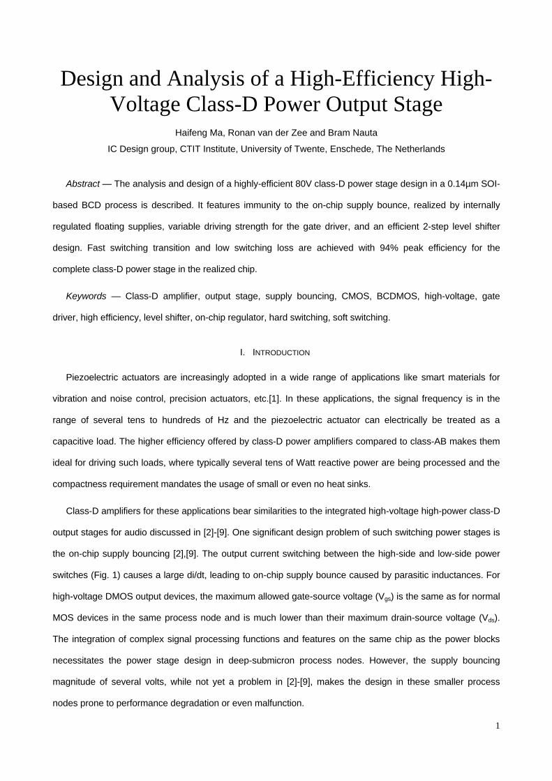
Because the HS and LS drivers and power switches are identical, the driver size versus di/dt analysis
made above also holds for the case that the Vpwm high-to-low transition is soft switching while the Vpwm low-to-
high is hard switching. The difference is that, since the HS gate driver supply is referred to Vpwm, the di/dt of
the current flowing in MHS and the subsequent supply bounce on VDDP will not influence the HS gate driver
supply. This will only be the case for class-D output stage topologies employing complementary output power
transistors [8].
In conclusion, regarding the relationship between the gate driver sizing and the switching dynamics, 1) Sn
is limited by the permissible di/dt in soft switching 2) Sp is limited by the permissible di/dt in hard switching,
and 3) Sp/Sn << 1 to prevent cross conduction during hard switching. From 1)-3) we further conclude that Sn in
soft switching is the major concern when it comes to supply bounce.
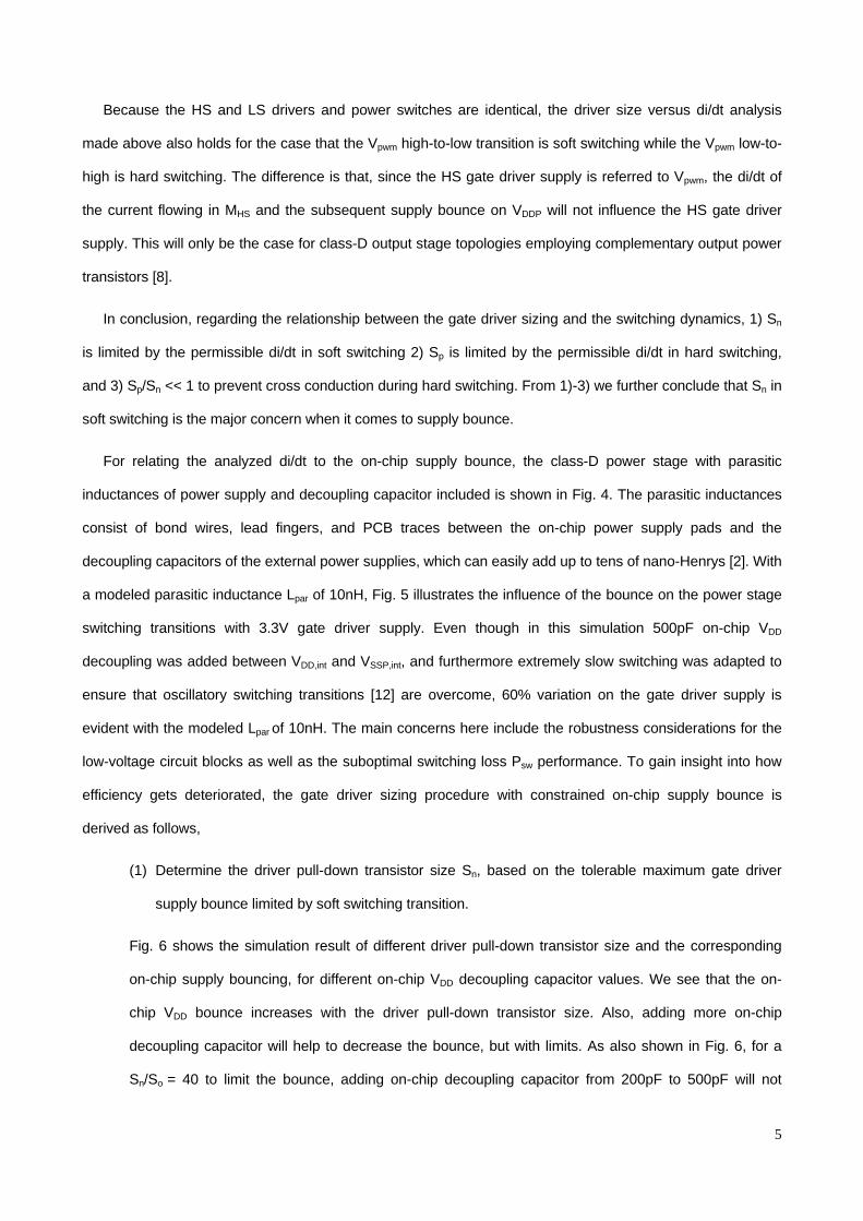
For relating the analyzed di/dt to the on-chip supply bounce, the class-D power stage with parasitic
inductances of power supply and decoupling capacitor included is shown in Fig. 4. The parasitic inductances
consist of bond wires, lead fingers, and PCB traces between the on-chip power supply pads and the
decoupling capacitors of the external power supplies, which can easily add up to tens of nano-Henrys [2]. With
a modeled parasitic inductance Lpar of 10nH, Fig. 5 illustrates the influence of the bounce on the power stage
switching transitions with 3.3V gate driver supply. Even though in this simulation 500pF on-chip VDD
decoupling was added between VDD,int and VSSP,int, and furthermore extremely slow switching was adapted to
ensure that oscillatory switching transitions [12] are overcome, 60% variation on the gate driver supply is
evident with the modeled Lpar of 10nH. The main concerns here include the robustness considerations for the
low-voltage circuit blocks as well as the suboptimal switching loss Psw performance. To gain insight into how
efficiency gets deteriorated, the gate driver sizing procedure with constrained on-chip supply bounce is
derived as follows,
(1) Determine the driver pull-down transistor size Sn, based on the tolerable maximum gate driver
supply bounce limited by soft switching transition.
Fig. 6 shows the simulation result of different driver pull-down transistor size and the corresponding
on-chip supply bouncing, for different on-chip VDD decoupling capacitor values. We see that the on-
chip VDD bounce increases with the driver pull-down transistor size. Also, adding more on-chip
decoupling capacitor will help to decrease the bounce, but with limits. As also shown in Fig. 6, for a
Sn/So = 40 to limit the bounce, adding on-chip decoupling capacitor from 200pF to 500pF will not
6
decrease the on-chip bounce anymore, primarily because the Lpar-Cdecap-on-chip bandwidth limits the
effectiveness of bounce suppression. Determine the driver pull-up transistor size Sp, limited with
respect to the pull-down transistor Sn for avoiding cross conduction of the two output power DMOS
switches.
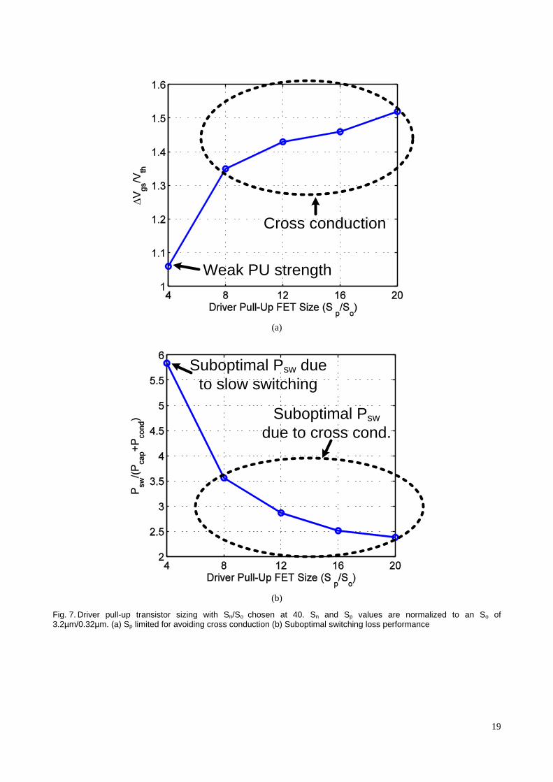
(2) Determine the driver pull-up transistor size Sp, limited with respect to the pull-down transistor Sn for
avoiding cross conduction of the two output power DMOS switches.
Considering the already limited Sn for suppressing the on-chip supply bounce, Sp is further limited by
the requirement to avoid cross conduction. This means that hard switching transitions have to be either
extremely slow or cause cross conduction, with both cases causing suboptimal switching loss. Fig.
7(a) shows the Sp sizing when Sn/So has been chosen at 40. The efficiency degradation caused by this
limitation is evident in Fig. 7(b).
An increase of Sp/So from 8 to 20 results in faster switching, which lowers Psw. However, a larger Sp
also results in cross conduction, adding to Psw, so Psw is not reduced to the optimal value compared to
the other losses Pcond + Pcap (optimum ratio should be 0.72 as in TABLE II).
Since the main factor that determines the power supply bouncing during switching transitions is the driver-
size-related di/dt, the analysis made above is not limited by the power transistor size chosen in TABLE II. If a
different power transistor size is chosen, the driver size will have to be scaled accordingly to meet the same
requirement on di/dt as well as on avoiding cross conduction. Consequently the design trade-offs for limiting
the di/dt in soft switching and aiming for fast transitions in hard switching are the same. Regarding the effect of
process and temperature variation on the on-chip supply bounce magnitude, the analysis of the relationship
between the driver transistor size and the bounce magnitude also holds. A decrease in temperature or a fast
process corner has the same effect as an increase in transistor size, which will cause more bounce.
Additionally, in designs where a larger Lpar than the modelled 10nH exists through longer decoupling loops,
e.g. larger packages than required or decoupling capacitors placed far away from the supply pins, the supply
bounce magnitude will also increase.

7
III. FLOATING GATE DRIVER TOPOLOGY
A. Supply-Regulated Floating Gate Driver
To overcome the on-chip driver supply bouncing issue without sacrificing efficiency during switching
transitions, we propose a gate driver topology with on-chip regulated floating supply. As shown in Fig. 8(a),
two on-chip voltage regulators are used to provide stable on-chip supply voltages to the gate driver circuits.
The two regulators track the two reference nodes VSSP,int and Vpwm respectively, so the on-chip bouncing will
not be seen by the driver circuits. The unregulated input supply voltage for the regulators are chosen based
on the estimated maximum bouncing magnitude plus the minimum operation voltage of the regulator circuits
(12V unregulated VDD is used here). The detailed gate driver circuit is shown in Fig. 8(b). The pull-up current
has been divided into two parts. The main Ipu is supplied by the unregulated VDD while an auxiliary Ipu is used
to turn the output power transistor fully on. By this configuration the regulators are not required to supply the
hundreds of milliamps for Ipu and their design can be simplified. For the pull-down current path, an in-cycle
variable gate driving strength is implemented and will be explained next.
B. In-Cycle Variable Gate-Driving Strength
As explained in the previous section, the main reason for excessive switching loss during hard switching is
because the driver PU transistor has to be much weaker than the PD transistor, other than limited by on-chip
bounce considerations. To circumvent this limitation of the driver PU strength, we propose to a use an in-cycle
variable gate-driving strength. As shown in Fig. 9(a), when the driver input and output status have both been
detected as already off, the combined strength of Mn1 and Mn2 will be used to keep the power transistor off
when the other driver is turning on based on the Sp/Sn driver ratio requirement. However, when the driver is in
the process of turning its output off and hasn’t yet reached the level determined by the Schmitt trigger, only
the weaker Mn1 will provide the pull-down current to turn off the output power transistor slowly in order to keep
di/dt low (Fig. 9(b)). This way we have the design freedom to both choose the correct Sp/Sn ratio to avoid
cross conduction, and limit the on-chip supply bounce. Simulation waveforms for comparing the effectiveness
with and without the adaptive driver turn-off strength are shown in Fig. 10, with the modeled Lpar of 10nH in the
simulation. Fig. 10(a) shows that the same effect for keeping the power transistor off is obtained while Fig.
10(b) illustrates that the supply bouncing is significantly reduced when a weaker PD strength can be applied
for turning the power transistor off. Fig. 10(a) and Fig. 10(b) are enlarged simulation waveforms within one
switching period.

8
C. Sizing of the Floating Gate Drivers
Compared with the sizing of the gate driver with externally decoupled low-voltage gate driver supply, the
sizing of the floating gate driver combined with the variable gate-driving strength can now have the following
advantages:
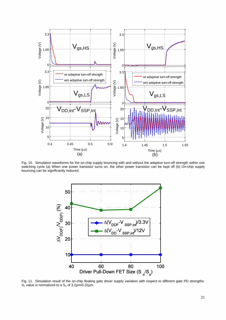
(1) The gate driver PD transistor can be sized larger, since the floating gate drivers can sustain a much
higher on-chip supply bouncing amplitude and the floating regulated driver supplies will not be directly
influenced.
As can be seen in Fig. 11, although the off-chip decoupled 12V supply still has large variations during
switching, the on-chip floating supply varies only 10% with the adopted floating regulator circuit discussed
in subsection D. This variation is mainly due to the load regulation of the regulator for providing the PU
current. Also, this clean gate driver supply is achieved without using area-consuming on-chip decoupling
capacitors in the hundred pF range.
(2) The PU transistor can be sized larger to improve efficiency without getting limited by the maximum
Sp/Sn ratio. Cross condition is avoided by the additional keep-off strength.
In Fig. 12(a) we see the effect of added keep-off strength to the PU transistor sizing. With the same
Sn/So=40 as used in Section II for limited bounce, 4x added keep-off strength can ensure that ∆Vgs is far
below Vth when choosing Sp/So up to 20. Fig. 12(b) shows that efficient hard switching transitions can be
realized since now larger PU transistor size can be adopted. With Sp/So set to 20, the Psw/(Pcon+Pcap) ratio
is now 0.73, close to the minimized Psw/(Pcon+Pcap) ratio of 0.72 in TABLE II.
D. On-chip Floating Voltage Regulator
The on-chip floating regulator circuit for both HS and LS is shown in Fig. 13. For fast response and low
output voltage ripple, the output VDDF/VDDF,boot has been excluded from the feedback loop [13]. The drawback
on precision is not critical here since the regulator supplies mainly digital blocks. The output devices of the
regulator are also DMOS devices to sustain the higher 12V unregulated VDD as well as the bouncing
superimposed on it.
On-chip decoupling capacitor CG is important for power supply ripple rejection. It is vital to minimize its
parasitic capacitance Cpar,sub to the substrate as any disturbance from the VSSP, int/Vpwm node will be coupled to
VB by a ratio Cpar,sub/(CG+Cpar,sub). As an example, the output voltage VPWM slews 80V in a few nanoseconds;

9
even with 1% parasitic capacitance 0.8V will be coupled to the 3.3V output, which is an unacceptable 25%
variation. Consequently it is rather important that these decoupling capacitors are fully shielded from the
substrate as shown in Fig. 13. Here for the metal fringe capacitor the whole first metal plate is connected to
the VSSP,int/Vpwm node such that VB is fully shielded. The output decoupling capacitor Cout has a value of 20pF,
which is much more area efficient than the decoupling capacitor of an unregulated gate-driver supply (Fig. 6).
Efficient switching transitions as shown in Fig. 14 are achieved by this gate driver topology. The on-chip
floating regulators provide a reliable 3.3V supply to the gate driver circuit during both soft- and hard-switching
transients. Also, thanks to the in-cycle variable gate-driving strength, the high-to-low hard switching here is
performed fast, simultaneously avoiding cross conduction and excessive bounce on the off-chip decoupled
12V supply (Fig. 10).
IV. POWER-EFFICIENT 2-STEP LEVEL SHIFTER
Another important circuit block for the class-D power stage is the level shifter circuit [14]-[17]. It is used for
communication between signals referred to the digital ground VSSD and those referred to the power ground
VSSP,int or the floating HS Vpwm, as shown in Fig. 15. With a 3.3V supply for both the low-voltage control blocks
and the gate drivers, the on-chip supply bouncing magnitude higher than the 3.3V supply itself presents a
challenge for reliable level shifting. As shown in Fig. 15, the >3.3V bounce causes the voltage potential
between VDDF and VSSD to be very uncertain. This makes conventional level shifting by building a direct
interface circuit using VDDF and VSSD as power and ground [2], [14], [15] not feasible. For reliable level shifting,
a two-step approach has been adopted here, where the voltage level is first referred to the higher 12V VDD,int
and then to VSSP,int.
In addition, compared to level shifters used for transferring to voltage levels referred to fixed supply rails
[8], [16], [17], level shifting to the slewing Vpwm is associated with disturbance that could corrupt the transferred
signal. We consider the SR latch referred to the Vpwm voltage domain as shown in Fig. 16. The supply rail
referred to Vpwm has the same high slew rate as Vpwm (up tp 10kV/s in this design). If there exist parasitic
capacitances e.g. to the substrate at the input of the latch, and the stage preceding the latch has a resistive
load, this directly translates to a common-mode disturbance for the latch and a possible logic output error can
occur.
To cope with the >3.3V supply bounce, the two-step level shifting approach is shown in the circuit
schematic in Fig. 17, where the voltage level is first referred to the higher 12V VDD,int and then to VSSP,int. As

10
shown in Fig. 17, the already available 12V VDD,int referred to VSSD is not influenced too much by the bounce
and thus establishing a reliable interface circuit across VDD,int and VSSD as the 1st level shifting step.
Subsequently the 2nd
level shifting transfers the signal to the one referred to VSSP,int, tolerating the supply
voltage variation between VDD,int and VSSP,int.
For the HS level shifter circuit, the power dissipation could be significant because the current for
transferring the signal has to flow between the maximum 92V Vboot,int and ground. Two approaches have been
implemented in the level shifter circuit of Fig. 17 to minimize its power dissipation and make it power efficient
for HS usage. Firstly, pulsed set and reset input are applied such that only pulsed current are bridging most of
the 92V [15]. Additionally, we introduce an active load (transistors M1-M4) with partial positive feedback
characterized by a lower impedance for common-mode disturbances like VDD,int or Vpwm, and a higher
impedance for the differential-mode signal pulses. The diode-connected M1 and M4 are configured with
slightly larger W/L ratio compared with the cross-coupled M2 and M3. From a large-signal perspective,
approximately 2x larger (M1+M2) and (M3+M4) are used for conducting the common-mode disturbance
current Icm,disturb while only M1 or M4 are used for conducting the signal current Idm,sig. This way, compared to
using a simple active load [14], significantly lower current pulses can be applied in the first level shifting while
maintaining its common-mode noise immunity. Concluding, with the introduction of a two-step level shifting,
pulsed set/reset signaling as well as an active load with partial positive feedback, the level shifter circuit
shown in Fig. 17 can deal with the design challenges for both HS and LS and thus identical circuits are used
for both HS and LS level shifting.
V. MEASUREMENT RESULTS
The 80V power output stage has been fabricated in NXP A-BCD9, a 0.14µm SOI-based BCD process and
the chip photograph is shown in Fig. 18. For the layout of the power stage, two bondpads are used for each of
the VDDP, VSSP and Vpwm pins to ensure enough current handling capability. The top-metal layer connected to
these power supply bondpads is triangular (as is evident in the chip photograph in Fig. 18) to realize a uniform
current density, resulting in minimal metal resistance in the power transistors.
Packaged chips are used for all the measurements that follow, with external heat sinks attached to the
package for thermal stability considerations. Off-chip decoupling capacitors are required for the decoupling of
the following critical voltage domains: high-voltage power supply VDDP/VSSP, LS gate driver supply VDD/VSSP,
HS gate driver bootstrapped supply Vboot/Vpwm. Minimum current loops [2] should be ensured in the PCB
11
design for these decoupling loops as to minimize Lpar. Two power supplies are required: the 12V gate-driver
supply as well as the 80V high-voltage power supply.
For measuring efficiency, first a current-source load instead of the capacitive piezoelectric load is used to
make the power stage delivering active output power. When the output voltage is fixed, the output power is
varied by sweeping the output current value of the current-source load, and the output power is dissipated in
this load. For a fixed output voltage of 40V (duty cycle of 0.5) and a switching frequency of 230kHz as well as
530kHz, the efficiency measurement results are shown in Fig. 19. The measured peak efficiency for 230kHz
switching frequency is 94%. For power efficiency measurements when driving capacitive piezoelectric load, a
series-connected 23µF+1.6Ω is used to model the piezo-actuator [1] and this load is mostly capacitive at the
input signal frequency fsig of several tens to hundreds of Hz. Efficiency is defined here as
Eff = Pout,app/(Pout,app+Pd),
where Pout,app is the apparent output power Vout,rms*Iout,rms (VA) processed by the amplifier and Pd is the total
amplifier dissipation. Even though there will be no real power delivered to the load for the purely capacitive
load case, this expression for power efficiency (Eff) can still be used to characterize the power stage
efficiency, since it is based on how much will be dissipated (Pd) when processing a certain amount of power
(Pout,app). Fig. 20 shows the measurement results with a 500Hz signal applied on the load and maximum
Pout,rms of 45VA. The peak efficiency is 92% and 89% for switching frequency of 230kHz and 530kHz
respectively. The current supplied by both the 12V and 80V supply are taken into account for all of these
power efficiency measurements.
For measuring linearity, the power stage is operated within a hysteretic-based feedback loop [18]-[20]. For
a 1st-order hysteretic-based loop [20] with the switching frequency set at 230kHz for D=0.5, Fig. 21 shows the
THD+N performance when driving a series-connected 2.2µF+3Ω load. A THD+N of 0.03% is achieved for
fsig=1kHz, which is comparable to [20]. Compared with the case of fsig=1kHz, THD+N level will increase for the
fsig=2kHz case. This is mainly because the output power is higher due to the capacitive load, and the loop gain
of the feedback loop for suppressing the harmonics of the 2kHz signal is lower than the loop gain in the 1kHz
case.
Compared to other power stage designs, this design offers the best possibilities for integration with other
mixed-signal functions and especially digital circuitry thanks to the smaller process node being used, 0.14m
versus 0.25–3m in [2]-[9]. This is permitted by the supply bounce immunity features, enabling its operation

12
with a 3.3V Vgs other than 5-12V Vgs in [2]-[8] and 18V Vgs=Vds in [9]. The >90% peak efficiency compares
favorably with [2]-[9]. This is also ensured by the supply-bouncing immunity, as well as by the in-cycle variable
gate drive strength.
VI. CONCLUSIONS
Fast switching transitions are crucial for minimizing class-D switching losses. In this paper the gate driver
sizing issues considering the on-chip supply bounce are discussed in detail. It is shown that for traditional gate
driver circuits both the pull-up and pull-down strength have to be limited to avoid excessive supply bounce and
this in turn limits the realization of power-efficient fast switching transitions. The introduction of regulated
floating supplies, variable driving strength for the gate driver and a 2-step level shifter ensure fast switching
transitions not disturbed by on-chip supply bounce. A high-voltage, high-power class-D power stage with 3.3V
Vgs is realized and measures with over 94% peak efficiency.
ACKNOWLEDGMENT
This research is funded by the Dutch Technology Foundation STW (project No. 10602). We thank NXP for
silicon donation.
REFERENCES
[1] C. Wallenhauer, et al, ―Efficiency-improved high-voltage analog power amplifier for driving piezoelectric actuators,‖ IEEE Trans. Circuits Syst. I, Reg. Papers, vol. 57, no. 1,pp. 291–298, Jan. 2010.
[2] M. Berkhout, ―An integrated 200-W class-D audio amplifier,‖ IEEE J. Solid-State Circuits, vol. 38, no. 7, pp. 1198–1206, Jul. 2003
[3] F. Nyboe, et al, ―A 240W monolithic class-D audio amplifier output stage,‖ in ISSCC Dig. Tech. Papers, pp.1346-1355, Feb., 2006.
[4] M. Berkhout, ―A 460W class-D output stage with adaptive gate drive,‖ in ISSCC Dig. Tech. Papers, pp.452-453, Feb., 2009.
[5] B. Krabbenborg and M. Berkhout, ―Closed-loop class-D amplifier with nonlinear loop integrators,‖ IEEE J. Solid-State Circuits, vol. 45, no. 7, pp. 1389–1398, Jul. 2010.
[6] P. P. Siniscalchi and R. K. Hester, ―A 20 W/channel class-D Amplifier with near-zero common-mode radiated emissions,‖ IEEE J. Solid-State Circuits, vol. 44, no. 12, pp. 3264–3271, Dec. 2009.
[7] M. Berkhout, ―A Class D Output Stage with Zero Dead Time,‖ ISSCC Dig. Tech. Papers, pp. 134-135, Feb., 2003.
[8] P. Morrow, E. Gaalaas, and O. McCarthy, ―A 20-W stereo class-D audio output power stage in 0.6-µm BCDMOS technology,‖ IEEE J. Solid-State Circuits, vol. 39, no. 11, pp. 1948–1958, Nov. 2004.
[9] J. Liu, et al, ―A 100 W 5.1-Channel Digital Class-D Audio Amplifier With Single-Chip Design,‖ IEEE J. Solid-State Circuits, vol. 47, no. 6, pp. 1344–1354, June. 2012.
[10] J. S. Chang, M. T. Tan, Z. Cheng, and Y. C. Tong, ―Analysis and design of power efficient class D amplifier output stages,‖ IEEE Trans. Circuits Syst. I, vol. 47, pp. 897–902, June 2000.
[11] M. Berkhout, L. Breems, and E. van Tuijl, ―Audio at low and high power,‖ in Proc. ESSCIRC, Sep. 2008, pp. 40–49.
[12] H. Ma, R. van der Zee, and B. Nauta, ―An Integrated 80-V Class-D Power Output Stage with 94% Efficiency in a 0.14µm SOI BCD Process ‖, in Proc. ESSCIRC, Sep. 2013, pp. 89–92.
[13] G. W. den Besten and B. Nauta, ―Embedded 5 V-to-3.3 V voltage regulator for supplying digital IC’s in 3.3 V technology,‖ IEEE J. Solid-State Circuits, vol. 33, no. 7, pp. 956–962, Jul. 1998
[14] M. C. W. Høyerby, M. A. E. Andersen, and P. Andreani, ―A 0.35μm 50V CMOS Sliding-Mode Control IC for Buck Converters,‖ in Proc. ESSCIRC, Sep. 2007, pp. 182–185
[15] M. A. Huque, et al, ―Siliconon-insulator-based high-voltage, high-temperature integrated circuit gate driver for silicon carbide-based power field effect transistor,‖ IET Proc.Power Electron., vol. 3, no. 6, pp. 1001–1009, Nov. 2010
[16] Y. Moghe, T. Lehmann, and T. Piessens, ―Nanosecond delay floating high voltage level shifters in a 0.35 m HV-CMOS technology,‖ IEEE J. Solid-State Circuits, vol. 46, pp. 485–497, 2011.
[17] J. Borg and J. Johansson, ―An ultrasonic transducer interface IC with integrated push-pull 40 Vpp, 400 mA current output, 8-bit DAC and integrated HV multiplexer,‖ IEEE J. of Solid-State Circuits, vol. 46, no. 2, pp. 475-484, Feb. 2011.
[18] M. Hoyerby and M. Andersen, ―Carrier distortion in hysteretic self-oscillating class-D audio power amplifiers: Analysis and optimization,‖ IEEE Trans. Power Electron., vol. 24, no. 3, pp. 714–729, 2009.

13
[19] J. Lu and R. Gharpurey, ―Design and analysis of a self-oscillating class-D audio amplifier employing a hysteretic comparator,‖ IEEE J. Solid-State Circuits, vol. 46, no. 10, pp. 2336–2349, Oct. 2011.
[20] R. Cellier, A. Nagari, H. Souha, G. Pillonnet, and N. Abouchi, "A synchronized self oscillating Class-D amplifier for mobile application," in Proc. ESSCIRC, Sep. 2012, pp. 422-425.

14
Figure Captions:
Fig. 1. Topology of a typical class-D power stage
Fig. 2. Circuit diagram with combined gate driver and output power switches for analyzing class-D power
stage switching dynamics
Fig. 3. Simulation waveforms with both Vpwm soft switching and hard switching transitions. (a) One complete
switching cycle (b) Soft switching transition (c) Hard switching transition
Fig. 4. Class-D power stage with power supply parasitic inductance included
Fig. 5. Simulation waveforms illustrating the influence of supply bouncing, Vpwm high-to-low transition has to
be extremely slow and results in high switching loss.
Fig. 6. Simulation result of different driver pull-down transistor size and the corresponding on-chip supply
bouncing, under different on-chip decoupling capacitor values, Sn value is normalized to a So of
3.2µm/0.32µm.
Fig. 7. Driver pull-up transistor sizing with Sn/So chosen at 40. Sn and Sp values are normalized to an So of
3.2µm/0.32µm. (a) Sp limited for avoiding cross conduction (b) Suboptimal switching loss performance
Fig. 8. Proposed power stage topology (a) supply bouncing influence on the functionality of the gate driver is
eliminated by the on-chip regulated gate-driver supply (b) Detailed gate driver structure.
Fig. 9. Gate driver with adaptive turn-off strength (a) Stronger pull-down transistors for keeping the power
transistor off (b) Weaker pull-down transistors for turning the power transistor off
Fig. 10. Simulation waveforms for the on-chip supply bouncing with and without the adaptive turn-off strength
within one switching cycle (a) When one power transistor turns on, the other power transistor can be kept off
(b) On-chip supply bouncing can be significantly reduced.
Fig. 11. Simulation result of the on-chip floating gate driver supply variation with respect to different gate PD
strengths. Sn value is normalized to a So of 3.2µm/0.32µm.
Fig. 12. Simulation result of using different driver PU strengths, with Sn/So chosen at 40. Sn and Sp values are
normalized to a So of 3.2µm/0.32µm. (a) Cross conduction is prevented by adding additional keep-off strength
of 4xSn. (b) Fast hard switching transitions are realized with much smaller switching loss compared with the
case using off-chip decoupled 3.3V gate driver supply.

15
Fig. 13. On-chip regulator and its decoupling capacitor CG implementation
Fig. 14. Simulation waveforms of the power stage in Fig. 8, Vpwm high-to-low transition is fast, without
disturbing the on-chip floating driver supply.
Fig. 15. Illustration of the communication between different voltage domains by the level shifter
Fig. 16. Slewing for the voltage levels referred to Vpwm can cause error output of the level shifter.
Fig. 17. Level shifter circuit and illustration of the on-chip supply/ground waveforms which necessitates a 2-
step approach for the level shifting
Fig. 18. Chip photograph of the 80V class-D power stage
Fig. 19. Power efficiency and dissipation measurement results for 230kHz and 530kHz switching frequency,
the measurement is with a DC electronic load for delivering real output power.
Fig. 20. Apparent power efficiency (see text) and dissipation measurement results for 230kHz and 530kHz
switching frequency driving a series-connected 23µF capacitor and 1.6Ω resistor.
Fig. 21. Measured linearity performance of the class-D output stage within a 1st-order hysteretic feedback
loop, with a series-connected 2.2µF+3Ω load.
Table Captions:
TABLE I. Summary of the parameters used in the power stage simulation
TABLE II. List of each dissipation source with an optimized power transistor size S of 56000µm/0.75 µm
16
Fig. 1. Topology of a typical class-D power stage
Lout
Mn,LS
Mn,HS
Mp,HS
MLS
MHS
VDDP
Vgs,LS
Vgs,HS
Vboot
ILVout
Load
Vpwm
Cdecap
VDD 3.3V
Cboot
IMLS
Cdg
Cdg
Mp,LS
(Sn)
(Sp)
(Sn)
(Sp)
Fig. 2. Circuit diagram with combined gate driver and output power switches for analyzing class-D power stage switching dynamics
VDDP up to
80V
Cboot
Vboot
High-side
Level Shifter
Gate Driver
Gate Driver
LoutVout
Load
Low-side
Level Shifter
VSSPOn Chip
Dead-time
Generator
Vpwm_in
VDD
Cdecap
VDD 3.3V
MLS
MHS
Vpwm
ILIout=avg(IL)

17
0
1.65
3.3
Vo
lta
ge
(V
)
0
1.65
3.3
Vo
lta
ge
(V
)
0
40
80
Vo
lta
ge
(V
)
0.39 0.4 0.41 0.42 0.43 0.44 0.45
0
0.5
1
1.5
Time (s)
Cu
rre
nt (A
)
0
1.65
3.3
Vo
lta
ge
(V
)
0
1.65
3.3
Vo
lta
ge
(V
)
0
40
80
Vo
lta
ge
(V
)
1.49 1.5 1.51 1.52 1.53 1.54 1.55
0
0.5
1
1.5
2
Time (s)
Cu
rre
nt (A
)
0
1.65
3.3
Vo
lta
ge
(V
)
0
1.65
3.3
Vo
lta
ge
(V
)0
40
80
Vo
lta
ge
(V
)
0 0.5 1 1.5 2
0
0.5
1
1.5
2
Time (s)
Cu
rre
nt (A
)
Vgs,HS
Vgs,LS
Vpwm
IMLS
(a)
(b) (c)
Vgs,HS
Vgs,LS
Vpwm
IMLS
Vgs,LS
Vpwm
IMLS
di/dt∝Sndi/dt∝Sp
Vgs,HS
∆Vgs∝Sn/Sp
Fig. 3. Simulation waveforms with both Vpwm soft switching and hard switching transitions. (a) One complete switching cycle (b) Soft switching transition (c) Hard switching transition
0
1.65
3.3
Volta
ge (V
)
0
1.65
3.3
Volta
ge (V
)
0
5
10
Volta
ge (V
)
0
40
80
Volta
ge (V
)
0
1
2
Curre
nt (A
)
0 0.5 1 1.5 20
2
4
6
Time (s)
Ener
gy (
J)
Lout
Mn,LS
Mp,LS
Mn,HS
Mp,HS
VDD,int
MLS
MHS
VDDP
Vgs,LS
Vgs,HS
Vboot,int
ILVout
Load
Vpwm
VSSP,int
Cdecap
VDD 3.3V
Lpar 10nH
modeled
Cboot
Chip Boundary
IMLS
(Sn)
(Sp)
(Sn)
(Sp)Cdg
Cdg
Fig. 4. Class-D power stage with power supply parasitic inductance included

18
0
1.65
3.3
Vo
lta
ge
(V
)
0
1.65
3.3
Vo
lta
ge
(V
)
2
4
6
Vo
lta
ge
(V
)
0
40
80
Vo
lta
ge
(V
)
0 0.5 1 1.5 2
0
0.5
1
1.5
Time (s)
Cu
rre
nt (A
)
Vgs,HS
Vgs,LS
Vpwm
IMLS
VDD,int-VSSP,int
Fig. 5. Simulation waveforms illustrating the influence of supply bouncing, Vpwm high-to-low transition has to be extremely slow and results in high switching loss.
Limited Sn
Fig. 6. Simulation result of different driver pull-down transistor size and the corresponding on-chip supply bouncing, under different on-chip decoupling capacitor values, Sn value is normalized to a So of 3.2µm/0.32µm.
19
Cross conduction
Weak PU strength
(a)
Suboptimal Psw
due to cross cond.
Suboptimal Psw due
to slow switching
(b)
Fig. 7. Driver pull-up transistor sizing with Sn/So chosen at 40. Sn and Sp values are normalized to an So of 3.2µm/0.32µm. (a) Sp limited for avoiding cross conduction (b) Suboptimal switching loss performance

20
MLS
MHSCboot
VDDF 3.3V refered to VSSP,int
Off chipOn chip
Lout
Cdecap
Regulator
Regulator
DbootVboot, int
VDD, int
VDD, int
Gate Driver
Gate Driver
VpwmVout
Load
VSSP,int
Vpwm
Ipu,aux Ipu,main
Ipu,aux Ipu,main
VSSP 0V
VDDP up to
80V
VDD 12V
nominal
VDDF,boot 3.3V refered to Vpwm
Vgs,LS
Vgs,HS
IL
Vgs,LS
(Vgs,HS)
VDDF(VDDF,boot)
on-chip generated
VDD,int(Vboot,int)
externally supplied
VSSP,int(Vpwm)
Ipu,aux
Ipu,main
Mn1 Mn2
Ipu
(b)
(a)
Adaptive turn-off strength
Lpar 10nH
modeled
Fig. 8. Proposed power stage topology (a) supply bouncing influence on the functionality of the gate driver is eliminated by the on-chip regulated gate-driver supply (b) Detailed gate driver structure.
Keeping the power FET off
Mn1 Mn2
k*Ipu
IN
Mn1 Mn2
Ipd
Turning the power FET off
IN
Vgs,LS
(Vgs,HS)Vgs,LS
(Vgs,HS)
Fig. 9. Gate driver with adaptive turn-off strength (a) Stronger pull-down transistors for keeping the power transistor off (b) Weaker pull-down transistors for turning the power transistor off
21
0
1.65
3.3
Vo
lta
ge
(V
)
0
1.65
3.3
Vo
lta
ge
(V
)
0.4 0.45 0.5 0.55
5
10
15
20
Time (s)
Vo
lta
ge
(V
)
w/ adaptive turn-off strength
w/o adaptive turn-off strength
0
1.65
3.3
Vo
lta
ge
(V
)
0
1.65
3.3
Vo
lta
ge
(V
)
1.4 1.45 1.5 1.55
5
10
15
20
Time (s)
Vo
lta
ge
(V
)
w/ adaptive turn-off strength
w/o adaptive turn-off strength
(a) (b)
Vgs,LS
VDD,int-VSSP,int
Vgs,HS Vgs,HS
Vgs,LS
VDD,int-VSSP,int
Fig. 10. Simulation waveforms for the on-chip supply bouncing with and without the adaptive turn-off strength within one switching cycle (a) When one power transistor turns on, the other power transistor can be kept off (b) On-chip supply bouncing can be significantly reduced.
Fig. 11. Simulation result of the on-chip floating gate driver supply variation with respect to different gate PD strengths. Sn value is normalized to a So of 3.2µm/0.32µm.

22
(a)
(b)
Fig. 12. Simulation result of using different driver PU strengths, with Sn/So chosen at 40. Sn and Sp values are normalized to a So of 3.2µm/0.32µm. (a) Cross conduction is prevented by adding additional keep-off strength of 4xSn. (b) Fast hard switching transitions are realized with much smaller switching loss compared with the case using off-chip decoupled 3.3V gate driver supply

23
Vref
Iout
VB
VSSP,int(Vpwm)
VDD,int(Vboot,int)
VDDF(VDDF,boot)
BGR
Cpar,sub
Cpar,sub
CG
CoutFirst metal layer
Higher metal layer
Vias
VB
VSSP,int(Vpwm)
Fig. 13. On-chip regulator and its decoupling capacitor CG implementation
0
1.65
3.3
Vo
ltag
e (
V)
0
1.65
3.3
Vo
ltag
e (
V)
2
3
4
Vo
ltag
e (
V)
0
40
80
Vo
ltag
e (
V)
0 0.5 1 1.5 2
0
0.5
1
1.5
2
Time (s)
Cu
rre
nt (
A)
Vgs,HS
Vgs,LS
Vpwm
IMLS
VDDF-VSSP,int
Fig. 14. Simulation waveforms of the power stage in Fig. 8, Vpwm high-to-low transition is fast, without disturbing the on-chip floating driver supply.

24
0 0.005 0.01 0.015-6
-4
-2
0
2
4
6
8
10
12
14
PWM Gen.
& Control
Regulator
VDD, int
Gate Driver
VSSP,int
VDDF
High-side
Level Shifter
Low-side
Level Shifter
Regulator
Vboot, int
Gate Driver
Vpwm
VDDF,boot
Vgs,LS
Vgs,HS
VSSP
VDD
Vpwm
Vboot
VDDD
VSSD
VSSD, reference ground VSSP,int
3.3V
VDDDVDDF
Fig. 15. Illustration of the communication between different voltage domains by the level shifter
S
R
Q
Cpar
Idisturb
IsigCpar
Idisturb
Isig
RL RL
Sig
Vpwm
Fig. 16. Slewing for the voltage levels referred to Vpwm can cause error output of the level shifter

25
CparCpar
Vb
Vout
VSSD
Pulsed
Set
2nd
Level ShiftVDD,int(Vboot,int)
VSSP,int(Vpwm)
1st Level Shift
VDDF(VDDF,boot)
M1 M2M3 M4
Pulsed
Reset
Icm,disturb Icm,disturb
Idm,sig
0 0.005 0.01 0.015-6
-4
-2
0
2
4
6
8
10
12
14
VSSP,int
VDDF
VDD,int
3.3V
12V
VSSD, reference ground
Fig. 17. Level shifter circuit and illustration of the on-chip supply/ground waveforms which necessitates a 2-step approach for the level shifting
25
50
µm
2480µm
HS & LS Power DMOSFETs
Gate Drivers
Regulator RegulatorLevel
Shifters, etc.
Fig. 18. Chip photograph of the 80V class-D power stage

26
Fig. 19. Power efficiency and dissipation measurement results for 230kHz and 530kHz switching frequency, the measurement is with a DC electronic load for delivering real output power.
Fig. 20. Apparent power efficiency (see text) and dissipation measurement results for 230kHz and 530kHz switching frequency driving a series-connected 23µF capacitor and 1.6Ω resistor.

27
Pout,rms=18VA
Pout,rms=9VA
Fig. 21. Measured linearity performance of the class-D output stage within a 1st-order hysteretic feedback loop, with a
series-connected 2.2µF+3Ω load.
TABLE I. SUMMARY OF THE PARAMETERS USED IN THE POWER STAGE SIMULATION
Parameters Value
Power Stage Supply VDDP 80V
DMOSFET’s Maximum Vgs 3.3V
Output Inductance Lout 100µH
Switching Frequency fsw 500kHz
Output DC Current Iout 1A
Vpwm Duty Cycle 0.5
Dead Time td 100ns
TABLE II. LIST OF EACH DISSIPATION SOURCE WITH AN OPTIMIZED POWER TRANSISTOR SIZE S OF 56000µm/0.75µm
Dissipation Source Power Loss Type Power Loss Ratio
Total Output DMOSFETs’ Loss Balanced 1.2W 100%
Pcond ∝ 1/S 570mW 48%
Pcap ∝ S 120mW 10%
52%
Psw ∝ S 510mW 42%

28
Haifeng Ma (S’13) received the B.S. degree in Physics from Nanjing University, Nanjing, China, in 2007, and
the M.S. degree (with Honor) in Microelectronics from Fudan University, Shanghai, China, in 2010. The
same year, he joined the IC Design group at the University of Twente, Enschede, The Netherlands, as a
Ph.D. student.
His research interest is in analog IC design, with current focus on switching power amplifiers.
Ronan van der Zee (M’07) received the M.Sc. degree (cum laude) in electrical engineering from the
University of Twente, Enschede, the Netherlands in 1994. In 1999, he received the Ph.D. degree from the
same university on the subject of high-efficiency audio amplifiers. In 1999, he joined Philips Semiconductors,
where he worked on class AB and class D power amplifiers. In 2003, he joined the IC Design group at the
University of Twente. His current research interests include linear and switching power amplifiers, RF
frontends and wireless sensor networks.

29
Bram Nauta (F’08) was born in Hengelo, The Netherlands. In 1987 he received the M.Sc degree (cum
laude) in electrical engineering from the University of Twente, Enschede, The Netherlands. In 1991 he
received the Ph.D. degree from the same university on the subject of analog CMOS filters for very high
frequencies. In 1991 he joined the Mixed-Signal Circuits and Systems Department of Philips Research,
Eindhoven the Netherlands. In 1998 he returned to the University of Twente, as full professor heading the IC
Design group. His current research interest is high-speed analog CMOS circuits.
He served as Associate Editor of IEEE Transactions on Circuits and Systems II (1997-1999). He was Guest
Editor, Associate Editor (2001-2006) and later the Editor-in-Chief (2007-2010) of IEEE Journal of Solid-State
Circuits. He was member of the technical program committee of the International Solid State Circuits
Conference (ISSCC) where he served in several roles including the European Chair and the 2013 Program
Chair. He also served in the Technical Program Committee of the Symposium on VLSI circuits (2009-2013)
and is in the steering committee and programme commitee of the European Solid State Circuit Conference
(ESSCIRC). He is co-recipient of the ISSCC 2002 and 2009 "Van Vessem Outstanding Paper Award". He
served as distinguished lecturer of the IEEE, is member of IEEE-SSCS AdCom and is IEEE fellow.