design and analysis of custom clock buffers and a d flip ... · design and analysis of custom clock...
TRANSCRIPT
Design and Analysis of Custom Clock Buffers and a D Flip-Flop for Low Swing Clock Distribution Networks
A Thesis presented
by
Mallika Rathore
to
The Graduate School
in Partial Fulfillment of the
Requirements
for the Degree of
Master of Science
in
Electrical Engineering
Stony Brook University
May 2014

Stony Brook University
The Graduate School
Mallika Rathore
We, the thesis committee for the above candidate for the
Master of Science degree, hereby recommend
acceptance of this thesis
Dr. Emre Salman - Thesis AdvisorAssistant Professor, Department of Electrical and Computer Engineering
Dr. Milutin Stanacevic - Second ReaderAssociate Professor, Department of Electrical and Computer Engineering
This thesis is accepted by the Graduate School
Charles TaberDean of the Graduate School
ii

Abstract of the Thesis
Design and Analysis of Custom Clock Buffers and a D Flip-Flop for Low Swing Clock Distribution Networks
by
Mallika Rathore
Master of Science
in
Electrical Engineering
Stony Brook University
2014
With higher integration, power has become a primary concern for IC design.Clock signal has the highest switching activity and can be responsible for up to40% of the overall power dissipation due to large clock network capacitance. Thisdissertation presents an approach to reduce this power consumption by providinga 30% reduction in the clock swing, which is accomplished by custom reduced-swing buffers. The objective is to reduce the clock swing without implementing anadditional low supply voltage, while also satisfying the slew constraints at mul-tiple process, voltage and temperature (PVT) corners. The low swing buffer isdesigned using 1V 45nm NCSU technology and the clock frequency consideredfor this analysis is 1.5GHz. As compared to a conventional buffer, approximately14% reduction in the dynamic power consumption is achieved while driving aload capacitance of 50fF and maintaining the same clock slew. A novel D flip-flop(DFF) architecture that can operate with a low swing clock is also proposed andcompared with existing designs. These architectures are simulated consideringa clock and data frequency of 1.5GHz and 150MHz, respectively. In compari-son with the other low swing topologies, the proposed low swing DFF topologyprovides an average reduction of 33.6% and 39.5% in, respectively, the overalldynamic power dissipation and power-delay product. The robustness of the DFF
iii

architectures is also evaluated for different PVT corners. This comparative analy-sis demonstrates an average improvement of 19.34% and 38.91% in, respectively,CLK-to-Q delay and dynamic power dissipation for the proposed topology. Fi-nally, a low swing clock distribution network is designed and analyzed by com-bining the custom reduced swing buffers and the proposed DFF architecture. Re-liable operation is demonstrated considering a large fan-out of 50 DFFs at theoutput of the reduced swing buffers.
iv

Dedication Page
To my late grandparents, Mr. Ranvir Singh Shastri and Mrs. Snehlata Singh,and to my loving parents, Mr. Devendra Singh Rathore and Mrs. Nivedita Rathore.
v

Table of ContentsAbstract iii
List of Figures vii
List of Tables viii
Acknowledgement ix
1 Introduction 1
2 Custom Clock Buffer Design for Low Swing Operation 42.1 Existing Reduced Swing Buffers . . . . . . . . . . . . . . . . . . 52.2 Modified Reduced Swing Buffers . . . . . . . . . . . . . . . . . . 62.3 Simulation Results . . . . . . . . . . . . . . . . . . . . . . . . . 8
2.3.1 Comparative analysis . . . . . . . . . . . . . . . . . . . . 112.3.2 Full swing to reduced swing buffer driving reduced swing
to reduced swing buffer . . . . . . . . . . . . . . . . . . . 132.3.3 Robustness to PVT variations . . . . . . . . . . . . . . . 142.3.4 Robustness to buffer load and clock slew variations . . . . 16
3 Custom D Flip-Flop Design for Low Swing Operation 203.1 Low Clock Swing D Flip-Flop Design . . . . . . . . . . . . . . . 203.2 Proposed Low Swing D Flip-Flop . . . . . . . . . . . . . . . . . 243.3 Simulation Results . . . . . . . . . . . . . . . . . . . . . . . . . 25
3.3.1 Comparative analysis . . . . . . . . . . . . . . . . . . . . 253.3.2 Response to different clock swings . . . . . . . . . . . . . 273.3.3 Robustness to PVT variations . . . . . . . . . . . . . . . 27
4 Low Swing Clock Distribution Network 304.1 Simulation Results . . . . . . . . . . . . . . . . . . . . . . . . . 304.2 Robustness to PVT Variations . . . . . . . . . . . . . . . . . . . 32
5 Conclusions 34
References 36
vi

List of Figures1 Power distribution in various VLSI circuits. . . . . . . . . . . . . 22 Reduced swing buffer. . . . . . . . . . . . . . . . . . . . . . . . 53 Reduced swing buffer with diode-connected transistors. . . . . . . 64 Delay chain based reduced swing buffer. . . . . . . . . . . . . . . 75 Modified version of the reduced swing buffer with diode-connected
transistor. . . . . . . . . . . . . . . . . . . . . . . . . . . . . . . 76 Modified version of the delay chain based reduced swing buffer
used in this project. . . . . . . . . . . . . . . . . . . . . . . . . . 87 Reduced swing buffer: (a) FS-RS simulation, (b) RS-RS simulation. 98 Reduced swing buffer with diode-connected PMOS: (a) FS-RS
simulation, (b) RS-RS simulation. . . . . . . . . . . . . . . . . . 109 Delay chain based reduced swing buffer: (a) FS-RS simulation,
(b) RS-RS simulation. . . . . . . . . . . . . . . . . . . . . . . . . 1110 FS-RS buffer driving a RS-RS buffer, which drives a 50fF load. . . 1411 I-V characteristics of NMOS with varying temperature. . . . . . . 1512 Delay chain based reduced swing buffer parametric analysis with
variable clock slew: (a) FS-RS simulation, (b) RS-RS simulation. . 1813 Delay chain based reduced swing buffer parametric analysis with
variable buffer load: (a) FS-RS simulation, (b) RS-RS simulation. 1914 Low swing DFF architectures: (a) Low clock swing C2MOS and
sense amplifier (SA) (L C2MOS SA) DFF, (b) Reduced clockswing flip-flop (RCSFF), (c) NAND-type keeper DFF (NDKFF),(d) Contention reduced flip-flop (CRFF). . . . . . . . . . . . . . . 22
15 Clock sub-circuit used for DFF architectures RCSFF, NDKFF,CRFF, passgate DFF and the proposed DFF in this thesis. . . . . . 23
16 Passgate DFF for low swing clock signal. . . . . . . . . . . . . . 2317 Proposed low swing DFF. . . . . . . . . . . . . . . . . . . . . . . 2418 Response of DFFs to different clock swings: (a) CLK-to-Q de-
lay (ps) vs clock voltage swing (mV), (b) Total power dissipation(µW) vs clock voltage swing (mV). . . . . . . . . . . . . . . . . . 28
19 Simplified low swing clock distribution network. . . . . . . . . . 3020 Simulation results of a simplified low swing clock distribution
network. . . . . . . . . . . . . . . . . . . . . . . . . . . . . . . . 31
vii

List of Tables1 Simulation results for conventional buffer and reduced swing buffers,
considering both FS-RS and RS-RS operation. . . . . . . . . . . . 122 Simulation results of FS-RS buffer driving a RS-RS buffer, which
drives a load of 50fF. . . . . . . . . . . . . . . . . . . . . . . . . 143 Worst-case corner simulation results for conventional buffer and
delay chain based reduced swing buffer. . . . . . . . . . . . . . . 164 Simulation results with a clock swing of 700mV. . . . . . . . . . 265 Worst-case corner analysis of the proposed DFF. . . . . . . . . . . 296 Simulation results for a simplified low swing clock distribution
network. . . . . . . . . . . . . . . . . . . . . . . . . . . . . . . . 327 Worst-case analysis of a simplified low swing clock distribution
network. . . . . . . . . . . . . . . . . . . . . . . . . . . . . . . . 33
viii

Acknowledgement
I would like to take this opportunity to thank everyone who have helped methrough this incredible journey in Stony Brook as a Master’s student. I expressmy thanks to the entire Department of Electrical and Computer Engineering, thefaculty members and staff, and my friends, for being a part of the wonderful twoyears and supporting me at every point.
I express my sincere thanks and gratitude to my thesis Advisor, Dr. EmreSalman for his tremendous support and encouragement. He has been a constantinspiration for me over the past two years. He has been very patient with meanswering my smallest doubts with excellent detailing. His valuable feedbackat every point has been a great motivation towards my work, which would nothave been possible without his guidance. I also thank Dr. Milutin Stanacevic, thesecond reader for the thesis, for taking out some time from his schedule to reviewthe work and provide valuable suggestions.
I would also like to thank our industry liaisons in Semiconductor ResearchCorporation (SRC), Savithri Sundareswaran, Anis Jarrar and Benjamin Huang,for their constant guidance which has played a major role towards my research.
I would also like to thank the fellow students at Nanoscale Circuits and Sys-tems (NanoCAS) Laboratory including Zhihua Gan, Hailang Wang, WeichengLiu, Ph.D. candidates and Peirong Ji. They have been very helpful while dis-cussing the technical details of my research work as well as fixing software issuesin the lab.
Last but not the least, I extend my thanks to my family for their constantsupport, love and encouragement.
Thank you.
ix

1 Introduction
Over the past several decades, IC design methodology has shifted from a logic-centric process to an interconnect-centric approach [1]. With reducing featuresizes and increasing complexity of digital ICs, power consumption has becomeone of the primary concerns in the semiconductor industry [2]. Synchronous sys-tems, which are prevalent in commercial microprocessors, utilize a global clocksignal distributed on-chip to drive the clocked elements. Clocking is thereforea crucial process since the data movement across an IC is accomplished via theclock signal [1].
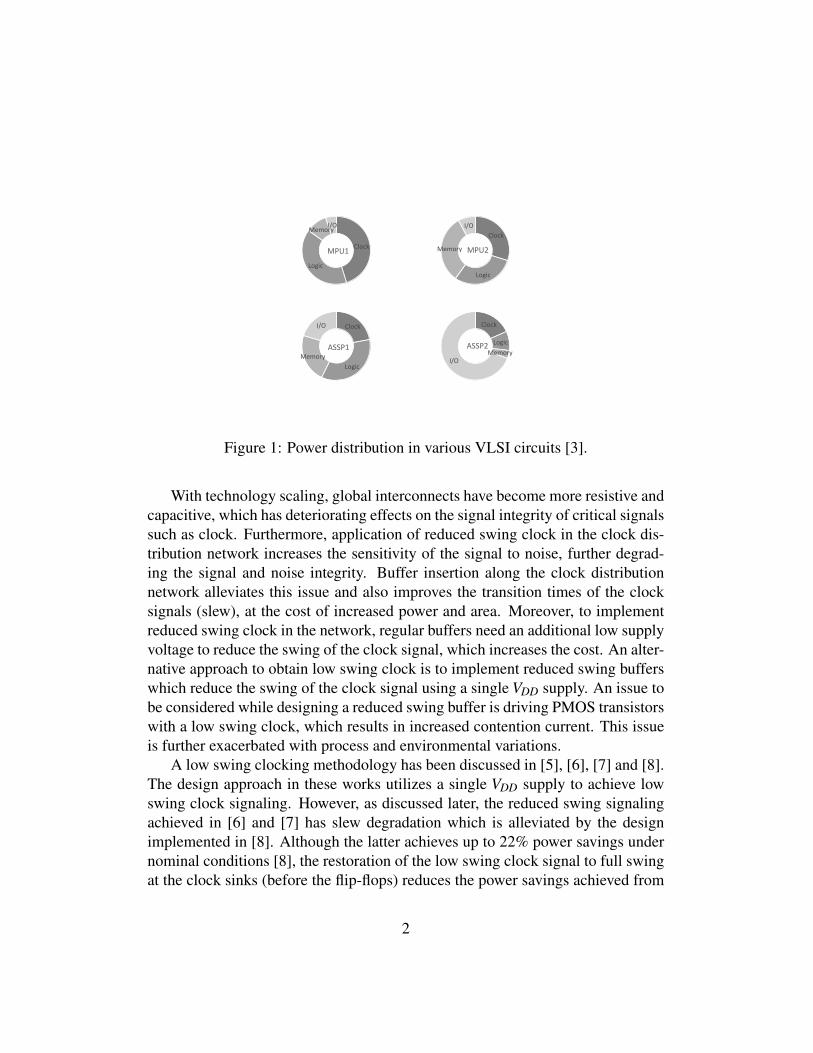
To improve the global performance and satisfy on-chip timing constraints,there is an increase in the number of pipeline registers, which has increased theoverall clock frequency to multi-gigahertz levels. Since all of the registers simul-taneously switch with each clock edge, significant power is dissipated in clockdistribution networks. According to [3], a clock distribution network can be re-sponsible for 20-45% of the total power consumption on-chip (Fig. 1), out ofwhich 90% of the power is dissipated at the leaves (last stage of interconnects andflip-flops) of the network.
Overall dynamic power dissipation to charge-discharge a load capacitance is
P = αCloadV 2DD f , (1)
where α is the activity factor (which is equal to one if the signal is clock), Cload isthe total switching capacitance, VDD is the supply voltage and f is the frequency.Based on this equation, one of the approaches to reduce power dissipation is toreduce the overall fan-out of the clock network, which is not a practical approachdue to higher integration levels. Another solution is to scale down the VDD supplyat the expense of performance degradation [4]. However, a considerably efficientsolution is to reduce the swing of the clock signal. Rewriting (1) to include theswing of a signal, Vswing,
P = αCloadVDDVswing f . (2)
From (2), a linear reduction in the clock swing can theoretically result in a lin-ear reduction in the overall dynamic power dissipation across a clock distributionnetwork.
1
Clock
Logic
MemoryI/O
MPU1
Clock
Logic
Memory
I/O
MPU2
Clock
Logic
Memory
I/O
ASSP1
Clock
Logic
MemoryI/O
ASSP2
Figure 1: Power distribution in various VLSI circuits [3].
With technology scaling, global interconnects have become more resistive andcapacitive, which has deteriorating effects on the signal integrity of critical signalssuch as clock. Furthermore, application of reduced swing clock in the clock dis-tribution network increases the sensitivity of the signal to noise, further degrad-ing the signal and noise integrity. Buffer insertion along the clock distributionnetwork alleviates this issue and also improves the transition times of the clocksignals (slew), at the cost of increased power and area. Moreover, to implementreduced swing clock in the network, regular buffers need an additional low supplyvoltage to reduce the swing of the clock signal, which increases the cost. An alter-native approach to obtain low swing clock is to implement reduced swing bufferswhich reduce the swing of the clock signal using a single VDD supply. An issue tobe considered while designing a reduced swing buffer is driving PMOS transistorswith a low swing clock, which results in increased contention current. This issueis further exacerbated with process and environmental variations.
A low swing clocking methodology has been discussed in [5], [6], [7] and [8].The design approach in these works utilizes a single VDD supply to achieve lowswing clock signaling. However, as discussed later, the reduced swing signalingachieved in [6] and [7] has slew degradation which is alleviated by the designimplemented in [8]. Although the latter achieves up to 22% power savings undernominal conditions [8], the restoration of the low swing clock signal to full swingat the clock sinks (before the flip-flops) reduces the power savings achieved from
2

low swing signaling throughout the clock distribution network.To overcome this issue, several papers discuss the design of low clock swing
based D flip-flops (DFF). The designs proposed in [9], [3], [10] and [11] imple-ment clocked PMOS transistors in the DFF which creates reliability issues whendriven by a low swing clock signal. This issue is alleviated in [12] which replacesthe transmission gates in the conventional flip-flop with NMOS passgates. TheDFF design proposed in this project has a similar approach, but achieves betterperformance and robustness as compared to other designs.
The rest of the dissertation is organized as follows. Chapter 2 discusses andanalyzes the reduced swing buffers for low swing clocking. Chapter 3 analyzesthe existing reduced swing clock based DFF topologies while proposing a novellow clock swing DFF architecture. The effect of the reduced swing buffer designand proposed DFF topology in low swing clock distribution network is discussedin Chapter 4 by driving the proposed low swing DFF with the reduced swingbuffers. The thesis is concluded in Chapter 5.
3

2 Custom Clock Buffer Design for Low Swing Op-eration
On-chip clock signal has high switching activity among other global signals andcan be responsible for up to 50% of the overall dynamic power consumption dueto large clock network capacitance [1]. A practical approach to alleviate this issueis to reduce the swing of active on-chip signals, such as clock [6]. To improvesignal and noise integrity, buffers are inserted along the clock distribution networkat regular intervals. Traditionally, for full swing clocks, conventional buffers areused in the clock distribution network, but for low swing clock signaling, thesefull swing buffers should be replaced by reduced swing buffers. Based on thelocation and function, the reduced swing buffers are of three types [8]:
1. Full swing to reduced swing buffer (FS-RS)
2. Reduced swing to reduced swing buffer (RS-RS)
3. Reduced swing to full swing buffer (RS-FS)
While the FS-RS buffer is inserted at the clock source, i.e., the root of the clocktree, to reduce the swing of the incoming full swing clock signal, the RS-RSbuffer is inserted throughout the clock distribution network to improve the signalintegrity of the low swing clock signal and satisfy slew constraints. The RS-FSbuffer is inserted at the leaves of the network to drive the leaf cells (flip-flops)operating at full VDD [8]. However, converting the low swing clock signal to fullswing at the leaf cells sacrifices the power savings achieved with low swing clocksignaling since most of the clocking power is consumed in the last stage of a clockdistribution network. Thus, it is critical to drive the leaf cells with a low swingclock signal, as achieved in this thesis by introducing a novel low swing DFF (seeChapter 3).
Various buffer architectures have been proposed to accomplish on-chip re-duced swing clock distribution, a few of which are discussed below. The primaryobjective, as mentioned previously, is to reduce the swing of the clock signal with-out using an additional supply voltage.
4

Section 2.1 provides an overview of existing reduced swing buffer topolo-gies. In this project, these existing designs are topologically modified to satisfythe required design constraints. These modifications are discussed in Section 2.2.The simulation results of the modified buffers are analyzed in Section 2.3. Therobustness is also evaluated for different process technologies and environmen-tal variations. Finally, the reliability of the reduced swing buffer architectures isinvestigated by introducing variations to the buffer load and input clock slew.
2.1 Existing Reduced Swing BuffersThe effectiveness and robustness of low swing signaling have been discussedin [6]. The reduced swing buffer used to obtain low swing signal in the networkis shown in Fig. 2. The two inverters driving the NMOS transistors prevent con-tention and provide a charge-discharge path for the output load capacitance. TheNMOS transistor connected to VDD is incapable of transmitting a strong logic-1. This buffer architecture, therefore, reduces the swing of the signal based onthe threshold voltage drop across the NMOS transistor (N1). The clock swing is,therefore, controlled by sizing the transistor, while considering the fan-out of thebuffer.
CLK X
CLKlow
N1
N2
Figure 2: Reduced swing buffer [6].
Another reduced swing buffer design is proposed in [7], which utilizes a diode-connected PMOS and NMOS (Fig. 3) to reduce the swing of the clock signal from(0 to VDD) to (Vtn to VDD− |Vt p|). Similar to [6], this design also obtains lowswing clock based on the threshold voltage drop across diode-connected PMOSand NMOS transistors.
The dependence of the swing level on the threshold voltage of a transistoraffects the reliability and integrity of the clock signal due to process variations.More importantly, there is a significant increase in the clock slew which has moredeteriorating effects when considering process, voltage and temperature (PVT)
5

N1
N2
P1
P2
CLK CLKlow
Figure 3: Reduced swing buffer with diode-connected transistors [7].
variations. Another design proposed in [8] removes this dependence on thresholdvoltage of the device by utilizing a delay produced by a delay chain to reduce theswing of the clock signal to a desired level (Fig. 4). As shown in this figure, theoutput of the inverter at the input stage is provided to the delay chain as well as theoutput inverter stage, i.e., N2 and P2. This delay chain provides a sufficient timewindow between signals X and Y during which the output is allowed to transitionto a desired level. Outside this time window, the transistors N3 and P3 are turnedoff at, respectively, VL and VH , such that VL > 0 and VH < VDD. Thus, a reducedswing clock is obtained at the output. The swing of the clock signal depends onthe delay time provided by the delay chain, the load capacitance of the buffer, andthe output current of the last stage.
2.2 Modified Reduced Swing BuffersThe buffers discussed previously are modified to obtain the desired reduction inclock swing (reduced VDD while maintaining the same VSS). The buffer designused for low swing clock signaling in [7] (Fig. 3) is slightly modified by removingthe diode-connected NMOS (Fig. 5) so as to reduce the swing of the clock from 0to (VDD−|Vt p|).
Similarly, the buffer design proposed in [8] is modified as shown in Fig. 6 byremoving the NMOS transistor, N3, at the output stage of the buffer. The clockswing is, therefore, reduced from 0 to VH instead of VL to VH , where VL > 0 andVH <VDD.
6

N1
N2
P1
P2
CLKlow
CLK X
X
Y
Y
Y
DELAY CHAIN
INPUT STAGE
OUTPUT STAGE
N3
P3
Figure 4: Delay chain based reduced swing buffer [8].
N1
P1
P2
CLKlowCLK
Figure 5: Modified version of the reduced swing buffer with diode-connectedtransistor.
7

N1
N2
P1
P2
CLKlow
CLK X
X
Y
Y
DELAY CHAIN
INPUT STAGE
OUTPUT STAGE
P3
Figure 6: Modified version of the delay chain based reduced swing buffer used inthis project.
Despite the advantage of reduced power consumption, a major drawback isthe flow of large contention current while driving the input stage with a reducedswing clock signal since the PMOS transistors driven by low swing clock signal isnot completely turned off. This issue can be alleviated by multi-threshold devicesin the buffer architecture. For example, the threshold voltage of the transistorsdriven by low swing clock signal can be increased by using high Vth transistors.The contention current can also be reduced to approximately 50% with a slightincrease in the channel length of the transistor. Specifically, from the simulationresults, it is observed that the leakage power is significantly reduced by increasingthe channel length of one of the transistors (PMOS or NMOS) at the input stageinverter of the reduced swing buffer. This technique reduces the leakage current by8.7% and 97%, respectively, for FS-RS and RS-RS buffer. In the design proposed,the length of the PMOS transistors at the input, P1, and within the delay chain isincreased by, respectively, 2x and 1.4x. These changes are determined based onthe clock slew requirement which should be less than 100ps, i.e., approximately15% of the clock period.
2.3 Simulation ResultsThe reduced swing buffers discussed in the previous section are designed in Ca-dence using 1V 45nm NCSU technology, which relies on predictive technology
8

models [13]. The clock frequency considered during the analysis is 1.5GHz withan input transition time of 10ps. The devices used in the design have nominalthreshold voltages to ensure sufficient reliability during multi-corner analysis. Inorder to replicate the large fan-out of the buffers in a typical clock distribution net-work, the transistors in the buffers are sized to drive a load capacitance of 50fF.The buffers are designed to obtain approximately 30% reduction in the clock volt-age swing at the output for both full swing to reduced swing (FS-RS) and reducedswing to reduced swing (RS-RS) operation.
The reduced swing buffer architecture in [6] reduces the swing of the clocksignal based on the threshold voltage of the NMOS transistor N1. Therefore, todrive a large load of 50fF and obtain a 30% reduction in the clock swing, thesize of the transistor should be increased to at least 70µm, which is significantlylarge for a 45nm technology. The inverter driving this transistor is also sizedaccordingly. The reduction in the clock swing as obtained from the simulationresults is shown in Fig. 7.
INPUT
OUTPUT
(a)
INPUT
OUTPUT
(b)
Figure 7: Reduced swing buffer [6]: (a) FS-RS simulation, (b) RS-RS simulation.
Another buffer architecture proposed in [7] also reduces the swing of the clocksignal using threshold voltage drop across the diode-connected PMOS and NMOStransistors. As discussed previously, the design is modified to obtain the desiredrange of output clock voltage swing (Fig. 5). This buffer architecture provides a30% reduction in the clock voltage swing with transistor sizes ranging between20-40µm, which is still significantly large. Furthermore, the clock slew and thedelay between input and output are significantly degraded due to diode-connectedtransistors, particularly during the low-to-high transition of the clock signal. This
9

behavior requires careful sizing of the transistors. The simulation results for theFS-RS and RS-RS operation of this buffer architecture are shown in Fig. 8.
INPUT
OUTPUT
(a)
INPUT
OUTPUT
(b)
Figure 8: Reduced swing buffer with diode-connected PMOS [7]: (a) FS-RS sim-ulation, (b) RS-RS simulation.
The buffer architecture proposed in [8] alleviates these issues resulting fromthe dependence of the output clock swing on the threshold voltage. This designutilizes a delay chain driven transistor at the output instead of a diode-connectedtransistor. The delay chain provides a time window which determines the outputvoltage swing of the clock. Due to sufficient clock slew at the output, this designpermits increasing the channel length of the low swing clock driven transistor toreduce the overall leakage power. The maximum transistor width does not exceed2µm while driving a load of 50fF, which is significantly smaller as compared tothe other reduced swing buffers. The reduction in the clock swing at the output isobtained, as shown in the simulation results in Fig. 9.
Section 2.3.1 provides a comparative analysis of these buffers in terms ofpower, delay and slew. To verify the functionality of the designs, the RS-RSbuffer is driven by FS-RS buffer to represent the connections within a clock tree.This analysis is presented in Section 2.3.2. The robustness of delay chain basedreduced swing buffer to PVT variations is analyzed in Section 2.3.3. The relia-bility of the buffer is also evaluated for different fan-outs and input clock slew inSection 2.3.4.
10

INPUT
OUTPUT
(a)
INPUT
OUTPUT
(b)
Figure 9: Delay chain based reduced swing buffer [8]: (a) FS-RS simulation, (b)RS-RS simulation.
2.3.1 Comparative analysis
The buffers discussed previously are compared with a conventional full swingbuffer in terms of dynamic power consumption, leakage power, average delay be-tween the input and output of the buffer, and the clock slew obtained at the output.The conventional buffer consists of two inverters and is sized to drive the sameload capacitance (50fF). Considering the input clock frequency and slew to be1.5GHz and 10ps respectively, Table 1 lists the data obtained from the simulationof reduced swing buffers. It should be noted here that the leakage power is aver-aged for high and low static values of the input clock. Similarly, the output slew isaveraged for both the low-to-high and high-to-low transitions of the clock signal.
Full swing to reduced swing buffer - Considering the FS-RS operation ofthe buffers [Table 1], the performance of [6] and [7] is degraded considerably incomparison to the conventional buffer. For the delay chain based buffer, despite anincrease in the leakage power by approximately 21%, the overall dynamic powerconsumption and the clock slew at the output are reduced, respectively, by 13.15%and 7.82%, in comparison with the conventional buffer. Furthermore, despite anincrease in the number of transistors in the buffer design, the average delay of thebuffer is increased by a negligible amount of 867fs, which is comparable to thatof the conventional buffer.
11

Tabl
e1:
Sim
ulat
ion
resu
ltsfo
rcon
vent
iona
lbuf
fera
ndre
duce
dsw
ing
buff
ers,
cons
ider
ing
both
FS-R
San
dR
S-R
Sop
erat
ion. Pa
ram
eter
sC
onve
ntio
nal
buff
er
Red
uced
swin
gbu
ffer
[6]
Red
uced
swin
gbu
ffer
with
diod
e-co
nnec
ted
PMO
S[7
]
Del
aych
ain
base
dre
duce
dsw
ing
buff
er[8
]
FS-R
SR
S-R
SFS
-RS
RS-
RS
FS-R
SR
S-R
SV o
ut(m
V)
1000
698.
9369
3.96
700.
3169
9.01
701.
3770
0.76
Dyn
amic
pow
er(µ
W)
78.8
314
5.6
148.
830
130
0.4
68.4
668
.31
Aver
age
dela
y(p
s)49
.271
76.5
596
.001
102.
208
129.
593
50.1
3854
.892
Out
puts
lew
(ps)
58.6
1762
.154
66.5
3365
.524
65.9
2754
.033
54.7
11L
eaka
gepo
wer
(nW
)22
.85
411.
0215
7725
770
56.5
27.6
9525
0.19
12

Reduced swing to reduced swing buffer - For RS-RS operation, low swingclock signal (0-700mV) is applied at the input of the reduced swing buffers. Theleakage power for the buffers in [6] and [7] increases by approximately 69x and308x, respectively, as compared to the conventional buffer. Increase in leakagepower is exacerbated when analyzing the circuit at the PVT corners, making thesecircuits less robust. The delay chain based reduced swing buffer also exhibits 11xincrease in the leakage power, which is primarily due to the contention currentflow at the input inverter, where a PMOS transistor driven by a low swing clocksignal is not completely turned off. This leakage current is obtained after increas-ing the channel length of the clock-driven PMOS transistor by 2x. Despite thehigh leakage power, the dynamic power dissipation and the output clock slew arereduced, respectively, by 15.4% and 6.7% as compared to the conventional fullswing buffer. These values are comparable to the FS-RS operation of the samebuffer design. Contrary to the average delay obtained during the FS-RS operationof the buffer, there is approximately 11% increase in the delay across the RS-RSbuffer in comparison to the conventional full swing buffer.
2.3.2 Full swing to reduced swing buffer driving reduced swing to reducedswing buffer
In the clock tree design, the full swing clock signal generated by the clock source,i.e., phase-locked loop (PLL), is converted to a reduced swing clock signal by theFS-RS buffer which then drives the RS-RS buffer. To represent this behavior andensure correct functionality of the design, FS-RS buffer is used to drive a RS-RSbuffer which further drives a load of 50fF. Since the FS-RS buffer drives only oneRS-RS buffer, the design is slightly modified to accommodate this small fan-outby decreasing the number of inverters in the delay chain to 3 and downsizing thetransistors at the output stage of the buffer. Using a similar clock frequency andslew, the design is simulated, as shown in Fig. 10.
It is shown in this figure that the desired reduced swing is obtained and main-tained at the output of both buffers. There is an increase in the delay and power,as expected. To calculate the leakage power, piecewise-linear input is provided asthe input to model the clock gating functionality, and the leakage power is ana-lyzed over the simulation period when the clock is gated. This is required, becausewhen the input clock is at logic-1, the output of the FS-RS buffer does not exceed400mV, which results in excessive amount of leakage at the input of the RS-RSbuffer. It is to be noted that the output slew and average delay are averaged forthe low-to-high and high-to-low transitions of the signal. Similarly, the leakage
13

INPUT
FS-RS OUTPUT
RS-RS OUTPUT
Figure 10: FS-RS buffer driving a RS-RS buffer, which drives a 50fF load.
power is also averaged for low and high static input values.
Table 2: Simulation results of FS-RS buffer driving a RS-RS buffer, which drivesa load of 50fF.
Parameter FS-RS buffer RS-RS bufferVout (mV) 699.9 700.2
Output Slew (ps) 17.1 54.6Average delay (ps) 21.7 77.3
Dynamic power (µW) 79.48Leakage power (nW) 367.8
2.3.3 Robustness to PVT variations
A critical challenge in nanoscale ICs is the variations incurred during fabricationand fluctuations in operating voltage and temperature [1]. The delay chain basedreduced swing buffer is simulated and analyzed for different process corners, op-erating voltage and temperature (PVT) variations. It is important to analyze therobustness and reliability of the design for varying PVT conditions, particularly atthe fast and slow corners.
Due to an increase in the threshold voltage of the transistors, the slow corneris considered for the worst-case delay analysis. On the contrary, fast corner isconsidered for the dynamic power and leakage power analysis due to decrease in
14

the threshold voltage of the devices. Furthermore, the operating voltage of thebuffer design is decreased and increased by 10% for, respectively, slow and fastcorners, to consider voltage variations.
The threshold voltage of the transistors exhibits almost a linear dependence ontemperature such that there is a reduction in the threshold voltage of the transistoras the operating temperature of the circuit is increased [14]. This relationship canbe approximated by
Vt(T ) =Vt(Tr)− kvt(T −Tr), (3)
where T is the absolute temperature, Tr is the room temperature and kvt is approx-imately 1-2 mV/K [14]. On the contrary, the carrier mobility of the transistorsdecreases with increasing temperature according to the relation,
µ(T ) = µ(Tr)(TTr)−kµ (4)
where kµ is a fitting parameter approximately equal to 1.5 [14]. It is observed thatthe increase in mobility is more effective at lower temperatures due to which theworst-case delay and slew are analyzed at high temperature (165◦C). However,due to reduced feature size, the threshold voltage variation at lower temperaturescannot be neglected. Therefore, the circuit is simulated at both high and lowtemperatures for the worst-case dynamic power analysis.
The process and voltage corners for leakage power analysis is similar to thatconsidered for dynamic power analysis. From [14], the current driving capabilityof a transistor with variations in temperature depends on VGS of the transistor,according to which the transistor shows an exponential decrease in current whenVGS drops below the threshold voltage level. This exponential decrease is the sub-
Vgs
√Ids
IncreasingTemperature
Figure 11: I-V characteristics of NMOS with varying temperature [14].
15

Table 3: Worst-case corner simulation results for conventional buffer and delaychain based reduced swing buffer.
PVT corner Parameter Conventionalbuffer
Delay chain basedreduced swing buffer
FS-RS RS-RSFS-RSdrivingRS-RS
SS, 0.9V, 165◦CDelay (ps) 139.7 180.8 197.0 286.2
OutputSlew (ps)
183.6 187.8 187.5 184.9
FF, 1.1V, 165◦C
DynamicPower(µW)
98.3 90.3 92.9 106.4
LeakagePower(µW)
1.6 1.1 5.3 3.6
threshold leakage current which increases with increasing temperature, as shownin Fig. 11. Therefore, the operating temperature considered for leakage poweranalysis of the designs is 165◦C.
The worst-case analysis results of the delay chain based reduced swing bufferand the conventional buffer are summarized in Table 3. In comparison to the con-ventional buffer, the delay chain based reduced swing buffer exhibits an increasein the average delay. The slew and dynamic power consumption, however, arealmost comparable to that of the conventional buffer. The leakage power for theFS-RS buffer is observed to be less than the conventional buffer, while there isan increase in the leakage power when a reduced swing clock is used to drive thebuffer.
2.3.4 Robustness to buffer load and clock slew variations
All of the simulation results in the previous sections are obtained consideringan input clock slew of 10ps and buffer output load of 50fF. While analyzing thebuffer design at the worst case corners, it is observed that the clock slew at thebuffer output can increase to approximately 190ps, which drives RS-RS buffers.The buffers should therefore operate reliably for input slew as high as 200ps. To
16
verify the robustness, the FS-RS and RS-RS buffers are analyzed for differentinput slews ranging from 40ps to 200ps. The simulation results obtained from theparametric analysis of the FS-RS and the RS-RS buffer for clock slew variationsare shown in Fig. 12. From the figure, it is shown that variation in input clockslew does not affect the output clock slew or the output voltage level (700mV).The output, however, shifts slightly with every increment in the input clock slewwhich is due to an increase in the transition times of the input clock signal.
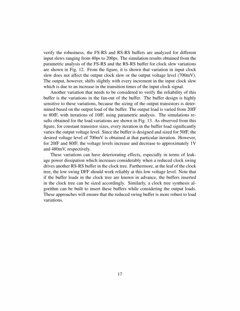
Another variation that needs to be considered to verify the reliability of thisbuffer is the variations in the fan-out of the buffer. The buffer design is highlysensitive to these variations, because the sizing of the output transistors is deter-mined based on the output load of the buffer. The output load is varied from 20fFto 80fF, with iterations of 10fF, using parametric analysis. The simulations re-sults obtained for the load variations are shown in Fig. 13. As observed from thisfigure, for constant transistor sizes, every iteration in the buffer load significantlyvaries the output voltage level. Since the buffer is designed and sized for 50fF, thedesired voltage level of 700mV is obtained at that particular iteration. However,for 20fF and 80fF, the voltage levels increase and decrease to approximately 1Vand 480mV, respectively.
These variations can have deteriorating effects, especially in terms of leak-age power dissipation which increases considerably when a reduced clock swingdrives another RS-RS buffer in the clock tree. Furthermore, at the leaf of the clocktree, the low swing DFF should work reliably at this low voltage level. Note thatif the buffer loads in the clock tree are known in advance, the buffers insertedin the clock tree can be sized accordingly. Similarly, a clock tree synthesis al-gorithm can be built to insert these buffers while considering the output loads.These approaches will ensure that the reduced swing buffer is more robust to loadvariations.
17

(a)
(b)
Figure 12: Delay chain based reduced swing buffer parametric analysis with vari-able clock slew: (a) FS-RS simulation, (b) RS-RS simulation.
18

(a)
(b)
Figure 13: Delay chain based reduced swing buffer parametric analysis with vari-able buffer load: (a) FS-RS simulation, (b) RS-RS simulation.
19

3 Custom D Flip-Flop Design for Low Swing Oper-ation
As described in the previous chapter, clock distribution network is a primarysource of on-chip power consumption. Clock networks consume 20-45% of totalon-chip power [3]. This power dissipation is the result of increased pipelining inthe design which has led to an increase in the number of flip-flops and therefore,the total interconnect length of the clock network [15]. Approximately 90% of theclock power is consumed by the flip-flops and last branches of a clock tree [3]. It istherefore critical to drive the sink flip-flops with a low swing clock signal to max-imize the power savings. Various D flip-flop (DFF) architectures are discussed inthis chapter which can work efficiently when driven by a low swing clock signal.If a conventional full swing flip-flop is used in low swing operation, the PMOStransistors driven by low swing clock signal are not completely turned off. Thisbehavior results in robustness and reliability issues as the transmission gates failto maintain the logic-0 level, producing a glitch of approximately 380mV. Thereis also a 15% increase in clock-to-Q delay when a reduced swing clock is used todrive the conventional full swing flip-flop, which is exacerbated at the worst-casecorners.
Section 3.1 provides an overview of the current low clock swing DFF topolo-gies. It is followed by the proposal of a novel DFF topology in Section 3.2. Acomparative analysis of the DFF architectures is provided in Section 3.3.
3.1 Low Clock Swing D Flip-Flop DesignWith reducing feature size, minimizing the leakage current has become a sig-nificant issue towards achieving low power design in addition to lowering theclock voltage swing and reducing the charge-discharge capacitance [9]. A lowswing clock topology based on clocked CMOS (C2MOS) and sense amplifier(SA) is proposed in [9] (L C2MOS SA, Fig. 14a). This design reduces the charge-discharge capacitance and implements a conditional pre-charge and dischargetechnique to achieve low power consumption. The design is area efficient anda considerable reduction in leakage is also obtained with this topology. How-
20

ever, although this design does not need an additional supply voltage for the clocksub-circuit, the use of diode-connected PMOS to reduce the clock swing is notan efficient approach as it significantly increases the low-to-high transition timeof the low swing clock. This approach also considerably affects the robustnessand reliability of the circuit at the worst-case corner. Another issue is the need offull swing clock signal at the slave stage of the DFF which defies our objective ofusing a low swing clock signal in the DFF.
Another topology, reduced clock swing flip-flop (RCSFF, Fig. 14b), proposedin [3], uses single low swing clock for the DFF operation. This topology uses anadditional low voltage supply, VDDL (700 mV) in the clock sub-circuit to providelow swing clock to the respective transistors in the design. The clock sub-circuitused for this circuit is shown in Fig. 15. However, when the clock signal goeshigh (VDDL <VDD), the PMOS transistors are not completely turned off, resultingin large leakage current. To fix this issue, the design uses an additional voltagesupply to connect the well of the clocked PMOS transistors at a higher voltage biasthan the supply voltage, thereby increasing the threshold voltage of the clockedtransistors. An additional well increases the design area as well as the complexityof the design.
A NAND-type keeper flip-flop design proposed in [10] (NDKFF, Fig. 14c),does not require a separate well, but it causes excessive leakage current flowthrough transistors P2, N1-N3 when node X goes low. Also the level-keepingtransistors, i.e., P2, N4, N5 and I1-I2, have a race condition when node X transi-tions from low to high, resulting in an increase in the transition time of the output.This effect is exacerbated during worst-case delay analysis of the design and canbe partially alleviated by carefully sizing the transistors.
Contention reduced flip-flop proposed in [11] (CRFF, Fig. 14d) utilizes apulsed clock signal to provide a short transparency window during which the out-put is discharged through the NMOS transistors N1-N4. During this transparencywindow, the clocked transistors P5 and P6 disconnect the CMOS latch (I1-I2) toprevent any contention current. Furthermore, transistors P1 and P2 are controlledby input D through P3 and P4 which further reduces contention. However, therestill remains the issue of completely turning off the PMOS transistor due to lowswing clock signal.
In all of the topologies discussed above, driving PMOS transistors with lowswing clock has been the primary issue resulting in large contention current flow.The DFF design provided in [12] alleviates this issue by using passgate NMOStransistors instead of transmission gates, as shown in Fig. 16. Due to the inefficienttransmission of logic-1 across the passgate transistor, a weak keeper PMOS tran-
21

QN Q
D
CLK
CLK
_CLK
_CLK
CLOCK
CLOCK
CLK
_CLK
N1
N2
N3
N4
N6
N7
N5
P1
P2
P3
P4
(a)
Vwell
CLK
CLK
CLK
D
Q QN
N1
N2
N5
N3
N4
N6
P1P2
P4P3
(b)
VDD_L
QN
N1
N2
N3
N6
N7
N8
N4N5
P1P2
P3
Q
X
(c)
D
VDD_L
_DD
DD
DD
_DD
CLK
Q
_Q
N1
N2
N3
N4
P1
P2
P3
P4
P5
P6
(d)
Figu
re14
:Low
swin
gD
FFar
chite
ctur
es:(
a)L
owcl
ock
swin
gC
2 MO
San
dse
nse
ampl
ifier
(SA
)(L
C2 M
OS
SA)
DFF
[9],
(b)
Red
uced
cloc
ksw
ing
flip-
flop
(RC
SFF)
[3],
(c)
NA
ND
-typ
eke
eper
DFF
(ND
KFF
)[1
0],
(d)
Con
-te
ntio
nre
duce
dfli
p-flo
p(C
RFF
)[11
].
22

CLOCK CLK _CLK
VDD_L
Figure 15: Clock sub-circuit used for DFF architectures RCSFF [3], NDKFF [10],CRFF [11], passgate DFF [12] and the proposed DFF in this thesis.
sistor is included in the design to pull-up node X and Y to VDD. Since no clockedPMOS transistors are used in this design, the total leakage power is considerablyreduced. However, there is still contention current flow through the transistors P2,N2, N1 and P4, N4, N3 in the corresponding master and slave latches during thehigh-to-low transition of the nodes X and Y, respectively. This contention currentcan be reduced to some extent by carefully sizing the respective transistors.
_CLK
X
_CLK
CLK
YD Q
KEEPER
N1
P1
N3
P3
N5
P5
N6
P6
N2 N4
P2 P4
CLKN8
N7
N10
N9
Figure 16: Passgate DFF for low swing clock signal [12].
23

3.2 Proposed Low Swing D Flip-FlopThe proposed DFF architecture, shown in Fig. 17, is similar to the conventionalfull swing DFF where the primary difference is the use of passgates instead oftransmission gates in the design. The clock sub-circuit used for this topologyis shown in Fig. 15. The idea of using passgates is similar to the DFF designpresented in [12], but there are some important differences, as shown in Fig. 17.Since there are no PMOS transistors driven by a low swing clock signal, the con-tention current is considerably reduced. However, NMOS passgate is incapableof pulling up the node Y to VDD. A keeper PMOS and pull-down logic consistingof two NMOS transistors are added to improve this transition. Another PMOStransistor controlled by input D is added to avoid contention current flow throughthe transistors P4, N2, N1 when the node Y transitions from VDD to GND. Sim-ilarly, node X is used to drive the transistor P7 in the slave mode. The sizing ofthe transistors and the use of multi-threshold devices in the design are exploitedto accomplish low power-delay characteristics and balance related trade-offs.
_CLK
CLK
Y
X
_CLK
CLK
_CLK
CLK
D
D
X
Q
KEEPER
PULL-DOWN LOGIC
N1
P1
N3
P2
N5
P3
N10
P8
N2 N4
P4 P5
P6 P7
N6
N7
N8
N9
N11
P9
N12
P10
N13N14
Figure 17: Proposed low swing DFF.
24

3.3 Simulation ResultsThe proposed DFF is designed along with L C2MOS SA [9], RCSFF [3], ND-KFF [10], CRFF [11] and passgate DFF [12] topologies using 1V 45nm NCSUtechnology. The clock and data frequencies considered for these simulations are,respectively, 1.5 GHz and 150 MHz. The input clock slew is 10ps. For fair com-parison, the transistors in each design are sized to obtain a CLK-to-Q delay in therange of 65-70ps for a fan-out of 5fF. High Vth and low Vth transistors are alsoused in the designs to accommodate the power-delay trade-off. Both NDKFF andCRFF use pulsed low swing clock signal which should be long enough to ensureproper functionality. To achieve a fair comparison, for all of the DFF architec-tures, the swing of the clock signal is reduced by using an additional low supplyvoltage of 700mV, which is used as VDDL for the inverter chain. The output of thisinverter chain drives the clocked transistors in the flip-flop. The L C2MOS SAdesign as mentioned in [9] drives the slave stage with a full swing clock and theclock sub-circuit uses a diode connected PMOS to reduce the clock swing. Tocompare with other low swing clock driven DFF topologies, the same topology ismodified by integrating low swing clock for the slave stage and using an additionallow supply voltage in the clock sub-circuit.
Section 3.3.1 compares the simulation results of the DFF architectures dis-cussed in the previous chapter. The reliability of the DFF topologies is verifiedfor different clock voltage swings in Section 3.3.2. The robustness of the proposedDFF design is analyzed for PVT variations in Section 3.3.3.
3.3.1 Comparative analysis
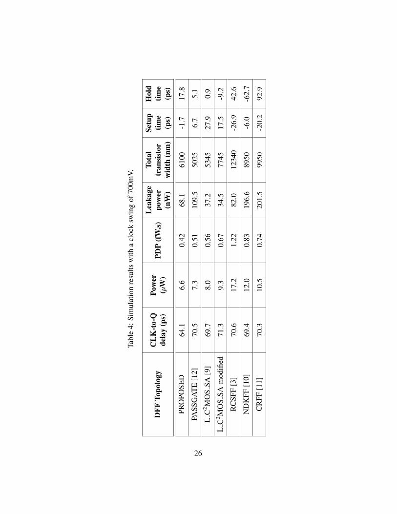
Assuming the clock swing is 700mV, a comparative analysis of the DFF architec-tures is achieved. The results are listed in Table 4. The leakage power is averagedfor the leakage values obtained while considering four possible non-transitionalcombinations of data and clock signals. From the table, it is shown that althoughthe leakage power for L C2MOS SA [9] is approximately half of the leakage ofthe proposed topology, the overall dynamic power and power-delay product (PDP)of the proposed topology exhibit an average improvement of 33.6% and 39.5%,respectively. Furthermore, comparing the proposed DFF design with [12], the pro-posed architecture provides a considerable improvement in performance in termsof PDP and leakage power. A rough estimate of the area is obtained by comparingthe total width of PMOS and NMOS transistors in the designs. As listed in Table4, the proposed topology achieves less area than modified version of [9], [3], [10]
25
Tabl
e4:
Sim
ulat
ion
resu
ltsw
itha
cloc
ksw
ing
of70
0mV.
DFF
Topo
logy
CL
K-t
o-Q
dela
y(p
s)Po
wer
(µW
)PD
P(f
W.s)
Lea
kage
pow
er(n
W)
Tota
ltr
ansi
stor
wid
th(n
m)
Setu
ptim
e(p
s)
Hol
dtim
e(p
s)
PRO
POSE
D64
.16.
60.
4268
.161
00-1
.717
.8
PASS
GA
TE
[12]
70.5
7.3
0.51
109.
550
256.
75.
1
LC
2 MO
SSA
[9]
69.7
8.0
0.56
37.2
5345
27.9
0.9
LC
2 MO
SSA
-mod
ified
71.3
9.3
0.67
34.5
7745
17.5
-9.2
RC
SFF
[3]
70.6
17.2
1.22
82.0
1234
0-2
6.9
42.6
ND
KFF
[10]
69.4
12.0
0.83
196.
689
50-6
.0-6
2.7
CR
FF[1
1]70
.310
.50.
7420
1.5
9950
-20.
292
.9
26
and [11]. It is also observed that although the proposed topology does not exhibitthe minimum values of setup-hold time, they are still reasonably low to support areliable operation [16], [17].
3.3.2 Response to different clock swings
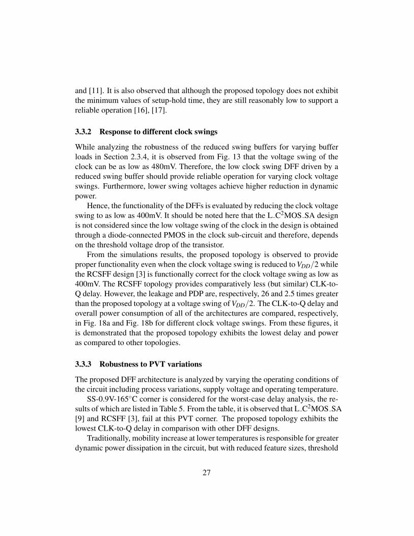
While analyzing the robustness of the reduced swing buffers for varying bufferloads in Section 2.3.4, it is observed from Fig. 13 that the voltage swing of theclock can be as low as 480mV. Therefore, the low clock swing DFF driven by areduced swing buffer should provide reliable operation for varying clock voltageswings. Furthermore, lower swing voltages achieve higher reduction in dynamicpower.
Hence, the functionality of the DFFs is evaluated by reducing the clock voltageswing to as low as 400mV. It should be noted here that the L C2MOS SA designis not considered since the low voltage swing of the clock in the design is obtainedthrough a diode-connected PMOS in the clock sub-circuit and therefore, dependson the threshold voltage drop of the transistor.
From the simulations results, the proposed topology is observed to provideproper functionality even when the clock voltage swing is reduced to VDD/2 whilethe RCSFF design [3] is functionally correct for the clock voltage swing as low as400mV. The RCSFF topology provides comparatively less (but similar) CLK-to-Q delay. However, the leakage and PDP are, respectively, 26 and 2.5 times greaterthan the proposed topology at a voltage swing of VDD/2. The CLK-to-Q delay andoverall power consumption of all of the architectures are compared, respectively,in Fig. 18a and Fig. 18b for different clock voltage swings. From these figures, itis demonstrated that the proposed topology exhibits the lowest delay and poweras compared to other topologies.
3.3.3 Robustness to PVT variations
The proposed DFF architecture is analyzed by varying the operating conditions ofthe circuit including process variations, supply voltage and operating temperature.
SS-0.9V-165◦C corner is considered for the worst-case delay analysis, the re-sults of which are listed in Table 5. From the table, it is observed that L C2MOS SA[9] and RCSFF [3], fail at this PVT corner. The proposed topology exhibits thelowest CLK-to-Q delay in comparison with other DFF designs.
Traditionally, mobility increase at lower temperatures is responsible for greaterdynamic power dissipation in the circuit, but with reduced feature sizes, threshold
27

0.4
0.5
0.6
0.7
0.8
50100
150
200
250
300
Clo
ck v
olta
ge s
win
g (V
)
Clock−to−Q delay (ps)
PR
OP
OS
ED
L−C
2 MO
S−
SA
−2
RC
SF
FN
DK
FF
CR
FF
(a)
0.4
0.5
0.6
0.7
0.8
68101214161820
Clo
ck v
olta
ge s
win
g (V
)
Power dissipation (µW)
PR
OP
OS
ED
L−C
2 MO
S−
SA
−2
RC
SF
FN
DK
FF
CR
FF
(b)
Figu
re18
:Res
pons
eof
DFF
sto
diff
eren
tclo
cksw
ings
:(a)
CL
K-t
o-Q
dela
y(p
s)vs
cloc
kvo
ltage
swin
g(m
V),
(b)
Tota
lpow
erdi
ssip
atio
n(µ
W)v
scl
ock
volta
gesw
ing
(mV
).
28

Table 5: Worst-case corner analysis of the proposed DFF.
DFF TopologyCLK-to-Q delay
(ps) atSS-0.9V-165◦C
Dynamic power(µW) at FF-1.1V
Leakage power(µW) at
FF-1.1V-165◦C
PROPOSED 150.8 8.9 (T=-40◦C) 1.1
PASSGATE [12] 160.7 11.0 (T=165◦C) 1.7
L C2MOS SA [9] FAIL 10.8 (T=165◦C) 0.6
L C2MOS SA-modified
178.8 11.3 (T=165◦C) 0.6
RCSFF [3] FAIL 21.5 (T=-40◦C) 1.5
NDKFF [10] 210.0 17.2 (T=165◦C) 2.5
CRFF [11] 175.7 17.7 (T=165◦C) 3.8
voltage variations due to temperature fluctuations cannot be neglected. The DFFdesigns are, therefore, simulated for both low and high operating temperaturesto analyze the overall dynamic power dissipation in the circuit. A 10% increasein supply voltage is also considered. The dynamic power analysis results at FF-1.1V corner are listed in Table 5. The proposed DFF provides comparatively lowdynamic power dissipation at the PVT corner considered for this analysis.
From Fig. 11, it is observed that the sub-threshold current increases with anincrease in temperature. Thus, the FF-1.1V-165◦C corner is considered for worst-case analysis of the leakage power. The leakage power obtained is averaged overfour possible logic-0 and logic-1 iterations of the input data and clock signals.From the table it is shown that the proposed topology exhibits approximately twicethe leakage power as compared to L C2MOS SA design [9], which is similar tothe results obtained when simulated in typical PVT corner (Table 4). However,the L C2MOS SA design [9] fails during the worst-case delay analysis at SS-0.9V-165◦C corner.
29

4 Low Swing Clock Distribution Network
The reduced swing buffer and low swing D flip-flop architectures discussed inthe previous chapters are designed and analyzed in a simplified low swing clockdistribution network. Section 2.3.2 discusses the operation of RS-RS buffer whendriven by FS-RS buffer. To complete the clock distribution network, the RS-RS buffer is used to drive the proposed DFF architecture, as shown in Fig. 19.Traditionally, each buffer in the clock tree has a large fan-out due to which the
50 DFFs
FS-RS RS-RS
RS-RS
CLK
_CLK
D
CLK_FS-RSCLK_IN
Figure 19: Simplified low swing clock distribution network.
RS-RS buffer is used to drive 50 DFFs. Each DFF drives an individual load of5fF. Since a DFF requires two low swing clock signals CLK and CLK, the FS-RSbuffer is used to drive two RS-RS buffers to generate opposite phase clock signals.Note that the circuit utilizes a single power supply voltage of 1V. The simulationresults for the low swing clock distribution network are presented in Section 4.1.The robustness to environmental variations is discussed in Section 4.2.
4.1 Simulation ResultsThe clock distribution network is designed in Cadence using 1V 45nm NCSUtechnology considering 1.5GHz clock frequency and 10ps input clock slew. Thedata frequency considered for each DFF in the network is 150MHz. Fig. 20 showsthe simulation results obtained for the low swing clock distribution network. Asshown in this figure, the output of the RS-RS buffer varies with the transitions ininput D due to high sensitivity to load variations (Fig. 13). The gate capacitance
30

Figure 20: Simulation results of a simplified low swing clock distribution network.
of the clocked NMOS transistors varies with voltage variations at the drain/sourceof the transistor, which is controlled by input D. This load sensitivity causes vari-ations in the clock swing. The simulation results of the clock distribution networkare listed in Table 6. According to the results, the clock swing driving the DFFsvaries by >100mV due to buffer load variations. Also note that, there is a skew of17ps between the clocks which is due to the additional inverter required in the RS-RS buffer to generate two out-of-phase clock signals. Moreover, the clock slewremains the same for the two clock signals. The buffer delay for each buffer ismeasured from the clock source and is averaged for both low-to-high and high-to-low transitions of the clock signals. Similarly, the leakage power is also averagedfor the four possible iterations of logic-0 and logic-1 for data and clock signals.
31

Table 6: Simulation results for a simplified low swing clock distribution network.
Parameter FS-RSBuffer
RS-RSBuffer(CLK)
RS-RSBuffer( CLK)
ProposedDFF
Voltage swing(mV)
698.6722.9-822.4
701-917.8 N/A
Clock slew(ps)
16.9 52.8 52.8 N/A
Buffer delay(ps)
21.7 83.4 100.1 N/A
CLK-to-Qdelay (ps)
N/A N/A N/A 130.8
Dynamicpower (µW)
336.6
Leakagepower (µW)
3.64
4.2 Robustness to PVT VariationsTo verify the reliability of the low swing clock distribution network, the design isanalyzed for different environmental and process variations. Similar to the previ-ous analyses discussed for the custom reduced swing buffers and proposed DFF,the worst-case corner for the delay and slew analysis is SS-0.9V-165◦C while thecorner considered for leakage and dynamic power analysis is FF-1.1V-165◦C. Thedesign is also evaluated for lower temperatures for the fast corner during poweranalysis since with reduced feature sizes, the threshold voltage variations shouldbe considered. Indeed, from the simulation results, it is observed that the worst-case dynamic power is obtained at the highest temperature. The delay and poweranalysis results are listed in Table 7. Note that the buffer delay and CLK-to-Qdelay are measured from the clock source and, averaged for low-to-high and high-to-low transitions. The results demonstrate a reliable operation of the low swingclock distribution network considering the large fan-out at the output of the RS-RSbuffers.
A primary concern is the sensitivity of the reduced swing buffer to load vari-
32

Table 7: Worst-case analysis of a simplified low swing clock distribution network.
PVTcorner Parameter FS-RS
Buffer
RS-RSBuffer(CLK)
RS-RSBuffer( CLK)
ProposedDFF
SS,0.9V,165◦C
Bufferdelay (ps)
61.8 436.2 835.7 N/A
Clock slew(ps)
49.1 161.1 157.4 N/A
CLK-to-Qdelay(ps)
N/A N/A N/A 358.3
FF,1.1V,165◦C
Dynamicpower(µW)
489.1
Leakagepower(µW)
56.15
ations as it degrades the robustness of the design. This issue can be alleviated bydesigning a DFF with constant input capacitance such as a tristate DFF.
Another issue is the routing complexity arising from distribution of two clocksignals for each DFF at the output of the RS-RS buffer. Since the two clock signalsare out-of-phase, signal and noise integrity are degraded. Besides, the routingcapacitance is also doubled in addition to an increase in area. This issue can bepartially alleviated by distributing a single low swing clock signal and generatingthe opposite phase clock inside the DFF architecture. This approach provides anarea overhead, but will reduce the routing complexity and hence, the capacitanceat the leaf of a clock distribution network.
33

5 Conclusions
The primary objective of this thesis is to reduce the swing of a clock signal alongthe distribution network using a single VDD supply. To accomplish this objec-tive, custom delay chain based reduced swing buffer architecture [8] is discussedand compared with other reduced swing buffers introduced in [6] and [7]. Forthe project, the buffers in [7] and [8] are topologically modified to obtain the de-sired reduced clock swing (0-700mV). Design solutions are also applied to reducethe leakage power. Low clock swing based D flip-flops are also analyzed whileproposing a novel low swing DFF architecture. All of the simulations are per-formed using 1V 45nm NCSU technology considering the clock frequency andinput slew of 1.5GHz and 10ps, respectively.
For a fan-out of 50fF, the delay chain based reduced swing buffer providesapproximately 14% and 7% improvement in, respectively, dynamic power dissi-pation and clock slew, with negligible increase in the buffer delay as comparedto the conventional buffer. This buffer is also analyzed for different process andenvironmental variations such as operating voltage and temperature. Although thedynamic power dissipation and clock slew at the output are reduced as comparedto the conventional buffer, the delay chain based reduced swing buffer exhibits anincrease in the buffer delay and leakage power. This buffer is also shown to beconsiderably reliable to input clock slew variations since the output voltage levelof the buffer is maintained at the desired 700mV with negligible variations in theoutput slew. This buffer, however, is sensitive to output load variations whichdrastically affects the output clock swing. This issue can be alleviated by pre-determining the fan-out of the buffer and accordingly sizing the transistors or bydesigning a low clock swing based DFF which can operate reliably at the clockvoltage swing as low as 500mV.
Various low clock swing DFF architectures have been previously proposed,which are discussed and analyzed. A novel low swing DFF design is also pro-posed. The data frequency considered for the simulations is 150MHz. The pro-posed DFF is an area efficient design with considerable improvement in the per-formance in terms of power and power-delay product, which are reduced by, re-spectively, 33.6% and 39.5%, as compared to other low swing DFFs. The pro-posed flip-flop is also analyzed for different clock swings. It is observed that the
34

proposed DFF operates reliably, with minimum PDP values, even if the clockvoltage swing is reduced to VDD/2. The robustness of the architectures is alsocompared considering PVT variations where the proposed design exhibits 19.34%and 38.91% average improvement in, respectively, CLK-to-Q delay and dynamicpower dissipation.
A simplified low swing clock distribution network is also analyzed by driving50 proposed DFFs with the reduced swing buffers. The simulation results demon-strate a robust design which is reliable at the worst-case corners. The limitation isarea overhead due to routing complexity at the leaf of the clock distribution net-work. This issue can be alleviated by modifying the DFF topology, which remainsas future work.
35

References[1] E. Salman and E. G. Friedman, High Performance Integrated Circuit Design.
McGraw-Hill, 2012.
[2] D. Liu and C. Svensson, “Power consumption estimation in CMOS VLSIchips,” Solid-State Circuits, IEEE Journal of, vol. 29, no. 6, pp. 663–670,1994.
[3] H. Kawaguchi and T. Sakurai, “A reduced clock-swing flip-flop (RCSFF) for63% power reduction,” Solid-State Circuits, IEEE Journal of, vol. 33, no. 5,pp. 807–811, 1998.
[4] R. Gonzalez, B. M. Gordon, and M. A. Horowitz, “Supply and thresholdvoltage scaling for low power CMOS,” Solid-State Circuits, IEEE Journalof, vol. 32, no. 8, pp. 1210–1216, 1997.
[5] D. Markovic, J. Tschanz, and V. De, “Feasibility study of low-swing clock-ing,” in Microelectronics, 2004, 24th International Conference, vol. 2,pp. 547–550.
[6] H. Zhang, V. George, and J. Rabaey, “Low-swing on-chip signaling tech-niques: effectiveness and robustness,” Very Large Scale Integration (VLSI)Systems, IEEE Transactions on, vol. 8, pp. 264–272, June 2000.
[7] J. Pangjun and S. Sapatnekar, “Low-power clock distribution using multiplevoltages and reduced swings,” Very Large Scale Integration (VLSI) Systems,IEEE Transactions on, vol. 10, pp. 309–318, June 2002.
[8] F. Haj Ali Asgari and M. Sachdev, “A low-power reduced swing globalclocking methodology,” Very Large Scale Integration (VLSI) Systems, IEEETransactions on, vol. 12, pp. 538–545, May 2004.
[9] Z. Jianjun and S. Yihe, “A low clock swing, power saving and generic tech-nology based D flip-flop with single power supply,” in ASIC, 2007. ASICON’07. 7th International Conference on, pp. 142–144.
[10] M. Tokumasu, H. Fujii, M. Ohta, T. Fuse, and A. Kameyama, “A newreduced clock-swing flip-flop: NAND-type keeper flip-flop (NDKFF),” inCustom Integrated Circuits Conference, 2002. Proceedings of the IEEE2002, pp. 129–132.
36

[11] D. Levacq, M. Yazid, H. Kawaguchi, M. Takamiya, and T. Sakurai, “HalfVDD clock-swing flip-flop with reduced contention for up to 60% powersaving in clock distribution,” in Solid State Circuits Conference, 2007. ESS-CIRC 2007. 33rd European, pp. 190–193.
[12] C. Chien, Y. Yu, and J. Xu, “Flip-flop for low swing clock signal,” June 252013. US Patent 8,471,618.
[13] W. R. Davis, FreePDK for 45nm technology, 2006. http://www.eda.
ncsu.edu/wiki/FreePDK.
[14] N. Weste and D. Harris, CMOS VLSI Design: A Circuits and Systems Per-spective. USA: Addison-Wesley Publishing Company, 4th ed., 2010.
[15] K. Chulwoo and K. Sung-Mo, “A low-swing clock double-edge triggeredflip-flop,” Solid-State Circuits, IEEE Journal of, vol. 37, no. 5, pp. 648–652,2002.
[16] A. Dasdan, E. Salman, F. Taraporevala, and K. Kucukcakar, “Characteriz-ing sequential cells using interdependent setup and hold times, and utilizingthe sequential cell characterization in static timing analysis.” US Patent No7,506,293.
[17] E. Salman, A. Dasdan, F. Taraporevala, K. Kucukcakar, and E. G. Friedman,“Exploiting setup-hold time interdependence in static timing analysis,” IEEETransactions on Computer-Aided Design of Integrated Circuits and Systems,vol. 26, pp. 1114–1125, June 2007.
37