design and analysis of low power generic circuits in … and analysis of low power generic circuits...
TRANSCRIPT
International Journal of Electronics and Communication Engineering. ISSN 0974-2166 Volume 5, Number 1 (2012), pp. 35-47 © International Research Publication House http://www.irphouse.com
Design and Analysis of Low Power Generic Circuits in Nano Scale Technology
G. Aditya and Dr. R. Ramana Reddy
Department of ECE, MVGR College of Engineering, Vizianagaram, Andhra Pradesh, India
E-mail: [email protected], [email protected]
Abstract
Power consumption of Very Large Scale Integrated (VLSI) circuits has been growing at an alarmingly rapid rate. This increase in power consumption, coupled with the increasing demand for portable/hand-held electronics, has made power consumption a dominant concern in the design of VLSI circuits today. Traditionally dynamic (switching) power has dominated the total power consumption of VLSI circuits. However, due to process scaling trends, leakage power has now become a major component of the total power consumption in VLSI circuits. Based on the International Technology Roadmap for Semiconductors (ITRS) report, the sub-threshold leakage power dissipation of a chip may exceed dynamic power dissipation at the 65nm feature size.
A new approach is considered to reduce leakage power in VLSI design; named as “SLEEPY KEEPER”. Dual Vth values can be applied to sleepy keeper in order to dramatically reduce sub threshold leakage current. For applications spending the vast majority of time in sleep or standby mode requires low area, high performance and maintenance of exact logic state, the sleepy keeper approach provides a new weapon. SLEEPY KEEPER approach is applied to generic logic circuits and obtained results are compared with well established leakage current reduction techniques like SLEEP, STACK, ZIGZAG, SLEEPY-STACK approaches. Index Terms: sleepy keeper, leakage power, delay.
Introduction Digital integrated circuits are found everywhere in modern life and many of them are embedded in mobile devices where limited power resource is available (e.g. mobile

36 G. Aditya and Dr. R. Ramana Reddy
phones, watches, mobile computers...). To permit a usable battery runtime, such devices must be designed to consume the lowest possible power. Reduced power consumption can highly decrease the packaging costs and highly increase the circuit reliability, which is tightly related to the circuit working temperature. In order to achieve high density and high performance, CMOS technology feature size and threshold voltage have been scaling down for decades. The reduction of the supply voltage is dictated by the need to maintain the electric field constant on the ever shrinking gate oxide. So, as the feature size becomes smaller, shorter channel lengths result in increased sub-threshold leakage current through a transistor when it is off. Low threshold voltage also results in increased sub-threshold leakage current because transistors cannot be turned off completely [1]. For these reasons, static power consumption, i.e., leakage power dissipation, has become a significant portion of total power consumption for current and future silicon technologies. There are several VLSI techniques namely SLEEP, STACK, ZIGZAG, SLEEPY-STACK approaches to reduce leakage power. In “Sleep Approach “the transistors gating VDD and GND are added to the base case, the added transistors (Sleep transistors) turn off the circuit by cutting off the power rails when the logic circuit is not in use and thus can reduce leakage power effectively [2-3]. However, the output will be floating after sleep mode, so the technique results in destruction of state plus a floating output voltage. To reduce the wake-up cost of the sleep transistor technique, the “Zigzag Approach” is introduced [4]. By placing alternating sleep transistors based on which particular network is off for a specific set input vectors, the zigzag approach reduces wake-up overhead delay caused by sleep transistors. This technique reduces wake-up cost but still it loses state. This approach may need extra circuitry to generate a specific input vectors. In the “Stack Approach”, every transistor in the base case network is duplicated with both original and duplicate bearing half the original transistor width [5]. Duplicated transistors cause a slight reverse bias between the gate and source when both transistors are turned off as a result a substantial current reduction is obtained. However because of increase in number of transistors delay significantly increases which limits the usefulness of the approach. The “Sleepy Stack Approach” has a structure combining the stack and sleep approaches by dividing every transistor into two transistors of half width and placing a sleep transistor in parallel with one of the divided transistor [6]. The stacked transistors suppress leakage current while saving state and the sleep transistor placed in parallel to the one of the stacked transistors, reduces resistance of the path, so delay is decreased during active mode. However, since every transistor is replaced by three transistors, area penalty is a significant matter for this approach. Each technique provides an efficient way to reduce leakage power, but disadvantages of each technique limit the application of each technique. A new approach called “Sleepy Keeper approach” is proposed for low-leakage power VLSI design [7]. The Sleepy Keeper has a novel structure that reduces leakage current while saving exact logic state. Sleepy keeper uses traditional sleep transistors plus two additional transistors driven by a gate’s already calculated output to save state during sleep mode. Also, Dual-Vth values can be applied to sleepy keeper in order to

Design and Analysis of Low Power Generic Circuits 37
dramatically reduce sub-threshold leakage current. Like the sleepy stack approach, sleepy keeper achieves leakage power reduction equivalent to the sleep and zigzag approaches but with the advantage of maintaining exact logic state. Proposed Approach: Sleepy Keeper The structure of the proposed sleepy keeper approach is shown in the figure 1 below. The basic problem with traditional CMOS is that the transistors are used only in their most efficient, and naturally inverting, way: namely, PMOS transistors connect to VDD and NMOS transistors connect to GND. It is well know that PMOS transistors are not efficient at passing GND and NMOS transistors are not efficient at passing VDD.
Figure 1: Sleepy keeper approach. From the figure1 it is observed that there is a sleepy keeper PMOS transistor connecting GND to the pull-down network. When in sleep mode, this PMOS transistor is the only source of GND since the sleep transistor is off. On the other hand, there is an additional single NMOS transistor connecting VDD to the pull-up network and during sleep mode, NMOS transistor is the only source of VDD. Operation To maintain a value of ‘1’ in sleep mode, given that the ‘1’ value has already been calculated, the sleepy keeper approach uses this output value of ‘1’ and an NMOS

38 G. Aditya and Dr. R. Ramana Reddy
transistor connected to VDD to maintain output value equal to ‘1’ when in sleep mode. Consider the case when the output is ‘1’ for an inverter designed utilizing the sleepy keeper approach, the current path is shown in Figure 2a.
Figure 2: “Sleepy Keeper” Approach (SLEEP MODE). Similarly, to maintain a value of ‘0’ in sleep mode, given that the ‘0’ value has already been calculated, the sleepy keeper approach uses this output value of ‘0’ and a PMOS transistor connected to GND to maintain output value equal to ‘0’ when in sleep mode. The case when the output is ‘0’ for an inverter implemented using the sleepy keeper approach, the current path is shown in Figure 2b. For sleepy keeper approach to work, it is needed, to connect NMOS to VDD and the PMOS to GND to maintain proper logic state. This seems possible as other researchers have described ways to use far lower VDD values to maintain logic state. Experimental Methodology Schematics and layouts are being designed for Sleep, Zigzag, Stack, Sleepy Stack and Sleepy Keeper, along with base case (conventional) using Tanner Tools [8] and Microwind [9]. Schematics are used to obtain net lists of test circuits, and the net lists are used to simulate and test the performance. Layouts are used to measure and predict area usage. The Experimental methodology is shown in figure 3. Schematics are to be created based on BPTM 180nm process parameters. The schematics for the 3 test circuit’s i.e. Chain of 4 Inverters, 4:1 Multiplexer, 4 bit adder is chosen as shown in figure 4.Net lists of test circuits for different techniques are to be extracted from the schematics. The net lists are to be modified to fit into all technologies using the 180nm process as well for 90nm, 65nm and 45nm processes. Synopsys HSPICE [10] simulation is used to estimate propagation delay and power consumption. All considered approaches are to be evaluated for performance by using a single, low-Vth for all transistors. Dual Vth technology is applied and tested for sleepy stack and sleepy keeper approaches. For the dual Vth technique, high-Vth is used for leakage reduction transistors and low-Vth is used for the other transistors. For the sleepy stack and sleepy keeper approaches, every sleep transistor and any
(a) (b)

Design and Analysis of Low Power Generic Circuits 39
transistor parallel to the sleep transistor are configured as high-Vth transistors. The high-Vth is set to have 2.0 times higher Vth than the Vth of a normal transistor [11]. Before running HSPICE, the net lists are modified to distinguish two different Vth values.
Figure 3: Experimental Methodology
Figure 4a: Chain of 4 Inverters
Figure 4b: 4:1 Multiplexer
SEDIT, MICROWIND
AREA ESTIMATIO
POWER, DELAY
SCHEMATICS LAYOUTS
HSPICE SIMULATIO
BPTM
40 G. Aditya and Dr. R. Ramana Reddy
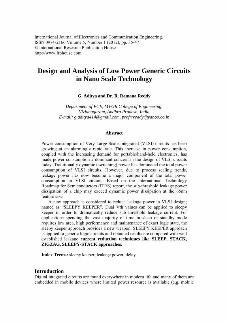
Figure 4c: 1bit adder circuit
Worst case delay, static power consumption, dynamic power consumption and area for all the approaches are measured as follows. Delay: Worst case propagation delay is measured for each approach. Input vectors and input/output triggers are chosen to measure the delay of a critical path. The propagation delay is measured from the trigger input edge reaching 50% of the supply voltage to the circuit output edge reaching 50% of the supply voltage value. Static Power: Static power is measured by asserting sets of input vectors in HSPICE. The average power dissipation over the specific subset of input combinations chosen is determined as the static power. Dynamic Power: For dynamic power measurement, clocked semi-random input vectors for a number of clock cycles are asserted, and average power dissipation during this time reported by HSPICE is considered as dynamic power consumption. Area: Layouts for all the considered approaches are designed 0.18μm process by using Microwind software. Areas for below 0.18μm technology are estimated by scaling the area of each approach layout designed based on 0.18μm process. Experimental Results Impact of Vth and transistor width for Chain Of Inverters

Design and Analysis of Lo
Impact of Vth Choosing the right Vth valof delay and power consutechnology, dynamic powbeen compared, i.e., base Vth. Vth of transistors is vstacked transistors in the parallel to the sleep transand 6 shows the measuredFrom Figure 5(a), it couldVth increases. The base csleepy keeper technique as While varying Vth at 2the same delay as the fokeeper with Vth = 0.37V 0.22V. At 270C, the sleepcase with Vth=0.36V, anddelay as the base case with2.5 times leakage reductio From Figure 6(b), it wunacceptable active powebecause large leakage popower consumption. Thisreduction techniques in na
Figure 5: Results for ChaPower c) Dynamic Power
ow Power Generic Circuits
lue of the sleepy keeper technique is very impumption. Therefore, using a chain of 4 inver
wer, static power and delay of the state-savingcase, stack, sleepy stack and sleepy keeper
varied as follows: all the transistors in the baforced stack case; and the sleep transistors istors in the sleepy stack and sleepy keeperd results while varying Vth at 270C and 1100
d be seen that stack inverter increases delay case also shows relatively large variation cos Vth changes. 270C, the sleepy keeper with Vth = 0.36V hasorced stack with Vth = 0.22V. Also, at 110
has exactly the same delay as the forced stpy keeper with Vth=0.36V has the same ded, at 1100C, the sleepy keeper with Vth=0.37h Vth=0.37V while the sleepy keeper achieve
on, respectively. was observed that the base case with Vth = er consumption when the temperature is ower consumption of the base case severes result emphasizes the importance of the anoscale technology.
ain of 4 Inverters at 270C, Varying Vth a)
41
portant in terms rters with 65nm g techniques are r, while varying ase case; one of plus transistors
r case. Figure 5 0C respectively. dramatically as ompared to the
s almost exactly 00C, the sleepy ack with Vth =
elay as the base V has the same
es 2.3 times and
0.2V consumes 1100C. This is
ely hurts active leakage power
Delay b) Static
42
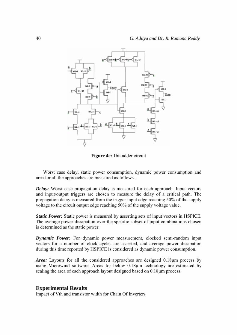
Figure 6: Results for ChaPower c) Dynamic Power Impact of Transistor WiThe Vth of the base case, 0.44V and for the stack thigh-Vth increases delay dshow that inverter chain dinitially the delay of theHowever, as transistor reduction, and the sleepy ktransistor width, but thconsumption than the sleep
G. Aditya and Dr. R. R
ain of 4 Inverters at 1100C, Varying Vth a) .
dth the sleepy stack and sleepy keeper technique
technique Vth is set 0.22V. Since the stack dramatically and the temperature is set to 27
delay decreases as transistor width increases.e base case and the sleepy keeper inverterwidth increases, sleepy keeper shows nokeeper and the base case achieve similar delae forced stack shows 26 times larger py keeper technique.
× W
Ramana Reddy
Delay b) Static
e is set to Vth = technique with
7oC. The results In Figure 7(a), r are different. oticeable delay ay using 4 times leakage power
× W

Design and Analysis of Low Power Generic Circuits 43
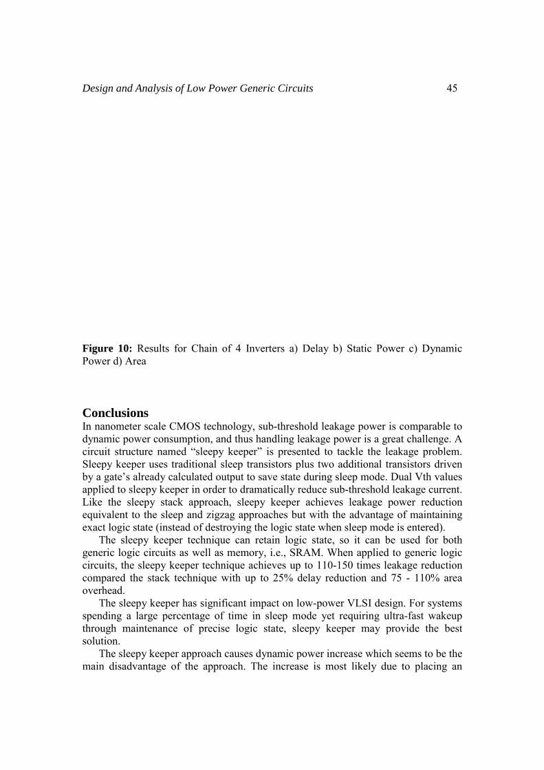
Figure 7: Results for Chain of Inverters, Varying Width at 270C a) Delay b) Static Power c) Dynamic Power Experimental Results for Generic Logic Circuits The Sleepy Keeper technique is compared with all the existing techniques in terms of delay, dynamic power, static power and area. In case of 45nm technologies the following results have been observed for Generic logic circuits like 4-bit adder, 4:1 Multiplexer, Chain of 4 Inverters. Figure 8 to 10 shows the graphs plotted in comparison with various technologies for delay, static power, dynamic power and area for the three test circuits. In 45nm technology, for a 4-bit adder test circuit the sleepy keeper approach (with dual Vth) achieves 114 times leakage reduction over the base case. The result is similar to the previous best leakage reduction technique with state saving, sleepy stack, but sleepy keeper achieves less delay than sleepy stack i.e. 43% less delay than sleepy stack with single Vth and 46% less delay with dual Vth. But Sleepy keeper consumes more dynamic power than sleepy stack. The area usage of the sleepy keeper is 76% smaller than area usage of the sleepy stack. In case of 4:1 Multiplexer test circuit the Sleepy keeper approach (with dual Vth) achieves 140 times leakage reduction over the base case and when compared to sleepy stack the result is almost similar but however sleepy keeper achieves 42% less delay than sleepy stack with single Vth and 45% less delay with dual Vth. The area usage for sleepy keeper is 35% smaller than the area usage of the sleepy stack. For a Chain of 4 inverters test circuit the keeper approach with dual Vth achieves 115 times leakage reduction over the base case and when compared to the stack approach it achieves 17 times leakage reduction. The sleepy keeper achieves less delay than the stack approach i.e. 53% less delay than the stack with single Vth and 35% less delay with dual Vth. The area usage of sleepy keeper is smaller than area usage of sleepy stack.
× W

44
Figure 8: Results for 4 bi
Figure 9: Results for 4:1 Area
G. Aditya and Dr. R. R
it adder a) Delay b) Static Power c) Dynamic
Multiplexer a) Delay b) Static Power c) Dyn
Ramana Reddy
Power d) Area
namic Power d)
Design and Analysis of Lo
Figure 10: Results for CPower d) Area Conclusions In nanometer scale CMOSdynamic power consumpticircuit structure named “sSleepy keeper uses traditiby a gate’s already calculaapplied to sleepy keeper inLike the sleepy stack apequivalent to the sleep anexact logic state (instead o The sleepy keeper tecgeneric logic circuits as wcircuits, the sleepy keepercompared the stack technoverhead. The sleepy keeper hasspending a large percentathrough maintenance of solution. The sleepy keeper appmain disadvantage of the
ow Power Generic Circuits
Chain of 4 Inverters a) Delay b) Static Pow
S technology, sub-threshold leakage power ision, and thus handling leakage power is a gresleepy keeper” is presented to tackle the leaional sleep transistors plus two additional traated output to save state during sleep mode. Dn order to dramatically reduce sub-threshold lpproach, sleepy keeper achieves leakage pnd zigzag approaches but with the advantageof destroying the logic state when sleep modechnique can retain logic state, so it can be
well as memory, i.e., SRAM. When applied tr technique achieves up to 110-150 times leanique with up to 25% delay reduction and 7
significant impact on low-power VLSI desigage of time in sleep mode yet requiring ultprecise logic state, sleepy keeper may pr
roach causes dynamic power increase which e approach. The increase is most likely due
45
wer c) Dynamic
s comparable to eat challenge. A akage problem. ansistors driven Dual Vth values leakage current. ower reduction of maintaining
e is entered). e used for both to generic logic akage reduction 75 - 110% area
gn. For systems tra-fast wakeup rovide the best
seems to be the e to placing an
46 G. Aditya and Dr. R. Ramana Reddy
NMOS transistor in a pull-up network and a PMOS transistor in a pull-down network where the two added transistors are controlled by the output voltage. References
[1] N. Kim, T. Austin, D. Baauw, T. Mudge, K. Flautner, and V. Narayanan, “Leakage current: Moore’s Lawmeets static power,” IEEE Comput., vol. 36, no. 12, pp. 68–75, Dec.2003.
[2] S. Mutoh et al., “1-V Power Supply High-speed Digital Circuit Technology with Multi threshold-Voltage CMOS,” IEEE Journal of Solid-State Circuits, Vol. 30, No. 8, pp. 847-854, August 1995.
[3] M. Powell, S.-H. Yang, B. Falsafi, K. Roy and T. N. Vijaykumar, “Gated-Vdd: A Circuit Technique to Reduce Leakage in Deep submicron Cache Memories,” International Symposium on Low Power Electronics and Design, pp. 90-95, July 2000.
[4] K.-S. Min, H. Kawaguchi and T. Sakurai, “Zigzag Super Cut-off CMOS Block Activation with Self-Adaptive Voltage Level Controller: An Alternative to Clock-gating Scheme in Leakage Dominant Era,” IEEE International Solid-State Circuits Conference, pp. 400-401, February 2003.
[5] Z. Chen, M. Johnson, L. Wei and K. Roy, “Estimation of Standby Leakage Power in CMOS Circuits Considering Accurate Modeling of Transistor Stacks,” International Symposium on Low Power Electronics and Design, pp. 239-244, August 1998.
[6] J.C. Park, V. J. Mooney III and P. Pfeiffenberger, “Sleepy Stack Reduction of Leakage Power,” Proceeding of the International Workshop on Power and Timing Modeling, Optimization and Simulation, pp. 148-158, September 2004.
[7] Se Hun Kim, Vincent J. Mooney III Sleepy Keeper: a New Approach to Low-leakage Power VLSI Design, VLSI, 2006 IFIP international conference.
[8] Tanner EDA, http://www.tannereda.com/. [9] Microwind EDA, http://www.microwind.net/.
[10] Synopsys Inc., http://www.synopsys.com/. [11] S. Kim and V. Mooney, “The Sleepy Keeper Approach: Methodology, Layout
and Power Results for a 4 bit Adder,” Technical Report GITCERCS-06-03, March 2006.
Design and Analysis of Lo
About Authors
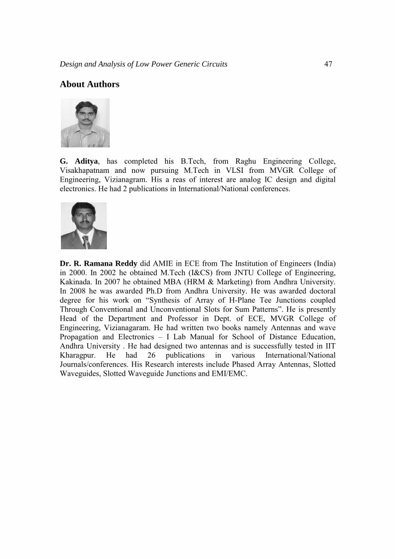
G. Aditya, has complVisakhapatnam and nowEngineering, Vizianagramelectronics. He had 2 publ
Dr. R. Ramana Reddy din 2000. In 2002 he obtaKakinada. In 2007 he obtIn 2008 he was awarded degree for his work on Through Conventional anHead of the DepartmenEngineering, VizianagaramPropagation and ElectronAndhra University . He hKharagpur. He had Journals/conferences. His Waveguides, Slotted Wav
ow Power Generic Circuits
leted his B.Tech, from Raghu Enginew pursuing M.Tech in VLSI from MVGm. His a reas of interest are analog IC deslications in International/National conferences
did AMIE in ECE from The Institution of Enained M.Tech (I&CS) from JNTU College otained MBA (HRM & Marketing) from And
Ph.D from Andhra University. He was aw“Synthesis of Array of H-Plane Tee Jun
nd Unconventional Slots for Sum Patterns”. nt and Professor in Dept. of ECE, MVGm. He had written two books namely Antenics – I Lab Manual for School of Distahad designed two antennas and is successful
26 publications in various InternaResearch interests include Phased Array An
eguide Junctions and EMI/EMC.
47
ering College, GR College of sign and digital s.
ngineers (India) of Engineering, dhra University. warded doctoral nctions coupled He is presently
GR College of ennas and wave ance Education, lly tested in IIT ational/National ntennas, Slotted