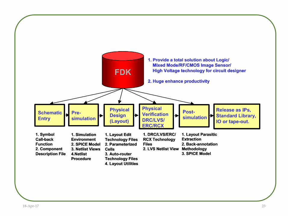
design and characterization of cmos inverter in cadence: a ...smdpc2sd.gov.in/downloads/iep/iep...
TRANSCRIPT

Design and Characterization of CMOSInverter in Cadence: A Tutorial
Mr. M. Tasleem Khan Mr. Harikrishna Veldandi
Workshop on Instruction Enhancement Programme (IEP)
18-Apr-17 1
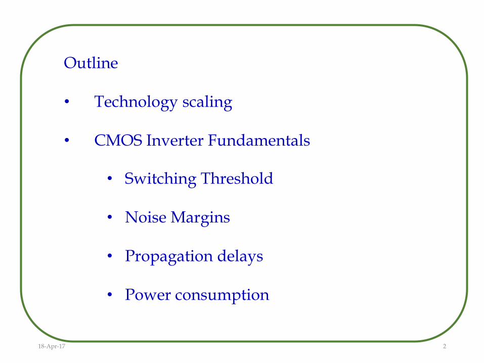
Outline
• Technology scaling
• CMOS Inverter Fundamentals
18-Apr-17 2
• Switching Threshold
• Noise Margins
• Propagation delays
• Power consumption
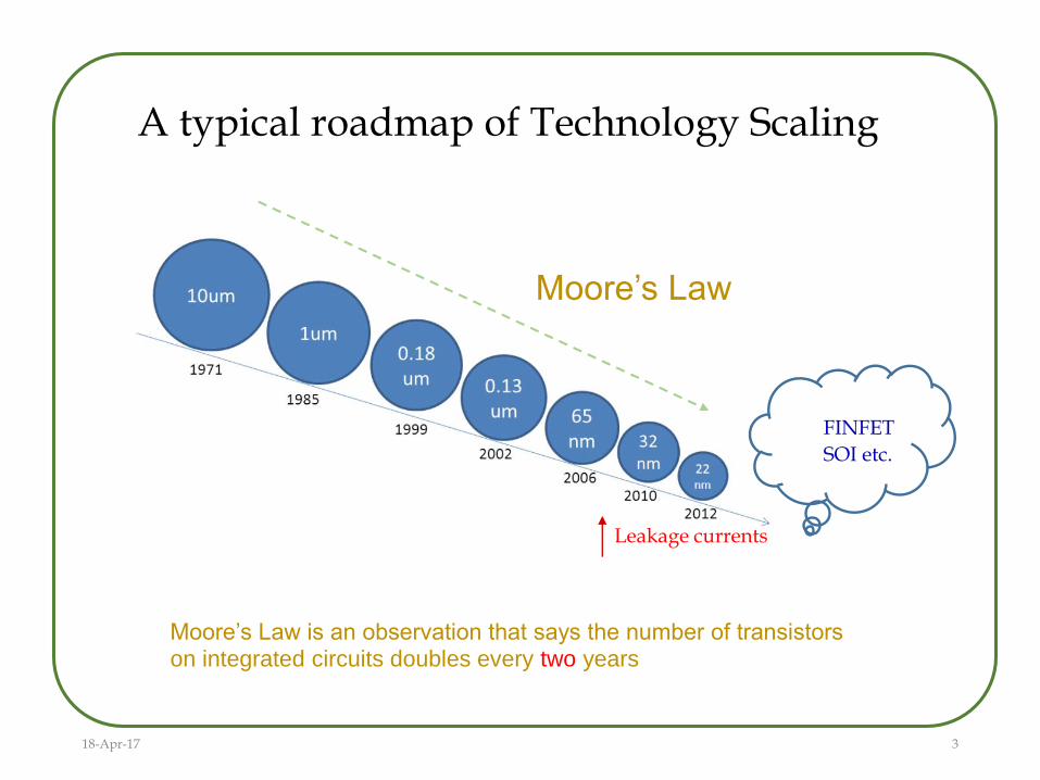
FINFET
SOI etc.
Moore’s Law is an observation that says the number of transistors on integrated circuits doubles every two years
A typical roadmap of Technology Scaling
Moore’s Law
18-Apr-17 3
Leakage currents
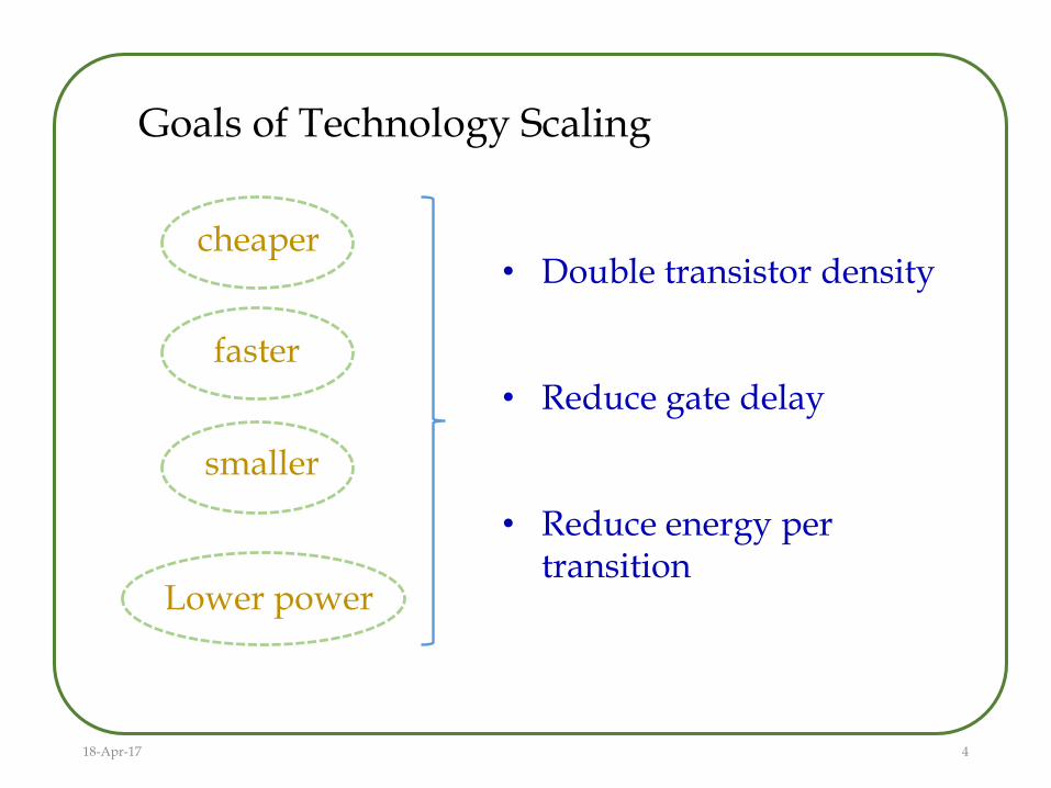
Goals of Technology Scaling
cheaper
faster
smaller
Lower power
• Double transistor density
• Reduce gate delay
• Reduce energy per transition
18-Apr-17 4

• Its all about designing the logic gates at transistor level so
that, it can be utilized in designs at algorithmic and
architectural levels.
• NAND and NOR are universal gates since they are readily
available in integrated-circuit form.
• The design analysis for NAND and NOR gates need
fundamentals of CMOS inverter.
• The objective of this presentation is to give gate level
design from transistor level perspective.
Digital IC Design
18-Apr-17 5
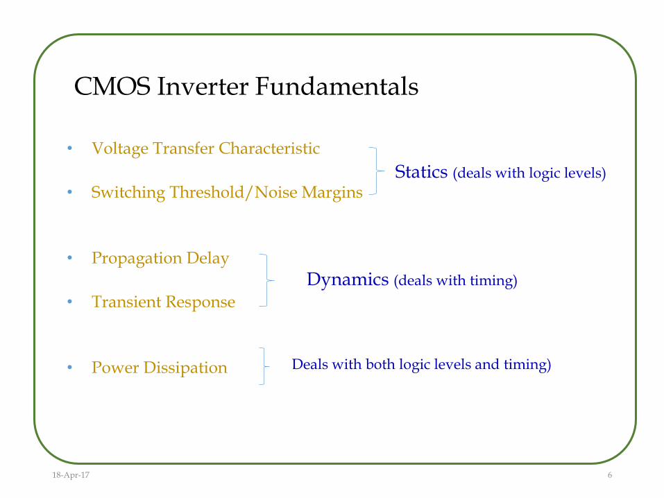
CMOS Inverter Fundamentals
• Voltage Transfer Characteristic
• Switching Threshold/Noise Margins
• Propagation Delay
• Transient Response
• Power Dissipation
Statics (deals with logic levels)
Dynamics (deals with timing)
18-Apr-17 6
Deals with both logic levels and timing)

Inverter Statics: Voltage Transfer CharacteristicsVDD
Vin Vout
CL
G S
D
D
G
S
Cutoff Linear Saturation
pMOS Vin -VDD= VGS> VT Vin -VDD=VGS< VT
Vin -Vout=VGD< VT
Vin -VDD=VGS> VT
Vin -Vout=VGD>VT
nMOS Vin = VGS< VT Vin =VGS> VT
Vin -Vout =VGD> VT
Vin =VGS> VT
Vin -Vout =VGD< VT
NMOS
PMOS
18-Apr-17 7

A typical VTC of inverter in 250 nm technology
00.5
1
1.52
2.5
0 0.5 1 1.5 2 2.5Vin (V)
Vo
ut(V
)
NMOS off
PMOS res
NMOS sat
PMOS res
NMOS sat
PMOS sat
NMOS res
PMOS sat NMOS res
PMOS off
• Curve characterizes CMOS inverter
1) What are the parameters that changes the shape
of this curve?
2) How does it affect the performance of inverter?

Impact of Process Variation and Supply Voltage
00.5
1
1.52
2.5
0 0.5 1 1.5 2 2.5Vin (V)
Vout(V
)
Nominal
Good PMOS
Bad NMOS
Bad PMOS
Good NMOS
Process variations (mostly) cause
a shift in the switching threshold
0
0.5
1
1.5
2
2.5
0 0.5 1 1.5 2 2.5
Vin (V)
Vout(V
)
Device threshold voltages
are kept (virtually) constant
Good transistor has smaller oxide thickness, smaller length, higher width and smaller threshold voltage; vice-versa for bad-transistor

0.8
0.9
1
1.1
1.2
1.3
1.4
1.5
0 1 10(W/L)p/(W/L)n (in semilog)
VM is relatively insensitive to variations in device
ratio, though it changes, for example, if ratios are 3,
2.5 and 2 then VM’s of 1.22V, 1.18V, and 1.13V
.1 ~3.4
-18
-16
-14
-12
-10
-8
-6
-4
-2
0
0 0.5 1 1.5 2Vin
(1+r)gain ----------------------------------
(VM-VTn-VDSATn/2)(n - p )
>>>determined technology parameters, especially and influence through VDD and VM
Variation of Switch Threshold and Gain

Noise Margins Determining VIH and VIL
0
1
2
3
VIL VIHVin
VOH = VDD
VM
By definition, VIH and VIL are
where dVout/dVin = -1 (= gain)
VOL =
GND
A piece-wise linear approximation of VTC
NMH = VDD - VIH
NML = VIL - GND
Approximating:
VIH = VM - VM /g
VIL = VM + (VDD - VM )/g
So high gain in the transition region is very
desirable

Dynamics of CMOS Inverter: Propagation delay
Propagation Delay, Tp: tpHL and tpLH always measured with respect to output and it
indicates how quickly output is affected by input.
•Measured between 50% transition from input to output
•Overall delay, tp, defined as the average of tpLH and tpHL i.e., (tpLH + tpHL)/2
tpHL
tpLH
t
t
Vin
Vout
50%
50%
tr
10%
90%
tf
Rise and fall time, Tr and Tf
•Defines slope of the signal
•Defined between the 10% and 90%
of the signal (affected by the
capacitance loads)
18-Apr-17 12

Switch Model: CMOS inverter
VDD
Rn
Vout
CL
Vin = V DD
VDD
Rp
Vout
CL
Vin = 0
Response time is determined by the time to charge CL through Rp (discharge CL
through Rn)
18-Apr-17 13

VDD
Vout
Vin = VDD
Ron
CL
tpHL = f(Ron.CL)
= 0.69 RonCL
t
Vout
VDD
RonCL
1
0.5
ln(0.5)
0.36
)/( LonCRt
OHout eVV
CMOS Inverter Propagation Delay
18-Apr-17 14

Tips to design a fast gate
•tpHL = f(Ron*CL)
•Keep output capacitance, CL, small
•low fan-out
•keep interconnections short (floor-plan your layout!)
•Decrease on-resistance, Ron ,of transistor
•increase W/L ratio
•make good contacts (slight effect)
18-Apr-17 15

A typical transient response of CMOS inverter
0 0.5 1 1.5 2 2.5
x 10-10
-0.5
0
0.5
1
1.5
2
2.5
3
t (sec)
Vout(V
)
tp = 0.69 CL (Reqn+Reqp)/2
tp
HL
tpL
H
18-Apr-17 16
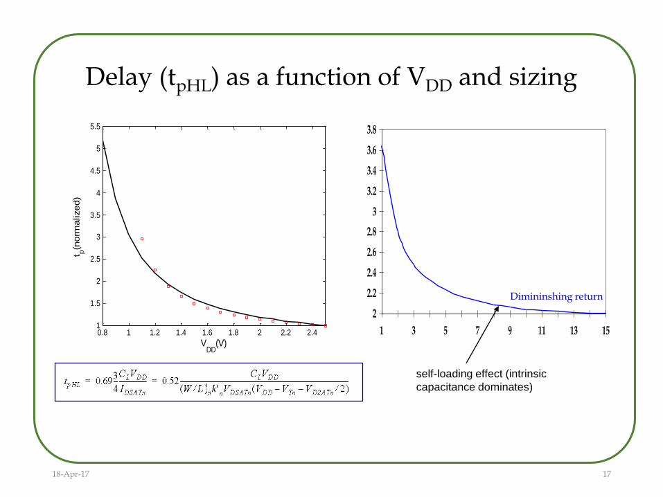
Delay (tpHL) as a function of VDD and sizing
0.8 1 1.2 1.4 1.6 1.8 2 2.2 2.41
1.5
2
2.5
3
3.5
4
4.5
5
5.5
VDD
(V)
t p(n
orm
alized)
2
2.2
2.4
2.6
2.8
3
3.2
3.4
3.6
3.8
1 3 5 7 9 11 13 15
self-loading effect (intrinsic
capacitance dominates)
Dimininshing return
18-Apr-17 17

PMOS/NMOS Ratio Effects
3
3.5
4
4.5
5
1 2 3 4 5
of 2.4 (= 31 k/13 k) gives
symmetrical response
of 1.9 gives optimal performance
= (W/Lp)/(W/Ln)
x 10-11
tpLH
tp
tpHL = aspect ratio of PMOS to aspect ratio of NMOS

Power Dissipation
• So far effect of input magnitude and timing of CMOS inverter
has been analyzed to design various paramters.
• How about combining both effects? It gives the birth of power
consumption in CMOS inverter.
• Power consumption determines heat dissipation and energy
consumption
Estimating power in CMOS requires different modeling!!!
18-Apr-17 19

Power Dissipation
•Power (in CMOS) = static power + dynamic power
•Dynamic power:
•(dis)charging capacitors
•temporary paths from VDD to VSS
•proportional to switching frequency
•Static power:
•static conductive paths between rails
•leakage
•increases with temperature
18-Apr-17 20
•Power consumption is related with propagation delay
•fast charge transfer => fast gate
•fast gate => more power consumption

Dynamic Power
Vin Vout
CL
Vdd
Energy/transition = C L * Vdd2
Power = Energy/transition * f = CL * Vdd2 * f
Need to reduce C L, Vdd , and f to reduce power.
Not a function of transistor sizes!
•No path exists between VDD and VSS in steady state
•No static power consumption! (ideally)
•Main reason why CMOS replaced NMOS
18-Apr-17 21

18-Apr-17 22
Thank You!!!
18-Apr-17 23

Switching Threshold
• VM where Vin = Vout (both PMOS and NMOS in saturation since VDS = VGS)
VM rVDD/(1 + r) where r = kpVDSATp/knVDSATn
• Switching threshold set by the ratio r, which compares the relative driving strengths of the PMOS and NMOS transistors
• Want VM = VDD/2 (to have comparable high and low noise margins), so want r 1
(W/L)p kn’VDSATn(VM-VTn-VDSATn/2)
(W/L)n kp’VDSATp(VDD-VM+VTp+VDSATp/2)=
18-Apr-17 24

Inverter Delay• Minimum length devices, L=0.25mm
• Assume that for WP = 2WN =2W
• same pull-up and pull-down currents
• approx. equal resistances RN = RP
• approx. equal rise tpLH and fall tpHL delays
• Analyze as an RC network
WNunit
Nunit
unit
PunitP RR
W
WR
W
WRR
11
tpHL = (ln 2) RNCL tpLH = (ln 2) RPCLDelay (D):
2W
W
unit
unit
gin CW
WC 3Load for the next stage:
18-Apr-17 25

Inverter with Load
Load (CL)
Delay
Assumptions: no load -> zero delay
CL
tp = k RWCL
RW
RW
Wunit = 1
k is a constant, equal to 0.69
18-Apr-17 26

Inverter with Load
Load
Delay
Cint CL
Delay = kRW(Cint + CL) = kRW Cint(1+ CL /Cint)
= Delay (Internal) + Delay (Load)
CN = Cunit
CP = 2Cunit
2W
W
18-Apr-17 27

Inverter Transient Response
-0.5
0
0.5
1
1.5
2
2.5
3
0 0.5 1 1.5 2 2.5
VDD=2.5V
0.25mm
W/Ln = 1.5
W/Lp = 4.5
Reqn= 13 k ( 1.5)
Reqp= 31 k ( 4.5)
tpHL = 36 psec
tpLH = 29 psec
so
tp = 32.5 psec
Vin
t (sec) x 10-10
tf trtpHL tpLH
From simulation: tpHL = 39.9 psec and tpLH = 31.7 psec

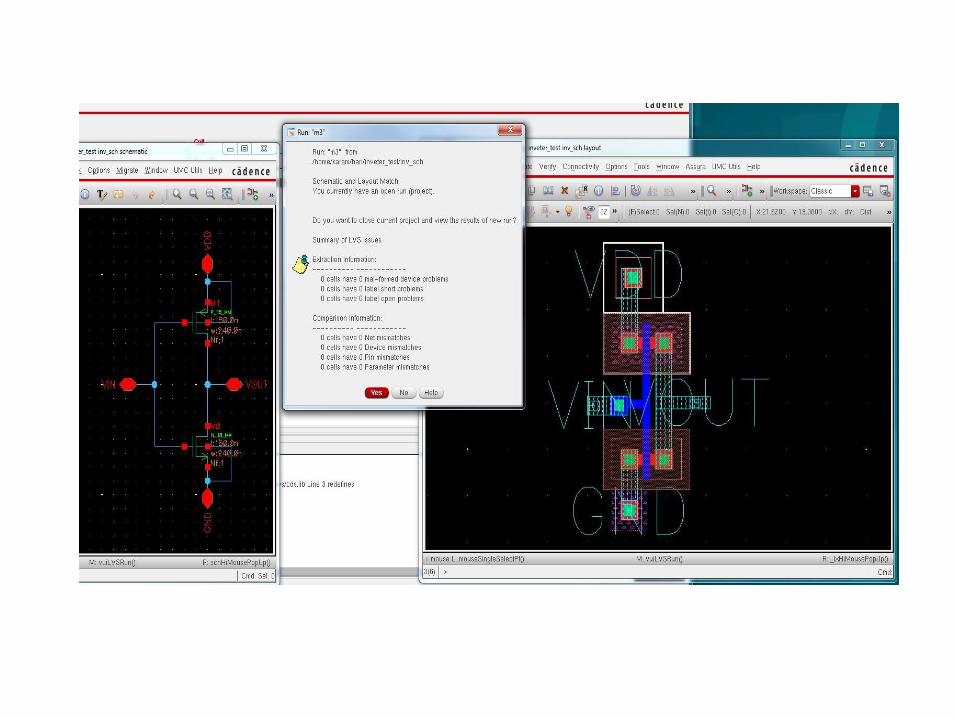
CMOS Inverter
CMOS NAND GateRing Oscillator

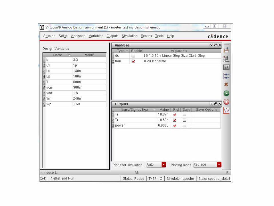
Design steps of CMOS Inverter
1. Plot the transient response of inverter with a minimum size of transistor
For 180 µm Technology Wn=Wp = 0.24 µm and Ln = Lp = 0.18 µm
2. Calculate the rise time (tr) and fall time (tf) of inverter and find the ratio (K)
3. Then size Wn = 0.24 µm, Wp = K Wn µm,
r
f
tK
t
Objective: Rise time and fall time of inverter should be the same and load CL= 5pF
1
2 p
fnT
Oscillation frequency of Ring Oscillator


35.53.27 3.3
10.83
r
f
t nK K
t n


Thank You!!!