design and characterization of standard cell library using
TRANSCRIPT

DESIGN AND CHARACTERIZATION OF STANDARD CELL LIBRARY USING
FINFETS
A Thesis
presented to
the Faculty of California Polytechnic State University,
San Luis Obispo
In Partial Fulfillment
of the Requirements for the Degree
Master of Science in Electrical Engineering
by
Phanindra Datta Sadhu
June 2021

© 2021
Phanindra Datta Sadhu
ALL RIGHTS RESERVED
ii

COMMITTEE MEMBERSHIP
TITLE: Design and Characterization of Standard
Cell Library Using FinFETs
AUTHOR: Phanindra Datta Sadhu
DATE SUBMITTED: June 2021
COMMITTEE CHAIR: Tina Smilkstein, Ph.D.
Associate Professor of Electrical and Computer Engineering
COMMITTEE MEMBER: Andrew Danowitz, Ph.D.
Associate Professor of Electrical and Computer Engineering
COMMITTEE MEMBER: Dennis Derickson, Ph.D.
Professor of Electrical Engineering
iii

ABSTRACT
Design and Characterization of Standard Cell Library Using FinFETs
Phanindra Datta Sadhu
The processors and digital circuits designed today contain billions of transistors on
a small piece of silicon. As devices are becoming smaller, slimmer, faster, and more
efficient, the transistors also have to keep up with the demands and needs of the daily
user. Unfortunately, the CMOS technology has reached its limit and cannot be used
to scale down due to the transistor’s breakdown caused by short channel effects. An
alternative solution to this is the FinFET transistor technology, where the gate of the
transistor is a three dimensional fin that surrounds the transistor and prevents the
breakdown caused by scaling and short channel effects. FinFET devices are reported
to have excellent control over short channel effects, high On/Off Ratio, extremely
low gate leakage current and relative immunization over gate edge line roughness.
Sub 20 nm node size is perceived to be the limit of scaling the CMOS transistors,
but FinFETs can be scaled down further because of its unique design. Due to these
advantages, the VLSI industry has now shifted to FinFET in implementation of their
designs. However, these transistors have not been completely opened to academia.
Analyzing and observing the effects of these devices can be pivotal in gaining an
in-depth understanding of them.
This thesis explores the implementation of FinFETs using a standard cell library
designed using these transistors. The FinFET package file used to design these cells
is a 15nm FinFET technology file developed by NCSU in collaboration with Cadence
and Mentor Graphics. Post design, the cells were characterized, the results were
analyzed and compared with cells designed using CMOS transistors at different node
sizes to understand and extrapolate conclusions on FinFET devices.
iv

ACKNOWLEDGMENTS
I would like to express my sincere gratitude to
• My advisor, Dr Tina Smilkstein for leading me through the process of complet-
ing my thesis and for her continual assistance and guidance through out my
graduate program at Cal Poly.
• The Committee members for taking the time to help review my work and pro-
vide valueable feedback.
• Electrical Engineering Department at Cal Poly for providing me with the tools
and resources to help complete my thesis.
• My parents and my brother who have unconditionally supported and loved me
through every endeavor I have embarked on.
v

TABLE OF CONTENTS
Page
LIST OF TABLES . . . . . . . . . . . . . . . . . . . . . . . . . . . . . . . . . ix
LIST OF FIGURES . . . . . . . . . . . . . . . . . . . . . . . . . . . . . . . . x
CHAPTER
1 Introduction . . . . . . . . . . . . . . . . . . . . . . . . . . . . . . . . . . . 1
1.1 Standard Cell Design Process Flow . . . . . . . . . . . . . . . . . . . 2
1.2 Standard Cell Library . . . . . . . . . . . . . . . . . . . . . . . . . . 2
1.2.1 Transistor Level View / Schematic View . . . . . . . . . . . . 3
1.2.2 Physical View . . . . . . . . . . . . . . . . . . . . . . . . . . . 4
1.2.3 Symbol View . . . . . . . . . . . . . . . . . . . . . . . . . . . 5
1.2.4 Behavioral View . . . . . . . . . . . . . . . . . . . . . . . . . . 5
1.2.5 Timing and Power Analysis . . . . . . . . . . . . . . . . . . . 6
1.3 Tools Utilized . . . . . . . . . . . . . . . . . . . . . . . . . . . . . . . 6
1.4 Cell Design Process Flow . . . . . . . . . . . . . . . . . . . . . . . . . 6
2 Background . . . . . . . . . . . . . . . . . . . . . . . . . . . . . . . . . . . 8
2.1 Moore’s Law . . . . . . . . . . . . . . . . . . . . . . . . . . . . . . . . 8
2.2 MOSFET Scaling . . . . . . . . . . . . . . . . . . . . . . . . . . . . . 9
2.3 Short Channel Effects . . . . . . . . . . . . . . . . . . . . . . . . . . 10
2.3.1 Impact Ionization . . . . . . . . . . . . . . . . . . . . . . . . . 10
2.3.2 Drain Induced Barrier Lowering . . . . . . . . . . . . . . . . . 11
2.3.3 Surface Scattering . . . . . . . . . . . . . . . . . . . . . . . . . 12
2.3.4 Velocity Saturation . . . . . . . . . . . . . . . . . . . . . . . . 12
2.3.5 Hot Carrier Injection . . . . . . . . . . . . . . . . . . . . . . . 13
vi

2.4 FinFETs . . . . . . . . . . . . . . . . . . . . . . . . . . . . . . . . . . 14
2.4.1 Architecture of FinFET . . . . . . . . . . . . . . . . . . . . . 14
2.4.2 Device Operation . . . . . . . . . . . . . . . . . . . . . . . . . 15
2.4.3 Device Characteristics . . . . . . . . . . . . . . . . . . . . . . 16
2.4.3.1 Drain Current Equation . . . . . . . . . . . . . . . . 16
2.4.3.2 I-V Characteristics . . . . . . . . . . . . . . . . . . . 16
2.4.3.3 Sub-Threshold Slope . . . . . . . . . . . . . . . . . . 18
2.4.3.4 Power Dissipation . . . . . . . . . . . . . . . . . . . 19
2.4.3.5 Leakage Currents . . . . . . . . . . . . . . . . . . . 20
2.5 FinFET Design Challenges . . . . . . . . . . . . . . . . . . . . . . . . 21
2.5.1 Fin Patterning . . . . . . . . . . . . . . . . . . . . . . . . . . 21
2.5.2 Fin Shape . . . . . . . . . . . . . . . . . . . . . . . . . . . . . 22
2.5.3 FinFET Parasitic Capacitance . . . . . . . . . . . . . . . . . . 23
2.5.4 Fin Isolation . . . . . . . . . . . . . . . . . . . . . . . . . . . . 24
2.6 New Transistor Technologies . . . . . . . . . . . . . . . . . . . . . . . 25
3 Design . . . . . . . . . . . . . . . . . . . . . . . . . . . . . . . . . . . . . . 27
3.1 Components of Standard Cell Library . . . . . . . . . . . . . . . . . . 27
3.2 Layout Architecture . . . . . . . . . . . . . . . . . . . . . . . . . . . 28
3.2.1 Back End of Line (BEOL) Layers . . . . . . . . . . . . . . . . 29
3.2.2 Middle of Line (MOL) Layers . . . . . . . . . . . . . . . . . . 29
3.2.3 Front End of Line (FEOL) Layers . . . . . . . . . . . . . . . . 30
3.2.4 Standard Design Rules . . . . . . . . . . . . . . . . . . . . . . 30
3.2.5 Cell Measurements . . . . . . . . . . . . . . . . . . . . . . . . 31
3.3 Cell Design . . . . . . . . . . . . . . . . . . . . . . . . . . . . . . . . 33
3.3.1 List of cells designed . . . . . . . . . . . . . . . . . . . . . . . 33
vii

3.3.2 Logic Gates . . . . . . . . . . . . . . . . . . . . . . . . . . . . 34
3.3.2.1 2 Input Gates . . . . . . . . . . . . . . . . . . . . . . 34
3.3.2.2 3 Input Gates . . . . . . . . . . . . . . . . . . . . . . 36
3.3.3 Adders . . . . . . . . . . . . . . . . . . . . . . . . . . . . . . . 37
3.3.3.1 Half Adder . . . . . . . . . . . . . . . . . . . . . . . 37
3.3.3.2 Full Adder . . . . . . . . . . . . . . . . . . . . . . . 38
3.3.4 Flip Flop . . . . . . . . . . . . . . . . . . . . . . . . . . . . . 38
3.3.4.1 D- Flip Flop . . . . . . . . . . . . . . . . . . . . . . 38
3.3.5 Multiplexer . . . . . . . . . . . . . . . . . . . . . . . . . . . . 39
3.3.5.1 2x1 MUX . . . . . . . . . . . . . . . . . . . . . . . . 39
3.4 Library Characterization . . . . . . . . . . . . . . . . . . . . . . . . . 40
3.4.1 Liberty File . . . . . . . . . . . . . . . . . . . . . . . . . . . . 41
4 Results . . . . . . . . . . . . . . . . . . . . . . . . . . . . . . . . . . . . . . 44
4.1 Small Signal Analysis . . . . . . . . . . . . . . . . . . . . . . . . . . . 44
4.2 Power and Delay of Cells . . . . . . . . . . . . . . . . . . . . . . . . . 46
4.3 Ripple Carry Adder . . . . . . . . . . . . . . . . . . . . . . . . . . . . 47
4.4 D- Flip Flop . . . . . . . . . . . . . . . . . . . . . . . . . . . . . . . . 48
5 Future Work . . . . . . . . . . . . . . . . . . . . . . . . . . . . . . . . . . 50
6 Conclusion . . . . . . . . . . . . . . . . . . . . . . . . . . . . . . . . . . . . 52
BIBLIOGRAPHY . . . . . . . . . . . . . . . . . . . . . . . . . . . . . . . . . 53
APPENDICES
A Liberate Script . . . . . . . . . . . . . . . . . . . . . . . . . . . . . . 58
A.1 Library Cell Characterization . . . . . . . . . . . . . . . . . . . . . . 58
A.2 Power and Timing Arcs for NOR2, Inverter and DFF . . . . . . . . . 58
viii

LIST OF TABLES
Table Page
3.1 Cell measurements . . . . . . . . . . . . . . . . . . . . . . . . . . . 32
3.2 List of the cells designed in the standard cell library . . . . . . . . . 33
4.1 Tabulation of metrics for the cells designed in standard cell libraries 46
4.2 Comparison of performance metrics of CMOS and FinFET RippleCarry adder . . . . . . . . . . . . . . . . . . . . . . . . . . . . . . . 47
4.3 Simulation results of DFF cells compared to state of the art flip flops. 48
ix

LIST OF FIGURES
Figure Page
1.1 Process flow of design of standard cell library . . . . . . . . . . . . 2
1.2 Transistor level view of Inverter . . . . . . . . . . . . . . . . . . . . 3
1.3 Physical view of Inverter . . . . . . . . . . . . . . . . . . . . . . . . 4
1.4 Symbol view of Inverter . . . . . . . . . . . . . . . . . . . . . . . . 5
1.5 Verilog A code for NAND2 gate . . . . . . . . . . . . . . . . . . . 5
1.6 Custom design flow . . . . . . . . . . . . . . . . . . . . . . . . . . . 7
2.1 Moore’s Law : Transistor scaling over the years . . . . . . . . . . . 8
2.2 The ionized electron collides with the electron-hole pairs near thedrain . . . . . . . . . . . . . . . . . . . . . . . . . . . . . . . . . . 10
2.3 The impact of scaling on potential barrier between source and drain 11
2.4 Zig-zag path of the electron reducing its mobility . . . . . . . . . . 12
2.5 Electron trapped inside the oxide after the collusion . . . . . . . . . 13
2.6 The structure of a FinFET transistor . . . . . . . . . . . . . . . . . 15
2.7 (a) IV Curve of FinFET (left) (b) IV Curve of MOSFET (right)[1] 17
2.8 Comparision between the ON/Off ratio between MOSFET and CMOS[1] 17
2.9 logIds vs gate voltage Vgs to calculate the sub threshold swing ofFinFET device[2] . . . . . . . . . . . . . . . . . . . . . . . . . . . . 18
2.10 Top level view : SEM image of gates patterned over Fins[3] . . . . . 22
2.11 Fin shape in a FinFET showcasing the sloped side walls [4] . . . . . 23
3.1 Cross section of layout of FinFET [5] . . . . . . . . . . . . . . . . 28
3.2 Cell rail and pitch measurements for an Inverter cell . . . . . . . . 32
x

3.3 Screen captures of (a) Schematic (b) Symbol and (c) Layout of aNAND2 logic gate . . . . . . . . . . . . . . . . . . . . . . . . . . . 34
3.4 Screen captures of (a) Schematic (b) Symbol and (c) Layout of aOR2 logic gate . . . . . . . . . . . . . . . . . . . . . . . . . . . . . 35
3.5 Screen captures of (a) Schematic (b) Symbol and (c) Layout of aXOR2 logic gate . . . . . . . . . . . . . . . . . . . . . . . . . . . . 35
3.6 Screen captures of (a) Schematic (b) Symbol and (c) Layout of aNOR3 logic gate . . . . . . . . . . . . . . . . . . . . . . . . . . . . 36
3.7 Screen captures of (a) Schematic (b) Symbol and (c) Layout of aAND3 logic gate . . . . . . . . . . . . . . . . . . . . . . . . . . . . 36
3.8 Screen captures of (a) Schematic (b) Symbol and (c) Layout of aHalf Adder logic cell . . . . . . . . . . . . . . . . . . . . . . . . . . 37
3.9 Screen captures of (a) Schematic (b) Symbol and (c) Layout of a Fulladder logic cell . . . . . . . . . . . . . . . . . . . . . . . . . . . . . 38
3.10 Screen captures of (a) Schematic (b) Symbol and (c) Layout of aD-Flip Flop logic cell . . . . . . . . . . . . . . . . . . . . . . . . . . 39
3.11 Screen captures of (a) Schematic (b) Symbol and (c) Layout of a 2X1Multiplexer logic cell . . . . . . . . . . . . . . . . . . . . . . . . . . 40
3.12 Objectives of characterization [6] . . . . . . . . . . . . . . . . . . . 41
3.13 Process flow of a liberty file.[6] . . . . . . . . . . . . . . . . . . . . 42
4.1 Schematic of 4- bit ripple carry adder . . . . . . . . . . . . . . . . . 47
4.2 Comparison of performance metrics of TSMC 180nm and FreePDK15Ripple carry adder . . . . . . . . . . . . . . . . . . . . . . . . . . . 48
xi

Chapter 1
INTRODUCTION
Circuits in general are designed and tested at a high level of abstraction using hard-
ware description languages (HDL) such as VHDL or Verilog. Digital circuits which
don’t require a high level of performance are designed using HDL as it is economical,
require lower testing and require less time to market . High performance circuits are
still done by hand. The behavioral description of the design is synthesized into a logic
netlist using synthesis tools such as Cadence Virtuoso or Genus. These logic blocks
are then translated into netlists and then layout using these software tools and are
then optimized in design environment which contain descriptions of all logic primi-
tives. The logical netlist generated by these synthesis tools contain the definition of
digital circuits. These units or cells are called standard cells and their collection is
called as a standard cell library. The most basic standard cell definitions are NOR
and NAND gates which are also known as universal gates and also the commonly
used inverter gate using which all combinational circuits can be implemented. The
HDL synthesis tool utilizes this behavioral description and creates a logic that re-
alises behavior description of these cells. For the design of this standard cell library
NCSU PDK 15 was used which is a 15 nm FinFET library developed by NCSU
along with Cadence. This is a FinFET based predictive process design kit, which
enables circuit level and device level analysis of the 15 nm FinFET technology node.
1

1.1 Standard Cell Design Process Flow
Figure 1.1: Process flow of design of standard cell library
Development of standard cell library starts by designing the cells using digital circuits.
In order to develop the circuits design tools require design PDK (Process Development
Kit) and model files which contain the SPICE of the transistors. Next Step is the
circuit design where the user generates a schematic and the tool converts the design
into a netlist file (.cdl). Then, physical design of the circuit is done where the circuit is
drawn in silicon and routed using metal layers and the design tool generates a layout
file (GDSII). Final step is characterization where the user feeds in a script and tools
generate a datasheet with all its values and a verilog files so that the library can be
used by HDL and be synthesized using Cadence Genus tool for design of Circuits and
Systems based on FinFETs. In further chapters of this thesis, a detailed outline of the
FinFET transistors and their operation are discussed. The design and the decisions
taken while designing the cells, and characterization of the cells are elaborated.
1.2 Standard Cell Library
A Standard cell library[7] is a collection of well defined and characterized logic gates
that can be used by a synthesis tool to implement a digital design or design a system.
2

These standard cells are the building blocks of digital systems. Standard cells must
meet the definition and the specification of the system which are manipulated by
synthesis, place and route algorithms and characterization tools. To define a standard
cell EDA (Electronic Design Automation) are provide a collection technology files with
all the information needed. While designing a standard cell library great attention is
paid to various parameters such as cell dimensions, voltage rails, pin placement, metal
layers and PR boundary. Generally standard cells contain the fundamental cells which
are required for design and development of any digital circuit include combinational
logic cells such as NAND, NOR and inverter, sequential logic cells such as flip flops
or latches and other cells such as filler cells, tap cells. To develop cells in standard
cell library the cell architecture is developed using various view which are as follow
1.2.1 Transistor Level View / Schematic View
This view of a transistor cell generates a netlist at the transistor level of the cell. A
netlist is a textual description of a circuit and its components. Netlist is a connection
of gates and can also include resistors, capacitors and transistors used in analog sim-
ulation. A schematic tool such as cadence virtuoso generates a netlist file. Schematic
views are used to simulate and test the functional behaviour of the cell. The Figure
1.2 gives an example of a transistor level view of inverter.
Figure 1.2: Transistor level view of Inverter
3

1.2.2 Physical View
This view includes the layout which is the physical implementation of the the transis-
tor view where the design is drawn in silicon with metal layers used for routing and
adding components like resistors, capacitors and probe pads etc. Th layout of the
cells follows the architecture of the cell and the design rules which are determined by
the founderies. The layout is also used to extract the parasitic capacitances and the
resistances of the cell design. Figure 1.3 shows the layout of an inverter cell.
Figure 1.3: Physical view of Inverter
4

1.2.3 Symbol View
This view defines symbols for the cells which can be later utilized to develop schemat-
ics of a larger design. Figure 1.4 shows the symbol view of an inverter.
Figure 1.4: Symbol view of Inverter
1.2.4 Behavioral View
This comprises of the verilog description of the cells which is used for simulation and
logical equivalence. This view makes it easy for the user to understand the operation
of the cell and develop a more precise functionality. Cadence tools accepts Verilog A
to define the functional and behavioral description of the cell.
Figure 1.5: Verilog A code for NAND2 gate
5

1.2.5 Timing and Power Analysis
This step is also known as characterization which performs STA (Static Timing Anal-
ysis) and power analysis for the cells. Liberty files are generated for operating condi-
tions of the library. These files give a the performance metrics of the cell.
1.3 Tools Utilized
• Cadence Virtuoso : Transistor Level Schematic and Entry tool for Design
• Cadence Spectre ADE : Simulation of the design
• Cadence Layout XL : Layout of the Design
• Cadence Virtuoso : Export GDS
• Cadence Liberate : Characterization of the Cells
1.4 Cell Design Process Flow
Full custom design [8] is often considered when designing a high performance circuit.
The routing of the critical wires is considered to be the important gap between the
design flows. Often this design flow is more time consuming to design as it requires
most of the views to be hand drawn. Semi custom[9] design flow utilizes standard
cells to design circuits where the tools like Cadence Genus uses these cells synthesize
circuits and generates RTL (Register Transfer Level) design with all the timing and
capacitance data . Place and rout is which is considered the key difference between
Semi-custom and custom process flow[10] done manually by the user rather than
the machine where it performs automatic place and route of the circuits in the later
6

process. Once the standard cell is designed and characterized users can use the semi-
custom design flow to design their circuits using cadence Genus.
Figure 1.6: Custom design flow
7

Chapter 2
BACKGROUND
2.1 Moore’s Law
In 1965 Gordon Moore published a famous paper describing the evolution of transis-
tors’ density in integrated circuits. He predicted that the number of transistors in a
dense integrated circuit doubles every two years[11]. This prediction later came to
be known as Moore’s Law. This law has been the cornerstone of the industry and
has been used to planning and set targets for the research and development of new
semiconductor-based technologies. Since 1990 semiconductor companies have collab-
orated to predict this trend with higher precision. This initiative garnered and led to
the International Technology Roadmap for Semiconductors (ITRS); ever since then,
ITRS issues an annual report that services as a benchmark for the industries and
recognizes the latest trends and developments in the industry.
Figure 2.1: Moore’s Law : Transistor scaling over the years
8

This observation has been valid until now, but due to the limitations in technology,
this prediction has come to a predicted to come to an end. The end of this prophecy
has pushed academia and research to look beyond the current technologies to develop
new ideas to overcome their limitations. One such idea was to extend the gate of
the transistors, which controls the flow of electrons and electric field, and develop
a 3D structure that would result in better control and enable scaling down of these
transistors. This led to the design and development of 3D transistors, which would
begin a new era of devices that would continue the trend predicted by Moore.
2.2 MOSFET Scaling
The semiconductor industry’s workhorse technology is the CMOS, and MOSFET is
the fundamental building block of the CMOS technology. In order to keep up with
the growth and pace of Moore’s law, the linear dimensions of the transistor were to
be reduced by half almost every three years. By the early 2010s, transistors at 20
nm gate length had become commonly used by IC (Integrated Circuit) designers.
The development of SOI (Silicon on Insulators), in which transistors are made on a
thin layer of silicon on top of a silicon dioxide layer, led to the surge in speed and
power consumption due to reduction in capacitance. As the dimensions started to
reduce even further, the proximity between the source and drain pins reduced the
ability of the gate to control the potential and leakage current in the channel region
and additionally caused undesirable effects called short channel effects. Due to these
issues, it became impossible to shrink the MOSFET below 20nm node size.
9
2.3 Short Channel Effects
The main drives for reducing the size of the transistors, i.e., their lengths, are in-
creasing speed and reducing cost. When you make circuits smaller, their capacitance
reduces, thereby increasing operating speed. Similarly, smaller circuits allow more of
them in the same wafer, dividing the total cost of a single wafer among more dies to
increase yield.
However, with a great reduction in size come great problems, in this case in the form
of unwanted side effects, the so-called short-channel effects[12]. When the MOSFET
channel becomes the same order of magnitude as the depletion layer width of source
and drain, the transistors start behaving differently, which impacts performance, mod-
eling, and reliability. These effects can be divided among the following:
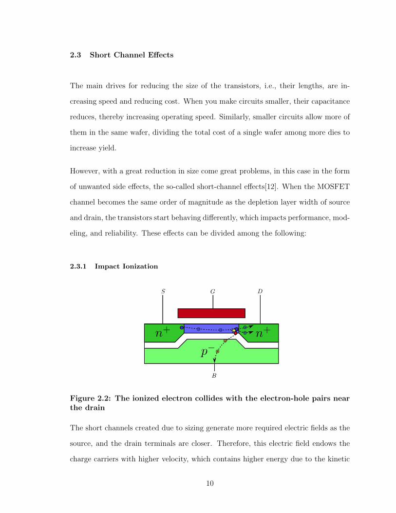
2.3.1 Impact Ionization
Figure 2.2: The ionized electron collides with the electron-hole pairs nearthe drain
The short channels created due to sizing generate more required electric fields as the
source, and the drain terminals are closer. Therefore, this electric field endows the
charge carriers with higher velocity, which contains higher energy due to the kinetic
10

energy stored in the carriers. The electric field is proportional to drain-source voltage
and inversely proportional to the distance between source and drain. The electrons
with higher energy tend to strike an electron off the conduction band. The generated
electron-hole pair from the conduction band gets displaced, the hole from the pair
gets attracted to the bulk, and the electron tries to move back to the drain. This
results in the formation of a bipolar parasitic junction between source and drain.
Another problem that arises due to this is that the electron displaced can cause an
avalanche effect by displacing more electrons from the lattice, thereby leading to a
current that the gate voltage cannot control.
2.3.2 Drain Induced Barrier Lowering
Figure 2.3: The impact of scaling on potential barrier between source anddrain
Under normal conditions in a CMOS, a potential barrier prevents electrons from
flowing between source and drain. The gate voltage has the function of lowering this
voltage to the point where electrons freely start flowing from the gate to the source.
Due to scaling, when the size of the channel becomes shorter, a larger drain voltage
11

would widen the depletion region to the point where it reduces the size of the potential
barrier, which results in the reduction of channel mobility.
2.3.3 Surface Scattering
Figure 2.4: Zig-zag path of the electron reducing its mobility
In the channel of a CMOS transistor, the charge carriers move with a very high ve-
locity under the influence of the field generated by the gate, due to which they keep
crashing and bouncing off the surface—the carriers in the channel move in a zig-zag
path during their travel. As the length of the channel becomes shorter, the lateral
electric field created by the gate and voltage V ds becomes stronger. To compensate
for that, the vertical electric field created by the gate voltage needs to increase pro-
portionally, which can be achieved by reducing the oxide thickness. As a side effect,
surface scattering becomes heavier, reducing the adequate mobility compared to more
extended channel technology nodes.
2.3.4 Velocity Saturation
The velocity of the charged carriers is directly dependent on the electric field generated
by the gate voltage. As this field gets stronger due to sizing, the velocity tends to
saturate, which results in reduced mobility. This effect is common to the MOSFET
12
transistors as they tend to have higher electric fields. Velocity saturation is only
apparent when the current saturates due to velocity saturation before saturating due
to pinch-off. That means that the drain-source saturation voltage will be lower than
VGS − VTH in short channel transistors. An example is illustrated below 2.1 to show
velocity saturation.
Esaturaton = 104 V
cm
SiliconSat V el = 107 cm
s
V DS5µm = 5µm ∗ 104 V
cm
= 5 ∗ 10−6 ∗ 104
10−3V = 500V
V DS5nm = 5nm ∗ 104 V
cm
= 5 ∗ 10−9 ∗ 104
10−3V = 0.5V
(2.1)
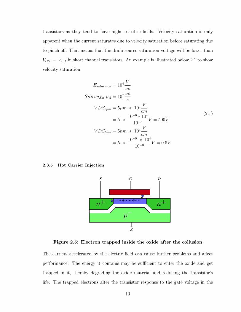
2.3.5 Hot Carrier Injection
Figure 2.5: Electron trapped inside the oxide after the collusion
The carriers accelerated by the electric field can cause further problems and affect
performance. The energy it contains may be sufficient to enter the oxide and get
trapped in it, thereby degrading the oxide material and reducing the transistor’s
life. The trapped electrons alter the transistor response to the gate voltage in the
13

form of an increased threshold voltage. This effect is unrecoverable and destroys the
transistor.
2.4 FinFETs
A FinFET or a fin Field Effect Transistor is a metal-oxide-semiconductor device where
the gate is placed between either side of the semiconductor body. Chenming Hu de-
veloped this device at the University of California Microfabrication lab, Berkeley[13].
The Fin in the acronym describes a thin body fin of semiconductor material. In a
finfet structure, the gate may be placed on two or more sides or all around it in
order to improve its device performance. FinFETs offer significantly higher speed
and current drive over MOSFET’s due to reduced capacitance despite not having
any drain-source bulk capacitance. Recognizing its advantages, Intel was the first
company in the industry to introduce FinFET technology at a 22 nm node in mass
production in the year 2011.
2.4.1 Architecture of FinFET
The FinFET transistor is the solution for all the above-mentioned short channel
effects. Officially it was called the tri-gate transistor as it covered the channel on
all three sides. The principle behind the structures[14] is a thin body, so the gate
capacitance is closer to the whole channel. The body is very thin so that no leakage
path is far from the gate. Therefore the gate can have more control of the voltage.
FinFETs can be implemented either on bulk silicon or SOI wafer. This FinFET
structure consists of a thin fin of silicon body on a substrate. The gate is wrapped
around the channel providing excellent control from three sides of the channel. This
structure is called the FinFET because its Si body resembles the back Fin of a fish.
14

Figure 2.6: The structure of a FinFET transistor
For a FinFET, the height of the channel determines the width of the device. The
following equation gives the perfect width of the channel.
Width of the Channel = 2 (Fin Height) + Fin Thickness (2.2)
The drive current of the FinFET can be increased by increasing the width of the
channel, therefore, by increasing the height of the Fin.
2.4.2 Device Operation
A FinFET device has three modes of operation: linear, saturation, and cutoff, similar
to that of the MOSFET. The theories developed for MOSFET transistors can be
extrapolated for defining the device operation[2] of FinFETs. In a common gate set
up of a FinFET transistor device operation with bias Vs = 0 and a drain voltage Vds
with reference to the source is applied to the drain, so that source-drain junction is
reverse biased. Under this biasing condition, the body current and the gate current
15

are zero. The applied gate voltage with reference to source bias Vgs controls the
surface carrier densities. A certain value of Vgs, defined as the threshold voltage
(Vth), is required to create the channel inversion layer, where Vth is determined by
the properties of the structure. For Vgs > Vth, an inversion layer exists, that is, a
conducting channel exists from the drain to the source of the device, and a drain
current IDS will flow.
2.4.3 Device Characteristics
2.4.3.1 Drain Current Equation
The drain current equation of FinFET transistors is similar to that of the MOSFET
devices. The drain current equation[2] in linear region is given by
IDS = 2 µ CoxW
L(Vgs − Vth −
VDS2
) VDS
where W = 2 ∗ (Height of F in) + Thickness of F in
(2.3)
2.4.3.2 I-V Characteristics
The IV characteristics, i.e., the Id vs. Vds plot for FinFET, are similar to that of the
CMOS plot, but there are slight variations between the two plots. The two features
that can be derived from the plots are level of ON current and the output resistance in
the strong inversion region.The higher ON current and output resistance in FinFet is
due to the channel being surrounded in three dimensions which results in better gate
control. Fig. 2.8 shows ION/IOFF ratio versus supply voltage for both devices. As
illustrated, in low supply voltages, the ION/IOFF ratio is higher for FinFET, while in
16

Figure 2.7: (a) IV Curve of FinFET (left) (b) IV Curve of MOSFET(right)[1]
Figure 2.8: Comparision between the ON/Off ratio between MOSFET andCMOS[1]
high supply voltages, it is higher for bulk MOSFET. It is because bulk MOSFET has a
lower IOFF compared with FinFET, while FinFET has a higher ION. In low supply
voltages, the OFF current of bulk MOSFET is lower, but it is closed to FinFET,
while the ON current of FinFET is much higher than bulk MOSFET. As a result,
the ION/IOFF ratio is higher for FinFET. However, in high supply voltages, the
ON current of bulk MOSFET is getting close to the ON current of FinFET, and the
ION/IOFF ratio of devices is closed to each other[1].
17

2.4.3.3 Sub-Threshold Slope
A vital characteristic of the subthreshold operation is the gate voltage swing of the
device. This gate voltage is also known as sub-threshold swing [2]. It is the quantified
as the inverse of the slope of the the Ids − V gs plot and defined as the change in
gate voltage Vgs required to change the drain current IDS by one decade. Therefore
Figure 2.9: logIds vs gate voltage Vgs to calculate the sub threshold swingof FinFET device[2]
the sub-threshold swing measures the On-off characteristics of the FinFET device. In
figure 2.9 if we take the points shown and then by definition (Vgs2− Vgs1) required to
change the ratio of (Ids2/Ids1) by one decade or a 10[2] is defined as
Subthreshold Swing =Vgs2 − Vgs1
logIds2 − logIds1=
dVgsd(logIds)
= 2.3dVgs
d(lnIds)(2.4)
In the above equation 2.3(logIds) was used to convert log to natural logarithm (ln).
So based on this, it is directly dependent on the drain current IDS; however, this
variation is negligible over one decade of current.
18

2.4.3.4 Power Dissipation
Power dissipation [15] in any circuit primarily comes from two components dynamic
and static.
Ptotal = PDynamic + PLeakage (2.5)
• Dynamic Power: Dynamic power [15]VDD, and the designer decides the oper-
ating frequency. To evaluate the power, the capacitance at every node of the
circuit is measured. The operation of digital circuits requires continuous switch-
ing between the transistors, thus causes a charge build-up at nodes and results
in capacitance. Capacitance directly affects the power consumption of a digital
circuit. The capacitance is measured by evaluating the sum of the gate, diffu-
sion, and the wire capacitance of the node multiplied by the activity factor (α).
The switching power, which is the major contributing factor in dynamic power,
is calculated by taking the worst-case measuring the effective capacitances of
all the nodes. Therefore to design a circuit with low power consumption, the
terms of switching power have to be reduced. Since VDD varies quadratically
with the power consumption, it is ideal to select the minimum value of VDD
to support the operation of the circuit. Selecting the lowest possible frequency
also significantly reduces the power consumption of the cell. The activity factor
α is an easy-to-use tool for reducing power consumption. If the circuit is turned
off completely, the activity factor of the circuit becomes zero. The expression
for dynamic power is given by :
PDynamic = αC(VDD)2f (2.6)
19

• Leakage Power: Static power is consumed when the chip is not switching. Static
power is caused due to leakage currents, sub-threshold gate, and contention
currents. The utilization of FinFETs over MOSFET transistors does reduce
the static power consumption. As FinFETs have significantly lower leakage
currents compared to MOSFET, the static power consumption of our FinFET
standard cell library is fairly low. The expression for static power is given by
PLeakage = ILeakageVDD (2.7)
Therefore the total power is given by combining equations the above equations :
Ptotal = αC(VDD)2f + ILeakageVDD (2.8)
2.4.3.5 Leakage Currents
Due to the small device dimensions, FinFET devices are susceptible to leakage currents[16].
The primary sources of leakage currents in FinFET devices are
• Sub-Threshold Leakage: In the sub-threshold, the applied bias is less than the
device threshold voltage, which induces a conducting channel from source to
drain. Therefore in the (Vgs < Vth) operation, the transistor consists of two
back-to-back junctions, and only this leakage flows between the source and the
drain terminals of the transistor. This leakage current is also referred to as the
weak inversion current. From Figure 2.9 it can be observed that this leakage
current is known to increase exponentially.
20

• Gate Induced Drain Leakage: This leakage occurs when the device is operated
at a high drain voltage VDS and low gate voltage VDS < 0 which generates a
high electric field causing a large band bending near the silicon surface which
causes tunneling of the carriers. As a result of this, a significant leakage is
caused during the FinFET operation.
Apart from these two effects, there are other leakage currents in FinFET devices such
as substrate leakage, gate-induced source leakage, gate oxide-induced leakage, and P-
N junction leakage. Although it is essential to characterize and understand all these
leakages in detail to observe the device operation in VLSI systems, these currents are
very small and hence will be ignored.
2.5 FinFET Design Challenges
The fabrication and design on FinFETs create new design challenges [17] that need
to be tackled by the foundries. The transition from a planar to a 3-D Fin structure
affects every aspect of the transistor. The challenges are listed as follows.
2.5.1 Fin Patterning
In order to exceed the effective width of a FinFET transistor compared to that of
a planar MOSFET transistor with in the same piece of a silicon wafer, FinFETs
designed have to be very tall, or else more structures have to be placed over the
given area. Ideally, the formation of two or more fins per the wafer area creates an
acceptable aspect ratio that matches and is similar to that of a planar device. Gates
being patterned over Fin structures is shown in figure 2.10.
21

Figure 2.10: Top level view : SEM image of gates patterned over Fins[3]
The lithography of these fins creates certain disadvantages. Double patterning[18]
is required to develop the Fin and half the pitch. Double patterning is a process
where the structure is exposed to lithographic processes twice to enhance the feature
density. Using a spacer-defined double patterning technique significantly removes
the dimensional process and utilizes a single mask layer, but this process is more
expensive. Lithographic restrictions require regular patterns to be etched onto the
devices; therefore, unidirectional fins on a single node are ideal and more desirable
by the manufacturers.
2.5.2 Fin Shape
FinFET devices are high-performance transistors, and all their device properties de-
pend on the shape and dimensions of the Fin structure. Fins with a low aspect ratio
are ideally preferred as they are mechanically strong and less vulnerable to damage
during the fabrication process. The Fins are generally slightly sloped [19] in order to
ensure the trenches between the structures are easily filled with a dielectric material
which results in better isolation[4]. Intel’s 22 nm Node FinFET was built with 8
degrees slope from vertical.
22

Figure 2.11: Fin shape in a FinFET showcasing the sloped side walls [4]
Adding such a slope to the Fin also makes etching the gate spacer off fin sidewalls
easier. Doping the source and drain pins by implantation is easier as slope walls
are more suitable for dopant placement. Sloping of the wall comes with a significant
disadvantage: poor short channel control towards the bottom as they get wider. This
effect is mitigated by introducing additional dopants but still results in loss of drive
current; this further reduces as the device is scaled down even further and may cause
to revert to vertical shape as devices get smaller.
2.5.3 FinFET Parasitic Capacitance
FinFET devices have inherently higher parasitics compared to that of a corresponding
MOSFET device. The parasitic model of the FinFET contains fringe capacitance,
which arises due to the tall gate geometry and overlap capacitance due to the source-
drain overlap region. Overlap capacitance for MOSFET and FinFET is similar, but
fringe capacitance is additional and unique to the FinFET transistor. It mainly
23

consists of the gate to fin capacitance between the part of the gate and above the Fin
and the top portion of the Fin. This capacitance decreases with decreasing the fin
pitch and increasing the fin height, per effective device width. The advantage of the
bulk FinFET junction capacitance between the source and drain area of the device
is multiple times lower than that of the MOSFET or, rather, any planar transistor
device. This reduces the effect of the increase in parasitic capacitance due to the 3-D
structure of the fin [20]
2.5.4 Fin Isolation
The challenges of the Fin isolation can be explained using the source to drain leakage
and device to device leakage effects. Source to drain leakage effect in FinFETs is
similar to that of planar devices, and bulk finfet devices require doped wells below
the active part of the Fin to ensure prevention source to drain leakage. Such iso-
lation is less likely to be sufficient for FinFET devices with a gate length of 15 nm
or less, thereby demanding a more innovative isolation solution below the channel.
The foundries were overcome by implementing SOI substrates for a local oxide region
around the less active region under the bulk of the silicon fin. This creates a buffer
layer whose carefully engineered structure would eliminate the need for another junc-
tion or dielectric isolation. Another effect is the device-to-device leakage due to the
junction area between the source-drain, and the substrate is much smaller in FinFETs
than planar MOSFET transistors. Creating isolation between the FinFETs requires
much narrower edges. In a recent study on planar technology, nodes suggest the dept
was 200 nm so, and the FinFETs would require less than 100 nm trench depth to
create isolation from this drain to drain leakage effect.
24

2.6 New Transistor Technologies
Researchers have developed new transistor designs which extend the advantages of
FinFETS by extending the gate. A group of experts collaborated in the semiconductor
industry collaborated to release a document known as International Technological
Roadmap for Semiconductors (ITRS)[21]. The ITRS report asses and evaluates all
the technological developments. According to this report, the future of transistor
technology is transistor devices with the gate being wrapped around the channel on
all four sides known as Gate All Around [22] devices. Various orientations of these
gate-all-around devices have been theorized but have yet to be implemented. This
novel GAA-FET poses challenges in terms of fabrication, design, and economics for
the industry. GAA devices also have challenges in terms of Quantum properties where
if the device is too thick, the electrostatic influence of the gate on the sides and top
of the Fin will be weaker, and the fin body will behave more like a (planar device)
bulk substrate, losing the benefits of the topology. On the other hand, if it is very
thin, then the density of available electron or hole states is reduced.
Alternate materials are also considered by academia to design transistors, and Carbon
Nano Tubes provide a promising alternative to traditional silicon-based transistors.
Carbon nanotubes show both metallic and semiconducting properties and are also
compatible with high - k dielectrics, making it easy to fabricate transistors. CNT’s
can be fabricated to have a very small diameter making it possible to design ultra-
small 1-3 nm transistors.
Carbon- nanotubes also have another useful application in integrated circuit designs.
There is another potential problem that is arising because of scaling, interconnects[23]or
wires which are usually made of metals like copper due to their ductile properties.
These copper wires in designs do not scale with like transistors, limiting nanoscale
25

devices’ developments. The advantages of carbon nanotubes as interconnects include
large current density, high thermal conductivity, great flexibility, low coefficient of
thermal expansion, and low resistivity. CNT-Cu nanocomposite alloys are also being
studied to reduce the burden on copper interconnect and synchronize the scaling of
interconnects to transistors.
26

Chapter 3
DESIGN
3.1 Components of Standard Cell Library
The cells that are designed in the standard cell library of the following categories
• Combinational Logic Cells : A combinational logic cell consists of circuits that
react to the values of signals at their inputs and produce the value of the out-
put signal , transforming binary data from the input to the required output
data. There are several combinational cells that are employed by the industry.
They perform specific logic functions commonly needed in digital systems de-
sign. These combinational logic cells include Adders, multiplexers etc. Most
fundamental combinational logic cells are the NAND, NOR, Inverter, AND and
OR gates which are required to be present in any standard cell logic as these
cells can be used to implement any logic.
• Sequential Design Cells : A sequential design cell consists of cells which are
required to design storage elements. These cells are capable of storing binary
information. There are two types of sequential design cells they are synchronous
and asynchronous logic. Synchronous logic cell is generally achieved by by in-
cluding a timing device called a clock generator, which provides a clock signal
having the form of periodic train of clock pulses. Sequential design cells in a
standard cell library are used to synthesise synchronous systems such as regis-
ters, counters etc.
27

• Buffers and Inverters : Buffers and Inverters cells are circuit elements that are
used to isolate the input and output. These cells do no change the of the logic
level circuit. They are used to maintain the timing of circuit. They are usually
inverters with a Fan out of two or four which are determined by the tools
• Filler Cells : Filler cells are used to fill any spaces between regular library cells
to maintain continuity. They are essential to establish continuity in design and
the implant layers on the cell rows. They are needed when the density of the
required metal is high and sometimes founderies require spaces for the metal
layers to perform routing.These cells do not appear in netlists or the timing
reports of the cells. These are only required to complete the routing of the
physical aspect of the design.
3.2 Layout Architecture
Figure 3.1: Cross section of layout of FinFET [5]
28

3.2.1 Back End of Line (BEOL) Layers
The metal stack[24]layer is divided into four different layers which consist of Metal
1 where it is directly used for internal routing of the cells. Depending upon the
complexity of the design the layers of metals can be stacked in order to complete the
routing of the wires in the design. The design kit contains 8 different layers of metals
which can be used for routing. These layers follow a hierarchical layers of scaling, the
layers of metals get wider towards the top.
The metal layers in physical design include
• Global Layers : This metal layer Clock and power. This is the widest metal
layer in the design and generally the top most layer of any physical design.
• Semi-Global Layer: This metal layer is wider than the metal 1 layer and is used
for routing signals which require low resistance.
• Intermediate Metal Layer : These layers connect the various devices and systems
in a digital design. These layers are stacked over each other using vias for
contacts.
3.2.2 Middle of Line (MOL) Layers
The middle of line layers are used to connect the BEOL layers and the front end of
line layers (FEOL)[25], this layer of the design is the intermediary layer . MOL layers
are drawn in silicon to reduce the effect of electrical resistance as traces drawn in
silicon have higher resistance and also the reduces the loss of performance between
the layers of the design. MOL layers are also used for routing and interconnecting
between internal nets, devices and the connection for the supply rails in dense layouts.
29

The cross section of the various layers that comprise the MOL are shown in Figure
3.1.
The interconnect layers include
• Active Interconnect Layer - 1 (AIL-1 ) : This layer is used to connect the
individual gates structures or fins to the finfet transistor.
• Active Interconnect Layer -2 (AIL-2) : This layer is used to connect the Fins
to the upper top level layers (BEOL)
• Gate Interconnect Layer (GIL) : This layer is used to connect the SiO2 gate
structure to the metal layer.
3.2.3 Front End of Line (FEOL) Layers
The front end of line layers consist of the source and drain pins of the transistor. This
layer also comprises of Active silicon layer which defines the device characteristics.
ACT layers are generally used in the package file to define the Fin Pitch which is
40 nm. Gate is also a part of the FEOL layer. This package file assumes a double
pattern of gate which comprise of Gate A and Gate B. Gate C is the gate cut mask
layer which is used by the fabricator to remove the unused patterning and printed
features.
3.2.4 Standard Design Rules
The design rules in layout design for any cells are determined and given by the
designer of the package files. They are set by the geometric,connectivity restrictions
and physics for a device technology are thereby critical for its development. They
30

make sure that the margins against the manufacturing process variability and also
enable the layout designer to verify the design against these rules before they send
it for fabrication. Furthermore, these design rules are essential for determining the
density of the integrated circuits designed. The design rules vary from package to
package file and the number of these rules can also depend on the device complexity
and generally range from a few to a thousands. All standard design rules [5] generally
contain the following fundamental rules
• Minimum Width : This defined by the founderies and the resolution of their
lithographic process used.
• Minimum Spacing : This ensures electrical spacing and isolation between the
two devices and prevent unnecessary parasitic elements.
• Overlap : This rule prevents misalignment of the layers that are drawn out and
help increase the reliability of the design.
• Enclosure : These prevent overlay of errors caused due to misalignment.
• Area : This is the area around the cell that ensures overlay of errors and regu-
lates adhesion in the design.
3.2.5 Cell Measurements
The cell measurements for the standard cell library must be uniform and depend on
the applications and designs where the layouts are used. Picking the cell measure-
ments for layout involves design decisions where the designer has decide on trade offs
between the the area of the layout , power consumed and the performance metrics.
The cells designed in this standard cell library focus on speed as the main metric.
The delay between the transitions for these cells is in the order of new picoseconds
31

and also the area of these cells are in the order of nanometers compared to the designs
in rest of the standard cell libraries which are in micrometers. In finfet designs the
cell height is usually dependent on the height of the fins and number of fins that can
be drawn in silicon. Cell height of design also has implications on larger circuits that
are designed using these standard cells, it also dictates the number of metal rails that
have to be laid down. Track is generally used as a unit to define the height of the
standard cells.Track can be related to lanes e.g. like we say 4 lane road, implies 4
vehicles can run in parallel. Similarly, 9 track library implies 9 routing tracks are
available for routing 9 wires in parallel with minimum pitch. Pitch is defined as the
distance between two tracks..
Table 3.1: Cell measurementsS.No Quantity Length
1 Pitch 0.518 µm2 Rail Height 0.033 µm3 Interior Size 0.453 µm
Figure 3.2: Cell rail and pitch measurements for an Inverter cell
32

3.3 Cell Design
3.3.1 List of cells designed
Table 3.2: List of the cells designed in the standard cell libraryS.No Cell Name No. of Inputs
1 Inverter 12 NAND2 23 NAND3 34 NOR2 25 NOR3 36 OR2 27 OR3 38 AND2 29 AND3 310 XOR2 211 Half-Adder 212 Full Adder 313 2x1 MUX 314 D-FF 215 Filler -16 BufferX2 117 BufferX4 1
33

3.3.2 Logic Gates
Logic gates are fundamental to any library, for this standard cell library NAND and
NOR gates. In this thesis a two input and three versions of the gates were designed.
The layout of the NAND ,NOR gates required the use of only one metal layer whereas
the layout of OR,AND and XOR2 gate required the use of Metal 1 and Metal 2 layers.
3.3.2.1 2 Input Gates
(a) Schematic (b) Symbol
(c) Layout
Figure 3.3: Screen captures of (a) Schematic (b) Symbol and (c) Layoutof a NAND2 logic gate
34

(a) Schematic (b) Symbol
(c) Layout
Figure 3.4: Screen captures of (a) Schematic (b) Symbol and (c) Layoutof a OR2 logic gate
(a) Schematic (b) Symbol
(c) Layout
Figure 3.5: Screen captures of (a) Schematic (b) Symbol and (c) Layoutof a XOR2 logic gate
35

3.3.2.2 3 Input Gates
(a) Schematic (b) Symbol
(c) Layout
Figure 3.6: Screen captures of (a) Schematic (b) Symbol and (c) Layoutof a NOR3 logic gate
(a) Schematic (b) Symbol
(c) Layout
Figure 3.7: Screen captures of (a) Schematic (b) Symbol and (c) Layoutof a AND3 logic gate
36

3.3.3 Adders
3.3.3.1 Half Adder
(a) Schematic (b) Symbol
(c) Layout
Figure 3.8: Screen captures of (a) Schematic (b) Symbol and (c) Layoutof a Half Adder logic cell
Half adder cell gives the sum of two single binary digits given at inputs A and B. The
sum is given by the output terminal Vout and carry is given by Cout. The schematic
of this cell is designed using the combination of XOR2 and AND2 gates. The layout
of this cell was designed by importing the layout of the gates and metal layers M1
and M2 were used for routing.
37

3.3.3.2 Full Adder
(a) Schematic (b) Symbol
(c) Layout
Figure 3.9: Screen captures of (a) Schematic (b) Symbol and (c) Layoutof a Full adder logic cell
A full adder [26]circuit is central to most digital circuits that perform addition or
subtraction. It is so called because it adds together two binary digits, plus a carry-in
digit to produce a sum and carry-out digit.1 It therefore has three inputs and two
outputs. The schematic of this circuit is built using half adder cells to generate sum
and OR2 gate to generate the carry out. The layout of this cell required 3 metal
layers to complete the routing and the area of the cell was measured to by 3.2 µm2
3.3.4 Flip Flop
3.3.4.1 D- Flip Flop
D-Fip Flip or the Data Flip flop is one of the most commonly used digital circuit
in ICs. The D flip flop tracks the data stream that is given at input D and makes
transitions matching the input which are enabled by the clock. This cell is commonly
used as memory cell as it also stores the data values of the input data stream. The
38

(a) Schematic (b) Symbol
(c) Layout
Figure 3.10: Screen captures of (a) Schematic (b) Symbol and (c) Layoutof a D-Flip Flop logic cell
schematic of this cell is designed using a combination of NAND2 cells. The output
pins of this cell is Q which is tracking the transition and Q ’ which is the complement
of the output. The layout of this cell was designed by importing the layouts of NAND2
and inverter cells metal M1, M2 and M3 were used for routing. Emphasis of layout of
this cell was made to keep the design compact so that it would require minimal area.
3.3.5 Multiplexer
3.3.5.1 2x1 MUX
Multiplexer is a combinational logic cell that acts like a digital switch. It has 2 inputs
lines and a select line. It accepts data from input lines and the select line determines
the data from the input that gets transferred to the output line. The schematic of
this cell is designed using inverter, NAND2 and OR2 cells to design the multiplexer
logic. The layout of this cell required metal layers M1 and M2 for routing.
39

(a) Schematic (b) Symbol
(c) Layout
Figure 3.11: Screen captures of (a) Schematic (b) Symbol and (c) Layoutof a 2X1 Multiplexer logic cell
3.4 Library Characterization
Standard Cell library characterization[27] is a process of compiling data regarding
the behavior of the standard cells. In order to build a functional model of a circuit,
determining the logical function of the cell will not suffice.
The effects of the cells of a circuit cascade on to the connecting circuits and thereby
get amplified. For example if a cell consumes too much power or there is too much
delay in the cell, the power consumption of the circuit and the total delay of the
circuit get affected. Characterizing the standard cells enables the system to collect
all the required data regarding the performance and other important parameters
so that it can predict the cell behavior in any given environment. The process of
characterization standard cells starts by designing the schematic view which generates
a netlist after which the logical function is defined. From this netlist the layout is
40

Figure 3.12: Objectives of characterization [6]
drawn in silicon after that extraction is performed where the tools determine the
parasitic capacitances and resistances within the cell. Post all these steps the design is
used for abstract description of the cells which give timing power and other parameters
such as noise behavior. Timing and power can also be derived from simulating the
netlist or the schematic but it does not provide the comprehensive solution of the
delay and power. Characterizing the cells provides the effective solution as it considers
the best and worst PVT (Process Voltage Temperate) conditions which ensures the
overall functionality of the design. Also, it has to ensured that cells must cover a
large spectrum of input rates and output loads. After characterization of the cells
the data is stored in a liberty format (.lib) where the information is stored in binary
functions with its timing behavior. A single liberty files can store data of multiple
standard cell libraries. The most fundamental setup of libraries contain two liberty
files with the best and worst case file data.
3.4.1 Liberty File
Liberty files are written in TCL scripting language. EDA’s usually have their own
characterization software. For this thesis Cadence Liberate was utilized to character-
41

ize the standard cell library.The script of the characterization file is shown below in
Figure 3.13
Figure 3.13: Process flow of a liberty file.[6]
First set up variables are initialized, to begin with the environment where the library
is stored, corner files, operating voltage and the operating temperature and the cell
name are initialized. Directories are then given so that the tool knows where the
data after characterization has to be saved. Cadence liberate generates a library file,
datasheet with all the capacitances and the voltages and a verilog file which will be
used to initialize the cell when the functional behavior written using HDL. Source
42

templates are then loaded, these include the model files which describe the design
kit, netlist format .sp which is generated by cadence spectre, the extraction files and
the abstraction files. Having given all the input data and a path to write the output
files characterization command char < libraryname > is given to characterize. Upon
characterization cadence liberate generates a database which contain all the parasitic
capacitances, timing analysis and a verilog description so that tools like Cadence
Genus can utilize the standard cell library to design digital circuits.
43

Chapter 4
RESULTS
4.1 Small Signal Analysis
A FinFET transistor was studied using small-signal analysis to characterize it. Small
Signal model considers that small signals are injected in the terminals of the transistor,
which linearizes the IDS−VGS and IDS−VDS curves around a point of operation called
operating point. A gate voltage VGS is applied to the transistor. A current will be
generated that will match the current that flows through the resistance, and this
causes a voltage drop across the opposition and set the drain-source voltage of the
transistor.
The small-signal analysis also gives us essential parameters such as transconductance
and output voltage. Transconductance (Gm) is the ratio of change in output current
IDS to the change in input voltage VGS. The product of transconductance and output
voltage gives us the Voltage gain of the FinFET device. These parameters help us
understand its operation. A mathematical model of small-signal analysis is explained
in saturation mode.
44

Vout = −(gmnVin + gmpVin)(ron||rop)
Av =vout
vin= −(gmn + gmp)(ron||rop)
where, gm =dIDSdVGS
ro =1
dIDS
dVGS
(4.1)
On simulating this model the following DC Operating points were obtained For values
set at VGS = 0.4V and VDS = 0.8V
GM = 376.5µS
Rout = 54.55kOhms
Av = 20
(4.2)
45

4.2 Power and Delay of Cells
Table 4.1: Tabulation of metrics for the cells designed in standard celllibraries
VDD : 800mVOperating Frequency : 250 MHz
S.No Cell Delay Power PDP1 Inverter 0.153 ps 161 nW 242. E-21 J2 NAND2 0.86 ps 62.5 nW 84.3 E-21 J3 NOR2 0.69 ps 65.42 nW 35.8 E-21 J4 AND2 4.60 ps 146.9 nW 293 E-21 J5 OR2 2.19 ps 147.9 nW 547 E-21 J6 XOR2 2.00ns 550.0 nW 3.72 E-18 J7 NAND3 0.33 ps 91.3 nW 580 E-21 J8 NOR3 2.00 ps 88.1 nW 21.1 E-21 J9 AND3 3.17 ps 340.0nW 2.88 E-18 J10 OR3 0.71 ps 269.0 nW 730.5 E-21 J11 Half- Adder 2.10 ps 705.7 nW 4.6 E-18 J12 Full Adder 5.23 ps 1.5 µW 14 E-18 J13 D-FF 12.44 ps 441.0 nW 13 E-18 J14 2x1 MUX 5.60 ps 734.2 nW 7.47 E-18 J
The above table showcases the power and propagation delay measurements of the
logic gates in the standard cell library. The above results have been simulated with
an operating voltage VDD of 800mV, which is significantly lower than the voltage
required by the MOSFET transistors. The cells were simulated with an operating
frequency of 250MHz. The cells showcase the advantages of FinFETs, and the library
is very fast in terms of propagation delay and is energy efficient. The area of the Full
Adder cell was measured, and it was 3.2 µm2 compared to the area of a 321 µm2 in
46

a 320nm CMOS technology file. The designed standard cell library proves to be high
speed and energy-efficient.
4.3 Ripple Carry Adder
Figure 4.1: Schematic of 4- bit ripple carry adder
In order to showcase the design and performance metrics of the designed standard
cell library, the cells of the library were used to design a 4-bit ripple carry adder
was designed. Ripple carry adder uses the full adder cells connected in series so each
full adder block. Ripple carry adder includes a series of full adders equivalent to the
number of bits [3]. The first full adder will be provided with first bits of both numbers
A0 and B and input carry Cin. The output of the first full adder will be the first bit
of Sum S0 and carry out, which will be rippled to the next full adder. The circuit was
drawn out using the designed standard cell library, and its performance was measured
and compared to the same circuit designed in 180nm node size TSMC180 design kit.
Upon simulation and analysis, the designed Ripple carry adder using our standard
cell library showed 94% decrease in propagation delay and 92% reduction in the power
consumption of the adder.
Table 4.2: Comparison of performance metrics of CMOS and FinFETRipple Carry adderS.No Design File Delay Power
1 MOSFET : TSMC 180 nm 231.5 ps 330.6 µW2 FinFET : FreePDK 15 15nm 12.8 ps 26.78 µW
Percentage Difference 94.47 % Decrease 91.89 % Decrease
47

Figure 4.2: Comparison of performance metrics of TSMC 180nm andFreePDK15 Ripple carry adder
4.4 D- Flip Flop
Table 4.3: Simulation results of DFF cells compared to state of the art flipflops.
S.No Flip Flop Package File Set-up Time Area1 IPFF 28nm CMOS 107 ps 0.25 µm2
2 TGFF 28nm CMOS 15 ps 0.129 µm2
3 TCFF 28nm CMOS 45 ps 0.108 µm2
4 DFF 15nm FinFET 7.3 fs 1.43µm2
Many parameters specify the flip flop’s performance like setup and hold times, layout
area, power dissipation, and leakage current. However, as modern systems’ applica-
tions require a high-speed operation, they also require ultra-low power consumption
and small area to achieve a competitive cost structure. This dictates a trade-off
between[28] achieving high performance while maintaining low power consumption
and low cost. The state of the art that is widely used in digital circuits that are used
to compare the performance are TGFF (Transmission Gate Flip Flop) [29] which is
designed to pass clock pulses to the circuit as long as D is equal to Q which has
reduced power consumption. Another low power unconventional Flip-Flop structure
named Topologically Compressed Flip Flop (TCFF) [29] with where clock network
48

has reduced dynamic power. But it suffers from high setup time compared to TGFF
due to signal conditioning in the master latch. Another pulsed design flip-flop named
Implicit Pulse Flip Flop with Embedded Clock-Gating and Pull-Up Control Scheme
(IPFF)[30]. It has advantages over other pulsed flops, as it has addressed passing
clock pulses when the data is not switching, which wastes power due to unneeded
charging and discharging operations. Simulations were performed using 1 GHz clock
signal, and the Set-up time and area are calculated. On analyzing the results, it was
observed that compared to these flip flops, the DFF cell designed had a significantly
reduced setup time which showcases the efficiency of the design and reinstates the
performance advantages of using FinFET transistors over planar devices.
49

Chapter 5
FUTURE WORK
A standard cell library was designed and implemented using FinFETs using 15nm
package files in this thesis. The designed library can be used through Cadence Genus
to make digital designs utilizing the 15nm FinFET devices. The scaling down of
transistors sub 20nm is made possible by FinFETs. Foundries and designers in the
industry have started implementing designs sub 5nm node sizes and are looking to
scale them further down to improve the performance of their designs. Although
FinFETs extend Moor’s law, the scaling of devices has slowed down. During the
process, I faced the following problems, and with more time, I would have looked into
solutions to tackle these problems.
• FreePDK15 design kit does not allow the user to alter the W/L ratio of the
FinFET transistors, and hence I could not design circuits with varied drive
strengths. Therefore, these cells would be efficient in simple designs, but these
cells would fail as they have a drive strength of 1X for larger and more complex
designs.
• While designing the standard cell library, there were a few problems that I had
faced. FreePDK15 design kit had been designed in collaboration with Mentor
Graphics calibre for extraction files because there were licensing problems as
Cal Poly only has the license for Cadence tools. If I had more time, I would
have looked into converting the files from Calibre to Cadence Quantus as this
process is very long and requires elaborate work. Characterization requires
extraction files, and since I could not get the extracted view, characterization
50

using Cadence liberate was not performed. However, I had written the script
for characterization, the tools wouldn’t run without the extracted view.
51

Chapter 6
CONCLUSION
FinFET transistors have been studied in this thesis and compared with planar MOS-
FET devices, and a standard cell library was designed using a 15nm FinFET FreePDK15
design kit. To understand the advantages of the standard cell library, a Ripple carry
adder was designed in both FinFET design kit and 180nm MOSFET design kit.
Typically in a FinFET device, the three-dimensional ’fin’ structure is wrapped by
the gate on all three sides, thereby providing better control over the channel. Then
there is better control over the flow of electrons, which causes the FinFET devices
to allow very small leakage current. The ’fin’ also provides a larger surface area
and volume compared to planar MOSFET transistors. It was also discussed that
FinFET transistors scale better than the MOSFET enabling designers to develop
digital circuits at sub 5nm technological nodes.
The Standard cell library was designed and characterized, and the simulation results
show the designed cells have a significant improvement in metrics. Power Speed and
Area have been the three most important metrics in the design and optimization of
semiconductor technologies. Any other parameter would be a subset of these three
metrics. The library designed proved to be extremely fast and compact, and efficient
in terms of energy consumption. Compared to planar MOSFET devices, there is a
vast difference in propagation delay and power consumption.D-FF cell was compared
with other commonly used designs and it had a significantly faster set-up time. The
Ripple carry adder designed to compare metrics showed to have more than 92%
improvement in speed and power consumption.
52

BIBLIOGRAPHY
[1] Q. Xie, X. Lin, Y. Wang, S. Chen, M. J. Dousti, and M. Pedram, “Performance
comparisons between 7-nm finfet and conventional bulk cmos standard cell
libraries,” IEEE Transactions on Circuits and Systems II: Express Briefs,
vol. 62, no. 8, pp. 761–765, 2015.
[2] S. K. Saha, FinFET devices for VLSI circuits and systems, 1st ed. CRC
Press, 2021.
[3] F. Roozeboom, F. van den Bruele, Y. Creyghton, P. Poodt, and W. M. M.
Kessels, “Cyclic Etch/Passivation-Deposition as an All-Spatial Concept
toward High-Rate Room Temperature Atomic Layer Etching,” ECS Journal
of Solid State Science and Technology, vol. 4, no. 6, pp. N5067–N5076, 2015.
[Online]. Available: https://iopscience.iop.org/article/10.1149/2.0111506jss
[4] E. D. Kurniawan, H. Yang, C.-C. Lin, and Y.-C. Wu, “Effect of fin shape of
tapered finfets on the device performance in 5-nm node cmos technology,”
Microelectronics Reliability, vol. 83, pp. 254–259, 2018. [Online]. Available:
https://www.sciencedirect.com/science/article/pii/S0026271417302251
[5] K. Bhanushali and W. R. Davis, “Freepdk15: An open-source predictive
process design kit for 15nm finfet technology,” in Proceedings of the 2015
Symposium on International Symposium on Physical Design, ser. ISPD ’15.
New York, NY, USA: Association for Computing Machinery, 2015, p.
165–170. [Online]. Available: https://doi.org/10.1145/2717764.2717782
53

[6] “Powerpoint presentation,” https://indico.cern.ch/event/357738/contributions/
848856/attachments/1163533/1676317/LibCharctSeminar.pdf, (Accessed
on 06/02/2021).
[7] X. Xu, N. Shah, A. Evans, S. Sinha, B. Cline, and G. Yeric, “Standard cell
library design and optimization methodology for asap7 pdk: (invited
paper),” in 2017 IEEE/ACM International Conference on Computer-Aided
Design (ICCAD), 2017, pp. 999–1004.
[8] H. Eriksson, P. Larsson-Edefors, T. Henriksson, and C. Svensson, “Full-custom
vs. standard-cell design flow: An adder case study,” in Proceedings of the
2003 Asia and South Pacific Design Automation Conference, ser. ASP-DAC
’03. New York, NY, USA: Association for Computing Machinery, 2003, p.
507–510. [Online]. Available: https://doi.org/10.1145/1119772.1119877
[9] G. Northrop and P.-F. Lu, “A semi-custom design flow in high-performance
microprocessor design,” in Proceedings of the 38th Design Automation
Conference (IEEE Cat. No.01CH37232), 2001, pp. 426–431.
[10] E. Brunvand, Digital VLSI chip design with Cadence and Synopsys CAD tools.
Boston: Addison-Wesley, 2010, oCLC: ocn308171006.
[11] G. E. Moore, “Cramming more components onto integrated circuits, reprinted
from electronics, volume 38, number 8, april 19, 1965, pp.114 ff.” IEEE
Solid-State Circuits Society Newsletter, vol. 11, no. 3, pp. 33–35, 2006.
[12] “MOSFET short channel effects.” [Online]. Available:
http://www.onmyphd.com/?p=mosfet.short.channel.effects
[13] X. Huang, W. Lee, C. Kuo, D. Hisamoto, L. Chang, J. Kedzierski,
E. Anderson, H. Takeuchi, Y. Choi, K. Asano, V. Subramanian, T. King,
54

J. Bokor, and C.-M. Hu, “Sub 50-nm finfet: Pmos,” Technical Digest -
International Electron Devices Meeting, pp. 67–70, Dec. 1999, null ;
Conference date: 05-12-1999 Through 08-12-1999.
[14] S. Hadia, R. R. Patel, and Y. Kosta, “Finfet architecture analysis and
fabrication mechanism,” 2011.
[15] N. H. E. Weste and D. M. Harris, CMOS VLSI design: a circuits and systems
perspective, 4th ed. Boston: Addison Wesley, 2011, oCLC: ocn473447233.
[16] Y. Chauhan, D. Lu, and S. Venugopalan, FinFET Modeling for IC Simulation
and Design: Using the BSIM-CMG Standard. San Diego, CA: Academic
Press.
[17] W. Maszara and M.-R. Lin, “Finfets - technology and circuit design
challenges,” in 2013 Proceedings of the ESSCIRC (ESSCIRC), 2013, pp.
3–8.
[18] S.-K. Kim, “Double exposure and double patterning studies with inverse
lithography,” in 2007 Digest of papers Microprocesses and Nanotechnology,
2007, pp. 80–81.
[19] D.-H. Son, Y.-W. Jo, V. Sindhuri, K.-S. Im, J. H. Seo, Y. T. Kim, I. M. Kang,
S. Cristoloveanu, M. Bawedin, and J.-H. Lee, “Effects of sidewall mos
channel on performance of algan/gan finfet,” Microelectronic Engineering,
vol. 147, pp. 155–158, 2015, insulating Films on Semiconductors 2015.
[Online]. Available:
https://www.sciencedirect.com/science/article/pii/S0167931715003457
[20] E. Solis Avila, J. C. Tinoco, A. G. Martinez-Lopez, M. A. Reyes-Barranca,
A. Cerdeira, and J.-P. Raskin, “Parasitic Gate Resistance Impact on
55
Triple-Gate FinFET CMOS Inverter,” IEEE Transactions on Electron
Devices, vol. 63, no. 7, pp. 2635–2642, Jul. 2016.
[21] J.-A. Carballo, W.-T. J. Chan, P. A. Gargini, A. B. Kahng, and S. Nath, “Itrs
2.0: Toward a re-framing of the semiconductor technology roadmap,” in
2014 IEEE 32nd International Conference on Computer Design (ICCD),
2014, pp. 139–146.
[22] S. Barraud, V. Lapras, B. Previtali, M. P. Samson, J. Lacord, S. Martinie,
M.-A. Jaud, S. Athanasiou, F. Triozon, O. Rozeau, J. M. Hartmann,
C. Vizioz, C. Comboroure, F. Andrieu, J. C. Barbe, M. Vinet, and
T. Ernst, “Performance and design considerations for gate-all-around
stacked-nanowires fets,” in 2017 IEEE International Electron Devices
Meeting (IEDM), 2017, pp. 29.2.1–29.2.4.
[23] S. Chen, B. Shan, Y. Yang, G. Yuan, S. Huang, X. Lu, Y. Zhang, Y. Fu, L. Ye,
and J. Liu, “An overview of carbon nanotubes based interconnects for
microelectronic packaging,” in 2017 IMAPS Nordic Conference on
Microelectronics Packaging (NordPac), 2017, pp. 113–119.
[24] R. J. Baker, CMOS Circuit Design, Layout, and Simulation, 3rd ed.
Wiley-IEEE Press, 2010.
[25] D. J. Na, K. O. Aung, W. K. Choi, T. Kida, T. Ochiai, T. Hashimoto,
M. Kimura, K. Kata, S. W. Yoon, and A. C. B. Yong, “Tsv meol (mid end
of line) and packaging technology of mobile 3d-ic stacking,” in 2014 IEEE
64th Electronic Components and Technology Conference (ECTC), 2014, pp.
596–600.
[26] J. Crowe and B. Hayes-Gill, Introduction to digital electronics, ser. Essential
electronics series. London: Arnold, 1998, oCLC: ocm39148921.
56

[27] K. Golshan, Physical design essentials: an ASIC design implementation
perspective. New York: Springer, 2007.
[28] O. Bondoq, K. Abugharbieh, and A. Hasan, “A d-type flip-flop with enhanced
timing using low supply voltage,” in 2020 IEEE Canadian Conference on
Electrical and Computer Engineering (CCECE), 2020, pp. 1–4.
[29] N. Kawai, S. Takayama, J. Masumi, N. Kikuchi, Y. Itoh, K. Ogawa, A. Ugawa,
H. Suzuki, and Y. Tanaka, “A fully static topologically-compressed
21-transistor flip-flop with 75Solid-State Circuits Conference (A-SSCC), pp.
117–120, 2013.
[30] L. Geng, J. Shen, and C. Xu, “Design of flip-flops with clock-gating and pull-up
control scheme for power-constrained and speed-insensitive applications,”
IET Computers & Digital Techniques, vol. 10, no. 4, pp. 193–201, 2016.
[Online]. Available: https:
//ietresearch.onlinelibrary.wiley.com/doi/abs/10.1049/iet-cdt.2015.0139
57

APPENDICES
Appendix A
LIBERATE SCRIPT
A.1 Library Cell Characterization
set rundir $env(PWD)
set CORNER tt
set VOLTAGE 0.8
set TEMPERATURE 25
set cell <cell name>
# Create the directories Liberate will write to.
exec mkdir-p ${rundir}/LDB
exec mkdir-p ${rundir}/LIBRARY
exec mkdir-p ${rundir}/DATASHEET
exec mkdir-p ${rundir}/VERILOG
set_operating_condition -voltage $VOLTAGE -temp $TEMPERATURE
## Load template information for each cell ##
source ${rundir}<>/TEMPLATE/<source.tcl >
read_spice ${rundir} <Corner File Directory>
read_spice -format spectre ${rundir}<Netlist Directory>
char_library <stdcell>
# Generating decriptions and data sheet
write_ldb ${rundir}<Directory to save characterization files>
write_library <directory to save library>
write_verilog ${rundir}<directory to save verilog files>
write_datasheet -format html -dir ${rundir}<directory to save datasheet>
A.2 Power and Timing Arcs for NOR2, Inverter and DFF
set_var slew_lower_rise 0.3
set_var slew_lower_fall 0.3
set_var slew_upper_rise 0.7
set_var slew_upper_fall 0.7
58

set_var measure_slew_lower_rise 0.3
set_var measure_slew_lower_fall 0.3
set_var measure_slew_upper_rise 0.7
set_var measure_slew_upper_fall 0.7
set_var delaVout_inp_rise 0.5
set_var delaVout_inp_fall 0.5
set_var delaVout_out_rise 0.5
set_var delaVout_out_fall 0.5
set_var def_arc_msg_level 0
set_var max_transition 1.5e-09
set_var min_transition 2.5e-10
set_var min_output_cap 1.5e-14
set cells { \
D-FF \
INV \
NOR2 \
}
define_template -tVoutpe delaVout \
-index_1 {0.25 0.5 0.75 1.25 1.5 } \
-index_2 {0.015 0.05 0.15 0.3 0.6 } \
delaVout_template_5x5
define_template -tVoutpe constraint \
-index_1 {0.25 0.75 1.5 } \
-index_2 {0.25 0.75 1.5 } \
constraint_template_3x3
define_template -tVoutpe power \
-index_1 {0.25 0.5 0.75 1.25 1.5 } \
-index_2 {0.015 0.05 0.15 0.3 0.6 } \
power_template_5x5
define_cell \
-clock { CLK } \
-input { D } \
-output { Q Q’ } \
-pinlist { D CLK Q Q’ } \
-delaVout delaVout_template_5x5 \
-power power_template_5x5 \
-constraint constraint_template_3x3 \
59

D-FF
define_leakage -when "(CLK * D * !(Q) * Q’)" D-FF
define_leakage -when "(CLK * D * Q * !(Q’))" D-FF
define_leakage -when "(CLK * !(D) * !(Q) * Q’)" D-FF
define_leakage -when "(CLK * !(D) * Q * !(Q’))" D-FF
define_leakage -when "(!(CLK) * D * !(Q) * Q’)" D-FF
define_leakage -when "(!(CLK) * D * Q * !(Q’))" D-FF
define_leakage -when "(!(CLK) * !(D) * !(Q) * Q’)" D-FF
define_leakage -when "(!(CLK) * !(D) * Q * !(Q’))" D-FF
# power arcs from => D hidden
define_arc \
-tVoutpe hidden \
-when "(CLK * Q * !(Q’)) + (CLK * !(Q) * Q’)" \
-vector {Rxxx} \
-pin D \
D-FF
# power arcs from => D hidden
define_arc \
-tVoutpe hidden \
-when "(CLK * Q * !(Q’)) + (CLK * !(Q) * Q’)" \
-vector {Fxxx} \
-pin D \
D-FF
define_arc \
-tVoutpe hidden \
-when "(!(CLK) * Q * !(Q’)) + (!(CLK) * !(Q) * Q’)" \
-vector {Rxxx} \
-pin D \
D-FF
define_arc \
-tVoutpe hidden \
-when "(!(CLK) * Q * !(Q’)) + (!(CLK) * !(Q) * Q’)" \
-vector {Fxxx} \
-pin D \
D-FF
# constraint arcs from CLK => D setup_rising
define_arc \
-tVoutpe setup \
-vector {RRxx} \
60

-related_pin CLK \
-pin D \
D-FF
# constraint arcs from CLK => D setup_rising
define_arc \
-tVoutpe setup \
-vector {FRxx} \
-related_pin CLK \
-pin D \
D-FF
define_arc \
-tVoutpe hold \
-vector {RRxx} \
-related_pin CLK \
-pin D \
D-FF
define_arc \
-tVoutpe hold \
-vector {FRxx} \
-related_pin CLK \
-pin D \
D-FF
# power arcs from => CLK hidden
define_arc \
-tVoutpe hidden \
-when "(D * !(Q) * Q’)" \
-vector {xRxx} \
-pin CLK \
D-FF
# power arcs from => CLK hidden
define_arc \
-tVoutpe hidden \
-when "(D * !(Q) * Q’)" \
-vector {xFxx} \
-pin CLK \
D-FF
define_arc \
-tVoutpe hidden \
-when "(!(D) * Q * !(Q’))" \
61

-vector {xRxx} \
-pin CLK \
D-FF
define_arc \
-tVoutpe hidden \
-when "(!(D) * Q * !(Q’))" \
-vector {xFxx} \
-pin CLK \
D-FF
define_arc \
-tVoutpe hidden \
-when "(D * Q * !(Q’))" \
-vector {xFxx} \
-pin CLK \
D-FF
define_arc \
-tVoutpe hidden \
-when "(!(D) * !(Q) * Q’)" \
-vector {xFxx} \
-pin CLK \
D-FF
# constraint arcs from CLK => CLK min_pulse_width
define_arc \
-tVoutpe min_pulse_width \
-vector {xRxx} \
-related_pin CLK \
-pin CLK \
D-FF
# constraint arcs from CLK => CLK min_pulse_width
define_arc \
-tVoutpe min_pulse_width \
-vector {xFxx} \
-related_pin CLK \
-pin CLK \
D-FF
# delaVout arcs from CLK => Q non_unate rising_edge
define_arc \
-tVoutpe edge \
-vector {xRRx} \
62

-related_pin CLK \
-pin Q \
D-FF
# delaVout arcs from CLK => Q non_unate rising_edge
define_arc \
-tVoutpe edge \
-vector {xRFx} \
-related_pin CLK \
-pin Q \
D-FF
# delaVout arcs from CLK => Q’ non_unate rising_edge
define_arc \
-tVoutpe edge \
-vector {xRxR} \
-related_pin CLK \
-pin Q’ \
D-FF
# delaVout arcs from CLK => Q’ non_unate rising_edge
define_arc \
-tVoutpe edge \
-vector {xRxF} \
-related_pin CLK \
-pin Q’ \
D-FF
define_cell \
-input { A } \
-output { Vout } \
-pinlist { A Vout } \
-delaVout delaVout_template_5x5 \
-power power_template_5x5 \
Inverter
define_leakage -when "(A * !(Vout))" Inverter
define_leakage -when "(!(A) * Vout)" Inverter
# delaVout arcs from A => Vout negative_unate combinational
define_arc \
-vector {FR} \
-related_pin A \
-pin Vout \
Inverter
63

# delaVout arcs from A => Vout negative_unate combinational
define_arc \
-vector {RF} \
-related_pin A \
-pin Vout \
Inverter
define_cell \
-input { A B } \
-output { Vout } \
-pinlist { A B Vout } \
-delaVout delaVout_template_5x5 \
-power power_template_5x5 \
NOR2
define_leakage -when "(A * B * !(Vout))" NOR2
define_leakage -when "(A * !(B) * !(Vout))" NOR2
define_leakage -when "(!(A) * B * !(Vout))" NOR2
define_leakage -when "(!(A) * !(B) * Vout)" NOR2
# power arcs from => A hidden
define_arc \
-tVoutpe hidden \
-when "(B * !(Vout))" \
-vector {Rxx} \
-pin A \
NOR2
# power arcs from => A hidden
define_arc \
-tVoutpe hidden \
-when "(B * !(Vout))" \
-vector {Fxx} \
-pin A \
NOR2
# power arcs from => B hidden
define_arc \
-tVoutpe hidden \
-when "(A * !(Vout))" \
-vector {xRx} \
-pin B \
NOR2
64

# power arcs from => B hidden
define_arc \
-tVoutpe hidden \
-when "(A * !(Vout))" \
-vector {xFx} \
-pin B \
NOR2
# delaVout arcs from A => Vout negative_unate combinational
define_arc \
-vector {FxR} \
-related_pin A \
-pin Vout \
NOR2
# delaVout arcs from A => Vout negative_unate combinational
define_arc \
-vector {RxF} \
-related_pin A \
-pin Vout \
NOR2
# delaVout arcs from B => Vout negative_unate combinational
define_arc \
-vector {xFR} \
-related_pin B \
-pin Vout \
NOR2
# delaVout arcs from B => Vout negative_unate combinational
define_arc \
-vector {xRF} \
-related_pin B \
-pin Vout \
NOR2
65