design and fabrication of filters based on surface
TRANSCRIPT

Rochester Institute of TechnologyRIT Scholar Works
Theses Thesis/Dissertation Collections
8-1-2010
Design and fabrication of filters based on surfaceacoustic wave devicesSean Dunphy
Follow this and additional works at: http://scholarworks.rit.edu/theses
This Thesis is brought to you for free and open access by the Thesis/Dissertation Collections at RIT Scholar Works. It has been accepted for inclusionin Theses by an authorized administrator of RIT Scholar Works. For more information, please contact [email protected].
Recommended CitationDunphy, Sean, "Design and fabrication of filters based on surface acoustic wave devices" (2010). Thesis. Rochester Institute ofTechnology. Accessed from

Design and Fabrication of Filters Based on Surface Acoustic Wave Devices
by
Sean M. Dunphy
A Thesis Submitted in Partial Fulfillment of the
Requirements for the Degree of
Master of Science
in
Electrical Engineering Approved by:
_________________________________________________
Advisor: Dr. Robert J. Bowman
_________________________________________________
Member: Dr. Karl D. Hirschman
_________________________________________________
Member: Dr. James E. Moon
_________________________________________________
Member: Dr. Joseph Revelli
_________________________________________________
Department Head: Dr. Sohail Dianat
Department of Electrical and Microelectronics
Kate Gleason College of Engineering
Rochester Institute of Technology
Rochester, New York
August 2010

i
Acknowledgements
I would like to thank my advisor Dr. Robert Bowman for making this endeavor possible. Thanks to Dr. Joseph Revelli for his constant guidance, aid, and patience. To the members of my committee Dr. James Moon, and Dr. Karl Hirschman for their interest and support, thanks are also given. I would also like to thank Dr. Ken-Ya Hashimoto of Chibi University for the distribution of COM, and his work in the field. A special thank you goes to Crystal Technologies Inc. for the materials for the project. Finally I would like to thank my parents, friends, and girlfriend Jamie, for staying by my side throughout the years.

ii
Abstract The aim of this thesis was to extend previous work to SAW resonator based
wideband bandpass filters on LiNbO3 substrates. In order to accomplish this aim, it was necessary to: 1) apply coupling of modes (COM) theory 2) develop custom fabrication techniques for black LiNbO3 substrates 3) understand the critical issues in fabricating a wideband bandpass SAW filter. This thesis discusses the issues that must be addressed in order to achieve successful devices.

iii
Table of Contents
Acknowledgements ............................................................................................................ i
Abstract .............................................................................................................................. ii
Table of Contents ............................................................................................................. iii
List of Abbreviations ........................................................................................................ v
List of Tables .................................................................................................................... vi
List of Figures .................................................................................................................. vii
1 Introduction ............................................................................................................... 1
1.1 Need for Analog Filters in the VHF UHF Frequency Range ............................. 1
1.2 Lumped Element Analog Filters and their limitations ........................................ 4
1.3 Surface and Bulk Acoustic Wave Technology ................................................... 5
1.4 Transverse and Resonator SAW Filters .............................................................. 8
1.5 Overview of the Thesis ..................................................................................... 11
2 Theory of SAW Operation ..................................................................................... 12
2.1 Early Work and the Datta Model ...................................................................... 12
2.2 Coupling Of Modes Theory .............................................................................. 23
2.3 Supressing Fabret Perot Resonances ................................................................ 27
2.4 BVD models for SAW Structures ..................................................................... 32
2.5 Diffraction Effects ............................................................................................ 36
3 Design of Ladder Networks Using SAW Devices ................................................. 37
3.1 Discrete Element Ladder Networks .................................................................. 37
3.2 Ikata’s SAW Resonator Ladder Network ......................................................... 39
3.3 Sytematic Design Approach for Realizing a Bandpass Filter Approximation
using a SAW Ladder Network .......................................................................... 42
4 Fabrication and Measurement............................................................................... 44
4.1 The Need to Fabricate Custom SAW Structures .............................................. 44
4.2 SAW Test Structure Evolution and Summary of Mask Sets ............................ 45
4.3 Test Structures for Components and Complete Ladder Networks ................... 46
4.4 SAW Fabrication Development and Definition ................................................ 51

iv
4.5 Measurement Techniques ................................................................................. 55
5 Experimental Results .............................................................................................. 56
5.1 Early Results ..................................................................................................... 56
5.2 Undesirable Effects Due to Low Acoustic Reflectivity and Diffraction .......... 57
5.3 Undesirable Effects of Parasitics and Large Area Devices .............................. 60
6 Disscusion and Conclusions ........................................ Error! Bookmark not defined.
6.1 Interpreting Discrepancies Between Expected and Measured Behavior .......... 66
6.2 Recommended Improvements to Realize Optimized SAW Filters .................. 68
7 References ................................................................................................................ 71
A Appendix ................................................................................................................. 72
A.1 Hashimoto Code................................................................................................ 72
A.2 Modification of Optimization Code .................................................................. 75
A.3 RF Measurement and Calibration Techniques .................................................. 76
A.4 Fabrication Run Sheet ....................................................................................... 79

v
List of Abbreviations
BAW Bulk Acoustic Wave BVD Butterworth Van Dyke DI De-Ionized DUT Device Under Test FCC Federal Communications Commission GSG Ground Signal Ground IDT Interdigital Transducer IIDT Interdigitated Interdigital Transducer RF Radio Frequency SAW Surface Acoustic Wave SPUD Single Phase Unidirectional Transducer SRD Spin Rinse Dryer

vi
List of Tables
Table 2.1 Summary of geometric device parameters. Table 2.2 Important material and modeling parameters. Table 2.3 Parameters for velocity and reflectivity calculations. Table 3.1 Target elliptic function parameters. Table 3.2 Optimized hybrid model parameters. Table 4.1 K2 values for common SAW substrates. Table 4.2 Overview of masks used to design SAW resonator based
ladder networks. Table 4.3 Device sizes on OptimatorM Table 4.4 Device sizes on OptimatorF Table 4.5 Thermal Steps for photoresist processing. Table 4.6 Spin recipe for CEE Spin Coater. Table 4.7 Develop recipe for CEE Developer. Table 4.8 Photoresist Strip Recipe. Table 5.1 Device sizes on OptimatorM Table 5.2 Device sizes on OptimatorF Table 5.3 Parasitic capacitance values on OptimatorF.
vii
List of Figures
Fig. 1.1 A characteristic elliptic bandpass filter response. Fig. 1.2 Building block for ladder construction. Fig. 1.3 Three block bandpass ladder configuration. Fig. 1.4 Magnitude of the impedance of a BAW resonator. Fig. 1.5 A basic IDT structure. Fig. 1.6 Filter technologies and their respective operational frequencies. Fig. 1.7 One port SAW resonator structure. Fig. 1.8 BVD circuit equivalent for BAW and SAW resonators. Fig. 1.9 Bandpass ladder topology a) SAW circuit model b) single block. Fig. 2.1 IDT structure with labeled physical dimensions. Fig. 2.2 Labeled resonator structure. Fig. 2.3 Single IDT equivalent circuit. Fig. 2.4 Normalized acoustic conductance and susceptance plotted as functions
of frequency. Fig. 2.5 Basic mirror structure with NM strips. Fig. 2.6 One-port SAW resonator device. Fig. 2.7 Magnitude of reflection as a function of frequency normalized to f0 for a) NM = 400 b) NM = 200 c) NM = 100 Fig. 2.8 Magnitude of motional impedance, Z , plotted as a function of
normalized frequency showing five Fabry-Perot anti-resonances. Fig. 2.9 Resonator showing both acoustic ports. Fig. 2.10 SAW resonator impedance as a function of frequency computed from
COM theory with PM = PI = 18 µm, N = 100, W = 1000 µm, NM = 400, LG = 0 a) magnitude and b) phase.
Fig. 2.11 Magnitude of motional impedance plotted as a function of frequency: Datta (blue), COM theory (red) with Ba(ω)=0 and κ12=0 for IDT.
Fig. 2.12 Real part of acoustic conductance as a function of frequency computed from COM theory with κ12PI of the IDT equal to a) 0.00 (blue solid line) b) 0.02 (blue dashed line) c) 0.04 (red solid line) d) 0.08 (red dashed line).
Fig. 2.13 Magnitude of motional impedance as function of frequency computed with acoustic susceptance set to zero (blue), and with acoustic susceptance not set to zero (red).
Fig. 2.14 Plots of the phase [φ+(f) + φΓ(f)]/2π as functions of frequency computed with κ12PI a) 0.00 (blue line) b) 0.02 (red line) c) 0.04 (green line). The vertical black lines indicate the region of reflectivity of the mirror.
Fig. 2.15 Plots of the phase [φ+(f) + φΓ(f)]/2π as functions of frequency computed with κ12 = 0.03 for both IDT and mirror and with LG equal to

viii
10PI (blue line) b) 5PI (red line) c) 0 (green line). The vertical black lines indicate the mirror region of reflectivity.
Fig. 2.16 Magnitude of SAW resonator impedance using COM theory showing no Fabry-Perot resonances.
Fig. 2.18 BVD circuit equivalent. The series circuit consisting of the elements Rm, Cm, and Lm is referred to as the “motional” branch of the BVD circuit.
Fig. 3.1 Single block of a ladder network. Fig. 3.2 The frequency response 6th order elliptic filter approximation implemented with a 12 block ladder network. Fig. 3.3 Bandpass Ladder Network with SAW BVD components. Fig. 3.4 Example transfer function using constant k design;
fc = 221 MHz, B = 9.5 MHz, Cr = 2.0. Fig. 3.5 Results of LSQ optimization routine using the hybrid model. Fig. 4.1 OptimatorM resonator device structures a) reduced ground trace
pattern b) conventional ground trace pattern Fig. 4.2 Fabricated OptimatorM P1 device. Fig. 4.3 OptimatorF wafer floor plan for individual SAW resonators and SAW
resonator ladder networks. Fig. 4.4 Fabricated OptimatorF device P1. Fig. 5.1 Measured impedance of P1 and P2 devices, a) magnitude
b) phase. Fig. 5.2 Measured P1 P2 impedance compared to COM predicted
behavior, a) magnitude b) phase. Fig. 5.3 Measured S2 impedance compared to COM predicted
behavior, a) magnitude b) phase. Fig. 5.4 Overlay of the measured impedance and COM model impedance for
device P1 a) magnitude b) phase. Fig. 5.5 SAW resonator model including parasitic effects. Fig. 5.6 Parasitic model used for modeling resonator behavior. Fig. 5.7 Overlay of the measured impedance and COM model impedance
with parasitic for device P1 a) magnitude b) phase. Fig. 5.8 Measured impedance for the series device S1 measured a) magnitude
b) phase. Fig. 5.9 S21 measured frequency response for a SAW-based ladder network
fabricated using OptimatorF mask: a) magnitude b) phase. Fig. 6.1 OptimatorM P1 and P2 device with and without shifted
mirror pitch. Fig. 6.2 Example of a shorted series device on OptimatorF wafer. Fig. 6.3 φN≡(φ++φΓ)/2+φΙ and φD≡(φ++φΓ)/2 calculated from COM for OptimatorM
devices P1 and P2 with N=32: a) φD (blue line) and b) φN (green line). Fig. 6.4 φN≡(φ++φΓ)/2+φΙ and φD≡(φ++φΓ)/2 calculated from COM theory with Au

ix
electrodes and N=132 : a) φD (blue line) and b) φN (green line). Fig. 6.5 Calculated magnitude of impedance using COM:
a) Aluminum with N=32 b) Gold and higher N=132. Fig. A.1 Test setup for SAW resonator. Fig. A.2 Test setup for SAW resonator based ladder network.

1
Chapter 1
Introduction
1.1 Need for Analog Filters in the VHF UHF Frequency Range
The modification and transmission of signals at varying frequencies is critical to the operation of many everyday devices. One such manipulation of signals is filtering, a process by which signals with specific frequencies are either passed or rejected. This process is important to common systems such as cell phones, television, and radio, many of which have signals that are transmitted over electrical lines. These filters come in two major types, passive and active filters. In the passive type of filter the incoming signals are processed without the need of an external power supply, whereas an active filter design needs to be powered from another source in order to yield the desired results. There are many methods for creating either type of filter, with a seemingly endless number of ways to wind up at the same end result. While each type of filter has its own benefits, the need for more compact passive filters is ever-increasing.
As devices and technologies scale, the requirements for power dissipation become significantly more difficult to meet. In order to meet the demands for both performance and longevity, devices such as cell phones must look to save power wherever possible in order for the battery to last a long time while delivering on-demand performance. In order to meet today’s standards it then becomes necessary to design each part of the equipment to minimize the power necessary to accomplish the task. Passive filters by definition require no external power, and therefore become an attractive option in design considerations. The passive filter can be used in many different portions of the frequency spectrum for analysis and communications. Two of these portions are the VHF and UHF ranges, which stand for very high frequency from 30 to 300 MHz and ultra high frequency from 300 MHz to 3 GHz, respectively. In the United States these frequency ranges are used for different applications which are regulated by the FCC, but mainly show their applicability in television and the cable TV market. Filtering becomes a key point in this application in order to keep the adjacent channels from interacting.
There are four major functions that can be accomplished by a passive filter: lowpass, highpass, band stop, and band pass. Lowpass filters allow lower frequency content through while suppressing higher frequency content. The highpass filter does the opposite of the lowpass, only allowing higher frequency information to pass. The bandstop filter is used to attenuate the signals in a certain

2
frequency range while leaving all others unperturbed. Bandpass filters serve only to allow signals to be transmitted between two designated frequencies, while attenuating all others. In order to accomplish these goals a means of creating passive filters is needed. This usually begins with a mathematical description of the attenuation in a frequency range. Each type of filter has an ideal description which is usually not possible to realize, therefore many mathematical methods for approximation have been developed. A few common filter approximation types are Butterworth, Chebychev, and Elliptic, each approach having its own characteristic response.
Bandpass filters will be of interest throughout this work, and will be examined more closely. In Figure 1.1 a bandpass response using an elliptic approximation is shown. This approximation is chosen because it is able to show all of the possible specifications in a bandpass filter. There are two passband frequencies fp1 and fp2. These are the two frequencies used to define the passband: between these two frequencies the signal must experience attenuation no greater than αp. Within the passband the attenuation fluctuates between zero and αp. For this reason αp is also referred to as passband ripple. Similarly the out-of-band signals are defined by two stop frequencies fs1 and fs2. Any signals outside these frequencies must experience attenuation of at least αs. There are two more characteristic traits of the bandpass filter: the center frequency, ω0, the geometric mean of fp1 and fp2 in radians, and the bandwidth, B, the difference of fp1 and fp2. A quality factor, Q, can also be defined as the ratio of the center frequency, ω0, to the bandwidth, B.

Fig. 1.1 A characteristic elliptic bandpass filter response.
The order of the filter is denoted as polynomials in the approximation.values of n. In the case of a bastop band frequencies that are closerpass and stop bands, and a smaller passband ripple. response in the filter requires a higher order UHF frequency ranges, it is common practice to use conventional circuits to achieve high-Q filter responses.
3
A characteristic elliptic bandpass filter response.
he order of the filter is denoted as n and represents the highest orderpolynomials in the approximation. Better filter performance is achieved with larger
n the case of a bandpass filter, better performance means pass and frequencies that are closer, greater differences in attenuation
and a smaller passband ripple. In general, a higher Q response in the filter requires a higher order filter approximation. In
it is common practice to use conventional lumped element Q filter responses.
and represents the highest order of the filter performance is achieved with larger
means pass and greater differences in attenuation for the
In general, a higher Q In the VHF and lumped element

4
1.2 Lumped Element Analog Filters and Their Limitations
Using lumped elements to design any electronic circuit means that there are three basic components which are used to achieve the desired functionality. The three basic components are resistors, inductors, and capacitors which can be placed in series or parallel, or any combination of the two. When applied to designing bandpass filters, the topologies used are based on repeating building blocks, comprised of inductors and capacitors as shown in Figure 1.2.
Fig. 1.2 Building block for ladder construction.
The figure shows a single block which can be used to build filters of multiple
orders. In order to create higher order filters these blocks can be cascaded but the interaction of the blocks require that the composite network be analyzed for assignment of element values. An example topology using three blocks is shown in Figure 1.3.
Fig. 1.3 Three-block bandpass ladder configuration.
In order to meet specifications, a suitable order must be determined. For higher order filters more elements are needed and the function becomes more sensitive to component variation. Filters with large numbers of elements often require that the elements be high precision, which are not always easily mass produced. This means that other options must be sought. In industry lumped element VHF and UHF filters are adjusted by hand tuning to meet the required filter specifications. This process is time consuming, expensive, and unfortunately commonplace for lumped element filter design. It would be desirable to use a filter technology to eliminate hand tuning and to reduce filter size.

5
1.3 Surface and Bulk Acoustic Wave Technology
Piezoelectric materials have been exploited to create compact filters which have found their way into many household electronics in the past century. These devices are typically in the form of filters and are used for a wide array of applications. Piezoelectric crystals are crystals which convert electrical energy to acoustic energy within the crystal. All devices based on piezoelectric substrates make use of this trait. These devices come in two major forms based on how the acoustic wave propagates. The first is the bulk acoustic wave (BAW) device. In these devices the acoustic wave travels through the bulk of the crystal and the electrical properties are heavily influenced by the thickness of the substrate. The second type is the surface acoustic wave (SAW) device. These devices use acoustic waves that travel across the surface of the substrate. Typically most of the energy is confined to within a wavelength of the surface of the device.
BAW devices are formed by placing electrodes on either side of a piezoelectric substrate of thickness t. An acoustic wave is generated by the piezoelectric effect and travels throughout the thickness of the substrate. The velocity for the acoustic waves, v0, governs the acoustic wavelength, λ, as shown in equation 1.3.1[1].
1.3.1 When an odd multiple of the acoustic wavelength is equal to twice the
thickness t, the device experiences anti-resonant behavior because of the standing waves. The frequencies at which this occurs are called anti-resonant frequencies and correspond to maxima in the electrical impedance of the BAW resonator. Resonant behavior occurs at different frequencies, fr, and appears as minima in the impedance. An example of this behavior is shown in Figure 1.4. The anti-resonance frequencies are described below in equation 1.3.2, with n=0 corresponding to the fundamental cavity frequency.

Fig. 1.4 Magnitude of the impedance of
Historically, the application of the surface acoustic wave (SAW) properties of piezoelectric materials has been directed toward the creation of RF devices. interdigital transducer (IDT) was introduced in 1965of SAW technologies by 1970 by a mathematical description of piezoelectric filters and resonator type devices This was particularly powerful because SAW devices are not dependent on the thickness of the substrate used, but only definedstructure behavior must be understoodoperation of the device. An example of structure is able to take full advantage of established semiconductor technology. This allows smaller, cheaper, solving the main issues presented by lumped element filter networks.
6
Magnitude of the impedance of a BAW resonator.
application of the surface acoustic wave (SAW) properties of has been directed toward the creation of RF devices.
interdigital transducer (IDT) was introduced in 1965[2], leading to the development of SAW technologies by 1970 [3]. In 1964 the everyday application was facilitated by a mathematical description of piezoelectric filters and resonator type devices
s particularly powerful because SAW devices are not dependent on the thickness of the substrate used, but only defined surface geometries.
behavior must be understood in order to be able to predict the final n example of an IDT is shown in Figure 1.
is able to take full advantage of established semiconductor technology. This allows smaller, cheaper, precise, and reproducible filters to be manufactured
presented by lumped element filter networks.
application of the surface acoustic wave (SAW) properties of has been directed toward the creation of RF devices. The
, leading to the development In 1964 the everyday application was facilitated
by a mathematical description of piezoelectric filters and resonator type devices [4]. s particularly powerful because SAW devices are not dependent on the
geometries. The IDT in order to be able to predict the final
1.5. The device is able to take full advantage of established semiconductor technology.
and reproducible filters to be manufactured, presented by lumped element filter networks.

7
Fig. 1.5 A basic IDT structure.
The two types of piezoelectric devices have frequency ranges of operation. The BAW frequency range is determined by the free velocity and substrate thickness as shown by equation 1.3.2. With v0 = 5000 m/s, and t = 0.5 mm a fundamental anti-resonant frequency of 5 MHz is obtained. These numbers represent the higher operating frequencies of BAW devices. SAW devices are able to operate in the MHz to the GHz frequency range. SAW devices follow a similar relationship to that shown in equation 1.3.1. The wavelength of SAW devices is determined by photolithography, which is capable of realizing lines from nm to mm in dimension. The details of operation will be discussed in detail throughout Chapter 2. The frequencies ranges of both devices are summarized in Figure 1.6, and it should be noted that SAW devices are well suited to the VHF and UHF ranges.
Fig. 1.6 Filter technologies and their respective operational frequencies. [5]

8
1.4 Transverse and Resonator SAW Filters
The use of SAW filters is far more favorable for the frequency range of interest as shown in Figure 1.6. Within the category of SAW filters there is more than one structure that can be created. Two major types of SAW devices exist: transversal filters and resonator structures. Both types of devices are still based on the IDT shown in Figure 1.5. Transversal filters are based on using two of these IDT structures, one IDT serving as a transmitter and one serving as a receiver. Transversal filters can mimic many filter functions which can be achieved by changing the overlap of the fingers of the transmitter IDT, a process called apodization [6]. Resonator type filters use one or two IDT structures and also include a mirror which is used to create a resonator cavity on the surface of the wafer.
By 1975 [7], the design of the transversal filters matured, and designs were introduced for mass production of television filters. This filter type is limited by large insertion loses due to the fact that the acoustic interaction is limited to a single pass of the SAW through the filter. Another method of designing transversal filter designs is known as withdrawal weighting [8, 9]. In this method the impulse response function associated with the desired frequency response of the filter is first determined. This impulse response function is then approximated by applying voltage to an IDT in which selected fingers have been removed. These filters still have high insertion losses since there is no mechanism in place to try and retain the propagated energy. Other types of filters were introduced in order to combat the deficiencies of transversal filters. These filters include single phase unidirectional transducers (SPUDT) and the interdigitated interdigital transducers (IIDT) [10, 11].
Theoretical understanding of SAW reflections made it possible to model the resonator structure on piezoelectric substrates [12]. This lead to the realization of SAW resonator device structures [13]. The resonator structure utilizing one IDT is shown below in Figure 1.7. This structure can be used to create a resonator on the surface of the substrate which acts similarly to the BAW resonator, with the exception that the lithographic definitions determine the frequency of filter operation. As will be shown in Chapter 2, the frequency of operation of the SAW resonator filter is determined from equation 1.3.1 by choosing the pitch of the IDT to be equal to the acoustic wavelength.
9
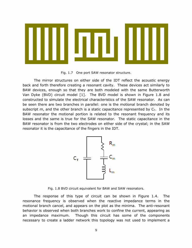
Fig. 1.7 One port SAW resonator structure.
The mirror structures on either side of the IDT reflect the acoustic energy back and forth therefore creating a resonant cavity. These devices act similarly to BAW devices, enough so that they are both modeled with the same Butterworth Van Dyke (BVD) circuit model [1]. The BVD model is shown in Figure 1.8 and constructed to simulate the electrical characteristics of the SAW resonator. As can be seen there are two branches in parallel: one is the motional branch denoted by subscript m, and the other branch is a static capacitance represented by CT. In the BAW resonator the motional portion is related to the resonant frequency and its losses and the same is true for the SAW resonator. The static capacitance in the BAW resonator is from the two electrodes on either side of the crystal; in the SAW resonator it is the capacitance of the fingers in the IDT.
Fig. 1.8 BVD circuit equivalent for BAW and SAW resonators.
The response of this type of circuit can be shown in Figure 1.4. The resonance frequency is observed when the reactive impedance terms in the motional branch cancel, and appears on the plot as the minima. The anti-resonant behavior is observed when both branches work to confine the current, appearing as an impedance maximum. Though this circuit has some of the components necessary to create a ladder network this topology was not used to implement a

10
bandpass filter until the early 1990’s [14]. Ikata, et al. detail a design procedure for using SAW resonator structures modeled as BVD circuits to be used in order to create bandpass filters. The topology used is shown in Figure 1.9.
Fig. 1.9 Bandpass ladder topology a) SAW circuit model b) single block.
Using this ladder network, Ikata, et. al. have shown that SAW devices can used to create a bandpass filter. Previous work has also shown that bandpass filters can be built using manufactured products [15]. This work also allows for the optimization of each individual component in order to meet the desired response. These off-the-shelf devices are typically made on quartz crystals which, by virtue of their small electromechanical coupling constant, K2, allows for only the design of small bandwidth filters. In order to optimize the topology for larger bandwidths it becomes necessary to custom-fabricate devices using piezoelectric substrates with larger values of K2, in this case lithium niobate.

11
1.5 Overview of Thesis
This thesis will develop all the necessary steps for modeling SAW resonators, designing an optimized ladder network using SAW resonators, and fabricating and testing the filter design. The goal of this thesis is to provide a systematic method of constructing optimized broadband bandpass filters based on SAW resonator technology. It should be emphasized that over the course of this work the understanding of both the underlying theory and the designs based on this theory evolved. This lead to a better understanding of how to create ladder networks based on optimized designs and process steps for fabricating SAW band pass filters. In addition a considerable amount of time was spent understanding the material properties of lithium niobate and the constraints these properties imposed on the fabrication process development. SAW bandpass filter topologies have been fabricated but no functional ladder networks were completely verified. The design and fabrication challenges will be discussed.
The thesis is organized as follows. Chapter 2 will show the development of the theory for SAW resonators, starting with the early work done by Datta et al., showing its shortcomings and the more recent COM theory which overcomes these shortcomings. This chapter ends with the description of BVD equivalent circuits. Chapter 3 describes ladder networks, how they are created with SAW resonators, and what is done to optimize the design. Chapter 4 gives a brief review of the history of early mask designs and what knowledge was gained from each design. This chapter also includes a detailed look at the fabrication process and ends with a description of the measurement techniques. Chapter 5 presents measured results, along with a discussion of these results. Chapter 6 reviews the understanding gained from this work and suggests future efforts that would overcome the problems encountered in this work and lead to functional custom-built optimized SAW broadband ladder filters fabricated on lithium niobate substrates.

12
Chapter 2
Theory of SAW Operation
2.1 Early Work and the Datta Model
Early work in modeling SAW devices by Datta focused on the evaluation of a single IDT structure [16]. These results can be applied to a variety of devices such as transversal filters and SAW resonator structures. In order to develop the model for an IDT structure, the structure must be quantified. Figure 2.1 shows a labeled IDT structure including, PI, the pitch of the electrodes, W, the aperture width of the device, and N, the number of finger pairs. An example of a resonator is shown in Figure 2.2 showing the distance between the reference planes of the IDT and the mirror as LG, the pitch of the mirror, PM, as well as the number of fingers in the mirror, NM. The thickness of the metal lines on the substrate, h, is not shown in either figure. As indicated in Figure 2.1, the width of the fingers and the spaces are equal to PI/4. All of these device parameters are summarized in Table 2.1.
Fig. 2.1 IDT structure with labeled physical dimensions.
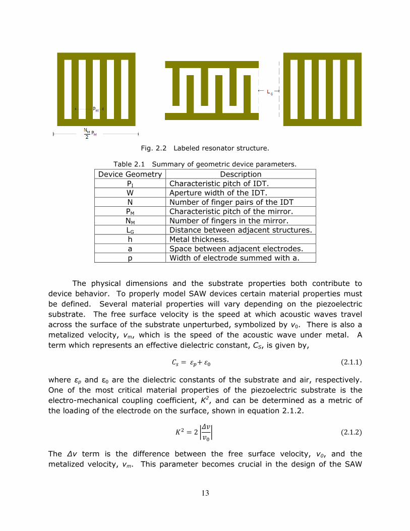
13
Fig. 2.2 Labeled resonator structure.
Table 2.1 Summary of geometric device parameters.
Device Geometry Description PI Characteristic pitch of IDT. W Aperture width of the IDT. N Number of finger pairs of the IDT PM Characteristic pitch of the mirror. NM Number of fingers in the mirror. LG Distance between adjacent structures. h Metal thickness. a Space between adjacent electrodes. p Width of electrode summed with a.
The physical dimensions and the substrate properties both contribute to device behavior. To properly model SAW devices certain material properties must be defined. Several material properties will vary depending on the piezoelectric substrate. The free surface velocity is the speed at which acoustic waves travel across the surface of the substrate unperturbed, symbolized by v0. There is also a metalized velocity, vm, which is the speed of the acoustic wave under metal. A term which represents an effective dielectric constant, CS, is given by, 2.1.1 where εp and ε0 are the dielectric constants of the substrate and air, respectively. One of the most critical material properties of the piezoelectric substrate is the electro-mechanical coupling coefficient, K2, and can be determined as a metric of the loading of the electrode on the surface, shown in equation 2.1.2.
2 2.1.2 The ∆v term is the difference between the free surface velocity, v0, and the metalized velocity, vm. This parameter becomes crucial in the design of the SAW

14
devices, in that it determines the maximum bandwidth achievable [15]. Another key material constant, Гs, is the ratio of K2/2 to Cs as shown by
Г 1 . 2.1.3 A list of material constants useful for modeling the IDT is given in Table 2.2. The values shown are all characteristic of a 128° rotated Y-cut, X-propagating, black lithium niobate crystal. Lithium niobate is the substrate material used throughout this work for reasons described in Chapter 4.
Table 2.2 Important material parameters. Expression Value Definition
v0 3996 [m/s] Free surface velocity
CS 5E-10 [F/m] Effective dielectric constant
K2 5.6% Electro-mechanical coupling coefficient
ΓS
5.6E7 [m/F] Defined relationship
A simplified model for a basic IDT structure was presented by Datta when these devices were introduced [16]. The IDT analyzed for this model has periodic electrodes that alternate between ground and the applied voltage. These structures are also analyzed with the length of the fingers running perpendicular to the acoustic wave propagation vector.
The IDT structure can be modeled by determining the relationship of the electrical stimulation to the acoustic wave front generated. This relationship can also work inversely, with an incident acoustic wave front and electrical output. Circuit elements can be used to model the acoustic behavior of the IDT device. The model is comprised of three distinct electrical components represented in Figure 2.3: the three components are: the capacitance due to the fingers, CT, the acoustic conductance, Ga(ω), and the acoustic susceptance, jBa(ω). It should be noted that it is assumed for the analysis, that effects due to the bus bars used to connect electrodes, and the resistance of the metal lines have been ignored.
The device feature that dominates this model is the pitch PI since it is directly related to the characteristic wavelength of the acoustic wave. This characteristic wavelength is related to the characteristic frequency of operation for the IDT which can be calculated to the first order from the free surface velocity, v0 as,
2.1.4

15
Fig. 2.3 Single IDT equivalent circuit.
If the charge distribution across each of the stimulated electrodes is considered to be uniform, the total capacitance is the superposition of the capacitance of each finger. The fringing field capacitance is considered to be insignificant assuming W and N are of appreciable size. An influential parameter in the calculation of this capacitance is the metallization ratio, η. This is defined as the distance between adjacent electrodes, a, divided by the width p. The total capacitance of the structure can then be written as in equation 2.1.6.
2.1.5 !" 2.1.6 " is a normalized capacitance value, and its value is dependent on η. For the case,
η = 0.5, this constant is equal to one. This is assumed to be the case for all work done.
This leaves the two acoustic portions of the circuit model to be evaluated. The conductance, Ga(ω), can be represented by the squared magnitude of the product of the Fourier transforms of the array factor and the charge distribution [16]. The array factor is a mathematical description of the voltage applied to the fingers of the IDT. The charge distribution is the description of the charge on each electrode. In order to arrive at this result a center frequency must be defined by
$% 2& . 2.1.7 For convenience the evaluation of the acoustic conductance can be shown in two parts, one that is frequency-independent and one that is not. The frequency-

16
independent portion is heavily dependent upon the physical geometry, including η
and can be written as Ga(Mωc), where is M represents the harmonic order.
()*$% *$% Г ()+" 2.1.8 The constant ()+" is equal to 2.871, and it should be noted that this number is only valid in the range of the first harmonic frequency. This constant varies for other harmonic orders, and values of η. The frequency-dependent portion of the conductance is a sinc function, whose argument is X, which is defined as,
- & $ . $%$% . 2.1.9 Only considering operation in the first harmonic of the device, the acoustic conductance can be written as,
()$ ()$% 0sin-- 4 . 2.1.10 The acoustic susceptance is directly related to the conductance through the Hilbert transform. This is obtained by convolving the expression for the conductance with 1/πf in the frequency domain. By evaluating this expression near the center frequency the susceptance can be approximated by,
6)$ ()$% sin2- . 2-2- . 2.1.11 An example of the acoustic contributions, Ga(ω) and Ba(ω), normalized by ()$%, is shown in Figure 2.4. The frequency and bandwidth of these responses vary with v0, N and PI. The acoustic contributions along with CT complete the IDT model. The admittance for an IDT is shown to be,
78$ ()$ 9 6)$ 9$ . 2.1.12

17
Fig. 2.4 Normalized acoustic conductance and susceptance plotted as functions of frequency.
In bandpass filter design, to meet specifications, ladder networks are required. Ladder networks consist of series and parallel components, each component being composed of inductors and capacitors. SAW resonator devices can be used in place of these components, to realize ladder networks. A SAW resonator is defined as a device containing at least one IDT in a resonant cavity. In order to realize a resonant cavity, two mirrors, long arrays of metal strips as shown in Figure 2.5, are used.
Fig. 2.5 Basic mirror structure with NM strips.
The basic premise of the mirror is that when a wave front generated by an IDT passes beneath a metal strip, a portion of the energy is reflected. When the wavelength of the acoustic wave is near PM, the mirror’s characteristic length, the

18
reflected waves add in phase. Passing beneath many strips, the amount of total reflected energy continues to grow. With an NM that is large, most of the energy is reflected back towards the IDT for acoustic wavelengths near PM. Two such mirrors, one on either side of an IDT, are able to contain the generated acoustic wave. This creates the resonant cavity, and the device known as the one-port SAW resonator shown in Figure 2.6.
Fig. 2.6 One-port SAW resonator device.
The mirror can be modeled as an acoustic transmission line, where each strip resembles a characteristic impedance mismatch [Reference 16, Ch. 6]. A transmission matrix can be used to relate the amplitudes of forward and reverse waves on the incident side to the amplitudes of forward and reverse waves on the exit side of the entire mirror as,
: ; <.< 1 =>? . 2.1.15
The term P2 is a phase term defined as,
@ABCDDE . 2.1.16 The reflectivity per electrode, r, is also frequency-dependent, and can be shown to be equal to,
< 9 F G2 HG IJ KLM & 2.1.17 where the piezoelectric coefficient, Pz, is -0.75 for η = 0.5. The mechanical coefficient, Fz, is based on properties of the substrate and the electrodes, and is given as,

19
HG .& NOPQP R OSR OGQG RT . 2.1.18 The Q properties can be calculated from the stress tensors of the substrate, ρ is the metal density, and c is a piezoelectric parameter with units Ǻ/V. The reflection of the mirror, R, can then be evaluated as,
U .VWV . 2.1.19 The effective velocity of the SAW is neither the free velocity, v0, nor the
metalized velocity, vm. In order to model the SAW resonator an effective velocity for the acoustic wave must be determined. The change of effective velocity, with respect to v0, can be written as,
. FX2 HX IJ . 2.1.20 Where Pv is the piezoelectric coefficient, equal to -1.5, for η = 0.5, and Fv is the mechanical loading given by,
HX 2 Y|OP|QP . R . [OS[R |OG|QG . R\ . 2.1.21 The values for the constants used in the velocity shift and reflectivity calculations are summarized in Table 2.3. Examples of calculating R are shown in Figure 2.7. It should be noted that the effective velocity was used to replace v0 to compute the characteristic frequency, f0, in Equation (2.1.4).
Table 2.3 Parameters for velocity and reflectivity calculations.
Material cx [Å/V] cy [Å/V] cz [Å/V] 128° rotated Y-cut lithium niobate 0.1 2.0 -1.2 ρ [kg/m3] QP [N/m2] QG [N/m2] Aluminum 2,695 2.5E10 7.8E10 Titanium 4,500 4.4E10 12.9E10 Gold 19,300 2.85E10 9.8E10

Fig. 2.7 Magnitude of reflection(blue line) b) N
The acoustic behavior of the SAW impedance [Reference 16, Ch. 10]the effective cavity length. effective distance of penetration into the mirrorfor LP is shown in equation structure to the effective penetrationgiven by equation 2.1.23. The lengths L and Lp are illustrated in Figure 2.6. length LC can be used in order to cawhich is defined in equation 2.1.24
The reflection coefficient for
20
Magnitude of reflection as a function of frequency normalized to f0 NM = 200 (red line) c) NM = 100 (green line)
e acoustic behavior of the SAW resonator can be expressed[Reference 16, Ch. 10]. An important feature of the SAW resonator is
the effective cavity length. In order to calculate the resonator’s cavity length theof penetration into the mirror, LP, must be known. equation 2.1.22. The distance from the center of the resonator
to the effective penetration depth of the mirror is defined as The lengths L and Lp are illustrated in Figure 2.6.
can be used in order to calculate the phase angle of the reflectivityequation 2.1.24.
one side of the resonator can be written as,
for a) NM = 400
can be expressed as electrical An important feature of the SAW resonator is
cavity length the . An expression
the center of the resonator of the mirror is defined as LC, and is
The lengths L and Lp are illustrated in Figure 2.6. The the reflectivity, θ,
one side of the resonator can be written as,

21
In order to determine the so-called motional impedance of the acoustic behavior it is necessary to include the interaction of the two mirrors and IDT. If it is assumed that 1) Ba(ω), the acoustic susceptance, can be ignored, and 2) there is no internal reflection due to the fingers of the IDT, Datta has shown that the impedance of the SAW resonator can be written as in equation 2.1.26. The subscripts ‘1’ and ‘2’ are used to distinguish the two mirrors. The total impedance of the SAW resonator is given by the motional impedance in parallel with CT.
] W^_` WAГaГbWc ГaWc Гb 2.1.26
Unfortunately the assumptions used to derive equation 2.1.26 lead to the prediction of artifacts in device behavior. Equation 2.1.26 predicts what are known as Fabry-Perot modes. The plot in Figure 2.9 shows the motional impedance in equation 2.1.26. The five anti-resonant peaks shown in the impedance are due to these Fabry-Perot modes. These modes are not always experienced by fabricated devices. They are a direct result of the two assumptions made. Coupling of Modes (COM) theory overcomes these artifacts.

Fig. 2.8 Magnitude of motional impedance, Z, plotted as a function of frequency showing f
22
Magnitude of motional impedance, Z, plotted as a function of frequency showing five Fabry-Perot anti-resonances.
Magnitude of motional impedance, Z, plotted as a function of normalized

23
2.2 Coupling of Modes Theory
Coupling of Modes (COM) theory can be applied to model a SAW resonator. In this theory, wave functions can be written to 1) relate the acoustic waves at different ports of the IDT, and 2) describe the transfer between electrical and acoustic wave energy in the IDT. Three ports in total are considered for the IDT: two acoustic ports and one electrical port. Hashimoto et al. [17] use the so-called p-matrix to describe the behavior of the IDT
deA0ecfgf h ;WW W WiW i.jWi .ji ii= ;
ec0eAfk = , 2.2.1 where j 2 with Vpeak, and j 4 with Vrms.
The two acoustic ports are taken at either side of the IDT. These are located at x = 0 and x = L. The distance L is the total length of the IDT. The terms, U(x)±, represent surface acoustic wave amplitudes where the subscripts ± indicate the direction of travel of the waves. The acoustic waves at the two acoustic ports are illustrated in Figure 2.9. The third port of the matrix is the electrical port which relates the applied voltage to the output current. The p-coefficients define relationships between the acoustic waves, the applied voltage, and the output current.
Fig. 2.9 Resonator showing both acoustic ports.

24
It is clear that p33 is the relation between voltage and current, and is the admittance of the IDT. Similar to the work by Datta, the acoustic admittance can be represented by its conductance, GI, and susceptance, BI. Since the device operates bi-directionally certain assumptions may be made about the coefficients. The assumptions not declared in equation 2.2.1 are, p22 = p11 and p23 = p13. . Furthermore, the assumption that the system is lossless leads to equation 2.2.2.
|WW| |W| 1 2.2.2 The governing differential equations that permit evaluation of the elements of the p-matrix, are given in equations 2.2.3 through 2.2.5.
mecnmn .9opecn . 9qWeAn 9rk 2.2.3 meAnmn 9qWecn . 9opeAn . 9rk 2.2.4 mgnmn .9jrecn . 9jreAn 9$k 2.2.5
These equations are solved using the boundary conditions inherent in equation 2.2.1. In order to express the solutions to these differential equations it is useful to define specific terms. The first term is the mutual coupling coefficient, κ12, which is related to the reflectivity per electrode by,
κW 2|r|Pv . 2.2.6 This relationship is derived by evaluating the COM model to match Datta’s model, with Ba(ω) = 0 and k12 of the IDT equal to zero. A capacitance per period, C, is also defined and is related to CS by,
. 2.2.7 Other useful definitions include the characteristic wave number, βu and the transconductance coefficient, ζ. These quantities along with several other definitions are shown in equations 2.2.9 and 2.2.10 [17].
wp 2& 2& 2.2.8 op wp . 2& x o yop . qW O

25
z o . opqW | rop qW 2.2.9 ~4!&j $ 2.2.10
With these relationships it is possible to solve for all of the p-coefficients using Fourier transformation analysis. Through rigorous algebra it is possible to derive expressions in terms of these quantities for the p-matrix elements as shown by Hashimoto et al..
WW z1 . @AB1 . z@AB 2.2.11 W @AB1 . z1 . z@AB 2.2.12 Wi |1 . z 1 . @AB1 z@AB 2.2.13 ii .29jr|f 1 . KLMO of2 1 z@BW z@ABW 9$f 2.2.14
These equations can fully describe the behavior of IDT. In the case of the mirror, the reflection factor, U-(0)/U+(0)=p11, can be obtained from the p-matrix with V = 0 (electrodes shorted together) and U-(L)=0 (no backward traveling acoustic wave beyond x=L). The evaluation of the reflected wave can be done by calculating the p11 with the mirror parameters. By defining the p11 of the mirror as Γr, the reflected waves can be written to include the phase shift induced by the distance between the mirror and IDT, LG, as,
z z@AB . 2.2.15 With these equations it is possible to model the admittance of a SAW resonator using,
7 ii 2jWiW WW . zAW . 2.2.16 The resonator admittance can also be rewritten in a few ways, all of which are equivalent. In order to accomplish this a few terms must be defined, which is done

in equations 2.2.17 through 2.2.19.re-written as shown in equation 2.2.20
These terms are useful for determining the resonant frequencies of the device. The resonant frequencies correspond to frequencies for which the denominator in equation 2.2.20 goes to zero. This occurs when,
with m being 0 or a positive or negative integer. Likewise, antifrequencies for which the numerator in equation 2.2.20 goes to zero, written as,
This allows for the modeling of the one portaccurate degree, as seen in Figurethe magnitude and phase of the impedance of the SAW resonator computed usingthe inverse of equation 2.2.20.
Fig. 2.10 SAW resonator impedance as a function of frequency computed from COM theory with PM = PI = 18 µm, N = 100,
26
in equations 2.2.17 through 2.2.19. The admittance of the resonator can then be written as shown in equation 2.2.20
These terms are useful for determining the resonant frequencies of the device. The correspond to frequencies for which the denominator in
equation 2.2.20 goes to zero. This occurs when,
being 0 or a positive or negative integer. Likewise, anti-resonances occur at frequencies for which the numerator in equation 2.2.20 goes to zero, written as,
This allows for the modeling of the one port SAW resonator to a more , as seen in Figures 2.10a and 2.10b. These figures show plots of
phase of the impedance of the SAW resonator computed usingequation 2.2.20.
mpedance as a function of frequency computed from COM theory = 100, W = 1000 µm, NM = 400, LG = 0: a) magnitude and b)
phase.
The admittance of the resonator can then be
These terms are useful for determining the resonant frequencies of the device. The correspond to frequencies for which the denominator in
resonances occur at frequencies for which the numerator in equation 2.2.20 goes to zero, written as,
resonator to a more These figures show plots of
phase of the impedance of the SAW resonator computed using
mpedance as a function of frequency computed from COM theory = 0: a) magnitude and b)

2.3 Suppressing Fabry Perot Resonances
As mentioned in Section 2.1, tevaluating a SAW resonator rIDT, and the acoustic susceptance, presented in the previous section, should converge to the same behavior as Datta, when these assumptions are applied. susceptance were set equal to zero in the COM model, done by Datta. Figure 2.11 shows that plots of the magnitude of the impedance as functions of frequency for the two models do in fact agree given these assumptions. The motional impedance for the COM model is obtained bsetting C=0 in Equation 2.2.14.
Fig. 2.11 Magnitude of motional impedance(blue), COM theory (red)
Setting the k12 of the IDT the acoustic conductance in the model. This is shown below in Figure 2.12shows plots of the magnitude of IDT k12.
27
Suppressing Fabry Perot Resonances
As mentioned in Section 2.1, the assumptions made by Datta when evaluating a SAW resonator were that the reflections from the fingers in the IDT
and the acoustic susceptance, Ba, were equal to zero. COM theory, as presented in the previous section, should converge to the same behavior as Datta, when these assumptions are applied. The coupling coefficient and the acoustical
re set equal to zero in the COM model, and then compared to work Figure 2.11 shows that plots of the magnitude of the
impedance as functions of frequency for the two models do in fact agree given The motional impedance for the COM model is obtained b
=0 in Equation 2.2.14.
otional impedance plotted as a function of frequency:(blue), COM theory (red) with Ba(ω)=0 and k12=0 for IDT.
of the IDT to more realistic values modifies the behavior ofthe acoustic conductance in the model. This is shown below in Figure 2.12shows plots of the magnitude of p33 as functions of frequency for different values of
he assumptions made by Datta when the reflections from the fingers in the IDT,
re equal to zero. COM theory, as presented in the previous section, should converge to the same behavior as Datta,
he coupling coefficient and the acoustical and then compared to work
Figure 2.11 shows that plots of the magnitude of the motional impedance as functions of frequency for the two models do in fact agree given
The motional impedance for the COM model is obtained by
plotted as a function of frequency: Datta
the behavior of the acoustic conductance in the model. This is shown below in Figure 2.12 which
as functions of frequency for different values of

Fig. 2.12 Real part of acoustic theory with k12PI of the IDT equal to
0.04 (red solid line)
The difference in acoustic conductance modifies the resonator behavior. The inclusion of the acoustic susceptance also impacts the nature of the motional impedance, as seen in Figure 2.13.the motional impedance as functions of frequency with with Ba(ω) not set equal to zer
28
Real part of acoustic conductance as a function of frequency compequal to a) 0.00 (blue solid line) b) 0.02 (blue dashed line)(red solid line) d) 0.08 (red dashed line).
The difference in acoustic conductance modifies the resonator behavior. The acoustic susceptance also impacts the nature of the motional
impedance, as seen in Figure 2.13. Figure 2.13 shows a plots of the magnitude of the motional impedance as functions of frequency with Ba(ω) set equal to zero and
not set equal to zero.
as a function of frequency computed from COM (blue dashed line) c)
The difference in acoustic conductance modifies the resonator behavior. The acoustic susceptance also impacts the nature of the motional
Figure 2.13 shows a plots of the magnitude of set equal to zero and

Fig. 2.13 Magnitude of motionacoustic susceptance set to zero
Together the two assumptions used in the Datta modelspectral response of the SAW resonator. 2.2.21 that Fabry-Perot modes through only one multiple of 2is appreciable. The region of mirror reflectivity is determined by the value of the mirror. The value of k12
reflectivity to be represented by the two vertical lines in FigSince the phase φ+(f) + φΓ(fthis region, a small enough absolute value of the slope would insure that this phase goes through a single multiple of 2this, as shown below.
29
otional impedance as function of frequency computed with set to zero (blue), and with acoustic susceptance not set to zero
two assumptions used in the Datta model drastically change the spectral response of the SAW resonator. In particular, it can be seen from equation
Perot modes will be suppressed if the phase φ+(fonly one multiple of 2π in the spectral region where the mirror reflectivity
The region of mirror reflectivity is determined by the value of
12 for the mirror is kept constant, allowing the region of reflectivity to be represented by the two vertical lines in Figures 2.14 and 2.15.
f) is approximately linear with respect to frequencya small enough absolute value of the slope would insure that this phase
goes through a single multiple of 2π. Modifying the k12 of the IDT accomplishes
as function of frequency computed with and with acoustic susceptance not set to zero (red).
drastically change the In particular, it can be seen from equation
f) + φΓ(f) goes rror reflectivity
The region of mirror reflectivity is determined by the value of k12 for for the mirror is kept constant, allowing the region of
ures 2.14 and 2.15. linear with respect to frequency in
a small enough absolute value of the slope would insure that this phase of the IDT accomplishes
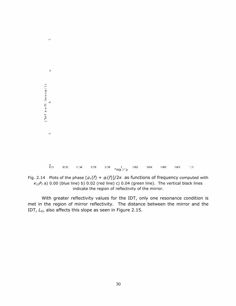
Fig. 2.14 Plots of the phase [φκ12PI a) 0.00 (blue line) b) 0.02
indicate the region of reflectivity
With greater reflectivity values for the IDT, only one resonance condition is met in the region of mirror reflectivity. The distance between the mirror and the IDT, LG, also affects this slope
30
φ+(f) + φΓ(f)]/2π as functions of frequencyb) 0.02 (red line) c) 0.04 (green line). The vertical black lines
indicate the region of reflectivity of the mirror.
With greater reflectivity values for the IDT, only one resonance condition is met in the region of mirror reflectivity. The distance between the mirror and the
fects this slope as seen in Figure 2.15.
as functions of frequency computed with
The vertical black lines
With greater reflectivity values for the IDT, only one resonance condition is met in the region of mirror reflectivity. The distance between the mirror and the

Fig. 2.15 Plots of the phase [φκ12 = 0.03 for both IDT and mirror and with
c) 0 (green line). The vertical black lines indicate the mirror region of reflectivity.
To minimize the possibility of Fabra result the device looks like a continuous structure to the acoustic wave fronwill suppress the Fabry-Perot modes, providing a more desired signal in the region of interest in the final device. Anthat suppresses unwanted Fabryresonator was designed with figure shows a plot of the magnitude of the impedance as a function of frequency
31
φ+(f) + φΓ(f)]/2π as functions of frequency= 0.03 for both IDT and mirror and with LG equal to a) 10PI (blue line) b)
The vertical black lines indicate the mirror region of reflectivity.
To minimize the possibility of Fabry-Perot modes the LG should be equal to zerohe device looks like a continuous structure to the acoustic wave fron
Perot modes, providing a more desired signal in the region of interest in the final device. An example of a SAW resonator designed in a way that suppresses unwanted Fabry-Perot modes is shown in Figure 2.16resonator was designed with LG = 0 and with κ12 ≈ 0.03 for the IDT and mirror. The figure shows a plot of the magnitude of the impedance as a function of frequency
as functions of frequency computed with b) 5PI (red line)
The vertical black lines indicate the mirror region of reflectivity.
should be equal to zero. As he device looks like a continuous structure to the acoustic wave front. This
Perot modes, providing a more desired signal in the region example of a SAW resonator designed in a way
16. The SAW for the IDT and mirror. The
figure shows a plot of the magnitude of the impedance as a function of frequency.

Fig. 2.16 Magnitude of SAW resonator
32
Magnitude of SAW resonator impedance using COM theory showing no FaPerot resonances.
impedance using COM theory showing no Fabry-

33
2.4 BVD Models for SAW Structures
While theoretical developments allow for an accurate description of a SAW resonator, the equations are cumbersome and slow to calculate. An equivalent circuit model is needed in order to simplify the model to permit quick simulation and circuit design. The use of the Butterworth Van Dyke circuit, as mentioned in Chapter 1, can be used to model the SAW resonator [Reference 16, Ch. 10]. An example of the circuit is repeated here for convenience in Figure 2.17.
Fig. 2.17 BVD circuit equivalent. The series circuit consisting of the elements Rm, Cm, and Lm is referred to as the “motional” branch of the BVD circuit.
In order to derive equations for the BVD device parameters in terms of SAW resonator parameters, the established theories must be approximated for frequencies near resonance. The Datta and COM models are expanded around resonance yielding two separate sets of equations for the BVD parameters. These are used to evaluate the impedance of the motional branch of the BVD circuit. The static capacitance, CT, is equivalent in both models.
In the work presented by Datta the resonator is described in the region around resonance considering a small change in frequency, ∆f [Reference 16, Ch 10]. By expanding equation 2.1.26 for a small frequency around resonance the motional impedance can be written as,
] 1() 1 . z 9z4&fW f/1 z . 2.4.1 This can be written in terms of electrical components as,
] U 94&f . 2.4.2 The motional resistance can be written as the real terms in equation 2.4.1 resulting in,

34
U 1()$% 1 . Г1 Г . 2.4.3
The value of Ga(ωc) is given by equation 2.1.8. The reflectivity of the mirror, Γ, given by equation 2.1.19, is evaluated at the center frequency resulting in,
|z| tanh |<| . 2.4.4 The reflectivity per electrode, r, is considered frequency independent with the sin term set equal to unity in equation 2.1.17. It can be seen from Equation 2.4.3 that the motional resistance is heavily influenced by h as well as NM. The higher NM, and the larger h, the more energy is reflected in the cavity. This results in values of Γ that are closer to unity and consequently to lower values of resistance.
In order to evaluate the motional inductance, Lm, the imaginary terms of equation 2.4.1 are evaluated with Γ ≈ 1 as,
f W^_`DE ac b 2.4.5 Lm is evaluated at resonance. The cavity lengths L1 and L2 are evaluated
using 2.1.23 with the penetration depth, Lp. The motional capacitance, Cm, is determined by the requirement that (2πf0)2=LmCm where f0 = vo/PI, resulting in,
14&f . 2.4.6 The evaluation of CT is given by equation 2.1.6. This completes the evaluation of the BVD circuit model based on the work presented by Datta.
Since Datta’s model has been shown to introduce artifacts, it is necessary to carry out the BVD circuit evaluation using COM theory. This is done similarly by expanding 2.2.16 around the center frequency. The capacitance per period, C, is set equal to zero, in order to evaluate only the motional branch of the circuit. The resulting expressions for the motional resistance and inductance are shown by,
U .9@B|7| 1 . |Γ|1 . |Γ|@B 12|7| 1 . |Γ|sin 2.4.7 and

35
f @B2&|7| |Γ|1 . |Γ|@B c´ ´ sin . 9@B´1 . |Γ| . 2.4.8
The prime notation is used to denote the first derivative with respect to frequency and the ‘R’ subscript is the evaluation of the term at the resonant frequency. The subscript “H” refers to component values evaluated using COM theory as expressed by Hashimoto. The phase angle, φI, and the admittance, YI, of the IDT are also evaluated with the static capacitance equal to zero. The motional capacitance term, CmH, is calculated from LmH by the requirement that (2πfrH)2=LmHCmH where frH is the COM resonant frequency.
These models show the BVD representation of a SAW resonator. It is important to note that the outcomes of these two models result in different impedances for the same device. For the same device the resistance predicted from COM theory is greater than that given by Datta. The frequency of resonance is also different in these two models. Through empirical results it can be shown that the motional resistance of the COM model is better suited for predicting device behavior using the BVD equivalent circuit. However, the equation for the motional inductance given by equation 2.4.5 yields a BVD equivalent circuit that better matches results computed using COM theory. This is because the inductance calculated using equation 2.4.8 includes derivatives evaluated at the resonant frequency. The imaginary part of the motional impedance at resonance often changes very rapidly with frequency, leading to a poor fit of the linear approximation for the frequency band over which the BVD model applies. Datta’s equation 2.4.5 is based on the frequency f0 which differs slightly from the true resonance, frH. It turns out that the imaginary part of the motional impedance computed from COM theory is more linear at f0 than it is at frH so that a better fit is obtained between the BVD equivalent circuit and the linear approximation of the COM model using Datta’s equation 2.4.5 to determine Lm and Cm. To summarize, an optimum fit between the BVD circuit and the impedance computed from the COM model is obtained using the motional inductance from the work by Datta (equation 2.4.5), and the resistance predicted by COM (equation 2.4.7). This model will be referred to as the “hybrid model” for the remainder of this work.

36
2.5 Diffraction Effects
The models presented in the previous sections take account of many factors to simulate device performance. These models do, however overlook some features which can affect the response of a resonator. Diffraction effects, determined by device size, can drastically change the effective motional resistance, and the impedance, of the device. The models developed assumed that the aperture of the device is so great that the wave front generated remains planar and does not diffract. In reality this is not the case, and due to the nature of resonant cavities can be a main contributor to loss. The diffracted wave front will make many trips across the cavity, losing energy each time. From optics theory [18] it can be shown that the diffraction angle of the wave front is approximated by,
o . 2.5.1 The term is the wavelength of interest and in the case of the SAW resonator is approximately equal to PI near resonance. With a large N the length of the total resonator device should be approximately equal to L, the product of N, the number of finger pairs, and, PI, the characteristic pitch. The lateral spread of the acoustic wave for a single pass through the resonator cavity due to diffraction is approximately equal to 2θL. After f2 passes through the resonator, the total width of the diffracted wavefront is approximately,
¡ 2of . 2.5.2 The term f2 in this instance represents a factor that must be empirically derived. Empirically the value of f was found to be approximately 7. In order to avoid diffraction effects, the aperture width, W, should be much larger than D. Setting the aperture width equal to D allows an expression to be written that relates W to N, PI, and the empirically derived factor f.
√2 . 2.5.3 This equation was used as an additional constraint in conjunction with the derived models, Sections 2.4, to ensure device functionality

37
Chapter 3
Design of Ladder Networks Using SAW
Devices
3.1 Discrete Element Ladder Networks
Discrete ladder networks are a useful tool in realizing desired filter performance. In order to understand the operation of the ladder network, it is easiest to start by analyzing a single block, replicated in Figure 3.1 for convenience.
Fig 3.1 Single block of a ladder network.
The impedance of this stage can be cascaded with that of other blocks. The subscript ‘ser’ is used to describe components of the series branch, and ‘par’ for the parallel. The single stage impedance is given by,
] 8)£¤ 9¥$f ¤ ¤f)) . $¥f ¤ ¤ f)) f) ¤¦ 1¦$if)) ¤ . $ ¤ . 3.1.1 Typically filters are characterized by their transfer functions. One particular transfer function is the voltage at the output, divided by the voltage at the input. The higher order filter functions have higher-order polynomials, and more blocks must be added for circuit implementation. An example of a bandpass filter built using ideal capacitors and inductors is shown in Figure 3.2.

Fig. 3.2 The frequency response
38
The frequency response 6th order elliptic filter approximation implemented with a 12 block ladder network.
approximation implemented with a

39
3.2 Ikata’s SAW Resonator Ladder Network
Ikata, et al. [14] have successfully explored the use of the BVD equivalent SAW model in ladder networks to realize bandpass filters. The interaction between the motional components and the shunt capacitor in the SAW resonator, see Figure 2.17, creates both a resonant and anti-resonant frequency. The motional resistance summarizes the energy loss in the system; therefore it does not affect the spectral characteristics of the ladder network. The basic ladder topology is shown below in Figure 3.3 with two components, the series and parallel BVD elements. For ease of analysis consider each of the series components, and each of the parallel components to be identical, such that there are only two unique BVDs.
Fig. 3.3 Bandpass Ladder Network with SAW BVD components.
The load and source resistance can be different from one another; however under normal circumstances they are equal. This is most beneficial when using a constant k-type approach, to filter design. The additional subscripts, ‘s’ and ‘p’, will signify if the component belongs to the series or the parallel BVD. In order for the filter to act as a proper bandpass, the anti-resonant frequency of the parallel device must coincide with the resonant frequency of the series device. This frequency also acts as the center frequency of the bandpass filter, ωc. A design parameter is Cr, the ratio of the shunt capacitor of the parallel device to the shunt capacitor of the series device. This will influence the out-of-band rejection and the pass band attenuation. The values of the shunt capacitors can be found directly using the constant k type approximation equation 3.2.2.
88 3.2.1 U 18 8$% 3.2.2
The center frequency, ωc, is given by filter specifications, and is equal to the geometric mean of the two passband frequencies, ωp1 and ωp2. The resonant

40
frequency of the parallel device, ωp1, should be chosen to accommodate fabrication capabilities. The second pass band frequency, ωp2, can then be calculated. These values can be used to determine the values of the individual components of the BVD. Equations 3.2.3 and 3.2.4 express the resonant and anti-resonant frequencies of the BVD circuit, respectively. The difference between the squares of these frequencies can be rewritten conveniently as equation 3.2.5. Subscripts ‘s’ and ‘p’ have been omitted in Equations 3.2.3-3.3.5 since these equations apply to both series and parallel BVD circuits. The values of the shunt capacitors are known, therefore only the motional inductances are left to be calculated.
$ 1f 3.2.3 $) 1f 18 1 3.2.4 $) . $ 1f8 3.2.5
This design procedure is not the only filter expression that can be realized with this topology. Ladder networks in general are capable of expressing a multitude of filter approximations, however this one is reviewed in detail because of its popularity with the one-port SAW resonator devices. An example of this design approach is shown in Figure 3.4. Previous work has shown that it is possible to assemble these types of filters using commercially available SAW resonators [15].

Fig. 3.4 Frequency response of SAW resonator ladder network based on a transfer function using constant k
This approximation is not best suited to all applications of analog filters. In particular, large bandwidth filters may be desired. These cannot be achieved with commercially available SAW devices. In order to tailor tresonator separately, custom fabrication is required. The substrate used is critical to the bandwidth achievable Mass-manufactured SAW resonator devices are fabricated almost exclusively on quartz which has a relatively low value for bandwidth filters, it was necessary to customSAW resonators with larger values of lithium niobate was selected mainly because of its larger
41
Fig. 3.4 Frequency response of SAW resonator ladder network based on a transfer function k design; fc = 221 MHz, B = 9.5 MHz, Cr = 2.0.
This approximation is not best suited to all applications of analog filters. In large bandwidth filters may be desired. These cannot be achieved with
commercially available SAW devices. In order to tailor the impedance of each SAW resonator separately, custom fabrication is required. The substrate used is critical to the bandwidth achievable [15], and will be discussed in detail in Chapter 4.
manufactured SAW resonator devices are fabricated almost exclusively on quartz which has a relatively low value for K2. Therefore, in order to achieve larger
th filters, it was necessary to custom-fabricate ladder networks based on ith larger values of K2. In this thesis 128° rotated Y
lithium niobate was selected mainly because of its larger K2 value.
Fig. 3.4 Frequency response of SAW resonator ladder network based on a transfer function
= 2.0.
This approximation is not best suited to all applications of analog filters. In large bandwidth filters may be desired. These cannot be achieved with
he impedance of each SAW resonator separately, custom fabrication is required. The substrate used is critical
d in detail in Chapter 4. manufactured SAW resonator devices are fabricated almost exclusively on
. Therefore, in order to achieve larger fabricate ladder networks based on
. In this thesis 128° rotated Y-cut black

42
3.3 Systematic Design Approach for Realizing a Bandpass Filter Approximation Using a SAW Ladder Network
When evaluating a SAW resonator for filter performance it is important to have an accurate description of the frequency behavior. This allows for the passband to be realized. Modeling the energy loss in the resonator with the motional resistance is a difficult task since this term is also frequency-dependent. The insertion loss of the filter topology, which is a critical parameter in filter specifications, depends ultimately on the motional resistance. By applying the hybrid model, described in Section 2.4, an adequate fit is calculated.
A sixth-order elliptic filter function can be synthesized based on desired spectral specifications. An important caveat is that specifications such as the passband frequencies must be compatible with the available lithography process. Using a simulation tool with an optimization routine, the synthesized function can be the target for the transfer function of SAW-based ladder network. In order to obtain an accurate response over the desired range of frequencies, the optimization routine used is the least-square quadratic, LSQ, method. This method measures the error between the actual transfer function and the target. The simulator adjusts the design variables until the lowest error is found. When this iterative process is complete the curve obtained will be the best fit to the target transfer function. This is not as straightforward as it seems, however; each program has its own subtleties that need to be accounted for in order to obtain the desired result. The exact process used for simulation is detailed in Appendix A.2.
Previous work has been done using this optimization routine to build ladder networks based on quartz SAW resonators [15]. It is important to examine the differences in the process used in this thesis compared to the previous work. One important difference is that the number of degrees of freedom has been changed. The previous work used the BVD model based on the theory of Datta which resulted in three degrees of freedom: N, W, and LG. This work did not account for the Fabry-Perot resonances, therefore the same degrees of freedom cannot be used with the hybrid model.
In order to suppress the Fabry-Perot resonances, LG, defined in Section 2.1, is forced to zero, removing one degree of freedom. For accurate device functionality the effects of diffraction should also be considered which links W to N, as shown in Section 2.5. This means that that the factor f described in Section 2.5 should be set empirically, by creating test structures, leaving only N to vary. The bounds of N must also be set, with a lower bound of N =10, and an upper bound of N = 800. The lower bound was chosen since IDTs with N less than 10 have shown poor response during initial work. Since W is dependent on N, the upper bound is chosen because of device area considerations. Using this method it is possible to

generate a bandpass filter function, as seen below in Figure 3.5. parameters are specified in Table 3.1 and 3.2
Fig. 3.5 Results of LSQ optimization routine using
Table 3.1 Target elliptic function parameters.
Table 3.2 Optimized hybrid model parameters.DeviceS1S2S3P1P2P3
43
generate a bandpass filter function, as seen below in Figure 3.5. Target and result meters are specified in Table 3.1 and 3.2, respectively.
Results of LSQ optimization routine using the hybrid model.
Table 3.1 Target elliptic function parameters. Specification Value
n 6 αp -0.5 αs -20.0 fc 221.0 MHz B 9.5 MHz
3.2 Optimized hybrid model parameters. Device PI [µm] W [µm] N S1 17.6 3643 437 S2 17.6 3940 511 S3 17.6 4076 547 P1 18.0 1981 124 P2 18.0 2261 161 P3 18.0 3468 379
Target and result
hybrid model.
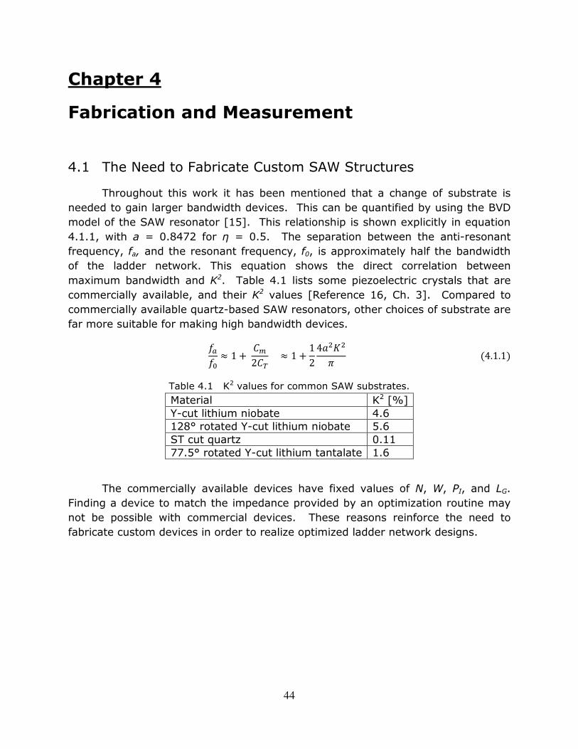
44
Chapter 4
Fabrication and Measurement
4.1 The Need to Fabricate Custom SAW Structures
Throughout this work it has been mentioned that a change of substrate is needed to gain larger bandwidth devices. This can be quantified by using the BVD model of the SAW resonator [15]. This relationship is shown explicitly in equation 4.1.1, with a = 0.8472 for η = 0.5. The separation between the anti-resonant frequency, fa, and the resonant frequency, f0, is approximately half the bandwidth of the ladder network. This equation shows the direct correlation between maximum bandwidth and K2. Table 4.1 lists some piezoelectric crystals that are commercially available, and their K2 values [Reference 16, Ch. 3]. Compared to commercially available quartz-based SAW resonators, other choices of substrate are far more suitable for making high bandwidth devices.
) 1 2 1 124& 4.1.1 Table 4.1 K2 values for common SAW substrates. Material K2 [%] Y-cut lithium niobate 4.6 128° rotated Y-cut lithium niobate 5.6 ST cut quartz 0.11 77.5° rotated Y-cut lithium tantalate 1.6
The commercially available devices have fixed values of N, W, PI, and LG. Finding a device to match the impedance provided by an optimization routine may not be possible with commercial devices. These reasons reinforce the need to fabricate custom devices in order to realize optimized ladder network designs.

45
4.2 SAW Test Structure Evolution and Summary of Mask Sets
There are many options when fabricating the device that are not included in the theory of their operation. For example, the actual design of masks must incorporate other features such as probe pads. There were a total of five masks created in order to develop better design procedures for fabricating SAW resonator structures. Table 4.2 details the main structures on each of the masks and the reasons for fabrication.
Table 4.2 Overview of masks used to design SAW resonator based ladder networks. Mask Name Features Reasoning Kenai SAW resonator, one- and two-
port measurement. Modeling and measurement confirmation
Agulapak SAW resonator two-port measurement
Determining grounding schemes for device measurement
Optimator Optimized SAW-based ladder Build optimized ladder network OptimatorM Isolated resonators from
Optimator design Determine cause for undesired responses in Optimator devices
OptimatorF Optimized ladder network and SAW resonator components
Build optimized ladder network based on results of OptimatorM
The first mask, Kenai, was fabricated to determine the best way to measure the resonant structures. It was determined that using two ports to measure the resonator gave the most consistent and reliable data. The anti-resonant frequency was observed closer to the resonance frequency than expected. It was noted, post-fabrication, that the mirrors were connected to the ground pads on this mask. Agulapak was designed to determine whether this grounding had an effect on device performance. The Optimator mask was the first attempt at fabricating an optimized ladder network. The final two masks gave more understanding into the nature of the devices, and will be discussed in detail in the next section.

46
4.3 Test Structures for Components and Complete Ladder Networks
This section discusses the last two masks to be fabricated in greater detail. These masks are critical in understanding the device functionality and design guidelines for SAW resonators. The first mask, OptimatorM, includes the devices with the dimensions listed in Table 4.3. It also should be noted that for both the masks covered in this section, the value of NM, the number of fingers in the mirror, is 400.
Table 4.3 Device sizes on OptimatorM. Device PI [µm] W [µm] N S1 17.6 115 464 S2 17.6 50 528 S3 17.6 50 499 P1 18.0 1000 32 P2 18.0 1000 32 P3 18.0 50 546

47
Fig. 4.1 OptimatorM resonator device structures a) reduced ground trace pattern b) conventional ground trace pattern
Devices from the OptimatorM mask were fabricated in more than one way. Figure 4.1 shows the two different constructions of the devices. The device shown in Figure 4.1 a) has the ground lines connecting to either side of the mirror with no metal running around the mirror. The device in 4.1 b) shows the mirrors grounded in the same fashion, with an additional metal line running around the mirrors. A picture of a fabricated P1 device is shown in Figure 4.2. Theory suggests that with enough mirror strips most of the energy should be confined to the cavity. Therefore the additional metal line should not have any significant impact on device functionality. When fabricating a full ladder network, using a single layer of metal, it becomes necessary to run metal lines around the mirror. By comparing these designs directly it could be determined if this has significant impact on the device performance.
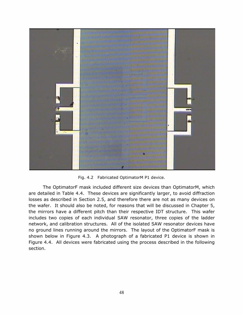
48
Fig. 4.2 Fabricated OptimatorM P1 device.
The OptimatorF mask included different size devices than OptimatorM, which are detailed in Table 4.4. These devices are significantly larger, to avoid diffraction losses as described in Section 2.5, and therefore there are not as many devices on the wafer. It should also be noted, for reasons that will be discussed in Chapter 5, the mirrors have a different pitch than their respective IDT structure. This wafer includes two copies of each individual SAW resonator, three copies of the ladder network, and calibration structures. All of the isolated SAW resonator devices have no ground lines running around the mirrors. The layout of the OptimatorF mask is shown below in Figure 4.3. A photograph of a fabricated P1 device is shown in Figure 4.4. All devices were fabricated using the process described in the following section.
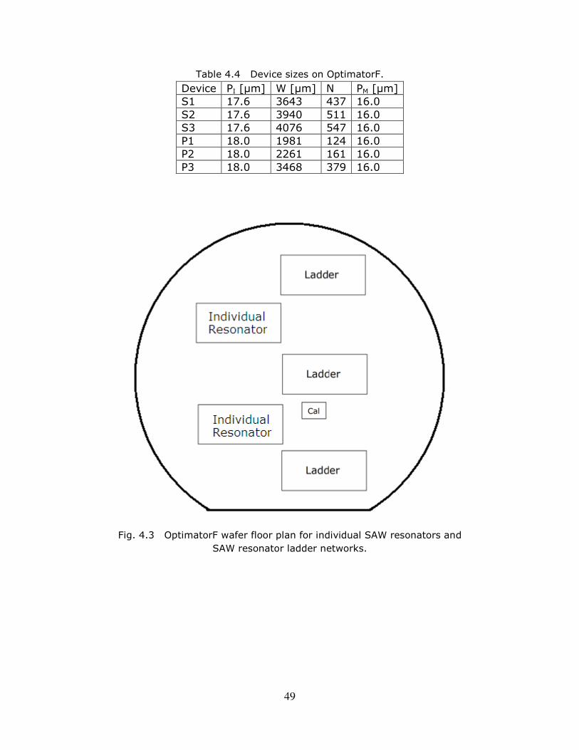
49
Table 4.4 Device sizes on OptimatorF. Device PI [µm] W [µm] N PM [µm] S1 17.6 3643 437 16.0 S2 17.6 3940 511 16.0 S3 17.6 4076 547 16.0 P1 18.0 1981 124 16.0 P2 18.0 2261 161 16.0 P3 18.0 3468 379 16.0
Fig. 4.3 OptimatorF wafer floor plan for individual SAW resonators and SAW resonator ladder networks.

50
Fig. 4.4 Fabricated OptimatorF device P1.

51
4.4 SAW Fabrication Development and Definition
The fabrication of the SAW devices makes use of well-established semiconductor manufacturing technology. By defining metal lines on the surface of a piezoelectric substrate it is possible to fabricate SAW devices. From a design perspective the first choice to make is which substrate to utilize. As mentioned earlier, the choice of substrate is 128° rotated Y-cut, X-propagating black lithium niobate, manufactured by Crystal Technologies, Inc. in Palo Alto, California. There are many desirable features to this substrate. First and foremost is the orientation and cut of the crystal. The propagation direction ensures that the propagation of the acoustic wave front is completely confined to the surface which is perpendicular to the flat of the wafer. There are however, undesired features of this substrate. Lithium niobate is also what is known as a pyroelectric material. This means a change in temperature causes a charge to build up in the crystal lattice. While heating, which occurs during many of the processes, the wafer has a probability to shatter if enough charge is built up. The term “black” refers to a chemically reduced version of the crystal, which greatly reduces this effect. Even using the black substrate this effect is still present however. The methods of fabrication chosen are intended to reduce any chance of shattering.
The periodic gratings used to form the IDT and mirror structures can be realized by either using metal or by etching into the wafer. Aluminum metallization allows the fabrication process to be accomplished with one mask. This provides a process simpler than etching the substrate. Compared to other metals aluminum is relatively easy to etch, inexpensive, and the process tools are well-calibrated. Lift-off photolithography is another technique that can be used to define the metal lines; however, the temperatures required to cure the photoresist are much higher, adding significant risk of substrate shattering.
The first step in fabrication of the SAW structures was an aluminum evaporation process, accomplished in the CVC Evaporator. The tool pumped the substrate down to hi-vac levels, approximately 0.4 µTorr, and used a tungsten basket with a source pellet of 99.99% Al, 0.01% Si. Current was passed through the tungsten basket until enough heat was transferred to the source, which causes sublimation to occur. In order to accurately predict the effects of metal thickness on device operation, the target thickness of the metal should be less than 1% of PI, the IDT pitch. Therefore the target thickness for the aluminum layer was 1500 Å. This thickness also allowed for non-destructive probing. Aluminum was deposited on the backside of the wafer in order to provide a ground path for any charge built up during subsequent processing. While a thicker metal layer would result in better ground connections, it would require more etch time, causing the masked lines on the front side to be over-etched. Other methods of depositing metals onto

52
substrates, such as sputtering techniques, tend to heat the substrate to high temperatures which could shatter the wafer.
Following the aluminum deposition a photolithographic step was required to mask the wafer for etching. Conventional recipes for photoresist processing and automated tools present multiple problems for processing. The photoresist used for this process was OCG Microelectronic Materials, HPR 504. Even though the “black” wafer choice is more opaque than the non reduced wafers, the automated track and stepper tools use optical recognition, and are not always able to find wafers. This is because the wafer is still somewhat transparent. The thermal sensitivity also requires all the necessary bakes to be modified. This means the maximum bake temperature had to be at the low end of the manufacturer recommendations, which resulted in longer bake times. It is suggested by Crystal Technologies, Inc. that black lithium niobate be subjected to temperature changes no greater than 1°C per minute. This process becomes very time-consuming and it is critical that wafer handlers used to remove the substrates are warmed to the same temperature as the wafer. In order to process the photoresist without shattering, the thermal recipes in Table 4.5 are used. The manual spin recipes for the CEE Spin Coater are used to obtain 1 µm of photoresist, and can be found in Table 4.6.
Table 4.5 Thermal Steps for photoresist processing. Step Temperature [°C] Time [min]
HMDS – Initial 60 1
Ramp 5 per minute 2
Bake 70 5
Cool -5 per minute >2
Soft Bake – Initial 60 1
Ramp 5 per minute 2
Bake 90 2
Cool -5 per minute >6
Hard Bake- Initial 60 1
Ramp 5 per minute 2
Bake 115 5
Cool -5 per minute >11
Table 4.6 Spin recipe for CEE Spin Coater. Step RPM Time [sec]
Ramp 100 per second 3
Spin 300 3
Ramp 2000 per second 2.35
Spin 5000 60
Decelerate -- --
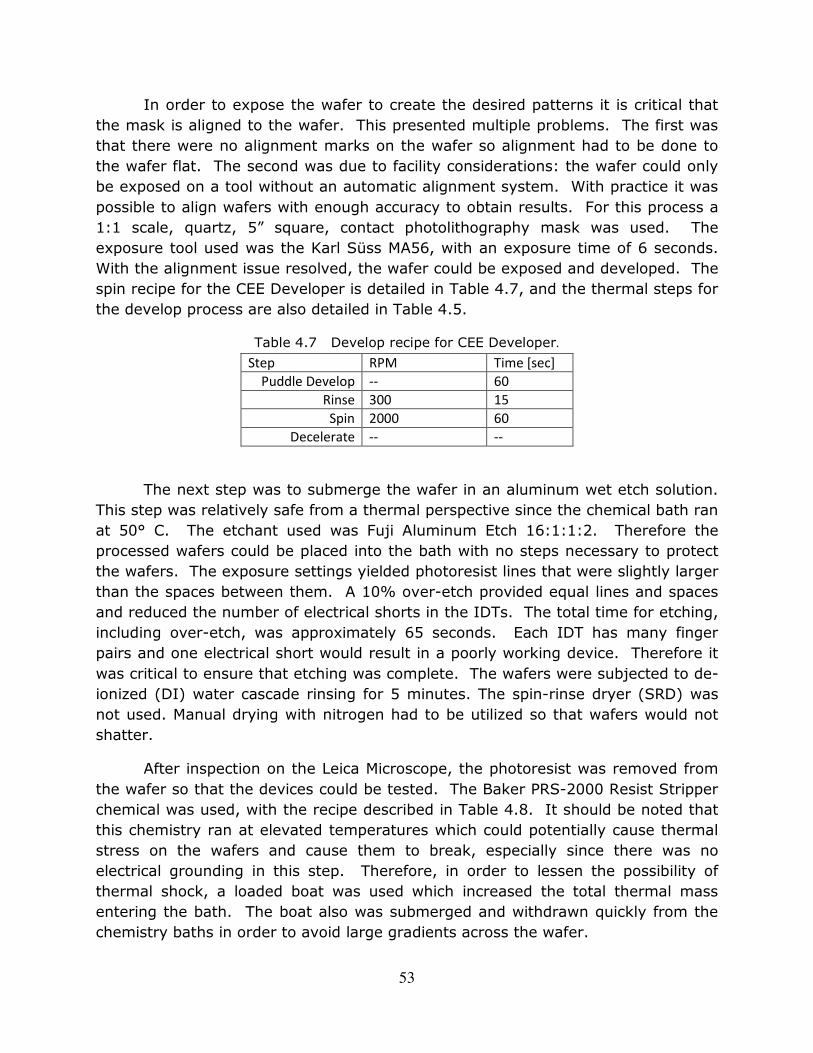
53
In order to expose the wafer to create the desired patterns it is critical that the mask is aligned to the wafer. This presented multiple problems. The first was that there were no alignment marks on the wafer so alignment had to be done to the wafer flat. The second was due to facility considerations: the wafer could only be exposed on a tool without an automatic alignment system. With practice it was possible to align wafers with enough accuracy to obtain results. For this process a 1:1 scale, quartz, 5” square, contact photolithography mask was used. The exposure tool used was the Karl Süss MA56, with an exposure time of 6 seconds. With the alignment issue resolved, the wafer could be exposed and developed. The spin recipe for the CEE Developer is detailed in Table 4.7, and the thermal steps for the develop process are also detailed in Table 4.5.
Table 4.7 Develop recipe for CEE Developer.
Step RPM Time [sec]
Puddle Develop -- 60
Rinse 300 15
Spin 2000 60
Decelerate -- --
The next step was to submerge the wafer in an aluminum wet etch solution. This step was relatively safe from a thermal perspective since the chemical bath ran at 50° C. The etchant used was Fuji Aluminum Etch 16:1:1:2. Therefore the processed wafers could be placed into the bath with no steps necessary to protect the wafers. The exposure settings yielded photoresist lines that were slightly larger than the spaces between them. A 10% over-etch provided equal lines and spaces and reduced the number of electrical shorts in the IDTs. The total time for etching, including over-etch, was approximately 65 seconds. Each IDT has many finger pairs and one electrical short would result in a poorly working device. Therefore it was critical to ensure that etching was complete. The wafers were subjected to de-ionized (DI) water cascade rinsing for 5 minutes. The spin-rinse dryer (SRD) was not used. Manual drying with nitrogen had to be utilized so that wafers would not shatter.
After inspection on the Leica Microscope, the photoresist was removed from the wafer so that the devices could be tested. The Baker PRS-2000 Resist Stripper chemical was used, with the recipe described in Table 4.8. It should be noted that this chemistry ran at elevated temperatures which could potentially cause thermal stress on the wafers and cause them to break, especially since there was no electrical grounding in this step. Therefore, in order to lessen the possibility of thermal shock, a loaded boat was used which increased the total thermal mass entering the bath. The boat also was submerged and withdrawn quickly from the chemistry baths in order to avoid large gradients across the wafer.
54
Table 4.8 Photoresist strip recipe. Tank Temperature [°C] Time [min]
PRS-2000 1 90 5
PRS-2000 2 90 5
Rinse Room 5
After the photoresist was completely stripped off the front of the wafer, the devices were ready to test. Additional measurements were made at this point to determine the actual height of the metal. This process could only be done with designs that have probe pads designed in the same layer as the devices. This allowed the process to remain simple, inexpensive, and relatively safe from wafer shattering.

55
4.5 Measurement Techniques
Analog filtering is utilized in many systems. These systems usually require connections using coax cable. These cables have characteristic impedance, Z0, and a common standard value of Z0 is 50 ohms. Therefore in order to connect these cables to the SAW devices, ground and signal paths are required on the SAW devices. The layouts were created to include probing by a ground – signal – ground (GSG) configuration. This means that there are three probe heads per port, the two outside pads for ground and the center pad for the signal. In order to characterize these devices an Agilent Technologies E5071C Network Analyzer was used to obtain electrical measurements.
This process required a full two-port calibration, including open, short, through, and load measurements. This was accomplished with calibration structures designed on chip, or by using an external calibration standard. For the measurements taken the calibration standard was used. The reasons for this are detailed in Appendix A.3. Settings of the network analyzer which ensured good response characteristics are described in detail in Appendix A.3. The evaluation of the characteristics of SAW devices was accomplished by measuring electrical impedance. The network analyzer, however, measures directly what are known as S parameters. These are related to the impedance of the network and can be used to determine the impedance of the device under test (DUT). In order to determine the impedance, it is necessary to measure both the magnitude and phase of the S parameters. In order to maneuver between the two metrics it becomes important to understand the meaning of the S parameters. The relationship between S parameters and impedance is also discussed in Appendix A.3.
56
Chapter 5
Experimental Results
5.1 Early Results
The first mask fabricated was Kenai. The purpose of this mask was to determine how the devices should be measured and to verify the model for device behavior. Results showed devices measured using two ports were less susceptible to measurement uncertainty. On this mask one side of the IDT was connected to the mirrors, which were in turn tied to the ground pads. However, it was unclear from testing results whether or not the mirror structures should have been tied to the ground pads. Theory suggests that if the mirror strips are shorted together no charge should build on the metal. The measured results showed the predicted resonant frequencies. The magnitude of impedance and anti-resonant frequencies did not match theory. The narrower bandwidth suggested that the static capacitance, CT, was larger than predicted. The grounded mirrors were suspect to causing this increase in capacitance.
The next mask fabricated was Agulapak, which included devices with mirrors that were connected to the ground ports and mirrors that were floating. The response of these devices showed better matching to theory when the mirrors were tied to the ground pads. All of these devices used two sets of GSG probe pads for testing. The metal layer was of poor quality, resulting in many shorts and opens. The responses suggested that the resonant and anti-resonant frequencies were realized, although the impedance excursion was small. This lead to the belief that the model was correct and better fabrication would yield functional devices.
The next mask, Optimator, used the optimization routines discussed in Section 3.3 to design SAW resonator based ladder networks. The individual devices are identical to the ones listed for OptimatorM in Table 4.3. Unfortunately, none of the ladder networks on this mask performed properly. The mask only included full ladder networks without the capability of testing isolated components. In order to determine the exact cause of the failure of the ladder networks, each of the devices needed to be examined closely. These results lead to the development of the final two masks.

57
5.2 Undesirable Effects Due to Low Acoustic Reflectivity and Diffraction
The OptimatorM mask allowed for the testing of the individual components in the ladder networks included in Optimator. Many insights about device operation and the approximations determining device parameters were gained. The first outcome of this mask, and the least critical, was that better responses can be realized if there are no metal lines around the mirrors. This might be expected since the metal line around the mirror can only interfere with device performance. Therefore only the devices without metal lines around the mirrors were considered. In order to fully understand other results obtained from the devices fabricated with OptimatorM, it is important to talk about the operation of different devices in detail. For convenience the device sizes are shown again in Table 5.1.
Table 5.1 Device sizes on OptimatorM.
Device PI [µm] W [µm] N S1 17.6 115 464 S2 17.6 50 528 S3 17.6 50 499 P1 18.0 1000 32 P2 18.0 1000 32 P3 18.0 50 546
The first devices to be examined are P1 and P2, which have identical properties. These devices were the best performing from this mask set. The measured impedance of these devices is shown below in Figures 5.1a) and 5.1b). The impedance was obtained from measured values of S11 according to the methods described in Appendix A.3. At first it appears that the response has two separate anti-resonant responses. This is not predicted by the hybrid model which is used to generate the device sizes in the optimization routine.

Fig. 5.1 Measured impedance of P1 and P2 devices, a) magnitude b) phase.
The ‘secondary’ anti-resonant response, which othan the anti-resonant response, can be accurately predicted with COM theory. The overlay of the measured data 5.2b). It should be noted that in order for COM theory to match the measured data additional resistance needs to be added to the computed motional resistance. This is reasonable considering that due to misalignment, are not accounted for in COM theory. The additional spike in impedance is apparently due to the low reflectivity of the mirrors. This spike can be suppressed if higher values of reflectiadditional spike severely impacts the operation of the device as well as any ladder networks using this device.
Fig 5.2 Measured P1 P2 impedance compared to COM predicted behavior, a) magnitude
The other devices on the mask all have many fingers with relatively small aperture widths. This introduces a different problem to the device operation. The
58
impedance of P1 and P2 devices, a) magnitude b) phase.
resonant response, which occurs at a lower frequency resonant response, can be accurately predicted with COM theory. The
overlay of the measured data and COM theory is shown below in Figures 5.2a. It should be noted that in order for COM theory to match the measured data
additional resistance needs to be added to the computed motional resistance. This that the resistances of the metal lines, as well as any loss
are not accounted for in COM theory. The additional spike in impedance is apparently due to the low reflectivity of the mirrors. This spike can be suppressed if higher values of reflectivity are assumed in COM theory. This additional spike severely impacts the operation of the device as well as any ladder
Measured P1 P2 impedance compared to COM predicted behavior, a) magnitudeb) phase.
The other devices on the mask all have many fingers with relatively small aperture widths. This introduces a different problem to the device operation. The
impedance of P1 and P2 devices, a) magnitude b) phase.
ccurs at a lower frequency resonant response, can be accurately predicted with COM theory. The
and COM theory is shown below in Figures 5.2a) and . It should be noted that in order for COM theory to match the measured data
additional resistance needs to be added to the computed motional resistance. This stances of the metal lines, as well as any loss
are not accounted for in COM theory. The additional spike in impedance is apparently due to the low reflectivity of the mirrors. This spike can be
vity are assumed in COM theory. This additional spike severely impacts the operation of the device as well as any ladder
Measured P1 P2 impedance compared to COM predicted behavior, a) magnitude
The other devices on the mask all have many fingers with relatively small aperture widths. This introduces a different problem to the device operation. The

aperture width is so small thatSection 2.5). These effects can be simulated with a much higher motional resistance in the BVD model or an additional resistance in series with the device. The measured impedance of device S2 illustrating the losses due to diffraction is shown in Figures 5.3a) and 5.3bW derived in Section 2.5, was basedconstraint insures that diffraction losses will be minimized.
Fig 5.3 Measured S2 impedance compared to COM pr
59
that a lot of loss is incurred due to diffraction effects (see 2.5). These effects can be simulated with a much higher motional
resistance in the BVD model or an additional resistance in series with the device. The measured impedance of device S2 illustrating the losses due to diffraction is
nd 5.3b). The semi-empirical relationship between derived in Section 2.5, was based in part upon these observations. This design
constraint insures that diffraction losses will be minimized.
g 5.3 Measured S2 impedance compared to COM predicted behavior, a) magnitudeb) phase.
a lot of loss is incurred due to diffraction effects (see 2.5). These effects can be simulated with a much higher motional
resistance in the BVD model or an additional resistance in series with the device. The measured impedance of device S2 illustrating the losses due to diffraction is
empirical relationship between N and in part upon these observations. This design
edicted behavior, a) magnitude

60
5.3 Undesirable Effects of Parasitics and Large Area Devices
The purpose of the final mask, OptimatorF, was to integrate all of the knowledge gained until this point. Fewer degrees of freedom available for optimizing the ladder network due to the additional constraint placed on N and W mentioned in Section 5.2. The optimization routine was run using these constraints, to match the target described in Table 3.1, to determine device parameters. Furthermore, in order to reduce the undesired spike, the pitch of the mirror was shifted from that of IDT. These remedies will be discussed in this section.
Unfortunately the measured results for the individual resonators on this mask did not show good matching to theory. The resonant and anti-resonance points were far different than predicted, which was not seen previously in any other devices. Each device in this mask needed to be examined closely in order to determine the reason for each device failure. For convenience the device sizes are repeated in Table 5.2.
Table 5.2 Device sizes on OptimatorF.
Device PI [µm] W [µm] N PM [µm] S1 17.6 3643 437 16.0 S2 17.6 3940 511 16.0 S3 17.6 4076 547 16.0 P1 18.0 1981 124 16.0 P2 18.0 2261 161 16.0 P3 18.0 3468 379 16.0
In general it can be seen that the parallel devices are smaller than the series components. The measured impedances of the parallel devices have anti-resonant peaks which sit very close to the resonant point. The measured impedance of device P1 compared to COM is shown in Figure 5.4a) and 5.4b). The resonant frequency of these devices does not correlate to the expected value based on PI. In order to determine why this had been the case a new model to include multiple parasites must be used.

Fig. 5.4 Overlay of the measured impedance and COM model impedance for device P1
In order to understand why the measured impedance spectra do not agree with theoretical impedances computed from the COM model, it important to realize that the COM results do not include the effects of parasitics. The impedance measured by the network anpad and the bus bar on both sides of the device as well as four parasitic capacitances surrounding the IDT structure, which can be reduced to one capacitance in parallel. Figure 5.5
61
Overlay of the measured impedance and COM model impedance for device P1a) magnitude b) phase.
In order to understand why the measured impedance spectra do not agree with theoretical impedances computed from the COM model, it important to realize that the COM results do not include the effects of parasitics. The impedance measured by the network analyzer includes the parasitic resistance between the pad and the bus bar on both sides of the device as well as four parasitic capacitances surrounding the IDT structure, which can be reduced to one
Figure 5.5 shows each of these parasitics.
Overlay of the measured impedance and COM model impedance for device P1
In order to understand why the measured impedance spectra do not agree with theoretical impedances computed from the COM model, it important to realize that the COM results do not include the effects of parasitics. The impedance
alyzer includes the parasitic resistance between the pad and the bus bar on both sides of the device as well as four parasitic capacitances surrounding the IDT structure, which can be reduced to one

62
Fig. 5.5 SAW resonator model including parasitic effects.

63
Each of the parasitic capacitance values were measured and were combined to form a single capacitor. This was done by combining the parasitic capacitors from the same mirror in series then adding the two results. The modified BVD circuit diagram and the measured parasitic capacitance and resistance values are shown in Figure 5.6 and Table 5.3, respectively. The impedance spectrum computed for the circuit in Figure 5.6 is seen to loosely agree with the observed impedance as shown in Figures 5.7a) and 5.7b). This model does not completely account for all the differences between COM and measured results, but shows significant improvement from Figure 5.4a) and 5.4b).
Fig. 5.6 Parasitic model used for modeling resonator behavior.
Table 5.3 Parasitic capacitance values on OptimatorF.
Device Capacitance [pF] Resistance [Ω] S1 6.54 12 S2 7.41 12 S3 7.59 12 P1 3.10 12 P2 3.64 12 P3 5.97 12

Fig. 5.7 Overlay of the measured impedance and COM model impedance with parasiticfor device P1 a) magnitude b) phase.
It is important to question why parasitics heavily influenced the impedance spectra in these devices, whereas parasitics apparently had littleimpedance spectra for devices discussed in Section 5.2. The OptimatorM mask had much smaller devices and consequently the parasitics for these devices wsmaller than those of OptimatorF. This fact was confirmed by measurement: the measured parasitic capacitance for both the P1 and P2 devices was approximately 1.5 pF. When parasitics are included in the model circuits for these devices, it turns out that the capacitance is small enough that the impedance is not significantly modified.
Another problem was identified for the case of the larger series devices fabricated using the OptimatorF mask. These devices exhibited weaker than expected responses due to shorts across the IDT. A typical response of the series devices is shown below in Figure 5.8atheory since the results would not be visible on the same scale. In addition to the effects of the parasitic capacitance, the impedance change is very small.
64
Overlay of the measured impedance and COM model impedance with parasiticfor device P1 a) magnitude b) phase.
It is important to question why parasitics heavily influenced the impedance spectra in these devices, whereas parasitics apparently had little impedance spectra for devices discussed in Section 5.2. The OptimatorM mask had much smaller devices and consequently the parasitics for these devices wsmaller than those of OptimatorF. This fact was confirmed by measurement: the
ured parasitic capacitance for both the P1 and P2 devices was approximately are included in the model circuits for these devices, it turns
out that the capacitance is small enough that the impedance is not significantly
nother problem was identified for the case of the larger series devices fabricated using the OptimatorF mask. These devices exhibited weaker than expected responses due to shorts across the IDT. A typical response of the series
Figure 5.8a) and 5.8b). This is not compared to COM theory since the results would not be visible on the same scale. In addition to the effects of the parasitic capacitance, the impedance change is very small.
Overlay of the measured impedance and COM model impedance with parasitic
It is important to question why parasitics heavily influenced the impedance effect on the
impedance spectra for devices discussed in Section 5.2. The OptimatorM mask had much smaller devices and consequently the parasitics for these devices were smaller than those of OptimatorF. This fact was confirmed by measurement: the
ured parasitic capacitance for both the P1 and P2 devices was approximately are included in the model circuits for these devices, it turns
out that the capacitance is small enough that the impedance is not significantly
nother problem was identified for the case of the larger series devices fabricated using the OptimatorF mask. These devices exhibited weaker than expected responses due to shorts across the IDT. A typical response of the series
. This is not compared to COM theory since the results would not be visible on the same scale. In addition to the effects of the parasitic capacitance, the impedance change is very small.

Fig. 5.8 Measured impedance for the seri
As a consequence of these problems, the ladder networks did not perform according to design. The SFigures 5.8a) and 5.8b). The Stransfer function, as shown in Appendix A.3; therefore we can see the effects of the parasitic capacitance dominating the overall performance of the ladder network.
Fig. 5.9 S21 measured frequency response forusing OptimatorF mask: a) magnitude b) phase.
65
Measured impedance for the series device S1 measured a) magnitude b) phase.
As a consequence of these problems, the ladder networks did not perform according to design. The S21 of the ladder was measured and is shown below in
. The S21 measurement closely resembles the voltage transfer function, as shown in Appendix A.3; therefore we can see the effects of the parasitic capacitance dominating the overall performance of the ladder network.
measured frequency response for a SAW-based ladder network fabricated using OptimatorF mask: a) magnitude b) phase.
es device S1 measured a) magnitude b) phase.
As a consequence of these problems, the ladder networks did not perform of the ladder was measured and is shown below in
measurement closely resembles the voltage transfer function, as shown in Appendix A.3; therefore we can see the effects of the parasitic capacitance dominating the overall performance of the ladder network.
based ladder network fabricated

Chapter 6
Discussion and Conclusions
6.1 Interpreting Discrepancies Between Expected and Measured Behavior
Devices fabricated from the last two masks, OptimatorM and OptimatorF, operated differently than expected. The major issue with the OptimatorM mask was the extra spike in the impedance. This is caused fundamentally by a low value of reflectivity per electrode, number of fingers in the IDT. An attempt was made to correct this problem by adjusting the pitch of the mirror, solution of shifting the mirror pitch was mentioned by Hashimoto Hashimoto suggested modifying the pitch very slightly in order to better position the bandwidth of the mirrors with respect to the resonant and antifrequencies. The level of control of photolithography required to accomplish the slight shift in mirror pitch was not available at the fabrication facility used. It turns out that shifting the mirror pitch by larger amounts also suppresses the unwanted impedance spike. However shifting the pitch by amounts that are achievable results in significantly dampened impedance. An example of this is shown below in Figure 6.1a) and 6.2b). The blue lines show the magnitude and phase of the impedance computed with Pshifting PM to 16 µm.
Fig. 6.1 OptimatorM P1 and P2 device with and without shifted mirror pitch.
As discussed in Section 5.2, diffraction effects were believed to have causedhigher than expected values of effective motional resistance for devices fabricated
66
Discussion and Conclusions
Interpreting Discrepancies Between Expected and Measured
Devices fabricated from the last two masks, OptimatorM and OptimatorF, operated differently than expected. The major issue with the OptimatorM mask was the extra spike in the impedance. This is caused fundamentally by a low value
trode, r, for the metal lines and/or a low value of number of fingers in the IDT. An attempt was made to correct this problem by adjusting the pitch of the mirror, PM, to be different than that of the IDT, solution of shifting the mirror pitch was mentioned by Hashimoto [19]Hashimoto suggested modifying the pitch very slightly in order to better position the bandwidth of the mirrors with respect to the resonant and anti
uencies. The level of control of photolithography required to accomplish the slight shift in mirror pitch was not available at the fabrication facility used. It turns out that shifting the mirror pitch by larger amounts also suppresses the unwanted
ance spike. However shifting the pitch by amounts that are achievable in significantly dampened impedance. An example of this is shown below in
. The blue lines show the magnitude and phase of the PI = PM = 18 µm and the red lines show the effects of
OptimatorM P1 and P2 device with and without shifted mirror pitch.
As discussed in Section 5.2, diffraction effects were believed to have causedhigher than expected values of effective motional resistance for devices fabricated
Interpreting Discrepancies Between Expected and Measured
Devices fabricated from the last two masks, OptimatorM and OptimatorF, operated differently than expected. The major issue with the OptimatorM mask was the extra spike in the impedance. This is caused fundamentally by a low value
and/or a low value of N, the number of fingers in the IDT. An attempt was made to correct this problem by
, to be different than that of the IDT, PI. This [19]. Specifically,
Hashimoto suggested modifying the pitch very slightly in order to better position the bandwidth of the mirrors with respect to the resonant and anti-resonant
uencies. The level of control of photolithography required to accomplish the slight shift in mirror pitch was not available at the fabrication facility used. It turns out that shifting the mirror pitch by larger amounts also suppresses the unwanted
ance spike. However shifting the pitch by amounts that are achievable in significantly dampened impedance. An example of this is shown below in
. The blue lines show the magnitude and phase of the and the red lines show the effects of
OptimatorM P1 and P2 device with and without shifted mirror pitch.
As discussed in Section 5.2, diffraction effects were believed to have caused higher than expected values of effective motional resistance for devices fabricated

67
using mask OptimatorM. The design of mask OptimatorF incorporated the results of the theory developed in Section 2.5 in order to avoid these effects. Unfortunately the OptimatorF mask design introduced unwanted parasitics to the circuit model and the larger devices fabricated with this mask exhibited shorts. The parasitic capacitance greatly changed the spectral response of the device. As mentioned in Section 5.3 the capacitance seems to originate between the mirror structures and the fingers of the IDT. The mirrors are essential to operation and therefore the parasitic capacitance must be taken into account in the design optimization. A third problem observed for larger devices fabricated with mask OptimatorF is that of multiple shorts. An example of this is shown in Figure 6.2. This figure is a photograph of a region of the IDT showing shorted fingers. Fabricating thin metal lines that run great lengths has always been a fabrication challenge. Depending on the process equipment and critical dimension, different maximum size devices can be fabricated.
Fig. 6.2 Example of a shorted series device on OptimatorF wafer.
While all of these problems slowed progress towards building a working bandpass filter, nevertheless it allowed for a greater understanding of device operation. Therefore, it is important to take steps to accurately model the devices that produce working bandpass filters.

68
6.2 Recommended Improvements to Realize Optimized SAW Filters
In order to obtain a working bandpass filter based on SAW resonators there are many steps which need to be taken in order to improve both performance and modeling. Actions should be taken to: 1) increase acoustic reflectivity of individual electrodes and/or increase the number of fingers in the IDT, 2) improve model accuracy by including parasitics, and 3) improve fabrication techniques in order to avoid shorts.
Metals other than aluminum can result in greater reflectivity per electrode. Aluminum was chosen because it is simple to process and cost effective. Gold has better acoustic reflectivity than aluminum, which could help reduce the undesired spike in impedance. The arguments φN≡(φ++φΓ)/2+φΙ and φD≡(φ++φΓ)/2 of equation 2.2.20 are plotted as a function of frequency to show the resonant and anti-resonant frequencies for device P1 and P2 on mask OptimatorM in Figure 6.3. When either φD or φN equals to zero the resonator experiences a resonance or anti-resonance, respectively. This figure shows little difference between the two terms, and it also shows that the anti-resonant condition occurs at a frequency below that of the resonant condition. In order to correct this problem gold and a larger value of N, the number of finger pairs in the IDT, are applied. The metal thickness was h = 1250 Å for both gold and aluminum. The difference between the two terms becomes greater, and the resonance condition occurs at a lower frequency than that of the anti-resonance. This is shown in Figure 6.4.

Fig. 6.3 φN≡(φ++φΓ)/2+φΙ and P1 and P2 with N=32: a)
69
and φD≡(φ++φΓ)/2 calculated from COM for OptimatorM devices P1 and P2 with N=32: a) φD (blue line) and b) φN (green line)
calculated from COM for OptimatorM devices
(green line).

Fig. 6.4 φN≡(φ++φΓ)/2+φΙ
electrodes and N=
The different behaviors can clearly be seen when comparing the magnitude of the impedance of the resonator. The original device is shown in Figure 6.5aresonator with improvements is shown in 6.5bmetal lines a new process must be developeconsuming and expensive. The benefits gained would allow for better design of SAW resonators.
70
Ι and φD≡(φ++φΓ)/2 calculated from COM theory with Au =132 : a) φD (blue line) and b) φN (green line)
The different behaviors can clearly be seen when comparing the magnitude of the impedance of the resonator. The original device is shown in Figure 6.5aresonator with improvements is shown in 6.5b). In order to use gold to define the metal lines a new process must be developed. This can be difficult, timeconsuming and expensive. The benefits gained would allow for better design of
calculated from COM theory with Au
(green line).
The different behaviors can clearly be seen when comparing the magnitude of the impedance of the resonator. The original device is shown in Figure 6.5a) and the
In order to use gold to define the d. This can be difficult, time-
consuming and expensive. The benefits gained would allow for better design of
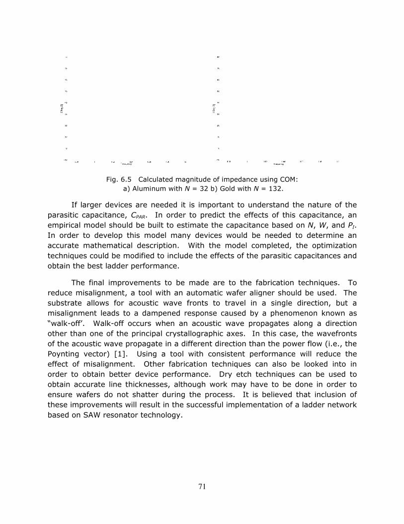
Fig. 6.5 Calculated magnitude of impedance using COM: a) Aluminum
If larger devices are needed it is important to understand the nature of the parasitic capacitance, CPAR. In order to predict the effects of this capacitance, an empirical model should be built to estimate the capacitance based on In order to develop this model many devices would be needed to determine an accurate mathematical description. Wtechniques could be modified to include the effects of the parasitic capacitances and obtain the best ladder performance.
The final improvements to be made are to the fabrication techniques. To reduce misalignment, a tool with an automatic wafer aligner should be used. The substrate allows for acoustic wave fronts to travel in a single direction, but a misalignment leads to a dampened response caused by a phenomenon known as “walk-off’. Walk-off occurs when an aother than one of the principal crystallographic axes. In this case, the wavefronts of the acoustic wave propagate in a different direction than the power flow (i.e., the Poynting vector) [1]. Using a tool with ceffect of misalignment. Other fabrication techniques can also be looked into in order to obtain better device performance. Dry etch techniques can be used to obtain accurate line thicknesses, although work mensure wafers do not shatter during the process. It is believed that inclusion of these improvements will result in the successful implementation of a ladder network based on SAW resonator technology.
71
Calculated magnitude of impedance using COM: a) Aluminum with N = 32 b) Gold with N = 132.
If larger devices are needed it is important to understand the nature of the . In order to predict the effects of this capacitance, an
empirical model should be built to estimate the capacitance based on In order to develop this model many devices would be needed to determine an accurate mathematical description. With the model completed, the optimization techniques could be modified to include the effects of the parasitic capacitances and obtain the best ladder performance.
The final improvements to be made are to the fabrication techniques. To t, a tool with an automatic wafer aligner should be used. The
substrate allows for acoustic wave fronts to travel in a single direction, but a misalignment leads to a dampened response caused by a phenomenon known as
off occurs when an acoustic wave propagates along a direction other than one of the principal crystallographic axes. In this case, the wavefronts of the acoustic wave propagate in a different direction than the power flow (i.e., the Poynting vector) [1]. Using a tool with consistent performance will reduce the effect of misalignment. Other fabrication techniques can also be looked into in order to obtain better device performance. Dry etch techniques can be used to obtain accurate line thicknesses, although work may have to be done in order to nsure wafers do not shatter during the process. It is believed that inclusion of these improvements will result in the successful implementation of a ladder network based on SAW resonator technology.
If larger devices are needed it is important to understand the nature of the . In order to predict the effects of this capacitance, an
empirical model should be built to estimate the capacitance based on N, W, and PI. In order to develop this model many devices would be needed to determine an
ith the model completed, the optimization techniques could be modified to include the effects of the parasitic capacitances and
The final improvements to be made are to the fabrication techniques. To t, a tool with an automatic wafer aligner should be used. The
substrate allows for acoustic wave fronts to travel in a single direction, but a misalignment leads to a dampened response caused by a phenomenon known as
coustic wave propagates along a direction other than one of the principal crystallographic axes. In this case, the wavefronts of the acoustic wave propagate in a different direction than the power flow (i.e., the
onsistent performance will reduce the effect of misalignment. Other fabrication techniques can also be looked into in order to obtain better device performance. Dry etch techniques can be used to
o be done in order to nsure wafers do not shatter during the process. It is believed that inclusion of these improvements will result in the successful implementation of a ladder network

72
References
[1] Velimir M. Ristic, Principles of Acoustic Devices. Toronto, Canada: John Wiley & Sons, 1983.
[2] R. M. White and F. W. Voltmer, “Direct piezoelectric coupling to surface elastic waves,” Appl. Phys. Lett.,vol. 7, pp. 314-315, Dec. 1965.
[3] R. M. White, “Surface elastic waves,” Proc. IEEE, vol. 58, pp.1238-1276, Aug. 1970.
[4] W. P. Mason, Physical Acoustics, vol. IA, Academic Press 1964 [5] L.A. Coldren and R. L. Rosenberg, "Surface-acoustic-wave resonator filters,"
Proceedings of the IEEE, vol. 67, no. 1, pp. 147-158, January 1979. [6] D. P. Morgan, Surface-Wave Devices for Signal Processing, Elsevier,
Amsterdam, 1985. [7] J. M. Deacon, J. Heighway, ”SAW Filters for TV Recievers,”
IEEE Trans. on Consumer Elec vol. CE-2, pp 390 -395, November 1975. [8] K. R. Lake, E. Cohen, T. L. Szabo, and J. A. Pustaver,
IEEE Trans. Circuits Syst., CAS-25, 241 (1978). [9] M. Yamaguchi, K. Y. Hashimoto, and H. Kogo, IEEE Trans. Son. Ultrason.,
SU-26, 53 (1979). [10] Haktmann, C. S., Wright, P. B., Kansy, R. J., and Garber, E. M.:
“Analysis of SAW IDT’s with internal reflections and the application of the design to single-phase unidirectional transducers” IEEE Ultrasonics Symposium Proc., pp. W 5, 1982.
[11] Lewis, M. F.: “SAW filters employing interdigitated interdigital transducers”, ibid., pp. 12-17
[12] E. K. Sittig and G. A Coquin, IEEE Trans. Son. Ultrason., SU-15, 111 (1968). [13] E. J. Staples, J. S. Schoenwald, R.C. Rosenfeld, and C.S. Hartmann, Proc.
IEEE Ultranson. Symp., 245 (1974). [14] 0. Ikata, T.Miyashita, T. Matsuda, T. Nishihara, and Y. Satoh,”Development
of low - loss band-pass filters using SAW resonators for portable telephones”, IEEE Ultraso. Symp. Proc., pp. 111 - 115, 1992.
[15] M. S. Dempsey, VHF-UHF Passive Filter Synthesis Based on Acoustic
Resonator Structures, RIT, Rochester, 2009. [16] S. Datta, Surface Acoustic Wave Devices, Prentice-Hall, Englewood Cliffs,
1986. [17] K. Hashimoto, T. Omori, and M. Yamaguchi, “Design Considerations on
Surface Acoustic Wave Resonators with Significant Internal Reflection in Interdigital Transducers”, IEEE Trans. Ultraso., pp 1394-1403, 2004.
[18] M. V. Klein, Optics, John Wiley & Sons, New York, 1970. [19] K. Hashimoto, Surface Acoustic Wave Devices in Telecommunications
Modelling and Simulation, Springer-Verlag, Berlin Heidelberg, 2000.

73
A Appendix
A.1 Hashimoto Code
%%%%%%%%%%%%%%%%%%%% %% Sean Dunphy RIT ADIML %% %% COM Theory %% %% March 4, 2010 %% %%%%%%%%%%%%%%%%%%%% clear; %% Design Parameters points = 1001; fn = linspace(0.9675,1.1057,points); PI = 18e-6; h = 1250e-10; W = 1981e-6; NI = 124; Nm = 400; PmPI = 16/18; Lg = 0; L = NI.*PI; %% Material Properties % Lithium Niobate 128 vo = 3985; % free velocity vm = 3884.11; % metalized velocity dvo = 111.888; % delta velocity Cs = 5.0e-10; % E0 + EPT - Material Property K2 = 0.056; % 2*((vo-vm)/vo) the coupling effeciency yo = 0.21e-3; % material parameter relating K2 to Cs units of mhos cx = 0.1e-10; % m/volt cy = 2.0e-10; % m/volt cz = 1.8e-10*1i; % m/volt % Aluminum p = 2695; ax = 2.5e10; az = 7.8e10; pv = p*(vo^2);

74
%% Velocity and Reflectivity %%%%%% Fv Fva = abs(cx)^2*(ax-pv); Fvb = abs(cy)^2*(pv); Fvc = abs(cz)^2*(az-pv); Fv = (K2/(2*Cs))*(Fva-Fvb+Fvc); %%%% Fz Fz = ((-pi*K2)/(Cs))*(((cx^2)*(ax+pv))+((cy^2)*pv)+((cz^2)*(az+pv))); % eq(6.10b) DATTA %%%% %%% %%%% Pz fig 6.8 in datta Pv = -1.48; %[email protected] [email protected] [email protected] Pz = -0.75; %[email protected] [email protected] [email protected] %%% % vshift = ((Pv*(K2/2))+(Fv*(h/PI)))*0.5; v = (vshift*vo)+vo; wc = 2*pi*(v/PI); f0 = wc/(2*pi); %%% r r = 1i.*((Pz.*((K2)./2))+(Fz.*(h./PI))).*sin(0.5.*pi.*fn); % reflectance per electrode %% Hashimoto Parameters k12 = (abs(r).*2)./PI; kp = k12.*PI; C = (Cs*W)/PI; chai = 2; alpha1 = (4*Cs*W*K2)/(pi()*chai*(PI^2)); z = sqrt(alpha1.*(2.*pi().*f0.*fn)); E0 = (z.*PI)./((2.*pi().*(fn-1))+kp); phi = sqrt((((2.*pi()).*(fn-1)).^2)-(kp.^2)); del = phi-(2.*pi().*(fn-1)); kpm = PmPI.*kp; phim = sqrt((((2.*pi()).*((fn.*PmPI)-1)).^2)-(kpm.^2)); delm = phim-(2.*pi().*((fn.*PmPI)-1)); %% P Matrix Coeffecients

75
p11 = (kp.*del.*(1-exp(-2.*1i.*NI.*phi)))./((kp.^2)-(del.^2).*exp(-2.*1i.*NI.*phi)); p12 = (exp(-1i.*NI.*phi).*((kp.^2)-(del.^2)))./((kp.^2)-(del.^2).*exp(-2.*1i.*NI.*phi)); p13 = E0.*(kp+del).*((1-exp(-1i.*NI.*phi))./(kp+del.*exp(-1i.*NI.*phi))); p33 = -2.*1i.*chai.*z.*E0.*L.*(1-((p33a.*(kp+del))./(kp.*exp(1i.*NI.*phi./2)+del.*exp(-1i.*NI.*phi./2))))+1i.*(2.*pi().*f0.*fn).*(C.*L+0e-12); %% Y One Port Resonator gammar = (kpm.*delm.*(1-exp(-2.*1i.*Nm.*phim)))./((kpm.^2)-(delm.^2).*exp(-2.*1i.*Nm.*phim)); gamma = gammar.*exp(-2.*1i.*2.*pi().*fn.*f0./v.*Lg); phiplus = angle(p12+p11); phigam = -1i.*log(gamma); phiI = atan2(imag(p33),real(p33)); Y = 1i.*abs(p33).*(sin(((phiplus+phigam)./2)+phiI)./sin((phiplus+phigam)./2)); Zpmatrix=1./Y;

76
A.2 Modification of Optimization Code
The optimization of ladder networks based on SAW resonator technology is done with the Cadence software suite. It has been shown that the Optimizer in the Analog Environment is capable of varying the SAW resonator parameters and producing a BVD circuit [15]. The work done in this thesis does not follow exactly the same steps. The target goal was not introduced as a circuit; a .csv file is generated by the filter function of interest, and loaded into Cadence using the ‘table’ function. The target function was to be met within 0.5% using the maximum number of iterations. When running a simulation with the maximum iterations, the option to graph each one should be turned off, as it will significantly decrease the simulation time. The simulations are also completed using the hybrid model, having a complex expression for Rm. In order for the simulation to work properly the real and imaginary parts must be evaluated separately to calculate the magnitude. This must be done because SKILL, the simulation language used by Cadence, is not able to process imaginary terms.
The frequency range used for simulation can give undesired results if not properly set up. The total frequency range simulated was at least twice that of the desired bandwidth. The frequency range was also centered on the target’s center frequency. If the frequency range is too narrow, or askew, the Optimizer will yield a flat line transfer function. The Optimizer must have proper boundaries for the input variables. For the simulations done PI was fixed to 17.6 µm and 18 µm for the series and parallel devices, respectively. The parameter N, the only parameter to be varied, had a lower bound of N = 10 and an upper bound of N = 800. The lower bound is set because previous work showed little response with N less than 10. The upper bound was set because any devices larger were unreasonable to fabricate. The factor f2, which relates W to N, was set to 7, for the simulations used to design the OptimatorF mask. This number was based on the devices from the OptimatorM mask that showed the most desirable results.

77
A.3 RF Measurement and Calibration Techniques
The S parameters of the SAW devices were measured using the Agilent Technologies E5071C Network Analyzer. This appendix will detail how to measure and convert the S parameters of the SAW resonator device. The S matrix is written as,
0§WW §W§W §4 . ¨. 3.1 Each parameter describes a different cause and effect relationship at each of the ports. S11 is the reflected portion of the incident wave on the DUT from port 1. S21 is the forward traveling wave at the second port due to the forward traveling wave at the first port. The SAW resonator device is bi-directional, meaning that the device behaves in the same manner from either direction. The following equalities can be made, S11 = S22, and S21 = S12. The test set up is shown below in Figure A.1.
Fig. A.1 Test setup for SAW resonator.
The network analyzer measures the DUT, in relation to the characteristic impedances, Z0, that terminate both ports of the device. The value of Z0 for these tests is 50 ohms. The voltages at each port can be described by the number of the port, as well as the direction the voltage is traveling. The ports ‘1’ and ‘2’ are represented in the subscripts, and directionality is represented in the superscripts by ‘-‘ and ‘+’. The superscript ‘-‘ indicates travelling back towards the source, and ‘+’ travelling away from the source. No superscript on the voltage term signifies

78
the summation of the forward and reverse waves at the respective port. The S parameters for the SAW resonator can be written as,
§WW kWAkWc ]©ª]©ª 2] ¨. 3.2 and
§W kckWc kkW 1 §WW ]]©ª 2] 1 ]©ª]©ª 2] ¨. 3.3 since V2- is zero. It is possible to rearrange these equations in order to solve for the impedance as,
]©ª 2]§WW1 . §WW 2]1 . §W§W . ¨. 3.4 This allows the measured results to be converted into impedance which can be compared to the theoretical development. To convert the S parameter measurements to the impedance of the resonator, the S11 measurement was used in preference to the S21. The reason for this is that the spectral response of S21 typically does not show large changes in value, and is therefore susceptible to measurement uncertainty. When measuring full ladder networks the S21 measurement was used because it is closely related to the transfer function, H. This relationship is,
« kkW kc kAkWc kWA kckWc1 §WW §W1 §WW , ¨. 3.5 where V2- equals zero for the test set up in Figure A.2.
Fig. A.2 Test setup for SAW resonator based ladder network.
In order to obtain the measurement, accurate calibration of the tool must be completed. The full-two port calibration includes an open, a short, a load, and a through. All of these measurements can be made on either a calibration standard, or calibration test structures, with the exception of the load measurement. It isn't

79
reasonable to fabricate four identical 100 ohm resistors from a one metal layer process. By calibrating the probes on the substrate it is possible to eliminate the resistance caused by the metal traces. When this is done other effects are introduced to the measurement, which dominate phase measurements and cannot be accounted for. Using the off-chip calibration includes the series resistance, but any parasitic features can be measured and accounted for. During the two-port calibration the S11 and S22 measurements can be read independently in order to ensure matching behavior.
The network analyzer has many settings which should be given appropriate values in order to obtain clear results. The frequency span should be set to include the operation of all devices to be measured, for testing 210 MHz to 240 MHz was used. The number of points between these two frequencies was 1001, and the tool swept the frequency to go between each point. It is also possible to step the frequency discretely; doing this will add noise to the measurement. Slow changes to frequency also improve measurement clarity; the analyzer was set to take measurements over 15 seconds. These settings provided measurements with the least noise in a reasonable amount of time.
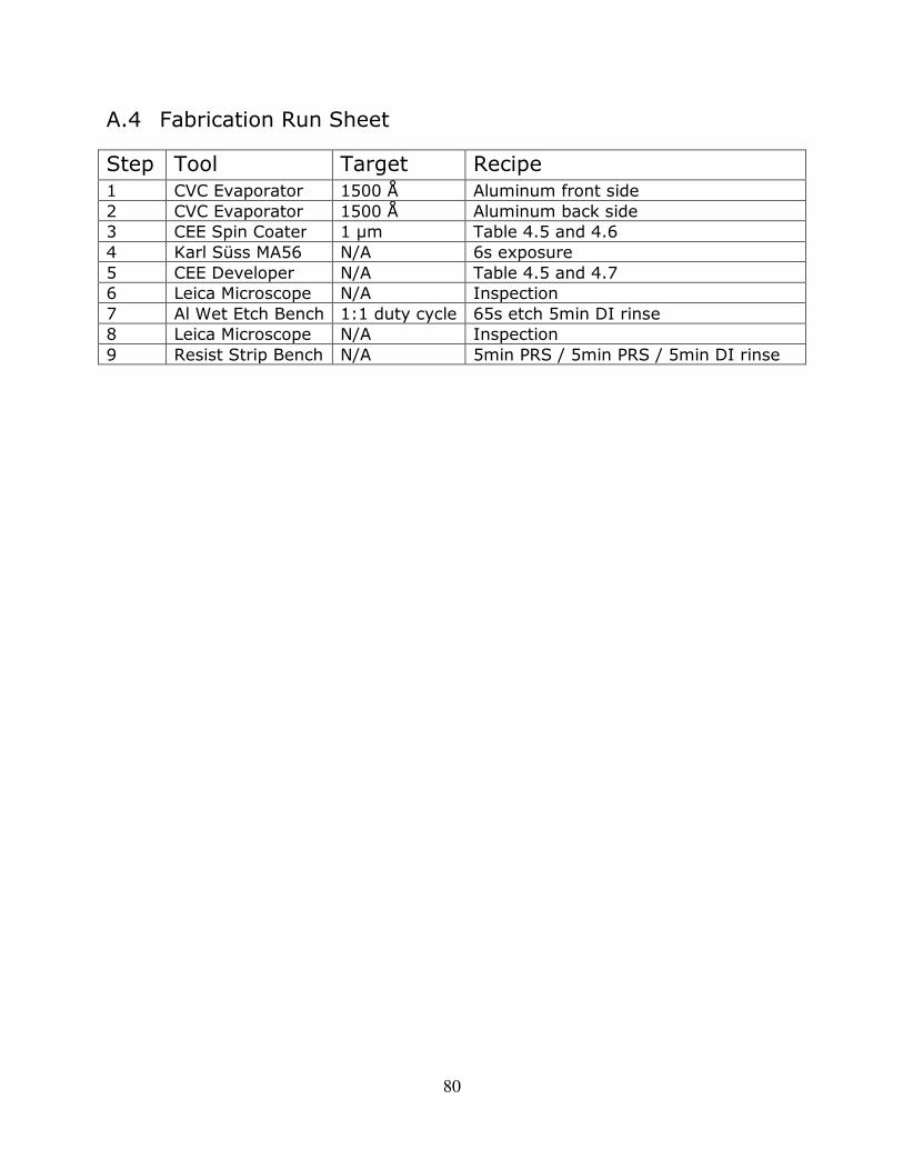
80
A.4 Fabrication Run Sheet
Step Tool Target Recipe 1 CVC Evaporator 1500 Å Aluminum front side 2 CVC Evaporator 1500 Å Aluminum back side 3 CEE Spin Coater 1 µm Table 4.5 and 4.6 4 Karl Süss MA56 N/A 6s exposure 5 CEE Developer N/A Table 4.5 and 4.7 6 Leica Microscope N/A Inspection 7 Al Wet Etch Bench 1:1 duty cycle 65s etch 5min DI rinse 8 Leica Microscope N/A Inspection 9 Resist Strip Bench N/A 5min PRS / 5min PRS / 5min DI rinse