design and implementation of an electro-optical backplane...
TRANSCRIPT
Design and implementation of an electro-optical backplane with
pluggable in-plane connectors
Richard C. A. Pitwon*a, Ken Hopkins
a, Kai Wang
b, David R. Selviah
b, Hadi Bagshiahi
b, Bert J.
Offreinc, Roger Dangel
c, Folkert Horst
c, Markus Halter
d, Max Gmür
d
aXyratex Technology Ltd, 1000-40 Langstone Technology Park, Havant, Hampshire, PO9 1SA, UK;
bElectronic and Electrical Engineering, University College London, Torrington Place, London;
WC1E 7JE, UK; cIBM Research GmbH, IBM Research - Zurich, Säumerstrasse 4, 8803, Rüschlikon, Switzerland;
dVarioprint AG , Mittelbissaustrasse 9, CH-9410 Heiden, Switzerland
ABSTRACT
The design, implementation and characterisation of an electro-optical backplane and an active pluggable
optical connector technology are presented. The connection architecture adopted allows line cards to mate
and unmate from a passive electro-optical backplane with embedded polymeric waveguides. The active
connectors incorporate photonics interfaces operating at 850 nm and a mechanism to passively align the
interface to the embedded optical waveguides. A demonstration platform has been constructed to assess the
viability of embedded electro-optical backplane technology in dense data storage systems. The electro-optical
backplane is comprised of both copper layers and one polymeric optical layer, whereon waveguides have
been patterned by a direct laser writing scheme. The optical waveguide design includes arrayed multimode
waveguides with a pitch of 250 μm, multiple cascaded waveguide bends, non-orthogonal crossovers and in-
plane connector interfaces. In addition, a novel passive alignment method has been employed to simplify high
precision assembly of the optical receptacles on the backplane. The in-plane connector interface is based on a
two lens free space coupling solution, which reduces susceptibility to contamination. The loss profiles of the
complex optical waveguide layout has been characterised and successful transfer of 10.3 Gb/s data along
multiple waveguides in the electro-optical backplane demonstrated. Keywords: optical printed circuit boards, optical interconnect, waveguides, polymer, optical alignment, pluggable
optical connector
1. INTRODUCTION
Emerging trends in the data storage industry are poised to severely impact the design of future data storage systems. The
last decade has seen a dramatic increase in the volume of data being captured, processed, stored and manipulated as
digital information. This information is generated from many sources, including critical business applications, email
communications, the Internet and multimedia applications which have collectively fuelled an increase in demand for
data storage capacity. However the increase in system bandwidth and density required to satisfy this demand would
impose unmanageable cost and performance burdens on future data storage array technologies. In particular, the
reduction in size of peripheral storage devices - such as hard disk drives – will cause the density of printed channels on
the data storage backplane to go up, while the increase in data communication speeds will expose the system to some of
the fundamental constraints incurred when higher frequency data is conveyed along electronic channels. Many of these
constraints, which include crosstalk, dielectric loss, skin effect and electro-magnetic interference, can be mitigated to
some degree, however at a mounting cost to the overall system design.
*[email protected]; phone : +44 (0)23 9249 6715; fax +44 (0)23 9249 2284; website: www.xyratex.com

It is proposed that the resulting performance bottleneck be substantially reduced by conveying high speed data optically
instead of electronically. This requires that optical channels be incorporated into the system at the printed circuit board
(PCB) level. While significant advances have been made in Japan1 in embedding conventional optical fibres onto printed
circuit boards, focus across Europe and North America over the past decade has been on the fabrication of transparent
plastic channels (waveguides) directly onto the printed circuit board substrates. Berger2, Dangel
3, Van Steenberge
3,
Chappell4 , Shibata
5 and Doany
7 have collectively demonstrated a wide range of waveguide fabrication techniques,
however a number of challenges remain to be solved before this technology can reach its full commercial potential.
One crucial requirement is a reliable method of connecting peripheral devices to an optical printed circuit board in a
pluggable manner. Recent advances in this field8 have shown how fibre-optic cables can be connected orthogonally to
optical channels embedded in the circuit board. This approach however requires that right-angled mirrors be
incorporated, which can be costly and difficult to implement on a commercial scale. To overcome this issue, we have
developed a method of connecting to an optical printed circuit board, which not only precludes the need for embedded
mirrors, but also intermediary fibre-optic cables. Xyratex has generated a broad patent portfolio in the field of optical
printed circuit boards including passive and active optical connectors, precision alignment and assembly techniques,
optical PCB fabrication and novel embedded waveguide structures.
In this paper we consider the design challenges inherent to a modern data storage system and the technologies required
to implement an embedded optical architecture. To evaluate the viability of these technologies, we have developed and
successfully demonstrated an electro-optical backplane connection system. We describe and characterise the key
elements of the system including pluggable active optical connectors, a passive alignment and assembly method, the
electro-optical backplane and the complex optical interconnect pattern fabricated thereon. Parallel optical data streams
with a modulation rate of 10.3 Gb/s have been successfully conveyed across the backplane between all peripheral
devices.
Figure 1: Modern data storage array with hard disk drives connected to one side of the backplane (or midplane)
and controller boards and power supplies connected to the other

2. DESIGN CHALLENGES IN MODERN DATA STORAGE ARCHITECTURES
In a typical data storage system (see Figure 1), an array of hard disk drives are connected to one side of a passive
backplane (or midplane) while controller modules (or storage bridge bays) and power supplies are connected to the other
side. As shown, the backplane and its peripherals are connected in a mutually orthogonal geometry.
2.1 Data storage backplane topology
Due to the critical redundancy requirements in modern data storage systems, the interconnect topology essentially
describes a dual star configuration, whereby each disk drive conveys a duplex data link across the backplane to each of
two separate controller modules. Each duplex link in turn comprises a pair of transmission lines. A number of additional
duplex links directly connect the controller modules to each other. The Storage Bridge Bay Specification9 allows for a
maximum of 48 disk drives in an enclosure, each supporting two duplex links, with a further 17 duplex links between
controller modules. The backplane of a 48 drive storage array would therefore have to accommodate 113 duplex links or
226 high speed transmission lines. The level of fault tolerance and scalability offered by these topologies is significant,
however this forces increased complexity and cost into the backplane, particularly when interconnect protocols define
serial data rates beyond 10 Gb/s.
2.2 Interconnect protocols in the data storage domain
Serial Attached SCSI (SAS) is the dominant protocol governing the interconnect on data storage backplanes and
therefore the maximum speed with which data is conveyed to and from the storage system peripherals (hard drives,
controller modules). The SAS roadmap10
currently defines a serial data rate of 6 Gb/s, which is projected to double to 12
Gb/s by 2012/2013 with the next protocol iteration, while the Fibre Channel protocol, which governs host connectivity in
the wider storage network is expected to increase from 8 Gb/s today to 16 Gb/s by 201111
.
2.3 Design and performance constraints
There are a number of factors, which will limit the operational bit rate of the high speed links on a commercial copper
backplane. Dielectric absorption and Skin Effect are the key loss mechanisms on a copper trace, which cause an increase
in signal attenuation with frequency, while electro-mechanical connectors introduce parasitic capacitance and inductance
effects and vias can act as impedance stubs giving rise to partial reflections in the signal path. At signal data rates of 12
Gb/s, additional design measures will be imperative including the use of PCB substrates with lower dielectric loss
tangents, electro-mechanical connectors, which impart lower skew on differential traces and enhanced via control
techniques such as backdrilling. In order to mitigate rising crosstalk, copper channels will need to be moved further
apart, however due to the areal constraints of the enclosure form factor more complex routing patterns will be required
and the number of high speed layers in the backplane PCB increased. The available space on the backplane is further
restricted by the need for milled access slots to allow sufficient air flow through the system.
Our ultimate aim will be to embed optical channels into the data storage backplane in order to overcome the critical
communications bottleneck thereon and develop technologies enabling the peripheral devices to optically plug to and
unplug from the backplane.
3. ELECTRO-OPTICAL BACKPLANE WITH POLYMERIC WAVEGUIDES
A passive electro-optical backplane was designed, which includes electrical layers devoted power distribution and low-
speed bus communication and one polymeric optical interconnect layer to convey high speed serial data between
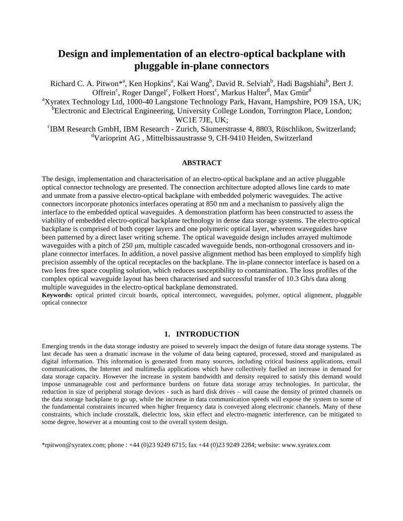
peripheral connectors (see Figure 2).
Figure 2: An electro-optical backplane and a waveguide illuminated with 635 nm light exiting one of the
connector slots
3.1 Polymer optical waveguide layer
An optical interconnect layer was fabricated on the outer surface of the backplane PCB from a proprietary polymer
exhibiting low optical absorption at a wavelength of 850 nm. The optical layer comprised a core, sandwiched between a
lower and an upper cladding, whereby the polymer in the core layer had a slightly higher refractive index than that in the
bounding cladding layers. Rectangular channels were patterned in the core layer with a cross-section of 70 μm x 70 μm
defining waveguides of a size suitable to meet the launch and capture tolerances on the optical transmit and receive
elements. The refractive index of the core material ncore = 1.56, while that of the cladding ncladding = 1.524, giving rise to
step-index multimode waveguides with a core - cladding index difference of ∆n = 2.3% and a numerical aperture (N.A.)
of 0.33.
3.2 Optical interconnect design
The optical interconnect layer, designed by UCL, Xyratex and IBM Zurich was framed by a complex routing pattern
(Figure 3), which included four quasi-rectangular optical engagement apertures, non-orthogonal crossovers and
cascading bends. It was deemed important that the optical layout reflect the routing constraints that would be typically
encountered in a real backplane design. The sizes of the engagement apertures were determined by the pluggable
connector prototype, which will be described in the next section. The engagement apertures are interconnected by a
point-to-point waveguide network, whereby each aperture maintains one bidirectional link (comprising two waveguides)
to every other aperture, resulting in a total of 12 waveguides on the board. All waveguides, but two, have four cascaded
90º bends comprising a negative cascade followed by a positive cascade. A negative cascade occurs when one 90º bend
is followed by another 90º bend, which curves in the opposite direction to the first bend, giving rise to an inflection point
in the waveguide and a net waveguide angle change of 0º. A positive cascade occurs when one 90º bend is followed by
another 90º bend, curving in the same direction as the first and thus giving rise to a net waveguide angle change of 180º.
The decomposition of waveguides into right-angled bend segments in this fashion can be an aid to optical simulation. To
minimise bend losses, a radius of curvature of 17mm was applied on all bends as this was the maximum permitted by the
routing constraints on the board. A number of waveguides intersect in one or more positions along the waveguide. To
accommodate space restrictions the crossing angles chosen range from 130º to 160º, which equate to a deviation from
the optimum perpendicular crossing angle of 40º to 70º. Though the relatively large minimum bend radii required at this
stage would place significant routing constraints on future optical printed circuit board layouts, these could be effectively
mitigated by refinement of manufacturing techniques, further flexibility in crossing angles and in particular adoption of
in-plane mirrored bends12
.

Figure 3: Optical waveguide layout including cascaded bends and non-orthogonal crossovers
3.3 Electro-optical PCB fabrication process
The electro-optical backplane fabricated by Varioprint and IBM Zurich was built up of 10 copper layers and one
polymeric layer. Preliminary lamination tests on the electrical layers showed significant thickness tolerances on the
complete stack-up of the PCB. If the optical layer were to have been deposited directly onto the electrical PCB, these
would have given rise to unacceptably large variations in waveguide height of ±18μm. To overcome this issue, it was
decided that the optical layer be fabricated on a separate flexible substrate, which would later be laminated to the
electrical PCB.
A proprietary liquid cladding polymer was deposited onto a polyimide substrate with a doctor-blading process applied to
control the thickness. The photosensitive polymer was uniformly cured with ultraviolet light to form the lower cladding
layer. A higher index liquid core polymer was then deposited onto the lower cladding layer and doctor-bladed to a
thickness of 70 μm. The core features were patterned using a vectorial Laser Direct Imaging technique whereby an
(a) (b)
Figure 4: (a) Clearance areas in upper cladding layer to provide mechanical access for optical connector
receptacle and waveguide end facet
(b) An exposed waveguide structure serves as a passive alignment feature for the assembly of the optical
connector receptacle

ultraviolet laser was moved across the substrate to selectively cure those parts of the core layer which would form the
waveguides. The upper cladding was deposited in a similar fashion to the lower cladding, however instead of a uniform
cure, certain areas of the upper cladding were masked in order to provide mechanical access to registration features in
the core layer as shown in Figures 4 (a) and (b). These registration features in turn allow passive assembly of the optical
connector receptacle to the PCB according to a proprietary self-alignment technique13
. Mechanical slots were milled into
the polyimide backed optical layer and compliant pins assembled onto the electrical PCB in order to align both
substrates together prior to a cold lamination process. Finally the optical engagement apertures were milled out along
with the outline of the backplane, which was 262 mm long, 240 mm high and 4 mm thick.
3.4 Insertion loss measurements
The design of the optical interconnect was guided by prior research14, 15
into photolithographically fabricated waveguides
comprised of Truemode® polymer16
. The measurements conducted by UCL and Xyratex, provided a framework to
extrapolate the attenuation on a waveguide exhibiting a variety of geometric characteristics including bends, crossings
and interfaces. The waveguides in the optical interconnect layout were designed to exhibit an insertion loss of less than
12 dB. The following experimental setup was used to measure the insertion loss on 9 waveguides on the electro-optical
backplane. A 10 metre length of step-index multimode optical fibre with a 50 μm core and N.A.fibre = 0.2, was connected
to an 850 nm VCSEL source on one end, while the other end was aligned and butt-coupled to the waveguide core with a
larger N.A.waveguide = 0.33. A number of 15 cm diameter winds in the fibre provided sufficient inter-mode coupling to
ensure a uniform modal distribution pattern at the launch point into the waveguide. The optical power at the launch point
was measured to be 0.00 ±0.10 dBm. A silicon photodetector with an 8 mm aperture was aligned to the output of the
waveguide to measure insertion loss, which included coupling losses at the fibre-waveguide interface, absorption by the
propagation medium, transition losses due to modal mismatch between bend segments and losses incurred at crossing
junctions. The launch fibre was mounted on a motorised translation stage with sub-micron step resolution, which was
controlled to optimise light capture by the waveguide core. An index matching fluid (n = 1.5694 ± 0.0005 at 589.3 nm)
was also applied to the fibre-waveguide and waveguide-photodetector interfaces to reduce surface scattering and Fresnel
back-reflections. Insertion loss measurements were made on 9 waveguides both with and without index matching fluid
applied.
The measurement results are shown in Figure 5 along with the original calculated values and highlight the strong
dependence of loss on end facet roughness.
Figure 5: Projected and measured values for insertion loss on a group of 9 waveguides
Insert
ion
Lo
ss p
er
Waveg
uid
e (
dB
)
Waveguides sorted by total length
4. ACTIVE OPTICAL BACKPLANE CONNECTOR
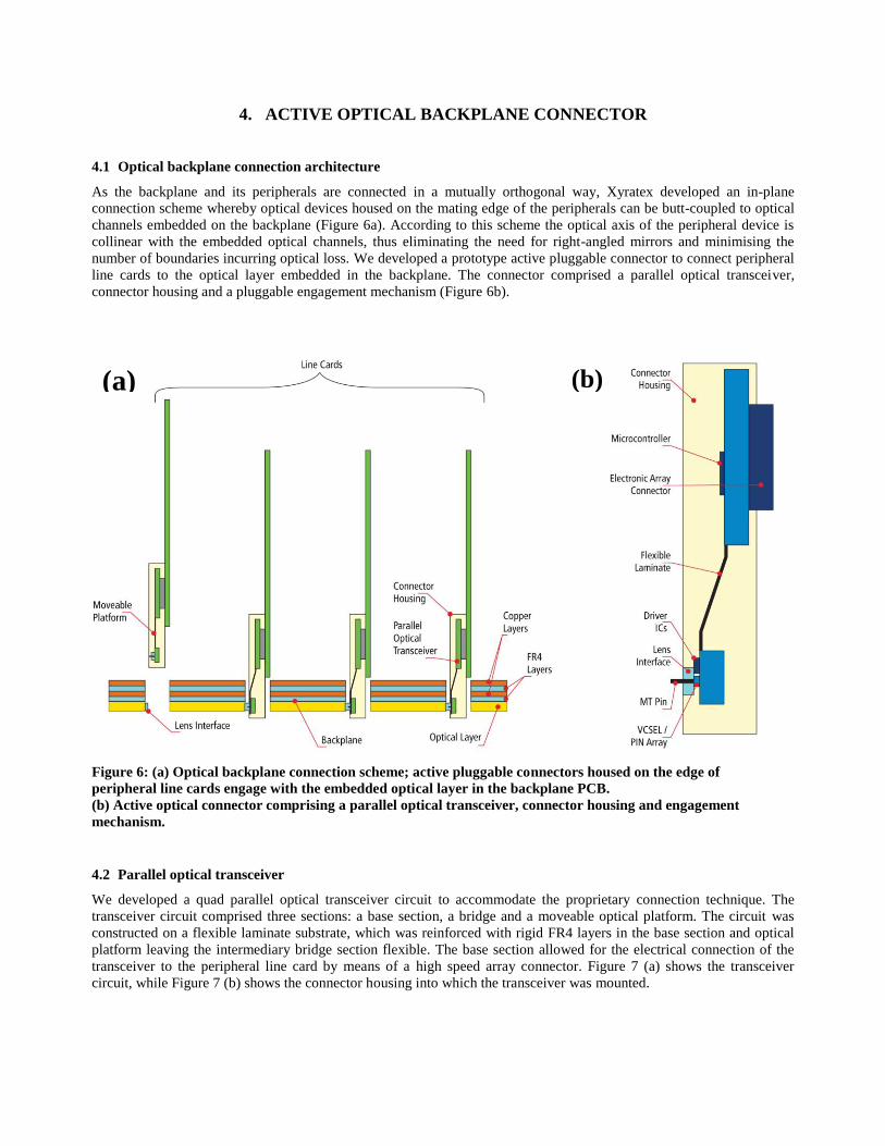
4.1 Optical backplane connection architecture
As the backplane and its peripherals are connected in a mutually orthogonal way, Xyratex developed an in-plane
connection scheme whereby optical devices housed on the mating edge of the peripherals can be butt-coupled to optical
channels embedded on the backplane (Figure 6a). According to this scheme the optical axis of the peripheral device is
collinear with the embedded optical channels, thus eliminating the need for right-angled mirrors and minimising the
number of boundaries incurring optical loss. We developed a prototype active pluggable connector to connect peripheral
line cards to the optical layer embedded in the backplane. The connector comprised a parallel optical transceiver,
connector housing and a pluggable engagement mechanism (Figure 6b).
4.2 Parallel optical transceiver
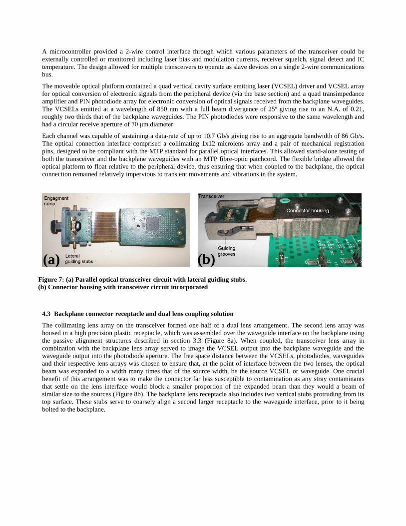
We developed a quad parallel optical transceiver circuit to accommodate the proprietary connection technique. The
transceiver circuit comprised three sections: a base section, a bridge and a moveable optical platform. The circuit was
constructed on a flexible laminate substrate, which was reinforced with rigid FR4 layers in the base section and optical
platform leaving the intermediary bridge section flexible. The base section allowed for the electrical connection of the
transceiver to the peripheral line card by means of a high speed array connector. Figure 7 (a) shows the transceiver
circuit, while Figure 7 (b) shows the connector housing into which the transceiver was mounted.
(a) (b)
Figure 6: (a) Optical backplane connection scheme; active pluggable connectors housed on the edge of
peripheral line cards engage with the embedded optical layer in the backplane PCB.
(b) Active optical connector comprising a parallel optical transceiver, connector housing and engagement
mechanism.
A microcontroller provided a 2-wire control interface through which various parameters of the transceiver could be
externally controlled or monitored including laser bias and modulation currents, receiver squelch, signal detect and IC
temperature. The design allowed for multiple transceivers to operate as slave devices on a single 2-wire communications
bus.
The moveable optical platform contained a quad vertical cavity surface emitting laser (VCSEL) driver and VCSEL array
for optical conversion of electronic signals from the peripheral device (via the base section) and a quad transimpedance
amplifier and PIN photodiode array for electronic conversion of optical signals received from the backplane waveguides.
The VCSELs emitted at a wavelength of 850 nm with a full beam divergence of 25º giving rise to an N.A. of 0.21,
roughly two thirds that of the backplane waveguides. The PIN photodiodes were responsive to the same wavelength and
had a circular receive aperture of 70 μm diameter.
Each channel was capable of sustaining a data-rate of up to 10.7 Gb/s giving rise to an aggregate bandwidth of 86 Gb/s.
The optical connection interface comprised a collimating 1x12 microlens array and a pair of mechanical registration
pins, designed to be compliant with the MTP standard for parallel optical interfaces. This allowed stand-alone testing of
both the transceiver and the backplane waveguides with an MTP fibre-optic patchcord. The flexible bridge allowed the
optical platform to float relative to the peripheral device, thus ensuring that when coupled to the backplane, the optical
connection remained relatively impervious to transient movements and vibrations in the system.
4.3 Backplane connector receptacle and dual lens coupling solution
The collimating lens array on the transceiver formed one half of a dual lens arrangement. The second lens array was
housed in a high precision plastic receptacle, which was assembled over the waveguide interface on the backplane using
the passive alignment structures described in section 3.3 (Figure 8a). When coupled, the transceiver lens array in
combination with the backplane lens array served to image the VCSEL output into the backplane waveguide and the
waveguide output into the photodiode aperture. The free space distance between the VCSELs, photodiodes, waveguides
and their respective lens arrays was chosen to ensure that, at the point of interface between the two lenses, the optical
beam was expanded to a width many times that of the source width, be the source VCSEL or waveguide. One crucial
benefit of this arrangement was to make the connector far less susceptible to contamination as any stray contaminants
that settle on the lens interface would block a smaller proportion of the expanded beam than they would a beam of
similar size to the sources (Figure 8b). The backplane lens receptacle also includes two vertical stubs protruding from its
top surface. These stubs serve to coarsely align a second larger receptacle to the waveguide interface, prior to it being
bolted to the backplane.
(a) (b)
Figure 7: (a) Parallel optical transceiver circuit with lateral guiding stubs.
(b) Connector housing with transceiver circuit incorporated
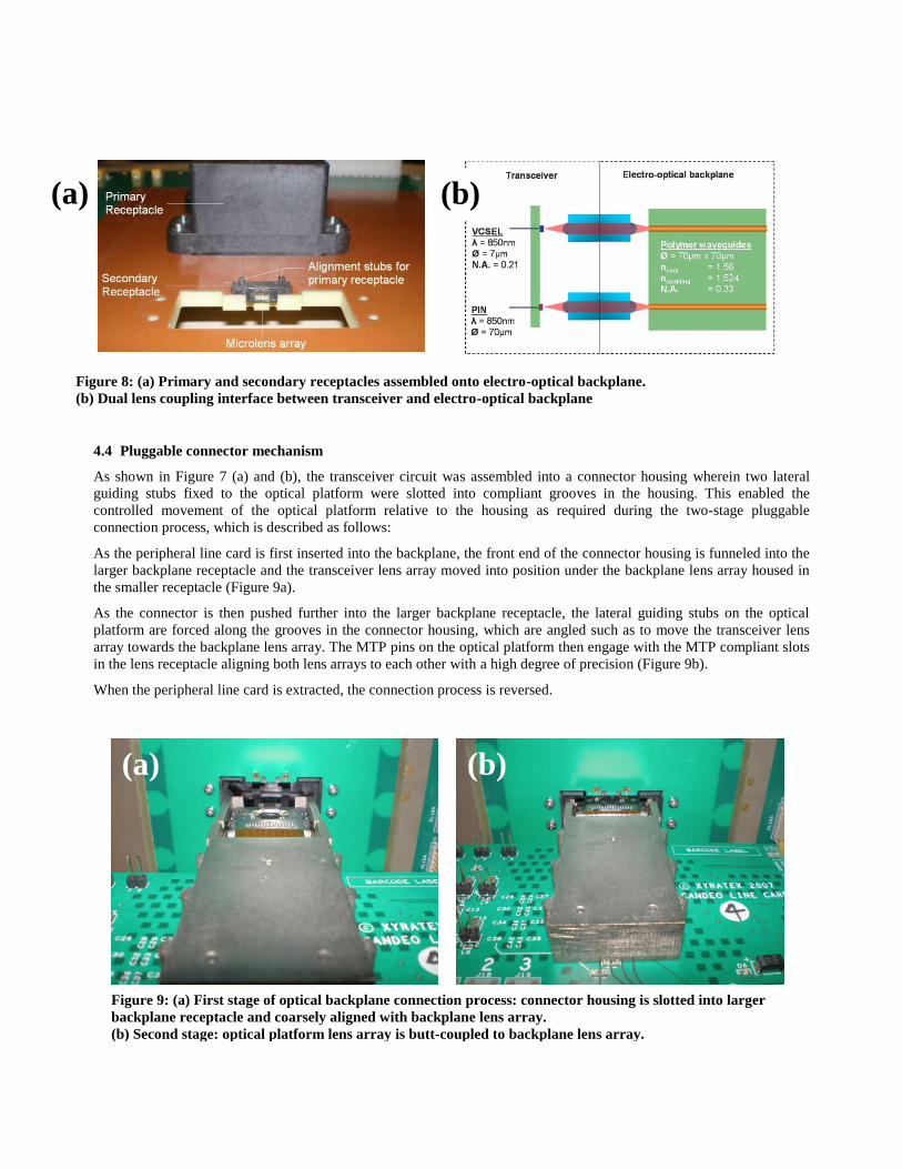
4.4 Pluggable connector mechanism
As shown in Figure 7 (a) and (b), the transceiver circuit was assembled into a connector housing wherein two lateral
guiding stubs fixed to the optical platform were slotted into compliant grooves in the housing. This enabled the
controlled movement of the optical platform relative to the housing as required during the two-stage pluggable
connection process, which is described as follows:
As the peripheral line card is first inserted into the backplane, the front end of the connector housing is funneled into the
larger backplane receptacle and the transceiver lens array moved into position under the backplane lens array housed in
the smaller receptacle (Figure 9a).
As the connector is then pushed further into the larger backplane receptacle, the lateral guiding stubs on the optical
platform are forced along the grooves in the connector housing, which are angled such as to move the transceiver lens
array towards the backplane lens array. The MTP pins on the optical platform then engage with the MTP compliant slots
in the lens receptacle aligning both lens arrays to each other with a high degree of precision (Figure 9b).
When the peripheral line card is extracted, the connection process is reversed.
(a) (b)
Figure 9: (a) First stage of optical backplane connection process: connector housing is slotted into larger
backplane receptacle and coarsely aligned with backplane lens array.
(b) Second stage: optical platform lens array is butt-coupled to backplane lens array.
(a) (b)
Figure 8: (a) Primary and secondary receptacles assembled onto electro-optical backplane.
(b) Dual lens coupling interface between transceiver and electro-optical backplane
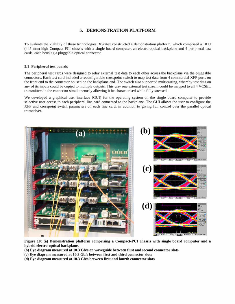
5. DEMONSTRATION PLATFORM
To evaluate the viability of these technologies, Xyratex constructed a demonstration platform, which comprised a 10 U
(445 mm) high Compact PCI chassis with a single board computer, an electro-optical backplane and 4 peripheral test
cards, each housing a pluggable optical connector.
5.1 Peripheral test boards
The peripheral test cards were designed to relay external test data to each other across the backplane via the pluggable
connectors. Each test card included a reconfigurable crosspoint switch to map test data from 4 commercial XFP ports on
the front end to the connector housed on the backplane end. The switch also supported multicasting, whereby test data on
any of its inputs could be copied to multiple outputs. This way one external test stream could be mapped to all 4 VCSEL
transmitters in the connector simultaneously allowing it be characterised while fully stressed.
We developed a graphical user interface (GUI) for the operating system on the single board computer to provide
selective user access to each peripheral line card connected to the backplane. The GUI allows the user to configure the
XFP and crosspoint switch parameters on each line card, in addition to giving full control over the parallel optical
transceiver.
Figure 10: (a) Demonstration platform comprising a Compact-PCI chassis with single board computer and a
hybrid electro-optical backplane.
(b) Eye diagram measured at 10.3 Gb/s on waveguide between first and second connector slots
(c) Eye diagram measured at 10.3 Gb/s between first and third connector slots
(d) Eye diagram measured at 10.3 Gb/s between first and fourth connector slots
(a) (b)
(c)
(d)

5.2 High speed data transmission measurement
An external 10 Gb Ethernet LAN traffic source was arranged to convey a 10.3 Gb/s test data stream along a fibre-optic
cable to one of the commercial XFP devices on the front end of a peripheral test card in the demonstration platform. The
XFP device converted the optical data stream to a serial electronic data stream on the test card, which was then mapped
by the crosspoint switch to one of the VCSEL transmitters in the connector attached to that card and reconverted into an
optical data stream. As the connector was optically engaged to the backplane, the optical data stream was launched into a
waveguide and conveyed to the receive element of another connector on a different test card in the chassis. The data was
then converted to a serial electronic data stream, mapped to an XFP port on that test card and reconverted to an optical
data stream on the output of the XFP device. Finally a fibre-optic cable connected the XFP output port to a
communications signal analyser where the test data was characterised.
In total 9 waveguides were tested as described and 10.3 Gb/s test data has been successfully conveyed between all test
cards and their prototype connectors with an acceptable level of signal recovery. Figures 10 (b), (c) and (d) show the eye
diagrams of 3 typical waveguides of different lengths. The peak to peak jitter was consistently measured to be around 26
ps.
6. CONCLUSIONS
The burgeoning demand for faster and more compact data storage systems is fuelling the need for embedded optical
interconnect solutions. To this end we have developed and successfully demonstrated an active optical interconnect
solution which will allow peripheral devices to plug into and unplug from an electro-optical backplane. Our results have
been promising and show that a complex optical interconnect pattern of polymer waveguides could be used to effectively
convey high speed optical data across a densely populated board with a rack size of at least 6U.
ACKNOWLEDGEMENTS
We would like to thank Samtec for their involvement with and contribution to this research initiative. We also gratefully
acknowledge our partners on the IeMRC OPCB project for their counsel and assistance, in particular Stevenage
Circuits, BAE Systems, Dow Corning, Cadence, NPL, Heriot Watt University and Loughborough University.
REFERENCES
[1] M. Ohmura and K. Saito, High-Density Optical Wiring Technologies for Optical Backplane Interconnection Using
Downsized Fibers and Pre-Installed Fiber Type Multi Optical Connectors, Optical Fiber Communication
Conference and Exposition and The National Fiber Optic Engineers Conference, Technical Digest (CD) (Optical
Society of America, 2006), paper OWI71.
[2] C. Berger, M. Kossel, C. Menolfi, T. Morf, T. Toifl, and M. Schmatz High-density optical interconnects within
large-scale systems, Proc. SPIE, vol. 4942, pp. 222-235 (2003)
[3] R. Dangel, C. Berger, R. Beyeler, L. Dellmann, M. Gmuer, R. Hamelin, F. Horst, T. Lamprecht, T. Morf, S.
Oggioni, M. Spreafico, B. J. Offrein, “Polymer Waveguide based board-level optical interconnect technology for
datacom applications,” IEEE Trans. Advanced Packaging, 31, pp. 759-767 (2008).
[4] G. Van Steenberge, P. Geerinck, S. Van Put, J. Van Koetsem, H. Ottevaere, D. Morlion, H. Thienpont, and P. Van
Daele, MT-compatible laser-ablated interconnections for optical printed circuit boards, J. Lightwave Technol. 22,
pp. 2083–2090 (2004)

[5] Selviah, D.R. Hutt, D.A. Walker, A.C. Wang, K. Fernandez, F.A. Conway, P.P. Milward, D.
Papakonstantinou, I. Baghsiahi, H. Chappell, J. Zakariyah, S.S. McCarthy, A. Suyal, H, Innovative Optical
and Electronic Interconnect Printed Circuit Board Manufacturing research, ESTC 2008, (2) pp. 867-872 (2008)
[6] Shibata, T. Takahashi, A, Flexible opto-electronic circuit board for in-device interconnection ECTC 2008 (58) pp.
261-267 (2008)
[7] F. E. Doany, C.L. Schow, C.W. Baks, D.M. Kuchta, P. Pepeljugoski, L. Schares, R. Budd, F. Libsch, R. Dangel, F.
Horst, B.J. Offrein, J.A. Kash, “160 Gb/s bidorectional polymer-waveguide board-level optical interconnects using
CMOS-based transceivers,” IEEE Trans. Advanced Packaging, 32, pp. 345-359 (2009).
[8] A. Glebov, M. Lee, and K. Yokouchi, “Integration technologies for pluggable backplane optical interconnect
systems,” J. Opt. Eng. 46, no. 1, pp. 015403-1–015403-10, Jan. 2007
[9] Storage Bridge Bay Working Group, Inc “Storage Bridge Bay Specification” Version 2.0. 2008
[10] http://www.scsita.org/aboutscsi/sas/SAS_roadmap.html - SCSI Trade Association “Serial Attached SCSI Roadmap“
September 2009
[11] Fibre Channel Industry Association “FCIA Official Roadmap” v11 20th
March 2009
[12] Dan A Zauner, Anders M Jorgensen, Thomas A Anhoj and Jorg Hubner “High-density multimode integrated
polymer optics” J. Opt. A: Pure Appl. Opt. 7 pp. 445-450 (2005)
[13] Papakonstantinou,I., Selviah,D.R., Pitwon,R.A., Milward,D. (2008). “Low cost, precision, self-alignment technique
for coupling laser and photodiode arrays to waveguide arrays,” IEEE Transactions on Advanced Packaging . ISSN:
1521-3323
[14] I. Papakonstantinou, K. Wang, D. R. Selviah, and F. A. Fernández, "Transition, radiation and propagation loss in
polymer multimode waveguide bends," Optics Express, vol. 15, no. 2, pp. 669-679, Jan.2007
[15] K. Wang, D. R. Selviah, I. Papakonstantinou, G. Yu, H. Baghsiahi, and F. A. Fernández, "Photolithographically
Manufactured Acrylate Multimode Optical Waveguide Loss Design Rules," 2nd Electronics System-Integration
Technolgy Conference (ESTC), Session Th-P-9, Sept.2008
[16] "Truemode® wetfilm core datasheet, http://www.exxelis.com/products/truemode.php," 2008