design and implementation of dual voltage source …ijitech.org/uploads/261435ijit14142-94.pdfdesign...
TRANSCRIPT
WWW.IJITECH.ORG
ISSN 2321-8665
Vol.05,Issue.03,
March-2017,
Pages:0468-0475
Copyright @ 2017 IJIT. All rights reserved.
Design and Implementation of Dual Voltage Source Inverter with Power
Quality Improvement for Grid Connected Systems K. PURUSHOTHAM
1, K. RAJU
2
1PG Scholar, Dept of EEE, Chadalawada Ramanamma Engineering College, Tirupathi, AP, India,
Email: [email protected]. 2Assistant Professor, Dept of EEE, Chadalawada Ramanamma Engineering College, Tirupathi, AP, India,
Email: [email protected].
Abstract: This paper presents a dual voltage source inverter
(DVSI) scheme to enhance the power quality and reliability of
the micro grid system. The proposed scheme is comprised of
two inverters, which enables the micro grid to exchange
power generated by the distributed energy resources (DERs)
and also to compensate the local unbalanced and nonlinear
load. The control algorithms are developed based on
instantaneous symmetrical component theory (ISCT) to
operate DVSI in grid sharing and grid injecting modes. The
proposed scheme has increased reliability, lower bandwidth
requirement of the main inverter, lower cost due to reduction
in filter size, and better utilization of micro grid power while
using reduced dc-link voltage rating for the main inverter.
These features make the DVSI scheme a promising option for
micro grid supplying sensitive loads. The topology and
control algorithm are validated through extensive simulation.
Keywords: DVSI, ISCT, DERs.
I. INTRODUCTION
Technological progress and environmental concerns drive
the power system to a paradigm shift with more renewable
energy sources integrated to the network by means of
distributed generation (DG). These DG units with coordinated
control of local generation and storage facilities form a
microgrid [1]. In a microgrid, power from different renewable
energy sources such as fuel cells, photovoltaic (PV) systems,
and wind energy systems are interfaced to grid and loads
using power electronic converters. A grid interactive inverter
plays an important role in exchanging power from the
microgrid to the grid and the connected load [2], [3]. This
microgrid inverter can either work in a grid sharing mode
while supplying a part of local load or in grid injecting mode,
by injecting power to the main grid. Maintaining power
quality is another important aspect which has to be addressed
while the microgrid system is connected to the main grid. The
proliferation of power electronics devices and electrical loads
with unbalanced nonlinear currents has degraded the power
quality in the power distribution network. Moreover, if there
is a considerable amount of feeder impedance in the
distribution systems, the propagation of these harmonic
currents distorts the voltage at the point of common coupling
(PCC). At the same instant, industry automation has reached
to a very high level of sophistication, where plants like
automobile manufacturing units, chemical factories, and
semiconductor industries require clean power. For these
applications, it is essential to compensate nonlinear and
unbalanced load currents [4]. Load compensation and power
injection using grid interactive inverters in microgrid have
been presented in the literature [5], [6]. A single inverter
system with power quality enhancement is discussed in [7].
The main focus of this work is to realize dual functionalities
in an inverter that would provide the active power injection
from a solar PV system and also works as an active power
filter, compensating unbalances and the reactive power
required by other loads connected to the system. In [8], a
voltage regulation and power flow control scheme for a wind
energy system (WES) is proposed. A distribution static
compensator (DSTATCOM) is utilized for voltage regulation
and also for active power injection.
The control scheme maintains the power balance at the
grid terminal during the wind variations using sliding mode
control. A multifunctional power electronic converter for the
DG power system is described in [9]. This scheme has the
capability to inject power generated by WES and also to
perform as a harmonic compensator. Most of the reported
literature in this area discuss the topologies and control
algorithms to provide load compensation capability in the
same inverter in addition to their active power injection.
When a grid-connected inverter is used for active power
injection as well as for load compensation, the inverter
capacity that can be utilized for achieving the second
objective is decided by the available instantaneous microgrid
real power [10]. Considering the case of a grid-connected PV
inverter, the available capacity of the inverter to supply the
reactive power becomes less during the maximum solar
insolation periods [11]. At the same instant, the reactive
power to regulate the PCC voltage is very much needed
during this period [12]. It indicates that providing
multifunctional ties in a single inverter degrades either the
real power injection or the load compensation capabilities.
K. PURUSHOTHAM, K. RAJU
International Journal of Innovative Technologies
Volume.05, Issue No.03, March-2017, Pages: 0468-0475
This paper demonstrates a dual voltage source inverter
(DVSI) scheme, in which the power generated by the
microgrid is injected as real power by the main voltage source
inverter (MVSI) and the reactive, harmonic, and unbalanced
load compensation is performed by auxiliary voltage source
inverter (AVSI). This has an advantage that the rated capacity
of MVSI can always be used to inject real power to the grid,
if sufficient renewable power is available at the dc link. In the
DVSI scheme, as total load power is supplied by two
inverters, power losses across the semiconductor switches of
each inverter are reduced. This increases its reliability as
compared to a single inverter with multifunctional capabilities
[13]. Also, smaller size modular inverters can operate at high
switching frequencies with a reduced size of interfacing
inductor, the filter cost gets reduced [14]. Moreover, as the
main inverter is supplying real power, the inverter has to track
the fundamental positive sequence of current. This reduces
the bandwidth requirement of the main inverter. The inverters
in the proposed scheme use two separate dc links. Since the
auxiliary inverter is supplying zero sequence of load current,
a three-phase three-leg inverter topology with a single dc
storage capacitor can be used for the main inverter. This in
turn reduces the dc-link voltage requirement of the main
inverter. Thus, the use of two separate inverters in the
proposed DVSI scheme provides increased reliability, better
utilization of microgrid power, reduced dc grid voltage rating,
less bandwidth requirement of the main inverter, and reduced
filter size [13]. Control algorithms are developed by
instantaneous symmetrical component theory (ISCT) to
operate DVSI in grid-connected mode, while considering
nonstiff grid voltage [15], [16]. The extraction of fundamental
positive sequence of PCC voltage is done by dq0
transformation [17]. The control strategy is tested with two
parallel inverters connected to a three-phase four-wire
distribution system. Effectiveness of the proposed control
algorithm is validated through detailed simulation and
experimental results.
II. RELATED WORK
A. “Multifunctional VSC Controlled Microgrid Using
Instantaneous Symmetrical components Theory”.
This paper proposes a control scheme to control the
microgrid side voltage source converter (G-VSC) using
instantaneous symmetrical components theory. The G-VSC
with proposed control can be utilized I) as a bidirectional
power sharing converter to control the power flow from the dc
side to the ac side and vice versa, based on renewable power
available at the dc link. I) as a power quality compensator
with the features of reactive power compensation, load
balancing, and mitigation of current harmonics generated by
nonlinear loads at the point of common coupling, thus
enabling the grid to supply only sinusoidal current at unity
power factor III) to damp out the oscillations in the G-VSC
currents effectively using damping filter in the control
algorithm. The mathematical models are derived and stability
aspects are analyzed in detail through the frequency domain
approach.
B. “Interactive Distributed Generation Interface for
Flexible Micro-Grid Operation in Smart Distribution
Systems”. This paper presents an interactive distributed generation
(DG) interface for flexible micro-grid operation in the smart
distribution system environment. Under the smart grid
environment, DG units should be included in the system
operational control framework, where they can be used to
enhance system reliability by providing backup generation in
isolated mode, and to provide ancillary services (e.g. voltage
support and reactive power control) in the grid-connected
mode. To meet these requirements, the proposed flexible
interface utilizes a fixed power–voltage–current cascaded
control structure to minimize control function switching and
is equipped with robust internal model control structure to
maximize the disturbance rejection performance within the
DG interface. The proposed control system facilitates flexible
and robust DG operational characteristics such as 1)
active/reactive power (PQ) or active power/voltage (PV) bus
operation in the grid-connected mode, 2) regulated power
control in autonomous micro-grid mode, 3) smooth transition
between autonomous mode and PV or PQ grid connected
modes and vice versa, 4) reduced voltage distortion under
heavily nonlinear loading conditions, and 5) robust control
performance under islanding detection delays.
C. “Multifunctional VSC Controlled Microgrid Using
Instantaneous Symmetrical Components Theory”. This paper proposes a control scheme to control the
microgrid side voltage–source converter (G-VSC) using
instantaneous symmetrical components theory. The G-VSC
with proposed control can be utilized 1) as a bidirectional
power sharing converter to control the power flow from the dc
side to the ac side and vice versa, based on renewable power
available at the dc link; 2) as a power quality compensator
with the features of reactive power compensation, load
balancing, and mitigation of current harmonics generated by
nonlinear loads at the point of common coupling, thus
enabling the grid to supply only sinusoidal current at unity
power factor; and 3) to damp out the oscillations in the G-
VSC currents effectively using damping filter in the control
algorithm. The mathematical models are derived and stability
aspects are analyzed in detail through the frequency domain
approach.
D. “Advanced Control Architectures for Intelligent Micro
grids”. This paper presents a review of advanced control techniques
for micro grids. This paper covers decentralized, distributed,
and hierarchical control of grid-connected and islanded micro
grids. At first, decentralized control techniques for micro
grids are reviewed. Then, the recent developments in the
stability analysis of decentralized controlled micro grids are
discussed.
E. “Grid Interconnection of Renewable Energy Sources at
the Distribution Level with Power-Quality Improvement
Features”.
Renewable energy resources (RES) are being increasingly
connected in distribution systems utilizing power electronic
Design and Implementation of Dual Voltage Source Inverter with Power Quality Improvement for Grid Connected Systems
International Journal of Innovative Technologies
Volume.05, Issue No.03, March-2017, Pages: 0468-0475
converters. This paper presents a novel control strategy for
achieving maximum benefits from these grid-interfacing
inverters when installed in 3-phase 4-wire distribution
systems. The inverter is controlled to perform as a multi-
function device by incorporating active power filter
functionality. The inverter can thus be utilized as: 1) power
converter to inject power generated from RES to the grid, and
2) shunt APF to compensate current unbalance, load current
harmonics, load reactive power demand and load neutral
current. All of these functions may be accomplished either
individually or simultaneously. With such a control, the
combination of grid-interfacing inverter and the 3-phase 4-
wire linear/non-linear unbalanced load at point of common
coupling appears as balanced linear load to the grid.
III. PROPOSED SYSTEM
A. Voltage Source Inverter (Vsi):
The main objective of this section is to recommend a
scheme that is best suitable for a given application.
Applications can be distinguished mainly based on their
power level and hence the switching frequency or by the type
of load. To achieve this goal several space vector modulation
schemes have been considered. The choice of these schemes
was governed mainly by the performance criteria described
above. Analysis was first performed for each of these
schemes to develop expressions and generate a series of
curves under various operating conditions. Then the circuit
was simulated in SABER to verify the expressions developed
and finally the modulation schemes were tested real-time on a
prototype inverter to verify the validity of both the analysis
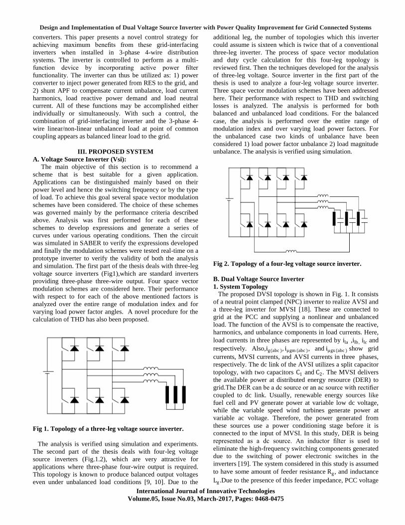
and simulation. The first part of the thesis deals with three-leg
voltage source inverters (Fig1),which are standard inverters
providing three-phase three-wire output. Four space vector
modulation schemes are considered here. Their performance
with respect to for each of the above mentioned factors is
analyzed over the entire range of modulation index and for
varying load power factor angles. A novel procedure for the
calculation of THD has also been proposed.
Fig 1. Topology of a three-leg voltage source inverter.
The analysis is verified using simulation and experiments.
The second part of the thesis deals with four-leg voltage
source inverters (Fig.1.2), which are very attractive for
applications where three-phase four-wire output is required.
This topology is known to produce balanced output voltages
even under unbalanced load conditions [9, 10]. Due to the
additional leg, the number of topologies which this inverter
could assume is sixteen which is twice that of a conventional
three-leg inverter. The process of space vector modulation
and duty cycle calculation for this four-leg topology is
reviewed first. Then the techniques developed for the analysis
of three-leg voltage. Source inverter in the first part of the
thesis is used to analyze a four-leg voltage source inverter.
Three space vector modulation schemes have been addressed
here. Their performance with respect to THD and switching
losses is analyzed. The analysis is performed for both
balanced and unbalanced load conditions. For the balanced
case, the analysis is performed over the entire range of
modulation index and over varying load power factors. For
the unbalanced case two kinds of unbalance have been
considered 1) load power factor unbalance 2) load magnitude
unbalance. The analysis is verified using simulation.
Fig 2. Topology of a four-leg voltage source inverter.
B. Dual Voltage Source Inverter
1. System Topology
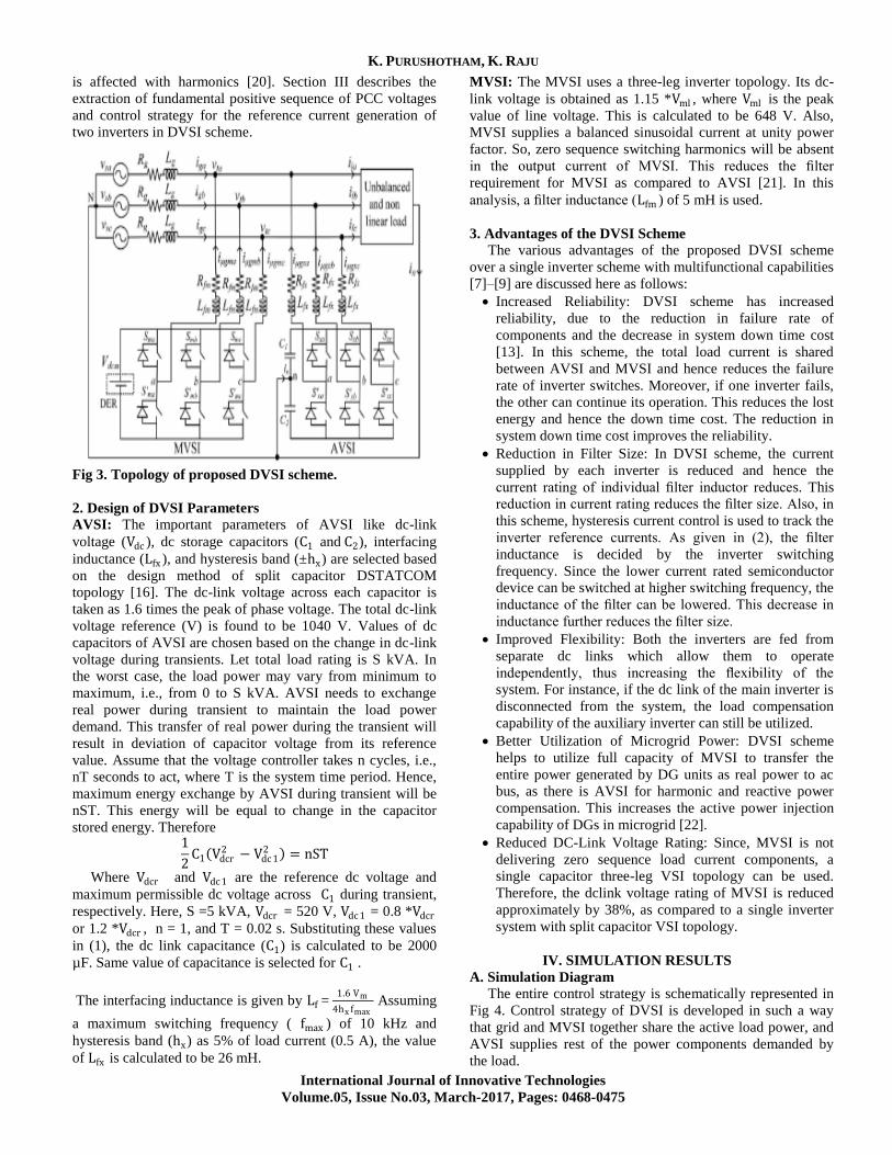
The proposed DVSI topology is shown in Fig. 1. It consists
of a neutral point clamped (NPC) inverter to realize AVSI and
a three-leg inverter for MVSI [18]. These are connected to
grid at the PCC and supplying a nonlinear and unbalanced
load. The function of the AVSI is to compensate the reactive,
harmonics, and unbalance components in load currents. Here,
load currents in three phases are represented by ila ,ilb , ilc and
respectively. Also,ig(abc ), iμgm (abc ), and iμgx (abc ) show grid
currents, MVSI currents, and AVSI currents in three phases,
respectively. The dc link of the AVSI utilizes a split capacitor
topology, with two capacitors C1 and C2. The MVSI delivers
the available power at distributed energy resource (DER) to
grid.The DER can be a dc source or an ac source with rectifier
coupled to dc link. Usually, renewable energy sources like
fuel cell and PV generate power at variable low dc voltage,
while the variable speed wind turbines generate power at
variable ac voltage. Therefore, the power generated from
these sources use a power conditioning stage before it is
connected to the input of MVSI. In this study, DER is being
represented as a dc source. An inductor filter is used to
eliminate the high-frequency switching components generated
due to the switching of power electronic switches in the
inverters [19]. The system considered in this study is assumed
to have some amount of feeder resistance Rg , and inductance
Lg .Due to the presence of this feeder impedance, PCC voltage
K. PURUSHOTHAM, K. RAJU
International Journal of Innovative Technologies
Volume.05, Issue No.03, March-2017, Pages: 0468-0475
is affected with harmonics [20]. Section III describes the
extraction of fundamental positive sequence of PCC voltages
and control strategy for the reference current generation of
two inverters in DVSI scheme.
Fig 3. Topology of proposed DVSI scheme.
2. Design of DVSI Parameters
AVSI: The important parameters of AVSI like dc-link
voltage (Vdc ), dc storage capacitors (C1 and C2), interfacing
inductance (Lfx ), and hysteresis band (±hx) are selected based
on the design method of split capacitor DSTATCOM
topology [16]. The dc-link voltage across each capacitor is
taken as 1.6 times the peak of phase voltage. The total dc-link
voltage reference (V) is found to be 1040 V. Values of dc
capacitors of AVSI are chosen based on the change in dc-link
voltage during transients. Let total load rating is S kVA. In
the worst case, the load power may vary from minimum to
maximum, i.e., from 0 to S kVA. AVSI needs to exchange
real power during transient to maintain the load power
demand. This transfer of real power during the transient will
result in deviation of capacitor voltage from its reference
value. Assume that the voltage controller takes n cycles, i.e.,
nT seconds to act, where T is the system time period. Hence,
maximum energy exchange by AVSI during transient will be
nST. This energy will be equal to change in the capacitor
stored energy. Therefore 1
2C1 Vdcr
2 − Vdc 12 = nST
Where Vdcr and Vdc 1 are the reference dc voltage and
maximum permissible dc voltage across C1 during transient,
respectively. Here, S =5 kVA, Vdcr = 520 V, Vdc 1 = 0.8 *Vdcr
or 1.2 *Vdcr , n = 1, and T = 0.02 s. Substituting these values
in (1), the dc link capacitance (C1) is calculated to be 2000
µF. Same value of capacitance is selected for C1 .
The interfacing inductance is given by Lf = 1.6 Vm
4hx fmax Assuming
a maximum switching frequency ( fmax ) of 10 kHz and
hysteresis band (hx) as 5% of load current (0.5 A), the value
of Lfx is calculated to be 26 mH.
MVSI: The MVSI uses a three-leg inverter topology. Its dc-
link voltage is obtained as 1.15 *Vml , where Vml is the peak
value of line voltage. This is calculated to be 648 V. Also,
MVSI supplies a balanced sinusoidal current at unity power
factor. So, zero sequence switching harmonics will be absent
in the output current of MVSI. This reduces the filter
requirement for MVSI as compared to AVSI [21]. In this
analysis, a filter inductance (Lfm ) of 5 mH is used.
3. Advantages of the DVSI Scheme The various advantages of the proposed DVSI scheme
over a single inverter scheme with multifunctional capabilities
[7]–[9] are discussed here as follows:
Increased Reliability: DVSI scheme has increased
reliability, due to the reduction in failure rate of
components and the decrease in system down time cost
[13]. In this scheme, the total load current is shared
between AVSI and MVSI and hence reduces the failure
rate of inverter switches. Moreover, if one inverter fails,
the other can continue its operation. This reduces the lost
energy and hence the down time cost. The reduction in
system down time cost improves the reliability.
Reduction in Filter Size: In DVSI scheme, the current
supplied by each inverter is reduced and hence the
current rating of individual filter inductor reduces. This
reduction in current rating reduces the filter size. Also, in
this scheme, hysteresis current control is used to track the
inverter reference currents. As given in (2), the filter
inductance is decided by the inverter switching
frequency. Since the lower current rated semiconductor
device can be switched at higher switching frequency, the
inductance of the filter can be lowered. This decrease in
inductance further reduces the filter size.
Improved Flexibility: Both the inverters are fed from
separate dc links which allow them to operate
independently, thus increasing the flexibility of the
system. For instance, if the dc link of the main inverter is
disconnected from the system, the load compensation
capability of the auxiliary inverter can still be utilized.
Better Utilization of Microgrid Power: DVSI scheme
helps to utilize full capacity of MVSI to transfer the
entire power generated by DG units as real power to ac
bus, as there is AVSI for harmonic and reactive power
compensation. This increases the active power injection
capability of DGs in microgrid [22].
Reduced DC-Link Voltage Rating: Since, MVSI is not
delivering zero sequence load current components, a
single capacitor three-leg VSI topology can be used.
Therefore, the dclink voltage rating of MVSI is reduced
approximately by 38%, as compared to a single inverter
system with split capacitor VSI topology.
IV. SIMULATION RESULTS
A. Simulation Diagram
The entire control strategy is schematically represented in
Fig 4. Control strategy of DVSI is developed in such a way
that grid and MVSI together share the active load power, and
AVSI supplies rest of the power components demanded by
the load.
Design and Implementation of Dual Voltage Source Inverter with Power Quality Improvement for Grid Connected Systems
International Journal of Innovative Technologies
Volume.05, Issue No.03, March-2017, Pages: 0468-0475
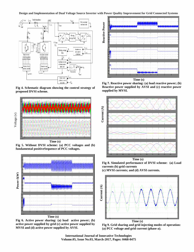
Fig 4. Schematic diagram showing the control strategy of
proposed DVSI scheme.
Time (s)
Fig 5. Without DVSI scheme: (a) PCC voltages and (b)
fundamental positiveSequence of PCC voltages.
Time (s)
Fig 6. Active power sharing: (a) load active power; (b)
active power supplied by grid (c) active power supplied by
MVSI and (d) active power supplied by AVSI.
Time (s)
Fig 7. Reactive power sharing: (a) load reactive power; (b)
Reactive power supplied by AVSI and (c) reactive power
supplied by MVSI.
Time (s)
Fig 8. Simulated performance of DVSI scheme: (a) Load
currents (b) grid currents
(c) MVSI currents; and (d) AVSI currents.
Time (s)
Fig 9. Grid sharing and grid injecting modes of operation:
(a) PCC voltage and grid current (phase-a).
Vo
ltag
e (v
) P
ow
er (
kW
)
Rea
ctiv
e P
ow
er
(kV
Ar)
Cu
rren
t (A
) C
urr
en
t (A
)
K. PURUSHOTHAM, K. RAJU
International Journal of Innovative Technologies
Volume.05, Issue No.03, March-2017, Pages: 0468-0475
Time (s)
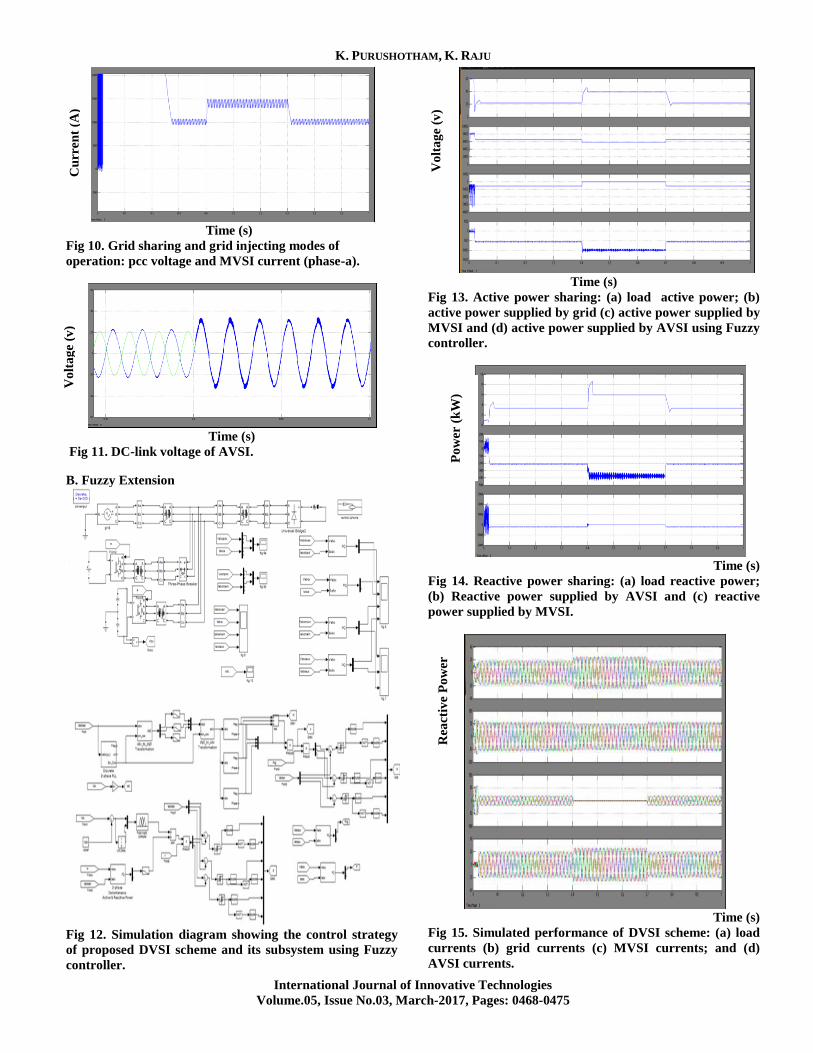
Fig 10. Grid sharing and grid injecting modes of
operation: pcc voltage and MVSI current (phase-a).
Time (s)
Fig 11. DC-link voltage of AVSI.
B. Fuzzy Extension
Fig 12. Simulation diagram showing the control strategy
of proposed DVSI scheme and its subsystem using Fuzzy
controller.
Time (s)
Fig 13. Active power sharing: (a) load active power; (b)
active power supplied by grid (c) active power supplied by
MVSI and (d) active power supplied by AVSI using Fuzzy
controller.
Time (s)
Fig 14. Reactive power sharing: (a) load reactive power;
(b) Reactive power supplied by AVSI and (c) reactive
power supplied by MVSI.
Time (s)
Fig 15. Simulated performance of DVSI scheme: (a) load
currents (b) grid currents (c) MVSI currents; and (d)
AVSI currents.
Vo
lta
ge
(v)
Cu
rren
t (A
)
Vo
lta
ge
(v)
Po
wer
(k
W)
Rea
ctiv
e P
ow
er
(kV
Ar)
Design and Implementation of Dual Voltage Source Inverter with Power Quality Improvement for Grid Connected Systems
International Journal of Innovative Technologies
Volume.05, Issue No.03, March-2017, Pages: 0468-0475
Time (s)
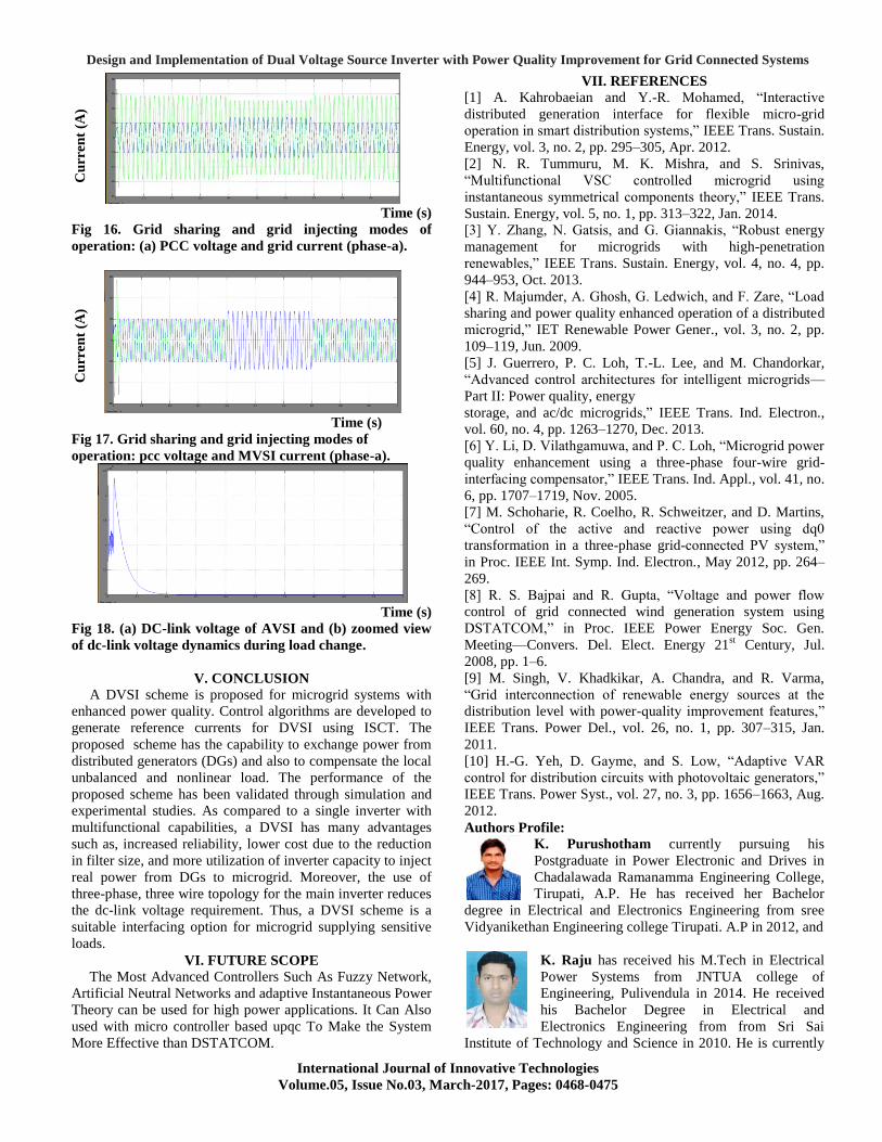
Fig 16. Grid sharing and grid injecting modes of
operation: (a) PCC voltage and grid current (phase-a).
Time (s)
Fig 17. Grid sharing and grid injecting modes of
operation: pcc voltage and MVSI current (phase-a).
Time (s)
Fig 18. (a) DC-link voltage of AVSI and (b) zoomed view
of dc-link voltage dynamics during load change.
V. CONCLUSION
A DVSI scheme is proposed for microgrid systems with
enhanced power quality. Control algorithms are developed to
generate reference currents for DVSI using ISCT. The
proposed scheme has the capability to exchange power from
distributed generators (DGs) and also to compensate the local
unbalanced and nonlinear load. The performance of the
proposed scheme has been validated through simulation and
experimental studies. As compared to a single inverter with
multifunctional capabilities, a DVSI has many advantages
such as, increased reliability, lower cost due to the reduction
in filter size, and more utilization of inverter capacity to inject
real power from DGs to microgrid. Moreover, the use of
three-phase, three wire topology for the main inverter reduces
the dc-link voltage requirement. Thus, a DVSI scheme is a
suitable interfacing option for microgrid supplying sensitive
loads.
VI. FUTURE SCOPE
The Most Advanced Controllers Such As Fuzzy Network,
Artificial Neutral Networks and adaptive Instantaneous Power
Theory can be used for high power applications. It Can Also
used with micro controller based upqc To Make the System
More Effective than DSTATCOM.
VII. REFERENCES
[1] A. Kahrobaeian and Y.-R. Mohamed, ―Interactive
distributed generation interface for flexible micro-grid
operation in smart distribution systems,‖ IEEE Trans. Sustain.
Energy, vol. 3, no. 2, pp. 295–305, Apr. 2012.
[2] N. R. Tummuru, M. K. Mishra, and S. Srinivas,
―Multifunctional VSC controlled microgrid using
instantaneous symmetrical components theory,‖ IEEE Trans.
Sustain. Energy, vol. 5, no. 1, pp. 313–322, Jan. 2014.
[3] Y. Zhang, N. Gatsis, and G. Giannakis, ―Robust energy
management for microgrids with high-penetration
renewables,‖ IEEE Trans. Sustain. Energy, vol. 4, no. 4, pp.
944–953, Oct. 2013.
[4] R. Majumder, A. Ghosh, G. Ledwich, and F. Zare, ―Load
sharing and power quality enhanced operation of a distributed
microgrid,‖ IET Renewable Power Gener., vol. 3, no. 2, pp.
109–119, Jun. 2009.
[5] J. Guerrero, P. C. Loh, T.-L. Lee, and M. Chandorkar,
―Advanced control architectures for intelligent microgrids—
Part II: Power quality, energy
storage, and ac/dc microgrids,‖ IEEE Trans. Ind. Electron.,
vol. 60, no. 4, pp. 1263–1270, Dec. 2013.
[6] Y. Li, D. Vilathgamuwa, and P. C. Loh, ―Microgrid power
quality enhancement using a three-phase four-wire grid-
interfacing compensator,‖ IEEE Trans. Ind. Appl., vol. 41, no.
6, pp. 1707–1719, Nov. 2005.
[7] M. Schoharie, R. Coelho, R. Schweitzer, and D. Martins,
―Control of the active and reactive power using dq0
transformation in a three-phase grid-connected PV system,‖
in Proc. IEEE Int. Symp. Ind. Electron., May 2012, pp. 264–
269.
[8] R. S. Bajpai and R. Gupta, ―Voltage and power flow
control of grid connected wind generation system using
DSTATCOM,‖ in Proc. IEEE Power Energy Soc. Gen.
Meeting—Convers. Del. Elect. Energy 21st Century, Jul.
2008, pp. 1–6.
[9] M. Singh, V. Khadkikar, A. Chandra, and R. Varma,
―Grid interconnection of renewable energy sources at the
distribution level with power-quality improvement features,‖
IEEE Trans. Power Del., vol. 26, no. 1, pp. 307–315, Jan.
2011.
[10] H.-G. Yeh, D. Gayme, and S. Low, ―Adaptive VAR
control for distribution circuits with photovoltaic generators,‖
IEEE Trans. Power Syst., vol. 27, no. 3, pp. 1656–1663, Aug.
2012.
Authors Profile:
K. Purushotham currently pursuing his
Postgraduate in Power Electronic and Drives in
Chadalawada Ramanamma Engineering College,
Tirupati, A.P. He has received her Bachelor
degree in Electrical and Electronics Engineering from sree
Vidyanikethan Engineering college Tirupati. A.P in 2012, and
K. Raju has received his M.Tech in Electrical
Power Systems from JNTUA college of
Engineering, Pulivendula in 2014. He received
his Bachelor Degree in Electrical and
Electronics Engineering from from Sri Sai
Institute of Technology and Science in 2010. He is currently
Cu
rren
t (A
) C
urr
en
t (A
)

K. PURUSHOTHAM, K. RAJU
International Journal of Innovative Technologies
Volume.05, Issue No.03, March-2017, Pages: 0468-0475
working as a Assistant Professor in Department of Electrical
and Electronics Engineering, Chadalawada Ramanamma
Engineering College, Tirupati, A.P. His area of interests are
Deregulated Power System,,power System Stability.