design and testing of a communications educational ...jmconrad/gradstudents/thesis_vakil.pdf ·...
TRANSCRIPT

DESIGN AND TESTING OF A COMMUNICATIONS EDUCATIONAL
EMBEDDED BOARD FOR TEACHING AND RESEARCH
by
Ishfan Vakil
A thesis submitted to the faculty of
The University of North Carolina at Charlotte
in partial fulfillment of the requirements
for the degree of Master of Science in the
Department of Electrical and Computer Engineering
Charlotte
2006
Approved by:
______________________________
Dr. James M. Conrad
______________________________
Dr. Ivan L. Howitt
______________________________
Dr. Thomas P. Weldon

ii
© 2006
Ishfan Vakil
ALL RIGHTS RESERVED

iii
DEDICATION
To my parents for their endless love and support.

iv
ABSTRACT
ISHFAN VAKIL. Design and testing of a communications educational embedded board
for teaching and research. (Under the direction of DR JAMES M. CONRAD)
A communications educational embedded system board has been designed and tested for
use in teaching and research. The motivation lies in the desire to design a board capable
of data communication using optical fiber, infrared, serial RS-232 and USB. The board
will be used for research and teaching purposes in the field of embedded systems. There
has been significant technological development in the field of data communications.
Many embedded systems which are integrated as a part of many high technology devices
and home appliances use the most recently developed and advanced means of data
communication for faster and reliable data transfer. Optical communication using either
optical fiber or infrared have been widely used in industry and integrated into modern
devices for efficient and faster data communication. The embedded systems engineer
needs to have the knowledge about the working of such data communication
technologies. The main aim of this project is to develop a communication board which
handles data communication using optical fiber and Infrared. The board can be used in
class room teaching for learning embedded systems and at the same time give the
embedded systems engineering student the hands on experience to handle optical
communication.

v
ACKNOWLEDGEMENTS
As with any endeavor, this research project could not have been completed without the
help and support of others. Foremost, I wish to thank my research advisor Dr James M.
Conrad for his guidance throughout the course of this thesis. Without his efforts and
guidance this thesis would have never been completed. His systematic approach and
management skills along with encouragement at every step of this thesis were some of
the major factors behind the completion of this thesis work.
I would also like to thank Dr. Ivan L. Howitt and Dr. Thomas P. Weldon for
reviewing this thesis and for further instructions and suggestions for improving the thesis.
I am greatly indebted to the members of the embedded systems research lab. Sandeep
Sirpatil has a vast wealth of knowledge that he is very willing to share, Gajendra Singh,
Gurudat Mysore and Sonia Thakur were fun to work with and also contributed some
good ideas to my thesis. In addition, several other people outside the project provided
necessary diversions and insight along the road. For her administrative support, Pat
Winter receives my sincere gratitude.
I would also like to thank the Charlotte Research Institute and Optics center for
their generous financial support. And, in general, I would like to thank my professors and
fellow students/colleagues here at University of North Carolina at Charlotte they have
consistently been of high caliber and it was a pleasure working with you all. Finally, I
would like to thank my family and friends for their support and encouragement.

vi
TABLE OF CONTENTS
DEDICATION.................................................................................................................. iii
ABSTRACT...................................................................................................................... iv
ACKNOWLEDGEMENTS ............................................................................................. v
TABLE OF CONTENTS ................................................................................................ vi
LIST OF FIGURES ......................................................................................................... ix
LIST OF TABLES .......................................................................................................... xii
LIST OF ABREVATIONS ........................................................................................... xiii
CHAPTER 1: INTRODUCTION.................................................................................... 1
1.1 Introduction to the Thesis ...................................................................................... 1
1.2 Work done in the past............................................................................................. 3
1.3 Motivation................................................................................................................ 5
1.4 Organization of Thesis............................................................................................ 7
CHAPTER 2: BOARD DESIGN ..................................................................................... 9
2.1 Board Specification................................................................................................. 9
2.2 Board Functionalities............................................................................................ 10
CHAPTER 3: HARDWARE ......................................................................................... 12
3.1 Microcontroller ..................................................................................................... 12
3.2 Optical Fiber Transmitter and Receiver ............................................................ 18
3.3 Infrared Transceiver ............................................................................................ 21
3.4 Serial RS-232 ......................................................................................................... 23
3.4 Serial USB.............................................................................................................. 28

vii
3.5 Other Hardware.................................................................................................... 33
3.5.1 LCD module ................................................................................................... 33
3.5.2 Switches and LEDs ........................................................................................ 34
CHAPTER 4: INTERFACING AND SCHEMATIC DESIGN ................................. 36
4.1 Overview of OrCAD Capture .............................................................................. 36
4.2 Microcontroller Circuit ........................................................................................ 38
4.2 Optical Communication Circuit. ......................................................................... 40
4.3 Serial RS-232 Circuit ............................................................................................ 44
4.4 Serial USB Circuit................................................................................................. 45
4.5 Power Circuit ........................................................................................................ 48
4.6 Circuit for On Board LCD Screen ...................................................................... 50
4.7 Circuit for debugging LEDs and Switches ......................................................... 51
CHAPTER 5: TESTING ................................................................................................ 53
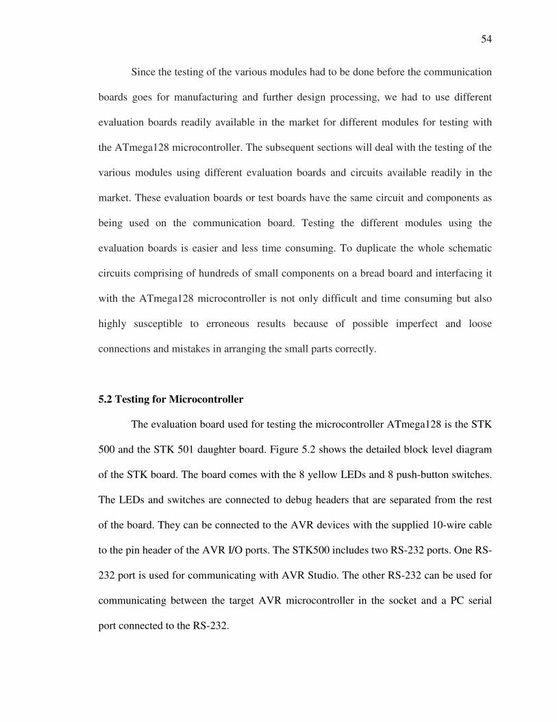
5.2 Testing for Microcontroller ................................................................................. 54
5.3 Testing for Optical Fiber Transceiver ................................................................ 57
5.4 Testing for Serial USB .......................................................................................... 60
CHAPTER 6: LAYOUT DESIGN ................................................................................ 62
6.1 Overview ................................................................................................................ 62
6.2 Design of New Footprints ..................................................................................... 63
CHAPTER 7: CONCLUSION AND FUTURE WORK ............................................. 69
REFERENCES................................................................................................................ 72
APPENDIX A: SCHEMATIC ....................................................................................... 74
SCHEMATIC: MICROCONTROLLER, JTAG AND I/O PORTS .................... 74
viii
SCHEMATIC: OPTICAL FIBER TRANSMITTER- RECIEVER AND ............ 75
INFRARED TRANSCIEVER ................................................................................... 75
SCHEMATIC: POWER SUPPLY ............................................................................ 76
SCHEMATIC: RS-232 PORT AND LCD ................................................................ 77
SCHEMATIC: USB CONNECTOR INTERFACE ................................................ 78
APPENDIX B: BILL OF MATERIALS (BOM) ......................................................... 79
APPENDIX C: TEST CODE ......................................................................................... 82
APPENDIX D: SAMPLE LAB EXERCISES .............................................................. 89

ix
LIST OF FIGURES
FIGURE 2.1: Diagram of the Embedded Communication Board. 9
FIGURE 3. 1: Quad flat pack 64 pin ATmega128L. 12
FIGURE 3. 2: Block Diagram of ATmega128L. 13
FIGURE 3. 3: AVR® JTAGICE mkII. 16
FIGURE 3. 4 : Pin Diagram of ATmega128L. 17
FIGURE 3. 5: HFBR-14xx and HFBR-24xx package. 18
FIGURE 3. 6: HFBR 14x 2 Transmitters. 19
FIGURE 3. 7: HFBR 24x2Receiver. 20
FIGURE 3. 8: TFDU4100 Infrared Transceiver package. 21
FIGURE 3. 9: Functional Block Diagram of TFDU4100. 22
FIGURE 3. 10: PIN configuration of a DB9 connector for RS-232 port. 24
FIGURE 3. 11: MAX202 Pin Configuration and Typical Operating Circuit. 26
FIGURE 3. 12: Dual Charge pump inside the MAX202 transceiver. 27
FIGURE 3. 13: Functional block diagram of FT232BM USB to serial IC. 29
FIGURE 3. 14: FT232BM pin out and schematic symbol. 31
FIGURE 3. 15: Mini USB B connector. 32
FIGURE 3. 16: ACM0802 LCD Module. 33
FIGURE 3. 17: 4mm J hook surface mount switch. 34
FIGURE 3. 18:Surface mount 635nm LED. 35
FIGURE 4. 1: Capture design window. 38
FIGURE 4. 2: I/O connector sockets for future hardware interface. 39
FIGURE 4. 3: JTAG 10 pin connector schematic. 39

x
FIGURE 4. 4: Typical Circuit configuration for HFBR 14xx and HFBR 24xx. 40
FIGURE 4. 5: Optical fiber transmitter HFBR 1412 schematic. 41
FIGURE 4. 6: Optical fiber Receiver HFBR 2412 schematic. 42
FIGURE 4. 7: Recommended circuit for TFDU4100 Transceiver. 43
FIGURE 4. 8: TFDU4100 Infra red Transceiver Schematic. 44
FIGURE 4. 9: The DB9 connector and the serial driver ICMAX202 for serial interface 45
FIGURE 4. 10: USB mini B connector interface with FT232BM driver IC. 46
FIGURE 4. 11: A two pin ceramic crystal configuration with the FT232BM driver IC. 47
FIGURE 4.12: EEPROM 93C46 configuration with the FT232BM driver IC. 47
FIGURE 4. 13: Schematic showing the DC jack and the sliding switch. 49
FIGURE 4. 14: Schematic of the rectifier bridge and the 7805 voltage regulator. 49
FIGURE 4.15: Schematic of the 7805 voltage regulator. 50
FIGURE 4.16: Schematic showing the LCD module. 51
FIGURE 4.17: Schematic showing LEDs and Switches. 52
FIGURE 5.1: The setup to program AVR microcontroller using JTAG ICE. 53
FIGURE 5.2: The components of the STK500 board. 55
FIGURE 5.3: The STK500 board with default settings. 56
FIGURE 5.4: The STK501 board with the socket to hold the ATmega128. 56
FIGURE 5.5: The Agilent HFBR 04x series Optical Fiber evaluation kit. 58
FIGURE 5.6: Block Diagram showing testing of Optical fiber module. 59
FIGURE 5.7: USB to Serial converter used for testing the USB circuit. 60
FIGURE 6.1: ORCAD Layout foot print: RS-232 Serial Port. 64
FIGURE 6.2: ORCAD Layout foot print: ATmega128 microcontroller. 65
xi
FIGURE 6.3: ORCAD Layout foot print: USB to serial IC driver chip (FT232BM). 65
FIGURE 6.4: ORCAD Layout foot print: 2 Pin Crystal Oscillator. 66
FIGURE 6.5: ORCAD Layout foot print: 4 Pin Crystal Oscillator. 66
FIGURE 6.6: ORCAD Layout foot print: Serial UART transceiver IC (MAX202). 67
FIGURE 6.7: ORCAD Layout foot print: Surface mount Bridge rectifier (DF10S). 67
FIGURE 6.8: ORCAD Layout foot print: USB mini B port. 68

xii
LIST OF TABLES
TABLE 3. 1: Pin description TFDU4100 23
TABLE 3. 2: Voltage limits of RS-232 25
TABLE 3. 3: USB Mini B connector Pin functionality 33
TABLE 3. 4: ACM0802 LCD Pin functionality 34

xiii
LIST OF ABREVATIONS
ALU Arithmetic Logic Unit
ATmega 128L AVR ATMEL 8 bit Microcontroller
AVR RISC Microcontroller family from ATMEL.
ADC Analog to Digital Converter.
BOM Bill of Materials
CISC Complex Instruction Set Computing
DRC Design Rule Check
EEPROM Electrically Erasable Programmable Read only Memory
EMI Electro Magnetic Induction
FT232BM USB to Serial Transceiver IC
FIFO First In First Out
HFBR Agilent Technologies Optical Fiber Transceivers
I/O Input/Output
IR Infrared
IDE Integrated Development Environment
JTAG Joint Test Action Group
KBPS Kilo bytes per second
LCD Liquid Crystal Display
MBPS Mega bytes per second
MAX202 RS-232 transceiver IC
NRZI Non Return to Zero, Inverted.
PWM Pulse Width Modulation.

xiv
RS-232 Standard for Serial communication
RISC Reduced Instruction Set Computing
RTC Real Time Counter.
RS Recommended Standards.
RWW Read While Write.
SIR Serial Infrared
SIE Serial Interface Engine.
TFDU4100 Vishay Semiconductors Infar Red Transceivers
UART Universal Asynchronous Receiver Transmitter
USB Universal Serial Bus
CHAPTER 1: INTRODUCTION
1.1 Introduction to the Thesis
Data communication is one of the most important and fundamental part of any
electronic or electric equipment in use today. Transfer of data in the form of radio waves,
voltages and light signals is taking place all around us. Two parts of the same electrical
equipment controlling a given process send and receive control signals in the form of
electrical data. Control systems that are embedded inside industrial grade high
technology equipment or as a part of many household electrical appliances require data
communication either within the system, between the various components involved in
that system or outside the system. It would be safe to say that data communication forms
the backbone for any electronic system. Data may be carried to a distance of less than a
fraction of an inch on a printed circuit board to as far as a few hundred miles through
long wires. Different devices based on the requirements and the type of device use
different methods of data communication. The basic aim of each device capable of data
communications is to transmit and/or receive data at the highest possible transmission
speed with the lowest possible transmission error, consume lowest possible power, and
cost the least amount of money possible.
Data is transmitted through communication channels, which are pathways through
which data flows from the transmitter to the receiver. Communication channels can vary
depending upon the type of application and the transmission requirements. They can be
either wire line or wireless channels. The wire line communication channels physically
connect the transmitter to the receiver with a wire which could be a twisted pair, a coaxial
2
cable or an optical fiber. The wireless communication channel requires no physical
connection between the transmitter and the receiver. Data is transmitted through air
where the transmitter having an antenna radiates signals that can be received by another
antenna at the receiving end.
The speed with which data can be transmitted between a transmitter and a
receiver is called data transfer speed or simply data rate. In a digital communication
channel, the data is represented by individual bits which may be combined to form
multibit message units. A byte, which consists of eight bits, is an example of a message
unit that data rates are measured in megabytes per second (Mbps), kilobytes per second
(Kbps) or simply bytes per second (bps). The data transfer rate or simply data rate is also
termed as throughput. The throughput of a device would thus be defined as the number of
data bits transferred per second.
Embedded system is one of the fields where data communication holds a very
important place. Embedded communication devices are integrated into different
applications ranging from homeland security system to industry automation to simple
home appliances. With these significant technological advancements in the field of data
communication and the subsequent development of high technology equipment and
gadgets comes the need for teaching the latest technology in data communication to the
upcoming engineering students. Embedded system engineers have knowledge about
computer architecture, microcontrollers and programming. The demand of embedded
engineers having knowledge about data communication is going to be high. However
there are very few development tools available for classroom teaching, so the engineering
students usually do not learn much about different data communication technologies.
3
1.2 Work done in the past
Before the start of this thesis, much time was spent in understanding the basic
requirements and need of the students to work with communication modules like the one
being designed and tested. A lot of work has been done in the past to understand the
learning curve of students working in embedded systems and how different lab exercises
directly related to programming of the embedded microcontroller board along with
communication modules like infrared and optical fiber helps them to better understand
the subject of embedded systems programming, embedded systems hardware
requirements and data communication.
Several papers related to the software and hardware tools for teaching
communication and embedded systems concepts have been written by experienced
faculties, who have been involved in teaching embedded systems and communication
systems for several years.
One of the works worth mentioning is the research effort by Conrad and Howitt
on software and hardware tools for teaching communication concepts and introducing
students to low power wireless communication [12]. In this effort, the experiences of
introducing board to board communication concepts and hardware to students have been
covered. Communication concepts using optical fiber, infrared and low power wireless
communication was introduced to students and the effort of the students was assessed
based on the success of their assigned work.
Other major work done in the Department of Electrical and Computer
Engineering, University of North Carolina at Charlotte was the introduction of optical

4
communication in the embedded systems course [6]. The students were made to do lab
exercises on optical fiber and infrared communication and results were collected based on
the speed of data transfer and other communication related concepts. More than 20
students were involved in various lab exercises which gave the researchers a thorough
idea about the concept of introducing such labs into courses like embedded systems and
how these exercises help the students to further strengthen their embedded systems
programming , embedded systems hardware and communication theory concepts.
In one of the lab exercises performed by the students, throughput measurements
were done under different conditions. The requirement was to push the optical fiber
communication to its limit by using simple I/O interfacing in contrast to interfacing with
the UART of the microcontroller. Data was collected from the different teams of students
and compared. Results showed that speeds higher than expected through UART could be
achieved using programmed I/O pins however with a compromise of increasing error
rates.
Many related work in this field have shown that introducing experimental or lab
related concepts in a teaching course improves the way a student learns about that subject
[11]. Communication theory and analytical models are often considered dry by students,
leading to poor retention of the material. Understanding these concepts is an important
part of understanding approaches required to solve real world problems. Therefore, one
of the goals of this research is to develop hands-on learning modules for communications
courses. There is a substantial body of work relating to the advantages and approaches for
integrating course work with laboratory investigation [16-23] in order to illustrate
concepts in communications. Of particular interest is the three-level approach [16-18]

5
where the student is introduced to 1) component level, 2) sub-system level and then 3)
system level experiments. It is anticipated this approach will be adopted for courses that
use this communications hub board, and is one of the primary motivations for developing
this board. The optical communication board will be the only microcontroller board and
the first of its kind having optical fiber, infrared, USB and RS232 in one package that
will be available for students
1.3 Motivation
The primary motivation for this work was the lack of commercially available low
cost microcontroller boards that would have all the communication modules or
components interfaced on it. Having a single board simplifies the design and reduces the
need of using several different boards and components for performing research and
experiments. The board being further used as a platform for teaching and learning
embedded systems. Reducing the cost of the board as much as possible was one of the
main design objectives. The target user groups for the communication board are the
students and researchers in various universities and research labs.
The other design objectives were robustness, reliability and functionality of the board.
Most of the early technological learners such as high school students lack experience and
expert knowledge for interfacing a controller board with other components. To prevent
the learners from making errors, connectors on our board have been made foolproof (the
user cannot damage the components of the board by plugging cables in the wrong
sockets).

6
After reviewing the commercially available micro-controller boards with respect
to their suitability as teaching tools, we concluded that none of the existing micro-
controller boards met our requirements. We then designed a new controller board based
on previous boards and added various communication modules to it.
The major uses of this embedded systems communication board can be
summarized as follows:
• The board will be used as a teaching tool in embedded systems courses.
• The embedded systems course will cover the basic microcontroller
programming and hardware details related to the board.
• Laboratory exercises form an essential part of any embedded system or
communication course. This board will serve as basic learning module for the
students performing programming, testing and other interfacing exercises in the
lab.
• Research in the field of optical fiber and infrared communication can be
performed on the basic level using this board. Measurement of the throughputs
and calculating the maximum throughputs at different speeds and in different
conditions can be an excellent research issue to work upon.
• Interfacing of different sensors on the board will allow the user to accumulate
data from the sensor and transmit it through optical fiber over long distances of
up to 2.7 Km.
• The board will provide enough resources for the researchers and developers to
build applications on top of it by interfacing different technologies with it.

7
1.4 Organization of Thesis
The thesis has been organized into different sections for the ease of reading and
understanding. Care has been taken to follow a particular pattern in such a way that
things which are relevant at the beginning and are required to understand the later
chapters have been discussed in the first few chapters. A reader having very little
knowledge about the subject can easily follow the chapters and understand the details in
the subsequent chapters.
Chapter 2 of the thesis provides a detail into the understanding of the
specifications and functionalities that were required for the board. The entire design rests
on the initial specifications set for the project. All throughout the design project these
specifications and required functionalities were followed and kept in mind.
Chapter 3 of the thesis provides the details of the hardware used for the board
design. The hardware detail of each module of the communication board has been
discussed in this chapter. The specifications of the microcontroller followed by the
hardware details of the optical communication modules and in the end the hardware
details of the serial RS-232 and serial USB have been discussed in detail.
The Chapter 4 is the most important chapter of the thesis reflecting the maximum
amount of work done on the project. The design details of each circuit, including the
schematic design, have been discussed in this chapter. The entire design of the
communication board has been divided into a number of important circuits for the ease of
design and understanding. Each of these circuits has been discussed along with the
interfacing techniques used. The interfacing of each module with the micro controller has
been discussed in detail.

8
Chapter 5 of the thesis provides the details about the testing of the different
modules used in the communication board. Each of the board modules was tested for its
design correction and functionality. Testing forms a very important part of the project.
The project can only go to the next stage of layout design and finally manufacturing if the
test results are correct and favor the design.
Chapter 6 provides a small introduction to the layout specifications of the board
and various footprints of some important modules of the board. This chapter discusses the
importance of proper layout design for manufacturing of flawless microcontroller boards.
Chapter 7 of the thesis summarizes and concludes the work done in this project
and discusses the future work needed on this project.

9
CHAPTER 2: BOARD DESIGN
2.1 Board Specification
The Communication Educational Board is a small sized communication
hub capable of handling different types of data communication. Optical fiber, infrared,
RS-232 and USB are some of the modules which can handle data communication on the
board. Each of these modules is independent of each other and works at different baud
rates depending upon their specification. The board is powered through a DC voltage
supply between 9V to 15V. The board carries a voltage regulator which brings down the
voltage to 5V. The board can also be alternatively powered through the USB port, giving
the port additional functionality.
Figure 2.1: Diagram of the Embedded Communication Board
All the components on the board have been chosen in order to fit the voltage
requirements. To make the board work as a low power communication hub, low power

10
consuming devices including the microcontroller have been chosen with no or very less
compromise with the price.
The components have been chosen such that the size of the overall board does
not increase beyond 4 square inches. Surface mount resistors and capacitors of standard
size 0603(~1.6 mm) have been chosen. These components immensely reduce the over all
complexity and the size of the board. The board has been equipped with a LCD screen,
giving it an additional user friendly look. Baud rates, bit error and/or current state of the
microcontroller are some of the things that can be displayed on the LCD screen by
programming the board. The board comes along with a number of test and sample codes
which can be downloaded on the board through the PC using a JTAG connector. The test
codes will be able to test the functionality of each module on the board. A user will be
able to alter and improve upon those test codes depending upon the requirement.
2.2 Board Functionalities
Before the design of the board was started we had to decide upon the different
data communication modules that will be used on the communication educational board.
The optical communication transceivers, which include both fiber optic and infrared
transceivers, form the main data communication ports on the board. The entire board has
been initially designed based upon these two data communication channels. However
apart from the optical communication, the board will be capable of handling serial data
communication through the serial RS-232 port. In addition to the serial port a USB port
has also been provided. The USB port will be capable of handling data communication
and in addition provide an alternate power source to the board. The JTAG (Joint Test
11
Action Group) interface present on the board is used for downloading code from the PC
to program the microcontroller. The Board has been designed specifically for
educational and research purposes. The board functionalities can be used to demonstrate
data communication in embedded system or optical communication classes. Engineering
students working with the communication educational board will get hands on experience
in programming of the microcontroller for handling data communication using different
communication channels present on the board. The board in general will be capable of
handling data communication between the different modules of the board, between the
PC and the board and between two PCs via the communication board.

12
CHAPTER 3: HARDWARE
3.1 Microcontroller
The microcontroller chosen for this board is the ATMEL ATmega128L. It is a
high performance, low power, 8 bit AVR® microcontroller. It comes with a 128Kbytes
of self programmable flash, 4Kbytes of EEPROM and 8Kbytes of internal SRAM. The
microcontroller comes with a JTAG interface for programming. The processor speed
ranges from 0 to 16 MHz in the voltage range of 4.5 to 5.5V. As far as the data
communication is concerned, the ATmega128L carries two programmable UARTs. It is
capable of Master/ Slave SPI interface and byte oriented 2-wire serial interface. It comes
with two 8-bit and four 16-bit timers, four 8-bit PWM channels, 8-channel 10-bit ADC
and 51 programmable I/O lines making it an ideal microcontroller for the communication
hub.
Figure 3.1: Quad flat pack 64 pin ATmega128L [1]
Figure 3.1 shows the 64 pin quad flat package of the microcontroller which has been used
for the data communication board. The ATmega128 is a low-power CMOS 8-bit
microcontroller based on the AVR enhanced RISC architecture. By executing powerful
instructions in a single clock cycle, the ATmega128 achieves throughputs approaching 1
MIPS per MHz allowing the system designer to optimize power consumption versus
processing speed.

13
Figure 3.2: Block Diagram of ATmega128L [1]
The AVR core combines a rich instruction set with 32 general purpose working registers.
All the 32 registers are directly connected to the Arithmetic Logic Unit (ALU), allowing
two independent registers to be accessed in one single instruction executed in one clock
cycle. The resulting architecture is more code efficient while achieving throughputs up to
ten times faster than conventional CISC microcontrollers.

14
The ATmega128 provides the following features: 128K bytes of In-System
Programmable Flash with Read-While-Write capabilities, 4K bytes EEPROM, 4K bytes
SRAM, 53 general purpose I/O lines, 32 general purpose working registers, Real Time
Counter (RTC), four flexible Timer/Counters with compare modes and PWM, 2
USARTs, a byte oriented Two-wire Serial Interface, an 8-channel, 10-bit ADC with
optional differential input stage with programmable gain, programmable Watchdog
Timer with Internal Oscillator, an SPI serial port, IEEE std. 1149.1 compliant JTAG test
interface, also used for accessing the on-chip debug system for programming and six
software selectable power saving modes. The idle mode stops the CPU while allowing
SRAM, Timer/Counters, SPI port, and interrupt system to continue functioning. The
power down mode saves the register contents but freezes the oscillator, disabling all other
chip functions until the next interrupt or hardware reset. In power-save mode, the
asynchronous timer continues to run, allowing the user to maintain a timer base while the
rest of the device is sleeping. The ADC noise reduction mode stops the CPU and all I/O
modules except asynchronous timer and ADC, to minimize switching noise during ADC
conversions. In standby mode, the crystal/resonator oscillator is running while the rest of
the device is sleeping. This allows very fast start-up combined with low power
consumption. In extended standby mode, both the main oscillator and the asynchronous
timer continue to run. The device is manufactured using Atmel’s high-density nonvolatile
memory technology. The on-chip ISP flash allows the program memory to be
reprogrammed in-system through an SPI serial interface, by a conventional nonvolatile
memory programmer, or by an on-chip boot program running on the AVR® core. The
boot program can use any interface to download the application program in the

15
application flash memory. Software in the boot flash section will continue to run while
the application flash section is updated, providing true Read-While-Write (RWW)
operation. By combining an 8-bit RISC CPU with In-System Self-Programmable Flash
on a monolithic chip, the Atmel ATmega128 is a powerful microcontroller that provides
a highly flexible and cost effective solution to many embedded control applications. The
ATmega128 AVR® is supported with a full suite of program and system development
tools including: C compilers, macro assemblers, program debugger/simulators, in-circuit
emulators, and evaluation kits. The microcontroller is programmed using AVR Studio®4.
The AVR Studio® 4 is the professional Integrated Development Environment (IDE) for
writing and debugging AVR® applications in Windows® 9x/NT/2000/XP environments.
AVR Studio 4 includes an assembler and a simulator. A JTAGICE mkII connector [13]
is connected between the PC and the board to download code to the ATmega128L
microcontroller through the JTAG connector. The AVR JTAGICE mkII combined with
AVR Studio® can program all AVR 8-bit RISC microcontrollers with a JTAG interface.
The AVR® JTAGICE mkII from Atmel® is a powerful development tool for on-chip
Debugging of all AVR 8-bit RISC microcontrollers with IEEE 1149.1 compliant JTAG
interface or debugWIRE Interface. DebugWIRE enables on-chip debug of AVR
microcontrollers in small pin count packages, using only a single wire for the debug
interface. The JTAGICE mkII and the AVR Studio® user interface give the user
complete control of the internal resources of the microcontroller, helping to reduce
development time by making debugging easier. The JTAGICE mkII performs real time
emulation of the microcontroller while it is running in a target system. The JTAGICE
mkII provides emulation capability at a fraction of the cost of traditional emulators. The

16
JTAGICE mkII allows access to all the powerful features of the AVR microcontroller.
All AVR resources can be monitored namely, flash memory, EEPROM memory, SRAM
memory, register file, program counter, fuse and lock bits, and all I/O modules. The
JTAGICE mkII also offers extensive on-chip debug support for break conditions,
including break on change of program memory flow, program memory break points on
single address or address ranges and data memory break points on single address or
address range.
Figure 3.3: AVR® JTAGICE mkII [14]
The Universal Synchronous and Asynchronous serial Receiver and Transmitter
(USART) is a highly flexible serial interface device present in the microcontroller. It
supports full duplex operation (independent serial receive and transmit registers), master
or slave clocked synchronous operation and high resolution baud rate generator. It
supports serial frames with 5,6,7,8 or 9 data bits and 1 or 2 stop bits. With all this serial
17
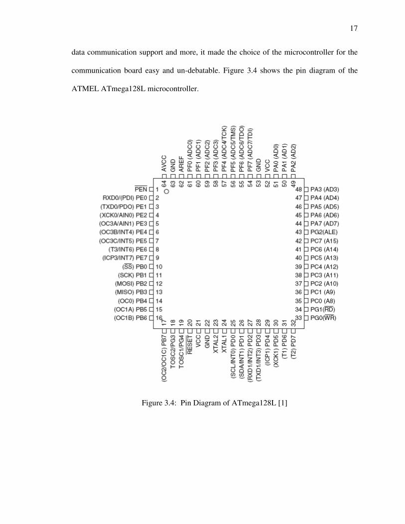
data communication support and more, it made the choice of the microcontroller for the
communication board easy and un-debatable. Figure 3.4 shows the pin diagram of the
ATMEL ATmega128L microcontroller.
Figure 3.4: Pin Diagram of ATmega128L [1]
18
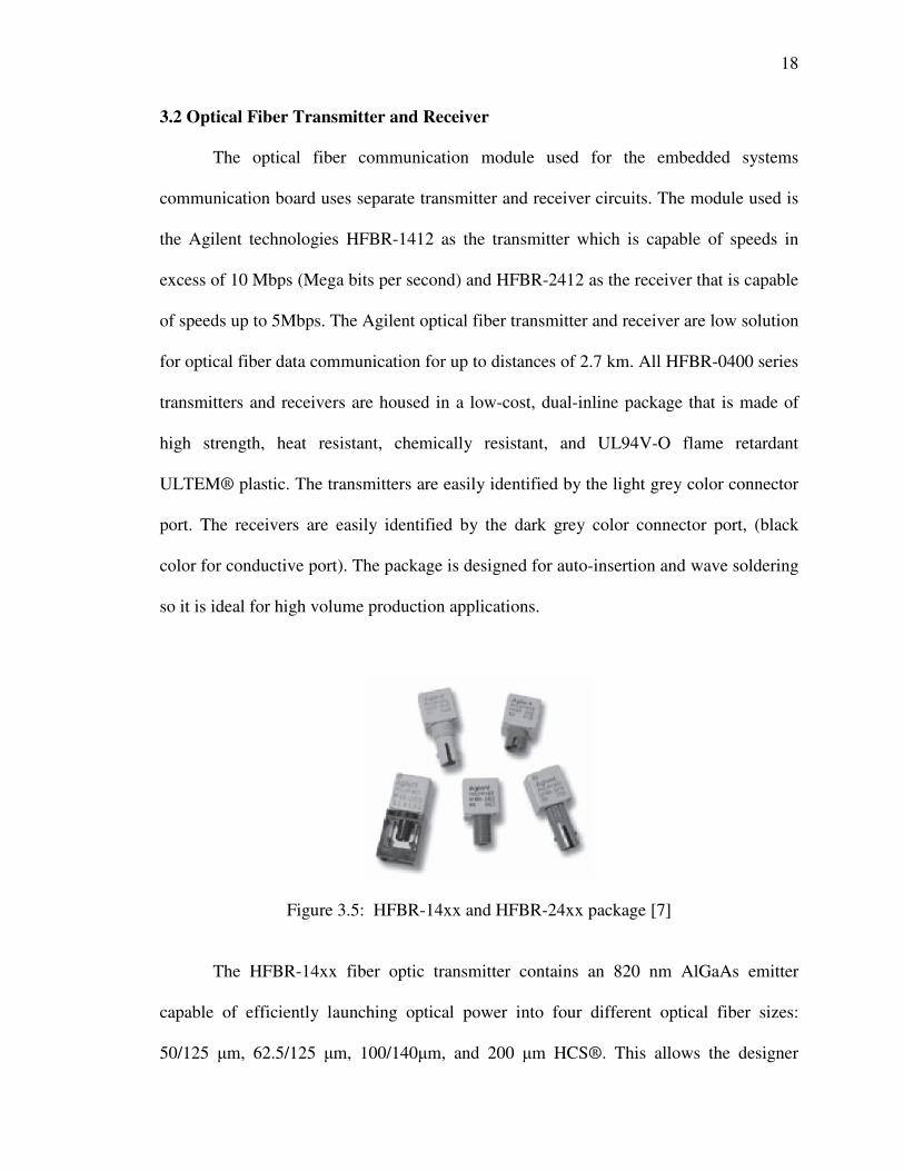
3.2 Optical Fiber Transmitter and Receiver
The optical fiber communication module used for the embedded systems
communication board uses separate transmitter and receiver circuits. The module used is
the Agilent technologies HFBR-1412 as the transmitter which is capable of speeds in
excess of 10 Mbps (Mega bits per second) and HFBR-2412 as the receiver that is capable
of speeds up to 5Mbps. The Agilent optical fiber transmitter and receiver are low solution
for optical fiber data communication for up to distances of 2.7 km. All HFBR-0400 series
transmitters and receivers are housed in a low-cost, dual-inline package that is made of
high strength, heat resistant, chemically resistant, and UL94V-O flame retardant
ULTEM® plastic. The transmitters are easily identified by the light grey color connector
port. The receivers are easily identified by the dark grey color connector port, (black
color for conductive port). The package is designed for auto-insertion and wave soldering
so it is ideal for high volume production applications.
Figure 3.5: HFBR-14xx and HFBR-24xx package [7]
The HFBR-14xx fiber optic transmitter contains an 820 nm AlGaAs emitter
capable of efficiently launching optical power into four different optical fiber sizes:
50/125 µm, 62.5/125 µm, 100/140µm, and 200 µm HCS®. This allows the designer

19
flexibility in choosing the fiber size. The HFBR-14xx is designed to operate with the
Agilent HFBR-24xx fiber optic receivers. The HFBR-14xx transmitter’s high coupling
efficiency allows the emitter to be driven at low current levels resulting in low power
consumption and increased reliability of the transmitter. The HFBR-14x4 high power
transmitter is optimized for small size fiber and typically can launch -15.8 dBm optical
power at 60 mA into 50/125 µm fiber and -12 dBm into 62.5/125 µm fiber. The HFBR-
14x2 standard transmitter typically can launch -12 dBm of optical power at 60 mA into
100/140 µm fiber cable.
Figure 3.6: HFBR 14x 2 Transmitters [7]
It is ideal for large size fiber such as 100/140 µm. The high launched optical power level
is useful for systems where star couplers, taps, or inline connectors create large fixed
losses. Consistent coupling efficiency is assured by the double-lens optical system. Power
coupled into any of the three fiber types varies less than 5 dB from part to part at a given

20
drive current and temperature. Consistent coupling efficiency reduces receiver dynamic
range requirements which allows for longer link lengths.
The HFBR-24x2 fiber optic receiver is designed to operate with the Agilent
HFBR-14xx fiber optic transmitter and 50/125 µm, 62.5/125 µm, 100/ 140µm, and 200
µm HCS® fiber optic cable. Consistent coupling into the receiver is assured by the lensed
optical system. Response does not vary with fiber size ≤0.100 µm. The HFBR-24x 2
receivers incorporates an integrated photo IC containing a photo detector and dc amplifier
driving an open collector schottky output transistor. The HFBR-24x2 is designed for
direct interfacing to popular logic families. The absence of an internal pull-up resistor
allows the open collector output to be used with logic families such as CMOS requiring
voltage excursions much higher than VCC.
Figure 3.7: HFBR 24x2Receiver [7]
Both the open-collector “data” output pin 6 and VCC pin 2 are referenced to “com” pin 3,
7. The “data” output allows busing, strobing and wired “OR” circuit configurations. The
transmitter is designed to operate from a single +5 V supply. It is essential that a bypass
21
capacitor (0.1 mF ceramic) be connected from pin 2 (VCC) to pin 3 (circuit common) of
the receiver.
3.3 Infrared Transceiver
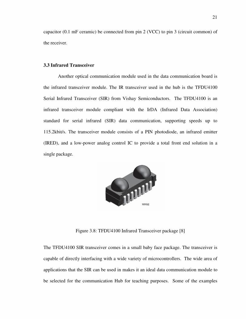
Another optical communication module used in the data communication board is
the infrared transceiver module. The IR transceiver used in the hub is the TFDU4100
Serial Infrared Transceiver (SIR) from Vishay Semiconductors. The TFDU4100 is an
infrared transceiver module compliant with the IrDA (Infrared Data Association)
standard for serial infrared (SIR) data communication, supporting speeds up to
115.2kbit/s. The transceiver module consists of a PIN photodiode, an infrared emitter
(IRED), and a low-power analog control IC to provide a total front end solution in a
single package.
Figure 3.8: TFDU4100 Infrared Transceiver package [8]
The TFDU4100 SIR transceiver comes in a small baby face package. The transceiver is
capable of directly interfacing with a wide variety of microcontrollers. The wide area of
applications that the SIR can be used in makes it an ideal data communication module to
be selected for the communication Hub for teaching purposes. Some of the examples
22
where the TFDU4100 SIR transceiver can be used are printers, fax machines, copiers,
cellular phones, pagers, handhelds, medical and industrial data collecting devices, GPS
and more.
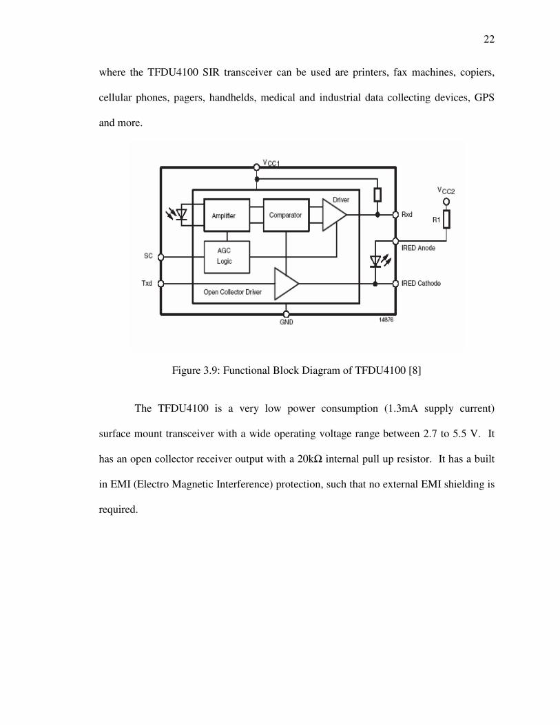
Figure 3.9: Functional Block Diagram of TFDU4100 [8]
The TFDU4100 is a very low power consumption (1.3mA supply current)
surface mount transceiver with a wide operating voltage range between 2.7 to 5.5 V. It
has an open collector receiver output with a 20kΩ internal pull up resistor. It has a built
in EMI (Electro Magnetic Interference) protection, such that no external EMI shielding is
required.

23
TABLE 3.1 Pin description TFDU4100
Pin
Number
Function Description I/O Active
1
IRED
Anode
IRED anode, should be externally connected to VCC2 through a current
control resistor.
2
IRED
Cathode
IRED cathode internally connected to driver transistor.
3
Txd
Transmit Data Input. I HIGH
4 Rxd
Received Data Output, open collector. No external pull-up or pull-down
resistor is required (20 kΩ resistor internal to device). Output data is
invalid during transmission.
O LOW
5
NC
No internal connection.
6
VCC1
Supply Voltage.
7
SC
Sensitivity control. I HIGH
8
GND
Ground.
3.4 Serial RS-232
The RS-232 is a popular serial data communication protocol used to connect the
PC with various data acquisition devices or microcontroller boards. The RS-232 device
can be directly connected to the computer through its communication (COM) port. The
main aim of the RS-232 port to be put on the communication educational board was to
have an option of data communication between the PC and the board. Students working
on the communication board will be able to send and receive data to and from the PC and

24
process it inside the microcontroller. RS which stands for recommended standard was
developed in the 60's by a standards committee now known as the Electronic Industries
Association to develop an interface to connect computer terminals to modems. RS-232
serial communication is a very simple data communication protocol which can be
implemented using both software (if I/O pins of the microcontroller are used) and with
hardware (if UART of the microcontroller is set). In the communication board the RS-
232 port has been connected to the UART pins of the microcontroller. The RS-232
connector was originally developed to use 25 pins called the DB25 connector in which
provisions were made for a secondary serial RS-232 communication channel. In practice,
only one serial communication channel with accompanying handshaking is present. On
personal computers, the smaller DB9 version is more commonly used today.
Figure 3.10: PIN configuration of a DB9 connector for RS-232 port
Figure 3.10 shows a DB9 connector pin out diagram used for RS-232 serial
communication. The RS-232 standard is an asynchronous serial communication in which
the information is sent one bit at a time. Being asynchronous the information is not sent
in a predefined time slots and hence the data transfer can start at any given time. The RS-
232 standard describes a communication protocol where the information or data is sent
bit by bit on a physical channel. The information is broken up in data words. The length
of a data word may vary between 5 and 8 bits typically. For proper transfer additional

25
bits are added for synchronization and error checking or detection purposes. It is
important that the same number of bits be used by the transmitter and the receiver
otherwise the data word may be misinterpreted, or not recognized at all. Each data word
is starts with an attention bit, also known as the start bit. Directly following the start bit,
the data bits are sent. For error detecting purposes, an extra bit is added to the data word
automatically, called the parity bit. The transmitter calculates the value of the bit
depending on the information sent. The receiver performs the same calculation and
checks if the actual parity bit value corresponds to the calculated value. All the data bits
and parity bit are contained in a frame of start and stop bits. The period of time between
the start and stop bit is a constant defined by the baud rate. The start bit always has a
space value (logic 0) and the stop bit always has a marking value (logic 1). If the receiver
detects a value other than marking when the stop bit should be present on the line, it
knows that there is a synchronization failure. This causes a framing error (frames not
received correctly) condition in the receiving UART. The device then tries to
resynchronize on new incoming bits. The signal level of the RS-232 pins can have two
states. A high bit, or marking state is identified by a negative voltage and a low bit or
space state uses a positive value. The voltage limits are shown below.
TABLE 3.2 Voltage limits of RS-232
LEVEL Transmitter capable(V) Receiver capable(V)
Space State(0) +5…..+15 +3….+25
Mark State(1) -5…..-15 -3….-25
Undefined - -3….+3
26
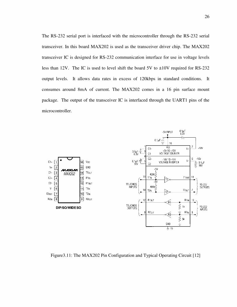
The RS-232 serial port is interfaced with the microcontroller through the RS-232 serial
transceiver. In this board MAX202 is used as the transceiver driver chip. The MAX202
transceiver IC is designed for RS-232 communication interface for use in voltage levels
less than 12V. The IC is used to level shift the board 5V to ±10V required for RS-232
output levels. It allows data rates in excess of 120kbps in standard conditions. It
consumes around 8mA of current. The MAX202 comes in a 16 pin surface mount
package. The output of the transceiver IC is interfaced through the UART1 pins of the
microcontroller.
Figure3.11: The MAX202 Pin Configuration and Typical Operating Circuit [12]

27
The MAX202 consists of three sections; charge-pump voltage converter, drivers
(transmitters) and receivers. The dual charge-pump voltage converter performs the +5V
to ±10V conversion. This section of the IC consists of two voltage converters. The first
converter uses capacitor C1 (shown in figure 3.12) to double +5V to +10V, storing +10V
on the V+ output filter capacitor, C3. The second charge pump voltage converter uses
capacitor C to invert the +10V to -10V, storing the -10V on the V- output filter capacitor,
C4. Figure 3.12 shows the details of the dual charge pump inside the MAX202
transceiver IC.
Figure3.12: Dual Charge pump inside the MAX202 transceiver.[12]
With VCC= 5V the typical driver (transmitter) output voltage swing is ± 8V when loaded
with a normal 5kΩ RS-232 receiver. The output of drivers is inverted. The input
thresholds are both CMOS and TTL compatible. The inputs of the unused drivers can be
left unconnected. When in Low-power shut down mode, the driver outputs are turned off
and their leakage current is less than 1µA. The receivers convert RS-232 signal to CMOS
logic output levels. Receiver outputs are inverting, maintaining compatibility with the
driver outputs.

28
3.4 Serial USB
A Universal Serial Bus or simply USB is one of the most popular and easy to use
data communication ports in use these days. They are available in all PCs and most of
the data acquisition devices, which makes them a good choice to be put on our
communication educational board. USB ports are incredibly easier to use as compared to
other connecting devices to the computer like serial RS-232 or parallel ports. The USB
gives us the flexibility and ease to connect up to 127 devices to the PC. The USB gives
us a maximum data rate of 480Mbits per second. The USB cable consists of two power
lines, ground and +5V and a twisted pair which carries data. In the communication board
the USB port has been interfaced with the microcontroller through the UART pins. The
connection between the PC and the microcontroller UART via the USB takes place
through a FT232BM USB UART IC, used for Asynchronous Serial Data Transfer. The
chip supports 7 or 8 data bits, 1 or 2 stop bits and a parity bit. The chip uses an external 6
MHz crystal oscillator. The FT232BM IC has an integrated level converter to provide an
output voltage of 3.3V. The USB port gives an additional power supply to the
communication board. It provides a regulated 5V supply in addition to the main
regulated power supply from the board’s main power circuit.
The Figure 3.13 shows the functional block diagram of the FT232 BM. The 3.3V
LDO Regulator generates the 3.3 volt reference voltage for driving the USB transceiver
cell output buffers. It requires an external decoupling capacitor to be attached to the
3V3OUT regulator output pin. It also provides 3.3v power to the RSTOUT# pin. The
main function of this block is to power the USB Transceiver and the reset generator cells
rather than to power external logic. However, external circuitry requiring 3.3v nominal at

29
a current of not greater than 5mA could also draw its power from the 3V3OUT pin if
required.
The USB transceiver cell provides the USB 1.1 / USB 2.0 full-speed physical
interface to the USB cable. The output drivers provide 3.3 volt level slew rate control
signaling, whilst a differential receiver and two single ended receivers provide USB data
in, SEO and USB reset condition detection.
Figure3.13: Functional block diagram of FT232BM USB to serial IC [9]
The USB DPLL cell locks on to the incoming NRZI USB data and provides separate
recovered clock and data signals to the SIE block. The 6MHz oscillator cell generates a
6MHz reference clock input to the x8 clock multiplier from an external 6MHz crystal or
ceramic resonator. The x8 clock multiplier takes the 6MHz input from the oscillator cell

30
and generates a 12MHz reference clock for the SIE, USB protocol engine and UART
FIFO controller blocks. It also generates a 48MHz reference clock for the USB DPPL
and the baud rate generator blocks. The Serial Interface Engine (SIE) block performs the
parallel to serial and serial to parallel conversion of the USB data. In accordance to the
USB 1.1 specification, it performs bit stuffing / un-stuffing and CRC5 / CRC16
generation / checking on the USB data stream. Data from the USB data out endpoint is
stored in the dual port TX buffer and removed from the buffer to the UART transmit
register under control of the UART FIFO controller. Data from the UART receive
register is stored in the dual port RX buffer prior to being removed by the SIE on a USB
request for data from the device data in endpoint. The UART FIFO controller handles the
transfer of data between the dual port RX and TX buffers and the UART transmit and
receive registers.
The UART performs asynchronous 7 / 8 bit parallel to serial and serial to parallel
conversion of the data on the RS-232 (RS422 and RS485) interface. Control signals
supported by the UART include RTS, CTS, DSR, DTR, DCD and RI. The UART
provides a transmitter enable control signal (TXDEN) to assist with interfacing to RS485
transceivers. The UART supports RTS/CTS, DSR/DTR and X-On/X-Off handshaking
options. Handshaking, where required, is handled in hardware to ensure fast response
times. The UART also supports the RS-232 break setting and detection conditions. The
baud rate generator provides a x16 clock input to the UART from the 48MHz reference
clock and consists of a 14 bit pre-scalar and 3 register bits which provide fine tuning of
the baud rate (used to divide by a number plus a fraction). This determines the baud rate
of the UART which is programmable from 183 baud to 3 million baud. The reset

31
generator cell provides a reliable power-on reset to the device internal circuitry on power
up. The figure below (figure 3.14) shows the PIN-OUT diagram of the FT232BM IC and
its schematic symbol.
Figure3.14: FT232BM pin out and schematic symbol [9]
An additional RESET# input and RSTOUT# output are provided to allow other devices
to reset the FT232BM or the FT232BM to reset other devices respectively. During reset,
RSTOUT# is high-impedance otherwise it drives out at the 3.3v provided by the onboard
regulator. It can also be used to reset other devices. RSTOUT# will stay high-impedance
for approximately 5ms after VCC has risen above 3.5v and the device oscillator is
running. RESET# should be tied to VCC unless it is a requirement to reset the device
32
from external logic or an external reset generator IC. Though the FT232BM will work
without the optional EEPROM, an external 93C46 ( 93C56 or 93C66 ) EEPROM can be
used to customize the USB VID, PID, serial number, product description strings and
power descriptor value of the FT232BM for OEM applications. The EEPROM is also
required for applications where multiple FT232BM’s are connected to a single PC as the
drivers rely on a unique serial number for each device to bind a unique virtual COM port
to each individual device. The EEPROM should be a 16 bit wide configuration such as a
MicroChip 93LC46B or equivalent capable of a 1Mb/s clock rate at VCC = 4.4v to
5.25v.
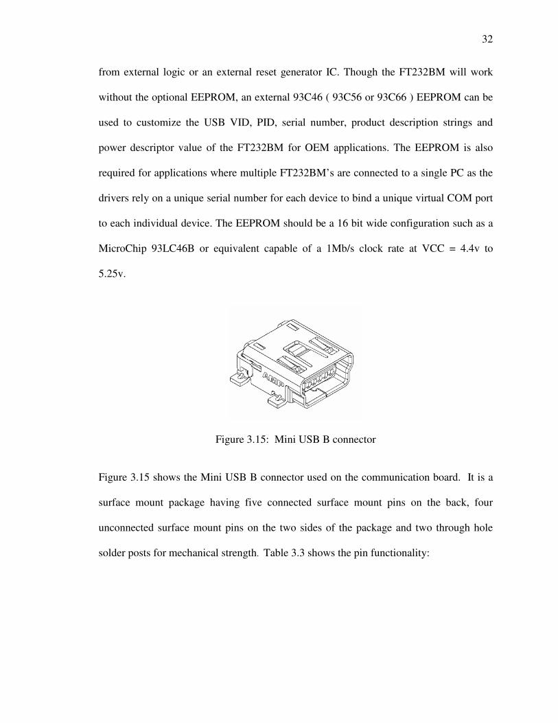
Figure 3.15: Mini USB B connector
Figure 3.15 shows the Mini USB B connector used on the communication board. It is a
surface mount package having five connected surface mount pins on the back, four
unconnected surface mount pins on the two sides of the package and two through hole
solder posts for mechanical strength. Table 3.3 shows the pin functionality:

33
TABLE 3.3: USB Mini B connector Pin functionality
Pin No. Symbol Functionality
1 Vcc +5V Vcc
2 D- Data pin negative
3 D+ Data pin positive
4 Vss/GND Ground pin
5 NC Shield / not connected
3.5 Other Hardware
3.5.1 LCD module
The LCD module used for the board is the ACM0802C, from AZ, Displays, Inc.
It is an 8x2 LCD module (8 characters and 2 lines). The ACM0802C was chosen for the
communication board because of its simplicity of use.
Figure 3.16: ACM0802 LCD Module

34
Table 3.4 shows the pin assignment of the LCD module:
TABLE 3.4 ACM0802 LCD Pin functionality
Pin No. Symbol FUNCTION
1 Vss Ground
2 Vdd +5V
3 Vo LCD contrast adjust
4 RS Register select
5 R/W Read/Write
6 E Enable
7 DB0 Data bit 0
8 DB1 Data bit 1
9 DB2 Data bit 2
10 DB3 Data bit 3
11 DB4 Data bit 4
12 DB5 Data bit 5
13 DB6 Data bit 6
14 DB7 Data bit 7
+/A BL+ Power supply for BL+
-/K BL- Power supply for BL-
3.5.2 Switches and LEDs
Switches and LEDs are provided on the board of debugging purposes. There are four
switches and four LEDs present on the communication board. The switches used are the
small 4mm J hook surface mount switches having a maximum current rating of 100mA.
Figure 3.17 shows the drawing of the switch.
Figure 3.17: 4mm J hook surface mount switch
Apart from the four switches, there are four debugging LEDs present on the board.
These LEDs can be programmed and used along with different transceiver modules to
35
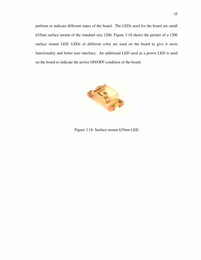
perform or indicate different states of the board. The LEDs used for the board are small
635nm surface mount of the standard size 1206. Figure 3.18 shows the picture of a 1206
surface mount LED. LEDs of different color are used on the board to give it more
functionality and better user interface. An additional LED used as a power LED is used
on the board to indicate the power ON/OFF condition of the board.
Figure 3.18: Surface mount 635nm LED

36
CHAPTER 4: INTERFACING AND SCHEMATIC DESIGN
4.1 Overview of OrCAD Capture
The board schematic has been designed using cadence OrCAD capture® tools.
OrCAD capture® is one of the software tools which forms a part of a large family of
hardware design tools supported by OrCAD, namely OrCAD layout plus, OrCAD AD
design, OrCAD circuit simulator etc. The OrCAD capture can be used to design various
electrical circuits including analog and digital schematics. It further provides built in
features for design verification and processing of the design for manufacture.
The OrCAD capture provides a very simple Windows® user interface for the
designer. It allows the user to organize an entire project in the form of separate design
sheets or windows. Each of these designs are a part of a single project, however for the
ease of the designer and the clarity of the schematic any big project can be split into any
number of pages while maintaining the overall continuity of the design. Separate
schematic pages within a schematic folder are electrically connected and form a part of
the whole design. Ofpage connectors are used to connect wire segments of the same
name in different schematic pages. This allows electrical connectivity between
components which are connected electrically but are present in different schematic pages.
The OrCAD capture project manager forms an important part of any schematic design.
Besides providing an organized view into the contents of the different design files and
schematic pages, it also allows the user to view other related folders like the library
folder, the design cache and the output folder. The library folder contains the information
about component design libraries, the design cache contains an archive of each unique

37
part and symbol used in the design, while the output folder contains files generated
through different auto generation tools namely the bill of materials or the netlist.
The netlist and bill of materials (BOMs) is created by the OrCAD tool by
extracting information contained in the schematic database. The properties of each part or
component can also be extracted in the form of a text file.
One important tool available with the OrCAD capture is the DRC (design rule
check). As the name suggests it detects errors present in the schematic design. An error in
the design may be in the form of a duplicate part, an invalid design packaging,
unconnected or floating signals or wires, electrical design violations etc. The DRC allows
a comprehensive verification of the design before the user moves to the final stage of
generating the netlist (*.mnl) file. The netlist file is used to export the schematic design
into OrCAD layout for the board layout design.
OrCAD tools provide facilities to design a new part or modify an already existing
part from the library. The library holds thousands of different circuit parts which can be
easily dragged and dropped on to the schematic page. Any alteration in the parts can be
made by editing the part and its properties. The components can be easily moved,
dragged, rotated or mirrored individually or as a part of a group using the mouse. The
right click of the mouse over any component or object provides fast access to editing and
properties for that component. Figure 4.1 shows a typical OrCAD schematic capture
window.

38
Figure 4.1: Capture design window
4.2 Microcontroller Circuit
The entire board design is divided into five parts for the ease of the design. The
first part is the microcontroller schematic design. This part of the schematic carries the
ATmega128L microcontroller and the related components. Two I/O connector sockets
each of length 16x2 have been provided on the board for easy I/O interface with the
board. Port A, B, and C are placed on the first I/O connector socket and ports D, E, F and
G have been placed on the second connector socket. A total of 51 I/O pins have been
made available on the board for interfacing

39
Figure 4.2: I/O connector sockets for future hardware interface
Two external crystal oscillators, 32.768 KHz and 8.0 MHz are connected to the
microcontroller through selection jumpers. A 5x2 pin connector for JTAG interface is
connected to the microcontroller for programming.
Figure 4.3: JTAG 10 pin connector schematic

40
Programming of AVR parts via JTAG is performed via the four-pin JTAG port, TCK,
TMS, TDI, and TDO. The JTAG interface is accessed through these four AVR’s pins. In
JTAG terminology, these pins constitute the Test Access Port –– TAP [26] , namely:
• TMS: Test mode select. This pin is used for navigating through the TAP-controller state
machine.
• TCK: Test clock. JTAG operation is synchronous to TCK.
• TDI: Test Data In. Serial input data to be shifted in to the Instruction Register or Data
Register (Scan Chains).
• TDO: Test Data Out. Serial output data from Instruction Register or Data Register.
These are the only pins that need to be controlled or observed to perform JTAG
programming (in addition to power pins). It is not required to apply 12V externally. The
JTAGEN fuse must be programmed and the JTD bit in the MCUCSR. Register must be
cleared to enable the JTAG Test Access Port [26].
4.2 Optical Communication Circuit.
Figure 4.4 is the recommended coupling circuit for the HFBR optical fiber transmitter
and receiver used on the board.
Figure 4.4: Typical Circuit configuration for HFBR 14xx and HFBR 24xx. [7]

41
If resistor R1 in Figure 2 is 70.4 W, a forward current IF of 48 mA is applied to the
HFBR-14x4 LED transmitters. With IF = 48 mA the HFBR-14x4/24x2 logic link is
guaranteed to work with 62.5/125 µm fiber optic cable over the entire range of 0 to 1750
meters at a data rate of up to 5 MBd (Mega baud = Mega bits per second), with arbitrary
data format and pulse width distortion typically less than 25%. By setting R1=115 W, the
transmitter can be driven with IF = 30 mA, if it is desired to economize on power or
achieve lower pulse distortion. It is essential that a bypass capacitor (0.01 µF to 0.1 µF
ceramic) be connected from pin 2 to pin 7 of the receiver. Total lead length between both
ends of the capacitor and the pins should not exceed 20 mm.
The HFBR 1412 optical fiber transmitter is connected to the ATmega128
microcontroller through the UART0_tx pins (Port E 1 pin). In the part of the schematic
shown in Figure 4.5 below the PIN 2 of the driver chip DS7545 is connected to Port E 1
of the microcontroller.
Figure 4.5: Optical fiber transmitter HFBR 1412 schematic

42
Figure 4.6 shows the coupling circuit for the HFBR 2412, optical fiber receiver. The
output of the receiver is connected to the UART0 receive pin at PORT E 0 of the
ATmega128L microcontroller. The output of the receiver is inverted so an inverter chip
SN7404 is used between the microcontroller and the optical fiber receiver. For complete
details of the optical fiber transmitter and receiver schematic circuits, see Appendix A at
the end.
Figure 4.6: Optical fiber Receiver HFBR 2412 schematic
The second part of the optical communication circuit is the Infrared transceiver.
The circuit shown in Figure 4.7 is the recommended schematic circuit for TFDU4100.
The only required components for designing IR transceivers are a current limiting resistor
to the IRED. However, depending on the entire system design and board layout,
additional components may be required. It is recommended that the capacitors C1 and C2
are positioned as near as possible to the transceiver power supply pins. A tantalum

43
capacitor should be used for C1, while a ceramic capacitor should be used for C2 to
suppress RF noise. Also, when connecting the described circuit to the power supply, low
impedance wiring should be used.
Figure 4.7: Recommended circuit for TFDU4100 Transceiver [8]
R1 is used for controlling the current through the IR emitter. For increasing the output
power of the IRED, the value of the resistor should be reduced. Similarly, to reduce the
output power of the IRED, the value of the resistor should be increased. R2, C1 and C2
are optional and dependent on the quality of the supply voltage VCC1 and injected noise.
An unstable power supply with dropping voltage during transmission may reduce
sensitivity (and transmission range) of the transceiver. Figure 4.8 shows the part of the
schematic design for the infrared transceiver.

44
Figure 4.8: TFDU4100 Infra red Transceiver Schematic
4.3 Serial RS-232 Circuit
The third part of the schematic design consists of the RS-232 serial port design.
The DB9 connector used for serial RS-232 communication as discussed in the earlier part
of the paper is interfaced with the microcontroller through the MAX202 IC chip. The
MAX202 transceiver IC is designed for RS-232 communication interface for use in
voltage levels less than 12V. The IC is used to level shift the board 5V to ±10V required
for RS-232 output levels. It allows data rates in excess of 120kbps in standard
conditions. It consumes around 8mA of current. The MAX202 comes in a 16-pin surface
mount package. The output of the transceiver IC is interfaced through the UART1 pins
of the microcontroller.

45
Figure 4.9: The DB9 connector and the serial driver IC MAX202 for serial interface
The RS-232_TD and RS-232_RTS pins of the serial DB9 connector are
connected to the receiver input R1IN and R2IN. The other three receiver inputs are
grounded. The driver outputs T1OUT and T2OUT are connected to the RS-232_RD and
RS-232_CTS pins of the serial DB9 connector. The TXD1 and CTS pins of the
microcontroller are connected to the driver inputs T1IN and T2IN of the MAX202. The
RXD1 an RTS of the microcontroller are connected to the receiver output pins R1OUT
and R2OUT. For detailed schematic see APPENDIX A.
4.4 Serial USB Circuit
The serial USB interface is the last communication module included on the board.
The board used a USB mini B connector as discussed earlier in this document. The USB
mini B connector is interfaced with the ATmega128L microcontroller through the
FT232BM driver IC. Figure 4.10 shows how the USB mini B connector is connected to
the FT232BM IC.

46
Figure 4.10: USB mini B connector interface with FT232BM driver IC
The D+ and D- pins of the USB connector are connected to the PIN 7( USBDP) & and
PIN 8 (USBDM) of the UART USB to serial IC driver chip (FT232BM) through 27 ohm
current limiting resistors. Figure 4.11 illustrates how the FT232BM is used with a 6MHz
crystal or 2-Pin ceramic resonator. In this case, these devices do not have in-built loading
capacitors so these have to be added between XTIN, XTOUT and GND as shown. A
value of 27pF is shown as the capacitor in the Figure 4.11 – this has been recommended
in the data sheet of the FT232BM as the standard value to be used.

47
Figure 4.11: A two pin ceramic crystal configuration with the FT232BM driver IC
Figure 4.12 illustrates how to connect the FT232BM to the 93LC46B (93C56 or 93C66)
EEPROM. EECS (pin 32) is directly connected to the chip select (CS) pin of the
EEPROM. EESK (pin 1) is directly connected to the clock (SK) pin of the EEPROM.
EEDATA (pin 2) is directly connected to the Data IN (DIN) pin of the EEPROM.
Figure 4.12 EEPROM 93C46 configuration with the FT232BM driver IC

48
There is a potential condition whereby both the Data Output (DOUT) of the
EEPROM can drive out at the same time as the EEDATA pin of the FT232BM. To
prevent potential data clash in this situation, the DOUT of the EEPROM is connected to
EEDATA of the FT232BM via a 2.2K resistor. Following a power-on reset or a USB
reset, the FT232BM will scan the EEPROM to find out if an EEPROM is attached to the
Device and if the data in the device is valid. If both of these conditions are true, the
FT232BM will use the data in the EEPROM, otherwise it will use the built-in default
values. When a valid command is issued to the EEPROM from the FT232BM, the
EEPROM will acknowledge the command by pulling the DOUT pin low. In order to
check for this condition, it is necessary to pull DOUT high using a 10k resistor. If the
command acknowledge doesn’t happen then EEDATA will be pulled high by the 10k
resistor during this part of the cycle and the device will detect an invalid command or no
EEPROM present.
4.5 Power Circuit
The power circuit has been designed keeping in mind the voltage ratings and the
different voltage ranges within which all the components present on the board work
reliably. The DC connector can be hooked to a voltage source ranging between 9V to
15V DC. A power slide switch is provided on the board to allow manual control of
power. The power slide switch used on the board is a two way sliding, surface mount six
pin package switch. The voltage coming into the board between 9V to 15V DC needs to
be brought down to an operating range of regulated 5V DC for the board to work.

49
Figure 4.13: Schematic showing the DC jack and the sliding switch
A bridge rectifier circuit followed by a 5V DC regulator has been used for this
purpose. The bridge rectifier is a standard DF10S surface mount IC chip, with high
current and high surge current capabilities. The voltage regulator used is a standard
78M05A, positive regulator. It employs internal current limiting, thermal shutdown and
safe area protection, making it essentially indestructible.
Figure 4.14 Schematic of the rectifier bridge and the 7805 voltage regulator.

50
The 7805 fixed voltage regulators are designed with Thermal Overload Protection [24]
that shuts down the circuit when subjected to an excessive power overload condition,
Internal Short-Circuit Protection that limits the maximum current the circuit will pass,
and Output Transistor Safe-Area Compensation that reduces the output short-circuit as
the voltage across the pass transistor is increased.
Figure 4.15 Block diagram of the 7805 voltage regulator.[24]
4.6 Circuit for On Board LCD Screen
The LCD module used for the board is the ACM0802C, from AZ Displays, Inc.
The LCD module is easy to interface with any microcontroller. The LCD module has 8
data pins that are connected to the I/O pins of Port A of the microcontroller. Only four of
the 8 data pins are connected to the Port A and the rest four are connected to the ground.
The Pin 3 of the LCD module is connected to a 10K potentiometer for providing the LCD
contrast. Pin 7, 8, 9 and 10 of the LCD module have been grounded as seen in the Figure
4.16. These pins represent the lower 4 data bits. The upper 4 data bits have been
connected to the Port A of the microcontroller.

51
Figure 4.16 Schematic showing the LCD module.
4.7 Circuit for debugging LEDs and Switches
Switches and LEDs are provided on the board of debugging purposes. There are
four switches and four LEDs present on the communication board. The switches used are
the small 4mm J hook surface mount switches having a maximum current rating of
100mA. Each of the switches has been connected to a 10K pull up resistors. The LEDs
are connected through a current limiting resistor of 470 ohms. All the LEDs and the
Switches are connected to the port C of the microcontroller and each can be programmed
for a particular user defined function.

52
Figure 4.17 Schematic showing LEDs and Switches.

53
CHAPTER 5: TESTING
5.1 Programming of the Board
. The communication board comes with a JTAG interface for
programming. The ATmega128 AVR is supported with a full suite of program and
system development tools including: C compilers, macro assemblers, program
debugger/simulators, in-circuit emulators, and evaluation kits. The microcontroller is
programmed using AVR Studio4 and IAR Embedded workbench which also supports
most of the AVRs. The AVR Studio® 4 is the professional Integrated Development
Environment (IDE) for writing and debugging AVR® applications in Windows®
9x/NT/2000/XP environments. AVR Studio 4 includes an assembler and a simulator. A
JTAGICE mkII connector is connected between the PC and the board to download code
to the ATmega128L microcontroller through the JTAG connector.
Figure 5.1 The setup to program AVR microcontroller using JTAG ICE
54
Since the testing of the various modules had to be done before the communication
boards goes for manufacturing and further design processing, we had to use different
evaluation boards readily available in the market for different modules for testing with
the ATmega128 microcontroller. The subsequent sections will deal with the testing of the
various modules using different evaluation boards and circuits available readily in the
market. These evaluation boards or test boards have the same circuit and components as
being used on the communication board. Testing the different modules using the
evaluation boards is easier and less time consuming. To duplicate the whole schematic
circuits comprising of hundreds of small components on a bread board and interfacing it
with the ATmega128 microcontroller is not only difficult and time consuming but also
highly susceptible to erroneous results because of possible imperfect and loose
connections and mistakes in arranging the small parts correctly.
5.2 Testing for Microcontroller
The evaluation board used for testing the microcontroller ATmega128 is the STK
500 and the STK 501 daughter board. Figure 5.2 shows the detailed block level diagram
of the STK board. The board comes with the 8 yellow LEDs and 8 push-button switches.
The LEDs and switches are connected to debug headers that are separated from the rest
of the board. They can be connected to the AVR devices with the supplied 10-wire cable
to the pin header of the AVR I/O ports. The STK500 includes two RS-232 ports. One RS-
232 port is used for communicating with AVR Studio. The other RS-232 can be used for
communicating between the target AVR microcontroller in the socket and a PC serial
port connected to the RS-232.
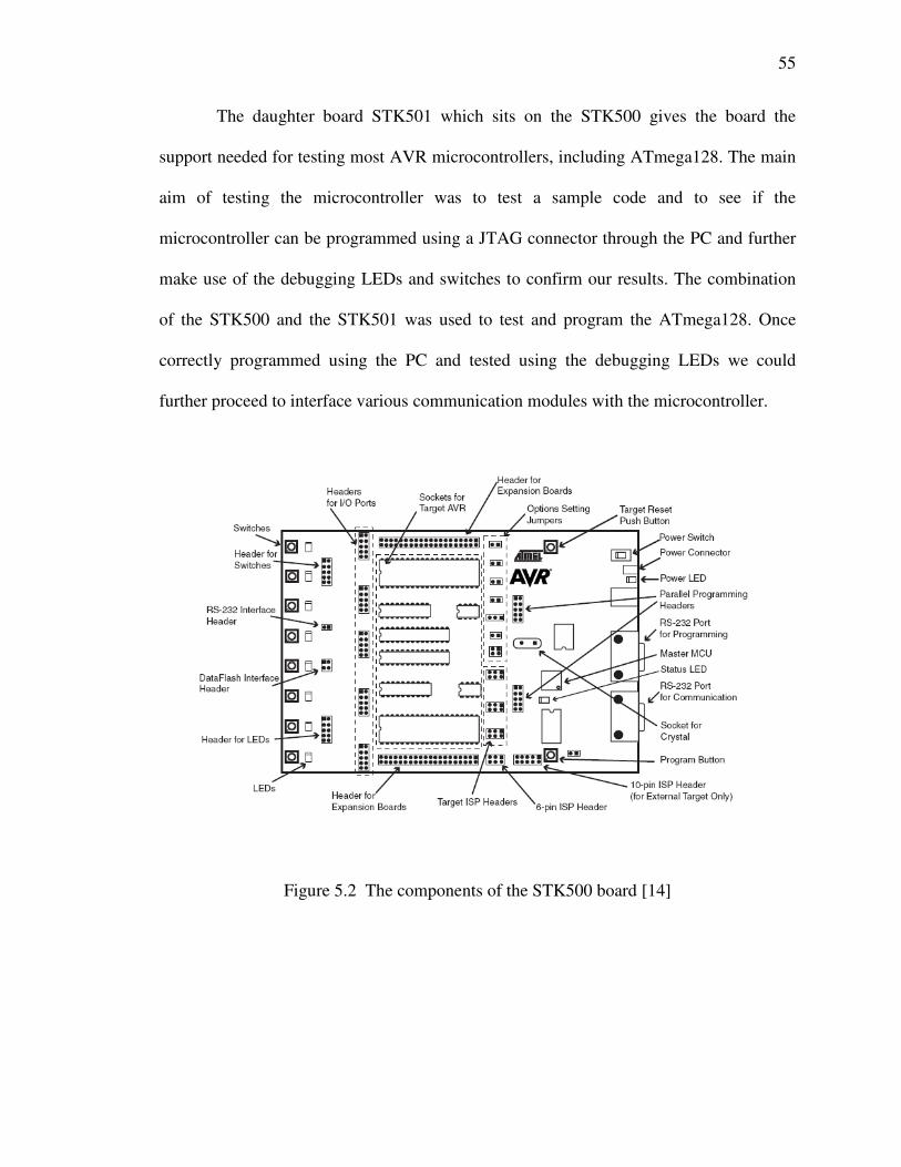
55
The daughter board STK501 which sits on the STK500 gives the board the
support needed for testing most AVR microcontrollers, including ATmega128. The main
aim of testing the microcontroller was to test a sample code and to see if the
microcontroller can be programmed using a JTAG connector through the PC and further
make use of the debugging LEDs and switches to confirm our results. The combination
of the STK500 and the STK501 was used to test and program the ATmega128. Once
correctly programmed using the PC and tested using the debugging LEDs we could
further proceed to interface various communication modules with the microcontroller.
Figure 5.2 The components of the STK500 board [14]
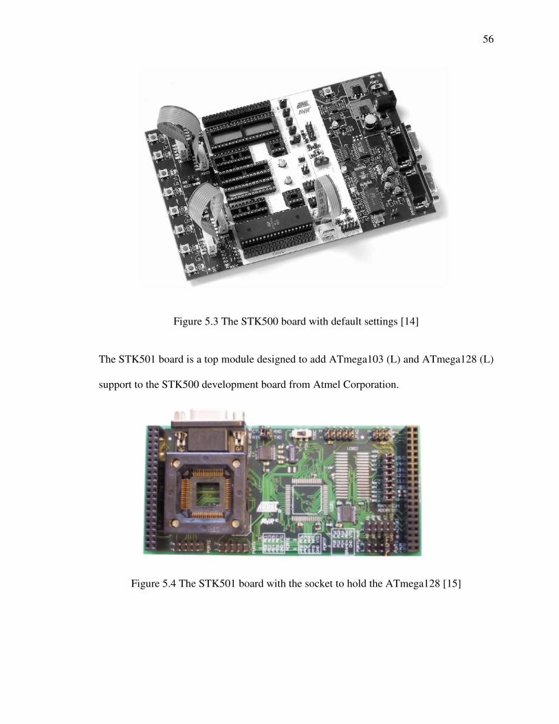
56
Figure 5.3 The STK500 board with default settings [14]
The STK501 board is a top module designed to add ATmega103 (L) and ATmega128 (L)
support to the STK500 development board from Atmel Corporation.
Figure 5.4 The STK501 board with the socket to hold the ATmega128 [15]
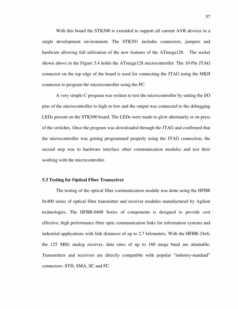
57
With this board the STK500 is extended to support all current AVR devices in a
single development environment. The STK501 includes connectors, jumpers and
hardware allowing full utilization of the new features of the ATmega128. The socket
shown above in the Figure 5.4 holds the ATmega128 microcontroller. The 10-Pin JTAG
connector on the top edge of the board is used for connecting the JTAG using the MKII
connector to program the microcontroller using the PC.
A very simple C program was written to test the microcontroller by setting the I/O
pins of the microcontroller to high or low and the output was connected to the debugging
LEDs present on the STK500 board. The LEDs were made to glow alternately or on press
of the switches. Once the program was downloaded through the JTAG and confirmed that
the microcontroller was getting programmed properly using the JTAG connection, the
second step was to hardware interface other communication modules and test their
working with the microcontroller.
5.3 Testing for Optical Fiber Transceiver
The testing of the optical fiber communication module was done using the HFBR
0x400 series of optical fiber transmitter and receiver modules manufactured by Agilent
technologies. The HFBR-0400 Series of components is designed to provide cost
effective, high performance fiber optic communication links for information systems and
industrial applications with link distances of up to 2.7 kilometers. With the HFBR-24x6,
the 125 MHz analog receiver, data rates of up to 160 mega baud are attainable.
Transmitters and receivers are directly compatible with popular “industry-standard”
connectors: ST®, SMA, SC and FC.
58
These modules are readily available in the market in the form of a testing kit,
which comprises of a HFBR 2412 receiver, a HFBR 1412 transmitter and a 2m long ST
optical fiber cable.
Figure5.5: The Agilent HFBR 04x series Optical Fiber evaluation kit.
The pin diagram and hardware details of the optical fiber transmitter and receiver
have already been discussed in Chapter 3 of this document. The testing of the optical
fiber communication module was done by interfacing the appropriate pins with the
microcontroller UART pins. Two small PCBs were designed to hold the transmitter and
receiver along with the associated coupling circuit on it. Breadboard testing was not used
to avoid lose connections and lose of signal and noise. Well soldered connections were

59
used on the PCB to obtain near perfect testing conditions to duplicate the exact scenario
that would be present in the final optical communication board.
The interfacing part was followed by testing our hardware for its working along
with the microcontroller. This was done by programming the microcontroller UART. A
simple C program was written, which would send bytes regularly on its UART
transmitter pin and the UART receiver pin was programmed to receive these bytes
correctly and make a check if the received byte is received properly without any error.
Due to very less available resources only one microcontroller circuit was used and the
optical fiber was made to echo the bytes back to the microcontroller.
Figure 5.6 Block diagram showing testing of optical fiber module
The main aim of this testing was to identify any anomalies in our circuit design. Our test
results showed that the bytes transmitted through the UART transmitter were able to be
received without any errors at the other end of the optical fiber on the UART receiver
pin.
HFBR Transmitter
Optical Fiber
HFBR Receiver
STK 500-
Microcontroller
Board
UART Tx
UART Rx

60
5.4 Testing for Serial USB
The Serial USB communication module was tested to work with the ATmega128
by using a readily available evaluation kit. The USB2SER kit [25] is a USB to Serial
converter kit manufactured by Parallax. The circuit on the USB2SER board is the same
as used in our USB module for the communication board. This provides us an exact
platform to test our USB circuit without having to create the setup on a breadboard.
Using evaluation boards for testing helps in avoiding any possible errors and variation in
results that could come into picture because of lose connections and larger size of
components used on the breadboard. The USB2SER board provides a very easy way to
connect the PC to the microcontroller.
Figure 5.7: USB to serial converter used for testing the USB circuit.[25]
The USB2SER board bridges the PC’s USB port to the logic level Rx and Tx signals that
can connect directly to a microcontroller’s I/O pins. To the PC it appears as a virtual
COM port and to the microcontroller it appears as a true 3.3V – 5V serial connection
consisting of Rx and Tx signals.

61
The hardware setup for testing the USB circuit consists of connecting the UART
Tx and UART Rx signals with the corresponding connectors of the USB2SER board. The
USB port of the converter is connected to the PC using a USB cable.
A simple UART program was written to test the USB circuit for its working.
Characters where sent out on the UART transmit pin of the microcontroller and received
on the PC using a hyper terminal. Similarly characters where sent from the PC on the
USB to be received on the UART Rx pin of the microcontroller and verified by
displaying on the LCD screen connected on the STK500 board.
This simple exercise of sending and receiving characters from the microcontroller
to the PC and from the PC to the microcontroller gave us the proof of the working of the
USB circuit with the ATmaga128 microcontroller. This test did not measure the speed
and capabilities of the USB circuit involved in our communication board. However it
only tested the working of the circuit on the hardware level, so that it could be approved
for second stage of the design, i.e. board layout design.

62
CHAPTER 6: LAYOUT DESIGN
6.1 Overview
The layout design for the board was done using the ORCAD layout tools. Before
we start work on the board layout a netlist file is created using the ORCAD Capture tools.
The netlist (*.mnl) describes the interconnection of a schematic design using the names
of the nets, components and pins. A netlist contains the following:
• Footprint names
• Electrical packaging
• Component names
• Net names
• The component pin for each net
• Net, pin and component property information.
Following steps are taken to make the board layout using OrCAD layout tools:
1. Ensure that a netlist with all footprints and other necessary information
has been created.
2. Create a directory in which the schematic design, netlist, and board will
coexist and put the schematic design and netlist in it. OrCAD provides a
directory (ORCADWIN\LAYOUT\DESIGN) for this purpose.
3. From the Layout session frame’s File menu, choose New. The Load
Template File dialog box will be displayed.
4. Select a technology template (.TCH), and then choose the Open button.
The Load Netlist Source dialog box will be displayed.

63
5. Select a netlist file (for example, design_name.mnl), then choose the
Open button. The Save File As dialog box displays.
6. Specify a name for the new board (for example, COMM_BOARD.MAX),
then chose the save button. The AutoECO process begins
7. If necessary, respond to the Link Footprint to Component dialog box.
Most of the components used in the communication board did not have footprints
in the ORCAD standard library. All the footprints were made manually using the data
sheet drawings and dimensional details of each component and saved in the ORCAD
library before proceeding further with the LAYOUT design.
6.2 Design of New Footprints
Majority of the components used on the communication board are surface mount
and very small in size. Creating new footprints for these components becomes even more
challenging and difficult. Care must be taken to be as precise as possible, because even a
fraction of an inch error in creating the footprint may cause problems while soldering the
components on the board. Most of the footprints were designed using already present
footprints in the library and modifying them according to the requirements and datasheet
values.
The newly created footprints where then saved in the libraries and the name of the
footprints updated in the schematic design under the property of each component. Note
that the layout design will not be complete unless each component in the schematic
capture design has a specific footprint present in the layout library. Care was taken to
accurately update the properties of each component with their corresponding footprint

64
names in the layout library. When the netlist file (*.mnl) is created in the schematic , it
holds the information about the footprints and other properties of the components and
when we link the netlist in the OrCAD layout, the tools automatically picks up the
corresponding footprint from the libraries to generate the initial board layout design.
Figure 6.1 OrCAD Layout foot print: RS-232 Serial Port
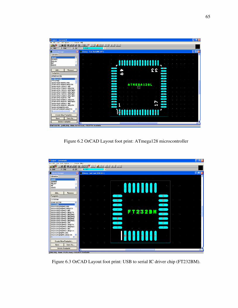
65
Figure 6.2 OrCAD Layout foot print: ATmega128 microcontroller
Figure 6.3 OrCAD Layout foot print: USB to serial IC driver chip (FT232BM).

66
Figure 6.4 OrCAD Layout foot print: 2 Pin Crystal Oscillator
Figure 6.5 OrCAD Layout foot print: 4 Pin crystal oscillator.
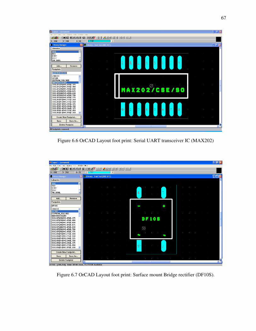
67
Figure 6.6 OrCAD Layout foot print: Serial UART transceiver IC (MAX202)
Figure 6.7 OrCAD Layout foot print: Surface mount Bridge rectifier (DF10S).

68
Figure6.8 OrCAD Layout foot print: USB mini B port
Once all the footprints were created and saved in the library files, the schematic
design was updated with the footprint information for each component. This can be done
by opening the properties window of each component and updating the field “footprints”
with the name and path of the footprint created in OrCAD layout. The second step would
be to create a netlist file in the schematic capture. This netlist file is used as a resource to
create the layout design using the OrCAD tools. The netlist (*.mnl) file is used to export
the schematic design to OrCAD layout tool.

69
CHAPTER 7: CONCLUSION AND FUTURE WORK
The main purpose of this thesis was to design and test a low cost communication
board which is capable of handling different kinds of communication protocols to serve
as a learning tool for students and researchers. Initial effort went into an extensive
research for finding similar communication boards used for educational purposes.
However the result of the research was that there were very few or no boards which could
serve the purpose of including all types of communication modules into one board and
serve as platform for students and researchers to work on. The design and testing of this
communication board has been done in order to manufacture a simple, low cost, small in
size, easy to handle and versatile microcontroller board which holds various
communication modules capable of communicating with another similar board or with a
PC or act as a link between two PCs. Students and researchers will find this board very
useful to learn basic embedded systems and communication theories by conducting lab
exercises and other experiments.
Although a lot of effort and time has gone into the design of the board and then
further testing of the hardware, the board is still in a stage where future work needs to be
done. Major effort was made in the initial design of the board, including the selection of
hardware and other design related components. The effort towards this thesis can be
summarized as follows:
• Initial research for communication boards available in the market.

70
• Research on various communication modules and their working( optical fiber,
infrared, USB, serial UART)
• Preparing lab exercises for the students to work on to ensure that the
communication modules are helpful as a learning tool for embedded systems
students
• Initial research on available hardware for different communication modules.
• Selection of the ideal microcontroller for the board.
• Schematic design for the board.
• Writing test code and driver software for different communication modules.
• Testing of the hardware with different evaluation boards to check the correctness
of our design
• Making design changes to the schematic based on the test results
• Creating foot prints of the components for layout design.
The communication board design was completed and further testing was done
using each communication module to ensure that the manufactured version of the
board will be workable.
The future work in this thesis may include the manufacture of the board and
performing direct tests on the communication modules on the board. Data rates and
limit to which the data rate can be pushed for normal working of the board can be
done. Students taking up embedded systems and advanced embedded systems should
be strongly encouraged to take this up as a project to test the working model of the
embedded communication board. Sample lab exercises have been provided in the
Appendix D of this document. It will serve as a base for students to work on the

71
different data communication modules and test the data rates using serial UART and
I/O pins. Measurement of error rates at different speeds can be carried out.
The communication board has attracted interest in a few of its early
demonstrations, like the one at the annual optical communication conference held in
the University of North Carolina at Charlotte in November, 2005. Faculty members of
different institutions have shown interest in including this board as a part of the
course work in embedded systems and communication classes. The board can serve
as a lab exercise and a practical learning tool for students learning embedded systems
programming and embedded systems communication.

72
REFERENCES
[1] Atmel’s ATmega128L AVR microcontroller.
Website: http://www.atmel.com/dyn/resources/prod_documents/doc2467.pdf
[2] OrCAD Capture
Website: http://www.orcad.com/orcadcapture.aspx
[3] OrCAD Layout
Website: http://www.orcad.com/orcadlayout.aspx
[4] Self Programming AVR
Website: http://www.atmel.com/dyn/resources/prod_documents/doc1644.pdf
[5] I. Vakil and J. M. Conrad, “Design of a Data Communication Hub for use in
Research And Education”, IEEE, SoutheastCon, Memphis, Tennessee, March
2006
[6] J. M. Conrad, S. Lasassmeh, I. Vakil and B. Levine, “Teaching Optical
Communications concepts in Embedded Systems Courses”, Proceedings of the
Frontiers in Education Conference, Indianapolis, IN, October 2005
[7] HFBR 0400: http://www.home.agilent.com/semiconductors
[8] TFDU4100: http://www.vishay.com/docs/82514/82514.pdf
[9] FT232BM: http://www.ftdichip.com/Documents/DataSheets/ds232b18.pdf
[10] I.Vakil and J. M. Conrad, “Embedded Systems Communication Board for
Education and Research”, ICEE, International Conference on Engineering
Education, San Juan, Puerto Rico. July 2006.
[11] J.M. Conrad and I. Howitt, “Introducing Students to Communications Concepts
Using Optical and Low-Power Wireless Devices,” Proceedings of the 2004
International Conference on Engineering Education, Gainesville, FL, October
2004.
[12] MAX202: http://datasheets.maxim-ic.com/en/ds/MAX200-MAX213.pdf
[13] JTAGICE mkII: AVR
http://www.atmel.com/dyn/resources/prod_documents/doc2562.pdf
http://www.msc-ge.com/download/atmel/pdf_avr/JTAGICE_MK2.pdf
[14] STK500: ATMEL
http://www.atmel.com/dyn/resources/prod_documents/doc1939.pdf

73
http://www.atmel.com/dyn/resources/prod_documents/doc1925.pdf
[15] STK501: http://www.atmel.com/dyn/resources/prod_documents/DOC2491.PDF
[16] B. Kamali, “Development of an undergraduate structured laboratory to support
classical and new base technology experiments in communications,” IEEE
Transactions on Education, v 37, n 1, Feb, 1994, pp. 97-105.
[17] B. Kamali, “A Three-Level Structured Laboratory to Support Traditional and
New-Base Technology Experiments in Communications,” NSF Award No.
9153146, University of Texas at San Antonio, May 15 1991 to Oct 31 1993.
[18] L. Sevgi, “EMC and BEM engineering education: Physicsbased modeling, hands-
on training and challenges,” IEEE Antennas and Propagation Magazine, v 45, n 2,
April,2003, p 114-119.
[19] V.E DeBrunner, L.S. DeBrunner, S. Radhakrishnan, Khan Kamal, “The
elecomputing laboratory: A multipurpose laboratory,” IEEE Transactions on
Education, v 44, n 4, November 2001, pp. 302-310.
[20] M. Munoz and S. Garrod, “In process development of an advanced undergraduate
communications laboratory,”Proceedings of the 1997 Frontiers in Education
Conference, v2, 1997. Part 2 (of 3), Nov 5-8 1997.
[21] A. Behagi, “Development of a wireless and satellite communication laboratory at
Penn State Harrisburg,” Proceedings of the 1997 ASEE Annual Conference, Jun
15-18 1997, Milwaukee, WI, USA, 5p.
[22] E. Bertran, F. Tarres and G. Montoro, “Experimental course on digital
communications,” Proceedings of the IEEE International Conference on
Electronics, Circuits, and Systems, v 3, Sep 7-Sep 10 1998, p 321-324.
[23] W.D. Lane, “Textbook principles to communications hardware: Making it work,”
Proceedings of the 1996 Frontiers in Education Conference, v 3, Nov 6-9 1996,
p1504-1507.
[24] ST microelectronics: 78M05A precision regulator.
http://www.st.com/stonline/products/literature/ds/2147.pdf
[25] USB2SER: Parallax:
http://www.parallax.com/dl/docs/prod/acc/USB2SER-v1.1.pdf
[26] JTAG interface “IEEE Std. 1149.1-1993, IEEE Standard Test Port and Boundary
Scan Architecture”, IEEE, Inc., New York.

APPENDIX A: SCHEMATIC
SCHEMATIC: MICROCONTROLLER, JTAG AND I/O PORTS
75
SCHEMATIC: OPTICAL FIBER TRANSMITTER- RECIEVER AND
INFRARED TRANSCIEVER

76
SCHEMATIC: POWER SUPPLY
77
SCHEMATIC: RS-232 PORT AND LCD

78
SCHEMATIC: USB CONNECTOR INTERFACE

79
APPENDIX B: BILL OF MATERIALS (BOM)
Item Quantity Reference Part PCB footprint
_________________________________________________________________________________________
1 1 X1 8Mhz SM/CRYSTAL_2PIN
2 1 CN1 CN-USB DINC/MINI_USB
3 11 C1 100nF SM/C_0603
C2 100nF SM/C_0603
C3 100nF SM/C_0603
C4 100nF SM/C_0603
C5 100nF SM/C_0603
C8 100nF SM/C_0603
C9 100nF SM/C_0603
C12 100nF SM/C_0603
C17 100nF SM/C_0603
C18 100nF SM/C_0603
C28 100nF SM/C_0603
4 2 C7 22pF SM/C_0603
C6 22pF SM/C_0603
5 1 C10 100 nF SM/C_0603
6 3 C11 0.1uF SM/C_0603
C26 0.1uF SM/C_0603
C27 0.1uF SM/C_0603
7 1 C13 10uF/ 16 V SM/C_D55
8 1 C14 0.1 uF SM/C_0603
9 1 C15 10 nF SM/C_0603
10 2 C16 10uF/16V SM/C_D55
C19 10uF/16V SM/C_D55
11 1 D3 RX_LED SM/LED_1206
12 1 D4 TX_LED SM/LED_1206
13 5 D5 LED SM/LED_1206
D6 LED SM/LED_1206
D7 LED SM/LED_1206
D8 LED SM/LED_1206
D9 LED SM/LED_1206
14 1 IC1 ATmega128L ATMEGA128L
15 1 IC2 MAX202/SO MAX202/CSE/SO
16 1 IC3 FT232BM FT232BM
17 1 IC4 93LC46B EEPROM_93LC46B
18 1 IC5 74HC14 74HC14
19 1 IC6 DF10S/SM DF10S

80
20 1 IC7 7805 7805_D2PAK
21 1 J1 JTAG BLKCON.100/JTAG
22 7 J2 JUMPER BLKCON.100/JUMPER
J9 JUMPER BLKCON.100/JUMPER
J10 JUMPER BLKCON.100/JUMPER
J11 JUMPER BLKCON.100/JUMPER
J12 JUMPER BLKCON.100/JUMPER
J14 JUMPER BLKCON.100/JUMPER
J15 JUMPER BLKCON.100/JUMPER
23 1 J3 HFBR_1412_TX HFBR_X412
24 1 J4 HFBR_2412_RX HFBR_X412
25 2 J17 CONN SOCKET 16x2 BLKCON.100/CONN_32
J8 CONN SOCKET 16x2 BLKCON.100/CONN_32
26 1 J13 DC_JACK_2_IMM DC_JACK
27 1 LCD1 LCD MODULE BLKCON.100/LCD
28 1 L1 100mH SM/L_0603
29 1 P1 CONNECTOR DB9 DB9/RS-232
30 9 R1 470 SM/R_0603
R2 470 SM/R_0603
R3 470 SM/R_0603
R4 470 SM/R_0603
R5 470 SM/R_0603
R6 470 SM/R_0603
R22 470 SM/R_0603
R23 470 SM/R_0603
R24 470 SM/R_0603
31 9 R7 10K SM/R_0603
R8 10K SM/R_0603
R9 10K SM/R_0603
R13 10K SM/R_0603
R14 10K SM/R_0603
R18 10K SM/R_0603
R21 10K SM/R_0603
R38 10K SM/R_0603
R39 10K SM/R_0603
32 2 R10 100 SM/R_0603
R41 100 SM/R_0603
33 1 R11 47K SM/R_0603
34 1 R12 10K BLKCON.100/POTENTIOMETERSM/R_0603
35 2 R15 27R SM/R_0603
R16 27R SM/R_0603
81
36 1 R17 4K7 SM/R_0603
37 1 R19 1K5 SM/R_0603
38 1 R20 2K2 SM/R_0603
39 1 R35 14 SM/R_0603
40 1 R36 47 SM/R_0603
41 1 R37 47K SM/R_0603
42 1 R40 1000 SM/R_0603
43 1 R42 500 SM/R_0603
44 5 SW_1 SW PUSHBUTTON-SPST-2/SM SMD_SW
SW_2 SW PUSHBUTTON-SPST-2/SM SMD_SW
SW_3 SW PUSHBUTTON-SPST-2/SM SMD_SW
SW_4 SW PUSHBUTTON-SPST-2/SM SMD_SW
SW_6 SW PUSHBUTTON-SPST-2/SM SMD_SW
45 2 SW_5 SW SLIDE SLIDE_SW
SW1 SW SLIDE SLIDE_SW
46 1 TR1 TFDU4100 TFDU4100
47 1 U13 DS75451/SO SOG.050/8/DS7545_DRIVER
48 1 U16 SN7404 SOG.050/SN7404_INVT
49 1 X3 6Mhz SM/CRYSTAL_2PIN
50 1 Y1 32,768 KHz SM/CRYSTAL_4PIN

82
APPENDIX C: TEST CODE
LCD.h
/*********************************************************/ /* Purpose: LCD Driver */ /* Version: 1 */ /* Author: ISHFAN VAKIL */ /* Date: */ /* www: */ /* email: [email protected] */ /* Software: AVR studio/ IAR */ /* Hardware: STK 500/STK 502 */ /*********************************************************/ #include <ioavr.h> #include <intrinsics.h> #define LOW 0 #define HIGH 1 #define CLS 0x01 #define HOME 0x02 #define ENTRY 0x04 #define INCREMENT 0x02 #define DECREMENT 0x00 #define CONTROL 0x08 #define DISPLAY_ON 0x04 #define DISPLAY_OFF 0x00 #define CURSOR_ON 0x02 #define CURSOR_OFF 0x00 #define BLINK 0x01 #define NO_BLINK 0x00 #define SHIFT 0x10 #define SHI_LEFT 0x00 #define SHI_RIGHT 0x04 #define DIS_LEFT 0x08 #define DIS_RIGHT 0x0C #define FUNCTION_SET 0x20 #define _8BIT 0x10 #define _4BIT 0x00 #define _2LINE 0x08 #define _1LINE 0x00 #define _10DOT 0x04 #define _7DOT 0x00 #define R_W 0x01 #define E 0x04 unsigned char RS; void itoa(unsigned int value, unsigned char * s); void wait(unsigned int duration); void clrscr(void); void home(void); void second_row(void); void first_row(void); void lcd_init(unsigned char line, unsigned char dots); void lcd_out(char c); void put_lcd(const unsigned char * s); void put_lcd_xy(unsigned short int x, unsigned short int y, const unsigned char * s);

83
void itoa(unsigned int value, unsigned char * s) unsigned int i; for (i=4;i>0;i--) s[i] = (value % 10) + 0x30; value /= 10; void wait(unsigned int time) while (time > 0) time--; void clrscr(void) RS = LOW; lcd_out(CLS); wait(1600); lcd_out(HOME); wait(1600); RS = HIGH; void home(void) RS = LOW; lcd_out(HOME); wait(1600); RS = HIGH; void second_row(void) RS = LOW; lcd_out(0x80 | 0x40); wait(1600); RS = HIGH; void first_row(void) RS = LOW; lcd_out(0x80 | 0x00); wait(1600); RS = HIGH; void lcd_init(unsigned char line, unsigned char dots) wait(15000); PORTA = 0x30; PORTA = (0x30 | E); PORTA = 0x30; wait(1000); PORTA = 0x30; PORTA = (0x30 | E);

84
PORTA = 0x30; wait(1000); PORTA = 0x30; PORTA = (0x30 | E); PORTA = 0x30; wait(1000); PORTA = 0x20; PORTA = (0x20 | E); PORTA = 0x20; wait(1000); RS = LOW; lcd_out(FUNCTION_SET | _4BIT | line | dots); lcd_out(CONTROL | DISPLAY_OFF); lcd_out(CONTROL | DISPLAY_ON | CURSOR_OFF | NO_BLINK); lcd_out(CLS); wait(10000); lcd_out(HOME); wait(10000); lcd_out(ENTRY | INCREMENT); RS = HIGH; void lcd_out(char c) PORTA = ((c & 0xF0) | RS); wait(1600); PORTA = ((c & 0xF0) | RS | E); wait(1600); PORTA = ((c & 0xF0) | RS); wait(1600); PORTA = (((c & 0x0F) << 4) | RS); wait(1600); PORTA = (((c & 0x0F) << 4) | RS | E); wait(1600); PORTA = (((c & 0x0F) << 4) | RS); wait(1600); void put_lcd(const unsigned char * s) unsigned short int i; i = 0; do if (s[i] == '\0') break; if (i == 16) second_row(); if (i == 32) first_row(); i = 0; switch (s[i]) case 0xE4: lcd_out(0xE1);

85
break; case 0xF6: lcd_out(0xEF); break; case 0xFC: lcd_out(0xF5); break; default: lcd_out(s[i]); break; i++; wait(1600); while (s[i] != '\0'); void put_lcd_xy(unsigned short int x, unsigned short int y, const unsigned char * s) unsigned short int i,z,help; i = 0; if (y < 4) z = y; else z = 0; switch (z) case 0: help = x; break; case 1: help = x + 0x40; break; case 2: help = x + 0x10; break; case 3: help = x + 0x50; break; default: break; RS = LOW; lcd_out(0x80 | help); wait(1600); RS = HIGH; do if (s[i] == '\0') break; if ((x == 16) && (y == 0)) second_row(); x = 0; y = 1; if ((x == 16) && (y == 3))
86
first_row(); x = 0; y = 0; switch (s[i]) case 0xE4: lcd_out(0xE1); break; case 0xF6: lcd_out(0xEF); break; case 0xFC: lcd_out(0xF5); break; default: lcd_out(s[i]); break; i++; x++; wait(1600); while (s[i] != '\0'); int main( void ) unsigned int i; unsigned char str[8]; i = 0; str[5] = 0; DDRA = 0xFF; DDRB = 0xFF; PORTB = 0xAA; lcd_init(_2LINE,_7DOT); clrscr(); home(); //put_lcd_xy(0,0,"*ISHFAN*"); //put_lcd_xy(0,1,"*VAKIL*"); lcd_out('I'); for (;;) i++; itoa(i,str); put_lcd_xy(6,3,&str[1]); if (i == 9999) i = 0;
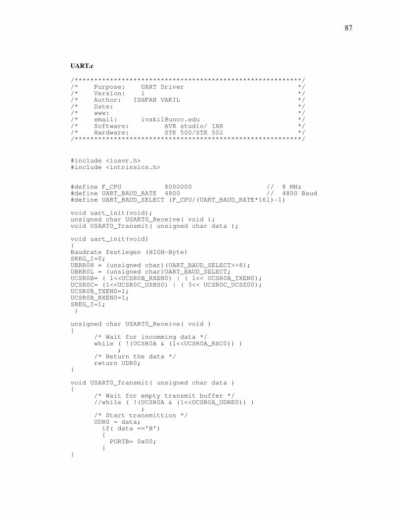
87
UART.c
/**********************************************************/ /* Purpose: UART Driver */ /* Version: 1 */ /* Author: ISHFAN VAKIL */ /* Date: */ /* www: */ /* email: [email protected] */ /* Software: AVR studio/ IAR */ /* Hardware: STK 500/STK 502 */ /**********************************************************/
#include <ioavr.h> #include <intrinsics.h> #define F_CPU 8000000 // 8 MHz #define UART_BAUD_RATE 4800 // 4800 Baud #define UART_BAUD_SELECT (F_CPU/(UART_BAUD_RATE*16l)-1) void uart_init(void); unsigned char USART0_Receive( void ); void USART0_Transmit( unsigned char data ); void uart_init(void) Baudrate festlegen (HIGH-Byte) SREG_I=0; UBRR0H = (unsigned char)(UART_BAUD_SELECT>>8); UBRR0L = (unsigned char)UART_BAUD_SELECT; UCSR0B= ( 1<<UCSR0B_RXEN0) | ( 1<< UCSR0B_TXEN0); UCSR0C= (1<<UCSR0C_USBS0) | ( 3<< UCSR0C_UCSZ00); UCSR0B_TXEN0=1; UCSR0B_RXEN0=1; SREG_I=1; unsigned char USART0_Receive( void ) /* Wait for incomming data */ while ( !(UCSR0A & (1<<UCSR0A_RXC0)) ) ; /* Return the data */ return UDR0; void USART0_Transmit( unsigned char data ) /* Wait for empty transmit buffer */ //while ( !(UCSR0A & (1<<UCSR0A_UDRE0)) ) ; /* Start transmittion */ UDR0 = data; if( data =='B') PORTB= 0x00;

88
void main(void) DDRB=0xFF; PORTB=0xAA; // SREG_I=1; UCSR0B_TXEN0=1; UCSR0B_RXEN0=1; uart_init(); __enable_interrupt(); //sei(); for(;;) /* Forever */ USART0_Transmit('A'); PORTB=0xAA; //UDR0='C'; // PORTE='C';

89
APPENDIX D: SAMPLE LAB EXERCISES
SAMPLE LAB EXERCISE 1:
Learning Objectives: This lab will introduce the students to use UART and interrupts
with optical fiber communication on the communications educational board, along with C
programming concepts to program the ATmega128L.
Laboratory Assignment: In this lab the student will be program the board to transmit
data from one communication board to another using the optical fiber module present on
the board. UART will be used to send and receive data. Error counts will be measured at
different baud rates.
Steps:
1. Create a new project and name it lab_01.
2. Create the main.c file and include appropriate header files.
3. Program the board to meet the requirements ( see requirements).
4. Compile and solve each requirement one at a time.
5. Continue to build and test the code until all the requirements are met.
6. Once all requirements are met, ensure everything is working correctly.
7. Collect the data necessary and write a complete lab report.
Requirements:
1. The code is written in C for the communication board.
2. The code is commented and easy to follow.
3. Use two communication boards to meet the requirements.
4. Connect the optical fiber (provided with the kit) between the optical fiber
transmitter of board 1 and optical fiber receiver of board 2.

90
5. When Switch 1 is pressed on the board 1 start generating characters from ‘a’ to
‘Z’ and continue till Switch 1 is pressed again.
6. Send the characters to the optical fiber transmitter on board 1 by connecting the
UART to Optical fiber jumper on the board.
7. Use queues and interrupts to handle the UART serial communication.
8. On board 2 connect the jumper to connect the UART circuit with the optical fiber
receiver circuit.
9. Use interrupts on board 2 to detect the incoming characters from board 1.
10. On board 2 confirm that the characters received are correct and calculate the error
count.
11. Change the baud rate in both the boards and recompile the program and take error
count measurements again.
12. On the LCD display of board 1 display the character send and the baud rate used
13. On the LCD display of board 2 display the character received and the error count.
14. Take measurements for at least 5 different baud rates and provide the results in a
tabulated form.

91
SAMPLE LAB EXERCISE 2:
Learning Objectives: This lab will introduce the students to use I/O pins and interrupts
with optical fiber communication on the communications educational board, along with C
programming concepts to program the ATmega128L.
Laboratory Assignment: In this lab the student will be program the board to transmit
data from one communication board to another using the optical fiber module present on
the board. I/O pins will be used to send and receive data. Error counts will be measured at
different speeds
Steps:
1. Create a new project and name it lab_02.
2. Create the main.c file and include appropriate header files.
3. Program the board to meet the requirements (see requirements).
4. Compile and solve each requirement one at a time.
5. Continue to build and test the code until all the requirements are met.
6. Once all requirements are met, ensure everything is working correctly.
7. Collect the data necessary and write a complete lab report.
Requirements:
1. The code is written in C for the communication board.
2. The code is commented and easy to follow.
3. Use two communication boards to meet the requirements.
4. Connect the optical fiber (provided with the kit) between the optical fiber
transmitter of board 1 and optical fiber receiver of board 2.

92
5. When switch 1 is pressed on the board 1 start generating characters from ‘a’ to
‘Z’ and continue till switch 1 is pressed again.
6. Program the I/O pin available on the board for serial communication.
7. Program the timers to control the speed of communication.
8. Send the characters to the optical fiber transmitter on board 1 by connecting the
I/O pin from the programmed I/O pin connector to optical fiber jumper on the
board.
9. Receive the characters from the optical fiber receiver on board 2 by connecting
the programmed I/O pin from the I/O pin connector to optical fiber jumper on the
board.
10. On board 2 confirm that the characters received are correct and calculate the error
count.
11. Change the speed by changing the timer interrupt settings and recompile the
program and take error count measurements again.
12. On the LCD display of board 1 display the number of characters sent per second.
13. On the LCD display of board 2 display the number of character received per
second and the error count.
14. Take measurements for at least 5 different speeds and provide the results in a
tabulated form.
15. Measure the highest rate possible at which the error count is 0.

93
SAMPLE LAB EXERCISE 3:
Learning Objectives: This lab will introduce the students to use UART and interrupts
with infrared communication on the communications educational board, along with C
programming concepts to program the ATmega128L.
Laboratory Assignment: In this lab the student will be program the board to transmit
data from one communication board to another using the wireless infrared module
present on the board. UART will be used to send and receive data. Error counts will be
measured at different baud rates and distances between the two boards.
Steps:
1. Create a new project and name it lab_03.
2. Create the main.c file and include appropriate header files.
3. Program the board to meet the requirements (see requirements).
4. Compile and solve each requirement one at a time.
5. Continue to build and test the code until all the requirements are met.
6. Once all requirements are met, ensure everything is working correctly.
7. Collect the data necessary and write a complete lab report.
Requirements:
1. The code is written in C for the communication board.
2. The code is commented and easy to follow.
3. Use two communication boards to meet the requirements.
4. When switch 1 is pressed on the board 1 start generating characters from ‘a’ to
‘Z’ and continue till switch 1 is pressed again.

94
5. Send the characters to the infrared transceiver on board 1 by connecting the
UART to infrared jumper on the board.
6. Use queues and interrupts to handle the UART serial communication.
7. On board 2 connect the jumper to connect the UART circuit with the infrared
transceiver circuit.
8. Use interrupts on board 2 to detect the incoming characters from board 1.
9. On board 2 confirm that the characters received are correct and calculate the error
count.
10. Change the baud rate in both the boards and recompile the program and take error
count measurements again.
11. On the LCD display of board 1 display the baud rate used
12. On the LCD display of board 2 display the character received and the error count.
13. Take measurements for at least 5 different baud rates and provide the results in a
tabulated form.
14. For each baud rate, measure the maximum distance between the two boards for
error free data communication.

95
SAMPLE LAB EXERCISE 4:
Learning Objectives: This lab will introduce the students to use I/O pins and interrupts
with infrared communication on the communications educational board, along with C
programming concepts to program the ATmega128L.
Laboratory Assignment: In this lab the student will be program the board to transmit
data from one communication board to another using the infrared module present on the
board. I/O pins will be used to send and receive data. Error counts will be measured at
different speeds and different distances between the two boards.
Steps:
1. Create a new project and name it lab_04.
2. Create the main.c file and include appropriate header files.
3. Program the board to meet the requirements (see requirements).
4. Compile and solve each requirement one at a time.
5. Continue to build and test the code until all the requirements are met.
6. Once all requirements are met, ensure everything is working correctly.
7. Collect the data necessary and write a complete lab report.
Requirements:
1. The code is written in C for the communication board.
2. The code is commented and easy to follow.
3. Use two communication boards to meet the requirements.
4. When switch 1 is pressed on the board 1 start generating characters from ‘a’ to
‘Z’ and continue till switch 1 is pressed again.
5. Program the I/O pin available on the board for serial communication.

96
6. Use timers to control the speed of communication.
7. Send the characters to the optical fiber transmitter on board 1 by connecting the
I/O pin from the programmed I/O pin connector to infrared jumper on the board.
8. Receive the characters from the infrared transceiver on board 2 by connecting the
programmed I/O pin from the I/O pin connector to infrared jumper on the board.
9. On board 2 confirm that the characters received are correct and calculate the error
count.
10. Change the speed by changing the timer interrupt settings and recompile the
program and take error count measurements again.
11. On the LCD display of board 1 display the number of characters sent per second.
12. On the LCD display of board 2 display the number of character received per
second and the error count.
13. Take measurements for at least 5 different speeds and provide the results in a
tabulated form.
14. Measure the highest rate possible at which the error count is 0.
15. For each speed, measure the maximum distance between the two boards for error
free data communication.