design considerations for rf power amplifiers demonstrated ... · design considerations for rf...
TRANSCRIPT
Design considerations for RF power amplifiersdemonstrated through a GSM/EDGE power amplifiermoduleCitation for published version (APA):Baltus, P. G. M., & Bezooijen, van, A. (2002). Design considerations for RF power amplifiers demonstratedthrough a GSM/EDGE power amplifier module. In J. H. Huijsing, M. Steyaert, & A. H. M. Roermund, van (Eds.),Analog Circuit Design : Scalable Analog Circuit Design, High-Speed D/A Converters, RF Power Amplifiers (pp.249-268). Dordrecht: Kluwer Academic Publishers. https://doi.org/10.1007/0-306-47950-8_13
DOI:10.1007/0-306-47950-8_13
Document status and date:Published: 01/01/2002
Document Version:Accepted manuscript including changes made at the peer-review stage
Please check the document version of this publication:
• A submitted manuscript is the version of the article upon submission and before peer-review. There can beimportant differences between the submitted version and the official published version of record. Peopleinterested in the research are advised to contact the author for the final version of the publication, or visit theDOI to the publisher's website.• The final author version and the galley proof are versions of the publication after peer review.• The final published version features the final layout of the paper including the volume, issue and pagenumbers.Link to publication
General rightsCopyright and moral rights for the publications made accessible in the public portal are retained by the authors and/or other copyright ownersand it is a condition of accessing publications that users recognise and abide by the legal requirements associated with these rights.
• Users may download and print one copy of any publication from the public portal for the purpose of private study or research. • You may not further distribute the material or use it for any profit-making activity or commercial gain • You may freely distribute the URL identifying the publication in the public portal.
If the publication is distributed under the terms of Article 25fa of the Dutch Copyright Act, indicated by the “Taverne” license above, pleasefollow below link for the End User Agreement:
www.tue.nl/taverne
Take down policyIf you believe that this document breaches copyright please contact us at:
providing details and we will investigate your claim.
Download date: 04. Jan. 2020
Design Considerations for RF Power Amplifiersdemonstrated through a GSMJEDGE Power Amplifier Module
Peter Baltus and André van BezooijenPhilips Semiconductors
Gerstweg 26534 AE Nijmegen
Abstract
This paper describes the design considerations for RFpower amplifiers in general, including trends in systems,linearity and efficiency, the PA environment,implementation issues and technology.
As an example a triple-band (900/1800/1900MHz) dualmode (GSMIEdge) power amplifier module is described inthis article. The RF transistors and biasing circuitry areimplemented in silicon bipolar technology. A multi-layerLTCC substrate is used as carrier.
1. Introduction
Currently, many cellular systems are in use in different regions of the world,and in many places more than one system is in use simultaneously. In Europeand Asia the dominant system is currently GSM, in the US it is 1S95, but alsoAMPS and GSM-like systems co-exist, and in Japan PHS, PDC and 1S95 coexist.
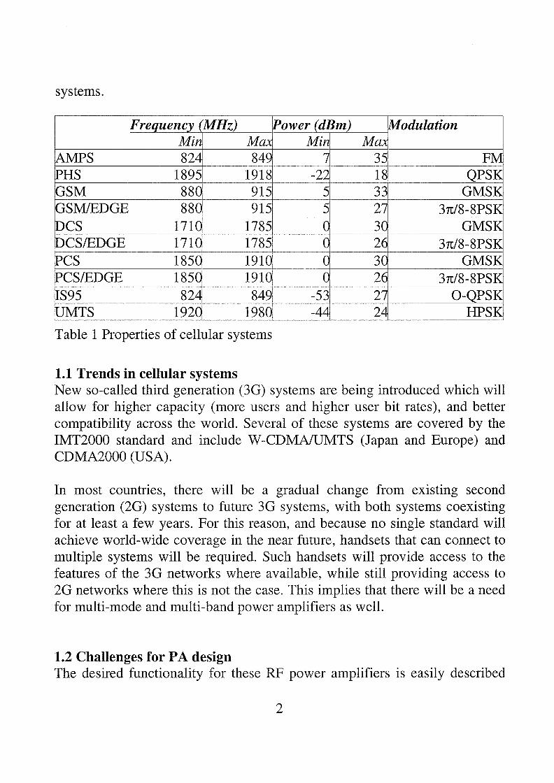
The handsets for these systems use a low-power transceiver to communicatewith a network of base stations using radio transmissions in the frequencyrange of 800MHz to 2500MHz, and transmit power levels in the range of10mW to 2W. Table 1 below shows an overview of important cellular
1
systems.
Frequency (‘MHz,) ~Power (‘dBm) WodulationMii~ Ma~ Min~ Ma~
AMPS 82~ 849 7~ 35 F~PHS 1895 1918 -22j 18 QPSKGSM 88C 915 5~ 33 GMSKGSM]EDGE 88C 915 5 27~ 37t/8-8P5KDCS 171C 1785 0 3~ GMSKDCS/EDGE 1710 1785 0 26~ 37t/8-8P5KPCS 1850 1910 0 30 GMSKPCSIEDGE 185~ 1910 0 26 3~t/8-8PSK1S95 824~ 849 -53 27 O-QPSKLJMTS 192Q 198Q -4~ 2~ HPSK
Table 1 Properties of cellular systems
Li Trends in cellular systemsNew so-called third generation (3G) systems are being introduced which willallow for higher capacity (more users and higher user bit rates), and bettercompatibility across the world. Several of these systems are covered by theIMT2000 standard and include W-CDMA/UMTS (Japan and Europe) andCDMA2000 (USA).
In most countries, there will be a gradual change from existing secondgeneration (2G) systems to future 3G systems, with both systems coexistingfor at least a few years. For this reason, and because no single standard willachieve world-wide coverage in the near future, handsets that can connect tomultiple systems will be required. Such handsets will provide access to thefeatures of the 3G networks where available, while still providing access to2G networks where this is not the case. This implies that there will be a needfor multi-mode and multi-band power amplifiers as well.
1.2 Challenges for PA designThe desired functionality for these RF power amplifiers is easily described
2
and modeled: it should accurately amplify an incoming RF signal by a fixed(or programmable) gain:
D — *13.‘out~ p i-in
With P0~ the output power, P1~ the input power, and G~ the power gain.
The simplicity of this desired functionality is apparent from many modemimplementations, which consist of relatively few active devices (starting at 2transistors).
Therefore, it might seem that the design of such a simple function requireslittle effort and deserves little attention. As with many other RF circuits incellular phones, the justification for all the effort that goes into their design isderived from the combination of:• the importance of these circuits to the overall performance of the handset• the many specifications that need to be achieved simultaneously
The power amplifier is important to the overall performance of the handsetsince it typically consumes the largest part of the power in a handset whenactive, and is therefore the most important factor in the talk time of a handset.For that reason, power efficiency is a very important specification of a PA.
This efficiency has to be achieved while still meeting the many specificationsrequired to have the handset work well within the system:• Linearity is becoming an important issue especially in newer systems that
use advanced modulation schemes to achieve better bandwidth efficiency• Robustness is important since the handset is part of a rather variable
environment, in which power supply voltage, load impedance,temperature, transmit frequency, and output power can vary quickly andsometimes over large ranges. Since the optimization of efficiency oftenresults in voltages and currents close to the reliability limits of thetechnology, significant changes in any of these parameters can result inperformance degradation or even complete failure of the device.Conversely, preventing such robustness problems often results in designswith voltages and currents that cannot be optimized for efficiency.
3
• Stability, especially under load mismatch conditions. Such conditions canfor example arise when the antenna environment changes.
• Noise, especially in the receive band of the system, since this affects thesensitivity of receivers in the system
• Spurious emissions, which can interfere with other electronic equipmentor with transmissions from other handsets or from basestations in the samesystem
• Thermal behavior, including performance impact of temperature changeson the handset, and impact on reliability
• Multi-mode multi-band functionality, which requires adjustable propertiesof the power amplifier, and/or switches and adjustable circuits around anumber of individual power amplifiers. This added complexity affects inturn the other specifications such as gain, linearity, output power, etc.
This paper will give an overview of these issues. In the next section, therelation between bandwidth efficiency, power amplifier linearity and powerefficiency will be discussed at system and circuit level.Section 3 describes the environment of the power amplifier, which is thebasis for relating the systems considerations of the previous section (2) to thePA issues in the next section (4).
Implementing the power amplifier is discussed in section 5, using a SiILTCCintegrated GSMIEDGE power amplifier module to demonstrate the relevantissues.
2. Bandwidth Efficiency, Power Efficiency and PA Linearity
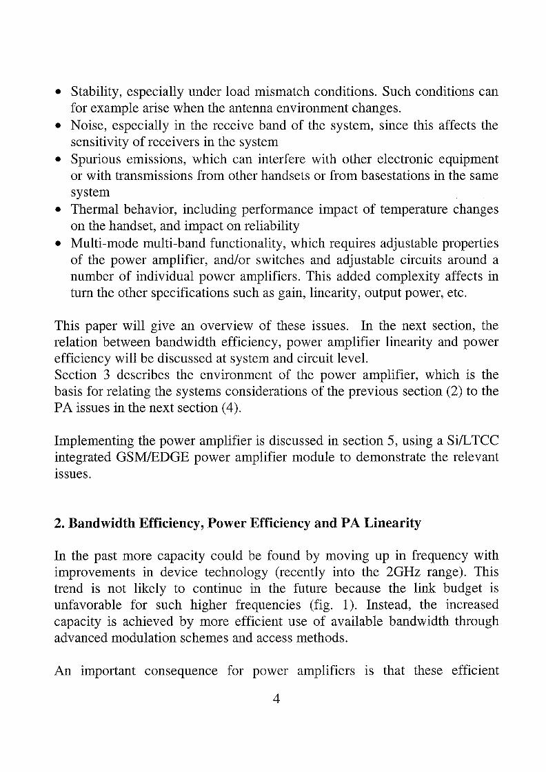
In the past more capacity could be found by moving up in frequency withimprovements in device technology (recently into the 2GHz range). Thistrend is not likely to continue in the future because the link budget isunfavorable for such higher frequencies (fig. 1). Instead, the increasedcapacity is achieved by more efficient use of available bandwidth throughadvanced modulation schemes and access methods.
An important consequence for power amplifiers is that these efficient
4
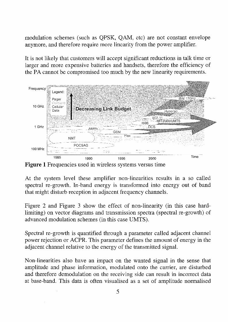
At the system level these amplifier non-linearities results in a so calledspectral re-growth. In-band energy is transformed into energy out of bandthat might disturb reception in adjacent frequency channels.
Figure 2 and Figure 3 show the effect of non-linearity (in this case hard-limiting) on vector diagrams and transmission spectra (spectral re-growth) ofadvanced modulation schemes (in this case UMTS).
Spectral re-growth is quantified through a parameter called adjacent channelpower rejection or ACPR. This parameter defines the amount of energy in theadjacent channel relative to the energy of the transmitted signal.
Non-linearities also have an impact on the wanted signal in the sense thatamplitude and phase information, modulated onto the carrier, are disturbedand therefore demodulation on the receiving side can result in incorrect dataat base-band. This data is often visualised as a set of amplitude normalised
modulation schemes (such as QPSK, QAM, etc) are not constant envelopeanymore, and therefore require more linearity from the power amplifier.
It is not likely that customers will accept significant reductions in talk time orlarger and more expensive batteries and handsets, therefore the efficiency ofthe PA cannot be compromised too much by the new linearity requirements.
FrequencyLegend
Pager
CellularData
10 GHz
1 GHz
100 MHz
Figure 1
--
lS95-. DCS
GSM -- -- -.
FlexN MT
POCSAG
1990 1995 20001985
Frequencies used in wireless systems versus time
Time
5
discrete I and Q values that represent the symbols being transmitted. Due todistortion the I and Q values of each symbol shift. The Error VectorMagnitude (EVM) is used to quantify this shift.
1_;~— — — — —
1.0— — — — —
0,8— — — — —
0.6—— — — —
0.4— —
~ 02-— - —
i~•0,4———~
-0,6—— — — —.
•0.8—— — — — —
-1.0—— —‘ — — —
-1.4-1.2-tO-O.8-06 -(,,4-O,2-0,0 0.2 0.4 0,6 0.8 1.0 1.3Inphase i(t(
Figure 2 Vector diagramtransmitter.
Figure 3 Vector diagram and spectrum of a hard-limited (near-constantenvelope) UMTS signal
ACPR and EVM are determined by the amplifier non-linearities incombination with the signal. For the various systems both the requirementson ACPR and EVM as well as the properties of the signal (Pout, peak-to-
1.3— fl F’
(1-tc)/Hz
and spectrum of an
15356250
ideal UMTS handset
‘0
~5625.0 Hz
B
-40.66—4500_FFT pthits 0182. AVG = 1,~
-50.00—
-55.00—
60.00— I -j
-65.00—
-70.00-~ -,
-75.00—
-80.00—
-05.00—
-00,00—
-95.00—
-100.00—10500_..1..1L I____________
Inph~oe 1(t)
I —
—
-15360000-10000000
-~III
‘ I
ioodoooo 15358250(~-Io(/Hz
6

average, power density distribution, ..) are different. This makes comparisonof linearity requirements for the various standards difficult.
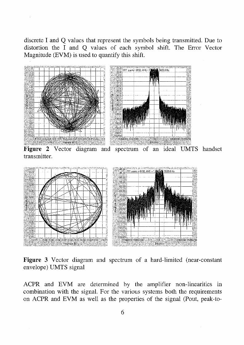
Figure 4 Due to distortion of the amplifier the symbols being transmitted,represented by their amplitude normalised I and Q values, are shifted. This isdefined as Error Vector Magnitude (EVM).
On the other hand, AM-to-AM and AM-to-PM conversion are inherentproperties of the circuit. For a given protocol ACPR and EVM are related tothe combination of AM-to-AM and AM-to-PM. Therefore a maximumallowable AM-to-AM requirement can not be defined independent of themaximum allowable AM-to-PM and visa versa. In practice a whole set ofAM-to-AM and AM-to-PM combination can be found that fulfil the ACPRand EVM requirements. A much larger set that doesn’t. Consequently, PAcircuit optimisation can best be done by optimising for the system parametersACPR and EVM rather than for AM-to-AM and AM-to-PM [2].
A single stage bipolar amplifier has several causes of non-linearity. We candistinguish contributions due to voltage saturation at the collector, transistorcurrent density variations, supply voltage variations at the transistor base andsupply voltage variations at the collector.
1.21 .0—o .8—0.0
0.2c~ 0.0
—0 . 2—0 . 4—0 .
—0.—1 .0—1 .2
Reference signal
(ideal IQ):~-~
~::-
R~~~~red signal
-~--~OL)QLD
cDNJ~o~
NJ ~J O~) .~ NJ0 N)
Phase error
7

2.1 Voltage saturation.Power amplifiers are optimised for optimum power added efficiency andlinearity. The collector load impedance at the fundamental frequency andharmonics is chosen such that at the maximum required output power thecomplete signal voltage headroom at the collector is used. Consequently, thetransistor is driven in saturation as much as possible up to the point wheresaturation becomes too severe. This trade-off is limited by the emitter ballastresistors needed for thermal stability and by the transistor collector resistanceand quasi saturation behaviour related to that.
2.2 Current density variationsAlthough power amplifiers for applications like cdmaOne, Edge, W-CDMAetc. are often referred to as linear amplifiers their behaviour is non-linear.Due to class A/B operation the culTent through an RF transistor, biasedtypically at 5OmA, can increase up to an average of 500mA at maximumoutput power. Under influence of the carrier envelope the transistoroperating point changes drastically. As a result the transistor input impedancevaries with the carrier envelope [3]. The impedance match with the source ispower dependent and thus varies with the envelope. This effect can be usedadvantageously. At power levels close to saturation the amplitude of the gaintends to drop down. When the source impedance match is optimal around thispower level and less optimum at lower power levels the gain can be flattenedout over a wider power level range [4].
2.3 Supply voltage variationsNon-linearity of the RF-transistor results in low frequency components in thecollector and base current. These low frequency components are related tothe data modulated on to the carrier. For Edge the modulation bandwidth is100kHz approximately. Any resistance in the power supply of the collectorwill result in low frequency supply voltage variations at the collector. At highpower levels this drives the RF-transistor further in to saturation. Therefore,proper LF-decoupling of the collector supply voltage is necessary forachieving maximum linearity.
8
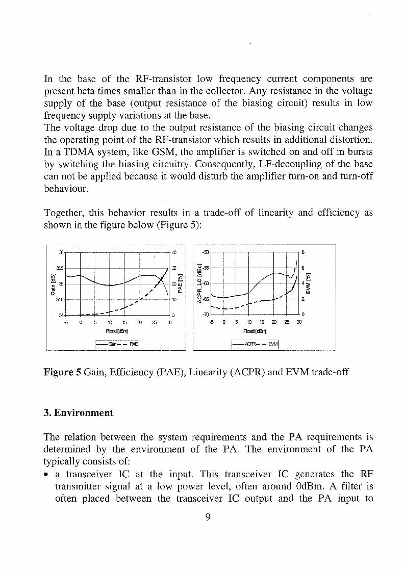
In the base of the RF-transistor low frequency current components arepresent beta times smaller than in the collector. Any resistance in the voltagesupply of the base (output resistance of the biasing circuit) results in lowfrequency supply variations at the base.The voltage drop due to the output resistance of the biasing circuit changesthe operating point of the RF-transistor which results in additional distortion.In a TDMA system, like GSM, the amplifier is switched on and off in burstsby switching the biasing circuitry. Consequently, LF-decoupling of the basecan not be applied because it would disturb the amplifier turn-on and turn-offbehaviour.
Together, this behavior results in a trade-off of linearity andshown in the figure below (Figure 5):
efficiency as
Figure 5 Gain, Efficiency (PAE), Linearity (ACPR) and EVM trade-off
3. Environment
The relation between the system requirements and the PA requirements isdetermined by the environment of the PA. The environment of the PAtypically consists of:• a transceiver IC at the input. This transceiver IC generates the RF
transmitter signal at a low power level, often around OdBm. A filter isoften placed between the transceiver IC output and the PA input to
CC,
C,
:E~::~E~.4c — ——
— ——
‘0
3J
10
0-5 0 5 10 15 a~ ~
Flc~d[c~1
— PPEj
~—-~---~I
~_1~ ~ ~ —~
>Iii
-5 05 10_—~
Flcai [cBij
9

eliminate noise from the transmitter IC outside the transmission band.• antenna interface circuits that can include matching circuits, isolator,
duplexer, switches, and diplexers to connect the PA to one or moreantennas
• a control IC that sets gain, biasing, and/or output power levels through anumber of control pins
• a power supply, which is often directly coming from the battery, but canalso be provided through a DC/DC converter
A typical PA environment is shown in the figure below (Fig. 6):
The duplexer is responsible for connecting the antenna to both the transmitterand receiver in such way that the energy from the transmitter is sent to theantenna only (and not the receiver), whereas the energy received by theantenna is sent to the receiver only (and not the transmitter). Depending onthe access and duplex methods of the system, the duplexer can beimplemented either as a traditional duplexer filter and/or through switches.The diplexer connects transceivers for different systems and/or bands to theantenna. Again, depending on the properties of the systems, this can be
Power/Gain!Mode Control
Figure 6 Environment of the PA
10
implemented through filters and/or switches.The isolator serves to protect the power amplifier from impedancemismatches at the duplexer input. This is not always necessary, e.g. for GSMtype systems this component is typically left out. By presenting the PA afixed and nominal load impedance independent of the actual input impedanceof the duplexer, the design of the PA can be further optimized since theinfluence of the load impedance on linearity, reliability and stability does nothave to be taken into account.
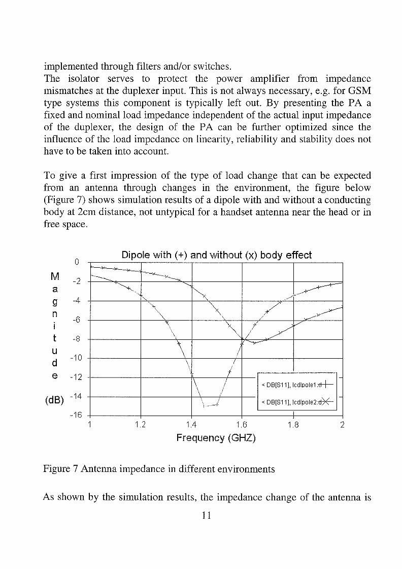
To give a first impression of the type of load change that can be expectedfrom an antenna through changes in the environment, the figure below(Figure 7) shows simulation results of a dipole with and without a conductingbody at 2cm distance, not untypical for a handset antenna near the head or infree space.
Magn
tU
de
(dB)-16
Figure 7 Antenna impedance in different environments
As shown by the simulation results, the impedance change of the antenna is
0Dipole with (+) and without (x) body effect
-4
-6
-8
-10
-12
-14
1 1 2 1.4 1.6
Frequency (GHZ)1.8
11
quite dramatic and results in large changes of the return loss, e.g. from —10dBto —2dB around 1.37GHz. This results in a reduction of transmitted powerfrom 90% to 37%. Considering all the effort spent on optimizing theefficiency of the PA, these numbers are very significant. Measurements onvarious antennas show that these numbers do occur in practice as well, and insome cases can be even worse.
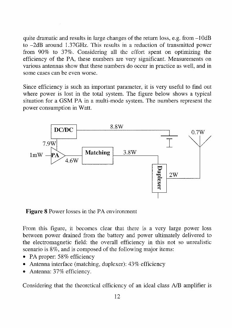
Since efficiency is such an important parameter, it is very useful to find outwhere power is lost in the total system. The figure below shows a typicalsituation for a GSM PA in a multi-mode system. The numbers represent thepower consumption in Watt.
1mW
From this figure, it becomes clear that there is a very large power lossbetween power drained from the battery and power ultimately delivered tothe electromagnetic field: the overall efficiency in this not so unrealisticscenario is 8%, and is composed of the following major items:• PA proper: 58% efficiency• Antenna interface (matching, duplexer): 43% efficiency• Antenna: 37% efficiency.
Considering that the theoretical efficiency of an ideal class A/B amplifier is
8.8W
Figure 8 Power losses in the PA environment
12
78%, it is obvious that the potential for improving overall efficiency byimproving the PA proper (e.g. by going to more expensive active devices) islimited. Instead, passive devices and the antenna are more obvious candidatesfor overall efficiency improvement.
4. Power amplifier
After taking into account the environment of the PA, what remains is anumber of issues and specifications that need to be achieved in the PA itself,through careful choices in the partitioning, implementation and technologies.
It is rather common to implement GSM power amplifiers as hybrids. Thisallows for usage of best combinations of active and passive technologies inorder to be able to meet severe specifications on reliability, ruggedness,stability, power added efficiency, size and cost. Moreover, a hybrid poweramplifier solutions is attractive because, due to the 5O~2 matching networks atinput and output and the on-module power supply decouplings, the amplifierfunction is well defined and therefore easily applicable.
Reliability (life-time) of a GSM amplifier is mainly related to the maximumtemperatures that occur. Especially for the recently defined class 12operation, with an on/off duty cycle of 50%, the solder between PCB andhybrid module, the glue to attach the die on the LTCC substrate and theAluminium interconnect of the die might approach critical temperaturevalues.
Moreover, the amplifier has to survive very severe conditions that mighthappen occasionally. For instance, the amplifier should not be damaged whenthe antenna is being disconnected while the battery is being charged andcollector voltages up to 20V may occur. This poses rather severerequirements on the collector-base breakdown voltage.
In a GSM handset the power amplifier dissipates a significant amount ofpower and thus determines the standby and talk time in to a great extend. Inparticular the final RF-transistor geometry and the output matching network
13

have to be designed for maximum power added efficiency [1]. The outputmatching network provides an optimum collector load impedance for thefundamental frequency as well as for the harmonics. It is realised by meansof High-Q microstrip lines, integrated on LTCC, and high-Q SMDcapacitors in order to minimise insertion losses.
For a dual mode GSMIEdge power amplifier additional requirements withrespect to linearity have to be met. There is not much design freedom foroptimising the linearity of a GSM/Edge amplifier when typical GSMspecifications have to be met anyway. In this example, the biasing of the RFtransistor in GSM mode has been made independent of the biasing in Edgemode. Optimum linearity is achieved by optimising the DC operating pointsof the three cascaded RF-transistors each.
5. Implementation
In this section we will discuss implementation details of the GSM]EDGE PA.This PA is relevant for a number of reasons:• This combination of systems in a single handset is likely to become
popular• It is an optimised combination of a saturated, strongly non-linear PA for
GSM mode and a linear PA for EDGE mode, with integrated modeswitching
• It is typical for many of the multi-mode multi-band power amplifiers thatwill be needed in the transition period between 2G and 3G systems.
The Edge protocol has been adopted as an evolutionary path for enhanceddata-rates and increased capacity in GSM. Edge is compatible to GSM in thesense that it operates in the same frequency bands and that it makes use of thesame channel bandwidth and channel spacing. The data-rate, however, hasbeen made a factor 3 higher by applying 37t/8 offset 8-PSK (non-constantenvelope) modulation and appropriate modulation filtering.The amplifier module consists of two fully independent RF line-ups (seeFigure 9). Each line-up consists of a 50 ohm input matching circuit, three
14
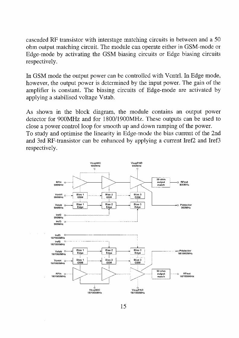
cascaded RF transistor with interstage matching circuits in between and a 50ohm output matching circuit. The module can operate either in GSM-mode orEdge-mode by activating the GSM biasing circuits or Edge biasing circuitsrespectively.
In GSM mode the output power can be controlled with Vcntrl. In Edge mode,however, the output power is determined by the input power. The gain of theamplifier is constant. The biasing circuits of Edge-mode are activated byapplying a stabilised voltage Vstab.
As shown in the block diagram, the module contains an output powerdetector for 900MHz and for 1800/1900MHz. These outputs can be used toclose a power control ioop for smooth up and down ramping of the power.To study and optimise the linearity in Edge-mode the bias current of the 2ndand 3rd RF-transistor can be enhanced by applying a current Iref2 and Iref3respectively.
VsupMIC VsupPAD900MHz 900MHz
RFout900MHz
Pdetector900MHz
15
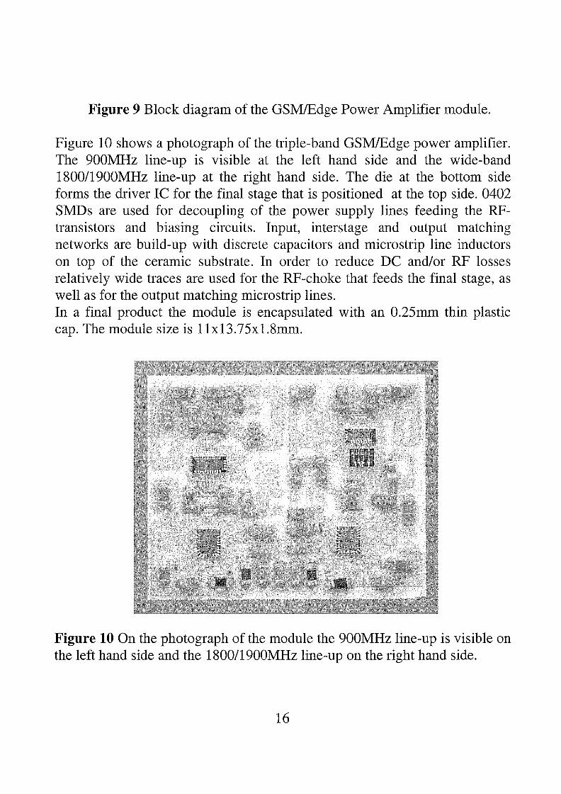
Figure 9 Block diagram of the GSM/Edge Power Amplifier module.
Figure 10 shows a photograph of the triple-band GSM!Edge power amplifier.The 900MHz line-up is visible at the left hand side and the wide-band1800/1900MHz line-up at the right hand side. The die at the bottom sideforms the driver IC for the final stage that is positioned at the top side. 0402SMDs are used for decoupling of the power supply lines feeding the RFtransistors and biasing circuits. Input, interstage and output matchingnetworks are build-up with discrete capacitors and microstrip line inductorson top of the ceramic substrate. In order to reduce DC and/or RF lossesrelatively wide traces are used for the RF-choke that feeds the final stage, aswell as for the output matching microstrip lines.In a final product the module is encapsulated with an 0.25mm thin plasticcap. The module size is 11x13.75x1.8mm.
~
Figure 10 On the photograph of the module the 900MHz line-up is visible onthe left hand side and the 1800/1900MHz line-up on the right hand side.
16
5.1 Output matching networkOn the left top side of the module the RC-choke to feed the 900MHz finalstage is visible. The choke is RF decoupled at the supply side and maderesonant using a capacitor located close to the collector bondwires. Theoutput matching network, located next right to the RF choke, consists ofseveral sections to transform the 50ohm load, in several steps, to an optimumcollector impedance of about 2 Ohm at the fundamental frequency andO.5+lOj at the second harmonic. Rejection of the second and third harmonicis obtained by series resonance of matching capacitors and their series selfinductance plus via inductance which gives notches in the transfer function.In simulations a typical insertion loss of 0.8dB can be obtained. Theattenuation at the second and third harmonic is typically 25dB and 35dBrespectively.
5.2 Thermal designUnder nominal operating conditions the amplifier module dissipates, duringthe power burst, approximately 3.5W when the amplifier output power is at amaximum of approx. 3.5W. Under antenna mismatch conditions combinedwith high battery supply voltage the power dissipation can be even twice thatvalue. Thermal stability is ensured by applying emitter ballast resistors.
The heat, mainly generated in the emitters of the final stage, is being spreadby the 200um thick silicon die and flows through the glue toward the dieattach area on top of the LTCC. Internal LTCC layers are used to partlyspread out the heat horizontally. The heat flows further through the copperfilled vias of the LTCC substrate towards the PCB that contains severallayers of copper to further spread out the heat into the telephone set. Themodule is designed for a thermal resistance of less than 30 KJW in order tokeep the maximum die temperature below 125°C, for a maximum mountingbase temperature of 85°C and a power dissipation of 7W in the pulse with anon/off duty cycle of 25%.
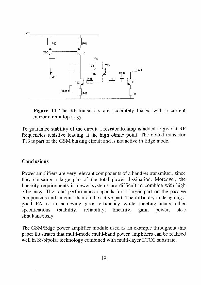
5.3 Biasing circuit topologyFigure 11 shows the circuit topology for biasing the 1st RF transistor in Edge
17
mode. The culTent ‘REFI drives, via the PNP min~or T60/T6i, the NPN currentmirror formed by T62 and Ti. Emitter degeneration resistances R60/R6 1 areadded to increase output resistance of the PNP current mirror T601T6 1 inorder to reduce the supply voltage dependancy and to improve matching ofthis current mirror [5]. T63 improves the accuracy of the NPN current mirrorfactor with its current multiplication factor of beta.
The resistors R63 and R62 are added to make the topology of the left handside of the NPN mirror equal to the topology of right hand side where Ri6can be used to provides RF isolation between Ti and the biasing circuit andRi is used to degenerate Ti. Summing voltages around the loop includingT62 and Ti we find
J~62R6, + ~ 1n(~~) + 1862R63 = I~R + ~ 1n(~) + I,1R( ( 1)562 SI
Making the assumption that p6, = = = p >> i we find that
‘Cl =~ (2)
Since i~, = , defined by emitter area ratios, the solution to (2) is
R+~
‘Cl = - R ‘REFI =‘81RJ~Fl
1/3
which is achieved by R6, = 18R, = 18x7 = 126≤2 and R63 = 18R16 = 18x100 = 1800Q
As a result the last term in (2) goes to zero which makes the biasing of Tialmost temperature independent.
i8
Vcc
RFout
Figure 11 The RF-transistors are accurately biased with a currentmirror circuit topology.
To guarantee stability of the circuit a resistor Rdamp is added to give at RFfrequencies resistive loading at the high ohmic point. The dotted transistorT13 is part of the GSM biasing circuit and is not active in Edge mode.
Conclusions
Power amplifiers are very relevant components of a handset transmitter, sincethey consume a large part of the total power dissipation. Moreover, thelinearity requirements in newer systems are difficult to combine with highefficiency. The total performance depends for a larger part on the passivecomponents and antenna than on the active part. The difficulty in designing agood PA is in achieving good efficiency while meeting many otherspecifications (stability, reliability, linearity, gain, power, etc.)simultaneously.
The GSMIEdge power amplifier module used as an example throughout thispaper illustrates that multi-mode multi-band power amplifiers can be realisedwell in Si-bipolar technology combined with multi-layer LTCC substrate.
T60
R61
Vcc
I T13
REin
Ri
19

AcknowledgementsThis paper is based on insights built up in several teams throughout Philips,including the Philips Semiconductor PA development teams in Sagamihara(Japan), Mansfield (U.S.A.) and Nijmegen (The Netherlands), as well as thePhilips Research Integrated Transceiver group in Eindhoven (TheNetherlands).The GSM/Edge power amplifier module could only be realised with the helpfrom enthusiastic team members. Being aware that their contributions to thesuccess of this project were very essential I would like to thanks DimaPrikhodko for his work on IC circuit development, Skule Pramm and GerdKahmen for designing the substrate and optimising the module andChristophe Chanlo for simulating ACPR and EVM. Last but not least I wouldlike to thanks Reza Mahmoudi for the enlightened discussions we had and fordeveloping dedicated ACPR and EVM simulation tools.
References:[1] F. van Rijs, R. Dekker, H.A. Visser, H.G.A. Huizing, D. Hartskeerl,P.H.C. Magnee, R.Dondero. “Influence of output impedance on power addedefficiency of Si-bipolar power transistor” International microwavesymposium digest, Volume 3, June 11-16, 2000
[2] Private communication with Reza Mahmoudi
[3] Keng Leong Fong and Robert G. Meyer, “High-Frequency NonlinearityAnalysis of Common-Emitter and Differential-Pair TransconductanceStages”, IEEE journal of solid-stade circuits vol 33, no 4, April 1998
[4] R. Mahmoudi, “Multi-Disciplinary design method for 2.5 generation ofmobile communication systems” to be published in September 2001, TwenteUniversity Press.
[5] Paul R.Gray and Robert G. Meyer, “Analysis and Design of AnalogIntegrated Circuits”, second editions, John Wiley & Sons 1984
20