design economics. ic designer should able to predict the cost and the time to design a particular...
TRANSCRIPT

Design Economics
Design Economics
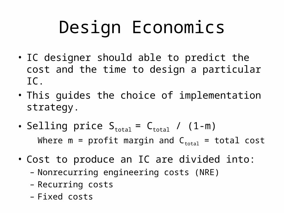
• IC designer should able to predict the cost and the time to design a particular IC.
• This guides the choice of implementation strategy.
• Selling price Stotal = Ctotal / (1-m)
Where m = profit margin and Ctotal = total cost
• Cost to produce an IC are divided into:– Nonrecurring engineering costs (NRE)– Recurring costs– Fixed costs

Non-recurring Engineering Costs
• Cost once spent during the design of an IC, they include:– Engineering design cost– Prototype manufacturing cost– i.e., Ftotal = Etotal + Ptotal
• NRE can be viewed as an investment for which there is a required rate of return.
• Engineering design costs, include:– Personnel costs– Support costs
• Prototype manufacturing costs, include:– Mask cost– Test fixture costs– Package tooling

• The personnel cost include labor for:– Architectural design– Logic capture– Simulation for functionality– Layout of modules and chip– Timing verification– DRC and tapeout procedures– Test generation
• The support costs are:– Computer costs– CAD software costs– Training

Recurring Costs
• The cost that recurs every time an IC is sold.• The total cost is Ct = Cprocess + Cpack + Ctest
– Cprocess = W / (N.Yd.Ypack.)
• Fabrication– Wafer cost / (Dice per wafer * Yield)– Wafer cost: $500 - $3000– Dice per wafer: – Yield: Y = e-AD
• For small A, Y 1, cost proportional to area• For large A, Y 0, cost increases exponentially
• Packaging• Test

Fixed Costs
• Data sheets and application notes• Marketing and advertising

Schedule• Estimate the design cost and design time for the
system.• Selecting the strategy by which the ICs will be
available in the right time and price.• Experienced person. • To estimate schedule some idea of the amount
effort required to complete the design.• Schedule is a function of personpower.• Methods for improving the schedules:
– Using a high productivity design method– Improving the productivity of a given technique– Decreasing the complexity of the design task by
partitioning

Personpower • Tasks required are:• Architectural design• HDL capture• Functional verification• PAR• Timing verification, signal integrity, reliability
verification• DRC and tapeout procedures• Test generation
Example
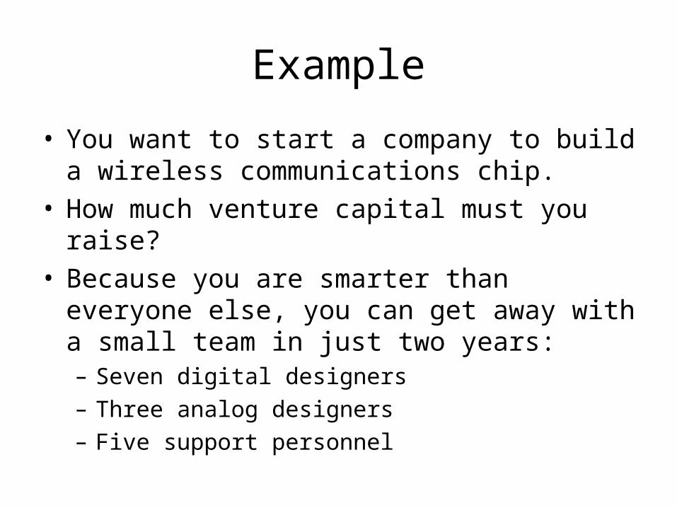
• You want to start a company to build a wireless communications chip.
• How much venture capital must you raise?• Because you are smarter than everyone else,
you can get away with a small team in just two years:– Seven digital designers– Three analog designers– Five support personnel

Solution• Digital designers:
– salary
– overhead
– computer
– CAD tools
– Total:
• Analog designers– salary
– overhead
– computer
– CAD tools
– Total:
• Support staff– salary– overhead– computer– Total:
• Fabrication– Back-end tools: – Masks: – Total:
• Summary
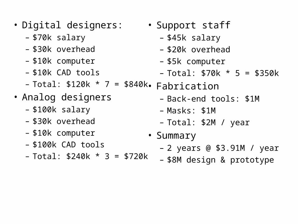
• Digital designers:– $70k salary
– $30k overhead
– $10k computer
– $10k CAD tools
– Total: $120k * 7 = $840k
• Analog designers– $100k salary
– $30k overhead
– $10k computer
– $100k CAD tools
– Total: $240k * 3 = $720k
• Support staff– $45k salary– $20k overhead– $5k computer– Total: $70k * 5 = $350k
• Fabrication– Back-end tools: $1M– Masks: $1M– Total: $2M / year
• Summary– 2 years @ $3.91M / year– $8M design & prototype
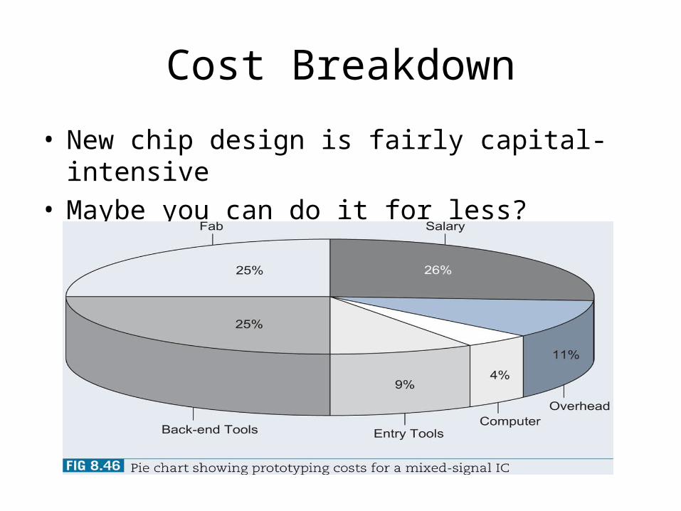
Cost Breakdown
• New chip design is fairly capital-intensive• Maybe you can do it for less?


Special-purpose Subsystems

Agenda• Packaging
– Package options– Chip-to-package connections– Package parasitics– Heat dissipation
• Power Distribution– On-chip power distribution network– Supply noise
• I/O– Basic I/O pad circuits
• Clock– Clock system architecture– Global clock generation & distribution– Local clock gaters
Packaging
• Package functions:– Electrical connection of signals and power from chip to
board, with little delay or distortion– Mechanical connection of chip to board– Removes heat produced on chip– Protects chip from mechanical damage– Compatible with thermal expansion– Inexpensive to manufacture and test

Package Options
• Through-hole vs. surface mount

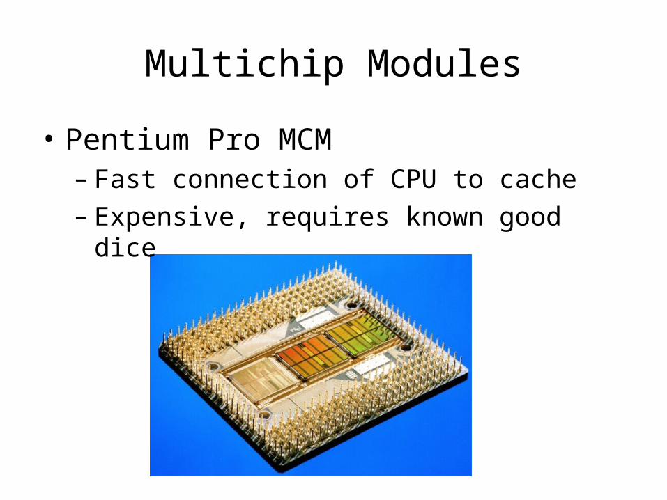
Multichip Modules
• Pentium Pro MCM– Fast connection of CPU to cache– Expensive, requires known good dice

Chip-to-Package Bonding
• Traditionally, chip is surrounded by pad frame:– Metal pads on 100 – 200 m pitch– Gold bond wires attach pads to package– Lead frame distributes signals in package– Metal heat spreader helps with cooling

Advanced Packages
• Metal leads contribute parasitic inductance and coupling capacitors to their neighbors
• Fancy packages have many signal, power layers– Like tiny printed circuit boards
• Flip-chip places connections across surface of die rather than around periphery– Top level metal pads covered with solder balls– Chip flips upside down– Carefully aligned to package (done blind!)– Heated to melt balls– Introduces new testing problems

Package Parasitics
Chip
Signal P
ins
PackageCapacitor
Signal P
ads
ChipVDD
ChipGND
BoardVDD
BoardGND
Bond Wire Lead Frame
Package
• Use many VDD, GND in parallel
– Inductance, IDD

• Bond wires and lead frame contribute parasitic inductance to the signal traces.
• They also have mutual inductance and capacitive coupling to nearby signal traces, causing crosstalk when multiple signal switch.
• VDD & GND wires also have inductance from both bond wires and lead frame.
• They have nonzero resistance, which becomes important for chips drawing large supply current
• High performances packages often include bypass capacitors between VDD & GND.

Heat Dissipation
• 60 W light bulb has surface area of 120 cm2
• Itanium 2 die dissipates 130 W over 4 cm2
– Chips have enormous power densities– Cooling is a serious challenge
• Advances in heat sinks, fans, packages have raised the practical limit for heat removal from about 8 W in 1985 to nearly 100 W today for affordable packaging.
• Package spreads heat to larger surface area– Heat sinks may increase surface area further– Fans increase airflow rate over surface area– Liquid cooling used in extreme cases ($$$)

• Temperature difference between transistor junctions and the ambient air is, T = jaP– T: temperature rise on chip
– ja: thermal resistance of chip junction to ambient
– P: power dissipation on chip
• Thermal resistances combine like resistors– Series and parallel
• ja = jp + pa
– Series combination
Thermal Resistance

Example
• Your chip has a heat sink with a thermal resistance to the package of 4.0° C/W.
• The resistance from chip to package is 1° C/W.• The system box ambient temperature may reach
55° C.• The chip temperature must not exceed 100° C.• What is the maximum chip power dissipation?
• Solution is (100-55 C) / (4 + 1 C/W) = 9 W

Power Distribution
• Power Distribution Network functions:– Carry current from pads to transistors on chip– Maintain stable voltage with low noise– Provide average and peak power demands– Provide current return paths for signals– Avoid electromigration & self-heating wearout– Consume little chip area and wire– Easy to lay out

Power Requirements• VDD = VDDnominal – Vdroop
• Want Vdroop < +/- 10% of VDD
• L di/dt of bond wire and IR drop across on-chip wires are often a major source of supply noise
• Sources of Vdroop– IR drops– L di/dt noise
• IDD changes on many time scales
clock gating
Time
Average
Max
Min
Power

IR Drops:• Resistance of power supply network includes:
– resistance of the on-chip wires and vias, – resistance of bond wires or solder bumps to the package, – resistance of the package planes,– resistance of the PCB planes
• IR drops arise from both average and instantaneous current requirements.
Ldi/dt Noise: • Inductance of power supply dominated by the inductance
of the bond wires• Modern packages devote many of their pins to power
and ground to minimize supply inductance• Two sources of current transients are switching I/O
signals and changes between idle and active mode in the chip core

On-chip Bypass Capacitance
• The bypass capacitance is distributed across the chip so that a local spike in current can be supplied from nearby bypass capacitance rather than through the resistance of the overall power grid.
• power distribution network doesn’t really need to carry all of the peak current.
• Much of the difference between peak and average current may be supplied by local, on-chip bypass capacitors.
• On-chip bypass capacitors can reduce the amount of metal needed for distribution.
• It also greatly reduces the di/dt drawn from the package.

Symbiotic Bypass Capacitors
• Where are the bypass capacitors in this picture?• Gates that are not switching at a given instant in time act
as symbiotic bypass capacitors• If only one gate in 60 switches at a given instant, the
bypass capacitance is 30 times the switched capacitance

Power System Model
• Power comes from regulator on system board:– Board and package add parasitic R and L– Bypass capacitors help stabilize supply voltage– But capacitors also have parasitic R and L
• Simulate system for time & frequency responses
VoltageRegulator
Printed CircuitBoard Planes
Packageand Pins
SolderBumps
BulkCapacitor
CeramicCapacitor
PackageCapacitor
On-ChipCapacitor
On-ChipCurrent Demand
VDD
Chip
PackageBoard

Input / Output
• Input/Output System functions:– Communicate between chip and external world– Drive large capacitance off chip– Operate at compatible voltage levels– Provide adequate bandwidth– Limit slew rates to control di/dt noise– Protect chip against electrostatic discharge– Use small number of pins (low cost)
I/O Pad Design
• Pad Types:– VDD and GND
– Output– Input– Bidirectional– Analog

VDD and GND Pads
• High-performance chips devote about half of their pins to power and ground.
• This large number of pins is required to carry the high current and to provide low supply inductance.
• Largest sources of noise in many chips is the ground bounce caused when the output pads switch.
• The pads must rapidly charge the large external capacitive loads, causing a big current spike and high Ldi/dt noise.
• The dirty power and ground lines serving the output pads are separated from the main power grid to reduce the coupling of I/O-related noise into the core.

Output Pads
• Drive large off-chip loads (2 – 50 pF)– With suitable rise/fall times– Requires chain of successively larger buffers
• Output transistors have gates longer than normal to prevent avalanche breakdown damage and over voltage is applied to the drains.
• Guard rings to protect against latchup– Noise below GND injects charge
into substrate– Large nMOS output transistor– p+ inner guard ring– n+ outer guard ring
• In n-well

Input Pads
• Level conversion– Higher or lower off-chip V– May need thick oxide gates
• Noise filtering– Schmitt trigger
– Hysteresis changes VIH, VIL
• Protection against electrostatic discharge
AY
VDDH
VDDLA Y
VDDL
A Y
weak
weak
A
Y

ESD Protection
• Static electricity builds up on your body– Shock delivered to a chip can fry thin gates– Must dissipate this energy in protection circuits before
it reaches the gates
• ESD protection circuits– Current limiting resistor– Diode clamps
• ESD testing– Human body model– Views human as charged capacitor
PADR
Diodeclamps
Thingate
oxides
Currentlimitingresistor
DeviceUnderTest
1500
100 pF

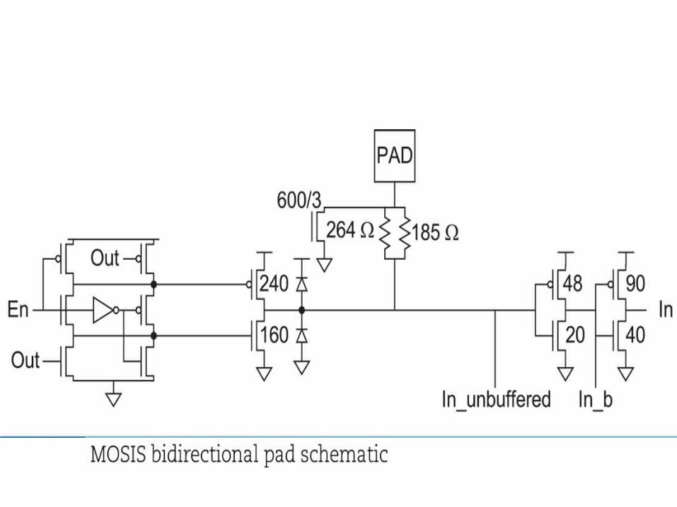
Bidirectional Pads
• Need tristate driver on output:– Use enable signal to set direction– Optimized tristate avoids huge series transistors
PAD
Din
Dout
En
Dout
En Y
Dout
NAND
NOR
Improved tri-state
buffer
Analog Pads
• Pass analog voltages directly in or out of chip:– No buffering– Protection circuits must not distort voltages
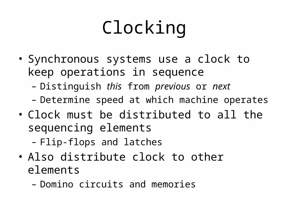
Clocking
• Synchronous systems use a clock to keep operations in sequence– Distinguish this from previous or next– Determine speed at which machine operates
• Clock must be distributed to all the sequencing elements– Flip-flops and latches
• Also distribute clock to other elements – Domino circuits and memories


Clock Distribution
• On a small chip, the clock distribution network is just a wire– And possibly an inverter for clkb
• On practical chips, the RC delay of the wire resistance and gate load is very long– Variations in this delay cause clock to get to different
elements at different times– This is called clock skew
• Most chips use repeaters to buffer the clock and equalize the delay– Reduces but doesn’t eliminate skew

Review: Skew Impact
setup skew
sequencing overhead
hold skew
pd c pcq
cd ccq
t T t t t
t t t t
• Ideally full cycle is available for work• Skew adds sequencing overhead• Increases hold time too

Solutions
• Reduce clock skew– Careful clock distribution network design– Plenty of metal wiring resources
• Analyze clock skew– Only budget actual, not worst case skews– Local vs. global skew budgets
• Tolerate clock skew– Choose circuit structures insensitive to skew

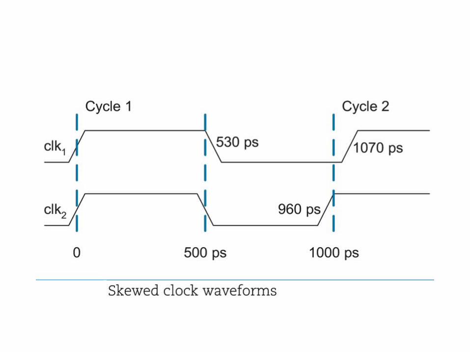
Clock Skew Sources
• Clock Skew Sources are: – systematic, – random, – drift, and – jitter
• Note some engineers do not report jitter as part of the skew.

Example
• Skew comes from differences in gate and wire delay– With right buffer sizing, clk1 and clk2 could ideally
arrive at the same time.– But power supply noise changes buffer delays
– clk2 and clk3 will always see RC skew
3 mm
1.3 pF
3.1 mmgclk
clk1
0.5 mm
clk2clk3
0.4 pF 0.4 pF

Clock System Architecture
Synchronous chip interface with PLL

Phase-locked loop block diagram


Global Clock Distribution Networks
• Grids
• H-trees
• Spines
• Ad-hoc
• Hybrid

Clock Grids
• A clock grid is a mesh of horizontal and vertical wires driven from the middle or edges.
• Use grid on two or more levels to carry clock.• Make wires wide to reduce RC delay.• Ensures low skew between nearby points.• But possibly large skew across die.• Grids compensate for random skew.• Grids consume a large amount of metal resources and
hence a high switching capacitance and power consumption.

Alpha Clock Grids
PLL
gclk grid
Alpha 21064 Alpha 21164 Alpha 21264
gclk grid
Alpha 21064 Alpha 21164 Alpha 21264
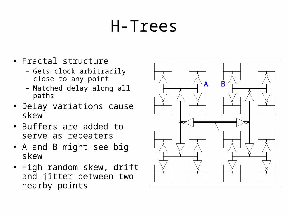
H-Trees
• Fractal structure– Gets clock arbitrarily close to
any point– Matched delay along all paths
• Delay variations cause skew• Buffers are added to serve
as repeaters• A and B might see big skew• High random skew, drift and
jitter between two nearby points
A B
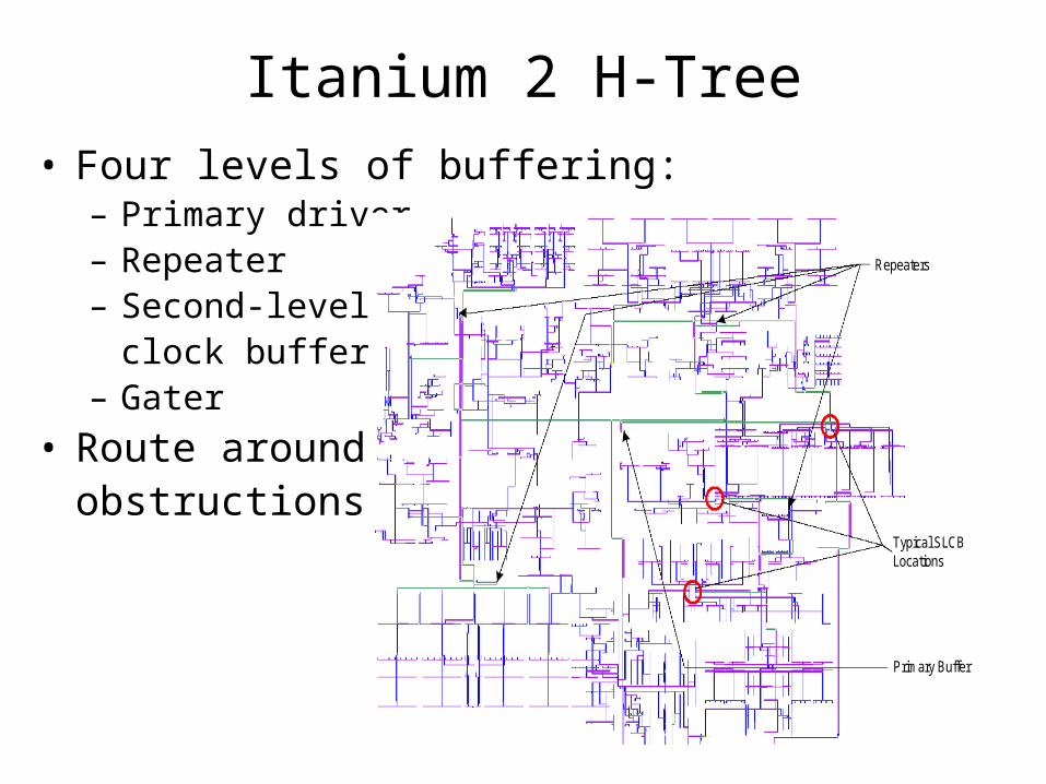
Itanium 2 H-Tree• Four levels of buffering:
– Primary driver– Repeater– Second-level
clock buffer– Gater
• Route aroundobstructions
Primary Buffer
Repeaters
Typical SLCBLocations

Ad-hoc
• The clock is routed haphazardly with some attempt to equalize wire lengths or add buffers to equalize delay.
• Have low systematic skews because the buffer sizes can be adjusted until nominal delays are nearly equal.
• Subject to random skew.
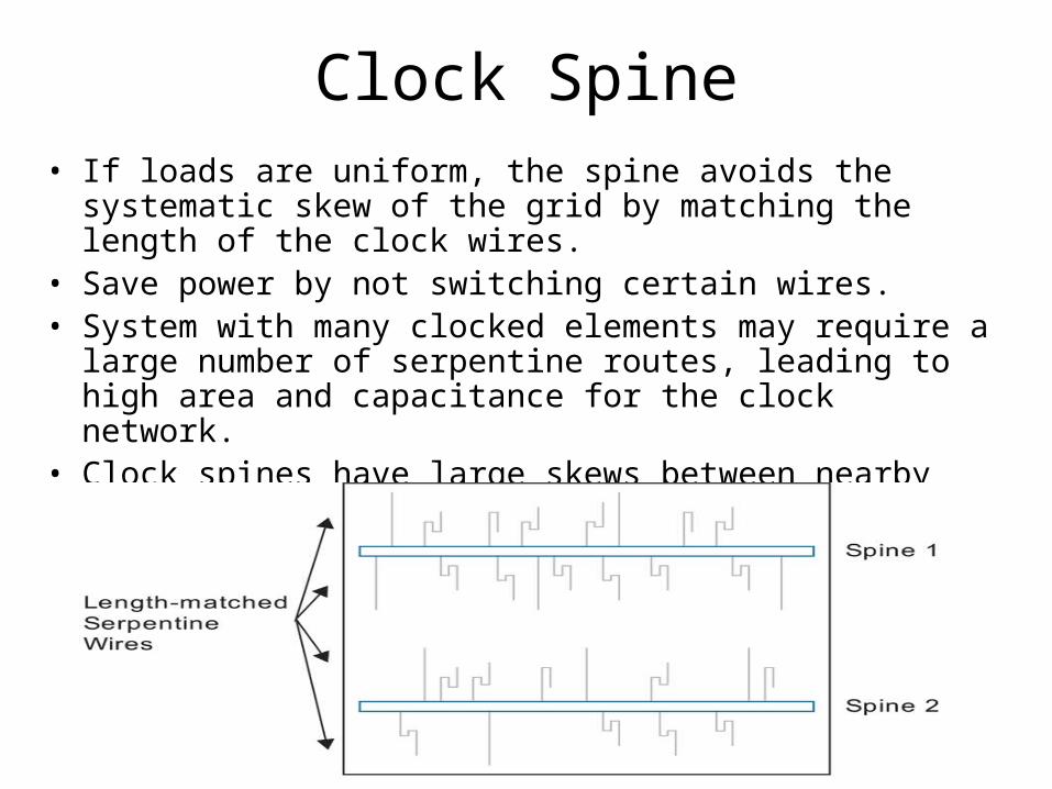
• If loads are uniform, the spine avoids the systematic skew of the grid by matching the length of the clock wires.
• Save power by not switching certain wires.• System with many clocked elements may require a large
number of serpentine routes, leading to high area and capacitance for the clock network.
• Clock spines have large skews between nearby elements driven by different serpentines.
Clock Spine

Hybrid Networks
• Use H-tree to distribute clock to many points.• Tie these points together with a grid.• Hybrid combination of H-tree and grid offers lower skew.• Hybrid approach has lower systematic skew, less
susceptible to skew from non-uniform load distribution.• Hybrid approach is regular, making layout of well-
controlled transmission line structures easier.
• Ex: IBM Power4, PowerPC– H-tree drives 16-64 sector buffers– Buffers drive total of 1024 points– All points shorted together with grid

Clock Generation
clken
1
2
3
4

• Local Clock Gaters receives the global clock and produce the physical clocks required by clocked elements.
• Clock gaters are often used to stop or gate the clock to unused blocks of logic to save power.
• Different clock gaters are:– Enabled or Gated clock– Stretched clocks– Nonoverlapping clocks– Complementary clock– Delayed, Pulsed clocks– Clock Doubler– Clock Buffer
Local Clock Gaters
