design example report - power
TRANSCRIPT

Power Integrations
5245 Hellyer Avenue, San Jose, CA 95138 USA. Tel: +1 408 414 9200 Fax: +1 408 414 9201
www.powerint.com
Design Example Report
Title 20 W Single Output, Power Factor Corrected LED Driver Using TOP247YN
Specification 85 VAC – 277 VAC Input; 12 V (12 V - 14 V LED Array), 1.67 A Output
Application LED Driver
Author Applications Engineering Department
Document Number
DER-168
Date October 28, 2009
Revision 1.2
Summary and Features Single stage PFC based constant voltage, constant current output power
supply Universal input range allows single design to be used worldwide Meets ENERGY STAR minimum PF requirement of 0.9 for commercial
environment (0.9 worst case at 277 VAC) Meets harmonic content limits as specified in IEC 61000-3-2 for Class C Meets EN55015 B conducted EMI limits with >8 dBµV margin Fully fault protected
Auto-restart withstands shorted output indefinitely Integrated thermal shutdown protects the entire supply Operates with no-load indefinitely
Full load: 6 rows of 4 diodes part# LW W5SG/GYHY-5K8L-Z PATENT INFORMATION The products and applications illustrated herein (including transformer construction and circuits external to the products) may be covered by one or more U.S. and foreign patents, or potentially by pending U.S. and foreign patent applications assigned to Power Integrations. A complete list of Power Integrations' patents may be found at www.powerint.com. Power Integrations grants its customers a license under certain patent rights as set forth at <http://www.powerint.com/ip.htm.

DER-168 20 W Single Output, LED Driver – TOP247YN 28-Oct-09
Page 2 of 28
Power Integrations Tel: +1 408 414 9200 Fax: +1 408 414 9201 www.powerint.com
Table of Contents 1 Introduction.................................................................................................................3 2 Power Supply Specification ........................................................................................4 3 Schematic...................................................................................................................5 4 PCB Layout ................................................................................................................6 5 Circuit Description ......................................................................................................7
5.1 Input EMI Filtering ...............................................................................................7 5.2 TOPSwitch Primary .............................................................................................7 5.3 Output Rectification .............................................................................................8 5.4 Output Feedback.................................................................................................8
5.4.1 Constant Voltage Operation .........................................................................8 5.4.2 Constant Current Operation .........................................................................9
5.5 Soft-Start .............................................................................................................9 6 Bill of Materials .........................................................................................................10 7 Transformer Specification.........................................................................................12
7.1 Electrical Diagram .............................................................................................12 7.2 Electrical Specifications.....................................................................................12 7.3 Materials............................................................................................................12 7.4 Transformer Build Diagram ...............................................................................13 7.5 Transformer Construction..................................................................................13
8 Transformer Design Spreadsheet.............................................................................14 9 Performance Data ....................................................................................................17
9.1 Efficiency ...........................................................................................................17 9.2 Line Regulation .................................................................................................17 9.3 Harmonic Content .............................................................................................18 9.4 Harmonic Content in Percentage of Fundamental.............................................18 9.5 Power Factor Vs Line Voltage at Full Load .......................................................19
10 Thermal Performance ...........................................................................................20 11 Waveforms............................................................................................................21
11.1 Drain Voltage and Current, Normal Operation...................................................21 11.2 Output Voltage Start-up Profile..........................................................................22 11.3 Drain Voltage and Current Start-up Profile ........................................................22 11.4 Output Ripple Measurements............................................................................23
11.4.1 Ripple Measurement Technique ................................................................23 11.4.2 Measurement Results ................................................................................24
12 Surge Test ............................................................................................................25 12.1 Surge Test Results with 1.2/50us Waveform.....................................................25 12.2 Surge Test Results with 0.5us-100 kHz Ring-Waveform...................................25
13 Conducted EMI .....................................................................................................26 14 Revision History ....................................................................................................27 Important Note: Although this board is designed to satisfy safety isolation requirements, the engineering prototype has not been agency approved. Therefore, all testing should be performed using an isolation transformer to provide the AC input to the prototype board.

28-Oct-09 DER-168 20 W Single Output, LED Driver – TOP247YN
Page 3 of 28
Power Integrations Tel: +1 408 414 9200 Fax: +1 408 414 9201
www.powerint.com
1 Introduction The document presents a power supply design to be used in LED Lighting applications. The design input voltage range is 85 to 277 VAC.
Figure 1 – Populated Circuit Board Photograph.

DER-168 20 W Single Output, LED Driver – TOP247YN 28-Oct-09
Page 4 of 28
Power Integrations Tel: +1 408 414 9200 Fax: +1 408 414 9201 www.powerint.com
2 Power Supply Specification The table below represents the minimum acceptable performance of the design. Actual performance is listed in the results section.
Description Symbol Min Typ Max Units Comment
Input Voltage VIN 85 277 VAC 2 Wire – no P.E.
Frequency fLINE 47 50/60 64 Hz
Output
Output Voltage 1 VOUT1 12 18 V
Output Ripple Voltage 1 VRIPPLE1 mV 20 MHz Bandwidth
Output Current 1 IOUT1 1.67 A
Total Output Power
Continuous Output Power POUT 20 W
Environmental
Conducted EMI Meets EN55015B
Safety Designed to meet IEC950, UL1950 Class II
Surge 1 kV 1.2/50 s Surge, IEC 61000-4-5,
Series Impedance: Common Mode: 12
Surge 0.5 kV 1.2/50 s Surge, IEC 61000-4-5,
Series Impedance: Differential Mode: 2
Ring-wave 2.5 kV 0.5 s-100KHz Ring-wave IEEE
C.62.41-1991, Class A, Differential and Common Mode
Ambient Temperature TAMB 0 50 oC Free Convection, Sea Level
28-Oct-09 DER-168 20 W Single Output, LED Driver – TOP247YN
Page 5 of 28
Power Integrations Tel: +1 408 414 9200 Fax: +1 408 414 9201
www.powerint.com
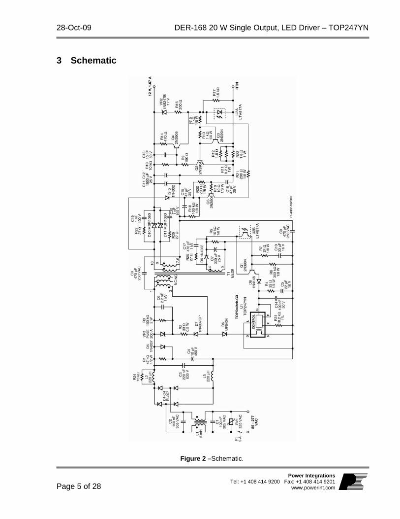
3 Schematic
Figure 2 –Schematic.

DER-168 20 W Single Output, LED Driver – TOP247YN 28-Oct-09
Page 6 of 28
Power Integrations Tel: +1 408 414 9200 Fax: +1 408 414 9201 www.powerint.com
4 PCB Layout
Figure 3 – PCB Layout.
28-Oct-09 DER-168 20 W Single Output, LED Driver – TOP247YN
Page 7 of 28
Power Integrations Tel: +1 408 414 9200 Fax: +1 408 414 9201
www.powerint.com
5 Circuit Description This design uses a discontinuous mode flyback power supply fed from an input stage with minimal capacitance. With a fixed duty cycle over an AC line cycle, this allows the peak drain current envelope, and therefore the input current, to follow the input AC voltage waveform to give high power factor and low harmonic content. Although this simple configuration gives both output regulation and power factor correction in a single stage converter, it does require higher peak drain currents compared to a standard power supply with substantiation input capacitance. Detailed descriptions of each function block are given below.
5.1 Input EMI Filtering In addition to the standard filtering (C1 and L1), L2 and L3 were added to provide increased differential mode filtering and surge withstand capability. This was required due to the small value of input capacitance (C3) and associated increase in switching currents seen by the AC input. Common mode filtering is provided by L1, C8 and C9. Together with transformer E-Shields (that reduce the source of EMI common mode currents), this allows the design to pass EN55015 B with good margin.
5.2 TOPSwitch Primary On application of the AC input, the combination of the in-rush current to charge C1, C2 and C3, together with the inductance in the AC line, causes a voltage spike that appears across C3. In a design with a large input capacitance, this voltage is negligible; however, here the voltage spike is sufficiently large to exceed the BVDSS rating of the MOSFET within TOP247YN. To prevent this, capacitor C4 and D5 limit the maximum voltage while R1 is the bleeder to discharge this capacitor on AC removal. The discontinuous mode of operation needed for high power factor increases the primary RMS current for a given output power. Selecting a larger TOPSwitch device (TOP247YN) than needed for power delivery offsets increases RMS current by reducing the RDSON conduction losses and giving higher efficiency and reduced dissipation. This was critical in this design in order to meet the maximum operating ambient of 50 °C. As the DC input voltage across C3 falls to zero during normal operation, D6 was added in series with the drain to prevent the DRAIN ringing below SOURCE and reverse biasing the device. As reverse biasing of the device is not permitted, this diode must be used. To provide high power factor using a single stage flyback converter, it is necessary to maintain the duty cycle of the MOSFET constant over a single AC line cycle (low bandwidth).

DER-168 20 W Single Output, LED Driver – TOP247YN 28-Oct-09
Page 8 of 28
Power Integrations Tel: +1 408 414 9200 Fax: +1 408 414 9201 www.powerint.com
As the control characteristic of TOPSwitch-GX is CONTROL (C) pin current to duty cycle (of the internal MOSFET), this requires that the current into the C pin must be held constant. The simplest way to achieve this would be to use a very large value of CONTROL pin capacitance (C5). However, a large value of C5 causes a large startup time and also a large startup overshoot. To overcome this difficulty, an emitter follower (Q1) was used as an impedance transformer with a capacitor C10 in its base. Looking into the emitter of Q1, C10 appears to be larger (C10 x Q1hfe), and R6 appears to be smaller (R6 / Q1hfe). Capacitor C10, together with R6, sets the dominant pole of the circuit at approximately 0.01 Hz. Resistor R7 provides loop compensation, creating a zero at approximately 44 Hz, which gives additional phase starting at 4 Hz to improve phase margin at gain crossover. Gain crossover occurred in this design at approximately 30 Hz. Higher bandwidth is undesirable as this degrades power factor by increasing the third harmonic content in the input current waveform. Diode D8 prevents reverse current through Q1 during startup. Feedback is provided from the secondary via optocoupler U2B, which in turn modulates the base voltage of Q1 and changes the current into the CONTROL pin. The primary clamp circuit is formed by D7, R2, R3, C6 and VR1. During normal operation, R3 and C6 set the clamping voltage. Zener VR1 sets a defined upper clamping voltage and conducts only during startup and load transients. A standard recovery, glass passivated diode, D7, has a reverse recovery time of 2 µs and helps recover some of the leakage energy, thereby improving efficiency. Note that the glass passivated version of the 1N4007 must be used to prevent excessive diode reverse current, unless the FR106 (500 ns) diode is substituted. Resistor R2 damps out high frequency ringing and helps reduce EMI.
5.3 Output Rectification To reduce dissipation and increase efficiency, two output diodes were used (D10 and D11). These are connected to separate secondary windings to improve current sharing between the two diodes. Filtering is provided by C11 and C12. Relatively large values are necessary to reduce line frequency ripple that is present in the output due to the low loop bandwidth required for high power factor. These values may be reduced depending on the acceptable current ripple through the LED load. Snubbers (R22, C19 and R29, C20) across D10 and D11 were added to reduce EMI.
5.4 Output Feedback
Output feedback is split into two functional blocks: constant voltage operation and constant current operation.
5.4.1 Constant Voltage Operation
Voltage feedback is provided by VR2 and optocoupler U2A. Once the output exceeds the voltage defined by the forward drop of U2A, VR2 and R16, current will flow through

28-Oct-09 DER-168 20 W Single Output, LED Driver – TOP247YN
Page 9 of 28
Power Integrations Tel: +1 408 414 9200 Fax: +1 408 414 9201
www.powerint.com
the optocoupler and provide feedback to the primary. As the line and load change, the magnitude of current will change to reduce or increase the MOSFET duty cycle so as to maintain output regulation. Resistor R16 sets the loop gain in the constant voltage region. The nominal output voltage regulation is set at 18 V, which is above the expected LED load voltage when operated at its rated current. Under normal operation, the supply will operate in constant current mode, and voltage feedback is used only when the output is unloaded.
5.4.2 Constant Current Operation
Transistor Q3 and the forward drop of the LED in U2A are used to create a bias voltage on the base on Q2. The additional drop across R11, R12 and R23 needed to turn on Q2 is equal to the difference between the bias voltage and the VBE of Q2 (~0.5 V). Once Q2 turns on, Q4 is also turned on, supplying current through U2A and providing feedback. Resistor R9 limits the base current from Q4, and R14 sets the gain of the CC loop. Resistor R10 keeps Q4 off until Q2 is on, while C13 provides loop compensation. This arrangement gave an average output current in CC operation of 1.67 A.
5.5 Soft-Start The very low loop bandwidth presents a problem at startup. Once the loop closes and feedback is provided via U2A, it takes significant time for the loop to respond and therefore allows a significant output overshoot. This is due to the need for C10 to charge above 5.8 V before current will be supplied into the CONTROL pin of U1. The standard solution to output overshoot is to provide a soft-finish circuit. Typically this consists of a capacitor that allows current to flow in the feedback loop before the output has reached regulation. Here such a passive approach is not practical because of the size of capacitor that would be required. To overcome this, the circuit formed around Q5 is used to overdrive the feedback loop during startup. Using an element with gain (Q5) allows high enough feedback current to pre-charge C10 before the output reaches regulation. A separate auxiliary supply is created by D12 and C15 so that the voltage across C15 rises faster than the main output across C11 and C12. While C16 charges, Q5 is on, supplying current to charge C10 via the optocoupler, with resistor R21 limiting the maximum current. Once the voltage across C16 reaches VO-VBE (Q5), Q5 turns off and the circuit becomes inactive. At power down, C16 is discharged via R18, resetting the circuit for the next power-up. The time constant of C16 and R18 appears very long; however, in practice, C10 also takes a significant time to discharge on power down, and even momentary AC drop outs do not result in any output overshoot.

DER-168 20 W Single Output, LED Driver – TOP247YN 28-Oct-09
Page 10 of 28
Power Integrations Tel: +1 408 414 9200 Fax: +1 408 414 9201 www.powerint.com
6 Bill of Materials
Item Qty Ref Des Description Mfg Part Number Manufacturer
1 1 C1 100 nF, 305 VAC, X2 B32922A2104M Epcos 2 1 C2 150 nF, 305 VAC, X2 B32922A2154M Epcos 3 1 C3 220 nF, 630 V, Film ECQ-E6224KF Panasonic 4 1 C4 10 F, 450 V, Electrolytic, (12.5 x 20) EKMG451ELL100MK20S United Chemi-Com
5 1 C5 22 F, 16 V, Electrolytic, Gen. Purpose, (5 x 11)
ECA-1CM220 Panasonic
6 1 C6 2.2 nF, 1 kV, Disc Ceramic NCD222K1KVY5FF NIC Components Corp
7 1 C7 330 F, 25 V, Electrolytic, Very Low ESR, 53 m, (10 x 12.5)
EKZE250ELL331MJC5S Nippon Chemi-Con
8 2 C8 C9 470 pF, 250 Vac, Thru Hole, Ceramic Y-Capacitor
ECK-ATS471MB Panasonic
9 1 C10 33 F, 16 V, Electrolytic, Gen. Purpose, (5 x 11)
ECA-1CM330 Panasonic
10 2 C11 C12
1500 F, 25 V, Electrolytic, Very Low ESR, 18 m, (12.5 x 25)
EKZE250ELL152MK25S Nippon Chemi-Con
11 1 C13 10 nF, 50 V, Ceramic, Z5U B37982N5103M000 Epcos
12 1 C14 100 nF, 50 V, Ceramic, Z5U SR205E104MAR AVX Corp
13 2 C15 C16
47 F, 25 V, Electrolytic, Very Low ESR, 300 mOhm, (5 x 11)
EKZE250ELL470ME11D Nippon Chemi-Con
14 1 C17 470 pF, 1 kV, Disc Ceramic NCD471K1KVY5FF NIC Components Corp
15 2 C19 C20
1 nF, 100 V, Ceramic, COG B37979G1102J000 Epcos
16 4 D1 D2 D3 D4
1000 V, 2 A, Rectifier, DO-15 RL207 Rectron
17 1 D5 1000 V, 1 A, Rectifier, DO-41 1N4007-E3/54 Vishay 18 1 D6 400 V, 3 A, Ultrafast Recovery, 75 ns, DO-
201AD UF5404-E3 Vishay
19 1 D7 1000 V, 1 A, Rectifier, Glass Passivated, 2 us, DO-41
1N4007GP Vishay
20 1 D8 75 V, 300 mA, Fast Switching, DO-35 1N4148 Vishay 21 2 D9 D12 100 V, 1 A, Rectifier, DO-41 1N4002 Vishay 22 2 D10
D11 60 V, 10 A, Schottky, TO-220AC MBR1060 Vishay
23 1 F1 5 A, 250V, Slow, TR5 3721500041 Wickman 24 1 HS1 HEATSINK, Alum, TO-220 2 hole, 2 mtg pins Power Integrations
25 2 J1 J2 2 Position (1 x 2) header, 0.156 pitch, Vertical 26-48-1021 Molex
26 1 L1 5 mH, 0.3 A, Common Mode Choke SU9V-03050 Tokin 27 2 L2 L3 220 H, 0.68 A, 9 x 11.5 mm SBC3-221-681 Tokin
28 3 Q1 Q2 Q3
NPN, Small Signal BJT, 40 V, 0.2 A, TO-92 2N3904RLRAG On Semiconductor
29 2 Q4 Q5 PNP, Small Signal BJT, 40 V, 0.2 A, TO-92 2N3906 Fairchild 30 1 R1 47 k, 5%, 1/2 W, Carbon Film CFR-50JB-47K Yageo 31 1 R2 33 , 5%, 1/2 W, Carbon Film CFR-50JB-33R Yageo
32 1 R3 100 k, 5%, 2 W, Metal Oxide RSF200JB-100K Yageo 33 1 R4 22 , 5%, 1/8 W, Carbon Film CFR-12JB-22R Yageo
34 2 R5 R10 10 k, 5%, 1/8 W, Carbon Film CFR-12JB-10K Yageo
35 1 R6 300 k, 5%, 1/8 W, Carbon Film CFR-12JB-300K Yageo
36 1 R7 24 , 5%, 1/8 W, Carbon Film CFR-12JB-24R Yageo
37 1 R9 150 , 5%, 1/8 W, Carbon Film CFR-12JB-150R Yageo
38 1 R11 0.20 , 1%, 1 W 2306 327 52007 Phonex
39 2 R12 1.8 , 5%, 1/4 W, Carbon Film CFR-25JB-1R8 Yageo

28-Oct-09 DER-168 20 W Single Output, LED Driver – TOP247YN
Page 11 of 28
Power Integrations Tel: +1 408 414 9200 Fax: +1 408 414 9201
www.powerint.com
R23 40 2 R13
R15 1 k, 5%, 1/8 W, Carbon Film CFR-12JB-1K0 Yageo
41 1 R14 470 , 5%, 1/8 W, Carbon Film CFR-12JB-470R Yageo
42 3 R16 R20 R21
200 , 5%, 1/8 W, Carbon Film CFR-12JB-200R Yageo
43 1 R17 1.6 k, 5%, 1/8 W, Carbon Film CFR-12JB-1K6 Yageo
44 1 R18 100 k, 5%, 1/8 W, Carbon Film CFR-12JB-100K Yageo
45 1 R19 10 , 5%, 1/8 W, Carbon Film CFR-12JB-10R Yageo
46 3 R22 R25 R29
27 , 5%, 1/4 W, Carbon Film CFR-25JB-27R Yageo
47 1 R24 13 k, 5%, 1/4 W, Carbon Film CFR-25JB-13K Yageo
48 1 R31 18.2 k, 1%, 1/4 W, Metal Film MFR-25FBF-18K2 Yageo
49 1 RV1 320V, 84J, 15.5 mm, RADIAL S14K320 Epcos 50 1 T1 Bobbin, EE28. Vertical, Extended creepage,
10 pins YW-490-00B Yih-Hwa Enterprises
51 1 U1 TOPSwitch-GX, TOP247YN, TO220-7C TOP247YN Power Integrations
52 1 U2 Opto coupler, 35 V, CTR 80-160%, 4-DIP LTV-817A Liteon 53 1 VR1 200 V, 5 W, 5%, TVS, DO204AC (DO-15) P6KE200ARLG OnSemi 54 1 VR2 17 V, 5%, 500 mW, DO-35 1N5247B Microsemi

DER-168 20 W Single Output, LED Driver – TOP247YN 28-Oct-09
Page 12 of 28
Power Integrations Tel: +1 408 414 9200 Fax: +1 408 414 9201 www.powerint.com
7 Transformer Specification
7.1 Electrical Diagram
1
2
3
4
5
1
10
7
WD1:Cancellation
WD2:
1st Half Primary
WD3:
Shield
WD4:
Secondary
WD5:Bias
WD6:
2nd Half Primary
9
6
Figure 4 – Transformer Electrical Diagram.
7.2 Electrical Specifications Electrical Strength 1 second, 60 Hz, from pins 1-5 to pins 6-10 3000 VAC
Primary Inductance Pins 1-2, all other windings open, measured at 100 kHz 724 H, -0/+10%
Resonant Frequency Pins 1-2, all other windings open 855 kHz (Min.)
Primary Leakage Inductance Pins 1-2, with pins 6-7-8-9-10 shorted, measured at 100kHz.
10 H (Max.)
7.3 Materials Item Description [1] Core: EE28 PC40 or equivalent gapped for 452 nH/T2 [2] Bobbin: Vertical EE28 10 pins, safety rated [3] Magnet Wire: #33 AWG [4] Magnet Wire: #27 AWG [5] Magnet Wire: #25 AWG [6] Magnet Wire: #30 AWG [7] Triple Insulated Wire: #23 AWG [8] Tape: 9.6mm [9] Varnish

28-Oct-09 DER-168 20 W Single Output, LED Driver – TOP247YN
Page 13 of 28
Power Integrations Tel: +1 408 414 9200 Fax: +1 408 414 9201
www.powerint.com
7.4 Transformer Build Diagram
Figure 5 – Transformer Build Diagram.
7.5 Transformer Construction
Bobbin Preparation
Place bobbin, item [2], on the winding machine with pins side oriented to the left hand side.
WD1 Core Cancellation
Start at pin 1, wind from left to right 20 bifilar turns of item [3] in a uniform, tightly wound layer. Cut finish lead at the end of the winding.
Tape Use 1 layer of tape, item [8], to hold the winding. WD2 First Half
Primary Start at pin 2, wind from left to right 20 turns of item [4] in a uniform, tightly wound layer. Finish at pin 3.
Tape Use 1 layer of tape, item [8], to hold the winding.
WD3 Shield Using 4 parallel wires of item [5], attach starting lead temporarily to pin 3. Wind 4 quad-filar turns from left to right in a uniform, tightly layer. Finish at pin 1. Disconnect the starting wire form pin 3 and cut it at the starting of the winding.
Tape Use 1 layer of tape, item [8], to hold the winding.
WD4 Secondary Start at pins 10 and 9 using 2 wires of item [7]. Wind 4 turns of parallel wires from left to right in a single layer. Finish at pins 7 and 6 respectively.
Tape Use 1 layer of tape, item [8], to hold the winding.
WD5 Bias Start at pin 4, wind 7 quad-filar turns of item [6] from left to right in a single and tight layer. Finish at pin 5.
WD6 Second Half Primary.
Start at pin 3, wind from left to right 20 turns of item [4] in a uniform, tightly wound layer. Finish at pin 1.
Tape Use 3 layer of tape, item [8]. Final Assembly Assemble and secure core halves with bobbin. Varnish impregnate item [9].
1
23
7,6
1
10,9
45
13
WD1:
WD2:
WD3:
WD4:
WD5:
WD6:
20T x 2
20T
4T x 4
4T x 2
7T x 4
20T
#33
#27
#25
#23_TIW
#30
#27
Cancellation
1st Half Primary
Shield
Secondary
Bias
2nd Half Primary
Pins Side

DER-168 20 W Single Output, LED Driver – TOP247YN 28-Oct-09
Page 14 of 28
Power Integrations Tel: +1 408 414 9200 Fax: +1 408 414 9201 www.powerint.com
8 Transformer Design Spreadsheet ACDC_TOPSwitchGX_
043007; Rev.2.15; Copyright Power Integrations 2007 INPUT INFO OUTPUT UNIT
TOP_GX_FX_043007: TOPSwitch-GX/FX Continuous/Discontinuous Flyback Transformer Design Spreadsheet
ENTER APPLICATION VARIABLES
VACMIN 85 Volts Minimum AC Input Voltage
VACMAX 277 Volts Maximum AC Input Voltage
fL 50 Hertz AC Mains Frequency
VO 12.00 Volts Output Voltage (main)
PO 33.00 Watts Output Power
n 0.80 Efficiency Estimate
Z 0.50 Loss Allocation Factor
VB 20 Volts Bias Voltage
tC 3.00 mSeconds Bridge Rectifier Conduction Time Estimate
CIN 99999.00 uFarads Input Filter Capacitor
ENTER TOPSWITCH-GX VARIABLES
TOP-GX TOP247 Universal 115 Doubled/230V
Chosen Device TOP247 Power
Out 125W 165W
KI 0.44 External Ilimit reduction factor (KI=1.0 for default ILIMIT, KI <1.0 for lower ILIMIT)
ILIMITMIN 1.426 Amps Use 1% resistor in setting external ILIMIT
ILIMITMAX 1.742 Amps Use 1% resistor in setting external ILIMIT Frequency (F)=132kHz, (H)=66kHz H Half (H) frequency option - 66kHz
fS 66000 Hertz TOPSwitch-GX Switching Frequency: Choose between 132 kHz and 66 kHz
fSmin 61500 Hertz TOPSwitch-GX Minimum Switching Frequency
fSmax 70500 Hertz TOPSwitch-GX Maximum Switching Frequency
VOR 125.00 Volts Reflected Output Voltage
VDS 10.00 Volts TOPSwitch On-state Drain to Source Voltage
VD 0.50 Volts Output Winding Diode Forward Voltage Drop
VDB 0.70 Volts Bias Winding Diode Forward Voltage Drop
KP 1.00 Ripple to Peak Current Ratio (0.4 < KRP <1.0 : 1.0< KDP<6.0)
ENTER TRANSFORMER CORE/CONSTRUCTION VARIABLES
Core Type EI28*
Core EI28 P/N: PC40EI28-Z
Bobbin EI28_BO
BBIN P/N: BE-28-1110CPL
AE 0.86 cm^2 Core Effective Cross Sectional Area

28-Oct-09 DER-168 20 W Single Output, LED Driver – TOP247YN
Page 15 of 28
Power Integrations Tel: +1 408 414 9200 Fax: +1 408 414 9201
www.powerint.com
LE 4.82 cm Core Effective Path Length
AL 4300 nH/T^2 Ungapped Core Effective Inductance
BW 9.6 mm Bobbin Physical Winding Width
M 0.00 mm Safety Margin Width (Half the Primary to Secondary Creepage Distance)
L 2.00 Number of Primary Layers
NS 4 Number of Secondary Turns
DC INPUT VOLTAGE PARAMETERS
VMIN 120 Volts Minimum DC Input Voltage
VMAX 392 Volts Maximum DC Input Voltage
CURRENT WAVEFORM SHAPE PARAMETERS
DMAX 0.53 Maximum Duty Cycle
IAVG 0.34 Amps Average Primary Current
IP 1.29 Amps Peak Primary Current
IR 1.29 Amps Primary Ripple Current
IRMS 0.54 Amps Primary RMS Current
TRANSFORMER PRIMARY DESIGN PARAMETERS
LP 724 uHenries Primary Inductance
NP 40 Primary Winding Number of Turns
NB 7 Bias Winding Number of Turns
ALG 452 nH/T^2 Gapped Core Effective Inductance
BM 2717 Gauss Maximum Flux Density at PO, VMIN (BM<3000)
BP 3666 Gauss Peak Flux Density (BP<4200)
BAC 1359 Gauss AC Flux Density for Core Loss Curves (0.5 X Peak to Peak)
ur 1918 Relative Permeability of Ungapped Core
LG 0.21 mm Gap Length (Lg > 0.1 mm)
BWE 19.2 mm Effective Bobbin Width
OD 0.48 mm Maximum Primary Wire Diameter including insulation
INS 0.06 mm Estimated Total Insulation Thickness (= 2 * film thickness)
DIA 0.42 mm Bare Conductor Diameter
AWG 26 AWG Primary Wire Gauge (Rounded to next smaller standard AWG value)
CM 256 Cmils Bare Conductor Effective Area in Circular mils
CMA 471 Cmils/Amp Primary Winding Current Capacity (200 < CMA < 500)
TRANSFORMER SECONDARY DESIGN PARAMETERS (SINGLE OUTPUT EQUIVALENT)
Lumped parameters
ISP 12.92 Amps Peak Secondary Current
ISRMS 5.10 Amps Secondary RMS Current
IO 2.75 Amps Power Supply Output Current
DER-168 20 W Single Output, LED Driver – TOP247YN 28-Oct-09
Page 16 of 28
Power Integrations Tel: +1 408 414 9200 Fax: +1 408 414 9201 www.powerint.com
IRIPPLE 4.30 Amps Output Capacitor RMS Ripple Current
CMS 1021 Cmils Secondary Bare Conductor minimum circular mils
AWGS 20 AWG Secondary Wire Gauge (Rounded Up to Next Larger Standard AWG Value)
DIAS 0.81 mm Secondary Minimum Bare Conductor Diameter
ODS 2.40 mm Secondary Maximum Outside Diameter for Triple Insulated Wire
INSS 0.79 mm Maximum Secondary Insulation Wall Thickness
VOLTAGE STRESS PARAMETERS
VDRAIN 674 Volts Maximum Drain Voltage Estimate (Includes Effect of Leakage Inductance)
PIVS 51 Volts Output Rectifier Maximum Peak Inverse Voltage
PIVB 85 Volts Bias Rectifier Maximum Peak Inverse Voltage
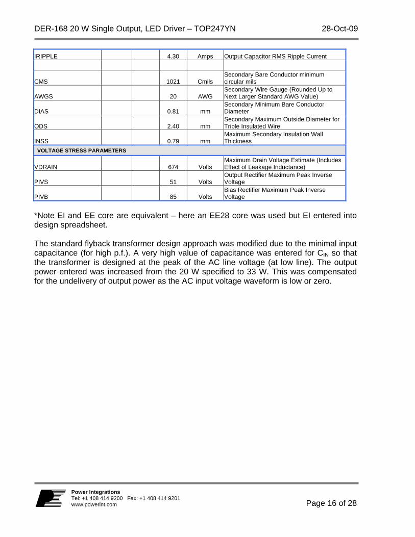
*Note EI and EE core are equivalent – here an EE28 core was used but EI entered into design spreadsheet. The standard flyback transformer design approach was modified due to the minimal input capacitance (for high p.f.). A very high value of capacitance was entered for CIN so that the transformer is designed at the peak of the AC line voltage (at low line). The output power entered was increased from the 20 W specified to 33 W. This was compensated for the undelivery of output power as the AC input voltage waveform is low or zero.
28-Oct-09 DER-168 20 W Single Output, LED Driver – TOP247YN
Page 17 of 28
Power Integrations Tel: +1 408 414 9200 Fax: +1 408 414 9201
www.powerint.com
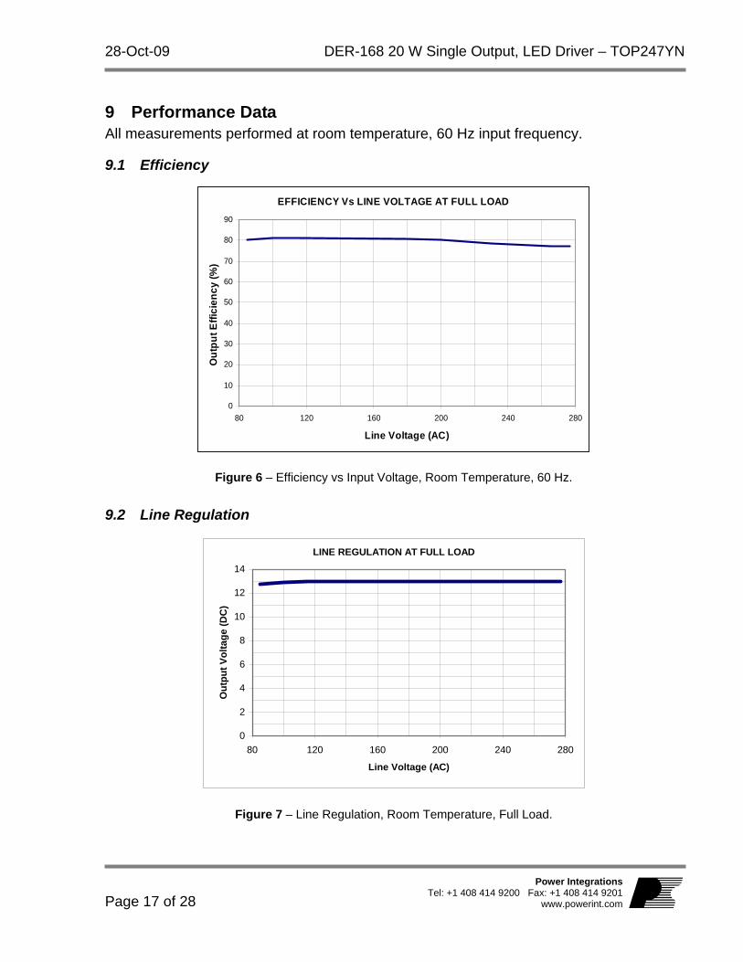
9 Performance Data All measurements performed at room temperature, 60 Hz input frequency.
9.1 Efficiency
EFFICIENCY Vs LINE VOLTAGE AT FULL LOAD
0
10
20
30
40
50
60
70
80
90
80 120 160 200 240 280
Line Voltage (AC)
Ou
tpu
t E
ffic
ien
cy
(%
)
Figure 6 – Efficiency vs Input Voltage, Room Temperature, 60 Hz.
9.2 Line Regulation
LINE REGULATION AT FULL LOAD
0
2
4
6
8
10
12
14
80 120 160 200 240 280
Line Voltage (AC)
Ou
tpu
t V
olt
ag
e (
DC
)
Figure 7 – Line Regulation, Room Temperature, Full Load.

DER-168 20 W Single Output, LED Driver – TOP247YN 28-Oct-09
Page 18 of 28
Power Integrations Tel: +1 408 414 9200 Fax: +1 408 414 9201 www.powerint.com
9.3 Harmonic Content
Input Current Harmonic Content
0
50
100
150
200
250
1 2 3 4 5 6 7 8 9 10
Harmonic
Inp
ut
Cu
rre
nt
(mA
)
115VAC
230VAC
Figure 8 – Input Current Harmonic Content at Full Load.
9.4 Harmonic Content in Percentage of Fundamental
Harmonic 115 AC Iin(mA)
% of Fundamental
Maximum % Allowed By IEC 61000-3-2
230 AC Iin(mA)
% of Fundamental
Maximum % Allowed By IEC 61000-3-2. Class C
1 234 139
2 3.2 1.37 2 0.9 0.65 2
3 2.9 1.24 29.7 11 7.91 28.0
4 2.6 1.11 0.6 0.43
5 3.6 1.54 10 6.1 4.39 10
6 0.8 0.34 1.5 1.08
7 6.9 2.95 7 8.5 6.12 7
8 1.6 0.68 1.6 1.15
9 7.6 3.25 5 7.8 5.61 5
10 1.3 0.56 0.9 0.65
Figure 9 – Harmonic Content in Percentage of Fundamental and IEC 61000-3-2 Limits for C Class Equipment. NOTE: Third Harmonic Spec Follows the Formula: 30* PFC. (Power Factor at 115/230 VAC).

28-Oct-09 DER-168 20 W Single Output, LED Driver – TOP247YN
Page 19 of 28
Power Integrations Tel: +1 408 414 9200 Fax: +1 408 414 9201
www.powerint.com
9.5 Power Factor Vs Line Voltage at Full Load
Vin PF 85 0.970
115 0.990 230 0.934 277 0.902
Figure 10 – Power Factor (PF) vs Input Line Voltage (VAC).
Power Factor Vs Line Voltage
0.89
0.9
0.91
0.92
0.93
0.94
0.95
0.96
0.97
0.98
0.99
1
50 100 150 200 250 300
Line Voltage (VAC)
Po
wer
Fac
tor
(PF
)

DER-168 20 W Single Output, LED Driver – TOP247YN 28-Oct-09
Page 20 of 28
Power Integrations Tel: +1 408 414 9200 Fax: +1 408 414 9201 www.powerint.com
10 Thermal Performance Thermal data were taken with unit inside a closed cardboard box at room temperature.
Temperature (C) Item
85 VAC 277 VAC
Ambient Outside the Box
25 25
TOPSWITCH (U1) 42 53
Transformer (T1) 46 52
Output Rectifiers (D10, D11)
58 60
28-Oct-09 DER-168 20 W Single Output, LED Driver – TOP247YN
Page 21 of 28
Power Integrations Tel: +1 408 414 9200 Fax: +1 408 414 9201
www.powerint.com
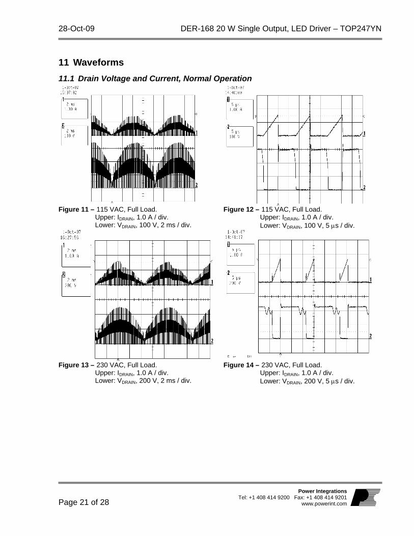
11 Waveforms
11.1 Drain Voltage and Current, Normal Operation
Figure 11 – 115 VAC, Full Load.
Upper: IDRAIN, 1.0 A / div. Lower: VDRAIN, 100 V, 2 ms / div.
Figure 12 – 115 VAC, Full Load. Upper: IDRAIN, 1.0 A / div. Lower: VDRAIN, 100 V, 5 s / div.
Figure 13 – 230 VAC, Full Load. Upper: IDRAIN, 1.0 A / div. Lower: VDRAIN, 200 V, 2 ms / div.
Figure 14 – 230 VAC, Full Load. Upper: IDRAIN, 1.0 A / div. Lower: VDRAIN, 200 V, 5 s / div.

DER-168 20 W Single Output, LED Driver – TOP247YN 28-Oct-09
Page 22 of 28
Power Integrations Tel: +1 408 414 9200 Fax: +1 408 414 9201 www.powerint.com
11.2 Output Voltage Start-up Profile
Figure 15 – Start-up Profile, 115 VAC 2 V, 50 ms / div.
Figure 16 – Start-up Profile, 230 VAC 2 V, 50 ms / div.
11.3 Drain Voltage and Current Start-up Profile
Figure 17 – 115 VAC Input and Maximum Load.
Upper: IDRAIN Lower: VDRAIN
Figure 18 – 230 VAC Input and Maximum Load. Upper: IDRAIN Lower: VDRAIN

28-Oct-09 DER-168 20 W Single Output, LED Driver – TOP247YN
Page 23 of 28
Power Integrations Tel: +1 408 414 9200 Fax: +1 408 414 9201
www.powerint.com
11.4 Output Ripple Measurements
11.4.1 Ripple Measurement Technique
For DC output ripple measurements, a modified oscilloscope test probe must be utilized in order to reduce spurious signals due to pickup. Details of the probe modification are provided in the figures below. The 4987BA probe adapter is affixed with two capacitors tied in parallel across the probe tip. The capacitors include one (1) 0.1 F/50 V ceramic type and one (1) 1.0 F/50 V aluminum electrolytic. The aluminum electrolytic type capacitor is polarized, so proper polarity across DC outputs must be maintained (see below).
Figure 19 – Oscilloscope Probe Prepared for Ripple Measurement. (End Cap and Ground Lead
Removed).
Figure 20 – Oscilloscope Probe with Probe Master (www.probemaster.com) 4987A BNC Adapter.
(Modified with wires for ripple measurement, and two parallel decoupling capacitors added).
Probe Ground
Probe Tip

DER-168 20 W Single Output, LED Driver – TOP247YN 28-Oct-09
Page 24 of 28
Power Integrations Tel: +1 408 414 9200 Fax: +1 408 414 9201 www.powerint.com
11.4.2 Measurement Results
AC coupled measurements showing 1.5 VP-P output ripple at 120 HZ.
Figure 21 – Ripple, 115 VAC, Full Load.
5 ms, 1 V / div. Figure 22 – Ripple, 230 VAC, Full Load.
5 ms, 1 V /div.

28-Oct-09 DER-168 20 W Single Output, LED Driver – TOP247YN
Page 25 of 28
Power Integrations Tel: +1 408 414 9200 Fax: +1 408 414 9201
www.powerint.com
12 Surge Test
12.1 Surge Test Results with 1.2/50us Waveform
Surge Level (V)
Input Voltage (VAC)
Injection Location
Injection Phase (°)
Number Of Surges
Test Result (Pass/Fail)
+500 230 L to N 90 10 Pass -500 230 L to N 90 10 Pass
+1000 230 L and N to G 90 10 Pass -1000 230 L and N to G 90 10 Pass
12.2 Surge Test Results with 0.5us-100 kHz Ring-Waveform
Surge Level (V)
Input Voltage (VAC)
Injection Location
Injection Phase (°)
Number Of Surges
Test Result (Pass/Fail)
+2500 230 L to N 90 10 Pass -2500 230 L to N 90 10 Pass +2500 230 L and N to G 90 10 Pass -2500 230 L and N to G 90 10 Pass

DER-168 20 W Single Output, LED Driver – TOP247YN 28-Oct-09
Page 26 of 28
Power Integrations Tel: +1 408 414 9200 Fax: +1 408 414 9201 www.powerint.com
13 Conducted EMI
Figure 23 – Conducted EMI, 115 VAC Full Load, LIGHT Traces: N, BOLD Traces: L. OUTRET Grounded.
Figure 24 – Conducted EMI, 230 VAC. Full Load, LIGHT Traces: N, BOLD Traces L. OUTRET Grounded.

28-Oct-09 DER-168 20 W Single Output, LED Driver – TOP247YN
Page 27 of 28
Power Integrations Tel: +1 408 414 9200 Fax: +1 408 414 9201
www.powerint.com
14 Revision History
Date Author Revision Description & changes Reviewed 19-Nov-07 SGK 1.0 Initial Release 18-Dec-07 SGK 1.1 Corrected Schematic 28-Oct-09 VC 1.2 Correct BOM and schematic
to eliminate temp parts

DER-168 20 W Single Output, LED Driver – TOP247YN 28-Oct-09
Page 28 of 28
Power Integrations Tel: +1 408 414 9200 Fax: +1 408 414 9201 www.powerint.com
For the latest updates, visit our website: www.powerint.com Power Integrations reserves the right to make changes to its products at any time to improve reliability or manufacturability. Power Integrations does not assume any liability arising from the use of any device or circuit described herein. POWER INTEGRATIONS MAKES NO WARRANTY HEREIN AND SPECIFICALLY DISCLAIMS ALL WARRANTIES INCLUDING, WITHOUT LIMITATION, THE IMPLIED WARRANTIES OF MERCHANTABILITY, FITNESS FOR A PARTICULAR PURPOSE, AND NON-INFRINGEMENT OF THIRD PARTY RIGHTS.
PATENT INFORMATION The products and applications illustrated herein (including transformer construction and circuits external to the products) may be covered by one or more U.S. and foreign patents, or potentially by pending U.S. and foreign patent applications assigned to Power Integrations. A complete list of Power Integrations’ patents may be found at www.powerint.com. Power Integrations grants its customers a license under certain patent rights as set forth at http://www.powerint.com/ip.htm. The PI Logo, TOPSwitch, TinySwitch, LinkSwitch, DPA-Switch, PeakSwitch, EcoSmart, Clampless, E-Shield, Filterfuse, StackFET, PI Expert and PI FACTS are trademarks of Power Integrations, Inc. Other trademarks are property of their respective companies. ©Copyright 2009 Power Integrations, Inc.
Power Integrations Worldwide Sales Support Locations
WORLD HEADQUARTERS 5245 Hellyer Avenue San Jose, CA 95138, USA. Main: +1-408-414-9200 Customer Service: Phone: +1-408-414-9665 Fax: +1-408-414-9765 e-mail: [email protected]
GERMANY Rueckertstrasse 3 D-80336, Munich Germany Phone: +49-89-5527-3911 Fax: +49-89-5527-3920 e-mail: [email protected]
JAPAN Kosei Dai-3 Building 2-12-11, Shin-Yokohama, Kohoku-ku, Yokohama-shi, Kanagawa 222-0033 Japan Phone: +81-45-471-1021 Fax: +81-45-471-3717 e-mail: [email protected]
TAIWAN 5F, No. 318, Nei Hu Rd., Sec. 1 Nei Hu District Taipei 114, Taiwan R.O.C. Phone: +886-2-2659-4570 Fax: +886-2-2659-4550 e-mail: [email protected]
CHINA (SHANGHAI) Rm 1601/1610, Tower 1 Kerry Everbright City No. 218 Tianmu Road West Shanghai, P.R.C. 200070 Phone: +86-021-6354-6323 Fax: +86-021-6354-6325 e-mail: [email protected]
INDIA #1, 14th Main Road Vasanthanagar Bangalore-560052 India Phone: +91-80-4113-8020 Fax: +91-80-4113-8023 e-mail: [email protected]
KOREA RM 602, 6FL Korea City Air Terminal B/D, 159-6 Samsung-Dong, Kangnam-Gu, Seoul, 135-728 Korea Phone: +82-2-2016-6610 Fax: +82-2-2016-6630 e-mail: [email protected]
UNITED KINGDOM 1st Floor, St. James’s House East Street, Farnham Surrey, GU9 7TJ United Kingdom Phone: +44 (0) 1252-730-141 Fax: +44 (0) 1252-727-689 e-mail: [email protected]
CHINA (SHENZHEN) Rm A, B & C 4th Floor, Block C, Electronics Science and Technology Building 2070 Shennan Zhong Road Shenzhen, Guangdong, P.R.C. 518031 Phone: +86-755-8379-3243 Fax: +86-755-8379-5828 e-mail: [email protected]
ITALY Via De Amicis 2 20091 Bresso MI Italy Phone: +39-028-928-6000 Fax: +39-028-928-6009 e-mail: [email protected]
SINGAPORE 51 Newton Road, #15-08/10 Goldhill Plaza Singapore, 308900 Phone: +65-6358-2160 Fax: +65-6358-2015 e-mail: [email protected]
APPLICATIONS HOTLINE World Wide +1-408-414-9660 APPLICATIONS FAX World Wide +1-408-414-9760