design, fabrication, and characterization of pseudomorphic
TRANSCRIPT
University of South CarolinaScholar Commons
Theses and Dissertations
2015
Design, Fabrication, and Characterization ofPseudomorphic and Quasi-PseudomorphicAlGaN Based Deep Ultraviolet Light EmittingDiodes Over SapphireFatima AsifUniversity of South Carolina - Columbia
Follow this and additional works at: https://scholarcommons.sc.edu/etd
Part of the Electrical and Computer Engineering Commons
This Open Access Dissertation is brought to you by Scholar Commons. It has been accepted for inclusion in Theses and Dissertations by an authorizedadministrator of Scholar Commons. For more information, please contact [email protected].
Recommended CitationAsif, F.(2015). Design, Fabrication, and Characterization of Pseudomorphic and Quasi-Pseudomorphic AlGaN Based Deep Ultraviolet LightEmitting Diodes Over Sapphire. (Doctoral dissertation). Retrieved from https://scholarcommons.sc.edu/etd/3140

Design, Fabrication, and Characterization of Pseudomorphic andQuasi-Pseudomorphic AlGaN Based Deep Ultraviolet Light Emitting
Diodes Over Sapphire
by
Fatima Asif
Bachelor of ScienceUniversity of Engineering and Technology, Lahore 2003
Master of ScienceUniversity of South Carolina 2011
Submitted in Partial Fulfillment of the Requirements
for the Degree of Doctor of Philosophy in
Electrical Engineering
College of Engineering and Computing
University of South Carolina
2015
Accepted by:
Asif Khan, Major Professor
Mohammod Ali, Committee Member
Enrico Santi, Committee Member
Jamil Khan, Committee Member
Lacy Ford, Vice Provost and Dean of Graduate Studies

© Copyright by Fatima Asif, 2015All Rights Reserved.
ii
Dedication
Dedicated to my loving family.
iii
Acknowledgments
I would like to express my sincere gratitude to my advisor, Professor Asif Khan, from
whom I have learned so much, about life and research. He has been a true inspiration,
and I thank him for his guidance in helping me develop into a better researcher and
human being. Next, I would like to thank the members of my dissertation committee:
Prof. Enrico Santi, Prof. Jamil Khan, and Prof. Mohammod Ali, for their many
insightful comments and suggestions that have helped improve this dissertation. I
would also like to acknowledge and thank Nitek, Inc. for their collaboration and help
in this research. This research is the outcome of a team effort and would not have
succeeded without the help of many kind and brilliant researchers. I would especially
like to thank Dr. Vinod Adivarahan, Dr. Mohamed Lachab, Dr. Iftikhar Ahmed,
Dr. Qhalid Fareed, Bin Zhang, and Dr. Alex Lunev from Nitek. I wish to thank
my fellow colleagues and researchers over the years, Ahmad Heidari, Dr. Monirul
Islam, Dr. Seongmo Hwang, Dr. Joe Dion, Dr. Hung-Chi Chen, Sho Sugiyama,
Mahbuba Sultana, Sakib Muhtadi, Antwon Coleman, Morgan Gauthreaus, Daniel
Morgan, Josh Raiborde, Blythe Johnson, and many others, for their friendship, help,
and camaraderie. I would also like to thank the friendly staff at department of
electrical engineering including Nat Paterson, Ashley Burt, Heather Covey, and Alicia
Williams. Most importantly, I wish to thank my family: my parents, my husband,
my brothers and sisters, for loving me, for believing in me, and for supporting me
every step of the way.
iv
Abstract
III-Nitride based deep ultraviolet (UV) light emitting diodes (LEDs) emitting below
280nm has the potential to replace mercury lamps currently used in the systems for
water/air purification, germicidal and medical instruments sterilization applications.
However, this potential has not yet been fully realized as the output power, quantum
efficiency and lifetime of deep UV-LEDs have been limited by the large number of
dislocations in the active region of the devices, arising from the lattice mismatched
sapphire substrate, which has been the substrate of choice due to its high transparency
to deep UV radiation. To reduce dislocations in the active region of the DUV LEDs
grown on sapphire, AlN/AlGaN short period superlattice is usually grown to manage
strain and filter the dislocations. However, the growth of these thick superlattice is
not only time consuming but it can also cause severe substrate bowing making device
fabrication a challenge. An alternative method for reducing the dislocation density
in deep UV-LEDs structure is the use of low defect density bulk AlN substrates,
which has more than two orders of magnitude low defect density than sapphire/AlN
template. In spite of such a lower density of defects, the quantum efficiency values for
DUV LEDs on bulk AlN substrate are very similar to that of DUV LEDs on sapphire.
This is due to the high absorption coefficient of AlN substrate in the deep UV region;
also the high cost and limited availability are important issues. This dissertation
focuses on the design, fabrication and characterization of Deep UV LEDs employing
the pseudomorphic structure similar to those grown on bulk AlN, in order to keep
the active layers crystalline quality very close to that of the underlying AlN/Sapphire
template. Other LED designs, with different degree of relaxation of the n-AlGaN
v
current spreading layer were also investigated with the main target of achieving a
cost-effective design without compromising the resulting device performance, namely
output power and reliability.
vi
Table of ContentsDedication . . . . . . . . . . . . . . . . . . . . . . . . . . . . . . . . . . iii
Acknowledgments . . . . . . . . . . . . . . . . . . . . . . . . . . . . . iv
Abstract . . . . . . . . . . . . . . . . . . . . . . . . . . . . . . . . . . . v
List of Figures . . . . . . . . . . . . . . . . . . . . . . . . . . . . . . . ix
Chapter 1 Introduction . . . . . . . . . . . . . . . . . . . . . . . . . 1
1.1 Applications of Ultraviolet Light Emitting Diodes . . . . . . . . . . . 2
1.2 History of III-Nitride Light Emitting Diodes . . . . . . . . . . . . . . 6
1.3 Quantum Efficiency of III-Nitride Light Emitting Diodes . . . . . . . 8
1.4 Review of III-Nitride Deep Ultraviolet Light Emitting Diodes . . . . 12
Chapter 2 Problem Identification and Characterization Tech-niques . . . . . . . . . . . . . . . . . . . . . . . . . . . . . 17
2.1 Problem Identification . . . . . . . . . . . . . . . . . . . . . . . . . . 17
2.2 Material Characterization . . . . . . . . . . . . . . . . . . . . . . . . 20
2.3 Device Characterization . . . . . . . . . . . . . . . . . . . . . . . . . 28
Chapter 3 Pseudomorphic Deep Ultraviolet Light EmittingDiodes over Sapphire . . . . . . . . . . . . . . . . . . . . 31
3.1 Investigation of Epilayer Quality Using Optical-Pumping . . . . . . . 33
3.2 Development of Pseudomorphic Deep Ultraviolet Light EmittingDiodes . . . . . . . . . . . . . . . . . . . . . . . . . . . . . . . . . . 44
vii
Chapter 4 Quasi-Pseudomorphic Deep Ultraviolet Light Emit-ting Diodes over Sapphire . . . . . . . . . . . . . . . . 54
4.1 Epilayer Structure . . . . . . . . . . . . . . . . . . . . . . . . . . . . 55
4.2 Material Characterization . . . . . . . . . . . . . . . . . . . . . . . . 56
4.3 Device Processing . . . . . . . . . . . . . . . . . . . . . . . . . . . . . 59
4.4 Electrical and Optical Characterization of Devices . . . . . . . . . . . 59
Chapter 5 Selective Area Deposition for Deep UltravioletLight Emitting Diodes over Sapphire . . . . . . . . . . 68
5.1 The Effects of n-AlGaN Thickness on Device Performance . . . . . . 69
5.2 Selective Area Deposition of n-AlGaN and MQW Structure . . . . . 72
Chapter 6 Conclusions and Future Work . . . . . . . . . . . . . 78
6.1 Conclusions . . . . . . . . . . . . . . . . . . . . . . . . . . . . . . . . 78
6.2 Future Work . . . . . . . . . . . . . . . . . . . . . . . . . . . . . . . 80
Bibliography . . . . . . . . . . . . . . . . . . . . . . . . . . . . . . . . 82
Appendix A Permission to Reprint . . . . . . . . . . . . . . . . . . . 98
viii

List of FiguresFigure 1.1 The UV radiation damages the DNA of microorganisms [3]. . . . 3
Figure 1.2 Depiction of NLOS deep UV communication. . . . . . . . . . . . 5
Figure 1.3 Features of UV-LEDs in comparison with mercury UV lamps [11]. 6
Figure 1.4 Band diagram for GaN/InGaN LED with electron blockinglayer [39]. . . . . . . . . . . . . . . . . . . . . . . . . . . . . . . . 9
Figure 1.5 Band diagram illustrating non-radiative recombination (a) viadefects/traps, (b) via auger processes and (c) radiative recom-bination via band-to-band recombination [39]. . . . . . . . . . . . 10
Figure 1.6 Diagram illustrating the effect of refractive index mismatch onlight extraction. . . . . . . . . . . . . . . . . . . . . . . . . . . . . 11
Figure 1.7 State-of-the-art in EQE for near UV and DUV-LEDs [50]. . . . . 13
Figure 1.8 Simulated internal quantum efficiency versus the dislocationdensity for 280 nm DUV-LEDs. . . . . . . . . . . . . . . . . . . . 14
Figure 2.1 A typical schematic of DUV-LEDs [73]. . . . . . . . . . . . . . . . 18
Figure 2.2 Sheet resistance mapping of n-AlGaN layer with average sheetresistance of 105 Ω/sq. . . . . . . . . . . . . . . . . . . . . . . . . 21
Figure 2.3 AFM in tapping mode [80]. . . . . . . . . . . . . . . . . . . . . . 23
Figure 2.4 The Van der Waals forces regime versus distance. . . . . . . . . . 24
Figure 2.5 An AFM image of AlN/sapphire template after etching withEPD of 3x108 cm-2. . . . . . . . . . . . . . . . . . . . . . . . . . . 25
Figure 2.6 Different schemes of X-Ray diffractometers [83]. . . . . . . . . . . 26
Figure 2.7 Mechanism of X-Ray diffraction. . . . . . . . . . . . . . . . . . . 27
Figure 2.8 Reciprocal space mapping showing fully strained AlGaN layer. . . 28
ix

Figure 3.1 Schematic representation of the optically pumped AlGaN/AlGaNMQW structure grown on sapphire substrate. . . . . . . . . . . . 36
Figure 3.2 Schematic diagram of the setup used for optical pumping ex-periments. . . . . . . . . . . . . . . . . . . . . . . . . . . . . . . . 36
Figure 3.3 Calculated distribution of the optical mode amplitude. . . . . . . 37
Figure 3.4 RSM of the asymmetric (105) reflection for the photo-pumpedAlGaN MQW structure showing a partially relaxed n-AlGaNmaterial with respect to the underlying AlN buffer layer. . . . . . 38
Figure 3.5 Edge PL spectra from the partially relaxed AlGaN/AlGaNMQWsmeasured at room temperature for different pump power den-sities. . . . . . . . . . . . . . . . . . . . . . . . . . . . . . . . . . 39
Figure 3.6 Plot of the integrated edge PL intensity (a) and both emissionpeak wavelength and line-width (b) as a function of the excita-tion source power density for a laser bar with a CL = 2.3 mm.The inset shows optically resolved PL emission measured justaround the threshold. . . . . . . . . . . . . . . . . . . . . . . . . . 40
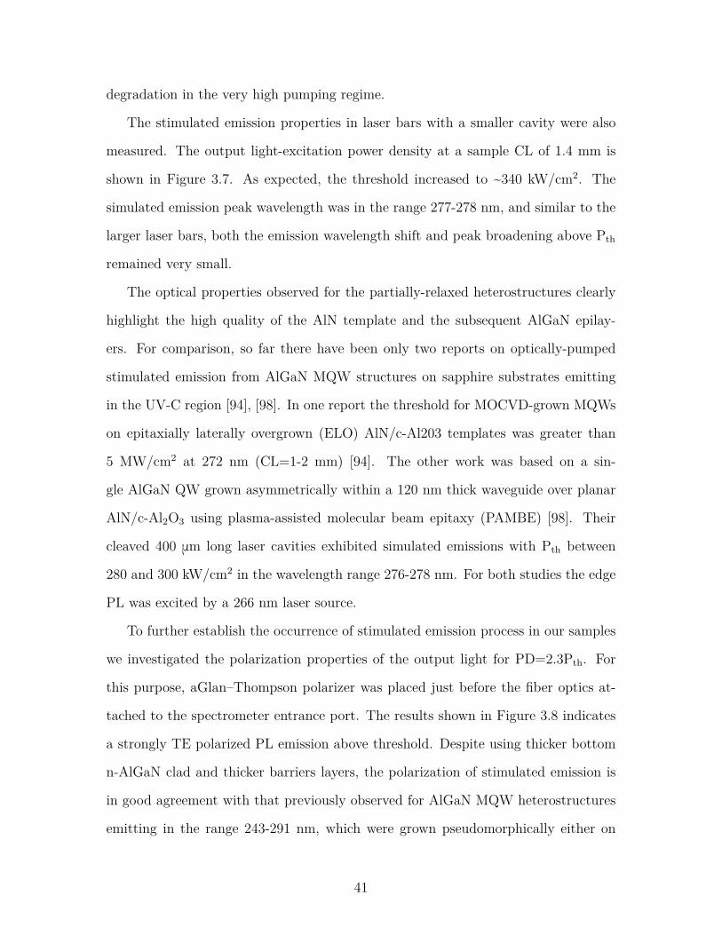
Figure 3.7 Output light intensity and emission line-width plotted vs theoptical pump power density for a laser bar with a 1.4mm cavitylength. The inset shows a PL spectrum measured for PD =1.09 MW/cm2. . . . . . . . . . . . . . . . . . . . . . . . . . . . . 42
Figure 3.8 TE and TM mode edge PL spectra measured for the 276 nmMQW structure above the threshold power density (PD = 588kW/cm2). . . . . . . . . . . . . . . . . . . . . . . . . . . . . . . . 43
Figure 3.9 n-AlGaN sheet resistance for (a) standard SPSL LED, (b) pseu-domorphic LED with standard doping and (c) pseudomorphicLED with PMD. . . . . . . . . . . . . . . . . . . . . . . . . . . . 45
Figure 3.10 Study of Etch pit Density (EPD) after KOH etching for n-AlGaN with standard doping (a), and n-AlGaN with PMD dop-ing (b). . . . . . . . . . . . . . . . . . . . . . . . . . . . . . . . . 46
Figure 3.11 XRD reciprocal space mapping of pseudomorphic (a) and stan-dard SPSL (b) DUV-LED structures. . . . . . . . . . . . . . . . . 47
Figure 3.12 Schematics of the DUV-LED epilayer structures: standard SPSL(relaxed) LED (left) and pseudomorphic LED (right). . . . . . . 48
x
Figure 3.13 EL spectrum of pseudomorphic LED measured in dc mode. . . . . 49
Figure 3.14 I-V characteristics of pseudomorphic and standard SPSL LEDsmeasured in dc mode. The inset represents SEM image of thepixel-LED device with 360 x 360 μm2 p-active area. . . . . . . . . 50
Figure 3.15 L-I characteristics measured in dc mode for pseudomorphic andstandard SPSL LEDs with 360 x 360 μm2 emission areas. . . . . . 51
Figure 3.16 lifetime testing data for packaged pseudomorphic LEDs at RTwith different packaging schemes. For comparison, reliability ofa reference standard SPSL LED was also measured. . . . . . . . 52
Figure 4.1 Schematic diagram of DUV-LED epilayer structures: standardSPSL LED (a) and Quasi-pseudomorphic LED (b). . . . . . . . . 55
Figure 4.2 Sheet resistance mapping of Standard SPSL LED (a) and Quasi-pseudomorphic LED (b). . . . . . . . . . . . . . . . . . . . . . . . 57
Figure 4.3 XRD reciprocal space mapping of quasi-pseudomorphic LEDs(a) and Standard SPSL LEDs (b). . . . . . . . . . . . . . . . . . 58
Figure 4.4 RT normalized EL spectra of Quasi-pseudomorphic and stan-dard SPSL DUV-LEDs measured at 20mA pump current. . . . . 60
Figure 4.5 I-V characteristics of standard SPSL and quasi-pseudomorphicLEDs measured in dc mode. . . . . . . . . . . . . . . . . . . . . . 61
Figure 4.6 The plot of dc output power as a function of pump currentfor standard SPSL and quasi-pseudomorphic packaged LEDsmeasured at RT. . . . . . . . . . . . . . . . . . . . . . . . . . . . 62
Figure 4.7 The ratio of standard SPSL LEDs output power over the quasi-pseudomorphic LEDs as a function of pump currents. . . . . . . . 63
Figure 4.8 External quantum efficiency (EQE) for quasi-pseudomorphicand standard SPSL LEDs under dc pump currents. . . . . . . . . 65
Figure 4.9 Reliability comparison of quasi-pseudomorphic versus standardSPSL LEDs, at room temperature, packaged on TO-3 headers. . . 66
Figure 5.1 Schematic diagram of DUV-LEDs with different n-AlGaN thickness. 69
xi

Figure 5.2 n-AlGaN Sheet resistance for (a) device A (b) device B and (c)device C.. . . . . . . . . . . . . . . . . . . . . . . . . . . . . . . . 70
Figure 5.3 devices I-V characteristics measured at RT. . . . . . . . . . . . . 71
Figure 5.4 RT current- output Power (I-L) characteristics of the devicesmeasured in dc mode. . . . . . . . . . . . . . . . . . . . . . . . . 72
Figure 5.5 Schematic diagram of standard SPSL (left) and SAD (right) LEDs. 73
Figure 5.6 Process-flow for selective area deposition (SAD) approach . . . . 74
Figure 5.7 AFM image of SAD n-AlGaN. . . . . . . . . . . . . . . . . . . . . 74
Figure 5.8 EL spectrum of SAD LEDs . . . . . . . . . . . . . . . . . . . . . 75
Figure 5.9 I-V characteristics for unetched SAD samples versus etchedsamples with different metal schemes. . . . . . . . . . . . . . . . . 76
xii

Chapter 1
Introduction
After decades of technological advancements and reduction in manufacturing costs,
semiconductor fabrication technologies are finally in a position to replace the tra-
ditional incandescent light bulb. Light emitting diodes (LED) are emerging as the
technology of choice in a wide range of applications, including but not limited to
residential and commercial illumination, solid-state displays, non-line-of-sight com-
munication, automotive lighting, and biomedical sterilization. The current generation
of LEDs have higher tolerance to shock, temperature and humidity, have higher effi-
ciencies, longer life spans, and much lower environmental impact than fluorescent or
incandescent light sources.
Due to the large number of applications, a greater research focus has been placed
on LEDs with light emission in the visible light spectrum. However, a number of
technologically important applications require LEDs with shorter wavelength emis-
sions in the ultraviolet (UV) range. Ultraviolet Light emitting diodes (UVLED) emit
light in the UV region of electromagnetic spectrum with wavelengths ranging from
10-400 nm. Deep UV LEDs (DUV-LED) have light emissions with wavelengths in the
200-290 nm range. The primary focus of this research is on the design, fabrication,
and characterization of DUV-LEDs particularly those based on pseudomorphic and
quasi-pseudomorphic growth of Aluminum-Gallium-Nitride (AlGaN) epilayers over
sapphire.
This introductory chapter starts with a brief introduction to the applications of
DUV-LEDs. Section 1.2 presents LEDs based on group III-nitrides which include
1
the AlGaN-based LEDs. Section 1.3 describes the injection, extraction, and internal
quantum efficiencies of these LEDs and introduces the different parameters that have
been used to quantify these efficiencies. A brief survey of research literature capturing
the evolution of the design of DUV-LEDs is presented in Section 1.4.
Chapter 2 introduces the established techniques and terminologies used to char-
acterize these materials and devices. The underlying issues responsible for the low
optical output power and low quantum efficiency of DUV-LEDs are also discussed
in this chapter. Chapter 3 begins with an analysis of AlGaN based multiple quan-
tum wells (MQW) quality using photo-pumping and presents the fabrication process
and characterization schemes for pseudomorphic DUV-LEDs. Chapter 4 describes
the development of quasi-pseudomorphic LEDs and provide a detailed comparison
with pseudomorphic and standard SPSL LEDs with superlattice structure. A novel
approach based on selective area material deposition is proposed in Chapter 5, along
with the preliminary results. Chapter 6 concludes the dissertation with a detailed
discussion of the outcomes of various experiments and the conclusions derived from
them.
1.1 Applications of Ultraviolet Light Emitting Diodes
Ultraviolet Light emitting diodes emit light in the UV region of electromagnetic
spectrum. UV radiations can be further subdivided into four distinct regions: UV-A
(320–400 nm); UV-B (290-320 nm); UV-C or deep UV (200-290 nm); and vacuum
UV (10-200 nm) [1].
UV LEDs have been used in a wide range of applications that take advantage of
uniques characteristics of these electromagnetic radiations. Devices with emission in
the UV-A range, particularly with wavelengths in 365-375 nm range, are generally
used in low-power applications such as photo-catalytic deodorizing units in air con-
ditioners and refrigerators. These devices range in power between 3-10 mW. UV-A
2
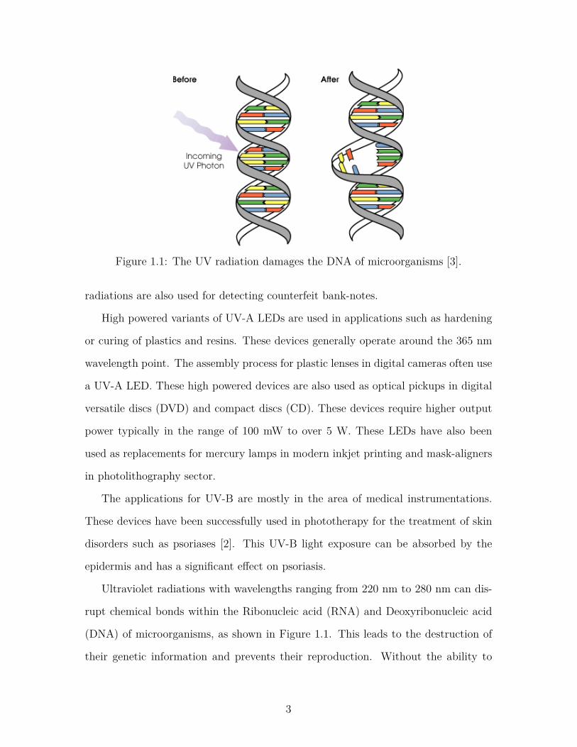
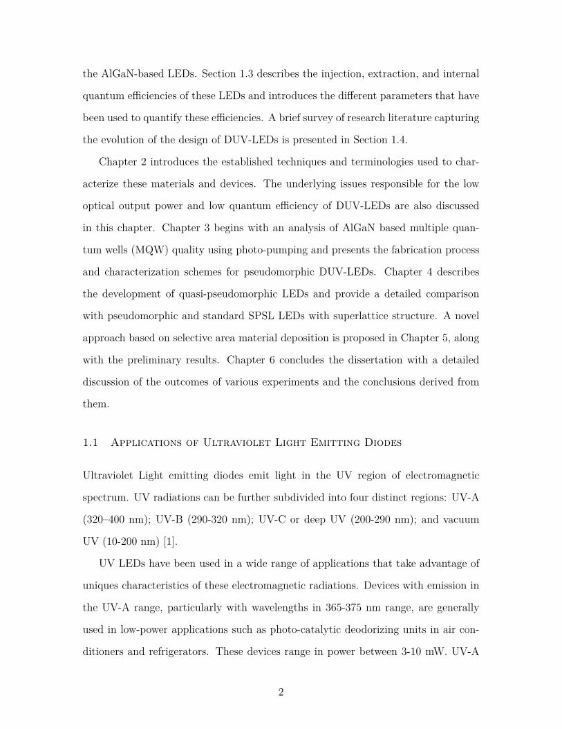
Figure 1.1: The UV radiation damages the DNA of microorganisms [3].
radiations are also used for detecting counterfeit bank-notes.
High powered variants of UV-A LEDs are used in applications such as hardening
or curing of plastics and resins. These devices generally operate around the 365 nm
wavelength point. The assembly process for plastic lenses in digital cameras often use
a UV-A LED. These high powered devices are also used as optical pickups in digital
versatile discs (DVD) and compact discs (CD). These devices require higher output
power typically in the range of 100 mW to over 5 W. These LEDs have also been
used as replacements for mercury lamps in modern inkjet printing and mask-aligners
in photolithography sector.
The applications for UV-B are mostly in the area of medical instrumentations.
These devices have been successfully used in phototherapy for the treatment of skin
disorders such as psoriases [2]. This UV-B light exposure can be absorbed by the
epidermis and has a significant effect on psoriasis.
Ultraviolet radiations with wavelengths ranging from 220 nm to 280 nm can dis-
rupt chemical bonds within the Ribonucleic acid (RNA) and Deoxyribonucleic acid
(DNA) of microorganisms, as shown in Figure 1.1. This leads to the destruction of
their genetic information and prevents their reproduction. Without the ability to
3

reproduce, these microorganisms are rendered harmless when consumed by humans
[4]. Hence, the primary applications for UV-C emitters are in the area of air/water
purification and surface sterilization.
In water purification systems, the water is irradiated with UV light to clear bac-
terias and viruses. The peak absorbance of these radiations by DNA takes place at
approximately 260 nm. However, the optimal wavelength for disinfection varies with
the target microorganism. For the eradication of pathogens such as E-coli in water,
the optimal wavelength for radiations is reported to be 269 nm [5]. UV LED based
water purification systems have already been demonstrated for standing and running
water [6], [7].
The III-nitride-based DUV-LEDs have also been used in defense applications,
such as non-line-of-sight (NLOS) communication and bio-agent detection. NLOS
communication utilizes the spectrum with wavelengths shorter than 280 nm. This
frequency range has also been called as the solar blind region since the radiations in
this region are absorbed by the ozone layer. This property leads to a dual benefits
for NLOS communication. The absorption of extra-terrestrial radiations results to
low background noise in this frequency range[8]. Hence, a higher signal to noise
ratio allows for easy signal detection. Due to high absorption, the signal cannot
be detected from a distance, allowing for covert communications. Furthermore, the
UV light generated near earth’s surface are strongly scattered by atmospheric gases.
This scattering facilitate the signal to be transmitted without direct line of sight
restrictions. The system would consist of a transmitter unit with a UV source (λ<280
nm) and a receiver with a solar-blind detector, as shown in Figure 1.2. The receiver
would be able to detect a signal from the transmitter as long as the distance between
them is between 10 and 250 meters.
The deep UV-C region of the spectrum is also ideal for detection of the fluorescence
of chemical compounds in bacteria present in the environment. The unknown agent
4

Figure 1.2: Depiction of NLOS deep UV communication.
is illuminated by the UV light source, and the emitted fluorescence spectrum can
then be used to identify the presence of certain dangerous biological agents [9].
The combined market for UV LEDs is fairly large. The water purification market
alone is estimated to be worth more than $5 billion [10]. With rapid technological
advancement, UV LEDs are poised to replace the traditional UV mercury lamps in a
large number of applications. UV mercury lamps are bulky, fragile, environmentally
hazardous, have lower life spans, require regular maintenance and high voltage to
operate. With fast turn on/off speeds, small footprint, low voltage operation and the
ability to operate in cold environments, UV-LEDs based on III-nitrides offer many
advantages over traditional mercury lamps as shown in Figure 1.3.
Different applications may require a light source with light emissions at varying
wavelengths. Consequently, it is essential to fabricate an optoelectronic device with
emission frequencies that can be tailored to the requirements of different applications.
A ternary alloy between Gallium Nitride (GaN) and Aluminum Nitride (AlN) can
be tuned to emit light at every wavelength across the ultraviolet spectrum. These
devices are part of a larger family of light emitting diodes, known as the III-nitride
LEDs, introduced in the next section.
5
Figure 1.3: Features of UV-LEDs in comparison with mercury UV lamps [11].
1.2 History of III-Nitride Light Emitting Diodes
The III-nitride material system has direct band gap, making it an ideal candidate for
the development of optoelectronic devices. The wide band gap of this material system
allows us to tune the band gap energies from 0.7 eV for Indium nitride (InN) to 3.4
eV for GaN to 6.2 eV for AlN to form a ternary or quaternary III-nitride alloy system
(AlInGaN) [12]. This covers the wavelength range from infrared to deep ultraviolet
region of spectrum, making it the only semiconductor material system that covers
the deep ultraviolet part of the spectrum.
The material properties of these devices such as high thermal conductivity, high
melting point and high breakdown voltage, in addition to small size and light weight,
make III-nitrides invaluable for many electronic and optoelectronic applications. Al-
though the report on the initial synthesis of GaN, AlN and InN came out in early
twentieth century, the search for material system that can be used to develop blue
LEDs started in 1960s after green and red LEDs were fully realized.
In 1971, GaN single crystal based on metal-insulator-semiconductor (MIS) was
6
developed by Pankove et al. [13]. The growth of high quality single crystal III-nitride
materials became possible after the introduction of low temperature nucleation layer
by Akasaki and co-workers in 1986 [14]. The next major breakthrough was the
realization of p-type material by using low energy electron beam irradiation (LEEBI)
of Magnesium-doped material in 1989 [15].
In 1991, Nakamura et al. [16] pioneered the growth of low-temperature GaN
buffer layer and proceeded to developed a high temperature post growth annealing
method for the activation of p-type Magnesium-doped GaN film [17], which proved
to be more efficient and reproducible than LEEBI. This breakthrough led Nakamura
et al. to the realization of high brightness blue and green LEDs [18], [19], and laser
diodes [20], [21].
After extensive research efforts, visible LEDs with high external quantum effi-
ciencies as high as 62% at 20mA for chip size of 1x1 mm2 have been achieved [22].
InGaN based high performance visible LEDs are already being used in many appli-
cations such as, solid-state full color display, residential, commercial and automotive
lighting. As visible LED technology was reaching its maturity, the research focus
was shifted towards the development of shorter wavelength UV devices mainly to
replace the existing UV tube technology. Light emitting diodes with emission wave-
length longer than 365 nm wavelengths are fabricated from InGaN or GaN quantum
wells, while those with shorter wavelengths have AlGaN quantum wells in their active
region.
The first demonstration of AlGaN-GaN-AlGaN multiple quantum wells was re-
ported in 1990 [23]. Subsequently, the first AlGaN based UVLED with emission
at 353 nm was fabricated by J. Han et al in 1998 [24]. Several research groups have
used AlGaN/AlGaN MQWs, double heterostructure, quaternary AlInGaN, Mg doped
AlGaN/GaN Superlattice [25]–[29], to bring the emission wavelength below 350 nm.
In 2002, the first DUV-LED with emission at 285 nm was published by Khan
7
et. al. [30]. These developments have been followed by multiple efforts leading to
emissions below 285 nm [31]–[34]. In 2006, AlN based wavelength of 210 nm was
reported by Taniyasu et al [35]. Despite these developments, AlGaN based DUV-
LEDs lag in performance when compared to its visible counterparts.
1.3 Quantum Efficiency of III-Nitride Light Emitting Diodes
The emission of photons by light emitting diodes is a complex process that is shaped
and influenced by a number of different processes. The first phase in this process
involves the injection of electrons into the active region of the LED. Not all injected
electrons make it to the active region. The injection efficiency (ηinj) represents the
fraction of injected electrons that can be captured in the active region of the device.
A fraction of the injected electrons recombine radiatively, leading to emission of
photons in the desired frequency range. The fraction of injected carriers that lead
to the generation of photons, is measured by the recombination efficiency (ηr). The
product of injection and recombination efficiencies is representative of the efficiency
of the processes leading to light emission from the active region in the LED and is
known as internal quantum efficiency (ηIQE = ηinj × ηr).
The emitted photons must then be extracted out of the active region. The extrac-
tion efficiency (ηext) is the fraction of the generated photons that survive re-absorption
and make it out of the device.
The overall performance of a light emitting diodes is characterized by its exter-
nal quantum efficiency (EQE ). It is defined as the ratio of the number of photons
emitted from a LED device to the electrons injected into the device. EQE can also
be expressed as the product of injection, recombination and extraction efficiencies as
shown below.
ηEQE = ηinj · ηr · ηext = ηIQE.ηext (1.1)
8
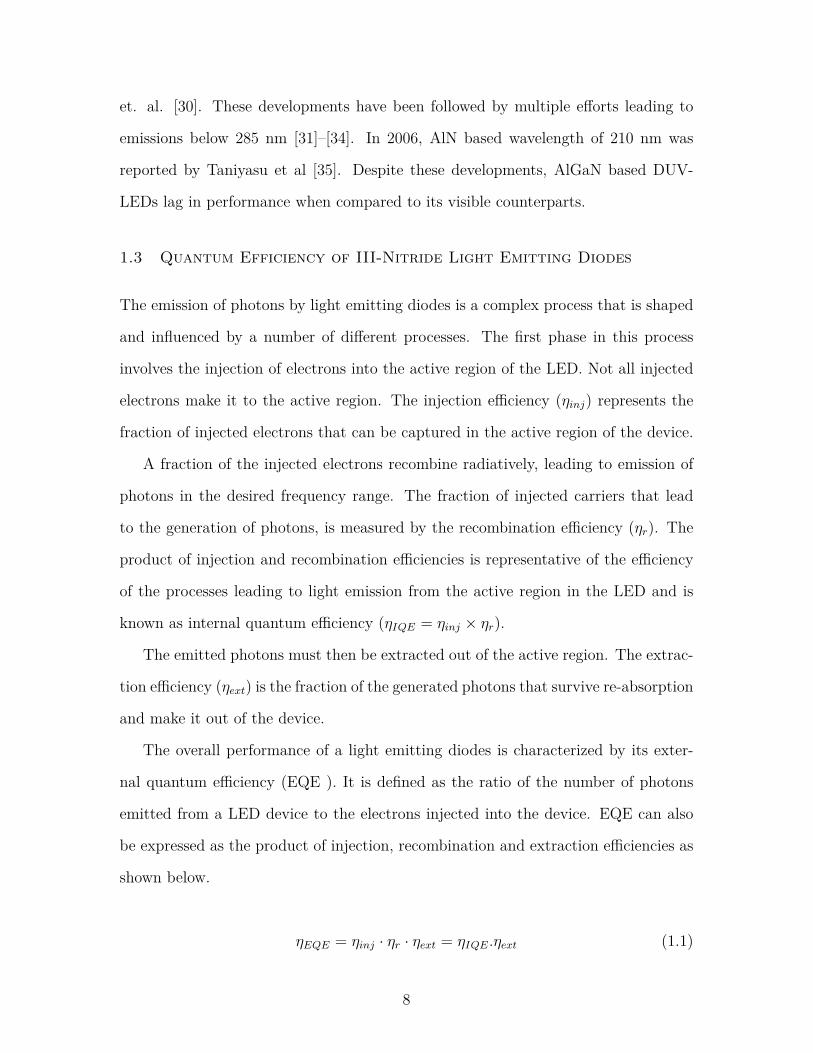
Figure 1.4: Band diagram for GaN/InGaN LED with electron blocking layer [39].
Additionally, the wall-plug efficiency (WPE) can also be used to determine the
performance of a LED. Wall-plug efficiency, also known as power efficiency, is the
optical output power of the device divided by the electrical power supplied to the
LED.
The injected carriers can escape from the quantum wells to the confinement layers,
decreasing the injection efficiency of the device. This loss of carriers can be observed
as an emission peak at longer wavelength other than the desired peak of the LED.
These peaks appear when electrons, instead of being captured in the active region,
pass through it and recombine with holes in the p-type layer [36].
To reduce the carrier leakage out of the active region and to enhance the confine-
ment of electrons in the quantum wells, an electron blocking layer (EBL) is inserted
between the quantum wells and the p-type layer [37]. The electron blocking layer
has a wider band gap and serves as a barrier to these electrons. An EBL is usually
doped p-type, consequently, it offers no barrier to holes. The injection efficiency of
LED device can also be influenced by the thickness of the EBL layer [38]. The band
diagram of InGaN LED with electron blocking layer is shown in Figure 1.4.
The recombination efficiency depends on the ratio of radiative and non-radiative
recombination of carriers. The radiative recombination happens when injected elec-
9

Figure 1.5: Band diagram illustrating non-radiative recombination (a) via de-fects/traps, (b) via auger processes and (c) radiative recombination via band-to-bandrecombination [39].
trons and holes recombine and emit light. The probability of radiative recombination
increases with an increase in concentration of injected carriers. Multiple quantum
wells are generally used to confine these carriers and to increase their concentrations.
Not every recombination leads to emission of photons in the desired frequency
range. Non-radiative recombination occurs when injected carriers get trapped in
the mid-gap defect states, leading to generation of phonons as heat energy. The
number of these defect states in the active region is directly proportional to the
dislocations/defects in the epilayer of the LED device.
Different mechanisms for carrier recombination is depicted in Figure 1.5. Part
(a) in the figure depicts a non-radiative recombination where defects acts as traps
for electrons and holes, causing phonon generation. In part (b), auger processes are
responsible for non-radiative recombination, while part (c) illustrates band-to-band
radiative recombinations, leading to generation of photons (light). Therefore, it is
imperative to grow high quality epilayers in order to improve the radiative recombi-
nation efficiency.
The extraction efficiency can suffer from large differences in the refractive indices
of AlGaN material, sapphire substrate, and air. A difference in refractive indices of
10

Figure 1.6: Diagram illustrating the effect of refractive index mismatch on lightextraction.
adjacent layers determines the critical angle of a surface. According to Snell’s law, if
the emitted light is incident on a surface with an angle larger than the critical angle
for that surface, it is reflected and get absorbed by the material, as shown in the
Figure 1.6. To summarize, the amount of light that can be extracted from the device
can be maximized by curtailing total internal reflection.
A number of different methods have been adopted by various research groups
to increase the light extraction efficiency of LED devices. In [40], for example, the
efficiency of the LED was improved by substrate backside roughening, while surface
texturing of bottom epilayer in thin-film technology was used in [41]–[44]. Patterned
sapphire substrate (PSS) has also been shown to improve the extraction efficiency of
the LED device [45].
The wall plug efficiency is limited by the differential resistance of the LED device.
This differential resistance arises from the cumulative effects of metal contact resis-
tance, the n-AlGaN layer resistance, and the voltage drop across the p-n junction
of LED device. An increase in the voltage drop across the device will increase the
amount of energy needed to push the carriers to the active region, thereby decreas-
11

ing the wall plug efficiency of the device. The resistance of n-AlGaN layer must be
minimized to reduce the operating voltage of a LED. A reduction in resistance can
be achieved by either increasing the doping or increasing the thickness of this layer,
without compromising the crystal quality.
There is tremendous room for improvement in the wall plug efficiency of DUV-
LEDs. For comparison, the wall plug efficiencies for AlGaN-based UV LEDs are
around 1% [46] while the efficiencies for InGaN based red and blue visible LEDs have
reached or exceeded 60% [22].
1.4 Review of III-Nitride Deep Ultraviolet Light Emitting Diodes
The external quantum efficiencies for current state-of-the-art UV LEDs are shown in
Figure 1.7. It is evident from the diagram that InGaN based LEDs, with emission
wavelengths longer than 365 nm, have EQEs of around 14%. However, EQEs remain
low for LEDs based on AlGaN quantum wells; with an EQE of approximately 3% for
LEDs with wavelengths in 280-285 nm range [33], [47], and below 2% for LEDs with
emissions in the UV-C region (200-280 nm). A significant degradation in the EQE
has been reported for devices with shorter wavelengths [48], [49].
There are a number of factors contributing to this low value of EQE for DUV-
LEDs. The high level of defect densities in AlGaN layers lead to a reduced radiative
recombination efficiency. The major contributing factor to the high level of defect
density can be attributed to an unavailability of lattice-matched native substrates.
The AlN substrate, while a high quality substrate, is not readily available nor
is it a cost effective solution. Sapphire is the most suitable substrate commercially,
due to its low cost and sufficient transparency to UV light (down to 150 nm). How-
ever, a downside of using sapphire substrate is the resulting large lattice and thermal
mismatches between sapphire and AlN layers [51]. These lattice and thermal mis-
matches, together with the low surface mobility of Al atoms, can lead to large number
12
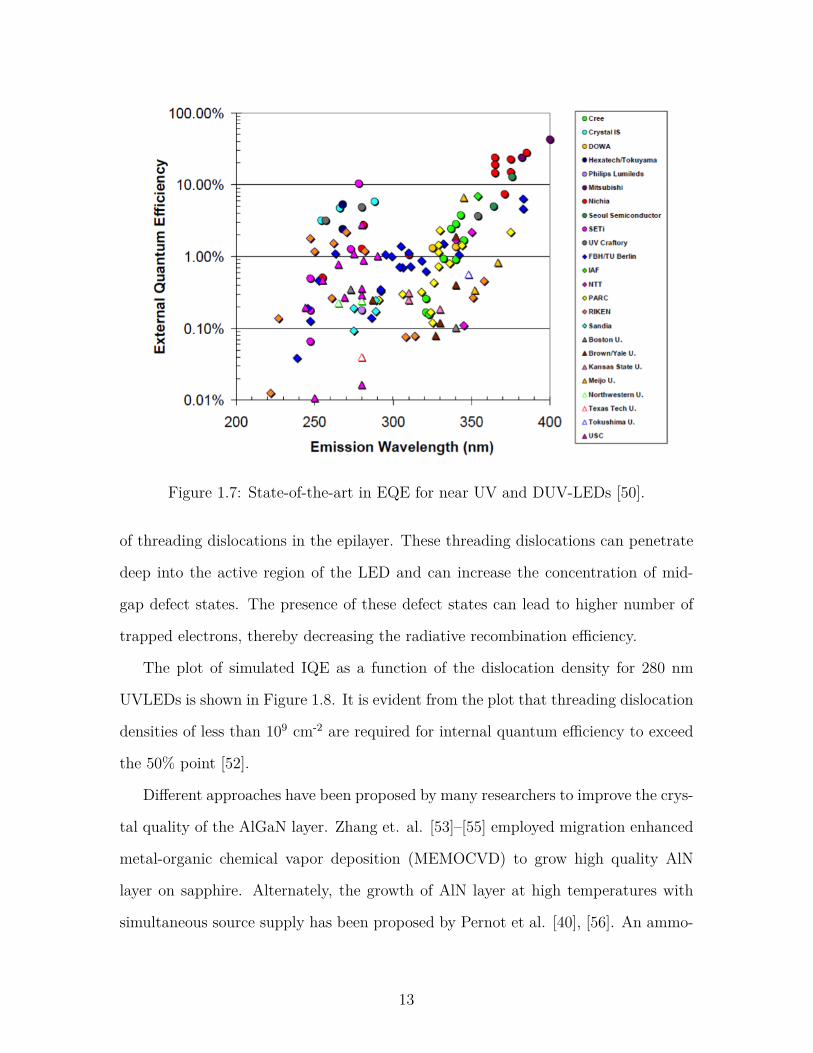
Figure 1.7: State-of-the-art in EQE for near UV and DUV-LEDs [50].
of threading dislocations in the epilayer. These threading dislocations can penetrate
deep into the active region of the LED and can increase the concentration of mid-
gap defect states. The presence of these defect states can lead to higher number of
trapped electrons, thereby decreasing the radiative recombination efficiency.
The plot of simulated IQE as a function of the dislocation density for 280 nm
UVLEDs is shown in Figure 1.8. It is evident from the plot that threading dislocation
densities of less than 109 cm-2 are required for internal quantum efficiency to exceed
the 50% point [52].
Different approaches have been proposed by many researchers to improve the crys-
tal quality of the AlGaN layer. Zhang et. al. [53]–[55] employed migration enhanced
metal-organic chemical vapor deposition (MEMOCVD) to grow high quality AlN
layer on sapphire. Alternately, the growth of AlN layer at high temperatures with
simultaneous source supply has been proposed by Pernot et al. [40], [56]. An ammo-
13

Figure 1.8: Simulated internal quantum efficiency versus the dislocation density for280 nm DUV-LEDs.
nia pulsed-flow multilayer growth has been introduced by Hirayama et al. [49], [57],
[58]. Similarly, AlN layers grown by metal-organic vapor phase epitaxy (MOVPE)
at high temperature, with an optimized nucleation layer, was also demonstrated to
reduce dislocation density [59].
In addition to the growth of high quality AlN buffer layer, AlN/AlGaN or Al-
GaN/AlGaN superlattice (SL) [54], [60] layers have also been used to further fil-
ter the defects and to enable the growth of thick n-AlGaN layer without cracking.
Rough/smooth AlGaN [61] technique has been shown to reduce the defects when
grown before the SL layer. Although these research efforts have brought down the
overall dislocation densities from 1010 cm-2 down to 5x108cm-2 for AlGaN layers, the
internal quantum efficiencies for these devices still remain below 50%.
The doping of AlGaN layers with high Al content is another challenge in DUV-
LEDs. As the aluminum concentration increases, the bandgap of AlGaN layers also
increases, thereby increasing the ionization energy of silicon in the case of n-AlGaN
14
and of magnesium for p-AlGaN layer. The activation energy for Mg dopants in GaN
is already high at 250 meV. This value reaches close to 400 meV with Al content of
70%, resulting in very low conductivity and poor injection of hole carriers.
This low conductivity creates a number of issues in the design of efficient DUV-
LEDs. An increase in the layer resistance results in higher joule heating in the device,
further reducing the device efficiency and reliability. Since it is difficult to make ohmic
contacts directly on p-AlGaN layer, a p-GaN layer is deposited on top of this layer to
serve as a contact layer. This additional layer increases the rate of absorption of the
UV emissions. The p-GaN layer also serves as a potential barrier to the injected holes
before they can be transported across the p-AlGaN layer down to the active region.
The trapped holes at the interface set up an electric field, which attracts the electrons
and allows a fraction of them to bypass the QWs and recombine non-radiatively in
the p-GaN layer, further reducing the injection efficiency. A multi-quantum barrier
electron-blocking layer was employed in [49] to improve the injection efficiency. The
barrier for hole injection can be reduced by grading the composition of p-AlGaN layer
[62].
A number of research efforts have tried to address the issues of light absorption
in the p-GaN contact layer and total internal reflection due to high refractive indices.
The refractive index for AlGaN layers is relatively high with values between 2-2.5.
Consequently, more than 92% of the produced photons are reflected back into the
semiconductor. An encapsulation epoxy with high refractive index can be introduced
to improve light extraction. A disadvantage of this approach is that majority of
encapsulation polymers deteriorate when exposed to UV light for long durations.
Laser lift-off, together with epilayer texturing/roughening, have been employed
in a number of configurations to improve light extraction. Notable variants of this
technique include vertical injection thin-film UVLEDs [63], [64] and lateral injection
thin-film flip-chip UVLEDs [65]–[67]. Other important techniques include moth-eye
15
structures [40], [56], and nano-pixel contact design with Al reflector [68].
The highest reported EQE of 10.4%, at a wavelength of 278 nm, is achieved by a
combination of these techniques [69]. In the first step, the internal quantum efficiency
was maximized by a reduction in dislocation density. Maximum light extraction
was then ensured by using a combination of UV-transparent p-type contact layers,
and UV reflecting ohmic contacts. The transparent p-type contact layer minimizes
light absorption and allow the photons to reach the ohmic contacts which was made
reflective to collect these photons and reflect them back into the device. Finally, an
encapsulation of the device with an epoxy layer, with optimized shape and refractive
index, allowed for maximum extraction of light from the device.
16
Chapter 2
Problem Identification and Characterization
Techniques
2.1 Problem Identification
Sapphire is the substrate of choice for deep ultraviolet light emitting diodes (UV-
LEDs). Sapphire is primarily used due to its low cost, high availability, and optical
transparency to UV radiations down to 150 nm range.
The large lattice and thermal mismatches between sapphire and high Al-content
AlGaN epilayers, however, lead to the formation of a large number of threading
dislocations and cracks in the LED structure. Upon reaching the active region of
the LED, these defects act as non-radiative recombination centers for the injected
carriers, hence reducing the device output power.
In addition to reduced efficiency, the non-radiative recombination process is di-
rectly related to lifetime degradation of LEDs [70]. The energy emitted through the
non-radiative recombination of carriers is usually in the form of phonon (heat), which
dissipates into crystal lattice and accelerate the degradation of the device.
Due to poor doping efficiency of high Al-content n-AlGaN layer, DUV-LEDs ex-
hibit high series resistance, which subsequently leads to higher operating voltage, and
results in low wall-plug efficiency.
The focus of this research is to improve the design of DUV-LEDs, leading to
more efficient growth and fabrication processes, increasing its commercial feasibility
without sacrificing the optical output power or reliability of these devices.
17

Figure 2.1: A typical schematic of DUV-LEDs [73].
In order to reduce dislocations in the active region of the DUV-LEDs grown on
sapphire, an AlN buffer layer is first deposited [53]–[55]. This deposition is followed
by the growth of AlN/AlGaN short-period superlattice, introduced in [54], [60], to
manage strain in the epilayer and filter the dislocations. The introduction of the
superlattice allows for the growth of thick n-AlGaN layer without the formation of
cracks. This fully-relaxed device structure, first developed by [54], has since been
adopted by a number of researchers including [33], [71], [72].
The growth of superlattice is an effective strain management techniques, however,
it suffers from a number of issues. It is a complex and time consuming process that
suffers from the problem of reproducibility, resulting in lower yields and commercial
feasibility. Furthermore, the growth of thick superlattice structures is often plagued
by the introduction of bowing in the resulting wafer which further complicates the
fabrication process. The device schematic for a DUV-LED with superlattice structure
is shown in Figure 2.1.
Another source for reductions in the dislocation density in DUV-LEDs structure is
the use of low defect density bulk AlN substrates instead of sapphire [74]. The defect
density in homoepitaxial AlN buffer layer grown on bulk AlN substrate is more than
2 orders of magnitude lower than the AlN buffer layers grown on sapphire. The
18

bulk AlN based devices generally employ pseudomorphic structures to avoid epilayer
relaxation. The pseudomorphic structures keep the layers strained which otherwise
could lead to increase in defect density from less than 106 cm-2 to over 108 cm-2. The
resulting pseudomorphic AlGaN multi-quantum well structures exhibited dislocation
densities well below 107 cm-2 [75], [76].
The highest reported EQEs for small periphery DUV-LEDs on bulk AlN sub-
strate are very similar to that of DUV-LEDs on sapphire in spite of lower defect
densities. The EQEs were reported to be in the 2.0–3.0% range for LEDs with bulk
AlN substrates [77], [78] while this value is between 3.0–3.5% for those on sapphire
[40], [69].
The lower quantum efficiencies for DUV-LEDs on bulk AlN can be attributed to
a number of factors. The absorption coefficients for AlN substrates is very high in the
deep UV region. Furthermore, these devices generally experience higher stress due
to the substrate thinning process after device fabrication. Moreover, the diameters
of bulk AlN substrates are generally much smaller than sapphire. For comparison,
sapphire substrates are readily available in a wide range of diameters up to 8 inches
while typical values are around 1 inch for bulk AlN. The size limitation for bulk AlN
significantly lowers the yield for high volume device production.
Most importantly, the manufacturing cost for bulk AlN is much higher than sap-
phire. At the time of publication of this dissertation, the market price for a 4-inch
sapphire wafer is approximately $18 while the price for an 1-inch bulk AlN is close
to $5000, making it commercially infeasible for the development of DUV-LEDs.
Consequently, sapphire is the substrate of choice for the development of DUV-
LEDs in high volume production. In this context, a new approach has been developed
by our group to grow high-quality thick (3-5 μm) AlN buffer layers over sapphire
substrates using pulsed metal-organic chemical vapor deposition (MOCVD) [61]. The
devices developed using this approach have threading dislocation densities between
19
(1-5)x108 cm-2.
In this research, these templates have been used to grow the DUV-LEDs employing
the pseudomorphic structure. These pseudomorphic structures, very similar to those
grown on bulk AlN, brings the crystalline quality of active layers closer to that of the
underlying AlN/sapphire template.
In addition to pseudomorphic DUV-LEDs, other designs, based on various degrees
of relaxation of the n-AlGaN layers, have also been investigated in this research. The
primary objective of this research is to achieve an optimal design that attains the
required device characteristics, namely output power and reliability, while simultane-
ously being cost-effective leading to commercial feasibility.
2.2 Material Characterization
In this section, a brief introduction to various material characterization techniques is
presented. These measurements are carried out during the different phases of device
growth and fabrication and can convey vital information regarding the quality of the
fabricated devices.
Sheet Resistance Mapping
The Lehighton contactless sheet resistance mapping system is used in this research
for a fast and nondestructive sheet resistance measurements after the growth of an
LED structure. The sample is placed between two RF coils and eddy currents are
generated by the RF power. The eddy currents are generated primarily in the n-
AlGaN layer owing to its higher conductivity compared to other layers in the LED
structure.
A typical mapping for n-AlGaN sheet resistance can be seen in Figure 2.2. The
sheet resistance has been evaluated at different locations on the wafer surface. The
measurements also provide the average sheet resistance. The standard deviation for
20
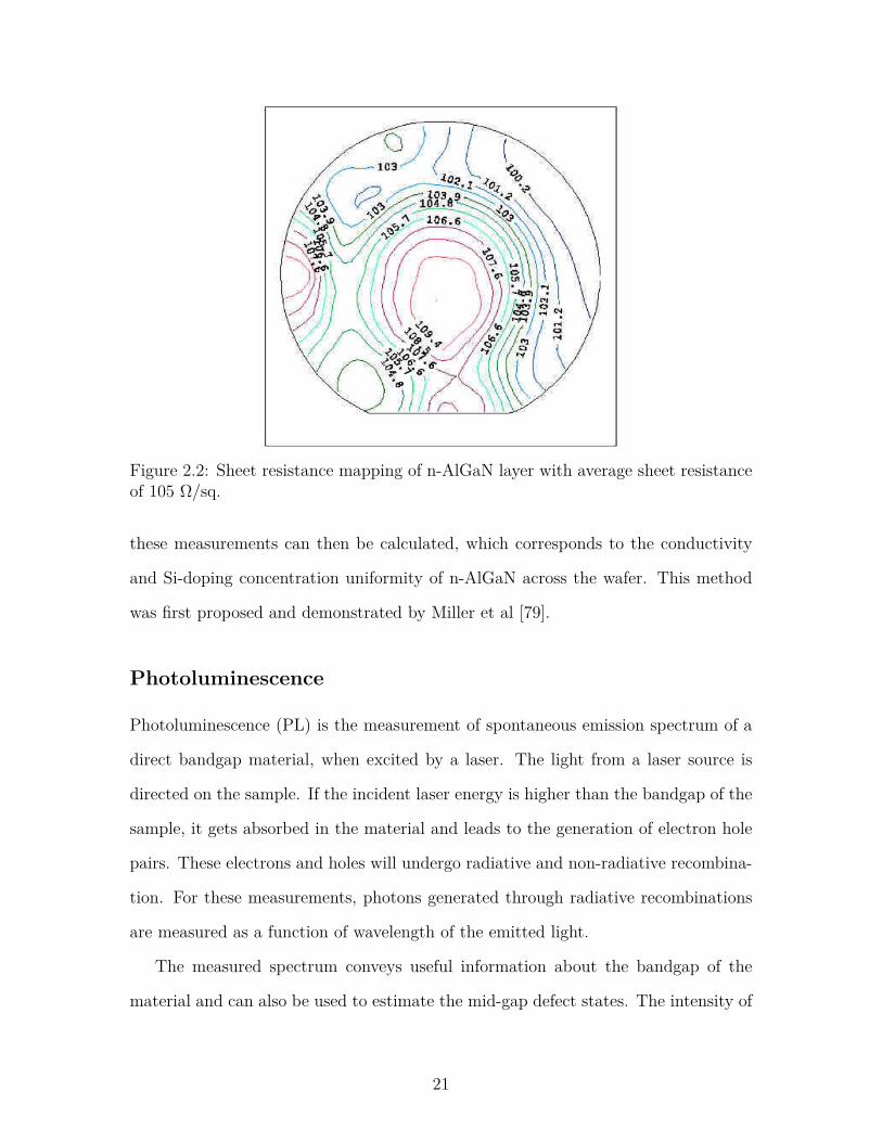
Figure 2.2: Sheet resistance mapping of n-AlGaN layer with average sheet resistanceof 105 Ω/sq.
these measurements can then be calculated, which corresponds to the conductivity
and Si-doping concentration uniformity of n-AlGaN across the wafer. This method
was first proposed and demonstrated by Miller et al [79].
Photoluminescence
Photoluminescence (PL) is the measurement of spontaneous emission spectrum of a
direct bandgap material, when excited by a laser. The light from a laser source is
directed on the sample. If the incident laser energy is higher than the bandgap of the
sample, it gets absorbed in the material and leads to the generation of electron hole
pairs. These electrons and holes will undergo radiative and non-radiative recombina-
tion. For these measurements, photons generated through radiative recombinations
are measured as a function of wavelength of the emitted light.
The measured spectrum conveys useful information about the bandgap of the
material and can also be used to estimate the mid-gap defect states. The intensity of
21

the emitted light and the full width at half maximum (FWHM) values are typically
related to the crystalline quality of the material. A better quality epilayer will have
a higher intensity spectrum and narrower FWHM.
The following equation can be used as a guideline for the selection of laser wave-
length when measuring photoluminescence for a material with a particular direct
bandgap.
Eg = 1249.8/λ. (2.1)
In Equation 2.1, λ denotes the wavelength of a laser in nanometers while Eg
represents the bandgap energy of the material in electron volts. For instance, a 193
nm excimer laser can be used for photoluminescence characteristics measurement of
III-nitrides with bandgap energy up to 6.47 eV.
Atomic Force Microscopy
An atomic force microscope (AFM) generates the surface morphology of an epitaxial
layer with a resolution in the nano-scale range.
For non-destructive measurement, AFM is used in tapping mode (intermittent
contact mode), as shown in Figure 2.3.
During this process, a micro-cantilever with a sharp tip is driven by a piezoelectric
crystal material. The cantilever oscillates (with amplitude of more than 10 nm) up
and down on top of the sample surface with its resonance frequency of about 200
Hz to 400 KHz. The tip experiences a Van der Waals force when it comes in close
proximity to the measured surface. The resulting force decreases the amplitude of
oscillation.
Surface irregularities in the epitaxial layer can be estimated by measuring the
variations in the amplitude of oscillations. When the tip passes a depression in the
surface, the distance between the surface and the cantilever tip increases, which leads
22

Figure 2.3: AFM in tapping mode [80].
to a larger amplitude of oscillation due to lower Van der Waals forces. In contrast,
an increase in this amplitude will be observed when the tip passes over an elevated
point on the surface.
This change in amplitude is measured by a deflecting laser beam attached to a
detector. A feedback system adjusts the height to maintain the oscillation amplitude
of the cantilever as it scans over the sample. The relationship between Van der Waals
forces and inter-atomic spacing is depicted in Figure 2.4 [81]. In tapping mode, an
image is created by imaging the force of intermittent contacts of the cantilever tip
with the surface of the sample [82]. Consequently, any damage to the surface and
tip is decreased as compared to the contact mode of operation. Furthermore, image
resolution is greatly improved due to the elimination of lateral forces between the tip
and the sample.
The AFM image is used to evaluate surface morphologies like surface pits, grain
boundaries and surface atomic steps. The quality of a sample with linear atomic steps
in the AFM image is deemed higher than one with curving, intersecting atomic steps.
The intersection of atomic steps, and the presence of black pits at these intersection
are generally an indication of dislocations. The topographic map of the sample surface
23

Figure 2.4: The Van der Waals forces regime versus distance.
can also be used to derive the root mean square (RMS) of surface roughness.
Etch Pit Density
In this work, etch pit density (EPD) method has been used to acquire the dislocation
density of n-AlGaN layer and AlN/sapphire template. EPD is a fast and simple
technique that is extensively used during growth optimization of each layer of LED
structure. It can be used to obtain the number and type of dislocation densities for
the epitaxial layers based on the defect selective etching process.
In EPD analysis, the sample, cut in 2 cm x 2 cm blocks, is immersed in H3PO4
solution heated at 130◦C for 3-5 minutes. The sample is then removed from the
solution, cleaned thoroughly with de-ionized water, and is blow-dried by nitrogen.
To remove the excess water, the sample is baked in oven for 10-15 minutes.
A high-resolution image is then extracted using atomic force microscopy for defect
analysis and to obtain the dislocation density of the layer. An AFM image of AlN
after etching is shown in Figure 2.5. The AFM image shows clear atomic steps with
a small number of pits at the intersection and termination points of the atomic steps.
24
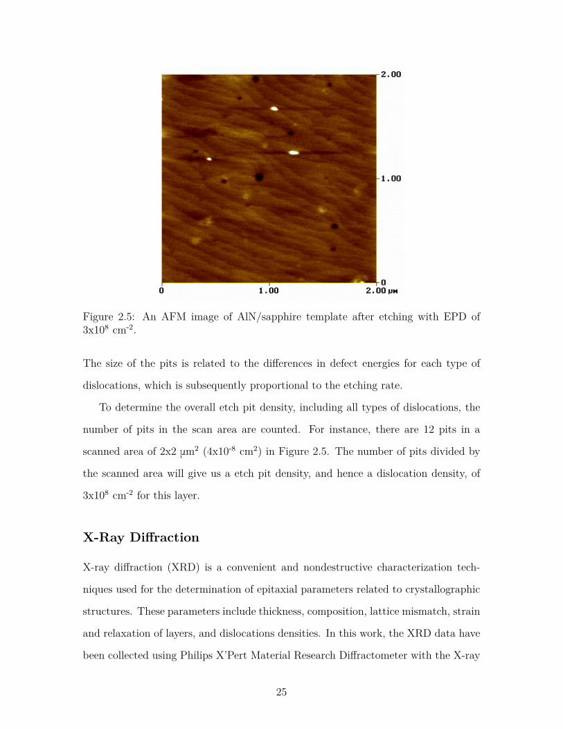
Figure 2.5: An AFM image of AlN/sapphire template after etching with EPD of3x108 cm-2.
The size of the pits is related to the differences in defect energies for each type of
dislocations, which is subsequently proportional to the etching rate.
To determine the overall etch pit density, including all types of dislocations, the
number of pits in the scan area are counted. For instance, there are 12 pits in a
scanned area of 2x2 μm2 (4x10⁻⁸ cm2) in Figure 2.5. The number of pits divided by
the scanned area will give us a etch pit density, and hence a dislocation density, of
3x108 cm-2 for this layer.
X-Ray Diffraction
X-ray diffraction (XRD) is a convenient and nondestructive characterization tech-
niques used for the determination of epitaxial parameters related to crystallographic
structures. These parameters include thickness, composition, lattice mismatch, strain
and relaxation of layers, and dislocations densities. In this work, the XRD data have
been collected using Philips X’Pert Material Research Diffractometer with the X-ray
25

(a) Double Axis Diffractometer (b) Triple Axis Diffractometer
Figure 2.6: Different schemes of X-Ray diffractometers [83].
source wavelength of 1.54 Å.
The diffractometer consists of an X-ray tube, a sample holder, a monochromator,
and an X-ray detector. The X-ray beam is generated in the X-ray tube by the heating
of a filament. The X-rays are passed through a monochromator to get the desired
wavelength. It is then directed to the sample mounted on the sample holder, and the
diffracted beam is collected by a detector.
There are four axes, namely Omega (ω), 2Theta (2θ), Phi (φ) and Psi (ψ) in
a diffractometer. This particular setup is known as a double axis instrument. A
triple axis instrument, with good resolution in the 2θ, can also be made by adding an
analyzer crystal before the detector. This addition, however, will result in an output
with lower intensity. Double and triple axis diffractometers are illustrated in Figure
2.6.
The sample and detector are rotated, and the intensity of the reflected X-rays is
recorded. If the geometry of the incident beam satisfies the condition defined by the
Bragg’s law (2d sin θ = nλ), a constructive interference occurs, appearing as a peak
in intensity. Bragg’s law is illustrated in Figure 2.7.
Mosaicity is created by slight mis-orientations of different crystals as they grow on
the substrate. When the crystals join, they form low energy domain boundaries. To
evaluate the crystal mosaicity of an epilayer, on-axis (002) and off-axis (102) rocking
26

Figure 2.7: Mechanism of X-Ray diffraction.
curves are typically used. The broadening of the rocking curve is translated as the
existence of different orientation grains, thus dislocation density.
The on-axis ω scan gives information about the screw and mixed type dislocations,
which shows the tilt of the lattice planes. The off-axis scan reveals the twists in
the lattice plane, which is an indication of edge type dislocations in a layer. X-ray
diffraction is also used to estimate strain in the epitaxial layers of the LED structure.
This information is crucial since high strain in epilayers can lead to formation of
dislocation and cracks.
The reciprocal space Map (RSM) is a collection of several omega-2Theta coupled
scans. Each coupled scan is collected with a slightly different tilt (offset) in the omega
direction. In this work, RSM is used to characterize the strain in AlGaN layers of
the LED structure.
A reciprocal space map of a fully strained AlGaN MQW structure is shown in
Figure 2.8. The AlGaN peak is positioned on the vertical line drawn from the AlN
peak. This exact alignment of adjacent peaks is an indication of 100% compressive
strain in the layer. The broadening of the reciprocal lattice points indicate imperfec-
tions in the layer crystal, which otherwise should appear as a tiny spot. A detailed
27

Figure 2.8: Reciprocal space mapping showing fully strained AlGaN layer.
discussion of strain in the DUV-LEDs and their manifestation in off-axis reciprocal
space mapping has been discussed in [84].
2.3 Device Characterization
Electroluminescence
The electroluminescence (EL) spectrum is used to measure the peak emission wave-
length of the LED device. In this work, electroluminescence measurements were
carried out using a HORIBA Jobin Yvon Triax 550 spectrometer, equipped with a
600 gr/mm grating and a liquid nitrogen cooled Si CCD detector.
For most applications, a device with emissions concentrated in a small bandwidth
is desired. Such a device must have narrow full width at half maximum (FWHM).
The devices developed in this research have FWHM generally in the range of 10-11
nm. The spectrum is usually plotted on a semi-logarithmic scale, which allows to
discern additional peaks that may be an indication of un-optimized electron blocking
28
layer and quantum wells. Furthermore, it is desirable to have a high (quantum well)
main peak to parasitic peak ratio in a high quality device.
I-V Characteristics
The current-voltage (I-V) characteristics were measured using a Suss MicroTec probe
station and HP parameter analyzer. Like most semiconductor diodes, the I-V charac-
teristic curve is used to analyze the electrical performance of an LED device, such as
turn-on voltage, differential resistance, reverse leakage, series resistance and ideality
factor.
The slope of the linear portion of the I-V curve is equal to the differential resistance
of the device. Moreover, the value at which the linear portion of the I-V curve, when
extended, intercepts the x-axis is defined as the turn-on voltage of the LED. The
turn-on voltage is approximately equal to the bandgap of the material used in the
quantum wells of the LED. The reverse leakage current is typically measured at a
fixed reverse voltage of -1V to -3V for LEDs. At higher values of current, the diode
I-V curve becomes linear due to the dominance of the series resistance. The series
resistance can be measured through an approximation of the I-V curve in the linear
region using the ideal diode equation shown below.
dV
dII = IRs + kT
q(2.2)
The slope of the curve from the dV/dI × I vs. I plot is the series resistance of LED
device.
I-V-L Characteristics
In I-V-L measurements, the light output power is measured as a function of in-
put current, while simultaneously measuring the voltage across the LED. For these
29
measurements, the device is mounted inside an integrating sphere with a calibrated
UV-enhanced Si detector connected to a power meter, while biasing the device using
a HP parameter analyzer.
The measurements can be carried out in two different modes. In the first mode,
known as direct current (dc) or continuous wave (cw) mode, the current is kept at a
constant value. In pulse mode, on the other hand, the current is pumped in, in the
form of pulses. The pulses of current mitigate the self-heating effects, and allow the
device to attain near optimal performance in absence of adverse effects of heating.
The slope of both dc and pulsed mode curves typically overlap at low currents.
Ideally, the output power should increase linearly with an increase in input current.
However, early power saturation (thermal roll-over) sets in as a consequence of heating
effects. Consequently, the slope of the I-V-L curve is generally higher for the pulse
mode measurements at higher values of current due to lower heating.
The I-V-L data can also be used to determine the external quantum efficiency and
wall plug efficiency for an LED device and are generally measured as percentages.
30
Chapter 3
Pseudomorphic Deep Ultraviolet Light
Emitting Diodes over Sapphire 1
1F. Asif, M. Lachab, A. Coleman, I. Ahmad, B. Zhang, V. Adivarahan, and A. Khan, "Deepultraviolet photopumped stimulated emission from partially relaxed AlGaN multiple quantum wellheterostructures grown on sapphire substrates", Journal of Vacuum Science and Technology B, vol.32, no. 6, 0612041, pp. 1-5, 2014.Reprinted here with permission of publisher.
1F. Asif, H. Chen, A. Coleman, I. Ahmad, B. Zhang, J. Dion, A. Heidari, V. Adivarahanand A. Khan, "Pseudomorphic AlxGa1−xN MQW based deep ultraviolet light emitting diodes oversapphire", physica status solidi (c) , vol. 11, no. 3-4, pp. 798-801, 2014.Reprinted here with permission of publisher.
31

Milliwatt power AlGaN-based deep-ultraviolet light emitting diodes over sapphire
substrates were first developed in [85] as part of research efforts to develop a potential
replacement for UV mercury lamps. These devices have potential applications in
air/water purification systems, bio-medical instrumentation and resin curing, among
others.
Since their introduction, several research groups have been working extensively
towards improving and commercializing these devices [33], [40], [58], [77], [86]. The
majority of these studies have employed a relaxed device structure where the active
region comprises of AlGaN multiple quantum wells. These MQWs are generally
deposited over a thick n-AlGaN current spreading layers over short-period superlattice
structure, which was grown on a high quality AlN buffer/c-sapphire templates.
More recently, the use of bulk AlN substrates have been explored to fabricate
DUV-LEDs [77], [78]. The key developments include low-defect density (i.e. <106
cm-2) for the substrates and the observation that for 50-80% Al composition, Si-doped
n-AlGaN material could be grown fully-strained up to a thickness of 1.0 μm [87], and
hence the active layers crystalline quality remains very close to that of the underlying
bulk AlN. These resulted in the demonstration of UV-C LED devices that exhibit up
to 60 mW dc output powers with external quantum efficiency (EQE) between 5 and
6 %.
A similar performance was also reported for LEDs grown on high quality Al-
GaN/sapphire templates [56]. This suggests that photons extraction and low p-type
conductivity represent the other major factors limiting the EQE in nitride-based UV-
C LEDs.
Consequently, sapphire is used as a substrate to fabricate AlGaN MQW based
LEDs in this research. The choice of sapphire, over bulk AlN, is driven primarily due
to cost and availability considerations. However, sapphire offers a number of unique
growth challenges due to its lattice and thermal mismatch with the AlGaN layers.
32
resulting in high number of dislocations density in overlaying layers.
Since these dislocations generated from the heterostructure interface can propa-
gate to the overlaying layers, a smooth and low defect density bottom layer is needed
to reduce the overall defect density in the LED structure, particularly in the active
region of LED. Hence, an thick AlN layer has been successfully used to serve as a
buffer layer between the n-AlGaN layer and the substrate, in order to reduce the
defect density and improve the crystal quality of the subsequent layers.
When growing n-AlGaN layer on AlN buffer layer, the in-plane lattice parameter
of the AlGaN conforms to that of AlN if the thickness of the AlGaN layer is below a
critical value. In this regime, the growth of AlGaN is referred to as pseudomorphic
[88], and all of the strain induced at the hetero-interface is contained within the
AlGaN film, keeping the crystalline quality of the active layer close to that of the
underlying AlN template.
Once the AlGaN is grown beyond its critical thickness, layer cracking and mis-
fit dislocations are introduced due to the strain in the film, leaving numerous non-
radiative centers within the quantum well. These imperfections results in a decline in
the LED internal quantum efficiency and lifetime affecting the device output power
and reliability. This chapter starts with an investigation of the optical quality of the
pseudomorphically-grown MQWs using photo-pumped stimulated emissions. This
introductory discussion is followed by a detailed presentation of growth of full LED
structure, and fabrication of pseudomorphic LED devices. The chapter is concluded
with a detailed presentation of experiments and analysis of observations to evaluate
the performance of pseudomorphic as compared with standard SPSL LED devices.
3.1 Investigation of Epilayer Quality Using Optical-Pumping
The significant progress achieved in deep-UV light emitting diodes over the last few
years has recently re-ignited interests in low-threshold optically pumped sub-300 nm
33
lasing structures. The optical pumping experiments using pulsed excimer laser have
been employed to analyze the optical quality of epilayers without growing and fabri-
cating a complete electrically pumped laser diodes.
The new research efforts build on the prior demonstration of optically pumped
lasing at 214 nm from high quality AlN layers grown by low-pressure metal-organic
chemical vapor deposition (MOCVD) over sapphire substrates [89]. Nearly all the
subsequent studies, however, primarily involved bulk AlN substrates despite its high
cost [90]–[92].
The epilayers designs generally consist of undoped AlGaN QW structures grown
pseudomorphically to prevent generation of new defects due to strain relaxation. This
is because the threading dislocations density in the active region of Al-rich AlGaN
heterostructures emitting in UV-B and UV-C strongly affect their lasing characteris-
tics, and the lower the buffer AlN structural quality the higher the threshold power
density (Pth) [93]–[95].
The total thickness of the top wave-guiding and/or clad layers are generally kept
thin (< 20 nm) when using ArF excimer laser to avoid excessive absorption of the
pump laser radiation away from the active region [91], [92], which invariably leads
to increased threshold. The other parameter that affects the threshold level is the
optical confinement factor [96], which requires a careful optimization of the epilayers
thicknesses and materials compositions. With improvements of the materials qual-
ity and optimization of the heterostructures design, lasing actions with impressive
threshold power densities as low as 84 kW/cm2 were attained in UV-C [90], [91].
These optically pumped stimulated emission have been investigated previously
using a slightly modified design of the MQW structures based on high-quality 285
nm emission DUV-LEDs [95]. The fully-relaxed structure with superlattice still fea-
tured both the n- and p-type doped clad layers to ensure a closer representation of
electrically pumped laser diodes. The threshold power density for the sample in this
34

report was approximately 970 kW/cm2. The threshold value large disparity with that
of AlN substrate-based structures was shown to be primarily due to optical losses in
the top p-clad.
Experiment Procedure
The optically pumped AlGaN heterostructure is schematically illustrated in Figure
3.1. It was grown on a 2-in. (0001) sapphire substrate by low-pressure MOCVD. It
includes a 2.4 μm-thick high quality AlN buffer layer deposited at approximately 1200
ºC on top of a low-temperature (LT) AlN nucleation layer. Typical line-width for
the HT-AlN (102) off-axis X-ray diffraction rocking curve was 360-400 arcsec. The
corresponding dislocation density was estimated to be in the mid-108 cm-2 using etch
pit density technique.
The AlN buffer was followed by a 0.6 μm thick silicon-doped n-Al0.60Ga0.40N, a
four-period undoped multiple quantum wells with 2.5 nm Al0.44Ga0.56N wells sepa-
rated by 21 nm Al0.60Ga0.40N barriers. The active region was capped with Al0.60Ga0.40N
material grown to a thickness of 19 nm. This cap layer acts not only as cladding layer,
but also as surface passivation layer for carrier confinement. Silane (SiH4) was used
for n-type doping.
The MQW wafer was characterized using Philips high-resolution X’Pert MRD
system to determine the strain in the epilayers and room temperature (RT) edge pho-
toluminescence measurements to study the emissions properties in the high pumping
regime. To carry out the optical pumping experiments, laser bars were cleaved along
the a-facet of sapphire substrate to form m-plane mirrors. No extra process step was
undertaken to improve the quality of the mirrors or the quality value (Q-value) of the
lasing cavity. In addition, no reflective coatings were used for the mirror facets. The
cavity length (CL) of the cleaved bars was between 1.4 and 2.3 mm. A 193 nm ArF
excimer laser with a pulse width of 10 ns and a repetition rate of 5 Hz was used as the
35

Figure 3.1: Schematic representation of the optically pumped AlGaN/AlGaN MQWstructure grown on sapphire substrate.
Figure 3.2: Schematic diagram of the setup used for optical pumping experiments.
excitation source. The samples were excited uniformly using a cylindrical lens. The
emitted light was detected by an optical fiber attached to a Triax 550 spectrometer
equipped with a 300gr/mm grating and a liquid nitrogen-cooled CCD detector. The
optical setup schematic is illustrated in Figure 3.2. The detection system resolution
was 0.5 nm.
36
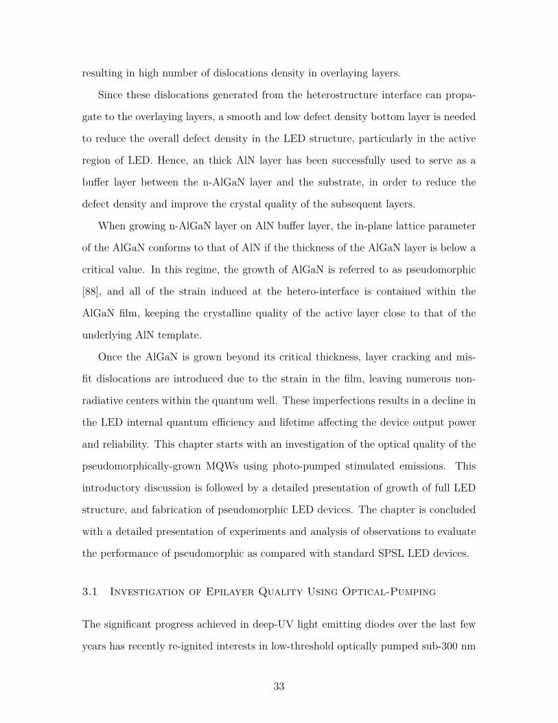
Figure 3.3: Calculated distribution of the optical mode amplitude.
Simulation of Field Distribution and Optical Confinement
Factor Calculation
The optical confinement factor (Γ) of the fundamental transverse electric (TE) mode
of the electromagnetic field for the MQW structure was calculated using a commercial
simulation software. The distribution of the optical mode along the growth direction
can be seen in Figure 3.3.
In the absence of optimized epilayers design, the optical mode was found to leak
outside the active region (formed by the four QWs and three barrier layers) into the
bottom n-AlGaN. Furthermore, the optical field maximum intensity was located away
from the center of the MQWs region. As a result, the optical confinement factor in
the active region was calculated to be about 2.1%. The refractive indices for the
AlGaN compositions of interest were taken from [97].
37
Figure 3.4: RSM of the asymmetric (105) reflection for the photo-pumped AlGaNMQW structure showing a partially relaxed n-AlGaN material with respect to theunderlying AlN buffer layer.
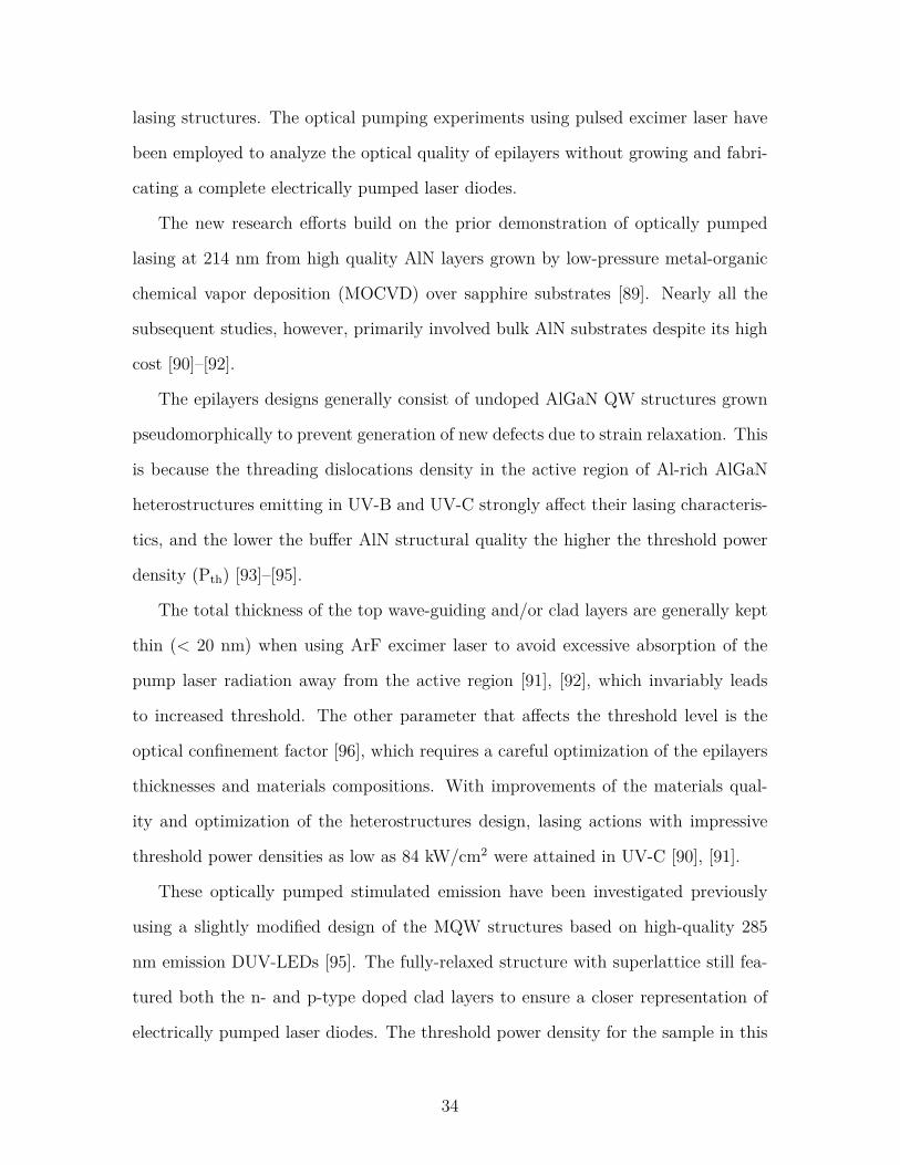
Structural and Optical Characterization of MQW Structures
To analyze the lattice mismatch and stain in the epilayers forming the heterostructure
grown on AlN/sapphire template reciprocal space mapping of the (105) asymmetric
Bragg peak was carried out.
From Figure 3.4, it is evident that the n-AlGaN film reciprocal lattice points
(RLP) do not fall exactly on the vertical line that is perpendicular to the qx axis and
include the RLP of AlN buffer. This indicates that n-AlGaN is not fully-strained
with respect to the underlying AlN material. A partial relaxation of the doped layer,
estimated to be of less than 10%, has thus taken place when grown to the thickness
of 0.6 μm.
In Figure 3.5, the edge photoluminescence spectra for the MQW structure, ac-
quired at room temperature for different laser power densities (PD) between ~53 and
472 kW/cm2, can be seen. The resonator CL was 2.3 mm. At low PD, the PL spec-
tra exhibited a relatively broad spontaneous emission peak at 274.5 nm with 9.7 nm
38

Figure 3.5: Edge PL spectra from the partially relaxed AlGaN/AlGaN MQWs mea-sured at room temperature for different pump power densities.
line-width. As the power density approached 205 kW/cm2, a narrow peak emerged
on the higher wavelength side. The peak then developed into a sharp and strong
emission located at ~276 nm with further increasing PD up to 472 kW/cm2.
The integrated edge PL peak intensity is plotted against the pump power den-
sity in Figure 3.6. A superlinear increase of the emitted light intensity was observed
beyond the threshold, which was estimated to be ~240 kW/cm2. This behavior was
accompanied by a rapid drop in the peak line-width down to 1.2 nm, as illustrated in
Figure 3.6b. Beyond threshold, the peak wavelength exhibited a very small redshift
(≤ 0.5 nm) while the PL emission broadening was limited to less than 0.4 nm. More-
over, the optical output light intensity appeared to saturate when the laser source
was raised above 800 kW/cm2 (i.e. ~3.3 Pth), which is most likely due to materials
39

(a)
(b)
Figure 3.6: Plot of the integrated edge PL intensity (a) and both emission peakwavelength and line-width (b) as a function of the excitation source power densityfor a laser bar with a CL = 2.3 mm. The inset shows optically resolved PL emissionmeasured just around the threshold.
40
degradation in the very high pumping regime.
The stimulated emission properties in laser bars with a smaller cavity were also
measured. The output light-excitation power density at a sample CL of 1.4 mm is
shown in Figure 3.7. As expected, the threshold increased to ~340 kW/cm2. The
simulated emission peak wavelength was in the range 277-278 nm, and similar to the
larger laser bars, both the emission wavelength shift and peak broadening above Pth
remained very small.
The optical properties observed for the partially-relaxed heterostructures clearly
highlight the high quality of the AlN template and the subsequent AlGaN epilay-
ers. For comparison, so far there have been only two reports on optically-pumped
stimulated emission from AlGaN MQW structures on sapphire substrates emitting
in the UV-C region [94], [98]. In one report the threshold for MOCVD-grown MQWs
on epitaxially laterally overgrown (ELO) AlN/c-Al203 templates was greater than
5 MW/cm2 at 272 nm (CL=1-2 mm) [94]. The other work was based on a sin-
gle AlGaN QW grown asymmetrically within a 120 nm thick waveguide over planar
AlN/c-Al2O3 using plasma-assisted molecular beam epitaxy (PAMBE) [98]. Their
cleaved 400 μm long laser cavities exhibited simulated emissions with Pth between
280 and 300 kW/cm2 in the wavelength range 276-278 nm. For both studies the edge
PL was excited by a 266 nm laser source.
To further establish the occurrence of stimulated emission process in our samples
we investigated the polarization properties of the output light for PD=2.3Pth. For
this purpose, aGlan–Thompson polarizer was placed just before the fiber optics at-
tached to the spectrometer entrance port. The results shown in Figure 3.8 indicates
a strongly TE polarized PL emission above threshold. Despite using thicker bottom
n-AlGaN clad and thicker barriers layers, the polarization of stimulated emission is
in good agreement with that previously observed for AlGaN MQW heterostructures
emitting in the range 243-291 nm, which were grown pseudomorphically either on
41
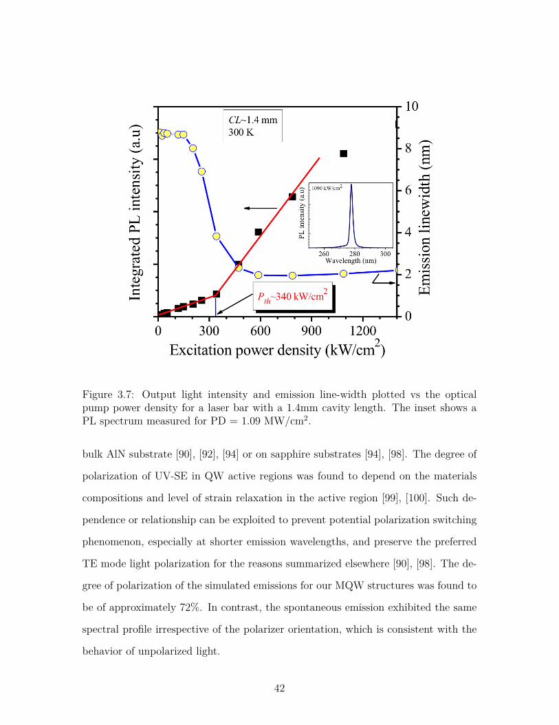
Figure 3.7: Output light intensity and emission line-width plotted vs the opticalpump power density for a laser bar with a 1.4mm cavity length. The inset shows aPL spectrum measured for PD = 1.09 MW/cm2.
bulk AlN substrate [90], [92], [94] or on sapphire substrates [94], [98]. The degree of
polarization of UV-SE in QW active regions was found to depend on the materials
compositions and level of strain relaxation in the active region [99], [100]. Such de-
pendence or relationship can be exploited to prevent potential polarization switching
phenomenon, especially at shorter emission wavelengths, and preserve the preferred
TE mode light polarization for the reasons summarized elsewhere [90], [98]. The de-
gree of polarization of the simulated emissions for our MQW structures was found to
be of approximately 72%. In contrast, the spontaneous emission exhibited the same
spectral profile irrespective of the polarizer orientation, which is consistent with the
behavior of unpolarized light.
42
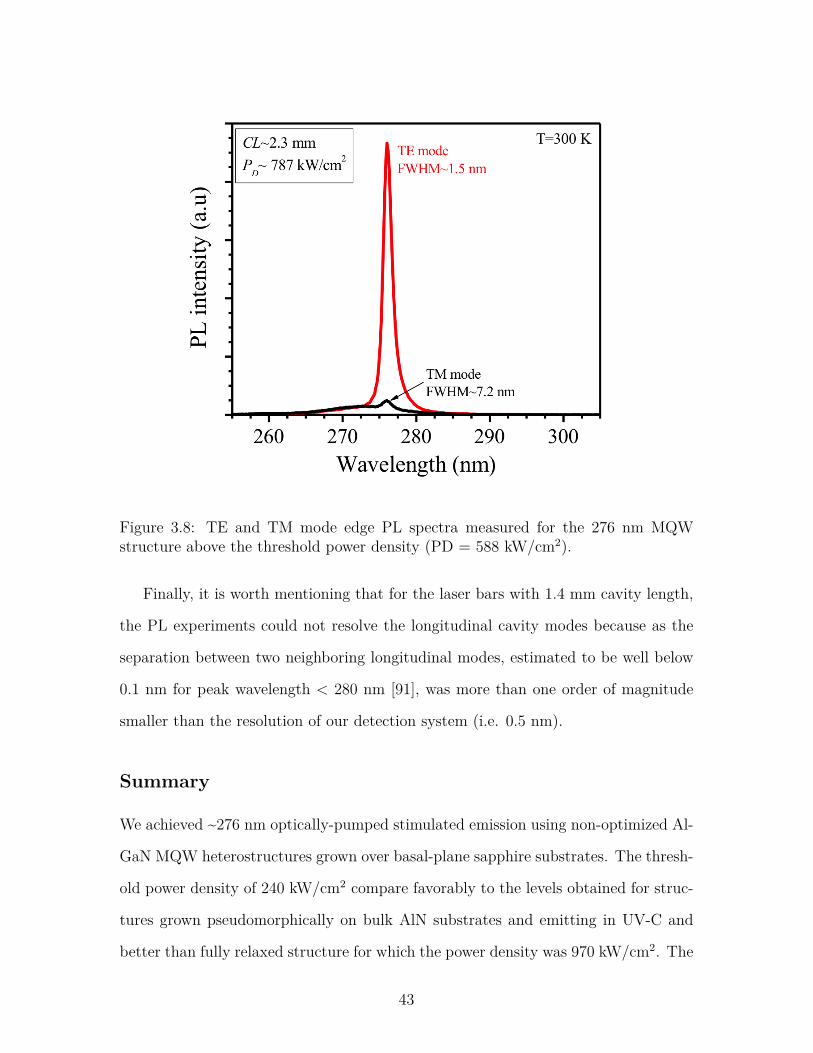
Figure 3.8: TE and TM mode edge PL spectra measured for the 276 nm MQWstructure above the threshold power density (PD = 588 kW/cm2).
Finally, it is worth mentioning that for the laser bars with 1.4 mm cavity length,
the PL experiments could not resolve the longitudinal cavity modes because as the
separation between two neighboring longitudinal modes, estimated to be well below
0.1 nm for peak wavelength < 280 nm [91], was more than one order of magnitude
smaller than the resolution of our detection system (i.e. 0.5 nm).
Summary
We achieved ~276 nm optically-pumped stimulated emission using non-optimized Al-
GaN MQW heterostructures grown over basal-plane sapphire substrates. The thresh-
old power density of 240 kW/cm2 compare favorably to the levels obtained for struc-
tures grown pseudomorphically on bulk AlN substrates and emitting in UV-C and
better than fully relaxed structure for which the power density was 970 kW/cm2. The
43

SE was TE polarized and the minimum emission line-width was 1.2 nm. Moreover,
the emission peak wavelength shift and emission peak broadening were limited to
~0.5 nm above threshold, indicating stable characteristics of the emitted light. These
results suggest that pseudomorphic structures grown over sapphire substrate can pro-
vide a low-cost and reproducible platform for the developments of deep UVLEDs.
3.2 Development of Pseudomorphic Deep Ultraviolet Light Emitting
Diodes
In this section, the fabrication of the first pseudomorphic (PSM) deep UV LEDs on
AlN/sapphire templates, with emissions at 275 nm, is presented. In the pseudomor-
phic growth mode, the thickness of bottom silicon doped n-AlGaN contact layer is
limited to 0.6 μm. This growth constraint results in a relatively low-doping of the
thin n-AlGaN with a high sheet resistance (Rs), which ultimately reduces the LEDs
light output power and reliability. To mitigate these issues, a novel pulsed silicon
modulation doping (PMD) technique [101] has been proposed, in combination with
the micro-pixel design geometry [71] for the growth and fabrication of these devices,
respectively.
LED Structure and Material Characterization
The LED epilayer structure was grown on c-plane sapphire substrate by low-pressure
metalorganic chemical vapor deposition (MOCVD). A 2.4 µm-thick high quality AlN
buffer layer was then deposited at ~1200◦C. Typical linewidth values for the AlN
(102) off-axis X-ray diffraction (XRD) rocking curves ranged from 280 to 330 arcsec.
The FWHM of the (0002) XRD scan for AlN epilayer was measured to be 150 arcsec.
The LED epilayers structure consisted of a 0.6 μm thick, silicon doped Al0.60Ga0.40N,
followed by a five-period Al0.44Ga0.56N/Al0.60Ga0.40N multiple quantum wells, Mg-
doped p-AlGaN electron blocking layers and p-Al0.60Ga0.40N/p-GaN hole injection
44
(a) (b) (c)
Figure 3.9: n-AlGaN sheet resistance for (a) standard SPSL LED, (b) pseudomorphicLED with standard doping and (c) pseudomorphic LED with PMD.
layers. The n-AlGaN layer was deposited using the conventional doping technique,
where the silane (SiH4) gas flow was kept open throughout the process. The layer
sheet resistance was determined to be ~ 900Ω/sq. Next, a novel technique, called
pulsed silicon modulation doping, was used where the SiH4 gas supply was pulsed
using a 50% duty cycle. The material sheet resistance dropped to ~500 Ω/sq, indi-
cating a much better Si atoms incorporation leading to a higher doping level, and
without sacrificing the material structural quality. The sheet resistance of n-contact
layer for standard SPSL LEDs was measured to be 180 Ω/sq, this lower value is due
to higher thickness of n-AlGaN layer. These sheet resistances are depicted in Figure
3.9.
To determine the threading dislocation density in the pseudomorphically grown n-
AlGaN layers, the etch pit density analysis of the epiwafers, grown using conventional
and pulsed n-type doping techniques, was carried out. Both samples were immersed
in phosphoric acid solution heated at 130◦C for 3 min. The samples were then
characterized for the dislocations density using atomic force microscopy. The 2 μm x
2 μm AFM images shown in Figure 3.10 indicate that the PMD approach produced a
better quality material with an EPD of the ~2x108 cm-2 versus ~1.3x109 cm-2 for the
standard n-AlGaN layer, which represents significant improvement in the n-AlGaN
45

(a)
(b)
Figure 3.10: Study of Etch pit Density (EPD) after KOH etching for n-AlGaN withstandard doping (a), and n-AlGaN with PMD doping (b).
46
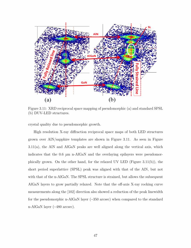
Figure 3.11: XRD reciprocal space mapping of pseudomorphic (a) and standard SPSL(b) DUV-LED structures.
crystal quality due to pseudomorphic growth.
High resolution X-ray diffraction reciprocal space maps of both LED structures
grown over AlN/sapphire templates are shown in Figure 3.11. As seen in Figure
3.11(a), the AlN and AlGaN peaks are well aligned along the vertical axis, which
indicates that the 0.6 μm n-AlGaN and the overlaying epilayers were pseudomor-
phically grown. On the other hand, for the relaxed UV LED (Figure 3.11(b)), the
short period superlattice (SPSL) peak was aligned with that of the AlN, but not
with that of the n-AlGaN. The SPSL structure is strained, but allows the subsequent
AlGaN layers to grow partially relaxed. Note that the off-axis X-ray rocking curve
measurements along the [102] direction also showed a reduction of the peak linewidth
for the pseudomorphic n-AlGaN layer (~350 arcsec) when compared to the standard
n-AlGaN layer (~480 arcsec).
47

(a) (b)
Figure 3.12: Schematics of the DUV-LED epilayer structures: standard SPSL (re-laxed) LED (left) and pseudomorphic LED (right).
Device Fabrication
The fabrication of the LED devices can be explained with the schematic diagram of a
single pixel shown in Figure 3.12. Large area pixel array mesas were first defined using
standard photolithography and reactive ion etching in chlorine plasma. Ti/Al/Ti/Au
and Ni/Au metal stacks were used for the formation of n- and p-contacts, respectively.
The n-contact was annealed at 950 ºC for 30 sec in nitrogen ambient while p contact
was annealed in ambient air at 550 ºC. The pixel LEDs were then isolated using
a planar layer of benzocyclobutene (BCB) followed by shorting of all the pixel p-
contact areas in each device [102]. Each pixel size was 60 μm, which translates into
a total p-active area of 360 x 360 μm2. For comparison, a standard LED epiwafer
grown using a thicker n-AlGaN layer (~2 μm) on top of AlGaN/AlN short-period
superlattice structure was also investigated.
48

Figure 3.13: EL spectrum of pseudomorphic LED measured in dc mode.
Device Electrical and Optical Characterization
Electrical and optical characterization of flip-chip package LEDs were next performed
in dc mode. Electroluminescence (EL) measurements were then carried out using a
HORIBA Jobin Yvon spectrometer, Triax 550, which is equipped with a 600 gr/mm
grating and a liquid nitrogen cooled Si CCD detector. The electroluminescence spec-
trum of the pseudomorphic LED can be seen in Figure 3.13 where the peak emission
is at 275 nm with full width at half maximum of 10 nm. The EL intensity ratio
between the main and the parasitic peaks was around 1000, which is an indication of
good carrier confinement in the MQW active regions [103].
Typical RT current-voltage characteristics of the pseudomorphic and standard
SPSL relaxed devices are illustrated in Figure 3.14 and were measured using a high-
49

Figure 3.14: I-V characteristics of pseudomorphic and standard SPSL LEDs measuredin dc mode. The inset represents SEM image of the pixel-LED device with 360 x 360μm2 p-active area.
resolution digital curve tracer, model Sony/Tektronix 370A. The corresponding diode
series resistances were 23 Ω and 11 Ω, respectively. The high resistance of pseudo-
morphic LED is due to the thin n-AlGaN layer. the inset of Figure 3.14 depicts the
SEM image of the pixel-LED device with 360 x 360 μm2p-active area.
The devices RT output powers were then measured as a function of pump current.
The measurements were carried out using a calibrated integrating sphere. The data
is plotted in Figure 3.15. An output powers of ~7mW and 12mW were measured at
100 mA for the pseudomorphic and standard SPSL LEDs, respectively. The forward
voltages were 8.8 V and 6.2 V, respectively. As a result the PSM LED device exhibits
a lower power saturation current of ~125 mA.
50

Figure 3.15: L-I characteristics measured in dc mode for pseudomorphic and standardSPSL LEDs with 360 x 360 μm2 emission areas.
Reliability of Pseudomorphic DUV-LEDs
For reliability tests, an International Light integrating sphere with a calibrated silicon
photodetector was used to measure the devices output powers, as a function of time
under constant current conditions. Here, 100 x 100 μm2 and 200 x 200 μm2 square-
shaped LED devices were stressed at 20mA dc injection current, which translates into
current densities of 200 A/cm2 and 50 A/cm2, respectively. The lifetime data plots
for several devices with different packaging schemes can be seen in Figure 3.16.
The results indicate an initial steep drop (of more than 30%) in the output power
of the pseudomorphic devices due to self-heating effects resulting from the thin n-
AlGaN layer, and the associated increase of the junction temperature [104]–[106]. The
initial power drop thus becomes important with increasing the pump current density,
51

Figure 3.16: lifetime testing data for packaged pseudomorphic LEDs at RT withdifferent packaging schemes. For comparison, reliability of a reference standard SPSLLED was also measured.
while keeping the other packaging parameters the same, and decreases with improving
heat dissipation through efficient packaging schemes. For example, when the device is
mounted on a TO-3 header and a higher thermal conductivity die attach epoxy (curve
in red color), the output power drop was only 15%. The standard SPSL LED, also
mounted on a TO-3 header, shows only 8% drop as the sheet resistance of n-AlGaN
for standard SPSL LEDs is three times lower than that of pseudomorphic LEDs.
The output power initial rapid decay is followed by a much slower decay over time.
This slower degradation is believed to be due to gradual activation of dislocations in
the active region of the device [107], [108]. These dislocations get activated under
constant stress, leading to non-radiative recombination and hence decay of output
power. However, in the case of pseudomorphic LEDs, the power appears to stabilize
52
(reach a constant level) after about 30 hours of stress, due to better materials quality,
hence exhibiting better device reliability than standard SPSL LEDs.
Summary
In conclusion, the first pseudomorphic deep-UV LEDs has been grown on AlN/sapphire
templates by incorporating a number of innovations in the growth process. A novel
pulse modulation doping technique has been used to improve doping in the 0.6 μm
thick n-AlGaN layer. LED devices with 360 x 360 μm2 p-contact areas were then
fabricated using pixel-LED design geometry. Output powers of ~7 mW at 100 mA
current injection were measured together with a forward voltage of ~ 8.8 V.
The significant improvement in the device reliability of the pseudomorphic LED
devices looks very promising. Although the reference (relaxed) LEDs output power
was better than that of the pseudomorphic devices, more recent results reveal that
there is still room for improvements in LED performance using a quasi-pseudomorphic
growth approach, for which the results will be presented in Chapter 4.
53

Chapter 4
Quasi-Pseudomorphic Deep Ultraviolet Light
Emitting Diodes over Sapphire
The thin n-AlGaN layer in pseudomorphic growth introduces a serious concern in the
form of high sheet resistance due to its reduced thickness. This high sheet resistance
proved to be a deterrent to device output power and reliability as was discussed in
Chapter 3.
It is imperative to address the heating issues by growing thicker n-AlGaN while
maintaining low dislocation density. This goal must be achieved by keeping the
epilayers mostly strained, so that the dislocations density remain close to that of the
starting template. The thicker n-AlGaN layer exhibits better sheet resistance, which
alleviates the current crowding and device self heating issues, thereby, increasing the
device output power and lifetime.
The main advantage of this approach over comparable strain management tech-
niques comes from the straightforward growth process. For comparison, short-period
superlattice structures, an alternate strain management scheme, require complex and
time consuming steps that can lead to increased fabrication cost and lower commer-
cial feasibility. Furthermore, thick superlattice structures also suffer from issues such
as severe substrate bowing, further reducing the yield of these structures.
A novel quasi-pseudomorphic LED structure is introduced in this chapter that
offers low sheet resistance, low dislocation densities, and a straightforward growth
and fabrication process. In the following sections, the growth and fabrication pro-
54
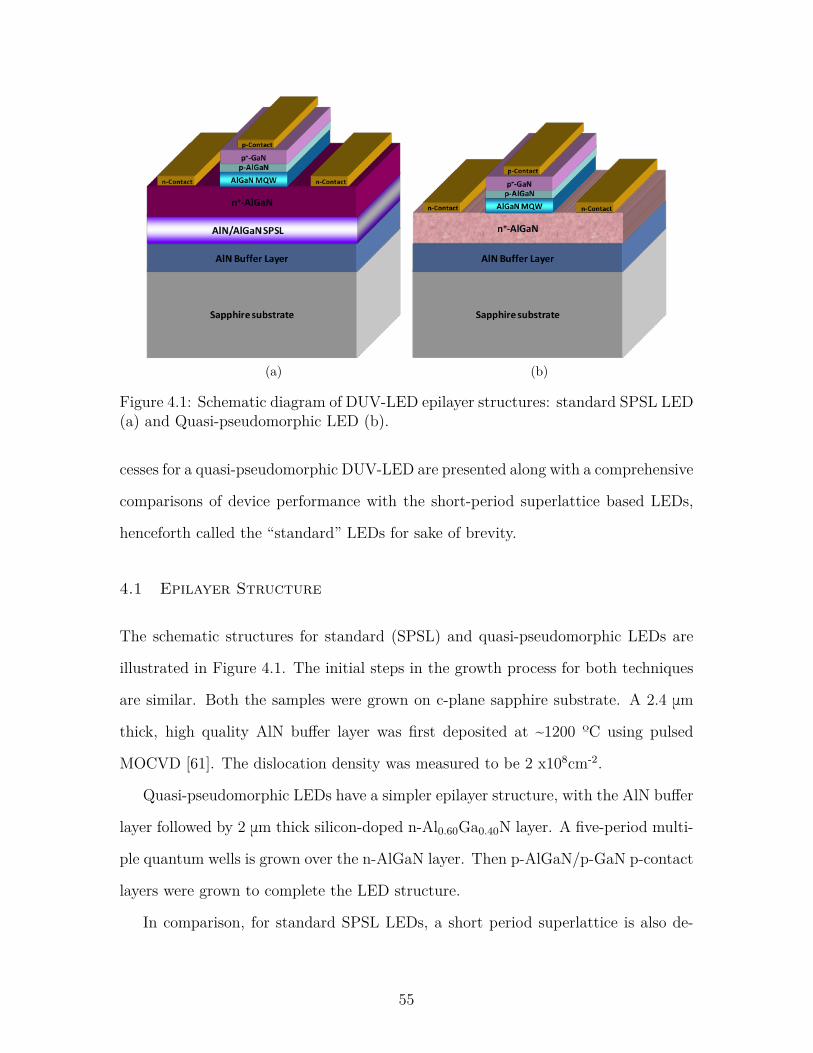
(a) (b)
Figure 4.1: Schematic diagram of DUV-LED epilayer structures: standard SPSL LED(a) and Quasi-pseudomorphic LED (b).
cesses for a quasi-pseudomorphic DUV-LED are presented along with a comprehensive
comparisons of device performance with the short-period superlattice based LEDs,
henceforth called the “standard” LEDs for sake of brevity.
4.1 Epilayer Structure
The schematic structures for standard (SPSL) and quasi-pseudomorphic LEDs are
illustrated in Figure 4.1. The initial steps in the growth process for both techniques
are similar. Both the samples were grown on c-plane sapphire substrate. A 2.4 μm
thick, high quality AlN buffer layer was first deposited at ~1200 ºC using pulsed
MOCVD [61]. The dislocation density was measured to be 2 x108cm-2.
Quasi-pseudomorphic LEDs have a simpler epilayer structure, with the AlN buffer
layer followed by 2 μm thick silicon-doped n-Al0.60Ga0.40N layer. A five-period multi-
ple quantum wells is grown over the n-AlGaN layer. Then p-AlGaN/p-GaN p-contact
layers were grown to complete the LED structure.
In comparison, for standard SPSL LEDs, a short period superlattice is also de-
55

posited before the growth of 3 μm silicon doped n-AlGaN layer.
4.2 Material Characterization
After the growth of the two samples, a detailed analysis of the characteristics of the
two epiwafers was carried out.
Etch Pit Density
The n-AlGaN dislocation density of 5 x108 cm-2and 2 x109 cm-2were measured for
quasi-pseudomorphic and standard SPSL LEDs respectively. Due to quasi growth,
the dislocation density of n-AlGaN remain very close to the template, translating
into four times lower dislocation density as compared to the standard LEDs with
superlattice structure.
Sheet Resistances
The measured sheet resistances for these LED samples are shown in Figure 4.2. The
sheet resistance for quasi-pseudomorphic LEDs decreases with increasing thickness
of n-AlGaN layer. The average value for sheet resistance was 159 Ω/sq as compared
to the 500 Ω/sq for the pseudomorphic LED wafer with 0.6 μm n-AlGaN layer. As
expected the sheet resistance for standard SPSL LEDs was found to be 105 Ω/sq,
owning to a thicker n-AlGaN layer.
XRD Reciprocal Space Mapping
Comparisons of the X-ray diffraction reciprocal space maps of quasi-pseudomorphic
and standard SPSL DUV-LED structures are shown in Figure 4.3. As seen the AlN
and n-AlGaN films reciprocal lattice points (RLP) are not exactly on the vertical
line that is perpendicular to the qx axis, indicating a partial relaxation of the n-
56

(a) (b)
Figure 4.2: Sheet resistance mapping of Standard SPSL LED (a) and Quasi-pseudomorphic LED (b).
AlGaN with respect to the underlying AlN layer, when grown to a thickness of 2
μm. However, it remains mostly strained as compared to the fully relaxed n-AlGaN
for standard SPSL LEDs (see Figure 4.3b), indicating a better crystal quality for
quasi-pseudomorphic LEDs, as the layer relaxation creates defects in LED epilayer.
Summary
The primary advantage of quasi-pseudomorphic epilayers are rooted into a simpler
growth and fabrication process that can lead to significant reductions in manufactur-
ing time and cost. The comparisons in the last sections reveal that despite having sim-
pler growth and fabrication processes, quasi-pseudomorphic LEDs have higher quality
crystals that exhibit lower dislocation densities than those with SPSL structures. The
sheet resistances have improved significantly over pseudomorphic LED but still trail
behind standard SPSL LEDs. However, the thickness of quasi-pseudomorphic n-
AlGaN can be increased further to further reduce the sheet resistance, albeit at the
cost of higher density of defects.
57
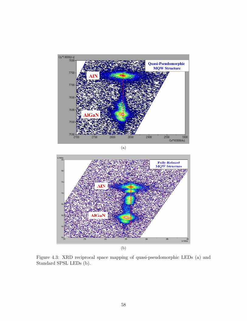
(a)
(b)
Figure 4.3: XRD reciprocal space mapping of quasi-pseudomorphic LEDs (a) andStandard SPSL LEDs (b).
58

4.3 Device Processing
After growth and material characterization, both the samples were processed and
packaged before the final evaluation of their electrical and optical characteristics.
H-shaped mesas were defined to reach the bottom n-AlGaN layer by inductively
coupled plasma reactive ion etching. Once these mesas were formed, n and p ohmic
contacts were laid out by using electron beam evaporation technique. Ti/Al/Ti/Au
and Ni/Au metal stacks were used for n and p ohmic contacts respectively. A probe
contact containing Ti/Ni/Au was also deposited on n and p contacts to make the
contacts thicker for probing purposes. Finally, electroplated Au layer was deposited
on top of n and p contacts before the individual devices were diced.
UV light is collected from the sapphire side of the device, hence, the individ-
ual diced chips (devices) were flip-chip bonded to ceramic AlN submounts using Au
bumps. The flip-chip devices were then mounted on TO-3 headers for device charac-
terization.
The device total p-active area was equal to 200 × 200 μm2 . The processing and
packaging parameters of both devices, including the device active area, were kept
constant for the sake of comparison.
4.4 Electrical and Optical Characterization of Devices
In the following sections, the measured electrical and optical characteristics of quasi-
PSM and standard SPSL LEDs are presented and compared in detail.
Device Electroluminescence
The electroluminescence spectrum for quasi-pseudomorphic and standard SPSL LED
devices are plotted in Figure 4.4. These measurements were carried out using Horiba
59

Figure 4.4: RT normalized EL spectra of Quasi-pseudomorphic and standard SPSLDUV-LEDs measured at 20mA pump current.
Jobin Yvon spectrometer, Triax 550, equipped with a 600 gr/mm grating and a liquid
nitrogen cooled Si CCD detector.
It can be seen in Figure 4.4 that the dominant main peak for both devices occurred
at approximately 270 nm. The value of full width at half maximum was 10 nm for
both quasi-pseudomorphic and standard SPSL devices.
A long wavelength side peak centered at 410 nm can also be seen in both the EL
spectra. This secondary peak is a result of an overflow of the injected electrons to
the deep level of the p-GaN. This leakage can be mitigated by further optimization
of the electron blocking layer. The rate of leakage can be controlled by changing the
thickness and/or composition of the blocking layer. However, the ratio of main to
parasitic emission peaks is measured to be greater than 1500, indicating very good
carrier confinement in the active region [103]. The existence of a short wavelength
emission shoulder centered at ~ 257 nm can be attributed to carrier recombinations
60
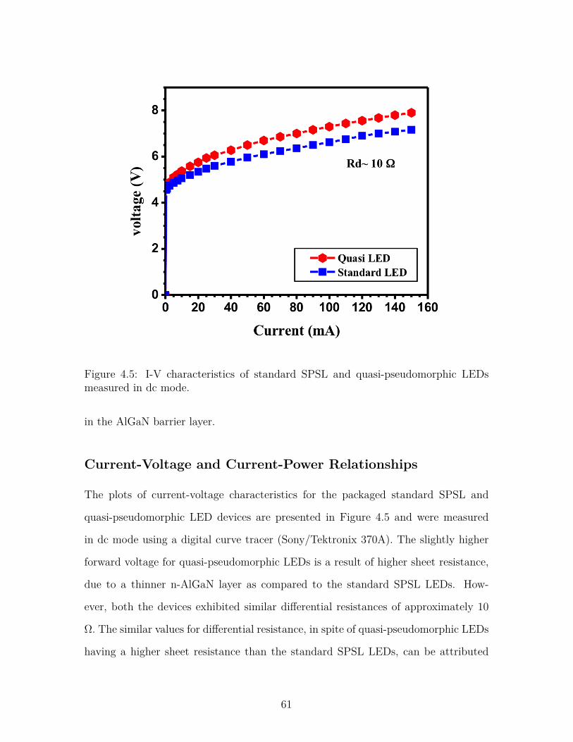
Figure 4.5: I-V characteristics of standard SPSL and quasi-pseudomorphic LEDsmeasured in dc mode.
in the AlGaN barrier layer.
Current-Voltage and Current-Power Relationships
The plots of current-voltage characteristics for the packaged standard SPSL and
quasi-pseudomorphic LED devices are presented in Figure 4.5 and were measured
in dc mode using a digital curve tracer (Sony/Tektronix 370A). The slightly higher
forward voltage for quasi-pseudomorphic LEDs is a result of higher sheet resistance,
due to a thinner n-AlGaN layer as compared to the standard SPSL LEDs. How-
ever, both the devices exhibited similar differential resistances of approximately 10
Ω. The similar values for differential resistance, in spite of quasi-pseudomorphic LEDs
having a higher sheet resistance than the standard SPSL LEDs, can be attributed
61

Figure 4.6: The plot of dc output power as a function of pump current for standardSPSL and quasi-pseudomorphic packaged LEDs measured at RT.
to higher carrier mobility in quasi-pseudomorphic epilayers, and is an indication of
better crystal quality.
A comparison of output power versus injection current plots, measured at room
temperature, for quasi-pseudomorphic and standard SPSL packaged LEDs can be
seen in Figure 4.6. An integrating sphere with a calibrated UV-enhanced Si detector
was used for these measurements.
The output power of the quasi-pseudomorphic LED was expected to be lower, at
the same value of injection current, due to a higher operating voltage. The output
powers at lower injection currents are very similar for both devices, with an output
power of approximately 1 mW measured at a current of 20 mA. In this region, self-
heating is not a serious issue and the quasi-pseudomorphic LED achieved comparable
62
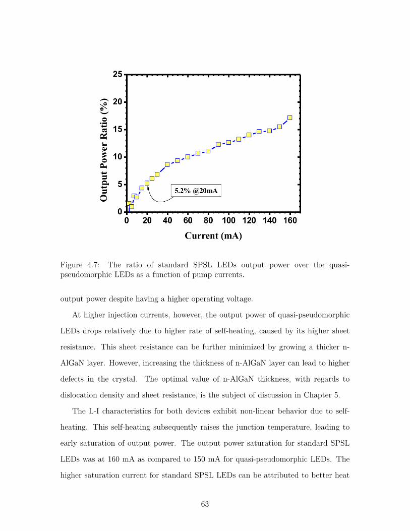
Figure 4.7: The ratio of standard SPSL LEDs output power over the quasi-pseudomorphic LEDs as a function of pump currents.
output power despite having a higher operating voltage.
At higher injection currents, however, the output power of quasi-pseudomorphic
LEDs drops relatively due to higher rate of self-heating, caused by its higher sheet
resistance. This sheet resistance can be further minimized by growing a thicker n-
AlGaN layer. However, increasing the thickness of n-AlGaN layer can lead to higher
defects in the crystal. The optimal value of n-AlGaN thickness, with regards to
dislocation density and sheet resistance, is the subject of discussion in Chapter 5.
The L-I characteristics for both devices exhibit non-linear behavior due to self-
heating. This self-heating subsequently raises the junction temperature, leading to
early saturation of output power. The output power saturation for standard SPSL
LEDs was at 160 mA as compared to 150 mA for quasi-pseudomorphic LEDs. The
higher saturation current for standard SPSL LEDs can be attributed to better heat
63
dissipation due to thicker device structure. As discussed earlier, the saturation point
for quasi-pseudomorphic LEDs can be improved by growing a thicker n-AlGaN layer.
The ratio of standard SPSL LEDs output power over the quasi-pseudomorphic
LEDs is plotted in Figure 4.7. It has to be emphasized here that these devices are
small area devices and are generally operated at low injection currents. For a typical
dc input current of 20mA, the output power of standard SPSL LED is only 5.2%
higher than that of a quasi-pseudomorphic LED.
Device External Quantum Efficiency
The external quantum efficiencies as a function of injection currents is plotted in
Figure 4.8. The plots for both the devices exhibit similar characteristics and can
be divided into two regions. In the first region, the EQE increases rapidly with an
increase in the injection current until it reaches a maximum value. The peak values
of 1.1% and 1.2% were observed for quasi-pseudomorphic and standard SPSL LEDs
respectively, indicating very similar performance between both devices.
Once the maximum value of EQE is achieved, any further increase in the input
current leads to higher rate of self heating rather than light emission, reducing the
overall EQE.
Device Reliability Test
For the reliability measurements, the output power under constant dc current was
monitored as a function of time using an integrating sphere with a calibrated Si
photodiode. The measurements were carried out at room temperature. The H-
shaped LED devices, with an area of 200x200 μm2 each, were stressed at dc injection
current of 20 mA, which corresponds to a current density of 50 A/cm2. The plots
for output power decay for quasi-pseudomorphic and standard SPSL DUV-LEDs are
shown in Figure 4.9.
64
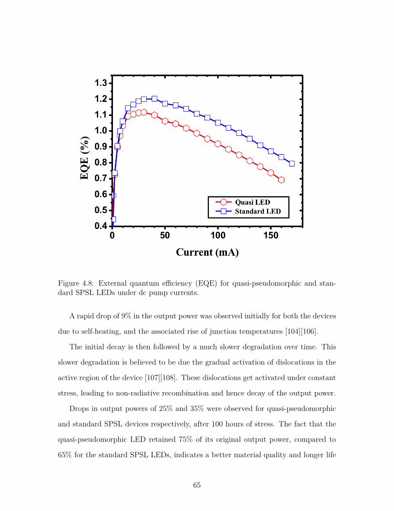
Figure 4.8: External quantum efficiency (EQE) for quasi-pseudomorphic and stan-dard SPSL LEDs under dc pump currents.
A rapid drop of 9% in the output power was observed initially for both the devices
due to self-heating, and the associated rise of junction temperatures [104][106].
The initial decay is then followed by a much slower degradation over time. This
slower degradation is believed to be due the gradual activation of dislocations in the
active region of the device [107][108]. These dislocations get activated under constant
stress, leading to non-radiative recombination and hence decay of the output power.
Drops in output powers of 25% and 35% were observed for quasi-pseudomorphic
and standard SPSL devices respectively, after 100 hours of stress. The fact that the
quasi-pseudomorphic LED retained 75% of its original output power, compared to
65% for the standard SPSL LEDs, indicates a better material quality and longer life
65
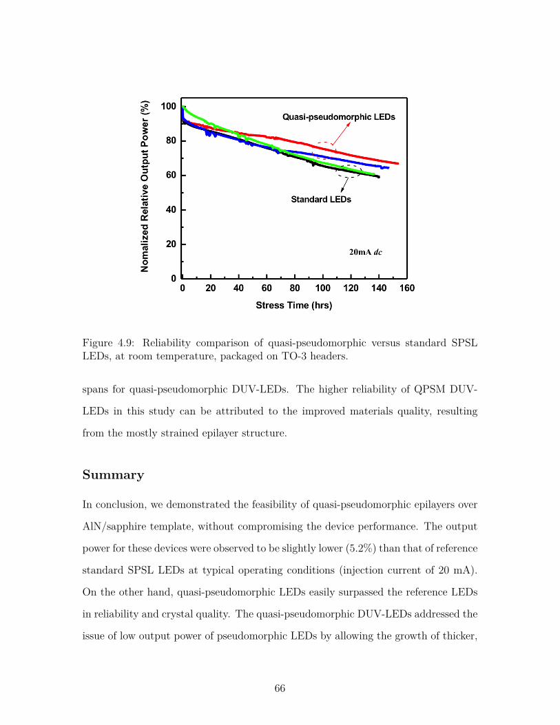
Figure 4.9: Reliability comparison of quasi-pseudomorphic versus standard SPSLLEDs, at room temperature, packaged on TO-3 headers.
spans for quasi-pseudomorphic DUV-LEDs. The higher reliability of QPSM DUV-
LEDs in this study can be attributed to the improved materials quality, resulting
from the mostly strained epilayer structure.
Summary
In conclusion, we demonstrated the feasibility of quasi-pseudomorphic epilayers over
AlN/sapphire template, without compromising the device performance. The output
power for these devices were observed to be slightly lower (5.2%) than that of reference
standard SPSL LEDs at typical operating conditions (injection current of 20 mA).
On the other hand, quasi-pseudomorphic LEDs easily surpassed the reference LEDs
in reliability and crystal quality. The quasi-pseudomorphic DUV-LEDs addressed the
issue of low output power of pseudomorphic LEDs by allowing the growth of thicker,
66
low resistance n-AlGaN layer without sacrificing the crystal quality resulting from a
mostly strained layer. The proposed approach achieved these goals by simplifying the
growth and fabrication processes leading to time and cost savings. Furthermore, by
eliminating the need for short-period superlattices, this approach avoids the severe
substrate bowing issues that plagued the fabrication of standard SPSL devices.
67
Chapter 5
Selective Area Deposition for Deep
Ultraviolet Light Emitting Diodes over
Sapphire
In Chapter 3, we presented the design, fabrication, and characterization of pseudo-
morphic LEDs. In these devices, the MQW structure is fully strained leading to low
levels of dislocation density. As a result, these devices have higher reliability and
longer life spans than fully relaxed SPSL LEDs. However, the output power was
almost 50% less than that of SPSL LEDs owing to the thin AlGaN layer.
The output power limitations led to the development of quasi-pseudomorphic
LEDs, with partially relaxed MQW structure. The quasi-pseudomorphic LEDs offer
output power comparable to standard SPSL LEDs with significantly improved reli-
ability. However, the higher value of sheet resistance, and its contribution to joule’s
heating, is an issue that must be resolved in order to develop efficient, high output
DUV-LEDs.
In this chapter, efforts to grow even thicker n-AlGaN layers have been described.
In Section 5.1, attempts were made to grow epilayers with thickness ranging from 2-4
μm. At these values of thickness, the epilayers are no longer strained. Although the
sheet resistance is reduced by the increased thickness, the defect density increases
significantly due to varying degree of relaxation in the epilayers. The object of these
experiments was to estimate the optimal value of thickness that lead to maximum
value of output power while preserving the quality of the crystals.
68

(a) (b) (c)
Figure 5.1: Schematic diagram of DUV-LEDs with different n-AlGaN thickness.
The results of these experiments led us to the next approach of using selective
area deposition (SAD) for growing thick n-AlGaN epilayers. Selective area deposition
have been successfully used on silicon substrate and Section 5.2 provides the details
of our efforts to adapt this technique for DUV-LEDs over a sapphire substrate.
5.1 The Effects of n-AlGaN Thickness on Device Performance
To study the effects of n-AlGaN thickness on device performance, three LEDs struc-
tures of varying thicknesses were grown on a 5 μm AlN buffer layer, grown on sapphire
substrate. The thickness of the n-AlGaN layers were kept at 2 μm, 3 μm and 4 μm
for device A, B and C respectively. No additional strain relief superlattice layers were
grown for any of these devices. The device schematics are illustrated in Figure 5.1.
Other growth parameters were similar to those described in Chapter 3.
Sheet Resistance
The sheet resistance of n-AlGaN for each sample was measured using Lehighton
contactless sheet resistance mapping system. The sheet resistance mappings for these
LED samples are shown in Figure 5.2. The value of sheet resistances for device A,
69
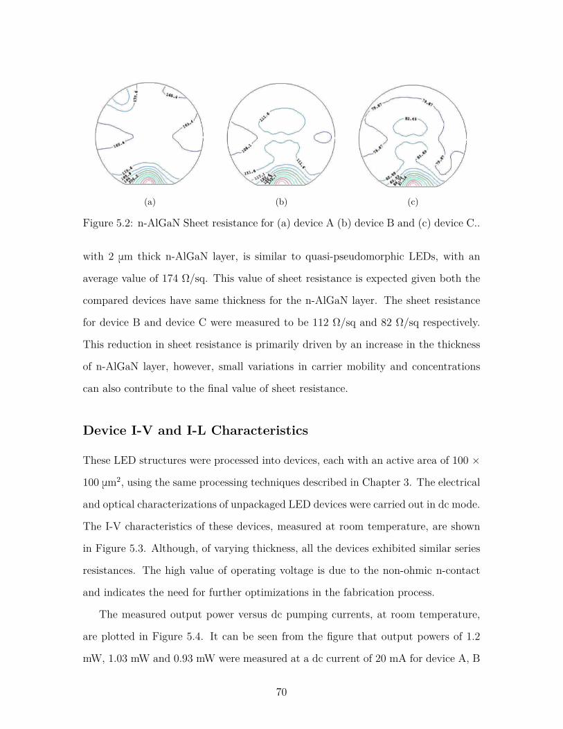
(a) (b) (c)
Figure 5.2: n-AlGaN Sheet resistance for (a) device A (b) device B and (c) device C..
with 2 μm thick n-AlGaN layer, is similar to quasi-pseudomorphic LEDs, with an
average value of 174 Ω/sq. This value of sheet resistance is expected given both the
compared devices have same thickness for the n-AlGaN layer. The sheet resistance
for device B and device C were measured to be 112 Ω/sq and 82 Ω/sq respectively.
This reduction in sheet resistance is primarily driven by an increase in the thickness
of n-AlGaN layer, however, small variations in carrier mobility and concentrations
can also contribute to the final value of sheet resistance.
Device I-V and I-L Characteristics
These LED structures were processed into devices, each with an active area of 100 ×
100 μm2, using the same processing techniques described in Chapter 3. The electrical
and optical characterizations of unpackaged LED devices were carried out in dc mode.
The I-V characteristics of these devices, measured at room temperature, are shown
in Figure 5.3. Although, of varying thickness, all the devices exhibited similar series
resistances. The high value of operating voltage is due to the non-ohmic n-contact
and indicates the need for further optimizations in the fabrication process.
The measured output power versus dc pumping currents, at room temperature,
are plotted in Figure 5.4. It can be seen from the figure that output powers of 1.2
mW, 1.03 mW and 0.93 mW were measured at a dc current of 20 mA for device A, B
70

Figure 5.3: devices I-V characteristics measured at RT.
and C respectively. The result shows a decrease of LEDs output power with increase
in n-AlGaN thickness.
It can be hypothesized that an increase in the n-AlGaN thickness beyond 2 μm,
which was the thickness for our quasi-pseudomorphic LEDs, results in the relaxation
of epilayer structure, leading to the formation of dislocations throughout the AlGaN
layers. These dislocations upon penetration to the active region increase the non-
radiative recombination. As a result, devices B and C exhibit lower output power.
It is evident that the planar growth technique leads to high levels of defects when
the thickness of n-AlGaN epilayer is increased beyond a certain threshold. In order to
increase the thickness of n-AlGaN without compromising the epilayer crystal quality,
the growth of n-AlGaN by selective area deposition approach was next investigated.
71
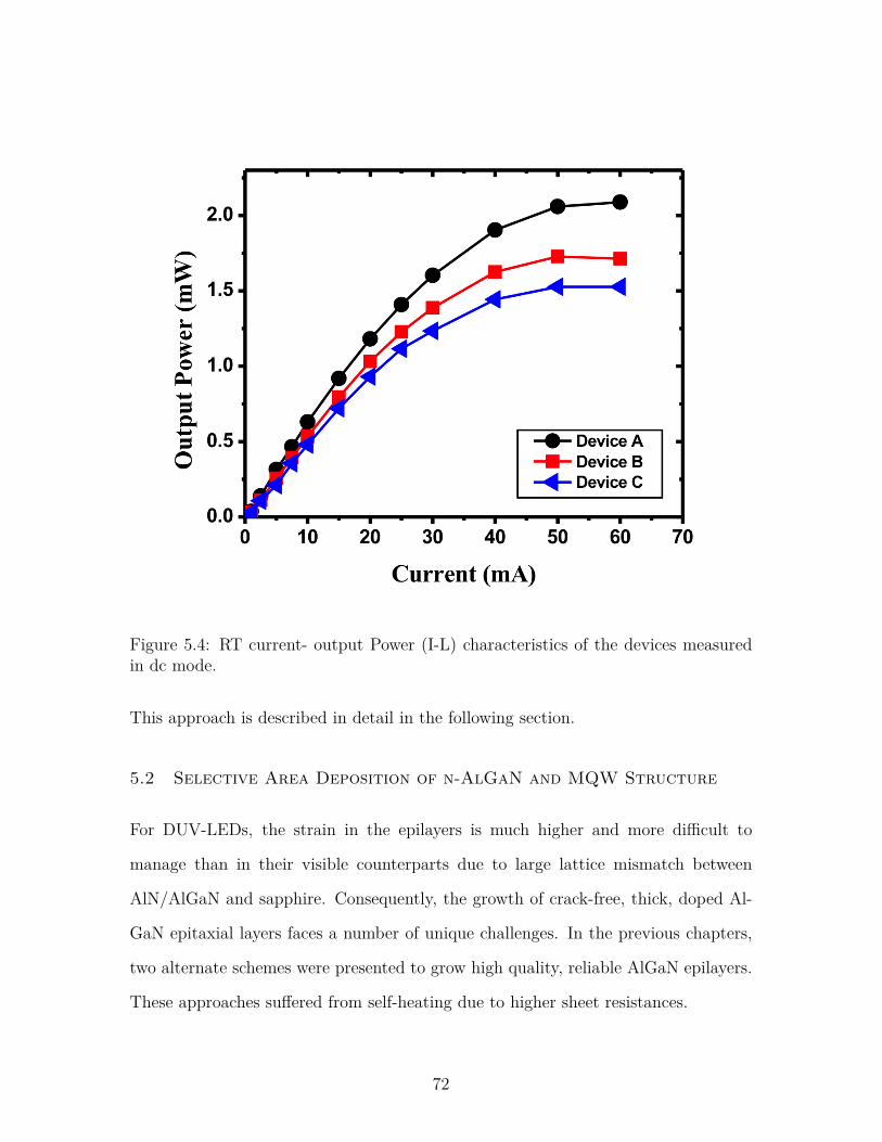
Figure 5.4: RT current- output Power (I-L) characteristics of the devices measuredin dc mode.
This approach is described in detail in the following section.
5.2 Selective Area Deposition of n-AlGaN and MQW Structure
For DUV-LEDs, the strain in the epilayers is much higher and more difficult to
manage than in their visible counterparts due to large lattice mismatch between
AlN/AlGaN and sapphire. Consequently, the growth of crack-free, thick, doped Al-
GaN epitaxial layers faces a number of unique challenges. In the previous chapters,
two alternate schemes were presented to grow high quality, reliable AlGaN epilayers.
These approaches suffered from self-heating due to higher sheet resistances.
72

(a) (b)
Figure 5.5: Schematic diagram of standard SPSL (left) and SAD (right) LEDs.
The outcome of the experiments in the last section revealed that any attempts to
reduce the sheet resistance by increasing the thickness of the epilayer result in higher
dislocation densities in these devices, hence impacting their EQE.
The selective area deposition technique has been used previously for deposition
of III-Nitride materials over silicon substrates [109]. This approach has been proven
to be effective in minimizing the micro-cracks formations by localizing the growth of
nitride epilayers.
In this section, the growth of n-AlGaN epilayers over sapphire substrate, using
selective area deposition, is presented. The schematic diagram of the selective area
deposited LEDs versus standard SPSL LEDs is shown in Figure 5.5.
Sample Preparation Process
A thin un-doped n-AlGaN layer is initially deposited on top of AlN/sapphire tem-
plate. Then 0.2-0.3 μm thick SiO2 mask pattern is transferred to this layer us-
ing plasma-enhanced chemical vapor deposition (PECVD), photolithography and
reactive-ion etching (RIE). The wafer is then thoroughly cleaned before loading it
in the MOCVD chamber for regrowth. The silicon doped n-AlGaN contact layer,
active region, p-AlGaN, p-GaN are selectively deposited in two steps. A step by step
73

(a) (b) (c)
Figure 5.6: Process-flow for selective area deposition (SAD) approach
Figure 5.7: AFM image of SAD n-AlGaN.
depiction of the entire process is shown in Figure 5.6.
Preliminary Results
The surface morphology for selective area deposited n-AlGaN is illustrated in Figure
5.7. A surface RMS of 0.203 nm is observed for SAD. which is comparable with RMS
value of 0.35 nm for conventionally grown n-AlGaN.
The electroluminescence spectrum for the LEDs grown with selective area de-
74

Figure 5.8: EL spectrum of SAD LEDs
position method, is plotted in Figure 5.8. For the first 2 growth runs, a shoulder
and longer wavelength emission bands were observed around 320 nm and 410 nm in
addition to the primary peak at approximately 275 nm.
After further optimizations in the electron blocking layer, the parasitic peak at 320
nm was eliminated and a much higher ratio of main to parasitic peaks was achieved,
as can be seen from the plot of wafer 3 in Figure 5.8.
The use of different metal schemes were investigated for the n-ohmic contacts. The
same metal stacks were evaporated on the n-AlGaN grown by selective area deposition
method and conventionally grown method. The results are shown in Figure 5.9. It is
evident from the plot that unetched SAD samples exhibit ohmic contacts with very
small barrier, as compared to the etched samples for the same metal stacks.
75
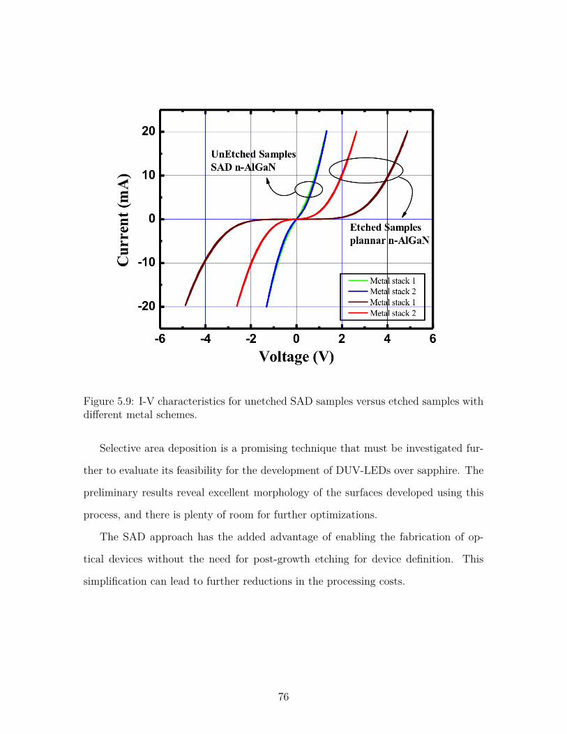
Figure 5.9: I-V characteristics for unetched SAD samples versus etched samples withdifferent metal schemes.
Selective area deposition is a promising technique that must be investigated fur-
ther to evaluate its feasibility for the development of DUV-LEDs over sapphire. The
preliminary results reveal excellent morphology of the surfaces developed using this
process, and there is plenty of room for further optimizations.
The SAD approach has the added advantage of enabling the fabrication of op-
tical devices without the need for post-growth etching for device definition. This
simplification can lead to further reductions in the processing costs.
76

Summary
In this chapter, it was shown that the sheet resistance of n-AlGaN decreases with
an increase in n-AlGaN thickness, but the optical output power does not follow this
trend. Beyond a certain threshold for thickness (2 μm for QPSM), the epilayers strain
is relieved in the form of dislocations. The increase in the crystal defects offsets any
advantages from a lower sheet resistance, resulting in a decline in the optical output
power of the device.
Selective area deposition technique is expected to decrease the dislocations den-
sity and enable the deposition of thick n-AlGaN, thereby improving both the material
crystal quality and conductivity. This technique has the potential to facilitate fabri-
cation of large area single chip DUV-LEDs due to the elimination of current crowding
by allowing the growth of thick n-AlGaN current spreading layers. Initial results are
promising for this approach but require further growth and processing optimization.
77

Chapter 6
Conclusions and Future Work
Due to their long life spans, robust nature, high efficiencies and low operating voltages,
light emitting diodes have emerged as an ideal candidate to dethrone the traditional
incandescent light bulb. Similarly, III-nitrides based light emitting diodes are poised
to completely replace bulky, fragile, environmentally hazardous UV mercury lamps.
In this research, a number of novel techniques have been proposed to improve the
reliability and output power of DUV-LEDs. In the following sections, the conclusions
derived from the outcome of the experiments are discussed and future directions for
further research are presented.
6.1 Conclusions
A major impediment to the development of commercially feasible DUV-LED is the
availability of a well-behaved native substrate that is both readily available and cost
effective. III-nitride light emitting diodes are generally grown on a sapphire substrate.
Sapphire substrates are inexpensive, abundant, and offer adequate transparency to
radiations down to 150 nm range. However, sapphire suffers from a number of serious
limitations. The large lattice mismatch between sapphire and AlN/AlGaN layers
creates high levels of strain in the epitaxial layer of the device. The resulting strain
reduces the likelihood of growing crack-free AlGaN layers.
Devices produced using a mismatched AlN/AlGaN layer on top of a sapphire
substrate often exhibit large number of dislocations. These defects lead to the creation
of non-radiative recombination centers for the injected carriers, lowering the overall
78

output power and efficiency of these device.
Short period superlattice structures have been successfully used to minimize and
mitigate the strain between the mismatched adjacent layers, allowing for the growth
of thick n-AlGaN layers. The fabrication of the superlattice structures is a complex
process that involves lengthy preparation and requires large amount of materials.
Furthermore, the growth of thick superlattice structures introduces bowing problems
for the resultant wafer. The bowing of the wafer introduces alignment problems
during the application of masks in the lithography process, which further reduces the
yield during fabrication.
In this dissertation, DUV-LEDs have been developed pseudomorphically on low
defect density AlN/sapphire template without the superlattice structures. This tech-
nique was initially introduced for bulk AlN substrates but its commercial applica-
tions are limited due to concerns related to the cost and availability of bulk AlN.
By replacing the bulk AlN with a high quality AlN/sapphire template, the overall
manufacturing cost of the resulting devices are significantly reduced while retaining
the many advantages offered by pseudomorphic layers.
For the first time, pseudomorphic DUV-LEDs have been fabricated with peak
emission wavelength of 275 nm. These devices exhibit better reliability scores as
compared to SPSL relaxed LEDs owing to the lower dislocation density in the pseu-
domorphically grown epitaxial layers.
The optical output power of pseudomorphic UV LEDs is observed to be lower
than standard UV LEDs with superlattice structures. The thickness of n-AlGaN
layer must be increased to reduce its sheet resistance and hence, increase its output
power. The maximum thickness that can be achieved in high-strain n-AlGaN layer
is limited in pseudomorphic LEDs. Increasing the thickness of the n-AlGaN layer
beyond a certain threshold significantly increases the dislocation density, reducing
the reliability as well as lowering the optical output power of the device.
79

To resolve the limitation of pseudomorphic LEDs, an alternate approach, based
on quasi-pseudomorphic n-AlGaN over AlN/sapphire, has also been developed in this
research. The thickness of n-AlGaN current spreading layer has been increased to 2
μm in the proposed approach as compared to the 0.6 μm for pseudomorphic LEDs.
The quasi-pseudomorphic LEDs have a partially relaxed structure compared to the
fully-strained structures in pseudomorphic LEDs. The reduced strain between the
adjacent layers allow for the growth of thicker n-AlGaN layers that can result in the
development of higher optical output devices. The optical output power achieved by
quasi-pseudomorphic LEDs, developed in this research, rivaled that of SPSL LEDs.
Device reliability, although lower than pseudomorphic LEDs, was considerably better
than standard superlattice LEDs, owing to the better epilayer crystal quality.
Comprehensive analysis of the devices revealed a ~25% drop in initial output
power for quasi-pseudomorphic versus ~35% for SPSL LEDs after 100 hours of con-
stant stress. The outcomes of these experiments have revealed the pseudomorphic
and quasi-pseudomorphic LEDs to be a serious contender to traditional, superlattice
based UV LEDs. These devices offer comparable output power and reliability with a
simpler growth and fabrication processes that can significantly reduce the unit cost
of DUV-LEDs for high volume production.
6.2 Future Work
A thicker n-AlGaN current spreading layer can mitigate the effects of current crowd-
ing, and can lead to the development of cost effective, large area, DUV-LEDs on a
single chip, without the need for intricate micro-pixel fabrication processes. Selec-
tive area deposition techniques for the growth of high quality thick n-AlGaN current
spreading layers have yielded promising preliminary results. Further research into se-
lective area deposition techniques and the optimization of the current pseudomorphic
and quasi-pseudomorphic growth schemes can result in the development of a wide
80
range of DUV-LEDs that can satisfy a wide range of reliability and output power
requirements.
81

Bibliography
[1] A. Khan, K. Balakrishnan, and T. Katona, “Ultraviolet light-emitting diodes
based on group three nitrides”, Nature photonics, vol. 2, no. 2, pp. 77–84, 2008.
[2] W. Morison, Phototherapy and Photochemotherapy of Skin Disease 2nd edn.
1991.
[3] N. Aeronautics and S. Administration. (). UV exposure has increased over the
last 30 years, but stabilized since the mid-1990s, [Online]. Available: http:
//www.nasa.gov/topics/solarsystem/features/uv-exposure.html.
[4] M. H. Crawford, M. A. Banas, M. P. Ross, D. S. Ruby, J. S. Nelson, R.
Boucher, and A. A. Allerman, “Final LDRD report: ultraviolet water purifica-
tion systems for rural environments and mobile applications”, Sandia Report,
2005. [Online]. Available: http : / / prod . sandia . gov / techlib / access -
control.cgi/2005/057245.pdf..
[5] S. Vilhunen, H. Särkkä, and M. Sillanpää, “Ultraviolet light-emitting diodes
in water disinfection”, Environmental Science and Pollution Research, vol. 16,
no. 4, pp. 439–442, 2009.
[6] M. Würtele, T. Kolbe, M. Lipsz, A. Külberg, M. Weyers, M. Kneissl, and
M. Jekel, “Application of GaN-based ultraviolet-C light emitting diodes–UV
LEDs–for water disinfection”, water research, vol. 45, no. 3, pp. 1481–1489,
2011.
[7] I. Sensor Electronic Technology. (). Product overview, [Online]. Available:
http://www.s-et.com/products.html.
82
[8] P. Sandvik, K. Mi, F. Shahedipour, R. McClintock, A. Yasan, P. Kung, and M.
Razeghi, “AlxGa1−xN for solar-blind UV detectors”, Journal of crystal growth,
vol. 231, no. 3, pp. 366–370, 2001.
[9] K. Davitt, Y.-K. Song, W. Patterson III, A. Nurmikko, M. Gherasimova, J.
Han, Y.-L. Pan, and R. Chang, “290 and 340 nm UV LED arrays for fluores-
cence detection from single airborne particles”, Optics express, vol. 13, no. 23,
pp. 9548–9555, 2005.
[10] A. Khan, Q. Fareed, and V. Adivarahan. (2010). Lamps boost output in the
deep ultraviolet, [Online]. Available: http://www.compoundsemiconductor.
net/article/86449-lamps-boost-output-in-the-deep-ultraviolet.
html.
[11] Y. Muramoto, M. Kimura, and S. Nouda, “Development and future of ultravi-
olet light-emitting diodes: UV-LED will replace the UV lamp”, Semiconductor
Science and Technology, vol. 29, no. 8, pp. 84 004–84 011, 2014.
[12] A. Khan and K. Balakrishnan, “Present status of deep UV nitride light emit-
ters”, in Materials Science Forum, Trans Tech Publ, vol. 590, 2008, pp. 141–
174.
[13] J. Pankove, E. Miller, and J. Berkeyheiser, “GaN electroluminescent diodes”,
in Electron Devices Meeting, 1971 International, IEEE, vol. 17, 1971, pp. 78–
78.
[14] H. Amano, N. Sawaki, I. Akasaki, and Y. Toyoda, “Metalorganic vapor phase
epitaxial growth of a high quality GaN film using an AlN buffer layer”, Applied
Physics Letters, vol. 48, no. 5, pp. 353–355, 1986.
[15] H. Amano, M. Kito, K. Hiramatsu, and I. Akasaki, “P-type conduction in
Mg-doped GaN treated with low-energy electron beam irradiation (LEEBI)”,
Japanese Journal of Applied Physics, vol. 28, no. 12A, p. L2112, 1989.
83

[16] S. Nakamura, “GaN growth using GaN buffer layer”, Japanese Journal of
Applied Physics, vol. 30, no. 10A, p. L1705, 1991.
[17] S. Nakamura, T. Mukai, M. Senoh, and N. Iwasa, “Thermal annealing effects
on p-type Mg-doped GaN films”, Japanese Journal of Applied Physics, vol. 31,
no. 2B, p. L139, 1992.
[18] S. Nakamura, M. Senoh, and T. Mukai, “High-power InGaN/GaN double-
heterostructure violet light emitting diodes”, Applied Physics Letters, vol. 62,
no. 19, pp. 2390–2392, 1993.
[19] S. Nakamura, M. Senoh, N. Iwasa, and S.-i. Nagahama, “High-power InGaN
single-quantum-well-structure blue and violet light-emitting diodes”, Applied
Physics Letters, vol. 67, no. 13, pp. 1868–1870, 1995.
[20] S. Nakamura, M. Senoh, S.-i. Nagahama, N. Iwasa, T. Yamada, T. Mat-
sushita, H. Kiyoku, and Y. Sugimoto, “InGaN multi-quantum-well-structure
laser diodes with cleaved mirror cavity facets”, Japanese journal of applied
physics, vol. 35, no. 2B, p. L217, 1996.
[21] S. Nakamura, M. Senoh, S.-i. Nagahama, N. Iwasa, T. Yamada, T. Matsushita,
Y. Sugimoto, and H. Kiyoku, “Room-temperature continuous-wave operation
of InGaN multi-quantum-well structure laser diodes”, Applied Physics Letters,
vol. 69, no. 26, pp. 4056–4058, 1996.
[22] M. Krames, O. Shchekin, R. Mueller-Mach, G. O. Mueller, L. Zhou, G. Har-
bers, and M. Craford, “Status and future of high-power light-emitting diodes
for solid-state lighting”, Display Technology, Journal of, vol. 3, no. 2, pp. 160–
175, Jun. 2007, issn: 1551-319X. doi: 10.1109/JDT.2007.895339.
[23] M. A. Khan, R. Skogman, J. Van Hove, S. Krishnankutty, and R. Kolbas,
“Photoluminescence characteristics of AlGaN-GaN-AlGaN quantum wells”,
Applied physics letters, vol. 56, no. 13, pp. 1257–1259, 1990.
84

[24] J. Han, M. Crawford, R. Shul, J. Figiel, M. Banas, L. Zhang, Y. Song, H.
Zhou, and A. Nurmikko, “AlGaN/GaN quantum well ultraviolet light emitting
diodes”, Applied physics letters, vol. 73, no. 12, pp. 1688–1690, 1998.
[25] T. Nishida and N. Kobayashi, “346 nm emission from AlGaN multi-quantum-
well light emitting diode”, physica status solidi (a), vol. 176, no. 1, pp. 45–48,
1999.
[26] M. A. Khan, J. Yang, G. Simin, R. Gaska, M. Shur, H.-C. zur Loye, G. Tamu-
laitis, A. Zukauskas, D. J. Smith, D. Chandrasekhar, et al., “Lattice and energy
band engineering in AlInGaN/GaN heterostructures”, Applied Physics Letters,
vol. 76, no. 9, pp. 1161–1163, 2000.
[27] V. Adivarahan, A. Chitnis, J. Zhang, M. Shatalov, J. Yang, G. Simin, M. A.
Khan, R. Gaska, and M. Shur, “Ultraviolet light-emitting diodes at 340 nm
using quaternary AlInGaN multiple quantum wells”, Applied Physics Letters,
vol. 79, no. 25, pp. 4240–4242, 2001.
[28] A. Kinoshita, H. Hirayama, M. Ainoya, Y. Aoyagi, and A. Hirata, “Room-
temperature operation at 333 nm of Al0.03Ga0.97N/Al0.25Ga0.75N quantum-well
light-emitting diodes with Mg-doped superlattice layers”, Applied Physics Let-
ters, vol. 77, no. 2, pp. 175–177, 2000.
[29] M. A. Khan, V. Adivarahan, J. P. Zhang, C. Chen, E. Kuokstis, A. Chitnis,
M. Shatalov, J. W. Yang, and G. Simin, “Stripe geometry ultraviolet light
emitting diodes at 305 nanometers using quaternary AlInGaN multiple quan-
tum wells”, Japanese Journal of Applied Physics, vol. 40, no. 12A, p. L1308,
2001.
[30] V. Adivarahan, S. Wu, A. Chitnis, R. Pachipulusu, V. Mandavilli, M. Shat-
alov, J. Zhang, M. A. Khan, G. Tamulaitis, A. Sereika, et al., “AlGaN single-
85
quantum-well light-emitting diodes with emission at 285 nm”, Applied Physics
Letters, vol. 81, no. 19, pp. 3666–3668, 2002.
[31] J. Zhang, A. Chitnis, V. Adivarahan, S. Wu, V. Mandavilli, R. Pachipulusu,
M. Shatalov, G. Simin, J. Yang, and M. A. Khan, “Milliwatt power deep ultra-
violet light-emitting diodes over sapphire with emission at 278 nm”, Applied
physics letters, vol. 81, no. 26, pp. 4910–4912, 2002.
[32] K. Mayes, A. Yasan, R. McClintock, D. Shiell, S. Darvish, P. Kung, and M.
Razeghi, “High-power 280 nm AlGaN light-emitting diodes based on an asym-
metric single-quantum well”, Applied physics letters, vol. 84, no. 7, pp. 1046–
1048, 2004.
[33] A. Fujioka, T. Misaki, T. Murayama, Y. Narukawa, and T. Mukai, “Improve-
ment in output power of 280-nm deep ultraviolet light-emitting diode by using
AlGaN multi quantum wells”, Applied physics express, vol. 3, no. 4, p. 041 001,
2010.
[34] Y. Liao, C. Thomidis, C.-k. Kao, and T. D. Moustakas, “AlGaN based deep
ultraviolet light emitting diodes with high internal quantum efficiency grown
by molecular beam epitaxy”, Applied Physics Letters, vol. 98, no. 8, p. 081 110,
2011.
[35] Y. Taniyasu, M. Kasu, and T. Makimoto, “An aluminium nitride light-emitting
diode with a wavelength of 210 nanometres”, Nature, vol. 441, no. 7091,
pp. 325–328, 2006.
[36] N. Otsuka, A. Tsujimura, Y. Hasegawa, G. Sugahara, M. Kume, and Y. Ban,
“Room temperature 339 nm emission from Al0.13Ga0.87N/Al0.10Ga0.90 double
heterostructure light-emitting diode on sapphire substrate”, Japanese Journal
of Applied Physics, vol. 39, no. 5B, p. L445, 2000.
86

[37] A. Chitnis, J. Zhang, V. Adivarahan, M. Shatalov, S. Wu, R. Pachipulusu,
V. Mandavilli, and M. A. Khan, “Improved performance of 325-nm emission
AlGaN ultraviolet light-emitting diodes”, Applied physics letters, vol. 82, no.
16, pp. 2565–2567, 2003.
[38] K. Lee, P. Parbrook, T. Wang, J. Bai, F. Ranalli, R. Airey, and G. Hill, “Effect
of the AlGaN electron blocking layer thickness on the performance of AlGaN-
based ultraviolet light-emitting diodes”, Journal of Crystal Growth, vol. 311,
no. 10, pp. 2857–2859, 2009.
[39] E. F. Schubert, T. Gessmann, and J. K. Kim, Light emitting diodes. Wiley
Online Library, 2005.
[40] C. Pernot, M. Kim, S. Fukahori, T. Inazu, T. Fujita, Y. Nagasawa, A. Hirano,
M. Ippommatsu, M. Iwaya, S. Kamiyama, et al., “Improved efficiency of 255-
280 nm AlGaN-based light-emitting diodes”, Applied physics express, vol. 3,
no. 6, p. 061 004, 2010.
[41] T. Fujii, Y. Gao, R. Sharma, E. Hu, S. DenBaars, and S. Nakamura, “Increase
in the extraction efficiency of GaN-based light-emitting diodes via surface
roughening”, Applied physics letters, vol. 84, no. 6, pp. 855–857, 2004.
[42] O. Shchekin, J. Epler, T. Trottier, T. Margalith, D. Steigerwald, M. Holcomb,
P. Martin, and M. Krames, “High performance thin-film flip-chip InGaN-GaN
light-emitting diodes”, Applied Physics Letters, vol. 89, no. 7, pp. 071 109–
071 109, 2006.
[43] R.-H. Horng, H.-L. Hu, M.-T. Chu, Y.-L. Tsai, Y.-J. Tsai, C.-P. Hsu, and D.-S.
Wuu, “Performance of flip-chip thin-film GaN light-emitting diodes with and
without patterned sapphires”, Photonics Technology Letters, IEEE, vol. 22,
no. 8, pp. 550–552, 2010.
87
[44] H. Aoshima, K. Takeda, K. Takehara, S. Ito, M. Mori, M. Iwaya, T. Takeuchi,
S. Kamiyama, I. Akasaki, and H. Amano, “Laser lift-off of AlN/sapphire for
UV light-emitting diodes”, physica status solidi (c), vol. 9, no. 3-4, pp. 753–
756, 2012.
[45] P. Dong, J. Yan, J. Wang, Y. Zhang, C. Geng, T. Wei, P. Cong, Y. Zhang,
J. Zeng, Y. Tian, et al., “282-nm AlGaN-based deep ultraviolet light-emitting
diodes with improved performance on nano-patterned sapphire substrates”,
Applied Physics Letters, vol. 102, no. 24, p. 241 113, 2013.
[46] M. Shatalov, A. Lunev, X. Hu, O. Bilenko, I. Gaska, W. Sun, J. Yang, A.
Dobrinsky, Y. Bilenko, R. Gaska, et al., “Performance and applications of
deep UV LED”, International Journal of High Speed Electronics and Systems,
vol. 21, no. 01, 2012.
[47] X. Hu, J. Deng, J. Zhang, A. Lunev, Y. Bilenko, T. Katona, M. Shur, R.
Gaska, M. Shatalov, and A. Khan, “Deep ultraviolet light-emitting diodes”,
physica status solidi (a), vol. 203, no. 7, pp. 1815–1818, 2006.
[48] W. Sun, M. Shatalov, J. Deng, X. Hu, J. Yang, A. Lunev, Y. Bilenko, M. Shur,
and R. Gaska, “Efficiency droop in 245-247 nm AlGaN light-emitting diodes
with continuous wave 2 mW output power”, Applied Physics Letters, vol. 96,
no. 6, p. 061 102, 2010.
[49] H. Hirayama, Y. Tsukada, T. Maeda, and N. Kamata, “Marked enhancement
in the efficiency of deep-ultraviolet AlGaN light-emitting diodes by using a
multiquantum-barrier electron blocking layer”, Applied Physics Express, vol.
3, no. 3, p. 031 002, 2010.
[50] M. Kneissl, T. Kolbe, C. Chua, V. Kueller, N. Lobo, J. Stellmach, A. Knauer,
H. Rodriguez, S. Einfeldt, Z. Yang, et al., “Advances in group III-nitride-
88
based deep UV light-emitting diode technology”, Semiconductor Science and
Technology, vol. 26, no. 1, p. 014 036, 2011.
[51] C. Sun, P. Kung, A. Saxler, H. Ohsato, K. Haritos, and M. Razeghi, “A crys-
tallographic model of (00.1) aluminum nitride epitaxial thin film growth on
(00.1) sapphire substrate”, Journal of applied physics, vol. 75, no. 8, pp. 3964–
3967, 1994.
[52] T. Kolbe, Private communication, 2010.
[53] J. Zhang, H. Wang, M. Gaevski, C. Chen, Q. Fareed, J. Yang, G. Simin, and
M. Asif Khan, “Crack-free thick AlGaN grown on sapphire using AlN/AlGaN
superlattices for strain management”, Applied physics letters, vol. 80, no. 19,
pp. 3542–3544, 2002.
[54] H.-M. Wang, J.-P. Zhang, C.-Q. Chen, Q. Fareed, J.-W. Yang, and M. A.
Khan, “AlN/AlGaN superlattices as dislocation filter for low threading dislo-
cation thick AlGaN layers on sapphire”, Applied physics letters, vol. 81, no. 4,
pp. 604–606, 2002.
[55] J. Zhang, X. Hu, A. Lunev, J. Deng, Y. Bilenko, T. M. Katona, M. S. Shur,
R. Gaska, and M. A. Khan, “AlGaN deep-ultraviolet light-emitting diodes”,
Japanese journal of applied physics, vol. 44, no. 10R, p. 7250, 2005.
[56] C. Pernot, S. Fukahori, T. Inazu, T. Fujita, M. Kim, Y. Nagasawa, A. Hirano,
M. Ippommatsu, M. Iwaya, S. Kamiyama, et al., “Development of high effi-
ciency 255-355 nm AlGaN-based light-emitting diodes”, physica status solidi
(a), vol. 208, no. 7, pp. 1594–1596, 2011.
[57] H. Hirayama, T. Yatabe, N. Noguchi, T. Ohashi, and N. Kamata, “231-261
nm AlGaN deep-ultraviolet light-emitting diodes fabricated on AlN multilayer
buffers grown by ammonia pulse-flow method on sapphire”, Applied Physics
Letters, vol. 91, no. 7, pp. 071 901–071 901, 2007.
89

[58] H. Hirayama, S. Fujikawa, N. Noguchi, J. Norimatsu, T. Takano, K. Tsubaki,
and N. Kamata, “222-282 nm AlGaN and InAlGaN-based deep-UV LEDs
fabricated on high-quality AlN on sapphire”, physica status solidi (a), vol.
206, no. 6, pp. 1176–1182, 2009.
[59] F. Brunner, H. Protzmann, M. Heuken, A. Knauer, M. Weyers, and M. Kneissl,
“High-temperature growth of AlN in a production scale 11 × 2’ MOVPE
reactor”, physica status solidi (c), vol. 5, no. 6, pp. 1799–1801, 2008.
[60] W. Sun, J. Zhang, J. Yang, H. Maruska, M. Asif Khan, R. Liu, and F.
Ponce, “Fine structure of AlN/AlGaN superlattice grown by pulsed atomic-
layer epitaxy for dislocation filtering”, Applied Physics Letters, vol. 87, no. 21,
pp. 211 915–211 915, 2005.
[61] I. Ahmad, B. Krishnan, B. Zhang, Q. Fareed, M. Lachab, J. Dion, and A.
Khan, “Dislocation reduction in high Al-content AlGaN films for deep ultravi-
olet light emitting diodes”, physica status solidi (a), vol. 208, no. 7, pp. 1501–
1503, 2011.
[62] J. Yan, J. Wang, P. Cong, L. Sun, N. Liu, Z. Liu, C. Zhao, and J. Li, “Improved
performance of UV-LED by p-AlGaN with graded composition”, physica status
solidi (c), vol. 8, no. 2, pp. 461–463, 2011.
[63] L. Zhou, J. Epler, M. Krames, W. Goetz, M. Gherasimova, Z. Ren, J. Han, M.
Kneissl, and N. Johnson, “Vertical injection thin-film AlGaN/AlGaN multiple-
quantum-well deep ultraviolet light-emitting diodes”, Applied physics letters,
vol. 89, no. 24, pp. 241 113–241 113, 2006.
[64] V. Adivarahan, A. Heidari, B. Zhang, Q. Fareed, M. Islam, S. Hwang, K.
Balakrishnan, and A. Khan, “Vertical injection thin film deep ultraviolet light
emitting diodes with AlGaN multiple-quantum wells active region”, Applied
physics express, vol. 2, no. 9, p. 092 102, 2009.
90
[65] S. Hwang, D. Morgan, A. Kesler, M. Lachab, B. Zhang, A. Heidari, H. Nazir,
I. Ahmad, J. Dion, Q. Fareed, et al., “276 nm substrate-free flip-chip AlGaN
light-emitting diodes”, Applied physics express, vol. 4, no. 3, p. 032 102, 2011.
[66] F. Asif, H.-C. Chen, A. Coleman, M. Lachab, I. Ahmad, B. Zhang, Q. Fareed,
V. Adivarahan, and A. Khan, “Substrate lifted-off AlGaN/AlGaN lateral con-
duction thin-film light-emitting diodes operating at 285 nm”, Japanese Journal
of Applied Physics, vol. 52, no. 8S, 08JG14, 2013.
[67] M. Lachab, F. Asif, B. Zhang, I. Ahmad, A. Heidari, Q. Fareed, V. Adivara-
han, and A. Khan, “Enhancement of light extraction efficiency in sub-300nm
nitride thin-film flip-chip light-emitting diodes”, Solid-State Electronics, vol.
89, pp. 156–160, 2013.
[68] N. Lobo, H. Rodriguez, A. Knauer, M. Hoppe, S. Einfeldt, P. Vogt, M. Weyers,
and M. Kneissl, “Enhancement of light extraction in ultraviolet light-emitting
diodes using nanopixel contact design with Al reflector”, Applied Physics Let-
ters, vol. 96, no. 8, p. 081 109, 2010.
[69] M. Shatalov, W. Sun, A. Lunev, X. Hu, A. Dobrinsky, Y. Bilenko, J. Yang, M.
Shur, R. Gaska, C. Moe, et al., “AlGaN deep-ultraviolet light-emitting diodes
with external quantum efficiency above 10%”, Applied Physics Express, vol. 5,
no. 8, p. 082 101, 2012.
[70] S. Nakamura, “The roles of structural imperfections in InGaN-based blue light-
emitting diodes and laser diodes”, Science, vol. 281, no. 5379, pp. 956–961,
1998.
[71] V. Adivarahan, A. Heidari, B. Zhang, Q. Fareed, S. Hwang, M. Islam, and
A. Khan, “280 nm deep ultraviolet light emitting diode lamp with an AlGaN
multiple quantum well active region”, Applied Physics Express, vol. 2, no. 10,
p. 102 101, 2009.
91
[72] M. Shatalov, J. Yang, W. Sun, R. Kennedy, R. Gaska, K. Liu, M. Shur, and
G. Tamulaitis, “Efficiency of light emission in high aluminum content AlGaN
quantum wells”, Journal of Applied Physics, vol. 105, no. 7, p. 073 103, 2009.
[73] M. A. Khan, “AlGaN multiple quantum well based deep UV LEDs and their
applications”, physica status solidi (a), vol. 203, no. 7, pp. 1764–1770, 2006.
[74] S. G. Mueller, R. T. Bondokov, K. E. Morgan, G. A. Slack, S. B. Schujman,
J. Grandusky, J. A. Smart, and L. J. Schowalter, “The progress of AlN bulk
growth and epitaxy for electronic applications”, physica status solidi (a), vol.
206, no. 6, pp. 1153–1159, 2009.
[75] R. Dalmau, B. Moody, R. Schlesser, S. Mita, J. Xie, M. Feneberg, B. Neuschl,
K. Thonke, R. Collazo, A. Rice, et al., “Growth and characterization of AlN
and AlGaN epitaxial films on AlN single crystal substrates”, Journal of The
Electrochemical Society, vol. 158, no. 5, H530–H535, 2011.
[76] L. Schowalter, S. Schujman, W. Liu, M. Goorsky, M. Wood, J. Grandusky, and
F. Shahedipour-Sandvik, “Development of native, single crystal AlN substrates
for device applications”, physica status solidi (a), vol. 203, no. 7, pp. 1667–
1671, 2006.
[77] J. R. Grandusky, J. Chen, S. R. Gibb, M. C. Mendrick, C. G. Moe, L. Ro-
dak, G. A. Garrett, M. Wraback, and L. J. Schowalter, “270 nm pseudomor-
phic ultraviolet light-emitting diodes with over 60 mw continuous wave output
power”, Applied Physics Express, vol. 6, no. 3, p. 032 101, 2013.
[78] T. Kinoshita, T. Obata, T. Nagashima, H. Yanagi, B. Moody, S. Mita, S.-i.
Inoue, Y. Kumagai, A. Koukitu, and Z. Sitar, “Performance and reliability
of deep-ultraviolet light-emitting diodes fabricated on AlN substrates pre-
pared by hydride vapor phase epitaxy”, Applied Physics Express, vol. 6, no. 9,
p. 092 103, 2013.
92
[79] G. Miller, D. Robinson, and J. Wiley, “Contactless measurement of semicon-
ductor conductivity by radio frequency-free-carrier power absorption”, Review
of Scientific Instruments, vol. 47, no. 7, pp. 799–805, 1976.
[80] B. I. for Advanced Science and T. U. of Illinois at Urbana-Champaign. ().
Scanning probe microscopy, [Online]. Available: http://virtual.itg.uiuc.
edu/training/AFM_tutorial/.
[81] U. O. S. Florida. (). Thin films, [Online]. Available: http://www.eng.usf.
edu/~tvestgaa/ThinFilm/.
[82] N. A. Geisse, “AFM and combined optical techniques”, Materials today, vol.
12, no. 7, pp. 40–45, 2009.
[83] MIT. (). Xray diffraction, [Online]. Available: http://prism.mit.edu/xray/.
[84] J. A. Dion, “Reduced defect density nAlGaN template layer for improved
output deep-UV LED”, PhD thesis, UNIVERSITY OF SOUTH CAROLINA,
2011.
[85] W. Sun, V. Adivarahan, M. Shatalov, Y. Lee, S. Wu, J. Yang, J. Zhang, and
M. A. Khan, “Continuous wave milliwatt power AlGaN light emitting diodes
at 280 nm”, Japanese journal of applied physics, vol. 43, no. 11A, p. L1419,
2004.
[86] M. Shatalov, W. Sun, Y. Bilenko, A. Sattu, X. Hu, J. Deng, J. Yang, M.
Shur, C. Moe, M. Wraback, et al., “Large chip high power deep ultraviolet
light-emitting diodes”, Applied physics express, vol. 3, no. 6, p. 062 101, 2010.
[87] J. Grandusky, J. Smart, M. Mendrick, L. Schowalter, K. Chen, and E. Schu-
bert, “Pseudomorphic growth of thick n-type AlxGa1−xN layers on low-defect-
density bulk AlN substrates for UV LED applications”, Journal of Crystal
Growth, vol. 311, no. 10, pp. 2864–2866, 2009.
93
[88] J. Matthews and A. Blakeslee, “Defects in epitaxial multilayers: i. misfit dis-
locations”, Journal of Crystal Growth, vol. 27, pp. 118–125, 1974.
[89] M. Shatalov, M. Gaevski, V. Adivarahan, and A. Khan, “Room-temperature
stimulated emission from AlN at 214 nm”, Japanese journal of applied physics,
vol. 45, no. 12L, p. L1286, 2006.
[90] T. Wunderer, C. Chua, J. Northrup, Z. Yang, N. Johnson, M. Kneissl, G.
Garrett, H. Shen, M. Wraback, B. Moody, et al., “Optically pumped uv
lasers grown on bulk AlN substrates”, physica status solidi (c), vol. 9, no.
3-4, pp. 822–825, 2012.
[91] J. Xie, S. Mita, Z. Bryan, W. Guo, L. Hussey, B. Moody, R. Schlesser, R.
Kirste, M. Gerhold, R. Collazo, et al., “Lasing and longitudinal cavity modes
in photo-pumped deep ultraviolet AlGaN heterostructures”, Applied Physics
Letters, vol. 102, no. 17, p. 171 102, 2013.
[92] Z. Lochner, T.-T. Kao, Y.-S. Liu, X.-H. Li, M. M. Satter, S.-C. Shen, P. D.
Yoder, J.-H. Ryou, R. D. Dupuis, Y. Wei, et al., “Deep-ultraviolet lasing at
243 nm from photo-pumped AlGaN/AlN heterostructure on AlN substrate”,
Applied Physics Letters, vol. 102, no. 10, p. 101 110, 2013.
[93] V. Jmerik, E. Lutsenko, and S. Ivanov, “Plasma-assisted molecular beam epi-
taxy of AlGaN heterostructures for deep-ultraviolet optically pumped lasers”,
physica status solidi (a), vol. 210, no. 3, pp. 439–450, 2013.
[94] M. Martens, F. Mehnke, C. Kuhn, C. Reich, V. Kueller, A. Knauer, C. Netzel,
C. Hartmann, J. Wollweber, J. Rass, T. Wernicke, M. Bickermann, M. Weyers,
and M. Kneissl, “Performance characteristics of UV-C AlGaN-based lasers
grown on sapphire and bulk AlN substrates”, Photonics Technology Letters,
IEEE, vol. 26, no. 4, pp. 342–345, Feb. 2014, issn: 1041-1135. doi: 10.1109/
LPT.2013.2293611.
94

[95] M. Lachab, F. Asif, A. Coleman, I. Ahmad, B. Zhang, V. Adivarahan, and
A. Khan, “Optically-pumped 285 nm edge stimulated emission from AlGaN-
based led structures grown by MOCVD on sapphire substrates”, Japanese
Journal of Applied Physics, vol. 53, no. 11, p. 112 101, 2014.
[96] S. M. Sze and K. K. Ng, Physics of semiconductor devices. John Wiley & Sons,
2006.
[97] D. Brunner, H. Angerer, E. Bustarret, F. Freudenberg, R. Hopler, R. Dimitrov,
O. Ambacher, and M. Stutzmann, “Optical constants of epitaxial AlGaN films
and their temperature dependence”, Journal of applied physics, vol. 82, no. 10,
pp. 5090–5096, 1997.
[98] S. Ivanov, D. Nechaev, A. Sitnikova, V. Ratnikov, M. Yagovkina, N. Rzheut-
skii, E. Lutsenko, and V. Jmerik, “Plasma-assisted molecular beam epitaxy
of Al(Ga)N layers and quantum well structures for optically pumped mid-
UV lasers on c-Al2O3”, Semiconductor Science and Technology, vol. 29, no. 8,
p. 084 008, 2014.
[99] R. Banal, M. Funato, and Y. Kawakami, “Optical anisotropy in [0001]-oriented
Alx Ga1−xN/AlN quantum wells (x>0.69)”, Physical Review B, vol. 79, no. 12,
p. 121 308, 2009.
[100] J. Northrup, C. Chua, Z. Yang, T. Wunderer, M. Kneissl, N. Johnson, and
T. Kolbe, “Effect of strain and barrier composition on the polarization of light
emission from AlGaN/AlN quantum wells”, Applied Physics Letters, vol. 100,
no. 2, p. 021 101, 2012.
[101] H.-C. Chen, I. Ahmad, B. Zhang, A. Coleman, M. Sultana, V. Adivarahan, and
A. Khan, “Pulsed modulation doping of AlxGa1−xN (x>0.6) AlGaN epilayers
for deep UV optoelectronic devices”, physica status solidi (c), vol. 11, no. 3-4,
pp. 408–411, 2014.
95
[102] S. Wu, S. Chhajed, L. Yan, W. Sun, M. Shatalov, V. Adivarahan, and M. A.
Khan, “Matrix addressable micro-pixel 280 nm deep UV light-emitting diodes”,
Japanese journal of applied physics, vol. 45, no. 4L, p. L352, 2006.
[103] M. Shatalov, A. Chitnis, V. Mandavilli, R. Pachipulusu, J. Zhang, V. Adi-
varahan, S. Wu, G. Simin, M. A. Khan, G. Tamulaitis, et al., “Time-resolved
electroluminescence of AlGaN-based light-emitting diodes with emission at
285 nm”, Applied physics letters, vol. 82, no. 2, pp. 167–169, 2003.
[104] A. Khan, S. Hwang, J. Lowder, V. Adivarahan, and Q. Fareed, “Reliability
issues in AlGaN based deep ultraviolet light emitting diodes”, in Reliability
Physics Symposium, 2009 IEEE International, IEEE, 2009, pp. 89–93.
[105] J. Grandusky, Y. Cui, S. Gibb, M. Mendrick, and L. Schowalter, “Performance
and reliability of ultraviolet-C pseudomorphic light emitting diodes on bulk
AlN substrates”, physica status solidi (c), vol. 7, no. 7-8, pp. 2199–2201, 2010.
[106] Z. Gong, M. Gaevski, V. Adivarahan, W. Sun, M. Shatalov, and M. Asif
Khan, “Optical power degradation mechanisms in AlGaN-based 280 nm deep
ultraviolet light-emitting diodes on sapphire”, Applied physics letters, vol. 88,
no. 12, pp. 121 106–121 106, 2006.
[107] A. Pinos, S. Marcinkevičius, J. Yang, R. Gaska, M. Shatalov, and M. Shur,
“Optical studies of degradation of AlGaN quantum well based deep ultraviolet
light emitting diodes”, Journal of Applied Physics, vol. 108, no. 9, p. 093 113,
2010.
[108] M. Shatalov, Z. Gong, M. Gaevski, S. Wu, W. Sun, V. Adivarahan, and M. A.
Khan, “Reliability of AlGaN-based deep UV LEDs on sapphire”, in Integrated
Optoelectronic Devices 2006, International Society for Optics and Photonics,
2006, 61340P–61340P.
96
[109] J. Yang, A. Lunev, G. Simin, A. Chitnis, M. Shatalov, M. A. Khan, J. E. Van
Nostrand, and R. Gaska, “Selective area deposited blue GaN-InGaN multiple-
quantum well light emitting diodes over silicon substrates”, Applied Physics
Letters, vol. 76, no. 3, pp. 273–275, 2000.
97

Appendix A
Permission to Reprint
98

99