design, hardware implementation and control of a 3-phase ... · design, hardware implementation and...
TRANSCRIPT

Design, Hardware implementation and
Control of a 3-phase, 3-level Unity Power
Factor Rectifier
A Project Report
Submitted in Partial Fulfilment of
Requirement for the Degree of
Master of Engineeringin
Electrical Engineering
By
Krishna Kumar M J
Department of Electrical Engineering
Indian Institute of Science
Bangalore - 560 012
India
June 2012

Acknowledgements
I feel fortunate to have done my M.E project with Dr. Vinod John as my project guide. I
thank him for letting me work on this challenging and thought provoking project through
which I have been able to gain valuable knowledge and insight about the working of power
electronic systems. His timely and valuable suggestions on solving the problems that I en-
countered during project work or whenever I was stuck have been extremely helpful through-
out the project time-line. I am thankful for his constant interest in my work and encourage-
ment. His organised way of getting things done has been a constant source of inspiration for
me. The course on ‘Topics in Power Electronics and Distributed Generation’ taught by him
gave me a new perspective about the analysis and design of power electronic systems.
I thank Prof. G Narayanan whole heartedly for his excellent teaching of Power electronics,
Electric drives and PWM courses. The insight he offered in each of his lectures made his
courses very interesting. His lab courses helped a great deal in getting hands on experience
on hardware equipment and knowing about the multiple problems that one can encounter
while working on practical systems.
I thank Dr. Joy Thomas of HVE and Dr. G.V. Mahesh of CEDT for their knowledge-
able, insightful and practically oriented courses on HV Engineering and Electronic systems
packaging respectively.
I thank all the professors at IISc who have taught and shared their valuable expertise
with me.
I thank my friends Rajendra Prasad (RP), Amit, Akshay, Vikash, Arun for the fruitful
discussions on academic and non-academic subjects ranging over a variety of topics. I thank
my friends Saichand, Vamshi, Satish, Gopal and other members of the badminton gang for
their support and the all the fun we have had during those badminton games. I thank
Sudarshan and Anand for the various discussions we have had and also for their help on
i

ii Acknowledgements
various computer issues. A special thanks goes out to the A-mess group who have been a
constant source of support throughout the duration of my stay at IISc. I thank all my M.E
friends for helping me in one way or the other.
I thank Abhijit and all members of the PEG for the useful academic discussions I have
had with them and for the valuable inputs received from them. I am thankful to all my M.E
seniors for their warmth, help and academic inputs.
I thank the members of workshop especially Mr. Ramachandra and Mr. Ravi for their
timely help in my project. I thank Silvi madam for her kind help. I thank Mr. H.N
Purushottam, Mr. D.M Channegowda, Mr.Kini for providing excellent administrative help.
I thank the authorities, cooks and workers of A-mess for providing nutritious/good food
and ambience. I thank the administration of IISc and the hostel authorities for providing
me with good accomodation. I thank the doctors at the health centre for helping me stay
in good health throughout my course duration.
I thank MHRD for its financial assistance.
All the credit for everything good in me goes to my family. Their constant encouragement,
love and faith in me is the main reason for what I am or for what I have achieved till this
day. I thank them for standing by my side and supporting me at all times.
I thank all my past teachers, and finally I thank the all-powerful supreme being for giving
me strength at all times.
Abstract
Usage of conventional bridge type rectifiers for obtaining DC power from AC grid results
in injection of unwanted current harmonics into the grid. Due to standards such as IEEE
519-1992 [1] which limit the amount of harmonic injection into the mains, the bridge type
rectifiers are being replaced by improved power quality converters which have reduced har-
monic injection into the mains along with a host of other advantages.
This project deals with the hardware development and control of a 3-phase, 3-level UPF
rectifier which is a variant of an improved power quality converter named vienna rectifier [2].
The 3-phase, 3-level rectifier is characterised by its input currents being almost sinusoidal,
reduced input current ripple, controllable output DC voltage, high power density and UPF
operation. Further, reduced losses and a lesser component count of the 3-phase, 3-level
rectifier compared to the vienna rectifier indicate a greater scope for reduction in the size of
the rectifier along with reduced packaging effort.
In this work, the necessary hardware for the 3-phase, 3-level UPF rectifier has been
developed, assembled and tested for a power level of 2kW and a DC bus voltage of 750V.
A carrier based control strategy has been proposed for the control of the rectifier and its
operation is validated on the hardware setup. Based on the results obtained from simulation
and hardware implementation, a comparison has been done between the already existing
hysteresis based control strategy [2] and the proposed carrier based control strategy.
Overall, the project work involves the building of the 3-phase, 3-level UPF rectifier setup,
design of the controller parameters, validation of the proposed carrier based control strat-
egy both in simulation/hardware and comparison of the proposed control strategy with an
originally existing hysteresis based control strategy.
iii

Contents
Acknowledgements i
Abstract iii
List of Tables vii
List of Figures viii
Nomenclature xi
1 Introduction 1
1.1 Project Work . . . . . . . . . . . . . . . . . . . . . . . . . . . . . . . . . . . 2
1.2 Organization of the thesis . . . . . . . . . . . . . . . . . . . . . . . . . . . . 3
2 Operating Principle of the 3-phase, 3-level Rectifier 5
2.1 Three level characteristic . . . . . . . . . . . . . . . . . . . . . . . . . . . . . 5
2.2 Basic functionality . . . . . . . . . . . . . . . . . . . . . . . . . . . . . . . . 5
3 Hardware Design 8
3.1 Specifications of the 3-phase, 3-level rectifier . . . . . . . . . . . . . . . . . . 8
3.2 Device selection . . . . . . . . . . . . . . . . . . . . . . . . . . . . . . . . . . 9
3.3 Capacitor Design . . . . . . . . . . . . . . . . . . . . . . . . . . . . . . . . . 10
3.3.1 Capacitor ripple current calculation . . . . . . . . . . . . . . . . . . . 11
3.4 Inductor design . . . . . . . . . . . . . . . . . . . . . . . . . . . . . . . . . . 14
3.5 Heat sink design . . . . . . . . . . . . . . . . . . . . . . . . . . . . . . . . . . 15
3.5.1 Semiconductor power loss calculations . . . . . . . . . . . . . . . . . 15
iv

Contents v
3.5.1.1 Conduction loss . . . . . . . . . . . . . . . . . . . . . . . . . 15
3.5.1.2 Switching loss . . . . . . . . . . . . . . . . . . . . . . . . . . 16
3.6 Auxiliary Hardware . . . . . . . . . . . . . . . . . . . . . . . . . . . . . . . . 18
3.7 Power Circuit PCB development . . . . . . . . . . . . . . . . . . . . . . . . . 18
4 Control of the Rectifier 20
4.1 Hysteresis based control of the rectifier [2] . . . . . . . . . . . . . . . . . . . 20
4.2 Design of controller parameters for Hysteresis based control strategy . . . . . 22
4.3 Proposed carrier based control . . . . . . . . . . . . . . . . . . . . . . . . . . 24
4.4 Design of controller parameters for proposed carrier based control strategy . 25
4.5 Phase locked loop . . . . . . . . . . . . . . . . . . . . . . . . . . . . . . . . . 27
4.6 Digital implementation of control blocks . . . . . . . . . . . . . . . . . . . . 29
4.6.1 PI controller implementation . . . . . . . . . . . . . . . . . . . . . . . 29
4.6.2 Per-unit Values . . . . . . . . . . . . . . . . . . . . . . . . . . . . . . 29
5 Simulation Results 31
5.1 Parameters used in Simulation . . . . . . . . . . . . . . . . . . . . . . . . . . 31
5.2 Results for Hysteresis based control strategy . . . . . . . . . . . . . . . . . . 31
5.3 Results for carrier based control strategy . . . . . . . . . . . . . . . . . . . . 34
6 Experimental Results 37
6.1 Operation of the rectifier at reduced voltage level . . . . . . . . . . . . . . . 37
6.1.1 Hysteresis based control strategy . . . . . . . . . . . . . . . . . . . . 37
6.1.2 Carrier based control strategy . . . . . . . . . . . . . . . . . . . . . . 39
6.2 Comparision between the hysteresis based and carrier based control strategies 41
6.3 Operation of the rectifier at rated voltage . . . . . . . . . . . . . . . . . . . . 42
7 Conclusions 46
A Vienna Rectifier 48
A.1 Power circuit of the Vienna rectifier . . . . . . . . . . . . . . . . . . . . . . . 48
B Semiconductor loss comparison 49

vi Contents
C Main Circuit Board 51
C.1 Schematics of the rectifier . . . . . . . . . . . . . . . . . . . . . . . . . . . . 51
D PCB Layout 53
E Testing of Power Circuit PCB 58
E.1 Testing of Diodes on the PCB . . . . . . . . . . . . . . . . . . . . . . . . . . 58
E.2 Diode test circuit waveforms . . . . . . . . . . . . . . . . . . . . . . . . . . . 59
E.3 Testing of Mosfets on the PCB . . . . . . . . . . . . . . . . . . . . . . . . . 60
E.4 Mosfet test circuit (b) waveforms . . . . . . . . . . . . . . . . . . . . . . . . 60
F Pictures of the Hardware Setup 62
References 64
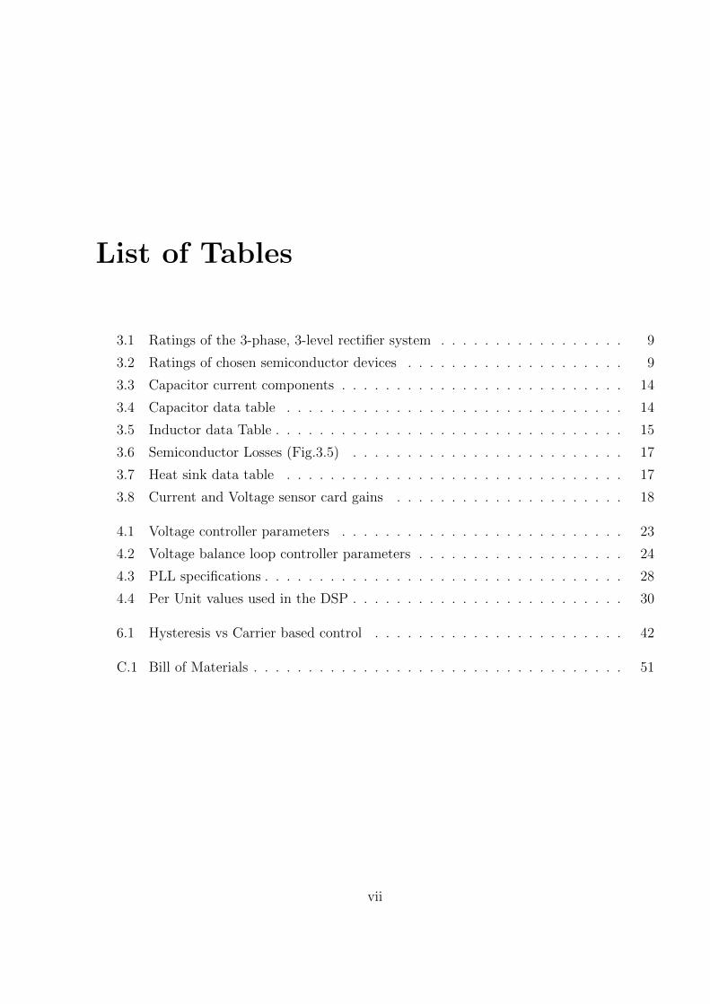
List of Tables
3.1 Ratings of the 3-phase, 3-level rectifier system . . . . . . . . . . . . . . . . . 9
3.2 Ratings of chosen semiconductor devices . . . . . . . . . . . . . . . . . . . . 9
3.3 Capacitor current components . . . . . . . . . . . . . . . . . . . . . . . . . . 14
3.4 Capacitor data table . . . . . . . . . . . . . . . . . . . . . . . . . . . . . . . 14
3.5 Inductor data Table . . . . . . . . . . . . . . . . . . . . . . . . . . . . . . . . 15
3.6 Semiconductor Losses (Fig.3.5) . . . . . . . . . . . . . . . . . . . . . . . . . 17
3.7 Heat sink data table . . . . . . . . . . . . . . . . . . . . . . . . . . . . . . . 17
3.8 Current and Voltage sensor card gains . . . . . . . . . . . . . . . . . . . . . 18
4.1 Voltage controller parameters . . . . . . . . . . . . . . . . . . . . . . . . . . 23
4.2 Voltage balance loop controller parameters . . . . . . . . . . . . . . . . . . . 24
4.3 PLL specifications . . . . . . . . . . . . . . . . . . . . . . . . . . . . . . . . . 28
4.4 Per Unit values used in the DSP . . . . . . . . . . . . . . . . . . . . . . . . . 30
6.1 Hysteresis vs Carrier based control . . . . . . . . . . . . . . . . . . . . . . . 42
C.1 Bill of Materials . . . . . . . . . . . . . . . . . . . . . . . . . . . . . . . . . . 51
vii

List of Figures
1.1 AC-DC Power Converter . . . . . . . . . . . . . . . . . . . . . . . . . . . . . 1
1.2 Input currents of a Diode bridge rectifier with C filter . . . . . . . . . . . . . 2
1.3 Power circuit topology of the project . . . . . . . . . . . . . . . . . . . . . . 2
2.1 Single phase equivalent circuit of the rectifier [2] . . . . . . . . . . . . . . . . 6
2.2 Phasor diagram for UPF operation . . . . . . . . . . . . . . . . . . . . . . . 6
3.1 Power circuit topology of the 3-phase, 3-level rectifier . . . . . . . . . . . . . 8
3.2 Single phase equivalent circuit of Fig. 3.1 . . . . . . . . . . . . . . . . . . . . 9
3.3 Duty ratio variation of the switches Sa, Sb, Sc . . . . . . . . . . . . . . . . . . 12
3.4 Switching functions and expressions for iprms−k and ipavg−k . . . . . . . . . . 13
3.5 Thermal calculations . . . . . . . . . . . . . . . . . . . . . . . . . . . . . . . 17
4.1 Control unit based on Hysteresis controller [2] . . . . . . . . . . . . . . . . . 21
4.2 Voltage control loop . . . . . . . . . . . . . . . . . . . . . . . . . . . . . . . 23
4.3 Bode plot of the open loop transfer function of voltage control loop (Fig. 4.2) 23
4.4 Control diagram for the proposed carrier based control strategy . . . . . . . 25
4.5 Current control loop . . . . . . . . . . . . . . . . . . . . . . . . . . . . . . . 26
4.6 Bode plot of the open loop transfer function of the current loop . . . . . . . 26
4.7 PLL control structure . . . . . . . . . . . . . . . . . . . . . . . . . . . . . . . 27
4.8 Locking feature of the PLL (Experimental result) . . . . . . . . . . . . . . . 28
4.9 θ generation of PLL (Experimental result) . . . . . . . . . . . . . . . . . . . 28
5.1 Input currents Ia [I(L1)], Ib [I(L2)] of the rectifier (Hysteresis based control) 32
5.2 Frequency spectrum of Input current Ia of the rectifier (Hysteresis based control) 32
viii

List of Figures ix
5.3 Input phase voltage Va [V(vr)] and Input current Ia [I(L1)] (Hysteresis based
control) . . . . . . . . . . . . . . . . . . . . . . . . . . . . . . . . . . . . . . 33
5.4 Voltages across the DC bus capacitors Vc1, Vc2 (Hysteresis based control) . . 33
5.5 Input currents Ia [I(L1)], Ib [I(L2)] of the rectifier (Carrier based control) . . 34
5.6 Frequency spectrum of Input current Ia of the rectifier (Carrier based control) 34
5.7 Input phase voltage Va [V(vr)] and Input current Ia [I(L1)] (Carrier based
control) . . . . . . . . . . . . . . . . . . . . . . . . . . . . . . . . . . . . . . 35
5.8 Voltages across the DC bus capacitors Vc1, Vc2 (Carrier based control) . . . . 35
6.1 Input currents Ia [Ch.1, Scale: 0.58A/1V], Ib [Ch.2, Scale: 0.59A/1V] of the
rectifier . . . . . . . . . . . . . . . . . . . . . . . . . . . . . . . . . . . . . . 38
6.2 Input current Ia [Ch.1, Scale: 2A/div] and Input phase voltage Van [Ch.2,
Scale: 50V/div] indicating UPF operation . . . . . . . . . . . . . . . . . . . 38
6.3 Voltages across the DC bus capacitors Vc1 [Ch.1, Scale: 46.2V/1V], Vc2 [Ch.2,
Scale: 44.8V/1V] . . . . . . . . . . . . . . . . . . . . . . . . . . . . . . . . . 39
6.4 Input currents Ia [Ch.1, Scale: 0.58A/1V], Ib [Ch.2, Scale: 0.59A/1V] of the
rectifier . . . . . . . . . . . . . . . . . . . . . . . . . . . . . . . . . . . . . . 39
6.5 Input current Ia [Ch.1, Scale: 2A/div] and Input phase voltage Van [Ch.2,
Scale: 50V/div] indicating UPF operation . . . . . . . . . . . . . . . . . . . 40
6.6 Voltages across the DC bus capacitors Vc1 [Ch.1, Scale: 46.2V/1V], Vc2 [Ch.2,
Scale: 44.8V/1V] . . . . . . . . . . . . . . . . . . . . . . . . . . . . . . . . . 40
6.7 Duty ratio variation da and line current Ia [Ch.2, Scale: 2A/div] . . . . . . . 41
6.8 Input currents Ia [Ch.1, Scale: 0.58A/1V], Ib [Ch.2, Scale: 0.59A/1V] of the
rectifier . . . . . . . . . . . . . . . . . . . . . . . . . . . . . . . . . . . . . . 43
6.9 Input current Ia [Ch.1, Scale: 0.58A/1V] and Input phase voltage Va [Ch.2,
Scale: 38.5V/1V] . . . . . . . . . . . . . . . . . . . . . . . . . . . . . . . . . 43
6.10 Voltages across the DC bus capacitors Vc1 [Ch.1, Scale: 46.2V/1V], Vc2 [Ch.2,
Scale: 44.8V/1V] and Vdc (Vc1 + Vc2) . . . . . . . . . . . . . . . . . . . . . . 44
6.11 Line-line voltage [Scale: 250V/div] (Vra−Vrb) (Fig. 1.3) at the rectifier input
terminals . . . . . . . . . . . . . . . . . . . . . . . . . . . . . . . . . . . . . . 44
6.12 Phase voltage at the rectifier input terminal Vra [Scale: 250V/div] w.r.t to the
neutral point of the AC grid. (Fig. 1.3) . . . . . . . . . . . . . . . . . . . . . 45

x List of Figures
A.1 Power circuit topology of the Vienna rectifier [2] . . . . . . . . . . . . . . . . 48
B.1 Semiconductor loss comparison . . . . . . . . . . . . . . . . . . . . . . . . . 49
C.1 Schematic of the 3-Phase, 3-level rectifier . . . . . . . . . . . . . . . . . . . . 52
D.1 Component positions in bottom layer . . . . . . . . . . . . . . . . . . . . . . 54
D.2 Bottom layer of the PCB . . . . . . . . . . . . . . . . . . . . . . . . . . . . . 55
D.3 Component positions in top layer . . . . . . . . . . . . . . . . . . . . . . . . 56
D.4 Top layer of the PCB . . . . . . . . . . . . . . . . . . . . . . . . . . . . . . . 57
E.1 Circuit for testing of diodes on the PCB . . . . . . . . . . . . . . . . . . . . 58
E.2 Voltage across diode Da2 and input current ia . . . . . . . . . . . . . . . . . 59
E.3 Voltage across diode Da2 and DC bus voltage Vdc . . . . . . . . . . . . . . . 59
E.4 Circuits for testing of mosfets on the PCB . . . . . . . . . . . . . . . . . . . 60
E.5 Gate-source voltage Vgs and Drain-source voltage Vds of the switched mosfet 60
E.6 Voltages across capacitors C1 and C2 when mosfets are not switched . . . . . 61
E.7 Voltages across capacitors C1 and C2 when mosfets are switched . . . . . . . 61
F.1 Front view of the rectifier . . . . . . . . . . . . . . . . . . . . . . . . . . . . 62
F.2 Back view of the rectifier . . . . . . . . . . . . . . . . . . . . . . . . . . . . . 63
F.3 Complete Hardware setup . . . . . . . . . . . . . . . . . . . . . . . . . . . . 63

Nomenclature
Symbols : Definitions
Vdc : DC bus voltage
Vri−M : Rectifier input terminal voltage (i=a,b,c) w.r.t DC bus neutral point M
Sa, Sb, Sc : The three active switches of the rectifier
ω0 : Grid frequency in rad/s
Vm : Peak value of the per-phase input voltage
Im : Peak value of the fundamental component of input current
Ton : ‘ON’ period of the switch within a time period Ts (Ton ≤ Ts)
Ts : Time period of one switching cycle
imavg : Average current injected into DC bus neutral point in a switching cycle
Idc, ipdc : Output DC current flowing through the load
M0 : Modulation index - Ratio of modulating signal peak to carrier wave peak
ipfsw : Switching frequency current ripple in the DC bus
ip150 : 150 Hz current ripple in the DC bus
Fs : Frequency of the carrier wave
δipk−pk : Peak to peak current ripple in line current
δipk−pk−max : Worst case switching frequency current ripple in line current
h : Width of the Hysteresis band
Kpv, Kiv : Gains of PI controller (outer voltage loop)
Kpb, Kib : Gains of PI controller (voltage balance loop)
Kpc : Gain of the proportional controller (current controller)
Vcpk : Peak value of the triangular carrier wave
Ia, Ib, Ic : The three input line currents of the rectifier
xi
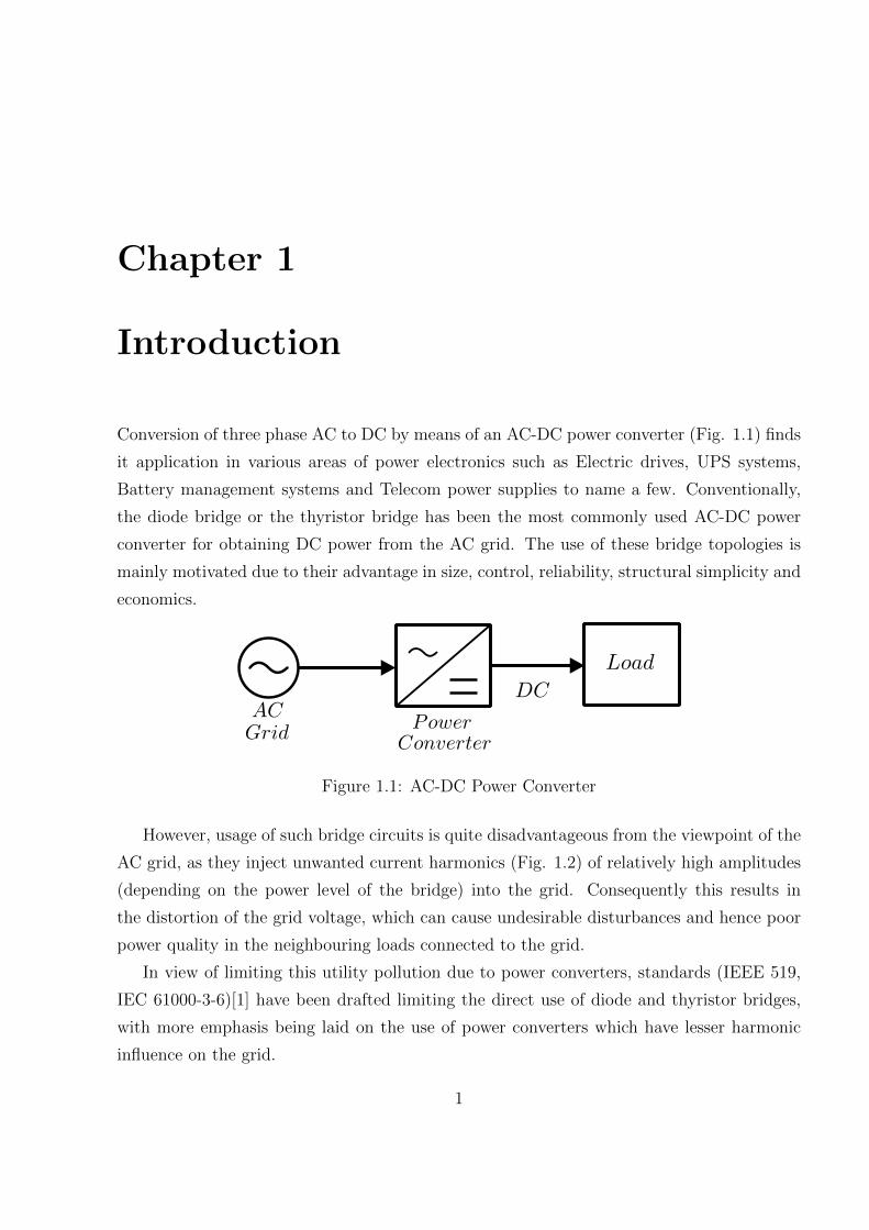
Chapter 1
Introduction
Conversion of three phase AC to DC by means of an AC-DC power converter (Fig. 1.1) finds
it application in various areas of power electronics such as Electric drives, UPS systems,
Battery management systems and Telecom power supplies to name a few. Conventionally,
the diode bridge or the thyristor bridge has been the most commonly used AC-DC power
converter for obtaining DC power from the AC grid. The use of these bridge topologies is
mainly motivated due to their advantage in size, control, reliability, structural simplicity and
economics.
Figure 1.1: AC-DC Power Converter
However, usage of such bridge circuits is quite disadvantageous from the viewpoint of the
AC grid, as they inject unwanted current harmonics (Fig. 1.2) of relatively high amplitudes
(depending on the power level of the bridge) into the grid. Consequently this results in
the distortion of the grid voltage, which can cause undesirable disturbances and hence poor
power quality in the neighbouring loads connected to the grid.
In view of limiting this utility pollution due to power converters, standards (IEEE 519,
IEC 61000-3-6)[1] have been drafted limiting the direct use of diode and thyristor bridges,
with more emphasis being laid on the use of power converters which have lesser harmonic
influence on the grid.
1

2 Chapter 1. Introduction
Figure 1.2: Input currents of a Diode bridge rectifier with C filter
A reduction in current harmonic injection into the grid can be achieved by using effective
control strategies on pulse width modulated (PWM) rectifiers such as the vienna rectifier
[2], [3], [4], force commutated three level boost type rectifier [5] or many other improved power
quality converter topologies that exist in literature. An exhaustive review of such topologies
can be found in [6].
1.1 Project Work
This project deals with the hardware design, development and control of a 3-phase, 3-level
UPF rectifier whose power circuit is shown in Fig. 1.3.
Figure 1.3: Power circuit topology of the project

1.2. Organization of the thesis 3
As part of the project, literature on improved power quality converters [6] was looked
into. Particularly, literature on vienna rectifier and force commutated boost rectifier were
studied. [2] discusses the vienna rectifier topology. [3] presents a space vector based analysis
of the control strategy proposed in [2]. Papers [4] and [7] discuss about the neutral point
current handling capability of the rectifier and development of a semi-conductor module for
each leg of the rectifier. [5] discusses about the force commutated boost rectifier topology
and its control.
The power circuit topology (Fig. 1.3) used in the project is a variant of the vienna
rectifier [2], [3] (Refer Appendix Fig. A.1). The reduced component count in the power
circuit topology compared to the vienna rectifier offers a scope for reduction in the size of
rectifier (reduced PCB size) and eases packaging effort (Refer Appendix B.1). The 3-phase,
3-level rectifier is characterised by its input currents being almost sinusoidal, reduced input
current ripple, reduced filter requirement, high power density, high reliability, controllable
output DC voltage and UPF operation.
A broad overview of the project tasks is as follows:
• Hardware design and development of the power circuit (Fig. 1.3) for the required
specifications (Table 3.1).
• Control of the rectifier
– Rectifier control using Hysteresis based control strategy proposed in [2].
– Proposal of a control strategy based on carrier comparison and its validation on
the hardware setup.
1.2 Organization of the thesis
Chapter 1 provides a brief introduction about the project followed by chapter 2 which dis-
cusses the operating principle of the UPF rectifier used in the project.
Chapter 3 discusses the hardware design in detail. The selection of switches, DC bus
capacitors, filter inductors, heat sinks and the development of main circuit board is discussed.
Chapter 4 includes the details of the control system design and implementation of the
same in digital domain for hysteresis based control strategy as well as the proposed carrier
based control strategy.

4 Chapter 1. Introduction
In chapter 5, simulation results of the hysteresis and carrier based control strategy are
included. The simulations are carried out using LT-Spice [8].
Chapter 6 contains all the experimental results with pertinent waveforms, along with a
comparison between the proposed and existing control strategies. Conclusion and Future
work are discussed in chapter 7.
The schematics of main circuit board, PCB layout and the pictures of the hardware setup
along with test circuits for testing of power circuit PCB are provided in Appendix.

Chapter 2
Operating Principle of the 3-phase,
3-level Rectifier
This chapter discusses the three level characteristic of the rectifier (Fig. 1.3) along with its
basic functionality regarding the control of input current [2]. The analysis has been restricted
to quantities only at fundamental frequency.
2.1 Three level characteristic
The power circuit of the 3-phase, 3-level rectifier is shown in Fig. 1.3. From the power circuit
it can be seen that the rectifier input terminal voltage Vra−M is clamped to the neutral point
of the DC bus (M) when the switch Sa is ‘on’. When Sa is ‘off’, Vra−M can take a value of
±Vdc
2depending on the polarity of the current ia i.e.
Vra−M =
sign(ia)
Vdc
2if Sa = ON
0 if Sa = OFF(2.1)
Thus the pole voltage Vri−M(i=a,b,c) of each leg of the converter can have 3 discrete values
depending on the state of the switch Si(i=a,b,c) and the direction of input current. Accordingly
the system is called a 3-level PWM rectifier.
2.2 Basic functionality
The single phase equivalent circuit of the rectifier (Fig. 1.3) can be represented as shown in
Fig. 2.1 where Vi represents the single phase grid voltage and Vri represents the per-phase
rectifier input voltage.
5

6 Chapter 2. Operating Principle of the 3-phase, 3-level Rectifier
Figure 2.1: Single phase equivalent circuit of the rectifier [2]
Restricting the analysis to quantities at fundamental frequency alone, the rectifier input
voltage can be written as,
Vri = Vi − jω0LIi (2.2)
Where,
Vi = Vmcos(ω0t) (2.3)
The current through the inductor is defined by the voltage difference across it and for
the case of UPF operation, the current can be written as,
Ii = Imcos(ω0t) (2.4)
The control of this current is done by controlling the voltage difference across the inductor
which is given by the difference of the grid voltage Vi and the rectifier input voltage Vri. The
voltage Vri is controlled at the required phase and magnitude by appropriate switching of the
bi-directional switches Si (using a suitable PWM strategy) at high frequencies. The current
ripple at these high switching frequencies is attenuated to a great extent by the line and
filter inductances resulting in the input current mainly containing the fundamental current
component at 50Hz along with switching frequency ripple.
Figure 2.2: Phasor diagram for UPF operation
From the phasor diagram in Fig. 2.2, it can be seen that the magnitude of the rectifier
input voltage Vri is greater than the input grid voltage, illustrating the ‘boost’ nature of the

2.2. Basic functionality 7
rectifier. Thus the DC output voltage that can be obtained from the rectifier can only be
greater than the peak value of the input line-line voltage.
The DC power delivered to load under UPF operation is given by power balance as
(neglecting the system losses),
Pdc = VdcIdc =3
2VmIm (2.5)
The details about the space vector representation of the rectifier and its operating region
can be referred to in [2], [5].
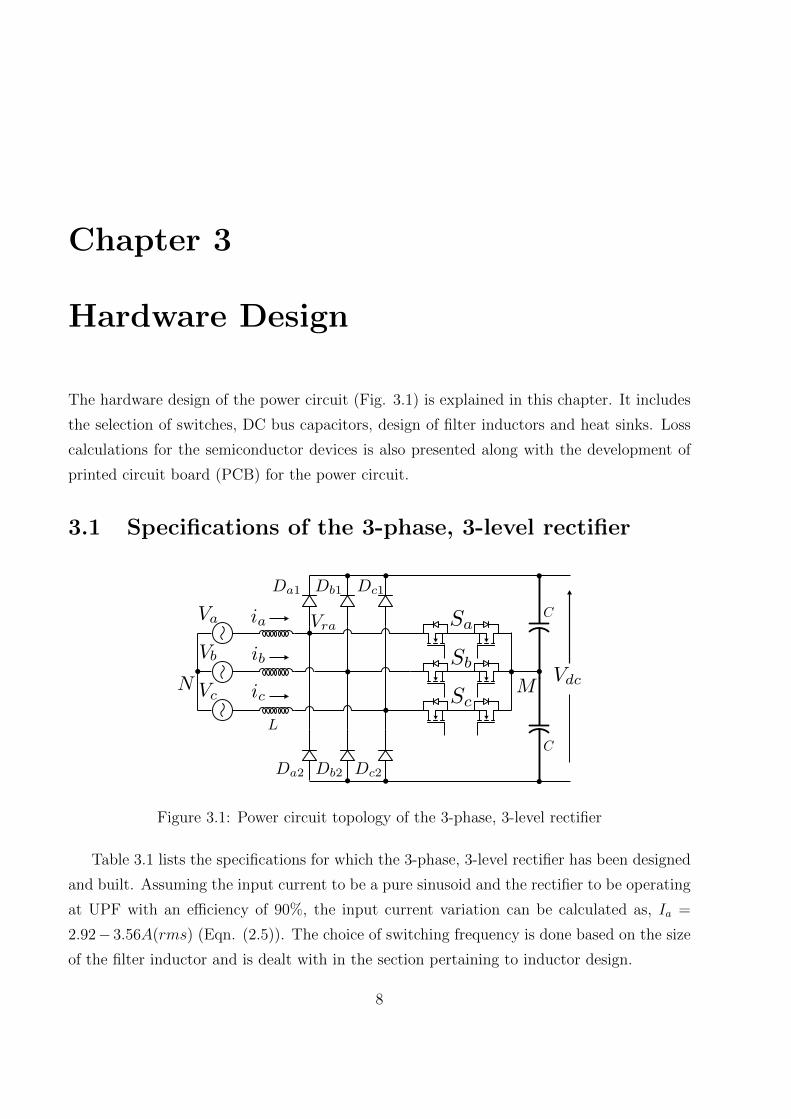
Chapter 3
Hardware Design
The hardware design of the power circuit (Fig. 3.1) is explained in this chapter. It includes
the selection of switches, DC bus capacitors, design of filter inductors and heat sinks. Loss
calculations for the semiconductor devices is also presented along with the development of
printed circuit board (PCB) for the power circuit.
3.1 Specifications of the 3-phase, 3-level rectifier
Figure 3.1: Power circuit topology of the 3-phase, 3-level rectifier
Table 3.1 lists the specifications for which the 3-phase, 3-level rectifier has been designed
and built. Assuming the input current to be a pure sinusoid and the rectifier to be operating
at UPF with an efficiency of 90%, the input current variation can be calculated as, Ia =
2.92− 3.56A(rms) (Eqn. (2.5)). The choice of switching frequency is done based on the size
of the filter inductor and is dealt with in the section pertaining to inductor design.
8

3.2. Device selection 9
Table 3.1: Ratings of the 3-phase, 3-level rectifier system
Quantity Rated value
Output DC power 2kW
Input 3φ AC line-line voltage 360− 440V
Frequency of input voltage 50Hz ± 5%
Output DC voltage, Vdc 750V
Switching frequency, Fs 20kHz
Controller platform TMS320LF2407A
3.2 Device selection
From Fig. 3.2 it can be seen that the diodes Da1, Da2 should have a voltage blocking
capability of 750V , and should be able to conduct a peak current of 5.03A. Similarly the
mosfets T1, T2 should be able conduct a peak current of 5.03A with voltage blocking capability
of 375V . Accordingly, the devices chosen are shown in Table 3.2.
Table 3.2: Ratings of chosen semiconductor devices
Device Avg. forward current Blocking voltage
MUR8100 (Diode-FRED) 12 A 1000 V
IRF840 (Mosfet) 8 A 500 V
Figure 3.2: Single phase equivalent circuit of Fig. 3.1

10 Chapter 3. Hardware Design
3.3 Capacitor Design
The design of capacitors is done for the nominal input line-line voltage (400 V (rms)) and
nominal input current (3.21 A(rms)) rating of the circuit. The circuit is assumed to be
operating at UPF and the input currents are assumed to be sinusoidal in nature,
ia = 4.54cos(ω0t)
ib = 4.54cos(ω0t−2π
3) (3.1)
ic = 4.54cos(ω0t+2π
3)
The switches Sa, Sb, Sc are switched at high frequency employing a PWM technique so
that the voltage Vra (Fig. 3.2) contains the required fundamental frequency component at
50Hz with its remaining frequency components close to the switching frequency.
Assuming that the switches are switched using sine-triangle modulation technique the
duty ratios (Ton/Ts) of the switches Si are given by,
da = 0.5 +M0cos(ω0t)
db = 0.5 +M0cos(ω0t−2π
3) (3.2)
dc = 0.5 +M0cos(ω0t+2π
3)
Where, di(i = a, b, c) is the duty ratio corresponding to the switch Si and M0 is the
modulation index which is the ratio of modulating signal peak to the peak of triangular
carrier signal.
From Fig. 3.2 it can be seen that the average current (imavg) injected into the neutral
point of the DC bus over a switching cycle is given by,
imavg = daia + dbib + dcic (3.3)
From Equations (3.1), (3.2) and (3.3) it can be seen that,
imavg = 6.81M0 (3.4)
It can be inferred from Eqn. (3.4) that a direct application of the sine-triangle modulation
strategy will not work for the rectifier as it results in constant injection of DC current into

3.3. Capacitor Design 11
the neutral point of the capacitors in every switching cycle, leading to an uneven voltage
build up across the individual capacitors of the DC bus and hence an unstable system.
Hence for the sizing of capacitor bank, a change is made in the type of modulation signal
used so that there is no net DC current flow into the neutral point of the capacitors over a
fundamental cycle.
It can be seen from Fig. 3.2 that,
when ia > 0
Sa = on(1) ⇒ Vra−M = 0
Sa = off(0) ⇒ Vra−M = +Vdc/2.(3.5)
and, ia < 0
Sa = on(1) ⇒ Vra−M = 0
Sa = off(0) ⇒ Vra−M = −Vdc/2.(3.6)
Accordingly, the duty ratio variation of the switches Sa, Sb, Sc are selected as (Fig. 3.3),
da = 1−M0|cos(ω0t)|
db = 1−M0|cos(ω0t−2π
3)| (3.7)
dc = 1−M0|cos(ω0t+2π
3)|
Where, di(i = a, b, c) is the duty ratio corresponding to the switch Si and M0 is the
modulation index which is the ratio of modulating signal peak to the peak of carrier signal,
which, for the nominal rectifier specifications is found to be,
M0 =2Va(peak)Vdc
= 0.867 (3.8)
Selection of above duty ratios for the switches results in no net DC current injection into
the neutral point of the DC bus over a fundamental cycle (50Hz).
3.3.1 Capacitor ripple current calculation
For the purpose of capacitor selection it is essential to know the amount of ripple current
flowing through the capacitor [9]. Hence the computation of different frequency components
of the positive DC bus current ip (Fig. 3.2) is essential. Computation of ip by analytical
methods and by simulation indicates that ip mainly consists three components - the dc

12 Chapter 3. Hardware Design
Figure 3.3: Duty ratio variation of the switches Sa, Sb, Sc
current component ipdc, the switching frequency current component ipfsw and the 150Hz
current component ip150. It is assumed that the dc current component flows through the
load and other frequency components of ip entirely flow into the capacitor. Hence knowing
the value of ipfsw and ip150, the capacitor can be appropriately sized.
The DC component of current ipdc is found from the Eqn. (2.5) for output power as,
ipdc = Idc =3
2
VmImVdc
= 2.96A (3.9)
For the purpose of finding the switching frequency current component ipfsw, frequency
components of the current greater than the switching frequency are assumed to be lumped at
the switching frequency. This simplifies the calculation of ipfsw as the current components in
each switching cycle can be split into a DC component and a switching frequency component.
The switching frequency component of current over each switching cycle is then summed over
a cycle of fundamental frequency (50Hz) to obtain ipfsw which is given by,
ipfsw =
√√√√ 1
N
N∑k=1
(i2prms−k − i2pavg−k) (3.10)
Where, N = Fs
50, Fs = Frequency of the carrier wave, iprms−k and ipavg−k are the rms and
average values of ip in the kth switching time period.

3.3. Capacitor Design 13
The expressions for iprms−k and ipavg−k change with θ(= ω0t) over a fundamental cycle
and are shown for a range of 0 ≤ θ ≤ 120o in the Fig. 3.4. Exploiting the symmetry of
the duty ratios (Fig. 3.3) the expressions for iprms−k and ipavg−k found over a period of
0 ≤ θ ≤ 120o can be extended to the entire cycle and the switching frequency component of
the current ipfsw can be computed from Eqn. (3.10).
Figure 3.4: Switching functions and expressions for iprms−k and ipavg−k
Once the DC component of current ipdc and the switching frequency component ipfsw
have been computed, the other frequency component at 150 Hz (ip150) is computed using,
ip150 =√i2prms − i2pdc − i2pfsw (3.11)
Where, iprms is the rms value of ip over a fundamental cycle and is given by,
iprms =
√√√√ 1
N
N∑k=1
i2prms−k (3.12)
14 Chapter 3. Hardware Design
Table 3.3: Capacitor current components
Switching Frequency iprms ipdc ipfsw ip150
10 kHz 3.32 A 2.65 A 1.7 A 1.04 A
20 kHz 3.32 A 2.65 A 1.7 A 1.04 A
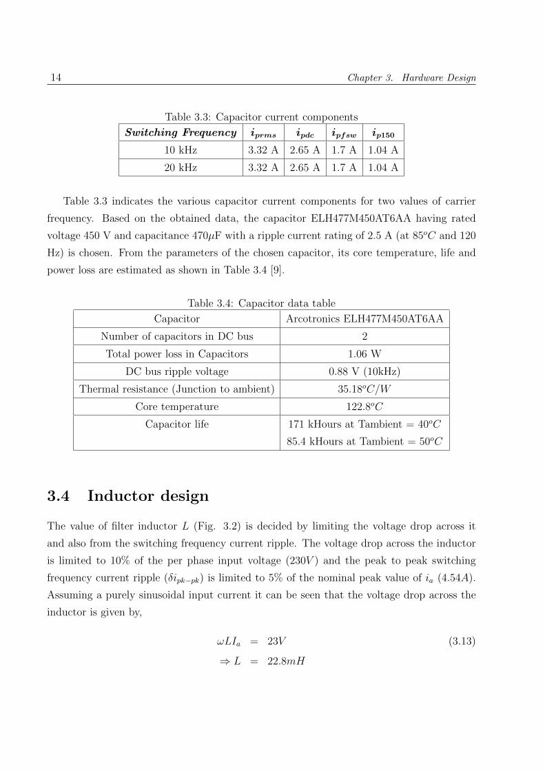
Table 3.3 indicates the various capacitor current components for two values of carrier
frequency. Based on the obtained data, the capacitor ELH477M450AT6AA having rated
voltage 450 V and capacitance 470µF with a ripple current rating of 2.5 A (at 85oC and 120
Hz) is chosen. From the parameters of the chosen capacitor, its core temperature, life and
power loss are estimated as shown in Table 3.4 [9].
Table 3.4: Capacitor data table
Capacitor Arcotronics ELH477M450AT6AA
Number of capacitors in DC bus 2
Total power loss in Capacitors 1.06 W
DC bus ripple voltage 0.88 V (10kHz)
Thermal resistance (Junction to ambient) 35.18oC/W
Core temperature 122.8oC
Capacitor life 171 kHours at Tambient = 40oC
85.4 kHours at Tambient = 50oC
3.4 Inductor design
The value of filter inductor L (Fig. 3.2) is decided by limiting the voltage drop across it
and also from the switching frequency current ripple. The voltage drop across the inductor
is limited to 10% of the per phase input voltage (230V ) and the peak to peak switching
frequency current ripple (δipk−pk) is limited to 5% of the nominal peak value of ia (4.54A).
Assuming a purely sinusoidal input current it can be seen that the voltage drop across the
inductor is given by,
ωLIa = 23V (3.13)
⇒ L = 22.8mH

3.5. Heat sink design 15
Which means that an inductance of value less than 22.8mH has to be chosen to limit the
voltage drop across the inductor to 10% of the input voltage. Further, for the appropriate
choice of the inductance value, an analytical expression is found relating the worst case peak-
peak current ripple δipk−pk−max [10], frequency of the carrier wave and the inductor value as
(the duty ratio variation is assumed as per Fig. 3.3),
δipk−pk−max =87.5
LFs
(3.14)
From the above expression it can be seen that a trade-off has to be done between the
inductor value and the choice of carrier frequency. An increase in inductance value makes the
filter inductor more bulkier and expensive whereas an increase in carrier frequency results
in greater losses and hence a bigger and more expensive heat sink. The trade off is done by
choosing an inductor from the list of available inductors while trying to reduce the carrier
frequency. The chosen values for inductance and carrier frequency are L = 20.26mH and
Fs = 20kHz.
For the chosen values of L(20.26mH) and Fs(20kHz), δipk−pk−max is seen to be less than
5% of the peak value of ia. The data for chosen inductors is shown in Table 3.5
Table 3.5: Inductor data TableInductor Glastronix GX171/45
Current Rating 10 A(rms)
Number of turns 210
Frequency of Operation 50 Hz - 500 Hz
3.5 Heat sink design
3.5.1 Semiconductor power loss calculations
3.5.1.1 Conduction loss
The conduction loss for a diode is given by the expression,
Pdc = (Vd +Rdi)i (3.15)

16 Chapter 3. Hardware Design
Where Vd is the forward voltage drop, Rd is the on-state resistance and i is the cur-
rent flowing through the diode. Similarly the conduction loss in a mosfet is given by the
expression,
Pmc = i2Rds(on) (3.16)
Where i is the current flowing through the mosfet and Rds(on) is the static drain-source
ON resistance.
3.5.1.2 Switching loss
For switching loss computations, turn-on loss for diode is neglected and only turn-off loss is
considered. The turn-off energy loss of the diode is given by,
Ed =QrrVr
2(3.17)
Where, Qrr is the reverse recovery charge and Vr is the voltage blocked by the diode
after turn-off. Similarly, switching energy loss for a mosfet (assuming inductive switching)
is found from the expression,
Em =V i(tr + tf )
2(3.18)
Where, V is the voltage being blocked by the mosfet, i is the current through the mosfet,
tr and tf are the rise and fall times.
From the Equations (3.15)-(3.18) and the duty ratio variation as in Eqn. (3.7), the total
semiconductor power loss over the fundamental cycle is calculated for the selected semicon-
ductor devices (Refer Table 3.2) at nominal ratings of the rectifier. The losses computed are
shown in Table 3.6 for different carrier frequencies.
Heat sink design is done by calculating the required thermal resistance of the heatsink
assuming an ambient temperature Ta = 40oC and the junction temperature of the semicon-
ductors as Tj = 100oC at a switching frequency of 20 kHz.
Thermal resistance Rth =Tj − TaP
(3.19)
Where, P is the power loss in the semiconductor device.
Two diodes of the same leg, e.g. Da1, Da2 (Fig. 3.5) are mounted on a single heat sink
and the two mosfet modules of the same leg are mounted on a single/separate heat sink,
resulting in the use of 6 heat sinks for the rectifier and eliminating the requirement of fan
for cooling. Details of the heat sinks selected are shown in Table 3.7.
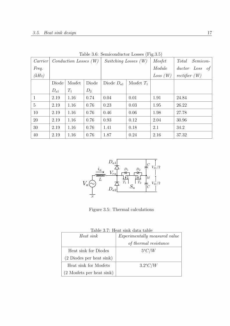
3.5. Heat sink design 17
Table 3.6: Semiconductor Losses (Fig.3.5)
Carrier
Freq.
(kHz)
Conduction Losses (W) Switching Losses (W) Mosfet
Module
Loss (W)
Total Semicon-
ductor Loss of
rectifier (W)
Diode
Da1
Mosfet
T1
Diode
D2
Diode Da1 Mosfet T1
1 2.19 1.16 0.74 0.04 0.01 1.91 24.84
5 2.19 1.16 0.76 0.23 0.03 1.95 26.22
10 2.19 1.16 0.76 0.46 0.06 1.98 27.78
20 2.19 1.16 0.76 0.93 0.12 2.04 30.96
30 2.19 1.16 0.76 1.41 0.18 2.1 34.2
40 2.19 1.16 0.76 1.87 0.24 2.16 37.32
Figure 3.5: Thermal calculations
Table 3.7: Heat sink data tableHeat sink Experimentally measured value
of thermal resistance
Heat sink for Diodes 5oC/W
(2 Diodes per heat sink)
Heat sink for Mosfets 3.2oC/W
(2 Mosfets per heat sink)

18 Chapter 3. Hardware Design
3.6 Auxiliary Hardware
Auxiliary hardware includes isolated gate drive cards for the switches, voltage sensor cards
current sensor card, PD (protection and delay) card and annunciation card [11]. All the
auxiliary hardware systems have been tested according to the procedures in [11]. Since the
rectifier (Fig. 3.1) only requires 3 PWM signals for its 3 bi-directional switches (Mosfet
pairs), the complementary PWM signals from the PD card have not been used. Also, the
dead time logic of the PD card has not been used as the rectifier switches do not have the
requirement of dead time.
The gains of current and voltage sensor cards used as a part of auxiliary hardware is shown
in Table 3.8. The two current sensors have been used to measure two input currents (Ia and
Ib). Among the voltage sensors, voltage sensors 3,4,5 have been used for the measurement of
input AC voltages and the other two voltage sensors (1,2) have been used for measurement
of DC bus voltage.
Table 3.8: Current and Voltage sensor card gains
Current sensor Gain (Vout
Iin) Voltage sensor Gain (Vout
Vin)
Current sensor 1 0.575 V/A Voltage sensor 1 21.66 mV/V
Current sensor 2 0.566 V/A Voltage sensor 2 22.3 mV/V
Voltage sensor 3 26 mV/V
Voltage sensor 4 26.76 mV/V
Voltage sensor 5 26.7 mV/V
3.7 Power Circuit PCB development
The power circuit of the 3-phase, 3-level rectifier (Fig. 3.1) is developed on a PCB and the
salient features of the PCB layout design are indicated below,
• Two layer PCB.
• Component mounting is provided on both sides of the PCB to reduce the size of the
rectifier.

3.7. Power Circuit PCB development 19
• Track widths, clearances and copper foil thickness (70µm) has been chosen based on
the IPC-2221 standard [12]. (Current density ≈ 12.5A/mm2)
• Vias have been used for equalization of current distribution in the PCB tracks.
• Thermal reliefs have been used on all points connected to the copper pour areas.
• Zener card [11] for the switches has been included in the PCB.
• Physical dimensions of the PCB : 26.2 cm X 16.5 cm.
• Physical dimensions of the Rectifier power circuit : 26.2 cm X 17 cm X 7.5 cm.
• Power density (Output power per unit volume) ≈ 600W/dm3
The circuit schematic and PCB layout diagrams are given in the appendix.

Chapter 4
Control of the Rectifier
This chapter discusses the control of the rectifier based on hysteresis controller along with
proposal of a control strategy based on carrier comparision method. The design of con-
trollers, phase locked loop (PLL) is discussed along with digital controller specifications and
implementation of the the controllers in digital domain.
4.1 Hysteresis based control of the rectifier [2]
The Hysteresis based control strategy proposed for the vienna rectifier [2], [3] is also imple-
mented for the 3-phase, 3-level rectifier. A brief discussion of the control strategy is given
below.
The control of the rectifier input voltage Vri (Fig. 1.3) and the wave-shaping of input
currents can be performed by the use of individual hysteresis controllers for each of the
phase currents. The generation of current reference for UPF case is done by multiplying the
output of the voltage controller with sine waves of unit amplitude and in phase with the
input voltages as (Fig. 4.1),
I∗i = INVi(i=a,b,c)
Vm(4.1)
While generating the control signals si for the mosfets, the dependency of the rectifier
input voltage on the sign of the input current (Equation (2.1)) also has to be taken into
consideration by an inversion as,
si =
s′i if i∗i ≥ 0
NOT s′i if i∗i < 0(4.2)
20

4.1. Hysteresis based control of the rectifier [2] 21
Figure 4.1: Control unit based on Hysteresis controller [2]
s′i =
0 if ii ≥ i∗i + h
1 if ii < i∗i − h(4.3)
Where, h is the width of the hysteresis band.
As mentioned earlier in Chapter 2, the control of mains current is done by control of the
voltage difference across the inductor L. The control error of the current control loop i.e.
the maximum current ripple error in the phase currents is limited to the twice the value of
the hysteresis band (2h).
Along with the control of mains current, it is also essential to balance the DC bus voltage
across the capacitors C1 and C2 (Fig. 1.3). The imbalance in the DC bus voltages can be
caused by the loading of DC bus neutral point M by a DC current or by low frequency AC
current and it can be characterised by the difference in voltage across the capacitors as,
vM =1
2(Vc1 − Vc2) (4.4)
The balance of these partial voltages (Vc1, Vc2) across C1 and C2 can be achieved by ad-
dition of a zero sequence component to the current references by a voltage balance controller
F (s) as shown in Fig. 4.1,

22 Chapter 4. Control of the Rectifier
i∗a = I∗a + i0
i∗b = I∗b + i0 (4.5)
i∗c = I∗c + i0
The addition of a zero sequence component i0 has no direct influence on the mains current
shape (as the mains current amplitude and shape is set by current controller and the output
voltage controller) but influences the duration of the switching states and hence the current
iM (Fig. 3.2) flowing into the neutral point of the DC bus [3].
4.2 Design of controller parameters for Hysteresis based
control strategy
The outer voltage controller G(s) and the voltage balance controller F (s) (Fig. 4.1) are both
realized as PI controllers and are designed on the basis of bode plots for the system.
G(s) = Kpv +Kiv
s(4.6)
F (s) = Kpb +Kib
s(4.7)
The system can be modelled as shown in Fig. 4.2 for determining the voltage controller
parameters (here the current controller is modelled as having unity gain with a bandwidth
equal to half the sampling frequency (= 20kHz)). The bandwidth of the voltage loop should
be much less than that of the current controller as the voltage loop has to be much slower
than the current controller loop. Hence the bandwidth of the voltage loop is chosen to be
30 times lesser than the bandwidth of the current controller. Accordingly, the zero of the
voltage controller is placed at ω = 1.22rad/s and the parameters for the voltage controller
are shown in Table 4.1. The bode plot of the open loop transfer function (OLTF) of the
voltage control loop with the controller is shown in Fig 4.3.
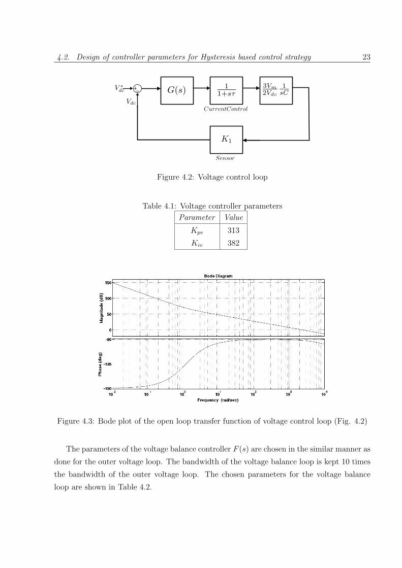
4.2. Design of controller parameters for Hysteresis based control strategy 23
Figure 4.2: Voltage control loop
Table 4.1: Voltage controller parameters
Parameter Value
Kpv 313
Kiv 382
Figure 4.3: Bode plot of the open loop transfer function of voltage control loop (Fig. 4.2)
The parameters of the voltage balance controller F (s) are chosen in the similar manner as
done for the outer voltage loop. The bandwidth of the voltage balance loop is kept 10 times
the bandwidth of the outer voltage loop. The chosen parameters for the voltage balance
loop are shown in Table 4.2.

24 Chapter 4. Control of the Rectifier
Table 4.2: Voltage balance loop controller parameters
Parameter Value
Kpb 62.6
Kib 764
4.3 Proposed carrier based control
Though hysteresis based carrier control is advantageous due to its simplicity, and good
dynamics it has the following disadvantages -
• The rectifier switching frequency to a large extent depends on the load parameters and
the hysteresis band.
• Switching frequency is not constant, which can produce unpleasant acoustic noise.
• The current error is not strictly limited. Double the current error magnitude permitted
by the hysteresis controller can occur at maximum value of current.
Hence a carrier based control approach is proposed in which a modulating signal is
compared with a triangular carrier of fixed frequency. This method eliminates the drawbacks
of varying switching frequency of the hysteresis controller as the carrier based approach
results in the input currents of the rectifier with well defined harmonic contents.
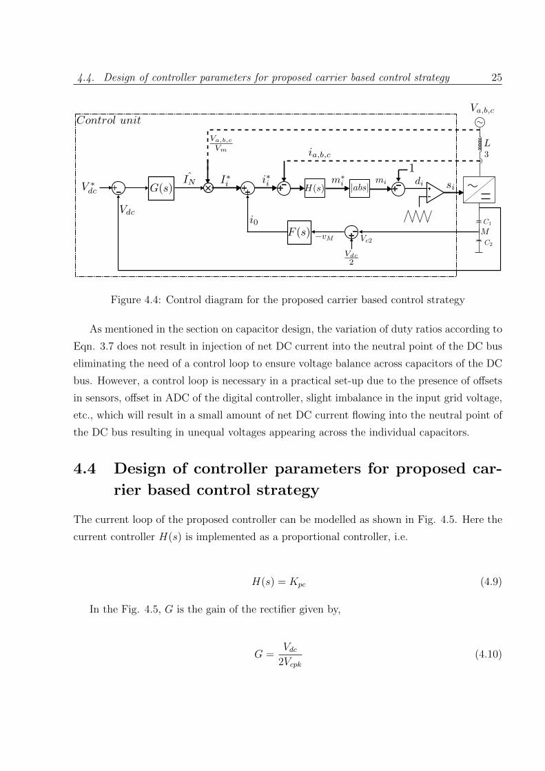
The control diagram for the carrier based control is shown in Fig. 4.4.
The general structure of the control loop (Fig. 4.4) is similar to the loop structure of the
hysteresis based controller (Fig. 4.1). The current control loop of the proposed controller
consists of a current controller H(s), whose output is sent to an absolute value finder (|abs|)followed by the generation of di which is compared with a triangular carrier (similar to
sine-triangle comparison) to generate the switching signals si for the mosfets.
di = 1− |m∗i | (4.8)
The essential idea is to generate modulation signals of the type shown in Fig. 3.3 from
the error between the reference current and the feedback current. The generated modulation
signal is then compared with the triangular carrier to generate the switching pulses for the
mosfets.
4.4. Design of controller parameters for proposed carrier based control strategy 25
Figure 4.4: Control diagram for the proposed carrier based control strategy
As mentioned in the section on capacitor design, the variation of duty ratios according to
Eqn. 3.7 does not result in injection of net DC current into the neutral point of the DC bus
eliminating the need of a control loop to ensure voltage balance across capacitors of the DC
bus. However, a control loop is necessary in a practical set-up due to the presence of offsets
in sensors, offset in ADC of the digital controller, slight imbalance in the input grid voltage,
etc., which will result in a small amount of net DC current flowing into the neutral point of
the DC bus resulting in unequal voltages appearing across the individual capacitors.
4.4 Design of controller parameters for proposed car-
rier based control strategy
The current loop of the proposed controller can be modelled as shown in Fig. 4.5. Here the
current controller H(s) is implemented as a proportional controller, i.e.
H(s) = Kpc (4.9)
In the Fig. 4.5, G is the gain of the rectifier given by,
G =Vdc
2Vcpk(4.10)
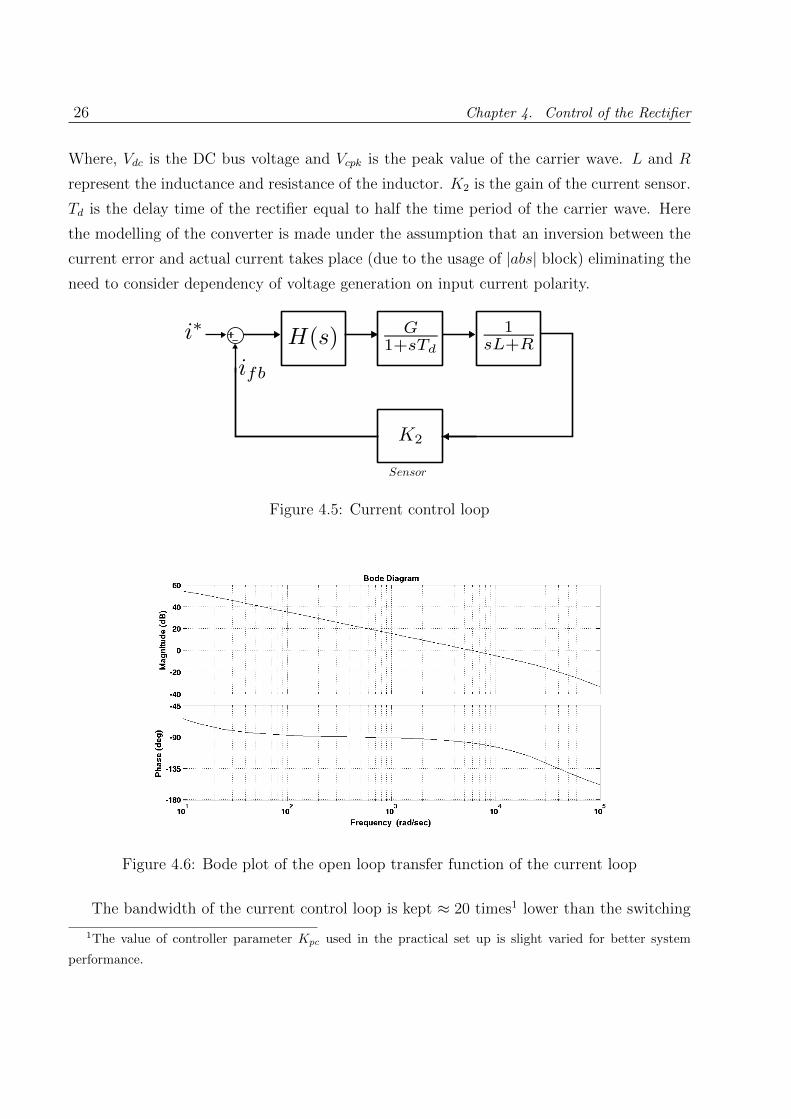
26 Chapter 4. Control of the Rectifier
Where, Vdc is the DC bus voltage and Vcpk is the peak value of the carrier wave. L and R
represent the inductance and resistance of the inductor. K2 is the gain of the current sensor.
Td is the delay time of the rectifier equal to half the time period of the carrier wave. Here
the modelling of the converter is made under the assumption that an inversion between the
current error and actual current takes place (due to the usage of |abs| block) eliminating the
need to consider dependency of voltage generation on input current polarity.
Figure 4.5: Current control loop
Figure 4.6: Bode plot of the open loop transfer function of the current loop
The bandwidth of the current control loop is kept ≈ 20 times1 lower than the switching
1The value of controller parameter Kpc used in the practical set up is slight varied for better system
performance.

4.5. Phase locked loop 27
frequency (20kHz) accordingly, the value of Kpc is selected as 0.5. The bode plot of the open
loop transfer function of the current control loop is shown in Fig 4.6.
The controllers for outer voltage loop and the voltage balance loop have been realized as
PI controllers and their design is done in the same manner as in the case of the hysteresis
based control strategy.
4.5 Phase locked loop
Generation of current references in both hysteresis and carrier based control strategy re-
quires multiplication of DC voltage controller output by unit amplitude sine waves which
are synchronised with the input voltages of the grid. The generation of these sine waves can
be done by using voltage sensors as shown in Figures 4.1 and 4.4. But the usage of voltage
sensors in generation of unit sine waves can result in the transfer of grid disturbances into
the control circuit resulting in increased current harmonic injection into the grid. Hence a
phase locked loop (PLL) is used to generate sine waves of unit amplitude, synchronised with
the grid and free of any grid disturbances.
The structure of the implemented PLL is shown in Fig. 4.7. The implementation of PLL
is done based on the dq transform method discussed in [13].
Figure 4.7: PLL control structure
The design specifications of PLL is shown in Table 4.3. The locking feature of PLL is
shown in Fig. 4.8 and the generation of θ (Fig. 4.7) is shown in Fig. 4.9.

28 Chapter 4. Control of the Rectifier
Table 4.3: PLL specifications
Parameter Value
Kp 0.84
Ki 2098
Settling time ≈ 60ms
Figure 4.8: Locking feature of the PLL (Experimental result)
Figure 4.9: θ generation of PLL (Experimental result)

4.6. Digital implementation of control blocks 29
4.6 Digital implementation of control blocks
The digital controller used in this project is texas instruments based DSP TMS320LF2407A
[16] which has an internal clock rate of 40 MHz. It is programmed using assembly level
language. The controller board has on-board ADCs, DACs and PWM generation units. The
controller board is used to obtain the voltage and current signals through the ADC and
output PWM signals to the gate-drive cards which are used to drive the active devices of
the rectifier.
In this section the implementation PI controller in the digital domain is discussed.
4.6.1 PI controller implementation
The equation for PI controller in continuous time domain is
y(t) = kpe(t) + ki
∫ t
0
e(t)dt (4.11)
Discretization of Eqn. (4.11) is done as follows,
Let the discretized proportional part be yp(k). So,
yp(k) = kpe(k) (4.12)
Similarly let the integral portion be yi(k). It can be shown from Euler’s backward rect-
angle rule that
yi(k) = yi(k − 1) + kiTse(k) (4.13)
Where, Ts is the sampling period.
The final discretized output would be,
y(k) = yp(k) + yi(k) (4.14)
4.6.2 Per-unit Values
All the control blocks are implemented in 16-bit digital arithmetic. The per-unit values and
the equivalent hex code are listed in Table 4.4.

30 Chapter 4. Control of the Rectifier
Table 4.4: Per Unit values used in the DSPpu value Hexadecimal representation
2pu 7FFFh
1pu 3FFFh
0 0000h
-1pu C000h
-2pu 8000h

Chapter 5
Simulation Results
In this chapter simulation results for hysteresis based control of rectifier [2] as well as the
proposed carrier based control are presented. The results indicate a well defined harmonic
spectrum of input currents and a significant reduction in the total harmonic distortion (THD)
of input current for carrier based control over the hysteresis based control strategy. The
simulations are performed using LTspice [8].
5.1 Parameters used in Simulation
Simulation is performed at the rated values of rectifier specifications (Output power = 2kW,
Vdc = 750V) for both the control strategies. The designed controller gains are chosen for
the simulation. The hysteresis band is set as h = ±0.075A. The results are shown for UPF
operation of the rectifier.
5.2 Results for Hysteresis based control strategy
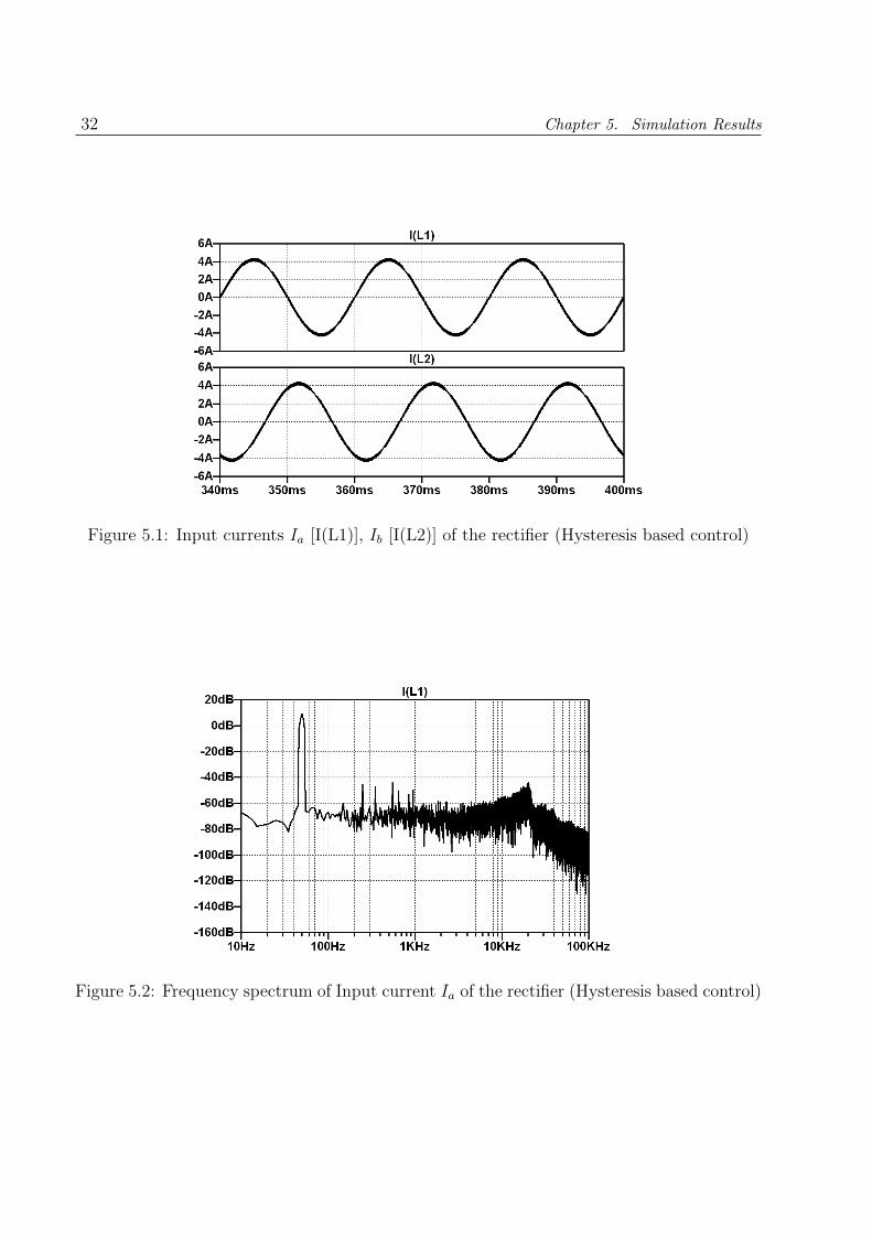
The input line currents of the rectifier are shown in Fig. 5.1.
As seen from the frequency spectrum of Fig. 5.2, the spectrum does not have a dominant
component of switching frequency but rather a band of frequencies indicating the variable
switching frequency characteristic of hysteresis control.
Fig. 5.3 shows the UPF operation of the rectifier and Fig. 5.4 shows the balance of
voltage across the DC bus capacitors.
From the simulation results of Hysteresis based control it is found that the input current
THD is 2.6%.
31
32 Chapter 5. Simulation Results
Figure 5.1: Input currents Ia [I(L1)], Ib [I(L2)] of the rectifier (Hysteresis based control)
Figure 5.2: Frequency spectrum of Input current Ia of the rectifier (Hysteresis based control)

5.2. Results for Hysteresis based control strategy 33
Figure 5.3: Input phase voltage Va [V(vr)] and Input current Ia [I(L1)] (Hysteresis based
control)
Figure 5.4: Voltages across the DC bus capacitors Vc1, Vc2 (Hysteresis based control)

34 Chapter 5. Simulation Results
5.3 Results for carrier based control strategy
Figure 5.5: Input currents Ia [I(L1)], Ib [I(L2)] of the rectifier (Carrier based control)
Figure 5.6: Frequency spectrum of Input current Ia of the rectifier (Carrier based control)
From the frequency spectrum of Fig. 5.6 it can be seen that the spectrum has domi-
nant harmonics at the carrier frequency (20kHz) and its multiples unlike its hysteresis based
control counterpart (Fig. 5.2). It can also be seen that the amplitude of frequency com-
ponents below 20kHz for carrier based control are significantly lesser than their hysteresis
based control counterparts.

5.3. Results for carrier based control strategy 35
Figure 5.7: Input phase voltage Va [V(vr)] and Input current Ia [I(L1)] (Carrier based control)
Figure 5.8: Voltages across the DC bus capacitors Vc1, Vc2 (Carrier based control)
Fig. 5.7 shows the UPF operation of the rectifier with carrier based control strategy.
From Fig. 5.8 a 150Hz component of ripple can be observed in the partial voltages Vc1, Vc2,
which is due to the 150Hz current ripple flowing into the capacitor bank as explained in the
section on capacitor design.
From the simulation results for carrier based control it is found that the input current
THD is 2% which is ≈ 23% less than the input current THD of hysteresis based control
strategy (2.6%) at an average switching frequency of 20kHz. The simulation results indicate

36 Chapter 5. Simulation Results
that the proposed carrier based control strategy has a well defined harmonic spectrum (at
switching frequency and its multiples) and results in a substantial reduction of harmonic
current injection into the grid when compared to the hysteresis based control strategy.

Chapter 6
Experimental Results
This chapter presents the experimental results obtained by running the hardware setup of
the 3-phase, 3-level rectifier. Results for both hysteresis based control and carrier based
control strategy are presented along with a comparison between the two strategies. Results
are presented at two different DC bus voltage levels i.e. 400V and 750V.
6.1 Operation of the rectifier at reduced voltage level
Presented below are the experimental results that have been obtained for both carrier based
and hysteresis based control strategies for a reduced DC bus voltage of 400V, input line-line
voltages of 210 V(rms) and a power level of ≈ 450W . The carrier frequency used in carrier
based control is 10kHz and in the hysteresis based control a sampling frequency of 20kHz is
used with a hysteresis band h = ±0.3A. The results presented are for UPF operation of the
rectifier. The efficiency of the entire hardware setup is found to be ≈ 90% for both control
strategies.
6.1.1 Hysteresis based control strategy
Fig. 6.1 shows the input currents of the rectifier. The maximum peak-peak current ripple is
found to be ≈ 1A.
Fig. 6.2 shows the UPF operation of the rectifier and Fig. 6.3 shows the balance of
voltages across the DC bus capacitors.
37

38 Chapter 6. Experimental Results
Figure 6.1: Input currents Ia [Ch.1, Scale: 0.58A/1V], Ib [Ch.2, Scale: 0.59A/1V] of the
rectifier
Figure 6.2: Input current Ia [Ch.1, Scale: 2A/div] and Input phase voltage Van [Ch.2, Scale:
50V/div] indicating UPF operation

6.1. Operation of the rectifier at reduced voltage level 39
Figure 6.3: Voltages across the DC bus capacitors Vc1 [Ch.1, Scale: 46.2V/1V], Vc2 [Ch.2,
Scale: 44.8V/1V]
6.1.2 Carrier based control strategy
Figure 6.4: Input currents Ia [Ch.1, Scale: 0.58A/1V], Ib [Ch.2, Scale: 0.59A/1V] of the
rectifier
Fig. 6.1 shows the input currents of the rectifier for carrier based control. The maximum
peak-peak current ripple is ≈ 0.4A.
Fig. 6.5 shows the UPF operation of the carrier based based control strategy.
Fig. 6.7 shows the duty ratio da variation , and the corresponding line current Ia of the
rectifier (Refer section 4.3).

40 Chapter 6. Experimental Results
Figure 6.5: Input current Ia [Ch.1, Scale: 2A/div] and Input phase voltage Van [Ch.2, Scale:
50V/div] indicating UPF operation
Figure 6.6: Voltages across the DC bus capacitors Vc1 [Ch.1, Scale: 46.2V/1V], Vc2 [Ch.2,
Scale: 44.8V/1V]

6.2. Comparision between the hysteresis based and carrier based control strategies 41
Figure 6.7: Duty ratio variation da and line current Ia [Ch.2, Scale: 2A/div]
6.2 Comparision between the hysteresis based and car-
rier based control strategies
It can be seen from Table 6.1 that the carrier based control strategy results in a significant
reduction (23%) in the input current THD compared to the hysteresis control strategy at
an average switching frequency of 20kHz. Thus a significant reduction in the size of filter
inductor can be achieved using carrier based control over hysteresis based control.
It is also observed that the carrier based control strategy has a well defined harmonic
current spectrum compared to the hysteresis based control strategy, which helps in better
design of magnetics, passive components and a better estimate of semi-conductor losses of
the rectifier. Due to the well behaved harmonic spectrum of the carrier based control it
is also possible to achieve greater reduction in input current THD by using higher order
filters at the input of the rectifier which may not be possible in the case of hysteresis control
strategy.
Also, it was observed during the hardware implementation of the control strategies on
the DSP, that, the hysteresis based control strategy requires a much higher sampling fre-
quency for achieving higher switching frequencies (and hence lesser current ripple). From the
experimental results of hysteresis based control strategy it was observed that the maximum
switching frequency was around 2.5kHz for a sampling frequency of 20kHz. In contrast it
was noted that the switching frequency of the carrier based control strategy was equal to its
sampling frequency.
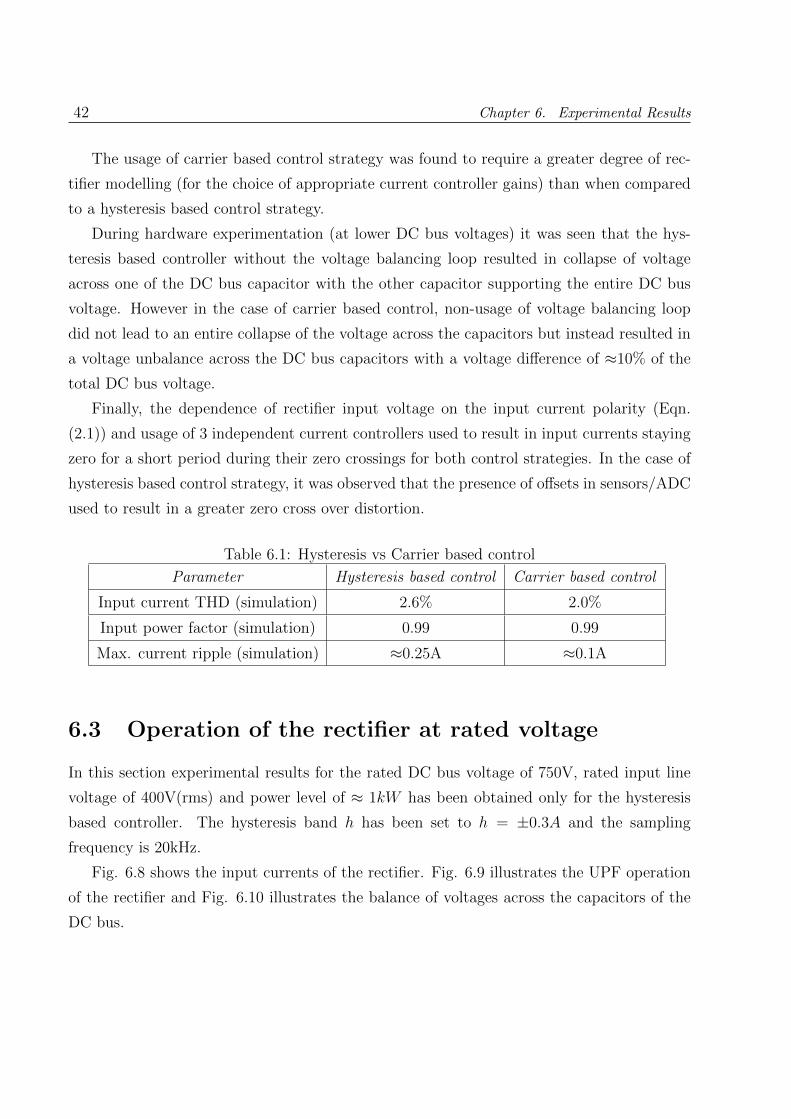
42 Chapter 6. Experimental Results
The usage of carrier based control strategy was found to require a greater degree of rec-
tifier modelling (for the choice of appropriate current controller gains) than when compared
to a hysteresis based control strategy.
During hardware experimentation (at lower DC bus voltages) it was seen that the hys-
teresis based controller without the voltage balancing loop resulted in collapse of voltage
across one of the DC bus capacitor with the other capacitor supporting the entire DC bus
voltage. However in the case of carrier based control, non-usage of voltage balancing loop
did not lead to an entire collapse of the voltage across the capacitors but instead resulted in
a voltage unbalance across the DC bus capacitors with a voltage difference of ≈10% of the
total DC bus voltage.
Finally, the dependence of rectifier input voltage on the input current polarity (Eqn.
(2.1)) and usage of 3 independent current controllers used to result in input currents staying
zero for a short period during their zero crossings for both control strategies. In the case of
hysteresis based control strategy, it was observed that the presence of offsets in sensors/ADC
used to result in a greater zero cross over distortion.
Table 6.1: Hysteresis vs Carrier based control
Parameter Hysteresis based control Carrier based control
Input current THD (simulation) 2.6% 2.0%
Input power factor (simulation) 0.99 0.99
Max. current ripple (simulation) ≈0.25A ≈0.1A
6.3 Operation of the rectifier at rated voltage
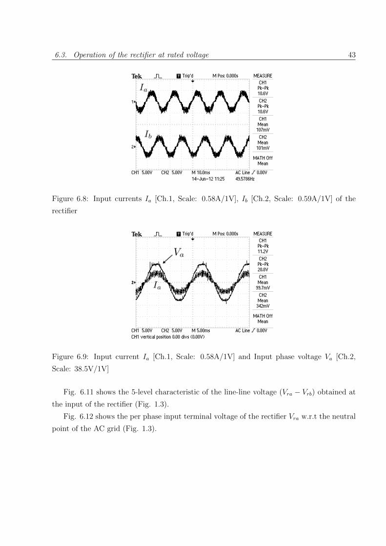
In this section experimental results for the rated DC bus voltage of 750V, rated input line
voltage of 400V(rms) and power level of ≈ 1kW has been obtained only for the hysteresis
based controller. The hysteresis band h has been set to h = ±0.3A and the sampling
frequency is 20kHz.
Fig. 6.8 shows the input currents of the rectifier. Fig. 6.9 illustrates the UPF operation
of the rectifier and Fig. 6.10 illustrates the balance of voltages across the capacitors of the
DC bus.
6.3. Operation of the rectifier at rated voltage 43
Figure 6.8: Input currents Ia [Ch.1, Scale: 0.58A/1V], Ib [Ch.2, Scale: 0.59A/1V] of the
rectifier
Figure 6.9: Input current Ia [Ch.1, Scale: 0.58A/1V] and Input phase voltage Va [Ch.2,
Scale: 38.5V/1V]
Fig. 6.11 shows the 5-level characteristic of the line-line voltage (Vra − Vrb) obtained at
the input of the rectifier (Fig. 1.3).
Fig. 6.12 shows the per phase input terminal voltage of the rectifier Vra w.r.t the neutral
point of the AC grid (Fig. 1.3).
44 Chapter 6. Experimental Results
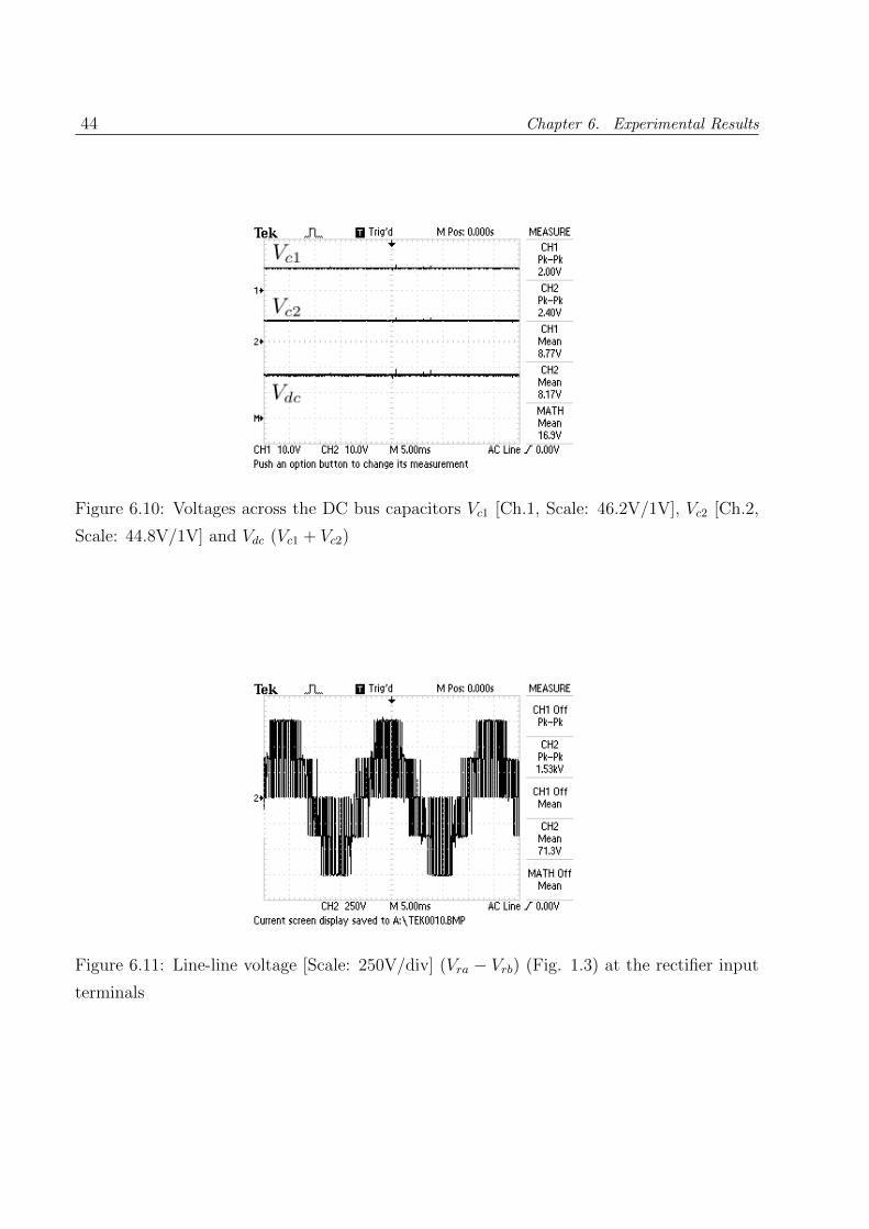
Figure 6.10: Voltages across the DC bus capacitors Vc1 [Ch.1, Scale: 46.2V/1V], Vc2 [Ch.2,
Scale: 44.8V/1V] and Vdc (Vc1 + Vc2)
Figure 6.11: Line-line voltage [Scale: 250V/div] (Vra − Vrb) (Fig. 1.3) at the rectifier input
terminals

6.3. Operation of the rectifier at rated voltage 45
Figure 6.12: Phase voltage at the rectifier input terminal Vra [Scale: 250V/div] w.r.t to the
neutral point of the AC grid. (Fig. 1.3)

Chapter 7
Conclusions
The project was aimed at design and development of hardware for 3-phase, 3-level UPF
rectifier topology along with proposal of a control strategy based on carrier comparison.
Accordingly, the 3-phase, 3-level rectifier has been designed for the required specifications
and the necessary hardware has been developed, assembled and tested. The hardware setup
of the project consists of:
• The power circuit PCB of the 3-phase, 3-level UPF rectifier.
• Gate drive cards, Sensor cards, Protection and delay card, Annunciation card.
• DSP based controller platform.
The control of hardware has been implemented using a texas instruments based DSP
TMS320LF2407A platform. Closed loop control of the rectifier has been executed for both
control strategies i.e. the existing hysteresis based control strategy and the proposed carrier
based control strategy. Phase locked loop (PLL) has also been implemented for generation
of unit sine waves in synchronization with the fundamental frequency of the grid voltages.
It has been observed from semiconductor loss calculations, that the 3-phase, 3-level UPF
rectifier (a variant of vienna rectifier) offers a greater scope for reduction in the size of
rectifier along with reduced packaging effort in contrast to the originally proposed vienna
rectifier [2].
The simulation and experimental results indicate that the carrier based control strategy
(formulated by altering the modulation signals used for sine-triangle comparison), has been
found to result in a well defined harmonic spectrum for input line currents and lesser current
ripple compared to the control of rectifier using hysteresis based control strategy.
46

47
Distortions in the input line currents near their zero crossings were observed during the
hardware implementation of hysteresis based control of the rectifier. Sensor and ADC offsets
were identified as the main reason for such distortions and the problem was solved by nulling
the sensor offsets and by providing software compensation for the ADC offsets in the DSP.
In implementation of carrier based control of the rectifier the above issue was resolved by
inclusion (twisting) of a ground wire with wires carrying current sensor outputs and also by
addition of a small delay angle in the PLL outputs to generate slightly phase shifted current
reference signals.
As part of future work, the rectifier can be run at the rated DC bus voltage (750V) using
carrier based control strategy. A greater detail in the modelling of the rectifier would be
helpful for the design of effective controllers based on carrier based control. The possibility
of using a PR controller in the current loop for better controller performance can be looked
into. An analysis of the proposed carrier based control can be done in the space vector
domain to see if any improvements can be made to the control strategy. Carrier based
control strategies suggested in [14] and [15] can be implemented and comparisons between
the different carrier based control strategies can be done. The EMI issues with the hardware
setup can be studied and the setup can be made compliant with the EMI standards.
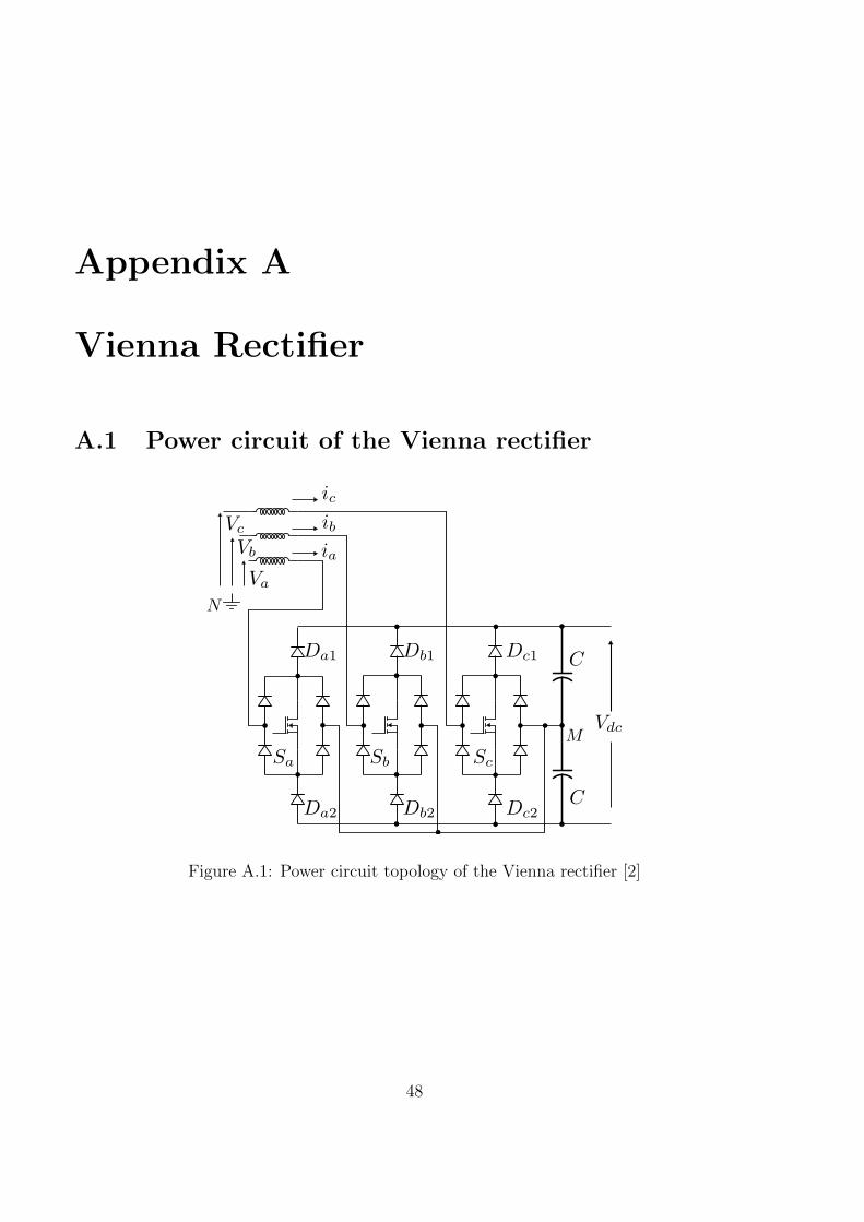
Appendix A
Vienna Rectifier
A.1 Power circuit of the Vienna rectifier
Figure A.1: Power circuit topology of the Vienna rectifier [2]
48

Appendix B
Semiconductor loss comparison
A comparison between the semiconductor losses of the vienna rectifier and the 3-phase,
3-level rectifier is done here. For the comparison of losses the fast recovery diode and
mosfet chosen are DSEP15-06A (IXYS-600V, 15A), IRF840 for the vienna rectifier and
DSEP12-12A (IXYS-1200V, 15A), IRF840 for the 3-phase, 3-level rectifier. The losses
for the both rectifier circuits have been computed in the same manner as discussed in the
section on heat sink design. Fig. B.1 shows the variation of total semiconductor loss of the
power circuits with carrier frequency.
Figure B.1: Semiconductor loss comparison
It can be observed from Fig. B.1 that the losses in the 3-phase, 3-level rectifier and the
vienna rectifier are quite close to each other, with the 3-phase, 3-level rectifier offering a
49

50 Appendix B. Semiconductor loss comparison
reduction in losses for switching frequencies less than ≈40kHz. The reduction in losses and
the reduced component count of the 3-phase, 3-level rectifier offer a scope for reduction in the
size of the rectifier (reduced PCB area) and ease of packaging (lesser number of mountings
on heat sinks) over the vienna rectifier at lower switching frequencies. Hence the usage
of 3-phase, 3-level rectifier topology (which is a variant of vienna rectifier) is seen to be
advantageous over the originally proposed vienna rectifier topology at higher power levels
as, high power converters generally employ lower switching frequencies.

Appendix C
Main Circuit Board
C.1 Schematics of the rectifier
Table C.1: Bill of MaterialsReference Type Part Quantity
1 C2,C1 Capacitor
Electrolytic
470µF, 450V 2
2 C3,C4,C5,C6,C7,C8 Capacitor Film 1µF, 450V 6
3 D1,D2,D3,D4,D5,D6 Diode MUR8100E 6
4 D7,D8,D9,D10,D11,D12 Diode MUR160 6
5 F1,F2,F3 Fuse holder Fuse 6A 3
6 JP1,JP2,JP3,JP4,JP5,JP6 4 pin RM conn. 6
7 JP7 5 pin PM conn. 1
8 JP8,JP9,JP10,JP11,JP12,JP13 3 pin test points 6
9 J1,J2,J3 2 pin PM conn. 1
10 Q1,Q2,Q3,Q4,Q5,Q6 Mosfet IRF840 6
11 R1,R2,R3,R4,R5,R6 Resistor 10kΩ,
0.25W
6
12 R7,R8 Resistor 50kΩ, 10W 2
13 TP1,TP2,TP3,TP4,TP5,TP6 Test points 6
14 ZD1,ZD2,ZD3,ZD4,ZD5,ZD6,
ZD7,ZD8,ZD9,ZD10,ZD11,ZD12
Zener diode Zener-18V 12
51

52 Appendix C. Main Circuit Board5 5
4 4
3 3
2 2
1 1
DD
CC
BB
AA
Inpu
t
Title:3
-Pha
se,3
-Lev
elAC-DCCo
nverter
Autho
r:Krishn
aKu
mar
R7 50
k
R8 50
k
JP1
HE
AD
ER
4
1 2 3 4
JP3
HE
AD
ER
4
1 2 3 4
JP5
HE
AD
ER
4
1 2 3 4
JP2
HE
AD
ER
4
1 2 3 4
D9
MUR160
21
JP4
HE
AD
ER
4
1 2 3 4
Q3
IRF8
40
2
1
3 ZD5
21
R3
10k
Q4
IRF8
40
2
1
3
R4
10k
D10
MUR160
21
ZD6
21
JP6
HE
AD
ER
4
1 2 3 4
D1 81
00E
31
ZD7
21
ZD8
21
F3 Fuse1 2F2 Fuse1 2F1 Fuse1 2
Q1
IRF8
40
2
1
3
D3 81
00E
31
D4 81
00E
31
D5 81
00E
31
D6
8100
E
31
D2
8100
E
31
Q2
IRF8
40
2
1
3
D7
MUR160
21
+C2+C1
R2
10k
R1
10k
ZD2
21
ZD1
21
Q5
IRF8
402
1
3
R5
10k
D11
MUR160
21
R6
10k
ZD10
21
ZD9
21
ZD11
21
D12
MUR160
21
ZD12
21
Q6
IRF8
402
1
3
JP12
HE
AD
ER
3
1 2 3
JP13
HE
AD
ER
3
1 2 3
D8
MUR160
21
C3
CAPACITOR
C4
CAPACITOR
JP11
HE
AD
ER
3
1 2 3
JP7
LOA
D
1 2 3 4 5
ZD3
21
ZD4
21
J1R
1 2 J2Y
1 2 J3B
1 2
TP
2
TE
ST
PO
INT
1TP
1
TE
ST
PO
INT
1 TP
3
TE
ST
PO
INT
1
TP
4T
ES
TP
OIN
T1 T
P5
TE
ST
PO
INT
1
TP
6
TEST POINT 1
JP9
HE
AD
ER
3
1 2 3
JP8
HE
AD
ER
3
1 2 3
JP10
HE
AD
ER
3
1 2 3
C6
CA
PA
CIT
OR
C5 C
AP
AC
ITO
R
C8
CA
PA
CIT
OR
C7
CA
PA
CIT
OR
q31
q11
q32
q23
q13
q33
q21
q12
q12
q11
q13
q23
q21
q22
q22
q31
q33
q32
q42
q41
q43
q53
q52
q41
q43
q42
q52
q51
q53
q62
q62
q63
q51
q63
q61
q61
Figure C.1: Schematic of the 3-Phase, 3-level rectifier

Appendix D
PCB Layout
53

54 Appendix D. PCB Layout
Figure D.1: Component positions in bottom layer

55
Figure D.2: Bottom layer of the PCB

56 Appendix D. PCB Layout
Figure D.3: Component positions in top layer

57
Figure D.4: Top layer of the PCB

Appendix E
Testing of Power Circuit PCB
E.1 Testing of Diodes on the PCB
Figure E.1: Circuit for testing of diodes on the PCB
58

E.2. Diode test circuit waveforms 59
E.2 Diode test circuit waveforms
Figure E.2: Voltage across diode Da2 and input current ia
Figure E.3: Voltage across diode Da2 and DC bus voltage Vdc

60 Appendix E. Testing of Power Circuit PCB
E.3 Testing of Mosfets on the PCB
Figure E.4: Circuits for testing of mosfets on the PCB
E.4 Mosfet test circuit (b) waveforms
Figure E.5: Gate-source voltage Vgs and Drain-source voltage Vds of the switched mosfet

E.4. Mosfet test circuit (b) waveforms 61
Figure E.6: Voltages across capacitors C1 and C2 when mosfets are not switched
Figure E.7: Voltages across capacitors C1 and C2 when mosfets are switched

Appendix F
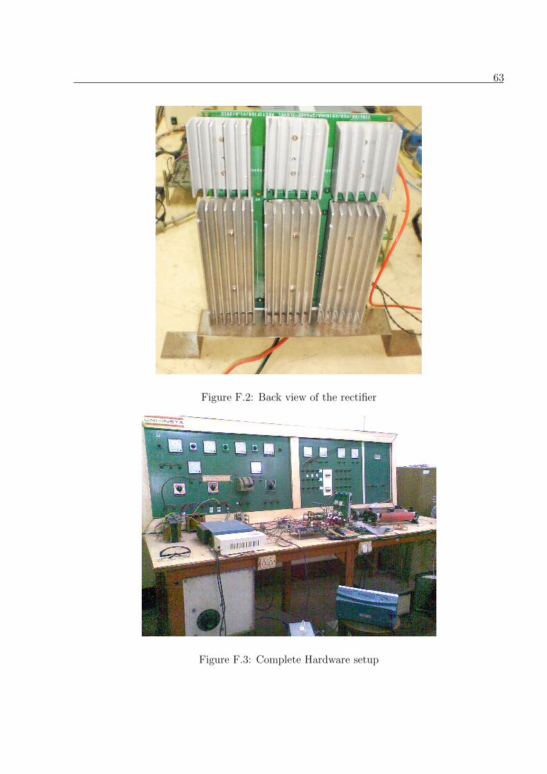
Pictures of the Hardware Setup
Figure F.1: Front view of the rectifier
62
63
Figure F.2: Back view of the rectifier
Figure F.3: Complete Hardware setup
References
[1] IEEE Standard 519-1992, IEEE Recommended Practices and Requirements for Harmonic
Control in Electrical Power Systems
[2] Kolar, J.W.; Zach, F.C.; , “A novel three-phase utility interface minimizing line current
harmonics of high-power telecommunications rectifier modules,” IEEE Transactions on
Industrial Electronics, vol.44, pp.456-467, August 1997
[3] Kolar, J.W.; Drofenik, U.; Zach, F.C.; , “Space vector based analysis of the varia-
tion and control of the neutral point potential of hysteresis current controlled three-
phase/switch/level PWM rectifier systems,” Proceedings of 1995 International Confer-
ence on Power Electronics and Drive Systems, vol.1, pp.22-33, February 1995
[4] Kolar, J.W.; Drofenik, U.; Zach, F.C.; , “Current handling capability of the neutral point
of a three-phase/switch/level boost-type PWM (VIENNA) rectifier,” 27th Annual IEEE
conference, Power Electronics Specialists Conference, vol.2, pp.1329-1336, June 1996
[5] Zhao, Y.; Li, Y.; Lipo, T.A.; , “Force commutated three level boost type rectifier,”
Conference Record of the 1993 IEEE Industry Applications Society Annual Meeting, vol.2,
pp.771-777, October 1993
[6] Singh, B.; Singh, B.N.; Chandra, A.; Al-Haddad, K.; Pandey, A.; Kothari, D.P.; , “A
review of three-phase improved power quality AC-DC converters,” IEEE Transactions
on Industrial Electronics, vol.51, pp.641- 660, June 2004
[7] Kolar, J.W.; Ertl, H.; Zach, F.C.; , “Design and experimental investigation of a three-
phase high power density high efficiency unity power factor PWM (VIENNA) rectifier
employing a novel integrated power semiconductor module,” IEEE Conference Proceed-
ings 1996, vol.2, pp.514-523, March 1996
64

References 65
[8] LTSpice IV, Linear Technology corporation, http://www.linear.com/software
[9] Vinod John, “Course Notes on Topics in power electronics and distributed generation”,
Department of Electrical Engineering, Indian Institute of Science, Bangalore, 2011
[10] G Narayanan, “Course Notes on PWM Converters and Applications”, Department of
Electrical Engineering, Indian Institute of Science, Bangalore, 2011
[11] PEG, “Hardware design, documentation of 3φ, 10kVA Inverter, Department of Electrical
Engineering, Indian Institute of Science, Bangalore, June 2003.
[12] IPC-2221, “Generic standard on printed board design”, The institute for interconnecting
and packaging electronic circuits, February 1998.
[13] Chung S K, “Phase locked loop for grid-connected three-phase power conversion sys-
tem”, Proc. IEE Electr. Power Appl., vol.147, pp 213-219, May 2000
[14] Drofenik, U.; Kolar, J.W.; , “Comparison of not synchronized sawtooth carrier and
synchronized triangular carrier phase current control for the VIENNA rectifier I,” IEEE
International Symposium on Industrial Electronics, vol.1, pp.13-19, 1999
[15] Hag-Wone Kim; Byung-Chul Yoon; Kwan-Yuhl Cho; Byung-Kuk Lim; Soon-Sang
Hwang; , “Single carrier wave comparison PWM for Vienna rectifier and consideration for
DC-link voltage unbalance of offset voltage effects,” IEEE Telecommunications Energy
Conference, pp.1-6, October 2011
[16] TMS320LF/LC240xA, “DSP Controllers Reference Guide”, Texas Instruments Inc.,
May 2006
[17] Internet, “Datasheets of various components and IC’s”