design of 16 bit arithmetic and logical unit using vivado ...ijsrset.com/paper/1843.pdf · various...
TRANSCRIPT

IJSRSET162510 | Received :06Sep2016 | Accepted :03 October 2016 | September-October-2016 [(2)5: 143-149]
© 2016 IJSRSET | Volume 2 | Issue 5 | Print ISSN: 2395-1990 | Online ISSN : 2394-4099 Themed Section: Engineering and Technology
143
Design of 16 bit Arithmetic and Logical Unit Using Vivado 14.7
and Implementation on Basys 3 FPGA Board
Prachi Sharma1, G. Rama Laxmi2, Arun Kumar Mishra3
1Student, EC Department, Bhabha College of Engineering, Bhopal, India
2,3Assistant Professor, EC Department, Bhabha College of Engineering, Bhopal, India
ABSTRACT
This paper primarily deals with the construction of arithmetic Logic Unit (ALU) using Hardware Description
Language (HDL) using Xilinx Vivado 14.7 and implement them on Field Programmable Gate Arrays (FPGAs) to
analyze the design parameters. ALU of digital computers is an aspect of logic design with the objective of
developing appropriate algorithms in order to achieve an efficient utilization of the available hardware. The
hardware can only perform a relatively simple and primitive set of Boolean & arithmetic operations and are based
on a hierarchy of operations that are built by using algorithms employing the hardware. Speed, power and utilization
of ALU are the measures of the efficiency of an algorithm. In this paper, we have simulated and synthesized the
various parameters of ALUs by using VHDL on Xilinx Vivado 14.7 and Basys 3 Artix 7 FPGA board.
Keywords : FPGA, ALU, XILINX Vivado 14.7, Basys 3 Artix 7 FPGA Board
I. INTRODUCTION
The Design and implementation of FPGA based
Arithmetic Logic Unit is of core significance in digital
technologies as it is an integral part of central
processing unit. ALU is capable of calculating the
results of a wide variety of basic arithmetical and
logical computations. The ALU takes, as input, the data
to be operated on (called operands) and a code, from the
control unit, indicating which operation to perform. The
output is the result of the computation. Designed ALU
will perform the following operations:
Arithmetic operations
Bitwise logic operations
All the modules described in the design are coded using
VHDL which is a very useful tool with its degree of
concurrency to cope with the parallelism of digital
hardware. The top level module connects all the stages
into a higher level at Register Transfer Logic (RTL).
RTL describes the requirements of data and control
units in terms of digital logic to execute the desired
operations. Each instruction from the architecture's
instruction set is defined in detail in the RTL. Once
identifying the individual approaches for input, output
and other modules, the VHDL descriptions are run
through a VHDL simulator and then is downloaded the
design on FPGA board for verification.
As FPGA has an application that it can incorporates
much logic on a single FPGA. So as floating point ALU
has many operations to be performed in the computer
we are using an FPGA IC to implement it. The
operations performed by the FPU are addition,
subtraction, multiplication, division and logical
operations as AND, OR, NOT etc. FPU mainly work on
Real as well as integers value.FPGA is an integrated
circuit designed to be configured by the customers or
designer after manufacturing- hence “Field
Programmable”. The FPGA configuration is generally
specified using a hardware description language, similar
to that used for an application specific integrated circuit
(ASIC).
FPGA contain programmable logic components called
“Logic Blocks”, and a hierarchy of reconfigurable
International Journal of Scientific Research in Science, Engineering and Technology (ijsrset.com)
144
interconnects that allows the block to be wired together.
Logic blocks can be configured to perform complex
combinational function or merely simple logic gates like
AND and OR. In most FPGA’s, the logic blocks also
include memory elements which may be simple flip
flops or more complete blocks of memory.
Figure 1. Symbol of 16-bit ALU
II. METHODS AND MATERIAL
1. Design of Top Level (RTL) Vhdl Module of 8 -
Bit Arithmetic Logical UNIT (ALU)
High level design methodology allows managing
thedesign complexity in a better way and reduces the
designcycle. [10]. A high-level model makes the
description andevaluation of the complex systems easier.
RTLdescription specifies all the registers in a design,
and thecombinational logic between them. The registers
aredescribed either explicitly through
componentinstantiation or implicitly through inference
[3]. Thecombinational logic is described by logical
equations,sequential control statements subprograms, or
throughconcurrent statements [3]. Designing at a higher
level ofabstraction delivers the following benefits [10].
Manages complexity: Fewer lines of code
improves productivity and reduces error.
Increases design reuse: Implementation of
independent designs as cell library & reuse in
various models.
Improves verification: Helps to run process faster.
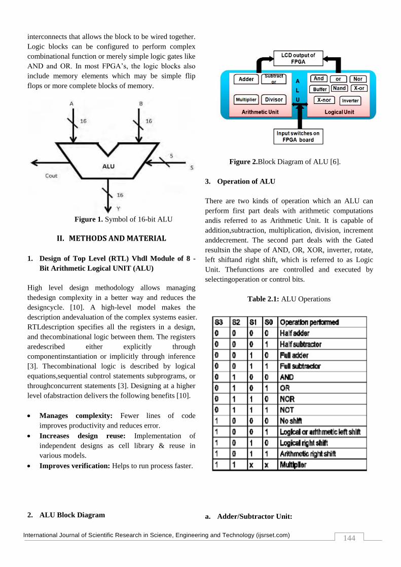
2. ALU Block Diagram
Figure 2.Block Diagram of ALU [6].
3. Operation of ALU
There are two kinds of operation which an ALU can
perform first part deals with arithmetic computations
andis referred to as Arithmetic Unit. It is capable of
addition,subtraction, multiplication, division, increment
anddecrement. The second part deals with the Gated
resultsin the shape of AND, OR, XOR, inverter, rotate,
left shiftand right shift, which is referred to as Logic
Unit. Thefunctions are controlled and executed by
selectingoperation or control bits.
Table 2.1: ALU Operations
a. Adder/Subtractor Unit:

International Journal of Scientific Research in Science, Engineering and Technology (ijsrset.com)
145
In our ALU we have used the concept of adder-
subtractor where the same circuit performs the functions
of both adder and subtractor as shown in fig 3. The
adder functions based on the concept of look ahead
carry adder. The subtractor just uses anxor gate as an
extra circuitry
The block diagram for an adder-subtractor circuit thus
can be as below. To perform this we used carry look
ahead adder, The carry look ahead adder reduces the
consumption of power without compromising the speed
of the adder [2]. This is achieved by generating carry
simultaneously from all the bits. An n-bit carry look-
ahead adder is formed from n stages. Carry look-ahead
can be extended to larger adders. For example, four 1bit
adders can be connected to form a 4bit adder and such
four 4-bit adders can be connected to form the 16-bit
adder.
Figure 3.Adder/Subtractor Unit
The use of a single circuit for both adder and subtractor
reduces power consumption and also area. The
operation of the adder-subtractoris based on the S1 and
S0 control bits.
Table 2.2: Operations of adder/subtractor circuit
b. Logic Unit:
Fig 4 shows the logic unit in ALU, which performs 4
different logical operations AND, OR, XOR and NOT
operations. Bitwise operation is performed on the two
inputs. The operation to be performed is decided by two
selections s1 and so as shown in Table 2.3.
Figure4.Logic Unit
Table 2.3: Logical Operations
C. Shifter Unit:
Logical shift is an efficient way to perform division and
multiplication of integers by powers of two. Shifting left
by k bits on a binary number is equivalent to
multiplying it by 2k.Similarly shifting right by k bits on
an binary number is equivalent to dividing it by 2k. For
example, consider the binary number 0001 0111.
Arithmetic shifts
Arithmetic shifts can be useful as efficient ways of
performing multiplication or division of signed integers
by powers of two. Shifting left by n bits on a signed or
unsigned binary number has the effect of multiplying it
by 2n. Shifting right by n bits on a two's complement
signed binary number has the effect of dividing it by 2n,
but it always rounds down (towards negative infinity).

International Journal of Scientific Research in Science, Engineering and Technology (ijsrset.com)
146
Arithmetic left shift [6] move bits to the left, same order
throw away the bit that pops off the MSB introduce a 0
into the LSB. This is same as logical left shift. It is
shown in figure 5. Arithmetic right shift move bits to
the right, same order throw away the bit that pops off
the LSB reproduce the original MSB into the new MSB
as shown in figure 6.
Figure5 :Arithmetic Left Shift
Figure 6 :Arithmetic Right Shift
Logical Shifts
Logical shift is a bitwise operation that shifts all the bits
of its operand. The two base variants are the logical left
shift and the logical right shift. This is further
modulated by the number of bit positions a given value
shall be shifted, like "shift left by 1" or a "shift right by
n". Unlike an arithmetic shift, a logical shift does not
preserve a number's sign bit or distinguish a number's
exponent from its mantissa; every bit in the operand is
simply moved a given number of bit positions, and the
vacant bit-positions are filled in, usually with zeros [7].
Logical left shift move bits to the left, same order throw
away the bit that pops off the MSB introduce a 0 into
the LSB as shown in figure 7. Logical right shift move
bits to the right, same order throw away the bit that pops
off the LSB introduce a 0 into the MSB as shown in
figure 8.
Figure7.Logical Left Shift
Figure 8.Logical Right Shift
Fig 9 shows the diagram of Shifter unit which performs
arithmetic/Logical, Right and Left shifts by using
Multiplexer and table 2.4 shows shifter operations
controlled by 2 selection lines s1 and s0.
Figure9.Shifter Unit
Table 2.4: Shifter unit Operations
International Journal of Scientific Research in Science, Engineering and Technology (ijsrset.com)
147
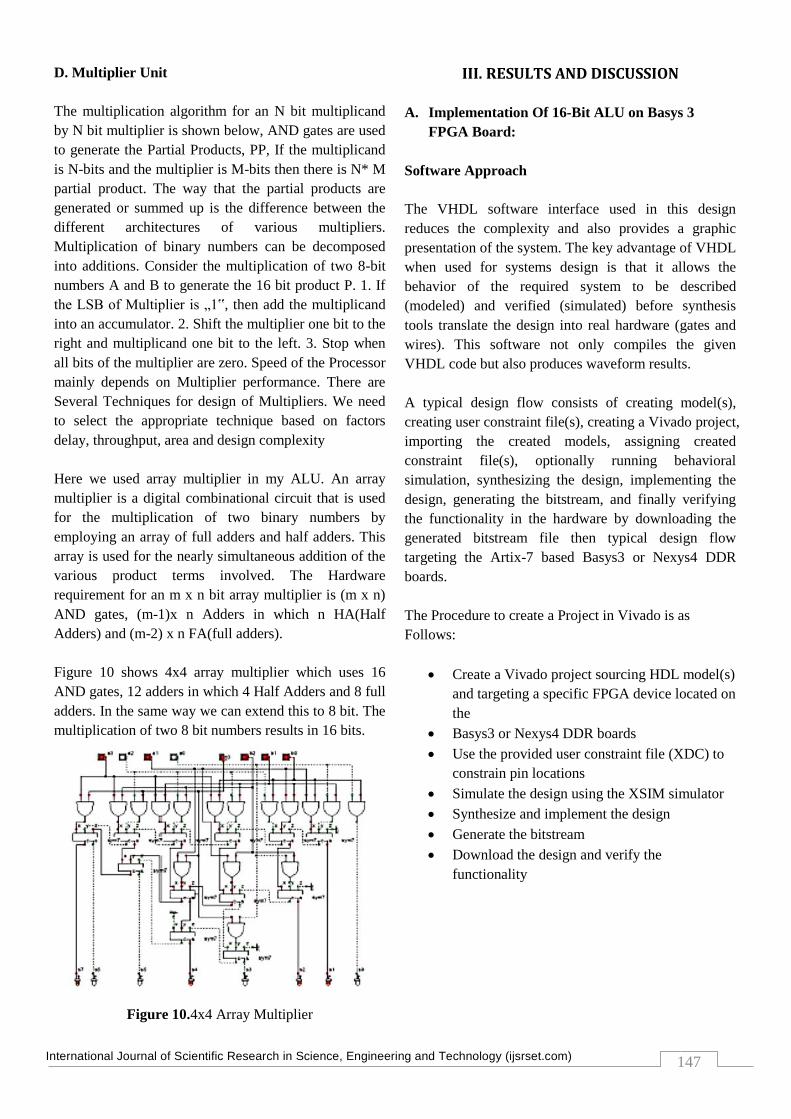
D. Multiplier Unit
The multiplication algorithm for an N bit multiplicand
by N bit multiplier is shown below, AND gates are used
to generate the Partial Products, PP, If the multiplicand
is N-bits and the multiplier is M-bits then there is N* M
partial product. The way that the partial products are
generated or summed up is the difference between the
different architectures of various multipliers.
Multiplication of binary numbers can be decomposed
into additions. Consider the multiplication of two 8-bit
numbers A and B to generate the 16 bit product P. 1. If
the LSB of Multiplier is „1‟, then add the multiplicand
into an accumulator. 2. Shift the multiplier one bit to the
right and multiplicand one bit to the left. 3. Stop when
all bits of the multiplier are zero. Speed of the Processor
mainly depends on Multiplier performance. There are
Several Techniques for design of Multipliers. We need
to select the appropriate technique based on factors
delay, throughput, area and design complexity
Here we used array multiplier in my ALU. An array
multiplier is a digital combinational circuit that is used
for the multiplication of two binary numbers by
employing an array of full adders and half adders. This
array is used for the nearly simultaneous addition of the
various product terms involved. The Hardware
requirement for an m x n bit array multiplier is (m x n)
AND gates, (m-1)x n Adders in which n HA(Half
Adders) and (m-2) x n FA(full adders).
Figure 10 shows 4x4 array multiplier which uses 16
AND gates, 12 adders in which 4 Half Adders and 8 full
adders. In the same way we can extend this to 8 bit. The
multiplication of two 8 bit numbers results in 16 bits.
Figure 10.4x4 Array Multiplier
III. RESULTS AND DISCUSSION
A. Implementation Of 16-Bit ALU on Basys 3
FPGA Board:
Software Approach
The VHDL software interface used in this design
reduces the complexity and also provides a graphic
presentation of the system. The key advantage of VHDL
when used for systems design is that it allows the
behavior of the required system to be described
(modeled) and verified (simulated) before synthesis
tools translate the design into real hardware (gates and
wires). This software not only compiles the given
VHDL code but also produces waveform results.
A typical design flow consists of creating model(s),
creating user constraint file(s), creating a Vivado project,
importing the created models, assigning created
constraint file(s), optionally running behavioral
simulation, synthesizing the design, implementing the
design, generating the bitstream, and finally verifying
the functionality in the hardware by downloading the
generated bitstream file then typical design flow
targeting the Artix-7 based Basys3 or Nexys4 DDR
boards.
The Procedure to create a Project in Vivado is as
Follows:
Create a Vivado project sourcing HDL model(s)
and targeting a specific FPGA device located on
the
Basys3 or Nexys4 DDR boards
Use the provided user constraint file (XDC) to
constrain pin locations
Simulate the design using the XSIM simulator
Synthesize and implement the design
Generate the bitstream
Download the design and verify the
functionality

International Journal of Scientific Research in Science, Engineering and Technology (ijsrset.com)
148
Figure 11. Typical Design Flow
Hardware Approach
The VHDL code which implies the hardware part of
ALU is downloaded on FPGA processor using JTAG
cable interfacing PC and the hardware element. A final
point is that when a VHDL model is translated into the
"gates and wires" that are mapped onto a programmable
logic device i.e FPGA, and then it is the actual hardware
being configured, rather than the VHDL code being
"executed" as if on some form of a processor chip.
The Basys3 board is a complete, ready-to-use digital
circuit development platform based on the latest Artix-7
Field Programmable Gate Array (FPGA) from Xilinx.
With its high-capacity FPGA (Xilinx part number
XC7A35T-1CPG236C), low overall cost, and collection
of USB, VGA, and other ports, the Basys3 can host
designs ranging from introductory combinational
circuits to complex sequential circuits like embedded
processors and controllers. It includes enough switches,
LEDs, and other I/O devices to allow a large number of
designs to be completed without the need for any
additional hardware, and enough uncommitted FPGA
I/O pins to allow designs to be expanded using Diligent
Pmods or other custom boards and circuits.
The Artix-7 FPGA is optimized for high performance
logic, and offers more capacity, higher performance,
and more resources than earlier designs. Artix-7 35T
features include:
33,280 logic cells in 5200 slices (each slice
contains four 6-input LUTs and 8 flip-flops)
1,800 Kbits of fast block RAM
Five clock management tiles, each with a phase-
locked loop (PLL)
90 DSP slices
Internal clock speeds exceeding 450MHz
On-chip analog-to-digital converter (XADC).
Figure 12.The Basys3
The Basys3 also offers an improved collection of ports
and peripherals, including:
16 user switches.
16 user LEDs.
5 user pushbuttons.
4-digit 7-segment display.
Three Pmod connectors.
Pmod for XADC signals.
12-bit VGA output.
USB-UART Bridge.
Serial Flash.
Digilent USB-JTAG port for FPGA
programming and communication.
USB HID Host for mice, keyboards and
memory sticks.
The Basys3 works with Xilinx’s new high-performance
Vivado™ Design Suite. Vivado includes many new
tools and design flows that facilitate and enhance the
latest design methods. It runs faster, allows better use of
FPGA resources, and allows designers to focus their
time evaluating design alternatives. The System Edition
includes an on-chip logic analyzer, high-level synthesis
tool, other cutting-edge tools, and the free WebPACK
version allows Basys3 designs to be created at no
additional cost.
The design consists of some inputs directly connected to
the corresponding output LEDs. Other inputs are
logically operated on before the results are output on the
remaining LEDs as shown in Fig 13

International Journal of Scientific Research in Science, Engineering and Technology (ijsrset.com)
149
Figure 13.Completed Design
B. Simulation Result of 16 Bit ALU Design
OR Operation
Figure 12. Waveform of OR operation.
XOR Operation
Figure 13.Waveform of XOR operation
IV. CONCLUSION
This study helped to understand the complete flow of RTL
design, starting from designing a top level RTL module for
16-bit ALU using hardware description language, VHDL.
Verification of the designed RTL code using simulation
techniques, synthesis of RTL code to obtain gate level
netlist using Xilinx Vivado ISE tool and Arithmetic Logic
Unit was successfully designed andimplemented using
Very High Speed HardwareDescriptive Language and
Xilinx Basys 3 FieldProgrammable Gate Array.The
designed arithmetic unit operates on 32-bit operands. It can
be designed for 64-bit operands to enhance precision. It
can be extended to have more mathematicaloperations like
trigonometric, logarithmic and exponential functions.
Arithmetic unit has been designed to perform five
arithmetic operations, addition, subtraction, multiplication,
division and square root, on floating point numbers.
V. REFERENCES
[1] B. Stephen Brown, V.Zvonko, "Fundamentals of
digital logic with VHDL Design"2ndEdition,Mc Graw
Hill International Edition, 2005.
[2] Charles H.Roth, Jr., "Digital System Design using
VHDL", PWS Publishing Company, 2006.
[3] Douglas L. Perry, VHDL, third edition, McGraw-Hill,
pp. 60-63, 238, July 1999.
[4] Mark Zwolinski, "Digital System Design with VHDL",
Prentice Hall, 2000.
[5] Pedroni, "Digital Logic Design using VHDL".
[6] S.Kaliamurthy, R.Muralidharan, "VHDL Design of
FPGA Arithmetic Processor" International Conference
on Engineering and ICT, 2007.
[7] Prof. S. Kaliamurthy & Ms. U. Sowmmiya, "VHDL
design of arithmetic processor" ,Global Journals
Inc.(USA) , November 2011.
[8] Landauer, R., "Irreversibility and heat generation in the
computing process", IBM J.Research and
Development, vol. 5 (3): pp. 183-191, 1961.
[9] Bennett, C.H., "Logical reversibility of computation",
IBM J. Research and Development, vol. 17: pp. 525-
532, 1973.
[10] B. Raghu Kanth1, B. Murali Krishna2, G. Phani
Kumar3, J. Poornima4, K. Siva Rama Krishna " A
Comparitive Study Of Reversible Logic
Gates"International Journal of VLSI & Signal
Processing Applications, Vol.2,Issue 1, Feb 2012.
[11] Himanshu Thapliyal ,Nagarajan Ranganathan "A New
Reversible Design of BCD Adder " IEEE conference
on Design and automation, 2011 pp.1-4.
[12] Zhijin Guan, Wenjuan Li, Weiping Ding, Yueqin
Hang, Lihui Ni"An Arithmetic Logic Unit design
based on reversible logic gates "IEEE Pacific Rim
Conference on Communications, Computers and
Signal Processing (PacRim), 2011.
[13] Thapliyal H, Srinivas M.B, "Novel Reversible TSG
Gate and Its Application for Designing Components of
Primitive Reversible/Quantum ALU,"Fifth
International Conference on Information,
Communications and Signal Processing, 2006.
[14] H.Thapliyal,M.B Srinivas "Novel design and reversible
logic synthesis of multiplexer based full adder and
multipliers" 48th Midwest Symposium on Circuits and
Systems, 2005.