design of a mid-infrared cavity ring down spectrometer
TRANSCRIPT

Design of a Mid-infrared
Cavity Ring Down Spectrometer
PROEFONTWERP
TER VERKRIJGING VAN DE GRAAD VAN DOCTOR AANDE TECHNISCHE UNIVERSITEIT EINDHOVEN, OP GEZAGVAN DE RECTOR MAGNIFICUS, PROF.DR. M. REM, VOOREEN COMMISSIE AANGEWEZEN DOOR HET COLLEGEVOOR PROMOTIES IN HET OPENBAAR TE VERDEDIGENOP DINSDAG 26 JUNI 2001 OM 16.00 UUR
DOOR
MARCEL MAURICE HEMERIK
GEBOREN TE LEIDEN

De documentatie van het proefontwerp is goedgekeurd door de promotoren:
prof.dr.ir. G.M.W. Kroesen
en
prof.dr.ir. M.C.M. van de Sanden
CIP-DATA LIBRARY TECHNISCHE UNIVERSITEIT EINDHOVEN
Hemerik, Marcel Maurice
Design of a mid-infrared cavity ring down spectrometer / by Marcel Maurice HemerikEindhoven: Technische Universiteit Eindhoven, 2001, -Proefontwerp-ISBN 90-386-1799-2NUGI 812Trefwoorden: absorptie, gasontlading, infrarood, moleculen, spectroscopieSubject headings: absorption, discharge, infrared, molecular, spectroscopy
Ontwerp omslag: B. Mobach / TU/eDrukwerk: Universiteitsdrukkerij Technische Universiteit Eindhoven

Alles wat ik bereik, heb ik aan mezelf te danken.Ik ben een schakel in een keten, maar tochfunctioneer ik als een volmaakte eenheid.Ik probeer zo hoog mogelijk te klimmenEn tref mijn doelZeker en zonder aarzelen.Het leven is als een heerlijke reis voor mij.Altijd blijf ik zoekende, want iedere vraagleidt automatisch tot een volgende.Ik ben vooruitgang, verkenning en inzicht.Ik ben de bron en inspiratie van alle activiteit.
IK BEN DE RAT.
Uit: ’Chinese Astrologie’, door T. LauISBN 9021526255 Kosmos/Z&K Uitgevers b.v.


Contents
1 General introduction 11.1 Plasma or electrical discharge? . . . . . . . . . . . . . . . . . . . . . . . . . . 21.2 Chemically active discharges . . . . . . . . . . . . . . . . . . . . . . . . . . . 2
1.2.1 Etching discharges . . . . . . . . . . . . . . . . . . . . . . . . . . . . 31.2.2 Depositing discharges . . . . . . . . . . . . . . . . . . . . . . . . . . 3
1.3 Plasma diagnostics . . . . . . . . . . . . . . . . . . . . . . . . . . . . . . . . 61.4 The history of spectroscopy . . . . . . . . . . . . . . . . . . . . . . . . . . . . 61.5 Infrared spectroscopy . . . . . . . . . . . . . . . . . . . . . . . . . . . . . . . 7
1.5.1 Spectroscopy on silane discharges . . . . . . . . . . . . . . . . . . . . 111.6 Shortcomings of conventional optical diagnostics . . . . . . . . . . . . . . . . 131.7 Cavity Ring Down Spectroscopy . . . . . . . . . . . . . . . . . . . . . . . . . 151.8 Scope of this thesis . . . . . . . . . . . . . . . . . . . . . . . . . . . . . . . . 17
2 Design considerations 192.1 Introduction . . . . . . . . . . . . . . . . . . . . . . . . . . . . . . . . . . . . 202.2 The choice of light source . . . . . . . . . . . . . . . . . . . . . . . . . . . . . 202.3 The vacuum vessel . . . . . . . . . . . . . . . . . . . . . . . . . . . . . . . . 25
2.3.1 The existing vacuum vessel . . . . . . . . . . . . . . . . . . . . . . . 262.4 The discharge . . . . . . . . . . . . . . . . . . . . . . . . . . . . . . . . . . . 262.5 Data Acquisition . . . . . . . . . . . . . . . . . . . . . . . . . . . . . . . . . 282.6 The ring down cavity . . . . . . . . . . . . . . . . . . . . . . . . . . . . . . . 292.7 The mirrors . . . . . . . . . . . . . . . . . . . . . . . . . . . . . . . . . . . . 342.8 Summary and time schedule . . . . . . . . . . . . . . . . . . . . . . . . . . . 35
3 The mid-infrared cavity ring down spectrometer 373.1 Introduction . . . . . . . . . . . . . . . . . . . . . . . . . . . . . . . . . . . . 383.2 The ring down cavity . . . . . . . . . . . . . . . . . . . . . . . . . . . . . . . 38
3.2.1 The body of the cavity . . . . . . . . . . . . . . . . . . . . . . . . . . 383.2.2 The mirror mounts . . . . . . . . . . . . . . . . . . . . . . . . . . . . 393.2.3 The mirrors . . . . . . . . . . . . . . . . . . . . . . . . . . . . . . . . 41
3.3 The vacuum system . . . . . . . . . . . . . . . . . . . . . . . . . . . . . . . . 423.3.1 The vacuum vessel . . . . . . . . . . . . . . . . . . . . . . . . . . . . 423.3.2 The pumps . . . . . . . . . . . . . . . . . . . . . . . . . . . . . . . . 443.3.3 Gas supply . . . . . . . . . . . . . . . . . . . . . . . . . . . . . . . . 443.3.4 The PLC . . . . . . . . . . . . . . . . . . . . . . . . . . . . . . . . . 44
3.4 The discharge . . . . . . . . . . . . . . . . . . . . . . . . . . . . . . . . . . . 453.4.1 The manipulator . . . . . . . . . . . . . . . . . . . . . . . . . . . . . 46
i

3.5 The diode laser system . . . . . . . . . . . . . . . . . . . . . . . . . . . . . . 473.5.1 Basic principles of semiconductor diode lasers . . . . . . . . . . . . . 473.5.2 The helium cooled diode laser system . . . . . . . . . . . . . . . . . . 48
3.6 The detection branch . . . . . . . . . . . . . . . . . . . . . . . . . . . . . . . 493.7 Laser control and data acquisition . . . . . . . . . . . . . . . . . . . . . . . . 51
3.7.1 Description of the different parts . . . . . . . . . . . . . . . . . . . . . 523.7.2 Different modes of operation . . . . . . . . . . . . . . . . . . . . . . . 53
4 Characterization of the infrared diode laser beam 554.1 Introduction . . . . . . . . . . . . . . . . . . . . . . . . . . . . . . . . . . . . 564.2 The beam profiler . . . . . . . . . . . . . . . . . . . . . . . . . . . . . . . . . 564.3 The laser diode . . . . . . . . . . . . . . . . . . . . . . . . . . . . . . . . . . 574.4 The off-axis parabolic mirror . . . . . . . . . . . . . . . . . . . . . . . . . . . 574.5 The monochromator . . . . . . . . . . . . . . . . . . . . . . . . . . . . . . . . 66
5 Characterization of the mid-infrared cavity ring down spectrometer 715.1 Introduction . . . . . . . . . . . . . . . . . . . . . . . . . . . . . . . . . . . . 725.2 Characterization of the optical cavity with the CO laser . . . . . . . . . . . . . 725.3 The diode laser beam and the ring down cavity . . . . . . . . . . . . . . . . . 75
5.3.1 The mode structure with the diode laser . . . . . . . . . . . . . . . . . 755.3.2 Detuning the laser . . . . . . . . . . . . . . . . . . . . . . . . . . . . 775.3.3 The exponential decay . . . . . . . . . . . . . . . . . . . . . . . . . . 785.3.4 The first mid-infrared spectroscopic cavity ring down measurements . . 79
6 General conclusions 83
Bibliography 87
Summary 91
Samenvatting 93
Dankwoord 95
Curriculum vitae 96

1General introduction

2 Chapter 1
1.1 Plasma or electrical discharge?
Plasmas are often called ”the fourth state of matter”. Feeding energy to solid matter (e.g. ice)turns it first into a liquid (water) which, if the energy supply persists, can be evaporated into agas (water vapor). If even more energy is added, this gas can eventually be turned into a plasma.
Here on earth most plasmas are generated by electrical discharges. When an electricaldischarge is struck between two electrodes, ionisation processes start and positive ions and freeelectrons are created. Due to the higher mobility of the electrons, a space charge region isformed in the periphery of the discharge. In the equilibrium situation the central region willcontain a fraction (10−10- 1) of charged particles, but in total it will be quasi neutral. Thisquasi-neutral region is often referred to as a ”plasma”. The fact that a plasma is quasi-neutralmeans that it contains as many positively charged particles (positive ions) as negatively chargedparticles (negative ions and/or electrons).
Therefore, technically spoken, an electrical or gas discharge is the complete region betweenthe electrodes, including the space charge regions, while the plasma is limited to the quasi-neutral central region. In literature this difference is less strict, and also in this thesis we willnot make a distinction.
A good example of the effect a small fraction of ions and electrons can have on a gas isthe electrical discharge in a tubular fluorescent lamp. The glass tube of the lamp is filled withargon and a small fraction of mercury vapor. The electrodes at both ends of the tube inducean electric field that partially ionizes the mercury atoms. The positive mercury ions and freeelectrons are accelerated towards the electrodes and during their trip collide many times withneutral mercury atoms. During these collisions new ions and electrons can be created, whichis necessary for sustaining the discharge, or the mercury atoms can get into an excited state.When these excited mercury particles fall back to the ground state they emit photons. Althoughthe ionization degree is typically 10−6-10−5, in a tubular fluorescent lamp about 20 % of theelectric energy is converted into light.
A good example of a pure plasma is the sun. The sun, as all stars in the universe, is a bigcloud of gas and because of the high temperature inside, all of the gas is ionized. Most ofthe processes going on inside the sun could not happen without the presence of the chargedparticles.
The example of the discharge in a fluorescent lamp is a typical example of a non-chemicaldischarge. The buffer gas is a noble gas, e.g. argon, that does not react with the mercuryparticles. The mercury particles themselves do not undergo any chemical reaction either. Allthe basic processes going on in a fluorescent lamp can be considered to be physical processes.
1.2 Chemically active discharges
If the feed gas of the discharge contains molecules (e.g. hydrogen (H2)), the collisions in the dis-charge can, in addition to excitation and ionizition, also induce dissociation of these molecules(H2 → H + H). The fractions that are created in this way tend to chemically react with otherparticles they encounter. This can be other gas phase particles but also solid state matter likethe walls of the reactor. By choosing the feed gases one can create many different chemicallyactive discharges.

General introduction 3
1.2.1 Etching discharges
By taking feed gases that contain fluorine (e.g. CF4 or SF6) one creates a plasma that can etchlayers of e.g. silicon. These discharges are frequently used in the semiconductor industry toetch small scale structures in silicon wafers.
The complex chemistry formed by the combination of the ions and radicals impinging onthe substrate makes this etching process very anisotropic (Fig. 1.1) and very selective.
+
+
+
+ + +
+
+ +
+
+
+
+
+
+ +
+
+
+
+
+
+
+
+
+ +
+
+
+
+
+
+
+
+
mask
material A
material B
substrate
Fig. 1.1: (left) isotropic chemical etching and (right) anisotropic reactive ion etching.
1.2.2 Depositing discharges
Feed gases containing silicon atoms (e.g. silane (SiH4)) can be used to grow thin layers of siliconon substrates. This plasma enhanced chemical vapor deposition (PECVD) of silicon producessemiconducting layers of silicon atoms in an amorphous matrix (a-Si:H), where the danglingbonds are passivated by hydrogen atoms. This material is extensively used to produce thin filmtransistors (TFTs) for LCD applications, but in recent years a lot of interest has been going outto the solar cells that can be produced with it.
a-Si:H solar cells
Solar cells based on amorphous silicon consist of a stack of thin layers on a transparent (e.g.glass) substrate (Fig. 1.2). The central layer of the whole structure is the intrinsic a-Si:H layer.This layer is the active photovoltaic layer that collects the photons that enter the cell through theglass, and converts the photon energy into free electron-hole pairs. An n-type and p-type dopedlayer sandwich the intrinsic layer and create an electric field that draws the free charge carriersto the electrodes.
metalnegatively doped layer
intrinsic a-Si:H
positively doped layertransparent conductive oxide
glass
-
+
incoming light
Fig. 1.2: Cross section of an a-Si:H solar cell.

4 Chapter 1
A big advantage of a-Si:H over other materials used to make solar cells (e.g. crystalline sili-con), is the efficient absorption of photons within the solar spectrum, which makes the necessarythickness of the active layer much smaller than for those other materials.
However, although the absorption of photons is very efficient, the resulting cell efficiency,defined as the total electrical energy output divided by the energy input of the sun, remains verylow. Typical cell efficiencies at the moment the cell leaves the production plant are around 10%,but within a relative short time of exposure of the solar cell to the light of the sun, the efficiencydrops to about half the initial value. This light-induced degradation, called the Staebler-Wronskieffect, is one of the main factors that make the a-Si:H solar cells economically unattractive.
Another factor that makes the a-Si:H solar cell a mediocre candidate for future energy pro-duction is the low deposition rate of a-Si:H. This low deposition rate makes the resulting solarcell too expensive to compete with other energy sources. Fundamental research is needed toincrease the understanding of the elementary processes going on in the gas discharges used togrow the a-Si:H layers, to come to economically competitive solar cells [1][2].
Recently, a research group at the Ecole Polytechnique in Paris succeeded in fabricating ana-Si:H solar cell that did not show the Staebler-Wronski effect [3] (Fig. 1.3). Closer inspectionof the grown layers showed that nanosized crystalline structures were embedded in the intrinsica-Si:H layer. These crystalline nano-particles were thought to have grown in the discharge andwere kept responsible for the stability of the solar cell.
0 50 100 150 2000
2
4
6
8
10
pm Si
Effi
cien
cy (
%)
Time (hours)
He 250 oC
Std 250 oC
Std 150 oC
Std 100 oC
Fig. 1.3: Light induced degradation of a-Si:H solar cells made under different conditions.All cells show a rapid degradation, except for the pm -Si solar cell with the embeddednano-crystalites (black squares)

General introduction 5
The role of radicals during PECVD of a-Si:H
At the onset of the discharge the silane gas is dissociated by electron impact. The resultingparticles are mainly SiH3 and SiH2. In smaller amounts also SiH radicals and Si atoms areproduced. When these radicals hit a glass substrate, they have a reasonable chance of stickingto this substrate and starting the growth of a layer of silicon. Subsequent radicals should firstremove the hydrogen that now passivates the substrate to create new growth sites before otherradicals can attach to the substrate (Fig. 1.4).
(a) (b) (c)
Silicon
Hydrogen
(d)
Fig. 1.4: (left) (a) The first radicals arrive at a clean substrate and form the first monolayer ofa-Si:H. (b) Subsequent radicals find a hydrogen passivated surface and first have to removehydrogen atoms to create new growth sites (c), before new radicals can attach to the surfaceto form the next layer of silicon (d).
It is widely believed that SiH3 is the most important radical for the growth of a-Si:H, but theexact processes that remove hydrogen from the substrate are still not known. That these removalprocesses might be more important than the actual addition of silicon atoms to the surface isdemonstrated by a very simple calculation: Silane gas has four hydrogen atoms for each siliconatom, while device quality a-Si:H has only one hydrogen atom for every ten silicon atoms. Sofor each hydrogen atom that is embedded in the a-Si:H layer, about 39 hydrogen atoms have tobe removed from the discharge. Even if all the growth can be attributed to the SiH3 radical, 2.9hydrogen atoms remain to be removed for every radical that sticks to the surface.
The role of dust particles during PECVD
While the radicals near the substrate compete for free growth sites, the radicals inside the plasmavolume are free to react with any particle they collide with. Especially SiH2 is well known forits gas phase reactions. It effectively reacts with the silane gas itself to create Si2H5 and Si2H6.The Si2H5 molecule is a radical too, and is thought to be able to undergo the same reactionsas the mono-silane radicals. Si2H6 on the other hand is a stable particle but can react just likeSiH4 to form Si3Hx and so on. If these growing particles stay neutral they eventually will beremoved from the discharge by the gas flow, but if they obtain a negative charge during theinitial growth phase, they will be trapped inside the plasma volume. In this way large negativeions can be rapidly formed in the discharge that grow from tens of nanometers after one secondto micrometer sizes in a couple of minutes. The latest developments in the a-Si:H solar cellresearch suggest that the nanometer sized particles may have a beneficial influence on the finalsolar cell, while the larger particles are still regarded as a major threat to the thin layers, whichare only several hundreds of nanometers thick themselves.

6 Chapter 1
The influence of plasma parameters
Many groups all over the world dedicate a substantial part of their research to silane discharges.Despite all their efforts it has been impossible to clarify the processes in these discharges be-cause of one special reason. The balance between all the reactions inside the plasma volume andat the plasma-wall boundary is so delicate that a slight change in one of the external parameterslike feed gas composition, flow rate and temperature, electrode configuration and temperature,dissipated power etc. has a considerable influence on the resulting discharge. Therefore it is inmost cases not justified to compare experiments performed in one laboratory to the experimentsperformed in another laboratory.
1.3 Plasma diagnostics
In order to explain why a discharge behaves in the way it does, it is necessary to know theabsolute densities of all the particles in the discharge, including those near the plasma-wallinterface. One way of doing this could be to take a sample of the gas and analyze it, as isdone with a mass spectrometer. However, because of the size and shape of mass spectrometers,the instrument has to be mounted outside the plasma chamber and sample the gas through aorifice in either the chamber wall or one of the electrodes. Therefore it can only take samplesof the gas near the walls or electrodes and not from the plasma volume. Another problem arisesfrom the physical processes necessary to analyze the gas. These processes tend to change thecomposition of the gas sample and therefore make the translation of mass spectra into plasmacomposition very difficult.
An approach to measure densities inside the plasma volume would be to put some sort ofsampling device in the discharge. This is done with the Langmuir probe technique, where onemeasures the current through a probe as a function of the voltage applied over the probe. Fromthis I-V characteristic, in the ideal case one can deduce the electron and ion densities. However,this diagnostic is not suited for depositing discharges because the probe will be covered witha layer of a-Si:H in a matter of seconds, thereby destroying the probe’s initial characteristics.Furthermore, probes change one of the most essential properties of a discharge: the electricfield. It is therefore questionable if the measured densities are representative for the rest of thedischarge.
To avoid this kind of problems one needs another way to ’probe’ discharges.
1.4 The history of spectroscopy
As mentioned before, the sun is a plasma too and although we cannot sample it directly, nowa-days its composition is well known. This knowledge was obtained by studying the absorptionlines in the otherwise continuous spectrum of the sun.
Absorption lines arise from the fact that each element of the periodic table has its own dis-crete energy levels and thereby can only absorb or emit photons with certain energies. There-fore, these absorption lines serve as a set of fingerprints for the elements present in the studiedgas.
While studying the spectrum of the sun back in 1868, Sir Joseph Lockyer observed a set ofspectral lines that could not be associated with any known element on earth. He then postulated

General introduction 7
that these lines should belong to a new element, which from then on was called helium (derivedfrom the Greek word for sun: Helios). It took almost thirty years before Sir William Ramsaysucceeded to isolate enough helium on earth to confirm this hypothesis.Nowadays approximately 60 elements have been identified in the solar spectrum.
Absorption spectroscopy is just one way to make use of the discrete energy levels of atomsand molecules. Excited particles that fall back to a lower energy state can do this by emittinga photon. This results in a similar line spectrum, but now in emission. A third way is a kindof combination of the two methods described above. A particle in the ground state absorbs aphoton, which can be supplied by e.g. a laser, and is excited to a high energy level. From thishigh energy level it can de-exite to another, lower, energy level. This de-excitation can takeplace by emitting a photon: the fluorescence radiation. This technique is called laser inducedfluorescence (LIF).
1.5 Infrared spectroscopy
The atomic energy levels find their origin in the orbits of the bound electrons around the nucleusof the atom. The transition of an electron from one orbit to another involves energies of aboutone to twenty eV, which corresponds to the spectral range from the near infrared to the VUV.
Molecules, on the other hand, show fine structures on these spectra that cannot be explainedby their electronic levels. Because of the finite masses and sizes of the atoms and bindingstrengths between the atoms, a molecule can vibrate and rotate. Each atom in a molecule hasthree degrees of freedom. This results in 3N degrees of freedom for a N-atomic molecule.Three degrees of freedom are spent on the three translational directions of the molecule andtwo or three on the rotational movements, depending on the linearity of the molecule. Thisleaves 3N-6 (3N-5 for linear molecules) degrees of freedom, resulting in the same number offundamental vibrational modes (Fig. 1.5).
1 3
Fig. 1.5: The three fundamental vibrational modes of a non-linear 3-atomic molecule likeH2O or SiH2; (ν1) symmetrical stretch, (ν2) bending, and (ν3) asymmetric stretch.
Quantum mechanics predicts that the vibrational and rotational energies are also quantized,just like the electronic energy. When an electronic transition occurs in a molecule, also thevibrational and rotational states can change within discrete energy levels, giving rise to finestructures. Changes in vibrational and rotational states can also occur without an electronictransition, leading to spectra in the infrared.

8 Chapter 1
Vibrational transitions
The simplest case to illustrate the appearance of vibrational spectra is the diatomic molecule[4]. It may be represented by two masses, m1 and m2, connected by a spring. For smalldisplacements s from the equilibrium position Hooke’s law (f = −ks) can be applied, whichleads to a parabolic potential energy:
E = 12ks2, (1.1)
where k is the force constant. The quantum mechanical Hamiltonian for this simplified systemis given by
H = − h2
2µ
∂2
∂s2+ fs2, (1.2)
with µ = m1m2/(m1 +m2) the reduced mass of the system, h = h/2π and h the Planck con-stant. The eigen values of the Schrodinger equationHΨ = EΨ give the quantisized vibrationalenergy levels:
Eν = (ν + 12)ω
ccm−1, (1.3)
where ν is the vibrational quantum number, ω is the angular frequency, and the speed of light cis taken in cm/s, in order to come to the unit cm−1, which is the most commonly used unit forenergy in vibrational and rotational spectroscopy.
If the molecule has a permanent dipole moment, interaction with radiation can induce atransition from one vibrational state to another. Further evaluation of the Schrodinger equationleads to the selection rule for the allowed transitions: ∆ν = ±1 . A better but more complicatedapproach would be to treat the molecule as an anharmonic oscillator [5]. This leads to the morerealistic selection rules where ν can change by more than one unit
∆ν = ±1,±2,±3, .... (1.4)
When the vibrational energy levels are not degenerate, the relative distribution over the energylevels is determined by the Boltzmann distribution:
Nν
N0
= exp
(−νω hc
kTvib
), (1.5)
with N0 the density of the vibrational ground state, Nν the density of the state correspondingto vibrational quantum number ν, and Tvib the vibrational temperature. At room temperaturekTvib/hc ≈ 200 cm−1, which is much smaller than the spacing between vibrational levelsof diatomic molecules (1000 - 4000 cm−1). Therefore, at room temperature, almost all themolecules are in the vibrational ground state. In a discharge the vibrational temperature can besubstantially higher, which leads to a considerable change in the distribution over the differentlevels.
Rotational transitions
For the treatment of the rotational part of the spectrum the diatomic molecule can be consideredas two masses separated by a constant average distance r0. The molecule rotates around itscentre of gravity and has a moment of inertia:
I =m1m2
m1 +m2r2
0 = µr20. (1.6)

General introduction 9
The use of the Schrodinger equation with the Hamiltonian for a rigid diatomic moleculeleads to the following rotational energy levels:
EJ = BJ(J + 1), (1.7)
with J the rotational quantum number, and B the rotational constant:
B =h
8π2Iccm−1, (1.8)
where the speed of light c is again expressed in cm/s. For large quantum numbers J, the distancebetween the atoms increases, which causes a decrease of the rotational constant (∼ 1/r2). Thiscan be accounted for by adding an extra factor to Eq. 1.8:
EJ = BJ(J + 1)−DJ2(J + 1)2, (1.9)
with D a correction term in the order of 10−3B, which makes it negligible for small J’s. Theselection rules resulting from the Schrodinger equation impose that for linear molecules therotational quantum number can only change by one unit (∆J = ±1). For nonlinear moleculesalso vibrational transitions without a change in rotational quantum number are allowed, whichleads to the general selection rule (Fig. 1.6):
∆J = 0,±1. (1.10)
The distribution over the different levels can again be derived from the Boltzmann distri-bution, but, because of the degeneracy in the energy states (e.g. (2J + 1)-fold degeneracy forlinear molecules) an extra factor appears in front of the exponent:
NJ
N0= (2J + 1) exp
(−J(J + 1)B
hc
kTrot
). (1.11)
Because of this degeneracy and the fact thatB kTrot/hc the maximum of this distributionis not located at the J = 0 level but at a level with a much higher quantum number J .
J = -1 J = 0 J = +1
P Q R
= 0
= 1
…321
J = 0
…3210
Fig. 1.6: The allowed rotational transitions for a vibrational transition from the ground state

10 Chapter 1
Interaction of rotation and vibration
When the selection rules for vibrational and rotational transitions are combined (Eqs. 1.4 and1.10) and taking into account that most molecules are in their vibrational ground state and inan arbitrary rotational state, it becomes possible to calculate the rovibrational energy levels of amolecule:
∆E =ω
c+B′J ′(J ′ + 1)−B′′J ′′(J ′′ + 1). (1.12)
Since the average distance between the atoms is larger for a molecule in the vibrational upperlevel (denoted with a prime) than for a molecule in the vibrational lower level (denoted with adouble prime), the rotational constant will be smaller for the upper level. Using the generalselection rules for rotational transitions (Eq. 1.10), make that the spectrum can be divided inthree parts, the P-, Q-, and R-branch:
P-branch :∆J = −1⇒ J ′ = J ′′−1⇒ ∆E = ω
c−J ′′(B′′+B′)−J ′′2(B′′−B′). Since B′′ > B′ both the
term linear and quadratic in J ′′ give a negative contribution. Therefore the P-branch extends tothe left of the vibrational transition (ω/c), and the distance between the levels increases slowlywith increasing quantum number J.
Q-branch :∆J = 0⇒ J ′ = J ′′ ⇒ ∆E = ω
c−J ′′(B′′−B′)−J ′′2(B′′−B′). Again both contributions are
negative but because of the small difference between B ′′ and B′ both contributions are small.Therefore the Q-branch is also located to the left of the vibrational transition but stays muchcloser to the band origin.
R-branch :∆J = +1⇒ J ′ = J ′′ + 1⇒ ∆E = ω
c− J ′′2(B′′−B′)− J ′′(B′′− 3B′) + 2B′. The R-branch
starts on the right of the band origin, with a decreasing line spacing for increasing J. At a certainpoint the net contribution becomes negative and the lines for higher J’s are located nearer to theband origin or can even be located to the left of it.
If the rotational constants B for all the different rotational quantum numbers J and vibra-tional states ν are known, the above expressions can be represented in a Fortrat diagram (Fig.1.7). The parabolas in the upper part of Fig. 1.7 represent the energies of the different branchesfor non-integer values of J . The drawn circles are the intersections of theses parabolas withinteger values of J . Those intersections give the energies of the spectral lines of the differentbranches. Combining the different branches gives the total rovibrational spectrum. A goodexample of a real rovibrational spectrum is the silane spectrum in Fig. 1.8.
Hot bands
From the Boltzmann distribution (Eq. 1.5), it follows that for vibrational transitions with lowenergies or for high vibrational temperatures, a considerable part of the molecules will be in avibrational excited state. The molecules in the excited states have similar, but slightly shiftedrovibrational spectra, which are called hot bands.

General introduction 11
15 -
10 -
5 -
0 -
J
E (cm )-1/c
P-branch
Q-branch
R-branch
combinedspectrum
E (cm )-1
origin
Fig. 1.7: Impression of a Fortrat diagram.
1.5.1 Spectroscopy on silane discharges
SiH4
When interest in silane discharges arose, the electronic transitions of most particles in thesedischarges had not been identified yet. Therefore, several research groups started investigatingthe infrared spectra of the different species. The infrared spectrum of SiH4 was well knownwith the very distinct P, Q and R-branches around 2180 cm−1[6] (Fig. 1.8). The extensive highresolution measurements in 1978 by Cabana et al. [7] created a good spectroscopic reference.
2000 2050 2100 2150 2200 2250 2300
Wavenumber cm -1
R-branch
Q-branch
P-branch
Fig. 1.8: Rotation-vibration spectrum of silane around 2180 cm−1. Although the differentbranches are clearly visible, the individual lines can not be discerned due to the limitedresolving power of the used FTIR-spectrometer.
12 Chapter 1
SiH
The SiH radical always gained a lot of interest because of its abundance in interstellar material.It was the first silane radical to be spectroscopically detected. In 1957 Douglas [8] measuredan absorption spectrum in the visible part of the spectrum. In 1965 Verma reported new bandsystems in the UV [9] and in 1967 Herzberg published electronic transitions in the VUV [10].
But it was not until 1982 that Knights et al. [11] observed infrared emission lines of theSiH radical in their high resolution Fourier transform infrared (FTIR) spectrometer. The linesthey reported were centered around 1970 cm−1. Three years later Davies et al. used an infrareddiode laser system to improve those measurements and they detected, besides the fundamentalband, also some hot band transitions [12].
SiH2
In 1968 Dubois succeeded in photographing the absorption spectrum of SiH2 (silylene) in thevisible [13] and was able to determine some of the vibrational and rotational constants of thisradical. It took seventeen years before Fredin et al. could measure the infrared spectra of SiH2
molecules trapped in low temperature argon matrices and confirm these findings [14]. Thevibrational frequencies thus found were 1992.8, 1973.3, 1964.4, and 994.6 cm−1. In 1989Yamada et al. [15] succeeded to observed the ν2 band of this radical for the first time in the gasphase by using an infrared diode laser.
SiH3
Although by far the most interesting radical in silane discharges, due to the complete lack ofknown electronic transitions it was not until 1985 that Yamada and Hirota [16] reported the firstpositively identified spectra of SiH3 (silyl) in the infrared. They used an infrared diode laser toobserve the ν2 band around 727.9 cm−1and were able to derive some of the molecular constants.
Not much later Sumiyoshi et al. [17] recorded the high resolution absorption spectrum of theν3 band around 2185 cm−1. In 1991 Lightfoot et al. measured an absorption peak of the SiH3
radical in the UV around 215 nm [23]. Toyoda et al. used this absorption feature to measureSiH3 radicals and particulates [24]. Boogaarts et al. applied the cavity ring down detectionscheme on this absorption feature to measure SiH3 densities in the hostile environment of adepositing plasma [25].
Although the measurements are straightforward, the analysis of the data is quite difficult.The absorption peak has a diffusive feature that is attributed to the dissociative tendency of theexcited states. Moreover, dust particles grown in the discharge considerably scatter the UV lightso that the SiH3 absorption signal is superposed on the background scattering signal.
SiH+/−3
Of considerable interest for plasma physics are the ionic species. In 1990 Shen et al. usedquantum mechanical methods to predict some vibrational frequencies for the silyl anion (SiH−3 )around 2000 cm−1[26]. In 1992 Smith et al. measured many vibration-rotation lines of the ν2
band of the silyl cation (SiH+3 ) around 838 cm−1[27].

General introduction 13
Si2H6
When Finholt et al. [18] discovered a convenient method to prepare disilane (Si2H6) in 1947,Gutowsky and Stejskal started to investigate its infrared absorption spectrum. In 1953 theyreported four of the five infrared active fundamentals between 350 and 4000 cm−1[19]. Theabsorption bands they found were centered around 842.7, 945.7, 2154.4, and 2181.1 cm−1.
Hamilton and Vaghjiani reported the high-resolution spectra of the ν6 band around 842.7cm−1 in 1992 [20] and the ν8 band around 939.3 cm−1 in 1993 [21]. Also in 1992 McKeananalyzed the ν7 band of disilane around 2169 cm−1 [22].
Other radicals
Closer inspection of the infrared spectra of the silane radicals reveals that they can be separatedinto two groups. One group of absorption lines between ca. 700 and 1000 cm−1 and one groupbetween 1800 and 2400 cm−1. This is no coincidence. The frequencies between 700 and 1000cm−1 correspond to the bending vibrations of the Si-H bonds and the bands around 2000 cm−1
to the stretching vibrations. The quantum-mechanical Hamiltonian, from which the fundamen-tal frequencies can be derived, is primarily determined by the mass of the molecule and thebinding strengths. In mono-silane molecules the mass of the molecule is mostly determininedby the silicon atom, while the number of hydrogen atoms gives only a slight change. Largermolecules like Si2Hx or Si3Hx can be seen as chains of silicon atoms terminated by SiH2 orSiH3 groups. It is therefore very likely that other, undetected, radicals have infrared absorptionspectra in these regions too. Recent calculations have already shown that the Si2H5 radical hasabsorption bands around 2300 cm−1.
1.6 Shortcomings of conventional optical diagnostics
A technique which can avoid the disadvantages of mass spectroscopy and Langmuir probes isoptical spectroscopy. In principle, it is a non-intrusive technique with great possibilities forspatially and time resolved measurements. By using the complete electromagnetic spectrumfrom the extreme UV to the far infrared it is possible to detect a great number of differentspecies. However, several complications make that it is still impossible to unravel the chemicaldynamics of e.g. silane discharges.
This is mostly caused by the low number densities of the different radicals, which makes itimpossible to detect them in a straightforward manner in ’normal’ discharges. There are twogeneral solutions to increase the signal to noise ratio:
1. The most direct way to increase the signal to noise ratio is to increase the optical pathlength through the discharge. This can be done by implementing a multi-pass cell. Multi-pass cells consist of a number of mirrors, which are cleverly placed around the dischargeto reflect the optical beam several times through the discharge before it reaches the de-tector. The best multi-pass cells can reflect the beam approximately one hundred times,but since the signal to noise ratio only increases with the square root of the number ofpasses, the advantage is only moderate. In most cases this advantage does not balance thedisadvantages:

14 Chapter 1
• The great number of passes through the discharge make spatially resolved measure-ments impossible. Since spatial resolution was one of the main advantages of opticalspectroscopy, this is a great loss.
• To allow the optical beam to pass the discharge many times, a few large aperturesor many small apertures have to be made in the walls of the plasma reactor. Thesemandatory apertures in the discharge chamber tend to change the gas flow and theplasma-wall interaction, and thereby the chemistry of the discharges.
2. The second way is to decrease the noise level. This can be done by time integrating oraveraging a number of measurements. Again, the signal to noise ratio only increases withthe square root of the number of averages or the increase in sampling time. So, to reachan adequate increase, a large number of averages has to be made. The advantage of theincreased signal to noise ratio is often outweighed by the disadvantages of this method:
• Again, the sensitivity is increased at the cost of one of the main advantages of thediagnostic: the time resolution. Since time resolved measurements offer essentialinsights in complex chemical discharges, this is an undesirable side effect.
• Some species only exist for very short times, e.g. the growth precursors of dustparticles. For this kind of species, the increase in measurement time can actuallydecrease the signal to noise ratio.
When neither the multi-pass cell, nor time averaging gives the necessary increase in signal tonoise ratio, a combination of the two measures might offer a solution. But of course, this canonly be accomplished at the cost of both the time resolution and the spatial resolution.
And if even this does not have the desired effect, the last solution is to look for ways to in-crease the density of the radical to be measured. This can be done by changing the compositionof the feed gases, the pressure, power or flow rate, or even building exotic discharge configu-rations that have nothing to do with the original discharge under investigation. Many researchgroups have built setups to detect one particle or another, but, because of the many differences indischarge configurations and feed gas compositions, none of these discharges were comparablewith each other.
It needs no further explanation that radical densities measured in these ways tell nothingabout the chemistry inside the plasmas used to grow solar cells.
The ability to accurately measure a small decrease in intensity typically limits the sensitivityto absorption losses of 10−2 to 10−3. The required signal stability can only be reached withhighly stable continuous lasers and the use of some sort of frequency modulation.
The most advanced work in the field of infrared diode laser spectroscopy on silane dis-charges is performed by the team of Prof. Toshio Goto at the Nagoya University in Japan[28][29][30][31]. They constructed a sophisticated multi-pass cell around their silane dischargeand were able to guide their infrared laser beam 40 times through the discharge region. In thisway, a total absorption path length of nearly 50 meters was obtained [32]. The detection limitfor the total absorption (nσl) was just below 10−3, with a time resolution in the order of a 10−3
s. This allowed for the determination of absolute densities of the SiH3 radical in an electroncyclotron resonance silane plasma down to the density range of 1 · 1010 cm−3 [33]. The maindrawback of this method, however, is the fact that the infrared diode laser beam is spread outover a large part of the horizontal plane of the plasma region, which makes it impossible to

General introduction 15
perform spatially resolved measurements. The vertical extent of the infrared light is limited bythe diameter of the laser beam (ca. 5 mm).
1.7 Cavity Ring Down Spectroscopy
In 1988 O’Keefe and Deacon developed a new technique to perform optical absorption mea-surements [34]: cavity ring down spectroscopy (CRDS). Their technique was based upon themeasurement of the rate of absorption, rather than the magnitude of absorption and they ob-tained sensitivities with pulsed light sources which were significantly greater than those attainedwith conventional absorption measurements using stabilized continuous light sources.
The central part of this new technique is an optically stable cavity formed by two highlyreflective mirrors with reflectivity R at a distance d around the gas to be sampled (Fig. 1.9).
d
Mirror(R > 0.99)
Light pulse entersthe cavity
Light pulse bounces up anddown between the mirrors
l
Mirror(R > 0.99)
n n
n
Exponential decay comesout of the cavity
Fig. 1.9: Principle of cavity ring down spectroscopy
In each round trip, the intensity of a light pulse fed into this cavity will decrease by a factorof R2 because of mirror losses, and a factor of exp(−2nσl) because of molecular absorptionsby species with density n, cross-section for absorption σ, extending over a length l between themirrors. After k round trips the light intensity inside the cavity is given by:
Ik = I0 · R2k · exp(−2k nσl) = I0 exp(−2k(| lnR|+ nσl)). (1.13)
With the time per round trip t = 2d/c, and under the assumption that the light pulse ismuch longer than the cavity length, the index k can be replaced by an expression for time:t(k) = 2kd/c.
I(t) = I0 exp
(−tc(| lnR|+ nσl)
d
)= I0 exp
(− tτ
), (1.14)
which is a simple exponential decay with a decay or ring down time given by:
τ =d
c (| lnR|+ nσl) . (1.15)
Without absorbing species between the mirrors, the ring down time of the optically emptycavity is given by:
τ0 =d
c| lnR| . (1.16)

16 Chapter 1
Combining Eq. (1.15) and Eq. (1.16) immediately leads to a formula for the absorbance:
nσl =d
c
τ0 − ττ0τ
. (1.17)
For a high reflectivity, d/cτ0 can be replaced by 1− R and Eq. (1.17) can be rewritten as
nσl = (1− R) ∆ττ, (1.18)
with ∆τ = τ0 − τ .With a cavity length of 1 m and a typical reflectivity of 99.9% the initial ring down time
τ0 will be ca. 3 µs. A change in ring down time of 1 ns is still detectable, which immediatelyleads to sensitivities of nσl < 4 · 10−7 per pass. Since reflectivities of 99.99% and higher canbe obtained easily with multi-layer coatings, this sensitivity can go up to 10−8 and higher [35].This vast increase in sensitivity can be attributed to at least four advantages of CRDS overconventional absorption spectroscopy:
1. The construction of a stable optical cavity around the discharge leads to a very sophisti-cated multi-pass cell. The example of the one meter cavity with mirrors with a reflectivityof 99.9 % leads to ca. 330 passes per µs and ca. 1000 passes after one ring down time.The total number of passes after four to five ring down times, which is typically the mea-surement time, will be several thousands what leads to an increase in signal to noise ratioof a factor of 50. Since all the beams follow the same optical path, this multi-passing isachieved without the loss of spatial resolution.
2. A second enhancement in signal to noise ratio is the consequence of the fact that onemeasures the decay time of the total signal instead of a small change in a large signal.
3. During the actual cavity ring down time, the laser is not coupled to the cavity, so theintrinsic noise of the laser signal will be absent. This leads to a large decrease of the totalnoise.
4. Since the ring down time is independent from the initial energy in the cavity it is veryeasy to average a number of ring down transients to increase the signal to noise ratio.Because of the exponential nature of the transients, this averaging can be done by simplyadding several ring down transients, before fitting to a simple exponential:
∑k I0,k exp
(−t−αkτ
)=∑k I0,k exp
(− tτ
)exp
(−αk
τ
)=
exp(− tτ
)∑k I0,k exp
(−αk
τ
)(1.19)
All in all this new technique has proven to give an increase in sensitivity of many ordersof magnitude without any negative side effects. Since the first reports of O’Keefe and Deacon,CRDS has been applied in the whole spectrum, from the UV [36] to the mid-infrared [37]. Al-though the first designs were based on the use of pulsed lasers, it has been demonstrated that thecavity ring down principle can be applied to CW lasers too [35]. At the same time all kind ofvarieties of this technique have been developed like phase-shift cavity ring down spectroscopy[38], Fourier transform cavity ring down spectroscopy [39], cavity enhanced absorption spec-troscopy and cavity enhanced magnetic rotation spectroscopy [40].

General introduction 17
1.8 Scope of this thesis
This thesis deals with the design and construction of a mid-infrared cavity ring down spectrom-eter. The first aim of this setup will be to measure all the important radicals in silane dischargesto obtain a full understanding of the chemistry inside such discharges. It is therefore very impor-tant that the new diagnostic is non-intrusive. Nevertheless it should still be possible to performspatially resolved measurements with resolutions typically in the order of a millimeter or less.And, because a lot of information can be found in the onset and the afterglow of a discharge, itshould be possible to perform time resolved measurements with time resolutions much smallerthan a millisecond.
Chapter 2 gives an overview of all the considerations made at the start of this project. Itdeals with all the design issues and ends with a time schedule which was made to get a gripon the progress of the project. A full description of the realized setup will be given in chapter3. Chapter 4 describes the investigation of the diode laser beam, which needed to be optimizedin order to allow for an effective incoupling into the ring down cavity. The first results ofthe mid-infrared cavity ring down spectrometer are given in chapter 5. The optical cavity ischaracterized and the new chopping mechanism for the CW diode laser beam is evaluated. Thedetection limit of the new cavity ring down setup is determined from the first spectroscopiccavity ring down measurements on CO. The main conclusions drawn from this thesis are givenin chapter 6.


2Design considerations

20 Chapter 2
2.1 Introduction
This chapter deals with the issues concerning the design of the infrared cavity ring down spec-trometer. It begins with a sketch of the available equipment and knowledge at the start of thisproject, and tries to give an overview of all the problems anticipated on during the design phase.With this a time schedule is made to get an overview of the complete project, from design tothe first measurements.
2.2 The choice of light source
The interesting spectral regions to detect silane radicals are the regions between 650 and 1100cm−1 and between 1800 and 2400 cm−1, with the latter one by far the most promising. At typi-cal discharge pressures between 0.01 and 1 mbar the absorption line widths of the radicals in thedischarge will be mostly determined by Doppler broadening, resulting in line widths between10−3 and 10−2 cm−1. The demands on the light source for cavity ring down experiments arethus:
1. The source should be tunable between 1800 and 2400 cm−1.
2. The spectral line width should be in the order of or smaller than the expected absorptionline widths: typically 10−3 cm−1 or smaller .
3. Since the light intensity inside the cavity will only start its exponential decay when nomore photons are fed into the cavity, the light source should be extinguishable one to twoorders faster than the expected decay time of the cavity.
4. For future use it is very important that the spectral region can be extended to other regionsof the mid-infrared.
Demands one and two automatically bring the number of options back to one. Only one lightsource in this spectral region is continuously tunable with a line width smaller than the ex-pected absorption line width: a helium or liquid nitrogen cooled CW infrared diode laser sys-tem. Nowadays the liquid nitrogen cooled systems cover the spectral range from 3300 to 1800cm−1, which would fit the demands for measurements on silane discharges. Demand four, how-ever, leads us to the helium cooled system that goes down to 600 cm−1. A laser system likethat is available in the group elementary processes in gas discharges (EPG) of the EindhovenUniversity of Technology.
The helium cooled infrared diode laser system
In 1991, EPG acquired an infrared tunable diode laser system for infrared laser absorptionspectroscopy (IRLAS) on chemical discharges. The laser diodes are mounted in a closed-cyclerefrigerator and operate in the cryogenic temperature range below 60 K. The coldhead can holdup to four diodes to increase the available wavelength range.
Since this is the only available laser in this wavelength region, the infrared cavity ring downspectrometer should somehow be constructed around it. The specifications of the laser systemare mainly determined by the used laser diodes, which are all unique. A few of the mostimportant specifications of the laser system are listed below.

Design considerations 21
• The desired wavelength range can be covered with three diodes present in our group.
• The expected laser power will be typically 0.1 mW, which is fairly low considering theavailable infrared detectors.
• The spectral line width is not known, but expected to be between 10 and 30 MHz, de-pending on the specific laser diode.
• The beam shape has never been determined but is expected to be slightly elliptical withan average diameter of ca. 3-8 mm, again depending on the diode.
• Most laser diodes available in our group are multi-mode diodes. To get a monochromaticlaser beam the modes have to be separated with a monochromator.
Two major problems arise when this laser is used for cavity ring down measurements. Thefirst problem is the low laser power, which makes it very difficult to get any signal through thecavity at all. This has to be solved somehow by a smart design of the complete ring down setup(§2.6). The second problem arises from the fact that it is a CW laser that somehow has to bechopped to start the ring down effect.
Chopping of the laser beam
The first applications of CRDS made use of pulsed lasers as a light source. The light pulses ofthose pulsed lasers typically last several tens of nanoseconds, and the exponential decay of thelight intensity in the ring down cavity starts directly after the pulse, when no more photons arefed into the cavity. To have the same effect with CW lasers, some way has to be found to stopthe photons from getting into the cavity. In general, several methods exist to chop a laser beam,but they all have some disadvantages that make them unsuitable for CRDS:
• The most straightforward method to chop an optical beam is the use of a mechanicalchopper, e.g. a rotating toothed wheel. With some extra optical elements to create a focalpoint at the place of the chopper blade, it is in principle possible to chop the beam fastenough to start the exponential decay. However, since there is no way to couple theoverlap of the mode structures of the laser and the cavity (§2.6) and the openings in thechopper blade, it is very difficult to implement a mechanical chopper as a device to chopa CW laser for CRDS experiments. Furthermore, the behaviour if the diode and the laserbeam make any extra optical elements undesirable (chap. 4).
• For some optical media, the manner in which they transmit light can be influenced ex-ternally by a mechanical force, an electric field or a magnetic field [45]. The opticalmodulators that can be constructed with these materials are well known in the field oflaser physics, e.g. Pockels cells and Kerr cells.
Both the Pockels effect and the Kerr effect change the birefringence of specific materialsas a function of the applied electric field, and thereby change the alignment of the polar-ization of the transmitted light. The great advantage of devices made from these materialsis the fast response time, thereby allowing switching times of less than a nanosecond. Thegreat disadvantage of these devices is that they are made from very specific materials,thereby limiting the available wavelength range. In the desired wavelength range, ca. 4.2- 5.6 µm , no suitable materials have been found yet.

22 Chapter 2
For acousto-optical modulators or photoelastic modulators, the birefringence depends onan externally applied force. Again, the available crystals limit the wavelength range. Inthe visible part of the spectrum, acousto-optical modulators have successfully been ap-plied in CW-CRDS experiments [35], but in the mid-infrared no suitable devices havebeen constructed yet. The mechanical properties of the materials available in this wave-length range limit the maximum applicable frequency to ca. 100 kHz, and thereby theresponse time of the crystal to ca. 10 µs .
• A third method to chop a laser beam is specifically applicable to diode lasers. Since thepopulation inversion in laser diodes is induced by the electrical current through the diode,they can be switched off by decreasing the current under the laser threshold. In principal,this can be done fast enough to start the exponential decay, but in practice some problemsarise that prevent this method from being the solution for chopping the laser beam inCRDS experiments. First of all, not all laser diodes allow a full current modulation anddevelop a distorted mode structure at high current modulation frequencies. This mightresult in the in coupling of other laser modes in the ring down cavity during the ringdown transient, and thereby destroying the exponential decay.
Since none of the methods mentioned above seems to meet the demands for mid-infrared cavityring down experiments, a new method to chop the laser beam had to be developed. The narrowline width of the laser and the distinct mode structure of the ring down cavity enable anotherway to stop the photons from entering the cavity:
• The method proposed here is best described as mode tuning. The ring down cavity hasan optical mode structure consisting of fundamental modes like in a Fabry-Perot cavity,and higher order transverse modes (see §2.6). When the frequency spacing between thedifferent modes is larger than the line width of the laser, there will be laser wavelengthsthat are effectively coupled into the cavity and wavelengths that will be fully reflected bythe entrance mirror. A small detuning of the laser wavelength, in the order of the linewidth of the laser, is enough to abruptly switch from a state where photons can enter thecavity to a state where photons are fully blocked from the cavity (Fig. 2.1). To detunea laser diode over several tens of MHz implies a change in current through the diode ofca. 2 · 10−5 mA, which is only a relative change of the laser current of ca. 10−3. Suchsmall changes in laser current can be applied at a rate of several hundreds of MHz, whichcorresponds to switching times in the order of several nanoseconds. This method onlyrequires a small change in the design of the laser current source.
Control of the diode laser
The wavelength of the laser light coming out of the diode laser is determined by the temperatureof the diode and the current through the diode. The temperature of the diode determines thecavity length and the refractive index of the different materials of the diode, and thereby theinternal mode structure of the diode. The current takes care of the population inversion for thelaser effect and the fine tuning of the temperature to scan the laser wavelength. In order tocontrol the wavelength it is therefore necessary to control both the temperature and the currentindependently. And, since most laser diodes are multi-mode diodes, a monochromator is needed

Design considerations 23
Cavity modes
Laser modeLaser wavelengthtuned to cavity mode
Laser detuned
Fig. 2.1: Chopping the laser by controlled detuning of the wavelength.
to select one of the modes coming out of the laser diode. Before a diode can be used forspectroscopic measurements, a mode chart has to be made to locate the different laser modesas a function of the current and the temperature (Fig. 2.2). For a number of temperatures themonochromator scans the complete wavelength range of the diode. At each monochromatorsetting the current is scanned over the whole current range.
100 150 200 250 300 350 400 4502175
2200
2225
2250
2275T = 60 K
Wav
enum
ber
(cm
-1)
Laser current (mA)
Fig. 2.2: Example of a modechart at 60 K. Relative laser output power as afunction of the laser current and grating position at a constant temperature.
To control the current and the temperature, the laser system is equipped with a temperaturecontrol unit and a current control unit. These units have simple BNC connectors to set andcheck the temperature and current externally with e.g. DAC and ADC outputs of a computerinterface. The available monochromator is equipped with a RS-232 interface, which can beconnected directly to the serial bus of a computer.

24 Chapter 2
The temperature where the diodes can be used ranges from ca. 25 to 60 K, and the resolu-tion of the temperature control should be ca. 0.1 K. This implies that an 8-bit DAC should besufficient to control the temperature, but a 10-bit DAC is desirable. For both the making of themode chart and the spectroscopic measurements, the temperature is a static parameter. There-fore, there are no demands on the time resolution of the DAC to control the laser temperature.Since the temperature only sets slowly and needs some time to stabilize, it is necessary to checkif the set point is reached and the temperature is stable. Therefore, the temperature control unitis equipped with an analog output, that gives the deviation from the real temperature of the coldhead to the set point. A 10-bit ADC with a sampling rate of a few hundred Hz should be enoughto monitor the laser temperature by a computer.
The minimum current for which an adequate population inversion is obtained, is ca. 70 mA.The maximum allowed current through the diode is 500 mA, so the total scanning range is ca.400 mA. The scanning resolution is determined by the scanning rate of the diode and the desiredwavelength resolution. The scanning rate of the diode, again, differs for each diode, but rangesfrom ca. 1000 to 2000 MHz/mA.
The desired wavelength resolution differs for the making of the mode chart and the spec-troscopic measurements. For the mode chart, a current scanning resolution of one mA over thecomplete current range is sufficient to map the different laser modes. To keep the necessarytime to make a mode chart within reasonable limits, the time per step should be in the order ofa few milliseconds. Therefore, the DAC used to control the laser current should be faster than 1KHz.
For the spectroscopic measurements, the wavelength resolution is determined by the Dopplerline width of the absorption lines to be measured. This Doppler line width depends on the de-tected species and the gas temperature, and will range from ca. 100 to 200 MHz. So, a wave-length resolution of ca. 15 MHz gives a sufficient number of spectral data points to resolve theabsorption line. This corresponds to a current scanning resolution of ca. 0.01 mA, which cor-responds to a 16-bit DAC. But, since the laser modes never extend over the complete currentrange, it is not necessary to have this current scanning resolution over the full range. There-fore, a 14- or a 12-bit DAC is also sufficient. During the spectroscopic measurements, the laserwavelength can be considered constant, so there are no time limitations on the DAC to controlthe laser current.
Feedback into the diode
It is necessary to prevent feedback from the ring down cavity into the diode. This type of laserdiodes is well known to be very sensitive for this kind of feedback, which would make the laserbeam very unstable. So the design of the setup should include ways to avoid this feedback.
A well known method to prevent feedback makes use of a polarizer and a quarter-wave plate(Fig. 2.3). The polarizer is aligned to the polarization of the incoming laser beam. The quarter-wave plate changes the linearly polarized light into circularly polarized light. After reflectionon the cavity mirror, the sense of rotation of the circularly polarized light is reversed.
The quarter-wave plate converts the circular polarization into linear polarization again, but,because of the change of the sense of rotation, the polarization of the reflected beam is perpen-dicular to the polarization of the incoming beam. This reflected beam is then blocked by thepolarizer.
In order to use the quarter-wave plate during spectroscopic measurements, the effectivethickness of the quarter-wave plate should be adaptable to the laser wavelength. This can be

Design considerations 25
obtained by rotating the quarter-wave plate around all its three axes.
Incoming beam Reflected beam
Linearpolarizer
¼-waveplate
Cavity mirror reversessense of rotation ofthe polarization ofthe reflected beam
Linearly polarized lightpasses the polarizer
Linear light convertedinto circular light
Circular light convertedinto linear light
Linearly polarized lightblocked by polarizer
¼-waveplate
Linearpolarizer
F
S
F
S
Fig. 2.3: Method to prevent feedback making use of a linear polarizer and a 1/4-waveplate. The fast and the slow axis of the quarter wave plate both stand under 45o withthe polarization of the incoming beam, and convert linearly polarized light into circularlypolarized light and vice versa.
2.3 The vacuum vessel
Low pressure discharges need specific environmental conditions to be operated. Therefore, theyare usually contained in a glass or metal vessel. The general demands on the vacuum vessel are:
• The vessel should reach a background pressure ≤ 10−6 mbar to guarantee a clean plasmaenvironment without leaks or contamination.
• The discharge is sustained by the primary electron collision. When the pressure is toohigh, the electrons collide before they gain enough energy in the electric field to ionizeother particles. At too low pressures, the electrons cross the electrode gap without anycollisions. Therefore, typical working pressures should be somewhere in the range of10−2 − 100 mbar.
• Since chemical discharges tend to consume the working gas, an abundant supply of gasis necessary. Typical gas flows for low pressure RF-discharges lie in the range of 1 - 100sccm (1 sccm is 1 cubic centimeter at 1 atmosphere and 293 K, per minute).
Silane burns or explodes spontaneously in air. Therefore, plasma reactors used for silane dis-charges should satisfy some extra demands:
• To guarantee safe working conditions, all the used equipment (e.g. pumps) should be ableto handle silane and its byproducts (e.g. dust particles).

26 Chapter 2
• To protect personnel from dangerous situations, the setup should be equipped with a silanedetection device, and all the equipment should be guarded against incorrect operation.
Experiments on silane discharge have been performed for many years in the group EPG,and all the equipment necessary to operate silane discharges was already present. In princi-ple, the CRDS diagnostic was to be used to continue the ongoing research. Therefore, it wasinvestigated if, and to what extent, the existing setup could be used for the new experiments.
2.3.1 The existing vacuum vessel
In an early stage of this project is was already clear that the current setup used to do experi-ments on silane discharges (”ETS II”) was not suitable for cavity ring down experiments. Theshape and size of the vessel, the way the plasma was implemented in the vessel and the framethat could move the vessel both horizontally and vertically for spatially resolved measurementsmade this setup too unstable and too impractical for the new optical diagnostic.
It was necessary to design a new setup with the use of as many parts of the old setup aspossible. The parts that could be distinguished in this case were the vacuum vessel that consistedof two parts, the pumping system and the programmable logic controller:
• The vacuum vessel consists of two stainless-steel cylinders, both with an inner diameterof ca. 35 cm and a height of 40 cm, that, when placed upon each other, form one cylinderof ca. 80 cm high. The lower half of the vessel has a number of small and large ports,for the pumping connections, vacuum gauges, electrical connections, etc. . The top partof the vessel contains the actual discharge and a large number of ports for all kinds ofdiagnostics.
• The pumping system of the old setup consisted of three pumps which were specificallychosen for the use of silane discharges. The roughing pump and the roots blower togethercreate the pre-vacuum of ca. 10−2 mbar, from where the 450 liter turbo pump brings thepressure of the complete vacuum vessel below 10−6 mbar.
• The programmable logic controller (PLC) handles all the instructions of the user of thesetup and guards the safety of the experiment.
The only part that could not be reused was the top part of the vessel. It was simply too smallto house the new diagnostic and the discharge. The lower part of the vessel and the vacuumpumps could be be used on the new setup without any major changes. The PLC was neverfully and correctly implemented. Over the years some parts of the safety system turned out tobe too impractical to work with and were bypassed. This resulted in unwanted and sometimesunsafe situations. With the plans for a renewed setup it seemed right to refurbish the PLCtoo. While most safety issues regarded the pumps and the gas system, which would not changedramatically, it seemed possible to reuse a great number of parts of the old system and onlyreplace the outdated parts.
2.4 The discharge
The first objective of the setup will be to unravel the complex chemistry inside silane discharges.A simple discharge configuration that gives a lot of scientific opportunities is the capacitively
Design considerations 27
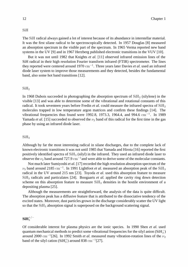
coupled radio frequency (rf) discharge. Several research groups around the world use thesedischarges to study silane discharges. One of the groups that has been studying the nucleationand growth of particles in silane discharges is the ’Group de Recherche sur l’Energetique desMilieux Ionises’ (GREMI) in Orleans [46]. In recent years, there has been a close collaborationbetween this group and the group EPG in Eindhoven, and since it would be very useful touse their scientific results as a starting point for the research in Eindhoven, the design of thenew discharge configuration will be based on the setup in Orleans. The setup from Orleans isdescribed in detail in [47]. A general view is given in Fig.2.4, and the main characteristics aregiven below:
vacuum vessel
stainless-steelbellows
gas and rf
oven
plasma chamber
pumping
windows
133 mm
33 mm
Fig. 2.4: Schematic view of the experimental setup in Orleans.
• The powered electrode consists of a stainless-steel grid, 130 mm in diameter, that alsoserves as gas inlet.
• The grounded electrode is formed by a stainless-steel cylindrical box, with a diameter of133 mm. The bottom of this box is formed by a stainless-steel grid, that serves as the gasoutlet of the discharge volume. The holes in the grid have a diameter of 1 mm and thetransparency of the grid is 20 % .
• The distance between the electrodes is 33 mm. The combination of the shower head topelectrode and the grid bottom allows for a homogeneous laminar flow.
• Three vertical slits in the side wall of the cylindrical box allow optical access to thedischarge volume.
• The complete discharge chamber can be translated vertically for spatially resolved mea-surements.

28 Chapter 2
• The discharge chamber is placed in a cylindrical oven, with an inner diameter of 146 mmand a height of 250 mm, to control the wall temperature.
• The complete structure of oven and plasma chamber is placed in an aluminum vacuumvessel.
Spatially resolved measurements
In chemically active discharges like silane discharges, spatially resolved measurements giveinvaluable extra dimensions to the experimental data. Since the stability of the ring down cavityis a very critical item in the complete design of the setup, the most logical way to performspatially resolved measurements is to keep the cavity fixed and move the discharge through theoptical beam, like in the setup of Orleans. To obtain 2-dimensional density profiles, the systemwith the bellow has to be extended to enable, next to vertical scans, also horizontal scans.
2.5 Data Acquisition
With the old IRLAS measurements time scales typically varied from some tens of millisecondsto many seconds. The use of lock-in amplifiers made this technique very time uncritical. Cavityring down measurements on the other hand, take only tens of microseconds, and the sensitivityof this technique is determined by the smallest detectable change in this ring down time, whichmakes this technique very time critical. The old data acquisition system used for the IRLASmeasurements is not able to handle the time resolution necessary for cavity ring down measure-ments. It was therefore necessary to obtain a new data acquisition system. The general demandson the new data acquisition system were:
• The analog digital converter (ADC) needs to be fast enough to record a ring down tran-sient. Five to ten data points per ring down time is sufficient for a good exponential fit.With an expected ring down time of ca. 1 µs , this leads to an sampling rate of at least10 MHz. Very important is the control of the jitter on the time base, since this is directlycoupled to the noise in the ring down time.
• Another demand on the data acquisition system is the resolution of the ADC. The reso-lution of the digitized ring down transient determines the smallest detectable change inring down time, and thereby the detection limit of the new diagnostic. Therefore the ADCshould be at least 10-bits deep, but 12-bits is preferable.
• In order to increase the signal to noise ratio, several ring down transients can be averaged.The use of pulsed lasers for CRDS experiments limits the repetition rate of the ring downtransients to the pulse rate of the laser. When a CW laser is used, no such limits exist and,theoretically, the repetition rate is only limited by the time needed to fill the cavity withphotons and the ring down time. This can lead to theoretical repetition rates of tens ofthousands of ring downs per second. In practice however, some time is needed to modematch the cavity to the laser, but ring down rates of several thousands per second arefeasible. The exponential nature of the ring down signal allows to simply add several ringdown transients before fitting to an exponential. With ring down rates of several thousandsper second, it is not possible to send the data of each transient separately. Therefore it

Design considerations 29
is necessary that the data acquisition unit has a sufficiently large on board memory. Theaddition of one thousand 12-bit signals necessitates a 22-bit deep memory.
• The unpredictable overlap of the laser mode and the cavity mode determines the signallevel in the cavity, and thereby the moment that the laser should be detuned to start thering down transient. A fourth demand on the data acquisition system is therefore a flexi-ble triggering system, with an analog input and several outputs with different time delays.One trigger signal should start the ADC, and another trigger signal should start the detun-ing of the laser. The time delays should be tunable in the order of tens of nanoseconds
2.6 The ring down cavity
The use of an infrared tunable laser diode for cavity ring down spectroscopy leads to constraintson the design of the ring down setup not known in the field of cavity ring down spectroscopy sofar. Those problems arise from the wavelength region under consideration, the expected outputpower and line width of the laser. It is therefore eminent to first look into the theory of opticalcavities 1.
High finesse optical cavities
In general, open optical cavities are composed of a number of reflecting surfaces that are alignedsuch that light waves can bounce up and down the cavity. At each reflecting surface the shapeand amplitude of the light waves will be changed because of diffraction and other losses. Forsome light waves the losses are so high that after a few round trips the light wave is effec-tively extinguished. For other light waves the shape of the wave front converges to a stationarydistribution, called a mode of the optical cavity.
The simplest optical cavity is composed of two plane mirrors. The mode configurationof such a simple cavity can be obtained by an iterative approach using the Kirchhoff-Fresneldiffraction theory. In this method, the square plane mirrors are replaced by an equivalent ar-rangement of an infinite number of apertures with the same size as the mirrors. The amplitudedistribution A(x, y) of a plane wave traveling through the apertures in the z direction is alteredby diffraction at each aperture, and the amplitude distribution at one aperture An(x, y) can becalculated from the distribution at the previous aperture An−1(x, y) with the paraxial approachof Kirchhoff’s diffraction theory:
An(x, y) = −i
2λ
∫ ∫An−1(x
′, y′)1
ρe−ikρ (1 + cos θ) dx′ dy′, (2.1)
with k the wave vector of the light wave propagating in the z-direction. The denotation of Θand ρ is depicted in Fig. 2.5
A stationary field distribution is obtained when the shape of the wave front at a certainaperture is identical to the shape of the wave front at the previous aperture [42].
The resulting integral equation can not be solved exactly, but for the case of a large distancebetween the mirrors compared to the size of the mirrors it has been shown that stationary fielddistributions do exist. Boyd and Kogelnik generalized the computations to confocal cavitieswith curved mirrors [43]. For the case that the size of the mirrors is much smaller than the
1The following section is based on Demtroder’s Laser Spectroscopy [42]

30 Chapter 2
A (x’,y’)n 1
A (x,y)n
n-1 n
d
X
Y Z
Fig. 2.5: Illustration of Eq. (2.1). ρ is the length of the vector from the point A(x’,y’) in theplane n− 1 to the point A(x’y’) in the plane n , cosΘ = ρ/d.
distance between the mirrors, the two-dimensional equation can be decomposed into two one-dimensional equations which can be solved analytically. The resulting stationary amplitudedistribution in a plane z perpendicular to the cavity axis is given by:
Am,n(x, y, z) = C Hm(X) Hn(Y ) e−(X2+Y 2) e−iφ, (2.2)
with z the axial postion measured from the center of the cavity and x and y the two coordinatesperpendicular to the cavity axis. C is a function of z,m, and n. Hm is the Hermitian polynomialof the mth order. X is a function of x and z, Y is a function of y and z, and w =
√x2 + y2
is the distance to the cavity axis ([42] Eq. 5.25). The last factor of Eq. (2.2) is the phase factorwhere φ is given by:
φ(w, z) = k
[r
2(1 + ε2) +
w2
r
ε
1 + ε2
]+ (1 +m+ n)
π
2− arctan
1− ε1 + ε
, (2.3)
with ε = 2zr
the relative z-coordinate, and k = 2πλ
= 2πνc
.The stationary field distributions of confocal cavities turn out to have an eigen frequency
spectrum which can be directly derived from the condition that the phase fronts at the mirrorsurfaces have to be identical to the shape of the mirror surfaces themselves. Because thesestationary fields represent standing waves, the mirror separation d equals an integer multipleof λ/2. For confocal cavities (d = r) substitution of φ = qπ into Eq. (2.3), with q an integercalled the longitudinal mode index which represents the number of half waves that fits insidethe cavity, and z = r/2, results in eigen frequencies given by:
ν =c
2d
[q +
1
2(m+ n + 1)
], (2.4)
with m and n the transverse mode indices. Modes with m = n = 0 are called axial or funda-mental modes and modes withm > 0 and/or n > 0 are the higher order transverse modes. Theaxial modes closes on itself after one round trip and the intensity distribution in a plane per-pendicular to the propagation direction has a Gaussian profile with an 1/e half width ws givenby:

Design considerations 31
ws =
√√√√λd2π
(1 + 4
z2
d2
), (2.5)
with d the distance between the mirrors, λ the wavelength of the light inside the cavity, and zthe distance from the center of the cavity. From Eq. (2.5) it directly follows that the mode hasthe smallest radius in the center at z = 0. For a typical wavelength of 5 µm and a cavity lengthof 1 m, the resulting beam waist (= 2w) is 1.8 mm. The beam diameter on the mirror (z = d/2)is√2 times the beam waist, which for the example above results in a spot size of 2.5 mm.
Higher order modes need several round trips before the wave closes on itself (Fig. 2.6) andthe resulting intensity distribution is not Gaussian, but has several maxima. m and n representthe number of nodes in the cross section of the intensity distribution of these modes (Fig. 2.7).Since the intensity distribution of higher order modes is lying further from the axis, the diffrac-tion losses of these modes are higher. Therefore, the relative intensity of higher order modes islower than of the axial mode.
Fig. 2.6: Schematic view of the TEM00 and the TEM01 transverse mode.
Fig. 2.7: Intensity distributions of different transverse modes measured with a CCD camerabehind the exit mirror of a high finesse optical cavity. Top-left = TEM00; Top-right =TEM01; Bottom-left = TEM02; Bottom-right = TEM04. (Courtesy of the group AQT.)
32 Chapter 2
From Eq. (2.4) it follows that the eigen frequency spectrum of the confocal cavity is degen-erate because the transverse mode with q = c1 and m + n = c2 has the same frequency as thetransverse modes with q = c1 + p and m + n = c2 − 2p. The distance between two adjacentaxial modes is ∆ν = c/2d , but the modes with m + n = odd lie exactly halfway these axialmodes and the free spectral range (FSR) of a confocal cavity is therefore:
∆νconfocal =c
4d. (2.6)
If the mirror separation d is slightly different from the radius of curvature of the mirrors rthe degeneracy is removed and the eigen frequencies are given by:
ν =c
2d
[q +
1
2(m+ n + 1)
(1 +
4
πarctan
d− rd+ r
)], (2.7)
One very important property of an optical cavity is its finesse, which is defined as the ratioof the free spectral range and the line width of a cavity mode δν:
F =FSR
δν. (2.8)
For a perfectly aligned optical cavity consisting of two plane mirrors, diffraction losses limit thefinesse to ca. 50. But, since spherical mirrors tend to refocus the diffracted light back into thecavity, the diffraction losses for a confocal Fabry-Perot cavity are much lower. Furthermore,spherical mirrors can be polished to a higher precision than plane mirrors, which makes thatthe total losses caused by e.g. the surface roughness of the substrates and inhomogeneity of thereflecting layers are only slightly higher than the reflectivity losses. For a confocal Fabry-Perotcavity used in the visible part of the spectrum a finesse of ca. 300 can be achieved with mirrorswith a reflectivity of 0.99.
For the mid-infrared, where wavelengths are typically one order higher than in the visible,the losses caused by the surface roughness of the substrate, which is taken relative to the usedwavelength, are one order lower. The losses caused by inhomogeneities in the reflecting layers,which are a quarter of a wavelength thick, are also one order lower. This makes that the totalfinesse of a confocal cavity is almost completely determined by the reflectivity of the mirrors,and the total finesse F is identical to the reflectivity finesse FR:
F = FR =π√R
1−R =FSR
δν. (2.9)
Reflectivities of 0.997 can be obtained with multi-layer coatings quite easily, which leads to afinesse of more than 1000. Combination of Eq. (2.6) and Eq. (2.9) leads to a formula for thehalf width of a cavity mode δν:
δν =c
4πd
1− R√R
(2.10)
A confocal cavity constructed from two spherical mirrors with a reflectivity R of 0.997 at adistance d of 1 m thus has a FSR of 75 MHz, a finesse of ca. 1000, and a mode width of ca. 140kHz.

Design considerations 33
Coupling the diode laser to a cavity
Eq. 2.7 gives the theoretical possibilities to have a stable light wave inside the cavity. If the linewidth of the laser used to excite the cavity is broader than the distance between two adjacentmodes, several modes will be excited simultaneously. This leads to mode beating inside thecavity, which generates unwanted oscillations in the ring down transients. To avoid the problemof mode beating, some measures have to be taken.
First of all, the optical cavity can be designed in such a way that the mode spacing is opti-mized. The frequency spacing between two adjacent higher order transverse modes is usuallymuch smaller than the mode spacing between different fundamental modes. So, to avoid thesimultaneous excitation of different cavity modes, the transverse mode spacing should be max-imized. From Eq. 2.7 it follows that the widest mode structure is achieved when the radii ofcurvature of the mirrors (r) equal the distance between the mirrors (d). The cavity thus con-structed is a confocal cavity, since the focal length of a spherical mirror equals r/2. The modespacing for such a cavity is given by Eq. (2.6).
The expected laser line width of ca. 30 MHz gives a maximum for the cavity length ofc/4 × 30 · 106 = 2.5 m. To ensure an efficient coupling of such a cavity to a laser, either thelaser wavelength has to be matched to the cavity or vice versa.
The second solution to mode beating makes use of the distinct optical paths of the differenttransverse modes. Since the different modes follow different optical paths, they use differentparts of the mirrors. By illuminating a particular part of the entrance mirror, it is possible toexcite a specific transverse mode. The use of mode matching optics makes the mode selectionmore specific. The simplest mode matching optics consists of a diaphragm or a pin hole. A sim-ple positive lens with a long focal distance can be used to enhance the effect of the diaphragm.The concept of matching the confocal cavity to the laser or vice versa automatically gives ahandle to the active coupling and uncoupling necessary to ’chop’ the laser.
Another issue that plays an important role during the incoupling of the laser light into thecavity is the lens working of the entrance mirror. A three millimeter thick slab of zinc-selenide,with one flat side and one concave side with a radius of curvature of one meter works as anegative lens with a focal lenght of ca. -72 cm. This means that an incoming parallel laser beamwill be divergent after passing the mirror. Since a divergent beam inside the cavity will notlead to a stable cavity mode, the divergence has to be prevented. This can be done by placing apositive lens with a long focal distance in front of the cavity. The distance between the positivelens and the entrance mirror should be such, that the system of the two lenses has an effectivefocal point either at infinity, or exactly in the center of the cavity.
Further constraints on the cavity
Other constraints on the design are given by the fact that the diagnostic will be used on realdepositing discharges. The mirrors used to construct the cavity are very sensitive for contami-nation and must therefore be protected from the silane plasma. The first step in protecting themirrors from the discharge is to keep them as far away from the discharge as possible. Thisconflicts directly with the demands for a large mode spacing and so some concessions have tobe made.
The concept of the confocal cavity will only work if the cavity is stable during the build upand the ring down of the light intensity in the cavity. This implies that the distance between andthe alignment of the mirrors must be stable within the limits of the cavity line width for several

34 Chapter 2
hundreds of microseconds. On the other hand, the discharge itself is also very sensitive for anydisturbances from outside, so the optical cavity and the discharge chamber must be constructedin such a way that they have no influence on each other. This is made even more difficult by thedemand of spatially resolved measurements in two directions.
2.7 The mirrors
The general demands on mirrors for cavity ring down spectroscopy are a high reflectivity (>0.99) and a finite transmission (≈ 1 - R). For normal mirror coatings, like gold or aluminum,these two demands cannot be satisfied simultaneously. Only very thin layers of e.g. gold havea finite transmission, but for these thin layers the reflectivity is limited to ca. 95 %. Higherreflectivities can only be obtained with thick layers, which absorb all the light they do notreflect, thereby nullifying the transmission.
The only way to fulfill both demands is with the use of multi-layer coatings. They consistof a stack of layers of dielectric materials with alternately high and low refractive indices, on atransparent substrate. The optical thickness of each layer is a quarter of the wavelength to bereflected. Therefore each mirror only reflects a specific and small part of the electromagneticspectrum.
Reflectivities that can be obtained with these multi-layer coatings are 99.9999 % and higher.The effective reflectivity for such layers is largely determined by the surface roughness of theused substrate, and the quality of the layers.
The past decade mirrors of this kind have been produced for the complete spectrum fromca. 215 nm up to 3.3 µm. For no obvious reason, but most probably due to the absence of asuitable light source to perform ring down measurements, they have never been produced forwavelengths beyond 3.3 µm. Since the success of the complete setup stands or falls with themirrors, the first objective will be to obtain mirrors with the proper reflectivity between 4.2 and5.6 µm (≈ 1800 - 2400 cm−1).

Design considerations 35
2.8 Summary and time schedule
Summary
The accomplishment of the new setup covers many different aspects. Some parts are routinejobs but most parts are completely new and highly innovative. As most work will be doneby different groups within the university and all these groups depend on each other concern-ing essential information, a reliable project management is required. Before all the differentsubprojects are put in a time schedule, a summary is given in table 2.1.
Table 2.1: Overview of the planned activities to come to the realization of the mid-infraredcavity ring down spectrometer.
Item DescriptionLaser current source Modification to allow for very short pulses superimposed
on the DC currentLaser control and Design, realization and testing of all the modules neededdata acquisition to control the laser and acquire and pre-process the dataOpical feedback Design, realization and testing of an optical setup to
prevent laser light from re-entering the laser diodeOptical cavity Design and realization of a mechanically and optically
stable cavityObtaining the mirrors for the cavityDesign and realization of a method to control the cavitylength
Vacuum vessel Design and realization of the main vessel around the ringdown cavityRe-design and realization of the additional parts of thevacuum vesselUpgrading the PLC to control the pumps and gas system
Discharge Define the external parameters if the dischargeDesign and realization of the modular discharge chamberDesign and realization of the 2-D manipulator includingcontrol software and hardware
Time schedule
As a basis for this project management, a time schedule is made (Fig. 2.8). The time schedulestarts with the quotation for the mirrors and from there links all the different parts together toarrive at a fully operational setup in the beginning of 1999.

36 Chapter 2
Item
Laser
curr
entsourc
e
Laser
contr
oland
data
acquis
itio
n
Opticalfe
edback
Opticalcavity
Vacuum
vessel
PLC
Dis
charg
e
Task
Modify
curr
entsourc
eO
bta
inpuls
egenera
tor
Build
and
test
Definitio
nand
desig
nm
odule
sTestand
imple
mentm
odule
sW
rite
necessary
softw
are
Obta
inquart
er
wave
pla
teTestprincip
lew
ith
CO
laser
Desig
nopticalcavity
Constr
uctcavity
Getquota
tion
on
mirro
rsO
rder
mirro
rsD
esig
ncavity
modula
tion
Constr
uctcavity
modula
tion
Desig
nm
ain
vessel
Constr
uctm
ain
vessel
Redesig
nadditio
nalpart
sC
onstr
uctadditio
nalpart
s
Upgra
de
PLC
Desig
ndis
charg
echam
ber
Constr
uctdis
charg
echam
ber
Desig
nm
anip
ula
tor
Constr
uctm
anip
ula
tor
Jan.9
8F
eb.9
8M
ar.98
Apr.98
May.
98
Jun.9
8Jul.98
Aug.9
8S
ep.9
8O
ct.98
Nov.
98
Dec.9
8Jan.9
9
Pers
onalta
sk
Support
gro
up
within
univ
ers
ity
Third
part
youts
ide
univ
ers
ity
Sum
mary
Fig. 2.8: Time schedule of design and realization of the complete cavity ring down setup.

3The mid-infraredcavity ring downspectrometer

38 Chapter 3
3.1 Introduction
The design considerations of chapter 2 gave an overview of the know-how at the start of theproject. With this knowledge the different support groups started their work and quickly startedto develop new insights. These new insights were distributed to all the persons who neededspecific information. This led to the realization of a complete setup in accordance with thedemands as they were known at the end of the realization phase.
This chapter gives an technical overview of the realized setup. A description is given ofall the different parts and explanations will be given about specific choices made during thedesign and fabrication phases. At the end of this chapter it will be clear that, since the detectoris directly coupled to the laser current control unit, there is literally no beginning or end to thissetup. The chapter therefore begins with that part of the setup that can be considered to be thecentral part of any cavity ring down setup: the ring down cavity.
3.2 The ring down cavity
3.2.1 The body of the cavity
The optical cavity is essentially comprised of an aluminum pipe with vibrational eigen fre-quencies far away from the vibrational frequencies of the pumps (Fig. 3.1). The vibrationalfrequencies of the pumps were determined to have strong maxima between 700 and 800 Hz,while the first dominant eigen frequency of the cavity lies at 1200 Hz. The material, size andwall thickness all contribute to the fact that the higher order modes need considerable energiesto get excited. In order to avoid external vibrations from e.g. the ground floor to be transmittedto the cavity, the cavity is suspended in the vacuum vessel by two sets of springs to carry theweight and rubber flaps to damp all the vibrations that might get to the vacuum vessel (Fig. 3.2).The only vibrations that could get into the system were vibrations that were acousticly coupledto the cavity while the vacuum vessel was still under atmospheric pressure. This gives an easilyrecognizable broadening of the cavity modes that immediately vanishes when the pumps areturned on and the vessel is evacuated.
The cavity has an inner diameter of 35 cm and a central aperture in the top to allow adischarge to be put in and moved around through the optical path. The optical path is setsomewhat off-axis. The reason for this is that many discharges are rotationally symmetric andduring spatially resolved measurements one only needs to scan one side of the discharge.
To allow other diagnostics to be used on the same discharge simultaneously, the cavity isequipped with a number of apertures. Two large apertures perpendicular to the optical pathand four apertures under an angle of 45 degrees that are all centered on the same point of theoptical path. Another set of two apertures under an angle of 72.5 degrees with the vertical axisprovides an easy way to perform ellipsometry measurements. Electrical or other connectionscan be made through 6 apertures set at both ends of the cavity, but the two most importantopenings are of course the apertures for the cavity ring down experiment.

The mid-infrared cavity ring down spectrometer 39
Top view
Side viewEnd viewCross-section
o: optical portv: versatile portp: pump portd: discharge porte: ellipsometry portc: cavity ring down porto
o
o
o
o
v
v
v
pp
p
dd
e
ee
e
e
c
c
c
c
c
Fig. 3.1: Cross-sections of the optical cavity.
Fig. 3.2: Side and front view of the optical cavity, suspended in the open vacuum vessel.
3.2.2 The mirror mounts
The mirror mounts consist of two parts for each mirror. To match the cavity length to thelaser wavelength one of the mirrors is mounted on a commercially available piezo-electric tip-tilt translator (Physics Instrumente (PI) S-315.10 Piezoelectric Tip-Tilt translator, from now oncalled piezo (Fig. 3.3)), with accompanying three channel amplifier for low voltage piezoelectrictranslators (PI E-663.00). A 10 mm diameter aperture through the center of the translator allowsoptical beams to pass the piezo. The piezo can translate the mirror over 12 µm and tilt the mirrorwith a maximum angle of 600 µrad. It is made from low voltage piezo crystals, so it reaches its

40 Chapter 3
maximum translation or angle at an applied voltage of 100 V. For symmetry purposes, the othermirror is mounted on a a dummy translator with identical dimensions, but without the piezofunctionality inside.
10
20Piezostack
Fig. 3.3: The piezo package. The length of the cavity can be scanned by applying a voltageto all three piezo stacks simultaneously. By applying a voltage to one of the piezo stacksthe mirror can be tilted.
The piezo and the dummy are mounted in the second stage of the total mirror mount. Thispart provides a way to accurately align the mirrors by sophisticated 2-D hinges (Fig. 3.4). Italso houses the means to protect the mirrors from the discharge (Fig. 3.5). The central part ofthe mirror mount is equipped with baffles over a length of ca. 15 cm, to decrease the chance ofradicals to reach the mirrors. Next to this an extra gas flow can be injected at the position of themirrors to flush the mirrors continuously with e.g. argon.
Piezo + mirror
Spindle
Hinge
Fig. 3.4: Schematic view on the hinge designed to align the mirror. By turning the spindle,which is equipped with two slightly different threads, the part of the mirror mount holdingthe piezo and the mirror can be aligned. A second hinge perpendicular to the hinge shownin the figure enables the mirror to be aligned in the other direction.

The mid-infrared cavity ring down spectrometer 41
Purge gas
Mirror
Piezo
Fig. 3.5: Schematic view on the cental part of the mirror mount designed to protect themirrors from the discharge.
3.2.3 The mirrors
The mirrors for the CRDS setup were obtained from II-VI inc. The substrate is a round piece ofzinc-selenide (ZnSe), 3 mm thick, with a diameter of 25 mm. One side of the substrate is flat,and the other side is concave, with a radius of curvature of 1 meter. The flat side has an anti-reflection coating, and the spherical side bears the multi-layer coating. The reflectivity is higherthan 0.996 for the complete wavelength range from 4.2 to 5.6 µm (Fig. 3.6). To avoid multiplereflections at the backside of the mirror, the flat side stays under an angle of ca. 3 degrees withthe optical path.
4,0 4,5 5,0 5,5 6,00,970
0,975
0,980
0,985
0,990
0,995
1,000
Ref
lect
ivity
Wavelength ( mm)
Fig. 3.6: Spectral reflectivity of the mirrors.

42 Chapter 3
1800 2000 2200 24000,0
5,0x10⁻⁷
1,0x10⁻⁶
1,5x10⁻⁶
2,0x10⁻⁶
2,5x10⁻⁶
Rin
g do
wn
time
(s)
Wave number (cm-1)
Fig. 3.7: Corresponding ring down time for a 1 meter cavity.
3.3 The vacuum system
3.3.1 The vacuum vessel
The vessel consists of four parts. The central part is a horizontally orientated stainless-steelcylinder, 80 cm long with an inner diameter of 45 cm. This part accommodates and supportsthe ring down cavity, and is equipped with the apertures for the discharge and the pumps, theapertures for the optical windows and the electrical or other connections. It is sealed with twoshells that contain the ring down windows and the ellipsometry windows.
Fig. 3.8: Side and front view on the closed vacuum vessel.
The aperture in the bottom of the central cylinder is connected to the slightly adapted lowerpart of the original vacuum vessel of the old silane setup. Besides the 160 mm flange in the top,used to connect it to the main vessel, are two other 160 mm flanges and six 40 mm flanges. Oneof the 160 mm flanges goes directly to the turbo molecular pump, and the other one is a spare

The mid-infrared cavity ring down spectrometer 43
flange. Two of the 40 mm flanges are used for a bypass line to the turbo and roughing pumps,the other four have versatile functions (e.g. pressure gauges).
o: optical portv: versatile portp: pump portd: discharge porte: ellipsometry portc: cavity ring down port
c c
e
e
o
o
o
p
d
v
v
v
v
c
p
p
d
v
oo
Fig. 3.9: Cross-sections of the new vacuum vessel.
Fig. 3.10: Cross-sections of the total setup, mounted on its frame.

44 Chapter 3
3.3.2 The pumps
The pumping system consists of three pumps: a double stage rotary pump (Leybold TrivacD65BCS), a roots blower (Leybold Ruvac WS251), and a turbo molecular pump (Leybold Tur-bovac 450). The roughing pumps can pump the vessel directly, via a bypass, to a fore-pressureof ca. 10−2 mbar. At this pressure the bypass has to be shut and the turbo molecular pumpbrings the pressure to 10−6 mbar or lower. The turbo pump can either pump the vessel directlyvia the 160 mm flange, or via a bypass. The last option is used when large amounts of dustparticles are produced in the discharge. The bypass is then used to catch the dust particles asmuch as possible and prevent them from reaching the pumps.
3.3.3 Gas supply
Three gas lines with three different mass-flow controllers end, via a manifold, in one gas linethat leads to the vacuum vessel. Each single gas line can be closed by a pneumatic valve, as canthe main line.
3.3.4 The PLC
The programmable logic controller (PLC) guards the setup and protects the equipment andpersonnel for unsafe situations. Starting at the rotary pump, each pump or valve in the setupcan only be operated when all parts that come before it, satisfy certain safety rules. The mainsafety rules are as follows:
• The rotary pump can be turned on when all the three phases of the 380 V power supplyare present.
• If the rotary pump is running and has reached a sufficiently low pressure in between therotary pump and the roots blower, the roots blower can be switched on. Also, when therotary pump is running, the bypass from the roughing pumps to the vacuum vessel canbe opened. This valve will be closed automatically, or refuse to open, when the pressureinside the vessel is below 5 · 10−2 mbar.
• If the pressure after the roots blower reaches 10−1 mbar, and the water cooling of the turbopump is running, the turbo pump can be turned on. When the turbo pump is acceleratingor running, the main valve between the turbo pump and the vacuum vessel can be opened.This will automatically close the valve to the bypass. If the turbo pump does not reach itsfinal speed within 10 minutes, the main valve is closed and the turbo pump is shut down.
• When the turbo pump has reached its final speed, the gas supply lines and the plasmachamber can be operated.
• In case of an emergency, e.g. a major vacuum breakdown or a manual alarm, all valves inthe gas supply and all valves to the pumps are closed and the pumps are turned off.

The mid-infrared cavity ring down spectrometer 45
Rotary vane pump
Roots pump
Turbomolecularpump
Piranipressuregauge
Penningpressuregauge
Baratronpressuregauge
Exhaust
Throttlevalve
Mass flowcontrollers(100 sccm)
Mass flowcontroller(5 sccm)
Gas 3
5 % Silane95 % Argon
Argon
Mirror purge line
By-pass / dust trap
Discharge chamber
Vacuum vessel
gas cabinet
Fig. 3.11: Pump and gas supply diagram.
3.4 The discharge
The discharge chamber
The design of the discharge chamber is based on the ”plasma box” approach introduced byBouchoule and Boufendi in Orleans. It has a shower head type powered electrode in a groundedcylindrical chamber, or so called pill box, 14 cm in diameter. The diameter of the poweredelectrode is 13.5 cm. The bottom of the grounded housing is made of a grid, to establish a welldefined laminar flow through the whole plasma region. The side wall of the plasma box is a 40mm high cylinder, with a wall thickness of 5 mm.
The plasma box is modular in design, and the bottom grid and the side wall can easily bereplaced to adapt the plasma chamber for other experiments, e.g. probe measurements. By mak-ing suitable apertures in the side wall, optical beams can be scanned horizontally or verticallythrough the complete plasma region.
The top part of the grounded housing is thermostrated by a closed cycle water heating sys-tem. Due to the wall thickness and material, the complete chamber will obtain a homogeneoustemperature, that can be set anywhere between 10 and 95 oC. A thermocouple connected to thegrounded housing controls the temperature.

46 Chapter 3
Plasma region
Gas inlet
Water coolingRF connection
Bottom grid
Shower head typepowered electrode
Groundedhousing
140 mm
40 mm
Fig. 3.12: Cross-section of the modular discharge chamber.
3.4.1 The manipulator
Since the alignment of the optical beam of the CRDS experiment is very critical, spatiallyresolved measurements have to be performed by scanning the discharge through the opticalbeam. Therefore, the plasma chamber is mounted on a 2-D manipulator. The manipulator ismoved by two DC motors outside the vacuum vessel, which scan the plasma over the completevertical extent of the discharge, and, because of the rotational symmetry, over half the diameterof the discharge. The scanning resolution is 0.05 mm vertically, and 0.1 mm horizontally.
Scanning the discharge gives line-of-sight-integrated 2-D spatially resolved lateral measure-ments, that can be converted into radial profiles by Abel inversion.
Fig. 3.13: (left) The plasma box underneath the manipulator; (right) Close-up of the plasmabox. (Pictures taken before the apertures were made in the side wall)

The mid-infrared cavity ring down spectrometer 47
3.5 The diode laser system
3.5.1 Basic principles of semiconductor diode lasers
As the name already suggests, semiconductor diode lasers are made of semiconductors, andhave the electrical characteristics of diodes. A diode consists of two layers of semiconductormaterial. One of the layers is doped with acceptor impurities (holes), or p-doped, and the otherlayer is doped with donor impurities, or n-doped. At the interface of the two layers, called thep-n-junction, the majority carriers from one layer diffuse into the other layer. This diffusioncauses the p-doped material to become negatively charged and the n-doped layer to becomepositively charged. This effectively stops further diffusion, and so a depletion layer is formed.
If a current is injected via two electrodes, extra recombination sites are generated in thedepletion zone. The energy from the recombination processes can be released either as heat oras light, with the latter option giving rise to the name Light Emitting Diode (LED).
Two extra features are needed to turn a LED into a laser diode: population inversion and aresonant cavity [48]. The population inversion is created by an excess in the injected current.The cavity is formed by the polished or cleaved end facets of the crystal. Typical cavity lengthsof a laser diode are several hundreds of micrometers. The photons that bounce up and down thecavity stimulate the recombination sites to release their energy by emitting photons, before theenergy is dissipated as heat.
Vertical confinement is obtained by the use of double heterostructures, around an undoped,or intrinsic layer. The intrinsic layer, which acts as the recombination zone, is sandwichedbetween a p-doped structure and an n-doped structure, that both consist of two identically dopedmaterials with different refractive indices. The change in refractive index effectively confinesthe photons vertically.
Two methods exist to confine the photons in the horizontal plane, perpendicular to the op-tical path: index guiding and gain guiding. With index guiding, the active zone is limitedhorizontally by two regions with another refractive index, just like the vertical confinement.Gain guiding is obtained by limiting the horizontal extent of the injection current, end therebylimiting the region of population inversion (Fig. 3.14). In both ways, laser action can be limitedto a narrow stripe, several µm broad, less than a µm thick, and ca. 250 µm long.
electrodes
n-doped substrate
High-resistance material
intrinsic layer
n-doped confinement layer
p-doped confinement layer
recombination zone
heterojunction 1
heterojunction 2
current
p-doped material
Fig. 3.14: End view of a gain guided stripe laser diode.

48 Chapter 3
Lead salt laser diodes
Laser diodes that emit light in the visible or near infrared are made of compounds of elementswith 3 and 5 valence electrons (e.g. Ga, As, In, etc.), the so called III-V semiconductors. Tocreate laser diodes that emit longer wavelengths, materials are needed with a much smaller bandgap. These materials are composed of three (ternary) or four (quarternary) elements with 2 and6 valence electrons (e.g. Pb, Sn, Se, etc.)[49]. The combination of valence states II and VI leadsto bonds somewhat more ionic than in III-V compounds, and gives these materials a salt-likecrystalline structure. Since most of those compounds contain the element lead, they are calledlead salt laser diodes.
Laser diodes based on PbEuSeTe emit light in the range from 3.3 to 6 µm . Diodes madefrom PbSSe cover the range from 4.2 to 8 µm , and the PbSnTe and PbSeSn compounds extendthe range up to 30 µm . To reduce the blackbody emission in the laser wavelength band, leadsalt laser diodes are operated at cryogenic temperatures.
The center wavelength of a diode is determined by the exact combination of materials. But,the temperature and the driving current control the cavity length and the refractive index of thelaser channel, and by changing this refractive index and the temperature, the wavelength can betuned over ca. 200 cm−1.
In practice, tuning is complicated by hopping between different modes. The modes aretypically one to three wavenumbers long, and lie several wavenumbers apart. Each individualmode is ca. 0.0003 cm−1, or 10 MHz wide (Fig. 2.2).
Beam characteristics
The emitting area of a diode is wider than it is high, and both dimensions are in the order of,or smaller than the wavelength of the emitted light (Fig. 3.14). Therefore, the diode produces arapidly diverging beam, with divergences that can be 50 degrees or more. Since the height of theactive region of the diode is smaller than the width, the divergence in the plane perpendicularto the active layer will be larger than the divergence parallel to the active layer. The resultingbeam is therefore not only very divergent, it is also astigmatic.
3.5.2 The helium cooled diode laser system
The helium cooled diode laser system is purchased as a complete system, consisting of theLaser Photonics L5800 laser source assembly, a monochomator, a sample cell, an etalon, severaldetectors and accompanying optics. The laser source assembly itself contains the laser modules,cooling equipment, temperature stabilizer and current source.
The cooling equipment and temperature stabilizer
To reach the necessary cryogenic temperatures, the laser diodes are contained in a closed-cyclehelium refrigerator (Laser Photonics L5731). The laser diodes itself consists of a properlydoped, single crystal, lead salt chip, several hundreds of micrometers long and wide, mountedin a gold-plated copper package. This copper package is ca. 20 mm long, 6 mm broad and 5mm high, and functions as the heat sink for the diode. The refrigerator can hold up to four ofthose packages.
The refrigerator is capable of maintaining temperatures down to 10 K, with a stability betterthan 3 · 10−4 K over the complete operating range from 20 to 60 K. This stability is obtained

The mid-infrared cavity ring down spectrometer 49
by the use of the Laser Photonics L5720 Cryogenic Temperature Stabilizer, which uses twosilicon diode sensors and a heater. The required temperature can be set with the coarse and finetemperature controls on the front panel of the L5720, or via a BNC connector on the back of theunit. Another BNC connector can be used to measure the deviation between the setpoint andthe actual temperature.
The current source
The current through the diode is provided by the Laser Photonics L5820 Laser Control Module.This is a highly stable current supply, that incorporates a variety of protection features andsweep and modulation options for operating tunable diode lasers. The laser current can be setwith the coarse and fine current controls on the front panel, or via a BNC connector on the frontpanel of the laser control module. The current changes 20 mA per applied volt, and the appliedvoltage may be varied between -10 and +10 volts. To resolve a rovibrational absorption line itis necessary to take current steps in the order of 10−5 A.
The collimating optics
In order to turn the diverging beam coming out of the diode into a more parallel beam that canbe transported over longer distances, a collimating lens or mirror has to be used. Therefore,the L5800 laser source assembly is equipped with an off-axis parabolic mirror (OAP mirror).This OAP mirror has a focal length of 20 mm and is equipped with three micrometer screws forprecise positioning in all three translational directions.
The monochromator
To select one of the modes coming out of the diode, a monochromator (Laser Photonics L5151)is positioned directly after the refrigerator and the OAP mirror. Inside the monochromator,the multimode beam is sent through a 400 Hz mechanical chopper. Subsequently, the beam isexpanded and projected on a blazed grating. After the grating, the beam is compressed again,and sent through a 1 mm slit, to select one of the modes. The grating is controlled by the gratingcontrol unit. This unit can be controlled manually or via the RS-232 interface.
3.6 The detection branch
The detector
In principle, there are two basic types of infrared detectors: thermal detectors and photon de-tectors. In thermal detectors, the absorption of radiant energy causes a raise in temperature ofthe detector, and thereby a change in its electrical properties. The response of these detectorsis slow and the detectivity is several orders lower than that of photon detectors, which makesthem unsuitable for CRDS experiments.
In photon detectors, incident photons interact directly with the electrons in the detector ma-terial, which makes them very fast and very sensitive. The response of a photon detector isheavily wavelength dependent. The upper limit of the detectable wavelength range is definedby the band gap of the detector material. The most commonly used materials are ternary semi-conductor compounds of mercury, cadmium and telluride (MCT or HgCdTe), for which the

50 Chapter 3
band gap can be chosen between 5 and 24 µm by changing the amount of cadmium. Anotheroften used compound is indium antimonide (InSb). This material has a fixed band gap at ca.6 µm . For wavelengths below the band gap the response of the detector increases linearlywith the wavelength, because of the linear relation between the number of photons per watt ofincident energy and the wavelength.
The performance of detectors is generally described by the noise equivalent power (N.E.P.)and the time constant. In order to be able to compare different types of detectors, a figure ofmerit which is normalized with respect to the detector area (A) and the noise bandwidth (∆f )is defined:
D∗ =1
N.E.P.·√A ·∆f (3.1)
The time constant is defined by the chopping frequency at which the response of the detectorhas fallen to 1/
√2 of its maximum value.
The wavelength range of the first mid-infrared CRDS experiments is limited by the reflec-tivity of the mirrors to 4.2-5.6 µm . Since this wavelength range coincides almost perfectly withthe maximum of the spectral response of InSb detectors, and InSb detectors are typically oneorder of magnitude faster than MCT detectors, the detector that will be used for the first exper-iments with the CRDS setup is a liquid nitrogen cooled InSb photodiode (Kolmar TechnologyKISDP-0.5-J2).
To reduce the noise level, the detector size has to be chosen as small as possible. However,the detector size can not be too small since the beam coming out of the ring down cavity isstrongly diverging because of the negative lens effects of the cavity mirrors, and it has to befocused on the detector by a positive lens. To make the alignment of the detector and the lenssomewhat easier, the size of the detector is chosen to 0.5× 0.5 mm2.
With a typical laser power at the front of the ring down cavity of ca. 10 µW, and an expectedtransmission of the ring down cavity that is limited by the ratio between the cavity line widthand the laser line width to less than 1 %, the laser power coming out of the cavity is estimatedto be between 10 and 100 nW.
The peak detectivity (D∗) of this detector is ca. 1 · 1011 cmHz1/2W−1 and the bandwidth is50 MHz. With an active area of 0.5 × 0.5 mm2 the noise equivalent power can be calculatedfrom Eq. (3.1) to be ca. 4 nW. Due to the integrated amplifier, 4 nW of incident power results ina signal of ca. 4 mV.
Amplifier and trigger circuit
During the alignment of the cavity the noise bandwidth can be reduced several orders of mag-nitude to increase the signal to noise ratio, and during the actual CRDS measurements the noisebandwidth can be reduced to several MHz, which gives a noise equivalent power of less than 1nW.
To obtain the reduction of the noise bandwidth and amplify the signal to several hundredsof mV, a low pass filter and an extra amplifier are added to the detection line.
The amplifier has two stages. The first stage has an amplification of a factor of 5, and anoutput impedance of 1 MΩ. The second stage has an amplification of a factor of 10, but thisstage has an output impedance of 50 Ω. As an extra option, the detector offset can be subtractedbefore amplification. To decrease the noise level, the bandwidth of the signal is limited by a 2MHz low-pass filter. The resulting 50 Ω signal can be transported to an analog signal recorder.

The mid-infrared cavity ring down spectrometer 51
To start the analog signal recorder, a level trigger is added to the detection branch. The leveltrigger has a 1 MΩ input impedance, and is inserted in parallel to the main signal line. Theoutput level is TTL-compatible, with an impedance of 50 Ω. The trigger level can be set in therange from 0 to 1 volt, and the minimum delay is ca. 40 ns.
The total detection scheme is depicted in Fig. 3.15. The laser current control unit sets thelaser at a certain wavelength. The sine wave generator scans the piezo, and thereby the cavitylength, in order to establish a periodic coupling of the cavity and the laser. When the cavitylength matches the laser wavelength, a cavity mode builds up, and light starts to leak out at theother side of the cavity. This light is focused on the detector. The detector signal is amplifiedand passes through a low-pass filter before it reaches the signal recorder. At a certain signallevel, a level comparator, which is connected parallel to the signal recorder generates a triggerpulse. This trigger pulse first starts the signal recorder, and then triggers the pulse generator thatwill detune the laser for several tens of µs to start the exponential decay of the light intensityinside the cavity.
Aluminum cavitymirror on piezo
diaphragms
Monochromator
M1
M2
fixed mirror
Lens + InSb detector
Diode Laser
Sine wave
generator
TriggerGenerator
Laser CurrentControl Unit
LevelComparator
delay = 0
delay = 200 ns
0.02 mA30 ms
Signal Recorder
Signal inTrigger in
Two-stageamplifier
Low-passfilter
PulseGenerator
Fig. 3.15: The detection scheme of the CRDS setup.
3.7 Laser control and data acquisition
The data acquisition and the control of the laser both needed new hardware and accompanyingsoftware. Since the control and the acquisition are heavily dependent on each other, it wasdesirable to obtain a modular and flexible system that combined both functions.
The Measurement and Computer Science group of the Eindhoven University of Technologydevelops and fabricates modular systems to control experiments and collect and process phys-

52 Chapter 3
ical data: the TUeDACS system. A large number of standard modules is available and can bemade to cooperate in many different ways. If necessary, the standard modules can be adaptedaccording the wishes of the end user, either by changes in the on board software or by changesin the hardware.
The resulting TUeDACS system is a stand alone control and acquisition unit, that can beconnected to a PC in order to set up the experiment and collect the data afterwards. The com-plete system is delivered with accompanying LabWindows drivers for each module.
3.7.1 Description of the different parts
The Clock Signal Generator (CSG)
The only function of the clock signal generator is to provide clock signals for the other inter-faces. The clock signal generator is therefore equipped with 6 programmable clock outputs.Each output generates TTL compatible signal levels at programmable frequencies in the rangefrom 0.5 Hz to 80 MHz. The available frequencies are 0.5 Hz, 1 Hz, 2 Hz, 5 Hz, 10 Hz, 20 Hz,... , 5 MHz, 10 MHz and 20 MHz, plus 40 and 80 MHz.
The Programmable Pulse Generator (PPG)
The programmable pulse generator is used to generate eight synchronous pulse sequences. Ithas eight pulse outputs that generate arbitrary programmable TTL-compatible pulse sequencesat a maximum frequency of 20 MHz. Each sequence can be 217 patterns long.
In normal operation, the eight pulse sequences are started by either a software trigger signalor an external trigger pulse on the trigger input connector. At each subsequent clock pulsereceived over the clock signal input connector, the next pulse pattern is put on the eight pulseoutput connectors.
The Mixed Signal Interface (MSI)
As its name suggests, the mixed signal interface has a number of different functions. The threemajor sub-functions are the ADC sub-function, the DAC sub-function and the digital I/O sub-function.
The ADC sub-function has four independent, differential, 12-bit inputs. The range can beset to 1.25, 2.5, 5 or 10 V, in either unipolar or bipolar operation. The maximum sample rate is100 kHz.
The DAC sub-function has two independent output channels. The output range can beselected by software to 5 or 10 V, unipolar or bipolar, and the resolution is again 12 bits.
The digital I/O sub-function has 8 digital I/O lines. Each line is separately programmableas either input or output.
The Analog Signal Generator (ASG)
The analog signal generator is used to generate four independent, synchronous analog signals.The four signals are available through BNC connectors, and the bipolar output range can be setto 2.5, 5 or 10 V. The resolution of the signals is 16 bits, and the frequency at which the signalsare generated is determined by an external clock, at a maximum of 5 MHz. Each DAC channelhas a separate memory, that can store a maximum of 219 samples.

The mid-infrared cavity ring down spectrometer 53
The Analog Signal Recorder (ASR)
The most important part of the data acquisition system for the CRDS experiments is the analogsignal recorder. It has two 12-bit analog input channels, with an input voltage range of -1 to+1 V. Each channel has a 32-bit deep memory, so the ASR can average (i.e. add) 220 transientsbefore the data has to be transferred to another device. The sampling rate is determined by anexternal clock input, with a maximum of 20 MHz.
An external trigger input, ready for trigger output, external add/subtract selection input andexternal gate input make this device a very flexible device that can be used for many differentapplications.
3.7.2 Different modes of operation
Combination of the different parts makes many applications possible. The three most importantapplications for the CRDS setup are described below.
Composition of a mode chart
Before a laser diode can be used, a mode chart has to be made to establish at which current andwhich temperature the laser emits which wavelength.
For each laser temperature, the monochromator is scanned over the wavelength range ofinterest and the current is scanned over its complete range. To minimize the necessary time, thelaser current has to be scanned fast, with a maximum step time of 10 ms.
The temperature is controlled by a DAC output of the MSI, and the deviation from thesetpoint is measurered with an ADC of the MSI. The monochromator is controlled via a RS-232 interface, which is directly connected to the computer. The laser current is controlled byone of the DAC outputs of the ASG. The detector signal is fed to a lock-in amplifier, which isconnected to an ADC input of the ASR. One of the clock signals of the CSG is used as a triggerfor the PPG, another clock output is used as the clock signal for the PPG. Two pulse outputchannels of the PPG are used as clock signals for the ASG and the ASR. One of the digital I/Oports of the MSI is used as the main trigger for the ASG and the ASR.
In this way, it is possible to make a complete four dimensional mode chart (intensity as afunction of the temperature, current and monochromator setting) of one laser diode within eighthours (Fig. 2.2).
Making of a beam profile
In order to measure the beam profile the detector was put on a 2-D translation stage and scannedthrough the complete beam. For this, the translation stage is equipped with two stepper motors,which are controlled by their own stepper motor controllers. These stepper motor control unitscan be controlled remotely with an adequate pulse signal to set the speed of the motors, andTTL signals to select the direction of travel.
The TTL signals are provided by the digital I/O ports of the MSI. The pulse signals aregenerated with two output channels of the PPG. A clock signal output of the CSG is used as aclock input for the PPG.

54 Chapter 3
Cavity ring down measurements
For the CRDS experiments, the laser temperature is constant and can therefore be controlledmanually. The monochromator is controlled by the RS-232 interface. Since the laser currentis only changed relatively slow, and the intervals between the different laser currents are notconstant, it is controlled by one of the DAC outputs of the MSI. The detector signal is connectedto one of the ADC input channels of the ASR. The PPG is used as a trigger delay generator.Pulse channel 0 is connected to the trigger input of the ASR. Pulse channel 1 gives a pulse withan adjustable delay, that is used to detune the laser and start the cavity ring down effect. ThePPG itself is triggered by a level triggerer, which is directly coupled to the detector signal. So,when there is enough signal in the cavity, the analog signal recorder is started, and after somedelay, typically 100 ns, the laser is detuned to start the exponential decay.
One of the clock signal outputs of the CSG is used as the clock input signal for the ASR toset the sample rate, and another clock output is used as clock input for the PPG.

4Characterization ofthe infrared diodelaser beam

56 Chapter 4
4.1 Introduction
The combination of a confocal optical cavity and a low power laser diode makes it necessarythat the laser beam is coupled into the cavity perfectly. However, the beam of a laser diodesuffers from beam imperfections. The divergence of the beam is several tens of degrees, anddiffers for the horizontal and vertical direction. An off-axis parabolic mirror is used to transformthe diverging beam into a parallel beam, after which it has to be guided through a monochro-mator in order to select one of the modes. The available monochromator consists of four flatmirrors, four spherical mirrors, a grating, a chopper and a slit. During the passage through themonochromator, the power losses have to be kept to a minimum. After the monochromator, thebeam has to pass two other mirrors, two diaphragms and a lens, over a total path length of 6meters, during which the beam quality has to be maintained.
Since the diode laser is not specifically designed for these purposes, its manual does notaddress the issue of beam quality control. Therefore, a thorough investigation of the beamcharacteristics of the diode laser was necessary. The investigation starts at the diode, thencontinues with the OAP mirror, and ends with the monochromator.
4.2 The beam profiler
The wavelength range and output power of the laser diode prevent the application of conven-tional methods to visualize the beam. The only suitable detectors are the liquid nitrogen cooledmercury-cadmium-telluride (HCT or MCT) and indium-antimonide (InSb) detectors. Thesedetectors have a typical active area in the order of 1 mm2. In order to obtain a complete beamprofile, we constructed a 2-D translational stage, that can scan the complete detector ca. 50 mmhorizontally and 32 mm vertically (Fig. 4.1). The translation stages are moved by two steppermotors, which are controlled by the TUeDACS system that also collects the data. In this way, acomplete beam profile with sub-millimeter resolution can be obtained in ca. 15 minutes.
Fig. 4.1: Front and side view of the ’Beam Profiler’.

Characterization of the infrared diode laser beam 57
4.3 The laser diode
The first objective is to characterize the beam as it comes out of the diode. Therefore, the cold-head is taken from the optical assembly, and the beam profiler is placed as close to the KRS-5window of the cold-head as possible. The distance from the detector surface to the diode couldnot be measured, but was estimated to be somewhere between 15 and 20 mm. The measuredbeam profile was roughly elliptical, with a diameter of 25 to 30 mm.
From the diameter and the distance to the detector, the divergence was estimated to be 35 to45 degrees. The measured power distribution was not Gaussian, but more or loss random, withthree strong lobes.
4.4 The off-axis parabolic mirror
The off-axis parabolic mirror has a focal length of 20 mm and a diameter of 35 mm. It isequipped with three micrometers, to align it in all three translational directions. The emittingsurface of the diode is positioned in the focal point of the parabola. The OAP mirror is fabricatedand aligned to deflect the beam over 90 degrees. The average distance from the diode to themirror is ca. 4 cm. Because of the divergence of the beam and the distance between the diodeand the mirror, the size of the beam at the position of the mirror is larger than the mirror itself,and therefore the diameter of the beam after reflection is limited by the size of the mirror, notby the divergence of the diode (Fig. 4.2). Another consequence of this configuration is that asubstantial part of the beam is not reflected by the OAP at all, and the laser power that does hitthe mirror is distributed very inhomogeneously. The resulting power distribution of the beamafter reflection on the OAP mirror is even more inhomogeneous than at the exit of the diode.
Lost laser powerleft side
Used laser powerleft side andright side
Lost laser powerright side
Diode
OAP mirror30
o
Fig. 4.2: Parts of the beam missing the mirror.
In theory, any light emitted by a point source in the focal point of the OAP mirror is reflectedparallel to the optical axis. This makes an OAP mirror the most appropriate optical device tocollimate the beam emitted by the laser diode.
However, to achieve this in practice is very difficult because of a number of issues: First ofall, the exact point at which the laser diode emits its light is not known. The total diode is ca.

58 Chapter 4
200× 200 µm 2, and the location of the laser cavity cannot be distinguished from the rest of theend surface. Secondly, the exact focal point of the OAP mirror is very difficult to determine.Even with a blown-up parallel HeNe beam illuminating the OAP mirror from the other direction,the error margin in the focal point is larger than the size of the diode. And finally, the effect of asmall misalignment of the OAP mirror in any of the three directions is not known, which makesit very difficult to estimate the magnitude and the direction of misalignment from a measuredbeam profile.
These problems are tackled by a combination of the ray-tracing program Zemax and mea-surements of the beam profile. In Zemax the beam cross-section is determined at a certaindistance from the OAP mirror, as a function of the misalignment along one of the axes of themirror. The choice of the system of coordinates is given in Fig. 4.3
Diode
OAP mirror+X
+Y +Z
Top view
Fig. 4.3: Definition of the orientation of the axes of the OAP mirror.
Because of the size of the figures in the next section, they are placed on separate pages behindthe text.
The x-axis
The Zemax simulations show that misalignment along the x-axis, or the direction along thepath of the reflected beam, has a severe influence on the shape of the beam profile (Fig. 4.4). Ifthe mirror is misaligned in the negative x-direction, the beam becomes elongated in the verticaldirection. If the mirror is misaligned in the positive x-direction, the beam first develops a pointedside. If the misalignment or the distance to the mirror is increased, the sharp point grows outinto a second lobe, and the beam starts to look like a bow tie. If the distance is even furtherincreased, the second lobe will become larger than the original beam. A second consequence ofmisalignment along the x-axis is a change of the direction of propagation in the x-z plane.
For the measurements of the effect of misalignment along the x-axis (Fig. 4.5), the mirrorwas also misaligned by +0.4 mm along the z-axis (Lower left profile in Fig. 4.9) . This wasdone to decrease the size of the beam, and prevent clipping by the 35 mm aperture in the opticalassembly of the diode laser system. This extra misalignment might explain the difference in themagnitude of the effect of the misalignment along the x-axis. The complete beam profiler wasrepositioned in order to allow for a complete profile of the beam within the scanning range of thebeam profiler. This explains why the measured profiles do not show the change in propagationdirection at different magnitudes of misalignments.

Characterization of the infrared diode laser beam 59
The y-axis
The y-axis determines the height of the mirror relative to the diode. The Zemax simulationsshow that a slight misalignment along this axis results in a rotated and a distorted beam profile(Fig. 4.6). The way the beam is rotated is directly related to the direction of misalignment, andthe sharp side of the beam profile points in the direction where the mirror should be moved.The direction of propagation is also altered in the direction of misalignment. So, if the mirroris too low, the beam will have a sharp side pointing upwards, a lobe that points downwards, andit will be propagating in a direction also tilted downwards.
Again, to measure the effect of misalignment along the y-axis, the beam was slightly con-verged by a simultaneous misaligninment of the z-axis. The height of the beam profiler wasadapted for each measurement, to prevent the beam from falling largely above or below thescanning range of the vertical translation stage.
The z-axis
The z-axis, or the distance between the diode and the mirror, determines the divergence ofthe beam. The Zemax simulations show that if the distance is too large, the beam converges,and if the distance is too small, the beam diverges (Fig. 4.8). A few tenths of a millimetermisalignment already results in a beam diameter half or double the size of the original beamdiameter after a few meters. This type of misalignment hardly affects the direction of thereflected beam.
The measurements show only beam profiles for misalignments in the positive z-direction(Fig. 4.9). This was done, since the aperture in the optical assembly would limit the size of thebeam to 35 mm anyway, and the scanning range of the beam profiler was also limited to 32 mm.
With the obtained knowledge about the effects of displacements of the OAP mirror, it is pos-sible to optimize the beam quality. To do this, the beam profiler is first put right after the exithole of the optical assembly. Here, the beam profile is optimized along all three axes. The beamis made horizontally symmetric by optimizing the y-axis, and as circular as possible by opti-mizing the x-axis. In addition, the z-axis is aligned in such a way, that the beam has a diameterof ca. 30 to 35 mm. When all this is achieved simultaneously, the beam profiler is positionedone meter further away from the OAP mirror, and the whole process is repeated. By placingthe beam profiler at a longer distance from the OAP mirror, the effect of the misalignment isamplified.
After bringing the alignment to perfection, the resulting circular laser beam will have adiameter of 35 mm, and can be transported over several meters without loss of beam qualityand laser power. At this point, the pellicle beam splitter can be positioned in front of the HeNelaser, and the HeNe laser beam must be aligned to follow the same optical path as the infraredbeam. The HeNe beam can now be used as a guiding beam, to simplify the alignement of thediode laser beam.
However, before the diode laser can be used for the CRDS experiments, it has to be ledthrough the monochromator, to select one of the available modes.

60 Chapter 4
50
mm
Distance to mirror = 200 cm
RMS RADIUS = 13 mm
GEO RADIUS = 23 mm
X = +0.3 mm
50
mm
Distance to mirror = 200 cm
RMS RADIUS = 13 mm
GEO RADIUS = 24 mm
X = -0.3 mm
50
mm
RMS RADIUS = 14 mm
GEO RADIUS = 25 mm
X = +0.3 mm
50
mm
Distance to mirror = 300 cm
RMS RADIUS = 12 mm
GEO RADIUS = 20 mm
X = -0.3 mm
50
mm
Distance to mirror = 100 cm
RMS RADIUS = 12 mm
GEO RADIUS = 20 mm
X = +0.3 mm
50
mm
Distance to mirror = 100 cm
RMS RADIUS = 13 mm
GEO RADIUS = 21 mm
X = -0.3 mm
Distance to mirror = 300 cm
Fig. 4.4: Zemax ray-tracing simulation. Increasing distance from the mirror, with a constantmisalignment of the x-axis.

Characterization of the infrared diode laser beam 61
-15 -10 -5 0 5 10 15-15
-10
-5
0
5
10
15
dX = -0.300 mm
dX = -0.450 mm
dX = +0.150 mm
dX = +0.300 mm
dX = +0.450 mm
dX = -0.150 mm
Horizontal axis (mm)
Ver
tical
axi
s (m
m)
-15 -10 -5 0 5 10 15-15
-10
-5
0
5
10
15
Y A
xis
Titl
e
-15 -10 -5 0 5 10 15-15
-10
-5
0
5
10
15
Y A
xis
Titl
e
-15 -10 -5 0 5 10 15-15
-10
-5
0
5
10
15
-15 -10 -5 0 5 10 15-15
-10
-5
0
5
10
15
-15 -10 -5 0 5 10 15-15
-10
-5
0
5
10
15
Fig. 4.5: Measured beam profiles. Distance to the OAP mirror is 1 meter, with increasingmisalignment of the x-axis.

62 Chapter 4
50
mm
Distance to mirror = 200 cm
RMS RADIUS = 13 mm
GEO RADIUS = 24 mm
Y = +0.3 mm
50
mm
Distance to mirror = 200 cm
RMS RADIUS = 13 mm
GEO RADIUS = 24 mm
Y = -0.3 mm
50
mm
RMS RADIUS = 14 mm
GEO RADIUS = 27 mm
Y = +0.3 mm
50
mm
Distance to mirror = 300 cm
RMS RADIUS = 14 mm
GEO RADIUS = 27 mm
Y = -0.3 mm
50
mm
Distance to mirror = 100 cm
RMS RADIUS = 13 mm
GEO RADIUS = 21 mm
Y = +0.3 mm
50
mm
Distance to mirror = 100 cm
RMS RADIUS = 13 mm
GEO RADIUS = 21 mm
Y = -0.3 mm
Distance to mirror = 300 cm
Fig. 4.6: Zemax ray-tracing simulation. Increasing distance from the mirror, with a constantmisalignment of the y-axis.

Characterization of the infrared diode laser beam 63
-15 -10 -5 0 5 10 15-15
-10
-5
0
5
10
15
Horizontal axis (mm)
Ver
tical
axi
s (m
m)
-15 -10 -5 0 5 10 15-15
-10
-5
0
5
10
15
-15 -10 -5 0 5 10 15-15
-10
-5
0
5
10
15
-15 -10 -5 0 5 10 15-15
-10
-5
0
5
10
15
dY = -0.250 mm
dY = -0.500 mm
dY = +0.125 mm
dY = +0.250 mm
dY = +0.500 mm
dY = -0.125 mm
-15 -10 -5 0 5 10 15-15
-10
-5
0
5
10
15
-15 -10 -5 0 5 10 15-15
-10
-5
0
5
10
15
Fig. 4.7: Measured beam profiles. Distance to the OAP mirror is 1 meter, with increasingmisalignment of the y-axis.

64 Chapter 4
50
mm
Distance to mirror = 200 cm
RMS RADIUS = 08 mm
GEO RADIUS = 14 mm
Z = +0.3 mm
50
mm
Distance to mirror = 200 cm
RMS RADIUS = 17 mm
GEO RADIUS = 29 mm
Z = -0.3 mm
50
mm
RMS RADIUS = 6.2 mm
GEO RADIUS = 12 mm
Z = +0.3 mm
50
mm
Distance to mirror = 300 cm
RMS RADIUS = 20 mm
GEO RADIUS = 35 mm
Z = -0.3 mm
50
mm
Distance to mirror = 100 cm
RMS RADIUS = 10 mm
GEO RADIUS = 16 mm
Z = +0.3 mm
50
mm
Distance to mirror = 100 cm
RMS RADIUS = 15 mm
GEO RADIUS = 23 mm
Z = -0.3 mm
Distance to mirror = 300 cm
Fig. 4.8: Zemax ray-tracing simulation. Increasing distance from the mirror, with a constantmisalignment of the z-axis.

Characterization of the infrared diode laser beam 65
-15 -10 -5 0 5 10 15-15
-10
-5
0
5
10
15
Ver
tical
axi
s (m
m)
Horizontal axis (mm)
-15 -10 -5 0 5 10 15-15
-10
-5
0
5
10
15
-15 -10 -5 0 5 10 15
-15
-10
-5
0
5
10
15
-15 -10 -5 0 5 10 15-15
-10
-5
0
5
10
15
-15 -10 -5 0 5 10 15-15
-10
-5
0
5
10
15
-15 -10 -5 0 5 10 15-15
-10
-5
0
5
10
15
dZ = 0.10 mm
dZ = 0.30 mm
dZ = 0.50 mm
dZ = 0.20 mm
dZ = 0.40 mm
dX = dY = dZ = 0.00 mm
Fig. 4.9: Measured beam profiles. Distance to the OAP mirror is 1 meter, with increasingmisalignment of the z-axis.

66 Chapter 4
4.5 The monochromator
The design of the monochromator appears to have several shortcomings. First of all, the sizeof the used optical elements is too small for the incoming laser beam. Therefore, the beamis clipped many times during the passage through the monochromator, which results in a sig-nificant reduction in laser power. Furthermore, the interior of the monochromator makes itimpossible to use the beam profiler, so the alignment of the many optical elements has to bedone with the HeNe guiding laser.
Cold head
OAP mirror
HeNeguidinglaser
Beamsplitter
G
M1
M2
M3
M4 M5
M6
M7
M8
C S
A1 = A2 = 35 mm apertureM1 = M8 = Flat mirror 24x24 mmM2 = M7 = Spherical mirror 25 mmM3 = M6 = Flat mirrorM4 = M5 = Spherical mirror 58 mmG = GratingC = ChopperS = Slit
A1 A2
Fig. 4.10: Optical path through the monochromator.
The effect of the size of the optical elements
The first mirror the infrared beam encounters in the monochromator is a flat rectangular mirror,24 mm high and 34 mm wide (M1 in Fig. 4.10). The mirror is aligned under an angle of 45degrees with the incoming beam, so the effective size of this mirror is 24 mm square, and thecircular beam is reduced to a square beam of 24× 24 mm. The next mirror (M2) is a sphericalround mirror, with a diameter of 25 mm. This mirror transforms the beam into a circular beamagain, with a reduced diameter of 25 mm. This spherical mirror has a focal point at the positionof the chopper (C), positioned about 22 cm away from the mirror surface. From the focal pointat the chopper, the beam diameter expands, but at the position of the rectangular flat mirror M3,the beam does not cover the complete mirror. The beam diameter continues to expand, and hasgrown to a size of ca. 67 mm at the position of the next spherical mirror (M4), which will makethe beam parallel again. However, M4 is a rectangular mirror of 58 × 58 mm, and it will clipthe edges of the circular beam. The parallel beam is projected on the grating (G), which has aneffective size of 46× 40 mm (H ×W ). So, the grating clips the beam again, which results in arectangular beam of 46× 40 mm.
This beam is guided through the second part of the monochromator, which is the mirrorimage of the first part, with a slit (S) at the position of the chopper. In this part, at each mirror

Characterization of the infrared diode laser beam 67
surface the beam dimensions are smaller than the mirror sizes, and so in the end, the size ofthe grating determines the final size of the beam coming out of the monochromator. Since thebeam is compressed by the two spherical mirrors M5 and M7, the final beam size will be ca.2054· (46× 40) = 17× 14.7 mm.
Initialbeamsize After M1
After M2
Beam expansionby M2
Finalbeamsize
Beam sizeafter projectionon the grating
After M4
35 mm 24 mm 25 mm
67mm58mm40mm
14.7 mm
17 mm46 mm
Fig. 4.11: Development of the beam profile during the passage through the monochromator.
Because of the clipping inside the monochromator, the total area of the beam profile isreduced from ca. 960 mm2 to ca. 250 mm2: almost a factor 4. The total available laser power isalso reduced by a factor of four.
-15 -10 -5 0 5 10 15
-15
-10
-5
0
5
10
15
Horizontal axis (mm)
Ver
tical
axi
s (m
m)
-15 -10 -5 0 5 10 15
-15
-10
-5
0
5
10
15
Horizontal axis (mm)
Ver
tical
axi
s (m
m)
Fig. 4.12: Beam profiles before and after the monochromator.

68 Chapter 4
Paraxial treatment of the monochromator
Since the final beam size is determined by the size of the grating, the paraxial analysis can belimited to the second half of the monochromator, starting at the grating (Fig. 4.13).
incoming beamgrating
M5
M7 slit
outgoing beam
48 cm
54 cm20 cm
Fig. 4.13: Simplified scheme of the part of the monochromator after the grating.
With the aid of the standard matrix treatment of paraxial geometrical optics (see e.g. [45]),the passage of the beam depicted in Fig. 4.13 can be written like:[
αfyf
]=
[1 0
2000 1
][1 −1
200
0 1
][1 0
200 1
][1 0
540 1
][1 −1
540
0 1
][1 0
480 1
][αiyi
], (4.1)
with αi and yi resp. the initial angle of the laser beam with the optical axis and the distance tothe optical axis. Each optical element is represented by a 2-by-2 matrix that either changes thepropagation direction or the distance from the optical axis. By solving the matrices the finalangle with the optical axis (αf ) and distance from the optical axis (yf ) can be calculated.
Starting at the end, the first four by four matrix is the transfer matrix from the grating tomirror M5, which are ca. 48 cm apart. The next matrix is the refraction matrix of mirror M5,which changes the angle to the optical axis. This matrix is followed by the transfer matrixfrom mirror M5 to the position of the slit, and the transfer matrix from the slit to mirror M7.Then follows the refraction matrix for mirror M7, and finally a transfer matrix to a plane at anarbitrary chosen distance from the last mirror (in this case 2 meters).
To use Eq. (4.1), it is necessary to know the angular dispersion of the grating and the modespacing of the used diode. The mode chart of the used laser diode (Fig. 2.2) shows that subse-quent modes are ca. 2.5 cm−1 apart. The angular dispersion of the grating can be determinedfrom the grating equation:
a (sinΘm − sinΘi) = mλ, (4.2)
with a = 1/90mm the grating constant, m = −2 the grating order, λ chosen to be 4.6 µm ,and Θi and Θm the angles of the incoming beam and the reflected beam, with the normal of thegrating. For our chosen wavelength of 4.6 µm , these angles are resp. 30.8o and −18.5o.
The angular dispersion is now defined as:
D =dΘ
dλ=
m
a cosΘm= 0.190µm−1. (4.3)
For a mode spacing of 2.5 cm−1, or 0.00503 µm , the angular dispersion, and thus the initialangle between different modes, will be 1.01 mrad.
Assuming that all the modes start at the grating on the optical axis, and using the angle of1.01 mrad for two modes 2.5 cm−1 apart, Eq. 4.1 can be rewritten as:
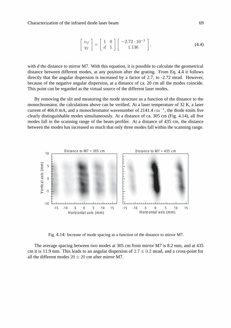
Characterization of the infrared diode laser beam 69
[αfyf
]=
[1 0d 1
] [−2.72 · 10−3
1.136
], (4.4)
with d the distance to mirror M7. With this equation, it is possible to calculate the geometricaldistance between different modes, at any position after the grating. From Eq. 4.4 it followsdirectly that the angular dispersion is increased by a factor of 2.7, to -2.72 mrad. However,because of the negative angular dispersion, at a distance of ca. 20 cm all the modes coincide.This point can be regarded as the virtual source of the different laser modes.
By removing the slit and measuring the mode structure as a function of the distance to themonochromator, the calculations above can be verified. At a laser temperature of 32 K, a lasercurrent of 466.0 mA, and a monochromator wavenumber of 2141.4 cm−1, the diode emits fiveclearly distinguishable modes simultaneously. At a distance of ca. 305 cm (Fig. 4.14), all fivemodes fall in the scanning range of the beam profiler. At a distance of 435 cm, the distancebetween the modes has increased so much that only three modes fall within the scanning range.
-15 -10 -5 0 5 10 15
Horizontal axis (mm)-15 -10 -5 0 5 10 15
-10
-5
0
5
10
Ver
tical
axi
s (m
m)
Distance to M7 = 305 cm Distance to M7 = 435 cm
Horizontal axis (mm)
Fig. 4.14: Increase of mode spacing as a function of the distance to mirror M7.
The average spacing between two modes at 305 cm from mirror M7 is 8.2 mm, and at 435cm it is 11.9 mm. This leads to an angular dispersion of 2.7 ± 0.2 mrad, and a cross-point forall the different modes 20± 20 cm after mirror M7.

70 Chapter 4
Astigmatism
During the measurements of the angular dispersion, another complication of this monochro-mator became clear. Fig. 4.14 clearly shows that the beam height remains constant at longerdistances from the mirror, but the beam width is severely decreased. This astigmatism is causedby the spherical mirrors M5 and M7, which are positioned under an angle with the optical axis.
Mirror M5 has to stay aligned to the grating and mirror M6, but by repositioning the exitmirror M8 and realigning M7, the angle between the beam and mirror M7 can be minimized.
M6
M7M8
S
original path new path
Fig. 4.15: Minimizing the astigmatism caused by mirror M7.
Measurements of the beam width as a function of the distance from mirror M7 show that,by repositioning M8, the astigmatism is reduced by nearly a factor of two (Fig. 4.16). With theoriginal lay-out of the monochromator, the horizontal beam size reduction was 3.1 mm/m, andwith the new lay-out, it has been reduced to 1.7 mm/m.
80 100 120 140 160 180 2008
9
10
11
12
13
14
15
16
17
80 100 120 140 160 180 2008
9
10
11
12
13
14
15
16
17
Bea
m s
ize
(mm
)
Distance to mirror M7 (cm)
Vertical beam size Horizontal beam size
Bea
m s
ize
(mm
)
Distance to mirror M7 (cm)
Vertical beam size Horizontal beam size
Fig. 4.16: (Left) astigmatism with original position of M7 and M8; (right) astigmatismwith repositioned M7 and M8.

5Characterization ofthe mid-infraredcavity ring downspectrometer

72 Chapter 5
5.1 Introduction
After completion of the ring down setup and adequate alignment of the diode laser, the firstmid-infrared cavity ring down experiments can be performed.
With the aid of two HeNe lasers, a visual diode laser, a CW CO laser and 6 diaphragms, aprocedure is developed to align the mirrors in the cavity, and the CO laser beam through thecavity.
The first aim will be to characterize the mode structure of the cavity. Then the diode laserwill be aligned through the cavity to perform the actual cavity ring down experiments.
5.2 Characterization of the optical cavity with the CO laser
The CW CO laser has a typical output power between 0.1 and 1 W, depending on the specificmode that is emitted. If the laser and the ring down cavity are aligned perfectly, the maximumlaser power that can build up inside the cavity is 1/(1-R) times the input power. With reflec-tivities between 0.997 and 0.999, the laser power inside the cavity can be 300 to 1000 timesthe input power. If the CO laser is aligned directly into the ring down cavity, the built up laserpower will instantly damage the multi-layer coating, and thereby destroy the optical cavity.
To limit the amount of laser power, the CO laser is aimed on a barium-fluoride (BaF2)window under an angle of 45 degrees. BaF2 reflects ca. 3 % at each surface, so, by only usingthe reflected power of the front side of the window, the laser power can be limited to a fewpercent of the total laser power. With the use of a diaphragm, the laser power can be furtherdecreased.
A triangular AC voltage of 100 V with a frequency of 100 Hz is applied over the piezo toperiodically scan the cavity length. After aligning the resulting few milliwatt of laser powerthrough the ring down cavity, the mode structure of the ring down cavity can be visualized onan oscilloscope (Fig. 5.1).
0 10 20 30 40 50-6
-5
-4
-3
-2
Sig
nal l
evel
(A
.U.)
Time (ms)
Fig. 5.1: Mode structure of the ring down cavity. The two large peaks belong to the funda-mental modes of the cavity. The smaller peaks in the middle belong to the odd higher ordermodes.

Characterization of the mid-infrared cavity ring down spectrometer 73
The large peaks in Fig. 5.1 belong to the fundamental modes, 150 MHz apart. The smallerpeaks approximately halfway the two peaks of the fundamental modes belong to the higherorder transverse TEM01 and TEM10 modes. Non-linearity and finite response time of the piezocrystals make that the peaks of the higher order transverse modes do not lie exactly halfway thefundamental modes.
If the cavity would be perfectly confocal, all the even transverse modes (m + n = evenEq. 2.4) should coincide with the fundamental modes. However, closer inspection of one ofthe fundamental modes in Fig. 5.1 clearly shows the even higher order transverse modes lyingbesides the fundamental mode (Fig. 5.2) Assuming a linear scan of the piezo and a free spectralrange of 150 MHz, the time base of Fig. 5.2 can be converted into a relative frequency scale.
-0.6
-0.4
-0.2
0.0
0.2
0.4
0.6
0.0 0.2 0.4 0.6 0.8 1.0
-1.5 -1.0 -0.5 0.0 0.5 1.0 1.5 2.0 2.5
Time (ms)
Sig
nal l
evel
(A
.U.)
TEM40/..
TEM20/11/02
TEM00
Frequency (MHz)
Fig. 5.2: Mode structure caused by error in cavity length.
The distance between two adjacent transverse modes can be calculated to be ca. 500 kHz.Calculating the mode spacing for two transverse modes from Eq. 2.7, with ∆q = +1 and∆(m+ n) = −2, reveals that the cavity length is ca. 5.2 mm too short.
By adding distance rings to the mirror holder, the transverse mode spacing can be deter-mined as a function of the cavity length (Fig. 5.3). These measurements show that a confocalcavity is obtained when the cavity length is increased by 3.8 mm. However, these measurementswere performed with an open cavity at one atmosphere. In vacuum conditions an extra cavitylength of 5.2 mm was preferable. Therefore, distance rings of 5.2 mm were added to the mirrorholds permanently.

74 Chapter 5
0 2 4 6 8-800
-600
-400
-200
0
200
400
600
Mod
e sp
acin
g (k
Hz)
Added cavity length (mm)
Fig. 5.3: Distance between even transverse modes as a function of the added cavity length.
After fine tuning of the cavity length, the ring down cavity mode structure was determinedfor a full piezo scan (Fig. 5.4). The voltage over the piezo was a 100 V, 20 Hz triangular wave.Clearly visible are the fundamental modes and the first order transverse modes halfway the freespectral range. The extra modes in between the fundamental and the higher order transversemodes are caused by the multi-mode operation of the CO laser.
0
2
4
6
8
10
-10 -5 0 5 10-0.2
0.0
0.2
0.4
0.6
0.8
1.0
1.2
1.4
Pie
zo V
olta
ge (
V)
Time (ms)
Sig
nal l
evel
(V
)
Fig. 5.4: Full piezo scan. The large peaks belong to the fundamental modes, and the smaller peakshalfway to the higher order transverse modes. The smallest peaks are caused by the fact that theCO laser was not perfectly single mode.

Characterization of the mid-infrared cavity ring down spectrometer 75
The line width of the fundamental modes is determined from Fig. 5.2 to be ca. 100 kHz,which means that the ring down cavity has a finesse of more than 1000. This very high finessecan be explained by the used wavelength region.
The finesse is mainly determined by the effective reflectivity of the mirrors. The effectivereflectivity is mostly determined by the real reflectivity, the surface roughness of the substrate,and the uniformity of the layers of the multi-layer coating which forms the reflective layer. Thelayer thickness of the layers forming the multi-layer coating, is a quarter of the wavelength ofthe applied laser light. Since the used wavelength is ca. 10 times longer than wavelengths inthe visible, the relative error in the layer thickness is a factor of 10 smaller. The same argumentapplies for the initial roughness of the used substrate. Here, again, the roughness is takenrelative to the used wavelength, and therefore it is a factor 10 smaller than the same substrateused in the visible.
For the applied wavelength the effective reflectivity does not differ much from the maximumreflectivity of the multi-layer coating, which leads to a very high finesse of the ring down cavity.
5.3 The diode laser beam and the ring down cavity
5.3.1 The mode structure with the diode laser
After alignment and characterization of the ring down cavity with the CO laser, the diode laserbeam has to be guided through the optical cavity. With an expected laser line width of 20 MHz,an output power of ca. 100 µW, of which less than 20 % reaches the cavity, and the maximumtransmission of the ring down cavity equal to the ratio of the cavity line width and the laser linewidth, the signal to noise ratio was expected to be between 1 and 10. Fig. 5.5 shows the detectorsignal and the piezo voltage as a function of time.
0.000 0.002 0.004 0.006 0.008-0.20
-0.15
-0.10
-0.05
0.00
0
2
4
6
8
10
12
14
16
18-600 -450 -300 -150 0 150 300 450 600
Det
ecto
r si
gnal
(V
)
Time (s)
Pie
zo v
olta
ge (
V)
150 MHz
Frequency (MHz)
Fig. 5.5: Mode structure of the ring down cavity obtained with the diode laser. The distancebetween the modes is less constant and some modes appear double because of the noise on thelaser wavelength.

76 Chapter 5
The large peaks in Fig. 5.5 at a roughly constant distance of 150 MHz are the TEM00 modes.The smaller peaks halfway are the odd transverse modes. Due to a very fast oscillation on thelaser wavelength some modes appear as double peaks. This oscillation makes that the cavitylength for which the cavity is resonant with the laser wavelength is slightly different for eachcavity sweep. Therefore, the modes of different sweeps do not coincide and the averaged peakheight of the signal decreases linearly with the number of averages, whereas the noise decreasesonly with the square root of the number of averages.
Another conclusion that can be drawn from this experiment is that the laser line width mustbe much smaller than 20 MHz. The measured mode structure is the convolution of the laserline width and the cavity line width. If the line width of the diode laser would be 20 MHz, thiswould show as broad peaks, approximately 15 % of the free spectral range wide. The addedsignal of 25 cavity sweeps (Fig. 5.6) shows an integral line width much closer to the predictedline width of 20 MHz. The laser wavelength of the diode is not formed by the de-excitation ofelectrons from one level in the conduction band to one level in the valence band, but the bandstructure consists of many sub levels and emitted laser light consists of de-excitation processesbetween many different sub-levels.
-0.002 0.000 0.002 0.004 0.006-0.8
-0.6
-0.4
-0.2
0.0
50 MHz
150 MHz
Envelope of 25 added signals
Det
ecto
r si
gnal
(V
)
Time (s)
Fig. 5.6: Envelope of 25 cavity sweeps, clearly showing the oscillation in the diode output fre-quency.
A clear disadvantage of this oscillation in the laser wavelength is that it prevents the cavityfrom being locked to the laser line, and thereby limits the repetition rate of the ring down signal.On the other hand, the fact that the line width is much smaller than the expected 20 MHzincreases the transmission of the cavity, and thereby the signal to noise ratio, which makes thealignment much easier.

Characterization of the mid-infrared cavity ring down spectrometer 77
5.3.2 Detuning the laser
Since the cavity length can not be locked to the laser wavelength, the cavity is scanned pe-riodically with a frequency of ca. 100 Hz over a length of several free spectral ranges. Thismakes that the cavity length is resonant to the laser wavelength several times each period of thepiezo voltage. During these resonances, ”ring up” takes place: the cavity is filled with photons.To start the exponential decay, the photons have to be stopped from entering the cavity fasterthan the expected ring down time. To obtain this, the laser has to be detuned to a non-resonantwavelength as soon as enough laser power has accumulated inside the cavity.
A level comparator connected to the detector creates a trigger signal when a mode has builtup inside the ring down cavity. The upper part of Fig. 5.7 shows the average of 200 times thebuildup and decay of the signal inside the cavity without detuning. This results in a more or lessGaussian shaped profile, which is the convolution of the time averaged laser line width with thescanning cavity mode.
-2x10⁻⁵ -1x10⁻⁵ -5x10⁻⁶ 0 5x10⁻⁶ 1x10⁻⁵ 2x10⁻⁵
Sig
nal (
A.U
.)
Time (s)
Fig. 5.7: Cavity mode with and without detuning. The upper curve is the average Airyprofile of the fundamental cavity mode, obtained by scanning the cavity length through thelaser wavelength. In the lower curve, at the moment there is enough laser power inside thecavity (vertical line), the laser is suddenly tuned to a wavelength halfway the free spectralrange, which effectively stops new photons from entering the cavity, and thereby starts theexponential decay.
The lower part shows the effect of the detuning of the laser wavelength. The laser is rapidlydetuned to a wavelength halfway the fundamental mode and the higher order transverse modes(Fig. 5.5). The profile is abruptly changed into an exponential decay when detuning has takenplace. The noisy feature at the top of the Gaussian peak is an artifact, caused by electronicfeedback of the trigger signal to the detector signal by a faulty connection.

78 Chapter 5
5.3.3 The exponential decay
Immediately after the laser is detuned to a non-resonant wavelength, the light intensity insidethe ring down cavity starts to decay exponentially. By averaging or adding several ring downtransients, the signal to noise ratio, and thereby the time span that can be used for the exponentialfit can be increased (Fig. 5.8)
The spread in the ring down time is determined by measuring the ring down time for a fixednumber of averages 100 times. Fig. 5.9 shows the development of the spread in the ring downtime as a function of the number of averaged ring down transients.
Most probably due to the low signal to noise ratio and the oscillation on the laser wavelength,the initial noise on a low number of averages of the ring down time is in the order of 10 % .Increasing the number of averages first decreases the error in the ring down time very fast, butfor a higher number of averages, the error seems to converge to ca. 1 % .
0 2 4 6 8 100.01
0.1
1
10
100 Detune moment
Sig
nal l
evel
(V
)
Time (10 -6 s)
10 averages 100 averages 1000 averages
Fig. 5.8: Exponential decay after detuning the laser.
10 100 1000
0.01
0.1
Spr
ead
in r
ing
dow
n tim
e (1
0-6 s
)
Number of averages
Fig. 5.9: Noise on ring down time as a function of the number of averages.

Characterization of the mid-infrared cavity ring down spectrometer 79
Eq. (1.18) dictates that the minimum detectable absorbance (= nσl) is equal to the productof (1−R) and the minimum detectable relative change in the ring down time (∆τ/τ ). The firstterm is determined by the constant reflectivity of 0.997 and is equal to 3 · 10−3. The last term ispresently limited to 10−2. This results in a detection limit for the total absorbance of 3 · 10−5.
5.3.4 The first mid-infrared spectroscopic cavity ring down measurements
The next step is to measure the ring down time as a function of the wavelength: cavity ring downspectroscopy. In order to create well defined absorption lines, the first spectroscopic ring downmeasurements will be performed on CO. CO has a well documented rovibrational spectrum inthe same wavelength region as silane and silane radicals, and is therefore often used to generatereference spectra to calibrate the wavelength of the diode laser.
Generation of a reference spectrum
A reference spectrum is generated with a conventional infrared laser absorption measurement.The laser beam is split into two beams. One of the beams is guided through a 5 inch longreference gas cell filled with 1 mbar CO, and the other beam is guided through an etalon. Bothbeams are detected individually.
By increasing the laser current, the wavelength of the laser is scanned over one of the modesof the diode. During the scan the laser is modulated at 1 kHz and the detector signal is led to alock-in amplifier that measures the second derivative of this signal. Fig. 5.10 shows the secondderivative of the absorption signal and the etalon fringes, which are 0.048 cm−1 apart. Theabsolute distance between the absorption lines is determined with the etalon signal, and withthe relative intensity and the handbook of infrared standards [50], all the lines can be identified.
0.135 0.145 0.155 0.165 0.175 0.185-0.10
-0.05
0.00
0.05
0.10
-0.10
0.00
0.10
0.20
0.30
0.40
0.50
2149.289252148.493922147.37775
2147.204972147.08158
2146.19841
Ref
eren
ce g
as s
igna
l (V
)
Eta
lon
sign
al (
V)
Laser current (A)
Fig. 5.10: IRLAS measurement on CO referernce gas cell and etalon.
The largest peak, at 2147.08158 cm−1, which falls largely outside the vertical scale ofthis graph, is of the most abundant isotope combination C12O16. One peak to the right, at

80 Chapter 5
2147.20497 cm−1, is of the C12O17 isotope, that has a relative abundancy of 0.04 % . The otherpeaks are of even rarer isotopes.
The first CRDS measurement
After the wavelength has been calibrated and the absorption lines are identified, the experimentis repeated with the cavity ring down spectrometer. The vacuum vessel is filled with 0.01 mbarCO and the diode laser is aligned through the ring down cavity. It turns out to be impossible tomeasure the absorption line around 2147.08158 cm−1 by the cavity ring down technique: thisline absorbs so strongly that no cavity mode can build up inside the cavity, and, consequently,no ring down transients can be recorded.
The C12O17 line around 2147.20497 cm−1 is much weaker, and therefore a better candidate.Fig. 5.11 shows a wavelength scan around the central wavelength of this line. Clearly visible isthe dip in the ring down time.
0.1508 0.1510 0.1512 0.1514
0.95
1.00
1.05
1.10
1.15
1.20
1.25
C12
O17
p = 0.010 mbar
2147,20497 cm -1
Rin
g do
wn
time
(10
-6 s
)
Laser current (A)
Fig. 5.11: Spectroscopic ring down measurement of CO.
With Eq. (1.17), the ring down time is converted to the absorbance (Fig. 5.12). The baselineclearly shows an sinusoidal signal. This is most likely caused by the low laser power and thelarge beam size of the diode laser beam, but the exact origin is not clear yet.
Due to the large beam size, the entrance mirror of the cavity is illuminated over a largesection. Therefore, the chance of exciting several transverse modes is much larger than withthe much smaller CO laser beam. Due to the small signal to noise ratio, the trigger level cannot be set too high, which allows both the fundamental and higher order transverse modesto generate trigger pulses and the subsequent ring down transients. However, the ring downtimes of higher order transverse modes differs from the ring down times of fundamental modes.During the wavelength scan, the relative contribution of different modes changes, which causesthe sinusoidal baseline.
The noise on the baseline limits the detection limit to ca. 5 · 10−5, or 5 · 10−7cm−1. Sincea systematic method to eliminate the alternating baseline could not be found, a sine functionis fitted manually. After subtraction of the fit from the ring down signal and a 5 point averag-ing over adjacent points, a much smoother signal is obtained (Fig. 5.13). With the identified

Characterization of the mid-infrared cavity ring down spectrometer 81
0.1508 0.1510 0.1512 0.1514
0
1x10 -4
2x10 -4
3x10 -4
4x10 -4
5x10 -4
Abs
orba
nce
Laser current (A)
Absorbance Background sine fit
Fig. 5.12: Ring down converted to absorbance + sine fit of thebackground.
absorption lines in Fig. 5.10 the laser current is converted in a relative frequency scale. A Gaus-sian fit through the corrected signal gives a resulting absorption line width of 202 MHz. For0.010 mbar CO at room temperature, the 1/e Doppler width should have been 175 MHz. Thedifference between the measured line width and the predicted line width can be explained bythe convolution of the absorption line and Gaussian laser line width of 50 MHz. The removalof the sine wave on the baseline brings the detection limit down to ca. 1 · 10−5, or 1 · 10−7cm−1
0.1508 0.1510 0.1512 0.1514
0
1x10⁻⁴
2x10⁻⁴
3x10⁻⁴
4x10⁻⁴
5x10⁻⁴-600 -400 -200 0 200 400 600
1/e width = 202 MHz
C12
O17
ptotal
= 0.010 mbar
2147.20497 cm -1
Abs
orba
nce
Laser current (A)
Frequency (MHz)
Fig. 5.13: Corrected absorbance and Gaussian fit.

82 Chapter 5
As a final test of the initial spectroscopic ring down measurements, the absorbance is mea-sured as a function of the CO pressure. The laser is set at the central wavelength of the2147.20497 cm−1 C12O17 line, and the ring down time is measured at different CO pressures.After each measurement the CO is pumped out of the vessel to measure τ0.
0.000 0.002 0.004 0.006 0.0080
1x10⁻⁴
2x10⁻⁴
3x10⁻⁴
4x10⁻⁴
Abs
orpt
ion
CO pressure (mbar)
Fig. 5.14: Absorption as a function of the CO pressure. The measured CO pressure isthe total CO pressure, while the measured absorption is only the absorption by the C12O17
isotope.
Fig. 5.14 shows that the absorbance is linear with the CO density and the detection limit ofthis C12O17 absorption line is reached for a total CO pressure of ca. 5 · 10−4 mbar. The relativeabundancy of C12O17 is estimated from the relative abundancy of O17 to be 4 · 10−4, whichgives a detection limit of the C12O16 absorption line at 2147.08158 cm−1 of ca. 1 · 10−7 mbar,or 3 · 109 cm−3 .

6General conclusions

84 Chapter 6
To address the complications associated with solar cells based on amorphous silicon (a-Si:H),e.g. the low growth rate and the degradation by exposure to light, it is necessary to come to acomplete insight in the complex chemistry inside silane discharges during the growth of thinlayers of amorphous silicon.
• The first preliminary conclusion that was drawn at the beginning of this project was thatthese insights could not be obtained with the available diagnostics at that time. It appearednot to be possible to monitor the time dependent density distributions of all the relevantspecies.
This thesis therefore deals with the development of a new diagnostic that can give insight inthe role of specific radicals during the growth of a-Si:H, the growth precursors and the growthmechanisms of dust particles.
The constructed mid-infrared cavity ring down spectrometer consists of a 1 meter long op-tical cavity, suspended in a vacuum vessel. By means of a 2-D manipulator a modular plasmachamber can be moved through the optical beam to acquire spatially resolved absolute radicaldensities. The conclusions that can be drawn from the initial tests of this setup are as follows.
• Measurements of the mode structure of the ring down cavity with a CW CO laser showthat the confocal cavity is mechanically and optically stable. At atmospheric pressure,the line profiles of the cavity modes are slightly broadened by the acoustic vibrations thatare coupled into the cavity from the background noise. Under vacuum this broadeningdisappears immediately and the resulting line width of the cavity modes is ca. 100 kHz(FWHM). The free spectral range (FSR) is 75 MHz, which, together with the half linewidth of the cavity modes, results in a total finesse for the fundamental transverse mode ofmore than 1000. This finesse is almost completely determined by the reflectivity losses,which are in the order of 10−3. Only for higher order transverse modes the diffractionlosses start to play a role, which results in a reduced peak heights for these modes.
• The new setup has, besides an improved sensitivity, also an improved implementationof spatially resolved measurements. The optical cavity, and thus the new diagnostic isconstructed without making any concessions to the discharge and vice versa. The firstdischarge configuration to be investigated, a capacitively coupled RF-discharge in a socalled plasma box, can be moved in two directions through the optical beam by meansof a 2-D manipulator to obtain spatially resolved, line integrated density profiles with asub-millimeter resolution in both directions.
• Due to the well designed multi-layer coating, the mirrors have a reflectivity between 0.997and 0.999 in the complete wavelength range from 4.2 to 5.6 µm . In this wavelength rangeall the important species in silane discharges have known rovibrational absorption spectra:all the mono-silane radicals (SiH, SiH2, and SiH3), the disilanes Si2H5 and Si2H6, andthe most important ionic species SiH3
− and SiH3+. Because of the similarity of the Si-H
bonds, also the larger clusters (e.g. Si3Hm) are expected to have rovibrational absorptionspectra in this region, and dust particles are expected to exhibit, besides the molecularabsorption lines, also a-Si:H bulk absorption features in the same wavelength region.
Another preliminary conclusion that could be drawn in the beginning phase of this project wasthat the only suitable light source for the mid-infrared cavity ring down experiments is thehelium cooled CW diode laser system. Extensive research on the infrared laser beam revealedthe following facts.

General conclusions 85
• The divergence of the laser beam at the end facet of the diode is somewhere in between 30and 40o. An off-axis parabolic (OAP) mirror is used to transform the divergent beam intoa parallel beam. Due to the distance from the diode to the OAP mirror and the size of theOAP mirror, the diameter of the beam after reflection on the OAP mirror is determinedby the diameter of the mirror, which is 35 mm.
• Since most mid-infrared laser diodes are multi-mode diodes, a monochromator is usedto select one of the modes. However, the layout of the available monochromator and thesize of the used mirrors and grating are not suitable for a laser beam with a diameter of35 mm. Therefore, the beam is clipped many times inside the monochromator and has arectangular shape of ca. 17× 14 mm (H×W) at the exit plane of the monochromator.
• The overall transmission of the monochromator is reduced to less than 20 % because ofthe subsequent clipping. A single mode of the diode has a typical laser power before itenters the monochromator of ca. 100 µW. Due to the losses inside the monochromatorand some extra losses in between the monochromator and the cavity, only ca. 10 µWreaches the entrance mirror of the ring down cavity.
• As a consequence of the use of spherical mirrors inside the monochromator under anangle with the optical axis, the beam becomes astigmatic. The vertical extent of the beamis nearly parallel, but horizontally the beam has a focal point at ca. 8.2 m after the lastspherical mirror of the monochromator.
Besides the low output power, the other major drawback of this type of diode laser is the factthat it is a CW laser and conventional methods to chop the laser beam fast enough to induce asingle exponential decay do not work. Therefore, a new method to chop the laser beam had tobe developed.
• The new method, where the ring down cavity is tuned to the laser wavelength and, as soonas there is enough laser power inside the cavity, the laser is detuned from the cavity modereaches a full decoupling of the laser from the cavity within several tens of nanoseconds.
• The resulting decay of the light intensity inside the cavity is a single exponential decaywith a ring down time which is only determined by the reflectivity of the mirrors.
• The obtained ring down times in the wavelength region covered by the diode used forthe first CRDS experiments range from ca. 800 ns up to 1.5 µs, which corresponds to thespectral reflectivity of the mirrors.
The first spectroscopic mid-infrared cavity ring down experiments were performed on CO,which has a well documented rovibrational spectrum in the same wavelength region as silane.The main conclusions that could be drawn from these experiments are as follows:
• The principle of performing mid-infrared CRDS experiments with a CW diode laser anda tuned confocal cavity does work.
• The upper limit of the absorption is determined by the demand that a certain intensityshould be able to build up inside the cavity before the laser is detuned and the exponentialdecay is started. Therefore, absorption lines that are too strong and thereby prevent acavity mode to build up to a certain level cannot be detected. The maximum reduction inring down time that can be measured is approximately 40 %, which sets the upper limitof the sensitivity to ca. 2 · 10−3 or 2 · 10−5 cm−1.

86 Chapter 6
• The sensitivity is limited by a ripple on the base line to ca. 5·10−5 or 5·10−7 cm−1. Thisripple is caused by the low laser output and the low transmission of the monochromatorwhich prevents the use of small diaphragms in front of the ring down cavity. Therefore,not only the axial modes are excited but also the higher order transverse modes. Thesehigher order modes have a shorter decay time because of the higher diffraction losses.The measured ring down time is an average of the ring down times of the different excitedmodes The contribution of the modes shifts as the wavelength is scanned, which causesthe ripple in the ring down time.
• Subtraction of a manually fitted sine function through the base line reduces the noiseand increases the sensitivity to ca. 1 · 10−5 or 1 · 10−7 cm−1. Taking into account therelative abundance of the measured C12O17 isotope, which is estimated from the relativeabundance of O17 to be approximately 4 · 10−4, this sensitivity corresponds to a pressureof ca. 1 · 10−7 mbar, or a density of 3 · 109 cm−3.
This is already 2 orders of magnitude more sensitive than the most sophisticated conven-tional infrared diode laser absorption measurements. Presently, the sensitivity is limited by theminimum detectable change in ring down time. With a redesign of the monochromator it shouldbe possible to increase the amount of laser power at the entrance mirror of the cavity by at leasta factor of three. It should also be possible to further suppress the astigmatism. Then the beamdiameter can be reduced to a few millimeter. The increase of output power and beam qualitywill make it possible to put a diaphragm in front of the cavity. In this way it will become pos-sible to limit the modes that can be excited in the cavity to only the fundamental mode. Theminimum detectable change in ring down time will then be reduced to 10−3, which will bringthe detection limit down to 3 · 10−6.
If necessary, the detection limit can be further improved by obtaining better mirrors. Oneextra nine in the reflectivity (e.g. 0.999→ 0.9999) will decrease both the factor (1−R) and theminimum detectable relative change in ring down time by one order of magnitude. The mini-mum detectable change in absorbance, which is the product of these two factors, will thereforego down by two orders of magnitude. The resulting detection limit will be smaller than 1 ·10−7,which should be more than adequate to detect all the relevant species in a silane discharge.

Bibliography
[1] E. Hamers, Plasma deposition of hydrogenated amorphous silicon, Utrecht (1998)
[2] E. Kessels, Remote plasma deposition of hydrogenated amorphous silicon, Universiteits-drukkerij Technische Universiteit Eindhoven, Eindhoven (2000)
[3] P. Roca i Cabaroccas, P. St’ahel, S. Hamma, Y. Poissant, Stable single junction p-i-n solarcells with efficiencies approaching 10%, Proc. 2nd world conference on photovoltaic solarenergy conversion, Vienne 1998, p. 355
[4] C. N. Banwell, Fundamentals of molecular spectroscopy, McGraw-Hill Book Company,London (1972)
[5] G.Herzberg, Infrared and Raman spectra, D. van Nostrand Company, New York (1945)
[6] A. Cabana, L. Lambert, C. Pepin, High resolution infrared measurements on the ν3
vibration-rotation band of 28SiH4, J. Mol. Spec. 43, 429 (1972)
[7] A. Cabana, D. L. Gray, A. G. Robiette, G. Pierre, Analysis of the ν3 and ν1 infrared bandsof SiH4, Mol. Phys. 36, 1503 (1978)
[8] A. E. Douglas, The spectrum of silicon hydride, Can. J. Phys. 35, 71 (1957)
[9] R. D. Verma, The spectrum of SiH and SiD, Can. J. Phys. 43, 2136 (1965)
[10] G. Herzberg, A. Lagerqvist, B. J. McKenzie, Absorption spectrum of SiH in the vacuumultraviolet, Can. J. Phys. 47, 1889 (1969)
[11] J. C. Knights, J. P. M. Schmitt, J. Perrin, G. Guelachvili, High resolution absorption andemission spectroscopy of a silane plasma in the 1800-2300 cm−1range, J. Chem. Phys.76, 3414 (1982)
[12] P. B. Davies, N. A. Isaacs, S. A. Johnson, D. K. Russell, Detection of SiH(X 2Π) funda-mental and hot band transitions by diode laser absorption spectroscopy, J. Chem. Phys.83, 2060 (1985)
[13] I. Dubois, The absorption spectrum of the free SiH2 radical, Can. J. Phys 46, 2485 (1968)
[14] L.Fredin, R. H. Hauge, Z. H. Kafafi, J. L. Margrave, Matrix isolation studies of siliconatoms with molecular hydrogen. The infrared spectrum of silylene, J. Chem. Phys. 82,3542 (1985)
87

88
[15] C. Yamada, H. Kanamori, E. Hirota, N. Nishiwaki, N. Itabashi, K. Kato, T. Goto, Detec-tion of the silylene ν2 band by infrared diode laser kinetic spectroscopy, J. Chem. Phys.91, 4582 (1989)
[16] C. Yamada, E. Hirota, Detection of the Silyl Radical SiH3 by Infrared diode-laser spec-troscopy, Phys. Rev. Lett. 56, 923 (1986)
[17] Y. Sumiyoshi, K. Tanaka, T. Tanaka, Diode laser spectroscopy of SiH3 in the 4.5 µmregion, Appl. Surf. Sci. 79/80, 471 (1994)
[18] Finholt, Bond, Wilzbach, Schlesinger, J. Am. Chem. Soc. 69, 2692 (1947)
[19] H. S. Gutowsky, E. O. Stejskal, The infrared spectrum of disilane, J. Chem. Phys. 22, 939(1953)
[20] P. A. Hamilton, J. Vaghjiani, The high-resolution infrared spectrum of the nu6 band ofdisilane, J. Mol. Spec. 151, 12 (1992)
[21] P. A. Hamilton, J. Vaghjiani, The high-resolution infrared spectrum of the nu8 band ofdisilane, J. Mol. Spec. 157, 369 (1993)
[22] D. C. McKean, On the assignment of SiH and SiD stretching frequencies: a reanalysisof the ν7 bands of Si2H6 and Si2D6 and a harmonic local mode force field for disilane,Spectr. Acta 48A, 1335 (1992)
[23] P. D. Lightfoot, R. Becerra, A. A. Jemi-Alade, R. Lesclaux, The UV absorption spectrumof SiH3, Chem. Phys. Lett. 180, 441 (1991)
[24] H. Toyoda, M. Goto, M. Kitagawa, T. Hirao, H. Sugai, Simple direct monitoring of SiH3
radical and particulates in a silane plasma with ultraviolet transmission spectroscopy,Jap. J. Appl. Phys. 34, L 448 (1995)
[25] M.G.H. Boogaarts, P.J. Bocker, W.M.M. Kessels, D.C. Schram, M.C.M. van der Sanden,Cavity ring down detection of SiH3 on the broadband A 2A1’ ← X 2A1 transition in aremote Ar-H2-SiH4 plasma, Chem. Phys. Lett. 326, 400 (2000)
[26] M. Shen, Y. Xie, H. F. Schaefer III, The silyl anion (SiH−3 ): Harmonic vibrational fre-quencies and infrared intensities predicted at the SCF, CISD, and CCSD levels of theorywith substantial basis sets, J. Chem. Phys. 93, 8098 (1990)
[27] D. M. Smith, P. M. Martineau, P. B. Davies, Infrared laser absorption spectroscopy of theSiH+
3 cation, J. Chem. Phys. 96, 1741 (1992)
[28] N. Itabashi, K. Kato, N. Nishiwaki, T. Goto, C. Yamada, E. Hirota, SiH3 radical densityin pulsed silane plasma, Jap. J. Appl. Phys. 29, 585 (1990)
[29] N. Itabashi, N. Nishiwaki, M. Magane, T. Goto, A. Matsuda, C. Yamada, E. Hirota, Dif-fusion coefficient and reaction rate constant of the SiH3 radical in silane plasma, Jap. J.Appl. Phys. 28, L325 (1989)

BIBLIOGRAPHY 89
[30] N. Itabashi, N. Nishiwaki, M. Magane, S. Naito, T. Goto, A. Matsuda, C. Yamada, E.Hirota, Spatial distribution of SiH3 radicals in RF silane plasma, Jap. J. Appl. Phys. 29,L505 (1990)
[31] H. Nomura, A. Kono, T. Goto, Effect of dilution gases on the SiH3 radical density in anRF SiH4 plasma, Jap. J. Appl. Phys. 33, 4165 (1994)
[32] N. Itabashi, K. Kato, N. Nishiwaki, T. Goto, C. Yamada, E. Hirota, Measurement of theSiH3 radical density in silane plasma using infrared diode laser absorption spectroscopy,Jap. J. Appl. Phys. 27, L1565 (1988)
[33] Y. Yamamoto, H. Nomura, T. Tanaka, M. Hiramatsu, M. Hori, T. Goto, Measurement ofabsolute densities of Si, SiH and SiH3 in electron cyclotron resonance SiH4/H2 plasma,Jap. J. Appl. Phys. 33, 4320 (1994)
[34] A. O’Keefe, D. A. G. Deacon, Cavity ring-down optical spectrometer for absorption mea-surements using pulsed laser sources, Rev. Sci. Instr. 59, 2544 (1988)
[35] D. Romanini, A. A. Kachanov, N. Sadeghi, F. Stoeckel, CW cavity ring down spec-troscopy, Chem. Phys. Lett. 264, 316 (1997)
[36] G. Meijer, M. G. H. Boogaarts, R. T. Jongma, D. H. Parker, Coherent cavity ring downspectroscopy, Chem. Phys. Lett. 217, 112 (1994)
[37] K. W. Aniolek, P. E. Powers, T. J. Kulp, B. A. Richman, S. E. Bisson, Cavity ringdownlaser absorption spectroscopy with a 1 KHz mid infrared periodically poled lithium nio-bate optical parametric generator/optical parametric amplifier, Chem. Phys. Lett. 302,555 (1999)
[38] R. Engeln, G. v. Helden, G. Berden, G. Meijer, Phase shift cavity ring down absorptionspectroscopy, Chem. Phys. Lett. 262, 105 (1996)
[39] R. Engeln, G. Meijer, A Fourier transform cavity ring down spectrometer, Rev. Sci. Instr.67, 2708 (1996)
[40] R. Engeln, G. Berden, R. Peeters, G. Meijer, Cavity enhanced absorption spectroscopyand cavity enhanced magnetic rotation spectrosopy, Rev. Sci. Instr. 69, 3763 (1998)
[41] H. Kogelnik, T. Li, Laser beams and resonators, Appl. Opt. 5, 1550 (1966)
[42] W. Demtroder, Laser spectroscopy, Springer-Verlag, Berlin (1982)
[43] G. D. Boyd, H. Kogelnik, Generalized confocal resonator theory, Bell Syst. Tech. J. 41,1347 (1962)
[44] J. T. Hodges, J. P. Looney, R. D. van Zee, , J. Chem. Phys. 105, 10278 (1996)
[45] E. Hecht, Optics, Addison-Wesley Publishing Company (1974)
[46] L. Boufendi, A. Bouchoule, Particle nucleation and particle growth in a low-pressureargon-silane discharge, Plasma Sources Sci. Techn. 3, 262 (1994)

90
[47] A. Bouchoule, A. Plain, L. Boufendi, J. Ph. Blondeau, C. Laure, Particle generation andbehaviour in a silane-argon low pressure discharge under continuous or pulsed radiofrequency excitation, J. Appl. Phys. 70, 1991 (1991)
[48] W. W. Chow, S. W. Kock, M Sargent III, Semiconductor-laser physics, Springer Verlag,Berlin Heidelberg (1994)
[49] J. Hecht, The laser guidebook, McGraw-Hill, New York (1992)
[50] G. Guelachvili, K. Narahari Rao, Handbook of infrared standards, Academic Press, Lon-don (1986)

91
Summary
In the field of renewable energy, a lot is expected from photovoltaic (PV) solar cells based onthin layers of hydrogenated amorphous silicon (a-Si:H), which can be deposited by plasma en-hanced chemical vapor deposition (PECVD). So far, however, the production costs of these solarcells are high because of the low growth rate of a-Si:H. Furthermore, the efficiency decreasessubstantially under exposure to sunlight.
The solutions for the low growth rate as well as for the light induced degradation are ex-pected to be found in the silane discharges used to grow these solar cells. However, these dis-charges are chemically and physically very complex. The interaction of many different species(neutral and charged) forms the basis of the deposition of the thin layers of silicon. In orderto get a better understanding of all the important processes inside these discharges it is neces-sary to know the time resolved density distributions of all the relevant species. However, thediagnostics used in the field of plasma physics so far are not capable of providing the necessarydata. Therefore a new diagnostic is needed.
A very interesting spectroscopic region to perform absorption or emission measurementson discharges containing molecular species is the mid-infrared. The masses of the atoms inthe molecule and the binding forces between these atoms result in rovibrational spectra withtypical transition energies of some tenths of an eV. The available light sources, detectors, andother optical equipment make that diagnostics operating in this wavelength region have a lim-ited sensitivity. In 1988 a new method to perform absorption measurements was introduced:cavity ring down spectroscopy (CRDS). Rather than measuring the magnitude of absorption,CRDS is based on the measurement of the rate of absorption of the light intensity inside anoptically stable cavity, which is built around the gas or discharge to be analyzed. Sensitivitiesthat can be obtained with this technique are orders of magnitude higher than those obtained withconventional absorption measurements, without the loss of spatial and time resolution.
This thesis reports about the design, realization, and implementation of a mid-infrared cavityring down spectrometer. The realized setup is comprised of a 1 meter long, mechanically stable,confocal cavity suspended in a vacuum vessel. The mirrors have a reflectivity between 0.997and 0.999 over the complete wavelength range from 4.2 to 5.6 µm . All the relevant speciesinside silane discharges have rovibrational absorption spectra in this wavelength region. Theinner diameter of the cavity is ca. 35 cm, which allows for the capacitively coupled RF-dischargein the so called plasma box configuration to be moved through the optical beam by means ofthe 2-D manipulator.
The first results obtained with a CO laser show that the confocal cavity has a free spectralrange of 75 MHz and the peak width of the fundamental cavity mode is ca. 100 kHz (FWHM).This results in a finesse of more than 1000, which is fully determined by the reflectivity ofthe mirrors. For the higher order transverse modes the diffraction losses start to become more

92
important, which results in broader peaks with a reduced peak height.The only available light source to perform spectroscopic cavity ring down experiments in
the mid-infrared is the helium cooled diode laser system. Extensive research on the beamcharacteristics of this laser revealed that the nearly circular beam has a diameter of 35 mm beforeit enters the monochromator. The available monochromator is not designed for this size of laserbeams and therefore clips the beam many times before it leaves the monochromator. This resultsin an overall transmission of the monochromator of less than 20 %. Of the typical output powerof the laser diode of ca. 100 µW, only ca. 10 µW reaches the ring down cavity. After aligningthe diode laser beam through the ring down cavity, the mode structure of the cavity lookeddifferent from the mode structure obtained with the CO laser. This can only be attributed toa jitter on the laser wavelength of the diode laser, combined with the low laser output and thelarge beam diameter. Due to the low laser power it is not possible to use diaphragms in frontof the cavity to limit the size of the laser beam. Therefore not only the fundamental mode, butalso a number of higher order transverse modes are excited.
One of the major disadvantages of the use of the infrared diode laser system to performCRDS experiments is the fact that it is a CW laser. In this wavelength region, conventionalmethods to chop a laser beam to stop the photons from entering the ring down cavity and startthe exponential decay do not work. In the newly developed method to stop the photons fromentering the cavity, the cavity length is tuned to the laser wavelength by a piezo. As soon as thecavity is resonant with the laser, a standing wave starts to build up inside the cavity. When thelight intensity inside the cavity is high enough, the laser wavelength is detuned to a wavelengthabout halfway the free spectral range of the ring down cavity. This detuning only requires achange in current through the laser diode of ca. 10−5 A, which makes this method very fast andvery stable. A full decoupling of the laser from the cavity can be obtained in less than 100 ns.
The first mid-infrared spectroscopic ring down experiments on CO showed that the princi-ple of tuning the cavity and detuning the laser does work. The upper limit of the detectableabsorbance nσl is determined by the fact that for a too strong absorption no standing wavescan build up inside the cavity. This sets the maximum detectable absorbance to ca. 2 · 10−3 or2·10−5 cm−1. A ripple on the baseline of the spectroscopic ring down signal caused by the jitteron the laser wavelength and the large beam size, sets the lower detection limit of the absorbanceto 5 · 10−5 or 5 · 10−7 cm−1. Subtraction of a sine fit through the baseline increases thesensitivity to 1 · 10−5 or 1 · 10−7 cm−1, which corresponds to a CO density of ca. 3 · 109 cm−1.
From these results it can be concluded that the new mid-infrared cavity ring down spec-trometer is a non-intrusive diagnostic which is two orders of magnitude more sensitive thanconventional infrared absorption measurements, without any loss of spatial and time resolution.

93
Samenvatting
De fotovoltaische zonnecel gemaakt van gehydrogeneerd amorf silicium is een veelbelovendekandidaat-leverancier van schone energie. De kosten van deze zonnecellen, die worden gepro-duceerd door middel van ’plasma enhanced chemical vapour deposition’, zijn momenteel nogerg hoog. Bovendien zakt de efficientie van de zonnecel sterk in wanneer deze wordt bloot-gesteld aan zonlicht.
Verwacht wordt dat de oplossingen voor zowel de lage groeisnelheid als ook de degradatiedoor zonlicht gevonden kunnen worden in de silaanplasma’s die gebruikt worden om deze zon-necellen te fabriceren. Echter, dit type plasma is zowel fysisch als chemisch zeer complex. Deinteractie tussen een groot aantal verschillende deeltjes (neutraal en geladen) vormt de basisvoor de groei van de dunne lagen amorf silicium. Om tot een beter begrip van alle belang-rijke processen in dit soort gasontladingen te komen is het noodzakelijk om de tijdsopgelostedichtheidsprofielen van alle relevante deeltjes in het plasma te kennen. Met de diagnostiekendie tot nu toe in de plasmafysica worden gebruikt is het niet mogelijk om dit te bewerkstelligen.Daarom is het nodig een nieuwe diagnostiek te ontwikkelen.
Het meest interessante deel van het spectrum voor absorptie- of emissie-metingen aan plas-ma’s die molekulaire deeltes bevatten is het mid-infrarood. De massa’s van de verschillendeatomen in het molekuul en de bindingssterkte tussen deze atomen resulteren in een rovibra-tioneel spectrum met typische overgangsenergieen van enkele tienden van een electronvolt. Debeschikbare lichtbronnen, detectoren en overige optische instrumentatie zorgen er echter voordat diagnostieken werkend in dit golflengtegebied een beperkte detectielimiet hebben. In 1988werd een nieuwe methode om absorptiemetingen te verrichten geıntroduceerd: cavity ring downspectroscopie. In plaats van de bepaling van de absolute afname van de lichtintensiteit wordt bijcavity ring down spectroscopie gekeken naar de vervaltijd van de lichtintensiteit in een optischstabiele cavity, die is opgebouwd rond het te onderzoeken gas of plasma. De gevoeligheden diemet deze techniek behaald kunnen worden zijn ordes groter dan die behaald met conventioneleabsorptiespectroscopie, zonder verlies van ruimtelijke en tijdsoplossing.
Dit proefschift behandelt het ontwerp, de realisatie en de implementatie van een mid-infra-rood cavity ring down spectrometer. De kern van de gerealizeerde meetopstelling is een 1 meterlange, mechanisch stabiele, confocale cavity die is opgehangen in een vacuumvat. De spiegelshebben een reflectiviteit varierend van 0.997 tot 0.999 over het gehele golflengtebereik van 4.2tot 5.6 µm . Alle relevante deeltjes in een silaanplasma hebben rovibrationele absorptiespectrain dit golflengtegebied. De binnendiameter van de cavity is 35 cm. Hierdoor is het mogelijkeen zogenaamde ”plasma-box” met het capacatief gekoppelde RF-plasma met behulp van een2-D manipulator door de optische bundel te bewegen.
De eerste resultaten die behaald zijn met een CO laser tonen aan dat de optische cavity eenvrij spectraal bereik heeft van 75 MHz. De piekbreedte van de fundamentele cavitymode is ca.

94
100 kHz (FWHM). Dit resulteert in een finesse van meer dan 1000, die geheel wordt bepaalddoor de reflectiviteit van de spiegels. Voor de hogere orde transversale modes beginnen dediffractieverliezen een belangrijkere rol te spelen, waardoor de pieken breder en lager worden.
De enige beschikbare lichtbron waarmee de spectroscopische cavity ring down metingenkunnen worden uitgevoerd in het mid-infrarood is het helium gekoelde diodelaser-systeem. In-tensief onderzoek aan de bundeleigenschappen van deze laser toonden aan dat de bijna rondebundel een diameter heeft van 35 mm voordat hij de monochromator in gaat. De beschikbaremonochromator is niet berekend op laserbundels met deze afmetingen, waardoor grote delenvan de bundel verloren gaan voordat de bundel de monochromator weer verlaat. Dit resulteertin een totale transmissie van de monochromator van minder dan 20 %. Van het typische uit-gangsvermogen van de diodelaser van 100 µW bereikt slechts ca. 10 µW daadwerkelijk de op-tische cavity. Na uitlijning van de diodelaserbundel door de optische cavity zag de resulterendemodestructuur van de cavity er anders uit dan gemeten met de CO laser. Dit kon alleen wordenverklaard met een kleine hoeveelheid ruis op de golflengte van de diodelaser gecombineerd methet lage laservermogen. Door dit lage laservermogen was het niet mogelijk om de afmeting vande laserbundel te beperken met diafragma’s voor de optische cavity, wat direct resulteert in deexcitatie van een groot aantal cavity modes, in plaats van alleen de fundamentele mode.
Een van de grootste bezwaren van het gebruik van een diodelaser voor CRDS experimentenis het feit dat het een continue laser is. De gebruikelijke methodes om een abrupt einde temaken aan de instroom van fotonen in de cavity werken niet in dit golflengtegebied. Bij denieuw ontwikkelde methode wordt de lengte van de cavity met behulp van een piezo afgestemdop de golflengte van het laserlicht. Op het moment dat de cavity resonant is met de golflengtevan de laser begint een staande golf zich op te bouwen in de cavity. Zodra de intensiteit vanhet laservermogen in de cavity hoog genoeg is, wordt de golflengte van de laser verstemd naareen golflengte ongeveer halverwege het vrije spectrale bereik. De benodigde extra stroom doorde diode om dit verstemmen te bewerkstelligen is slechts 10−5 A, waardoor dit een erg snelleen stabiele manier is om abrupt de toevoer van fotonen te onderbreken. De cavity en de laserworden met deze methode in minder dan 100 ns volkomen ontkoppeld.
De eerste spectroscopische cavity ring down metingen laten zien dat de methode van hetafstemmen van de cavity en het verstemmen van de golflengte van de laser daadwerkelijk werkt.De bovenlimiet van de te detecteren absorptie nσl wordt bepaald door het feit dat voor een testerke absorptie geen staande golven opbouwen in de cavity. Dit limiteert de te detecterenabsorptie tot maximaal 2 · 10−3, of 2 · 10−5 cm−1. Een rimpel op de achtergrond van hetspectroscopische ring down signaal, veroorzaakt door de ruis op de golflengte van de laseren het lage laservermogen limiteren de ondergrens van de te meten absorptie tot 5 · 10−5, of5 · 10−7 cm−1. Na aftrek van een handmatig aangepaste sinusfunctie wordt de detectielimitteruggebracht tot 1 · 10−5, of 1 · 10−7 cm−1, wat correspondeert met een CO dichtheid van ca.3 · 109 cm−3.
Hieruit kan worden geconcludeerd dat de nieuwe mid-infrarood cavity ring down spec-trometer een nieuwe diagnostiek is die, zonder het te meten gas of plasma te beınvloeden, eengevoeligheid haalt die twee ordes hoger is dan conventionele infrarood absorptiespectroscopie,zonder afbreuk te doen aan het ruimtelijke en tijdsoplossend vermogen.

95
Dankwoord
Allereerst wil ik mijn ouders bedanken voor alle kansen en vrijheid die ze me gegeven hebbenom mijn eigen weg te kiezen en me te ontwikkelen tot wat ik nu ben. Frits de Hoog en GerritKroesen wil ik bedanken voor het vertrouwen en de grote vrijheid die ze mij gegeven hebbenin het nastreven van mijn doelen. Maarten Boogaarts en Richard Engeln wil ik bedanken voorhun inspiratie en hun hulp bij het ontwikkelen van het hele cavity ring down concept.
Zonder het uitstekende werk van de alle betrokken groepen bij de GTD had deze nieuweopstelling nooit gerealiseerd kunnen worden. In dit kader wil ik speciaal Erwin Dekkers enPeer Brinkgreve bedanken voor het uitmuntende ontwerp en de fijne manier van samenwerken,Evert Ridderhof voor de perfecte ondersteuning bij de PLC, en Charlotte Groothuis voor haarsteun bij het africhten van de diode laser, die ze deels in haar privetijd leverde. Marius Bogersen alle mensen van de faculteitswerkplaats wil ik bedanken voor hun vakkundige en snelletechnische oplossingen. Fred van Nijmwegen, Gerard Harkema, Roel Smeets, Carine van derLinden en Judith van de Griendt voor hun geweldige werk aan het TUeDACS systeem.
Binnen de groep wil ik uiteraard eerst Loek Baede, Lambert Bisschops en Hans Freriksbedanken voor alle technische en anderssoortige ondersteuning. De mede (ex)-aio’s GeertSwinkels, Marc van der Grift, Wilfred Hoeben, Gerjan Hagelaar, Jean-Charles Cigal, CarolMaurice, Gabriela Paeve, Xiao-Yan Zhu en Mikhail Sorokine wil ik bedanken voor hun multi-culturele gezelligheid. In dit kader gaat speciale dank uit naar Daiyu Hayashi. De overige(ex-)groepsleden Wijnand Rutgers, Eddie van Veldhuizen, Winfred Stoffels, Tarik Hbid, EvaStoffels, Nandini Gupta, Rina Boom en Marianne van den Elshout voor alles wat ze voor megedaan hebben. Uiteraard gaat mijn dank ook uit naar de stagiares Wouter Brok en Mihari vooral het werk dat ze verzet hebben. I would like to thank Pere Roca i Cabaroccas for his intro-duction to real solar cells, and the wonderful time in Paris. Naast Frits en Gerrit, wil ik ookAnton Tijhuis en mijn tweede promotor Richard van de Sanden bedanken voor hun kritische enopbouwende kijk op dit proefschrift. Alle leden van de groep ETP wil ik bedanken voor hunbelangstelling en steun op het gebied van de silaanplasma’s en de cavity ring down techniek.Speciale dank gaat uit naar de mensen van het modellenburo voor hun steun bij het vervaardigenvan dit proefschift. Alle leden van het Fysisch Genootschap Nwyvre wil ik bedanken voor degezelligheid en het draaglijk maken van de zware studententijd en het ondraaglijk maken van devrijdagochtenden. Alle vrienden en familie bedank ik voor alle steun die ze me gegeven hebbenen die ik vooral het laatste half jaar heel goed kon gebruiken. Een heel bijzondere plaats wordthierbij ingenomen door mijn schoonouders.
Terugkijkend op mijn hele promotietijd kan ik alleen maar concluderen dat ik dit einde nooitgehaald zou hebben zonder die ene persoon, die als enige echt weet hoe diep ik soms gegaanben en nooit van mijn zijde week. Emmely, ontzettend bedankt dat je me toch elke keer weeraan het lachen kreeg.

96
Curriculum vitae
PERSONALIA
Naam HemerikVoornamen Marcel MauriceGeboortedatum 15 november 1972Geboorteplaats Leiden
OPLEIDINGEN
1978 - 1985 Basisschool ’Samen Onderweg’ te Leiderdorp1985 - 1986 Brugklas, Christelijk Lydeum ’Dr. W.A. Visser ’t Hooft’
te Leiderdorp1986 - 1991 V.W.O., ’Het Christelijk Lyceum’ te Alphen a/d Rijn1991 - 1996 Studie technische natuurkunde aan de Technische
Universiteit Eindhoven: Interne stage binnen de vakgroep Fysica van
Oppervlakken en Grenslagen: Externa stage bij het FOM instituut voor
plasmafysica ’Rijnhuizen’: Afstudeerstage binnen de vakgroep Elementaire
Processen in Gasontladingen: Twee jaar bestuurslid van de Zweefvliegclub
Eindhovense StudentenDiploma behaald op 18 december 1996
1997 - 2001 Promotieonderzoek binnen de vakgroep ElementaireProcessen in Gasontladingen, faculteit Technische Natuurkunde,Technische Universiteit Eindhoven: 1-9-1999 - 31-10-1999 Stage aan l’Ecole Polytechnique
Palaiseau