design of digital circuits(s2) modelling and simulation
TRANSCRIPT

2.
Design of Digital Circuits(S2)
Chapter 1, Part 2
Modelling and SimulationSection 1.3 Delay Time Tolerance
to 1.6 Sequential Circuits
Prof. G. Kemnitz
Institute of Informatics, Clausthal University of TechnologyMay 14, 2012
Prof. G. Kemnitz · Institute of Informatics, Clausthal University of Technology May 14, 2012 1/129

2.
Delay Time Tolerance1.1 Glitches1.2 Delay model1.3 Delay tolerance region1.4 Run Time Analysis1.5 Exercises
Register2.1 Sampling with Registers2.2 VHDL sampling process2.3 Processing + Sampling2.4 Register transfer function2.5 Clock skew2.6 Exercises
Prof. G. Kemnitz · Institute of Informatics, Clausthal University of Technology May 14, 2012 1/129

2.Asynchronous input
3.1 Sampling a single bit3.2 Switch de-bouncing3.3 Asynch. initialization3.4 Parallel interface3.5 Exercises
Sequential circuit4.1 Finite state machine4.2 Automaton ⇒ VHDL4.3 System crash4.4 Combination lock4.5 Operation graph4.6 Quadrature encoder
Prof. G. Kemnitz · Institute of Informatics, Clausthal University of Technology May 14, 2012 1/129

3. Delay Time Tolerance4.7 Exercises
Prof. G. Kemnitz · Institute of Informatics, Clausthal University of Technology May 14, 2012 2/129

3. Delay Time Tolerance
Delay Time Tolerance
Prof. G. Kemnitz · Institute of Informatics, Clausthal University of Technology May 14, 2012 2/129

3. Delay Time Tolerance
Shortcomings of the hitherto Model
signals change continuing and do not jump
between two values they are for a short time invalid
one input change may cause multiple output changes
delay time is not known exactly / depends on temperature,variation in the production process, ageing, ...
A digital circuit is only reliable, if it’s function does not dependon timing parameters as long as they are within there range oftolerance.
Prof. G. Kemnitz · Institute of Informatics, Clausthal University of Technology May 14, 2012 3/129

3. Delay Time Tolerance 1. Glitches
Glitches
Prof. G. Kemnitz · Institute of Informatics, Clausthal University of Technology May 14, 2012 4/129

3. Delay Time Tolerance 1. Glitches
Glitches, Races
Glitches: short pulses, arising during signal processing and maycause malfunctions
10
tx
Possible Causes:
Race: almost simultaneous changes at multiple inputs anddifferent delay times.
td1 td1
glitch caused by a race
10
10
10
10
x2
ztd2td2
x1
x1
x2
td1
z
td2td2
td2
& y
y
Prof. G. Kemnitz · Institute of Informatics, Clausthal University of Technology May 14, 2012 5/129

3. Delay Time Tolerance 1. Glitches
Hazard
also if only the value at one input changes, it may causemultiple output changesCause: convergent signal flow (branching flow reuniting lateragain)
Hazard
td1 td1 td1td1
td1
&&
&x1
x2y2
td2td1
10
10
10
10
10
10
x2
x1 y1
td2
z1
td1
circuit
simplified
z2
td2 td2 td2
x1
z1
x2
y1
td2 td2
z2
y2
Prof. G. Kemnitz · Institute of Informatics, Clausthal University of Technology May 14, 2012 6/129

3. Delay Time Tolerance 1. Glitches
races and Hazards depends
less on the function, but more on the structure (slide before,left)the number and the length of the glitches depends on thedelay times and so on temperature, variation in theproduction process, ageing, ...in specifications for synthesis glitches are neither foreseeablenor excluded
the up to now run time model is very imprecise due toeffects like glitches
Fact 1
Digital circuits should be designed so that possible glitches donot effect the function.
Prof. G. Kemnitz · Institute of Informatics, Clausthal University of Technology May 14, 2012 7/129

3. Delay Time Tolerance 2. Delay model
Delay model
Prof. G. Kemnitz · Institute of Informatics, Clausthal University of Technology May 14, 2012 8/129

3. Delay Time Tolerance 2. Delay model
Delay model of a signal assignment
Glitches multiply the signal events
Signal assignments eliminate short glitches; adjustable bythe delay model
signal name <= [DM] expression after td;DM ⇒ transport|[reject tr] inertial]
DM -- delay model (optional)
td -- delay time
tr -- reject time
Prof. G. Kemnitz · Institute of Informatics, Clausthal University of Technology May 14, 2012 9/129

3. Delay Time Tolerance 2. Delay model
’0’
’1’
’0’
’1’
t in ns
’0’
’1’
’1’
’0’
t in ns
transport delay modelldefault delay model
0 10 20 30 40 50 0 10 20 30 40 50
after transporty <= x 10 ns; y <= x after 10 ns;
x
y
x
y
default delay model: new assignment deletes all pendingtransactions
transport delay model: new assignment deletes only pendingtransactions later than the new assigned transaction
Prof. G. Kemnitz · Institute of Informatics, Clausthal University of Technology May 14, 2012 10/129

3. Delay Time Tolerance 2. Delay model
’0’
’1’
’1’
’0’
t in ns
pending transactions, witch
will be deleted by asubsequent assignment
0 10 20 30 40 50
delay model with reject time
executed normaly
the value will stay the same
reject inertialy <= 5 ns x after 10 ns;
x
y
are not scheduled because
ignores only pulses up to the width of the reject time tr
deletes all pending transactions for points of time latertd − tr except pending transactions assigning the same valuejust before a new scheduled transaction
Prof. G. Kemnitz · Institute of Informatics, Clausthal University of Technology May 14, 2012 11/129

3. Delay Time Tolerance 2. Delay model
A simulation example
signal y1, y2, y3: NATURAL;...y1 <= 1 after 1 ns, 2 after 2 ns, 3 after 3 ns, 4 after 4 ns,5 after 5 ns;y2<=y1; y3<=y2; wait for 2.1 ns;
y1 <= 8 after 3 ns, 9 after 4 ns;y2 <= transport 8 after 3 ns, 9 after 4 ns;y1 <= reject 1.5 ns inertial 8 after 3 ns, 9 after 4 ns;wait;
Prof. G. Kemnitz · Institute of Informatics, Clausthal University of Technology May 14, 2012 12/129

3. Delay Time Tolerance 3. Delay tolerance region
Delay tolerance region
Prof. G. Kemnitz · Institute of Informatics, Clausthal University of Technology May 14, 2012 13/129

3. Delay Time Tolerance 3. Delay tolerance region
Delay tolerance region
y
x
signal invalid
f(x) yx
th, td
th
f(wi+1)
wi+1
td
t
wi
f(wi)
th hold time, time the old output value stay valid after aninput transactiontd delay time, maximum time between an input transition toa valid value and the corresponding output transition
invalid:
value in the forbidden range; point of transition timeunknown; potential glitch
Prof. G. Kemnitz · Institute of Informatics, Clausthal University of Technology May 14, 2012 14/129

3. Delay Time Tolerance 3. Delay tolerance region
Description in VHDL
x
y
f(x) yx
th, td
wi+1wi
f(wi+1)f(wi)
tdth
signal invalid
process(x)
begin
if input before valid then
y <= invalid after th;
end if;
if new input value valid then
y <= transport f(x) after td;(1)
end if;
end process;(1) transport model, so that the pending transaction to invalid will notbe deleted
abbreviation
y <= invalid after th, f(x) after td;
Prof. G. Kemnitz · Institute of Informatics, Clausthal University of Technology May 14, 2012 15/129

3. Delay Time Tolerance 3. Delay tolerance region
Simulation of an inverter
signal x, y: STD LOGIC;
...
x <= ’0’ after 0.5 ns, ’X’ after 4 ns, ’1’ after 4.5 ns,
’X’ after 8 ns, ’0’ after 9.5 ns, ’1’ after 12 ns,
’0’ after 12.5 ns;
y <= ’X’ after 1 ns, not x after 2 ns;
10y
0 2 4 6 8 10
thtd
tsim
10x
not initialized (U) invalid (X)
Prof. G. Kemnitz · Institute of Informatics, Clausthal University of Technology May 14, 2012 16/129

3. Delay Time Tolerance 3. Delay tolerance region
10y
0 2 4 6 8 10
thtd
tsim
10x
not initialized (U) invalid (X)
process �x-assignment� will only be executed at the beginof the simulation; schedules multiple transactionsProcess �y-assignment� also restarts with each transactionof x ; assigns two transactionsdefault delay model, each new assignment deletes allpending transactionin case of pending transaction to �X� the new assignmentof �X� takes the transaction time of the pendingtransaction to �X�
Prof. G. Kemnitz · Institute of Informatics, Clausthal University of Technology May 14, 2012 17/129

3. Delay Time Tolerance 3. Delay tolerance region
Circuit with multiple gates th, td1
th, td1
th, td2&G1
G2
G3z2
z1
&x4
x3
x2
x1
≥1 y
signal x1, x2, x3, x4,
z1, z2, y: STD LOGIC;
constant th: DELAY LENGTH:= 500 ps;
constant td1: DELAY LENGTH:= 1 ns;
constant td2: DELAY LENGTH:= 2 ns;
...G1:z1<= ’X’ after th, x1 and x2 after td1;
G2:z2<= ’X’ after th, x3 and x4 after td1;
G3: y<= ’X’ after th, z1 or z2 after td2;
input process: process begin
wait for 1 ns; x3<=’1’;wait for 2 ns; x1<=’1’; x4<=’1’;wait for 4 ns; x2<=’1’; wait for 3 ns; x4<=’0’;wait for 2 ns; x3<=’0’; wait;
end process;
Prof. G. Kemnitz · Institute of Informatics, Clausthal University of Technology May 14, 2012 18/129

3. Delay Time Tolerance 3. Delay tolerance region
G1:z1<= ’X’ after th, x1 and x2 after td1;
G2:z2<= ’X’ after th, x3 and x4 after td1;
G3: y<= ’X’ after th, z1 or z2 after td2;
x1
x2
x3
x4
z1
z2
y
0 5 10 15 20
01
01
01
01
01
01
01
invalid (X)
tsim
without thnot initialized (U)
the output signal is in the example most time invalidinvalid means �not necessary correct�
circuits processing invalid signal values may operate right,but reliable; difficult to debug
Prof. G. Kemnitz · Institute of Informatics, Clausthal University of Technology May 14, 2012 19/129

3. Delay Time Tolerance 4. Run Time Analysis
Run Time Analysis
Prof. G. Kemnitz · Institute of Informatics, Clausthal University of Technology May 14, 2012 20/129

3. Delay Time Tolerance 4. Run Time Analysis
Run Time Analysis
Calculation of the hold and delay time of the complete circuitfrom the timing parameters of the subcircuits
x5
x4
x3
x2
x1
td3 = 2nsth3=1ns
td4=3nsth4=1ns
td1=2nsth1=1ns td5 = 2ns
th5 = 1ns
G3
G4y2
&
&
td2=3nsth2=1ns
&G1
G2&
G5& y1
path∑
th.i∑
td.i
G1-G3-G5 3 ns 6 ns
G2-G3-G5 3 ns 7 ns
G2-G4-G5 3 ns 8 ns
G2-G4 2 ns 6 ns
G4-G5 2 ns 5 ns
G4 1 ns 3 ns
Prof. G. Kemnitz · Institute of Informatics, Clausthal University of Technology May 14, 2012 21/129

3. Delay Time Tolerance 4. Run Time Analysis
summing up the hold and delay times along the path’s
the hold time of the complete circuit is that of the shortestpath
the delay time of the complete circuit is that of the pathwith the longest delay
Prof. G. Kemnitz · Institute of Informatics, Clausthal University of Technology May 14, 2012 22/129

3. Delay Time Tolerance 4. Run Time Analysis
Algorithm for Large Circuits
the number of path’s grows exponentially; better algorithm withlinear order:
repeat for each signal group starting from the inputs
calculate hold and delay time to it
x5
x4
x3
x2
x1
td3 = 2nsth3=1ns
td4=3nsth4=1ns
td1=2nsth1=1ns td5 = 2ns
th5 = 1ns
G3
G4y2
&
&
td2=3nsth2=1ns
&G1
G2&
G5& y1
Prof. G. Kemnitz · Institute of Informatics, Clausthal University of Technology May 14, 2012 23/129

3. Delay Time Tolerance 4. Run Time Analysis
td.2
th.4
th.2
th.1
td.1
td.3
td.4
th.5
th.3
groupsignal
td.5
0
98
76
1
23
54
max(tdS.5, Td.6)
tdS.0 + td.2
tdS.3 + td.3td.2
tdS.2 + td.4
tdS.7 + td.5max(tdS.6, tdS.9)
tdS.i
0 (Definition)
tdS.0 + td.1
max(tdS.1, tdS.2)thS.0 + th.2
min(thS.1, th.2)
thS.3 + th.3thS.0
thS.0 + th.4min(thS.5, th.6)
thS.7 + th.5min(thS.6, thS.9)
thS.i
0 (Definition)
thS.0 + th.1
linear order ⇒ also for large circuits
Prof. G. Kemnitz · Institute of Informatics, Clausthal University of Technology May 14, 2012 24/129

3. Delay Time Tolerance 5. Exercises
Exercises
Prof. G. Kemnitz · Institute of Informatics, Clausthal University of Technology May 14, 2012 25/129

3. Delay Time Tolerance 5. Exercises
Aufgabe 1.9: Hazard
01
0 2 4 6 8 10tsim
01
01x0
x2
x1
z0 4 ns
2 ns
==
&1,5 ns
& y
G2
G4
G3
G1
x0
x1
x2
1 ns z1
z2
VHDL description of the circuit with concurrent signalassignmentsVHDL description of the input assignmentscalculate the signal forms of z1, z2 and yWhat signal transactions causes a glitch?
Prof. G. Kemnitz · Institute of Informatics, Clausthal University of Technology May 14, 2012 26/129
3. Delay Time Tolerance 5. Exercises
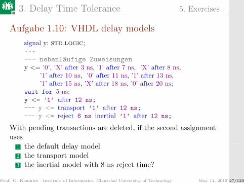
Aufgabe 1.10: VHDL delay models
signal y: STD LOGIC;...
--- nebenlaufige Zuweisungeny <= ’0’, ’X’ after 3 ns, ’1’ after 7 ns, ’X’ after 8 ns,
’1’ after 10 ns, ’0’ after 11 ns, ’1’ after 13 ns,’1’ after 15 ns, ’X’ after 18 ns, ’0’ after 20 ns;
wait for 5 ns;y <= ’1’ after 12 ns;
--- y <= transport ’1’ after 12 ns;
--- y <= reject 8 ns inertial ’1’ after 12 ns;
With pending transactions are deleted, if the second assignmentuses
1 the default delay model2 the transport model3 the inertial model with 8 ns reject time?
Prof. G. Kemnitz · Institute of Informatics, Clausthal University of Technology May 14, 2012 27/129

3. Delay Time Tolerance 5. Exercises
Aufgabe 1.11: Run time analysis
--- Vereinbarungsteil der Entwurfseinheitsignal x: STD LOGIC VECTOR(4 downto 0):=”01011”;signal z: STD LOGIC VECTOR(4 downto 0);signal y: STD LOGIC;
--- Anweisungsteil der EntwurfseinheitG1: z(0) <= ’X’ after 4 ns, x(0) and x(1) after 8
ns;
G2: z(1) <= ’X’ after 5 ns, x(2) or x(3) after 6 ns;
G3: z(2) <= ’X’ after 3 ns, z(0) or z(1) after 6 ns;
G4: z(3) <= ’X’ after 4 ns, z(1) and x(3) after 7
ns;
G5: z(4) <= ’X’ after 3 ns, z(3) or x(4) after 5 ns;
G6: y <= ’X’ after 5 ns, z(2) or z(4) after 7 ns;
1 Draw the signal flow plan with hold and delay times.2 Calculate the hold and the delay time of the complete
circuit.Prof. G. Kemnitz · Institute of Informatics, Clausthal University of Technology May 14, 2012 28/129

4. Register
Register
Prof. G. Kemnitz · Institute of Informatics, Clausthal University of Technology May 14, 2012 29/129

4. Register
Period of validity and sampling
≥1&z3
z1z2
0
10
1z3
z4
0
1
1z1
z2 0
period of validity at the begin of the pathperiode of validity at the end of the pathtGE
tGA
th3, td3th1, td1
z4≥1
th2, td2
00
td3td1 td2 tGE
th2 th3tGA th1
1
period of validity a the output:
tGA = tGE +
3∑i=1
thi −3∑
i=1
tdi
decreases with the length of the processing chainbroadening of the period of validity ⇒ sampling (register)
Prof. G. Kemnitz · Institute of Informatics, Clausthal University of Technology May 14, 2012 30/129

4. Register 1. Sampling with Registers
Sampling with Registers
Prof. G. Kemnitz · Institute of Informatics, Clausthal University of Technology May 14, 2012 31/129

4. Register 1. Sampling with Registers
Sampling with Registers
ts, tn
tTyp tTypx
T
T
x
thrtdr
tn
w1w0
ts
w2
w2w1
x’
thr, tdr
x’
ts tn
register: samples input data with the active clock edge1, elsestorets set-up time, time input data must be stable before theactive clock edgetn input hold time, time, the input data mus be stable afterthe active clock edge; will be often neglectedthr, tdr hold and delay time of the registertTyp: data type, �STD LOGIC�, vector type of is, ...
1rising, falling edge or both
Prof. G. Kemnitz · Institute of Informatics, Clausthal University of Technology May 14, 2012 32/129

4. Register 1. Sampling with Registers
Clock Signal
ts, tn
tTyp tTypx
T
T
x
thrtdr
tn
w1w0
ts
w2
w2w1
x’
thr, tdr
x’
ts tn
Clocks are special signals, switching periodically between�0� and �1� and are used for time adjustment of data signaltransitions
modelled as ideal binary signals (without �X�)the delay tolerance region is described by the registerparametersclock signals must be exactly in time and glitch free; requirespecial circuitry
active clock edge: rising, falling, bothProf. G. Kemnitz · Institute of Informatics, Clausthal University of Technology May 14, 2012 33/129

4. Register 1. Sampling with Registers
Notation for sampled signals
Sampling is a basic function of digital circuits; definition of anotation:
the signal sampled by a signal x will be named x+ (followingstate) (in VHDL x next)
the sampled signal of x will be called x’, the sampled signalof x’ will be called x” etc. (in VHDL x del, x del2 etc.)
(x next) (x del) (x del2)
x+ x x’ x”
T
Prof. G. Kemnitz · Institute of Informatics, Clausthal University of Technology May 14, 2012 34/129

4. Register 2. VHDL sampling process
VHDL sampling process
Prof. G. Kemnitz · Institute of Informatics, Clausthal University of Technology May 14, 2012 35/129

4. Register 2. VHDL sampling process
VHDL sampling process
behaviour of a sampling process
sampling process: process(T)
begin
if active clock edge then
output signal <= invalid after th,
input value after td;
check input setup time
check input hold time
end if;
end process;
additional required description means:
case distinctioncheck for clock edges (signal attribute)instructions to control input setup and hold conditions
Prof. G. Kemnitz · Institute of Informatics, Clausthal University of Technology May 14, 2012 36/129

4. Register 2. VHDL sampling process
signal attribute, description means to check additional signalfeatures:
signal s: tTyp;
constant t: DELAY LENGTH;
s’EVENT → BOOLEAN True, if the process has beenwaked-up by a transition of s
s’STABLE(t) → BOOLEAN True, true if there was no transitionsince time t
s’LAST EVENT →DELAY LENGTH
time since the last transition
s’LAST VALUE → tTyp value before the last transition of s
s’DELAYED(t) → tTyp the by t delayed signal of s
. . .
Prof. G. Kemnitz · Institute of Informatics, Clausthal University of Technology May 14, 2012 37/129

4. Register 2. VHDL sampling process
functions to check, whether a process was awakened be anactive edge (Package IEEE.STD LOGIC 1164):
function RISING EDGE(signal T: STD LOGIC) return BOOLEAN isbeginreturn T’EVENT and T=’1’;
end function;
function FALLING EDGE(signal T: STD LOGIC) return BOOLEAN isbeginreturn T’EVENT and T=’0’;
end function;
control input setup and hold conditions:
s’STABLE(t); s’LAST EVENT
binary case distinction for control flow:
if b then
{sequential statement;}
end if;
(b – condition of type BOOLEAN, e.g. �RISING EDGE(T)�Prof. G. Kemnitz · Institute of Informatics, Clausthal University of Technology May 14, 2012 38/129
4. Register 2. VHDL sampling process
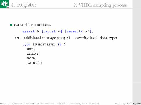
control instructions:
assert b [report m ] [severity sl ];
( m – additional message text; sl – severity level; data type:
type SEVERITY LEVEL is (
NOTE,
WARNING,
ERROR,
FAILURE);
Prof. G. Kemnitz · Institute of Informatics, Clausthal University of Technology May 14, 2012 39/129

4. Register 2. VHDL sampling process
Simple register modeltdr
x
y
T
w1 w3
w0 w1 w2
td
w2
ytTyptTyp
x
Tsignal T: STD LOGIC;
signal x, y: tTyp;
constant tdr: DELAY LENGTH:=...;
...
process(T)
begin
if RISING EDGE(T) then
y <= x after tdr;
end if;
end process;
process with only the clock in the sensitivity listoutput assignment only when a rising edgeRISING EDGE(T) ⇒ �T’EVENT and T=’1’�; if the processawakens �T’EVENT� is �TRUE�; except when the simulationstarts
Prof. G. Kemnitz · Institute of Informatics, Clausthal University of Technology May 14, 2012 40/129

4. Register 2. VHDL sampling process
A complete model ts, tn
tn
ts
sample windowinvalid
T
x
thrtdr
tn
w1w0
ts
w2
w2w1
T
x
thr, tdr
x’tTyp tTyp
x’
signal valuewi
register parameter:
signals:
input signalclock
xT
x’ (x del) sampled(output) signal
setup timeinput hold time(output) hold timedelay timetdr
thr
type data signaltTyp
ts tn
process(T)beginif RISING EDGE(T) thenif x’LAST EVENT>ts theny<= invalid after thr, x after tdr;wait for tn;
if x’LAST EVENT<tn theny <= invalid;
report "input hold cond. violated"
severity WARNING;
end if;elsey <= invalid after thr;
report "setup cond. violated"
severity WARNING;
end if;end if;
end process;Prof. G. Kemnitz · Institute of Informatics, Clausthal University of Technology May 14, 2012 41/129

4. Register 2. VHDL sampling process
No input hold time check (tn = 0) and warnings
process(T)beginif rising edge(T) thenif x’last event>ts theny <= invalid after thr, x after tdr;
elsey <= invalid after thr;
end if;end if;
end process;
This will be the simulation model of a register generally usein the following.
Prof. G. Kemnitz · Institute of Informatics, Clausthal University of Technology May 14, 2012 42/129

4. Register 3. Processing + Sampling
Processing + Sampling
Prof. G. Kemnitz · Institute of Informatics, Clausthal University of Technology May 14, 2012 43/129
4. Register 3. Processing + Sampling
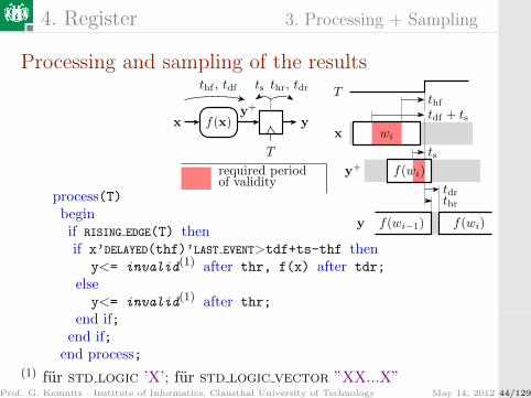
Processing and sampling of the results
ts
ts
required periodof validity
T
x
y
f(x)x
thf , tdf
wi
thftdf + ts
f(wi)
f(wi)f(wi−1)
tdrthr
T
thr, tdr
yy+
y+
process(T)beginif RISING EDGE(T) thenif x’DELAYED(thf)’LAST EVENT>tdf+ts-thf then
y<= invalid(1) after thr, f(x) after tdr;
elsey<= invalid(1) after thr;
end if;end if;
end process;(1) fur STD LOGIC ’X’; fur STD LOGIC VECTOR ”XX...X”
Prof. G. Kemnitz · Institute of Informatics, Clausthal University of Technology May 14, 2012 44/129

4. Register 3. Processing + Sampling
Processing of sampled signals
ts
ts
y
T
x
f(wi)f(wi−1)
T
thr, tdr
f(x)
thf , tdf
y
wiwi−1
thftdf
tdfthf
x’x
x’
wi
process(T)beginif RISING EDGE(T) thenif x’LAST EVENT>ts theny<= invalid after thr+thf,
f(x) after tdr+tdf;
elsey<= invalid after thr+thf;
end if;end if;
end process;
Prof. G. Kemnitz · Institute of Informatics, Clausthal University of Technology May 14, 2012 45/129

4. Register 4. Register transfer function
Register transfer function
Prof. G. Kemnitz · Institute of Informatics, Clausthal University of Technology May 14, 2012 46/129
4. Register 4. Register transfer function
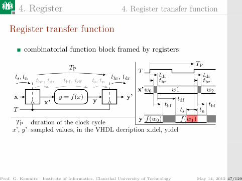
Register transfer function
combinatorial function block framed by registers
thr, tdrthr, tdr
x’, y’TP
sampled values, in the VHDL decription x del, y del
y
TP
w2
tdf
tdrthr
tdrthr
w1x’
thfthftn
y = f(x)
ts, tn
x y’
T
TP
ts, tn
x’ y
ts
thf , tdf
T
duration of the clock cyclef(w1)f(w0)
w0
Prof. G. Kemnitz · Institute of Informatics, Clausthal University of Technology May 14, 2012 47/129

4. Register 4. Register transfer function
thr, tdrthr, tdr
x’, y’TP
sampled values, in the VHDL decription x del, y del
y
TP
w2
tdf
tdrthr
tdrthr
w1x’
thfthftn
y = f(x)
ts, tn
x y’
T
TP
ts, tn
x’ y
ts
thf , tdf
T
duration of the clock cyclef(w1)f(w0)
w0
Requirements to sample valid output values
TP ≥ TPmin = tdr + tdf + ts
tn ≤ tnmax = thr + thf
Both requirements can be checked with a run time analysis(befor simulation)Simulation model can be greatly simplified
Prof. G. Kemnitz · Institute of Informatics, Clausthal University of Technology May 14, 2012 48/129

4. Register 4. Register transfer function
thr, tdr
f(...)
TP
yx’x
T
ts, tn
y’
Processing: process(T):
begin
if RISING EDGE(T) thenif x’LAST EVENT>ts thenx del <= x; else x <= invalid ;
end if;
y del <= invalid after th, f(x del) after td;
end if;
end process;
Simplification to multiple processest
undelayed assignment to x’ (x del)no check of setup conditions for y
Prof. G. Kemnitz · Institute of Informatics, Clausthal University of Technology May 14, 2012 49/129

4. Register 5. Clock skew
Clock skew
Prof. G. Kemnitz · Institute of Informatics, Clausthal University of Technology May 14, 2012 50/129

4. Register 5. Clock skew
Clock skew
sampling window
ts
t∆T12
yf(x’)
x′ y′
ts, tn
delayT2T1
x
thr, tdr
a)
sampling edge of input register
sampling edge of output register0
t∆T12
T1
T2
y
b)
TP
tdr
tdf
thr
thf
x′
thf , tdf
t
tn
Clock skew t∆T12: time offset between active clock edgesbetween input and output registersintended to increase the max. clock frequencyunintended by different delays
Prof. G. Kemnitz · Institute of Informatics, Clausthal University of Technology May 14, 2012 51/129

4. Register 5. Clock skew
sampling window
ts
t∆T12
yf(x’)
x′ y′
ts, tn
delayT2T1
x
thr, tdr
a)
sampling edge of input register
sampling edge of output register0
t∆T12
T1
T2
y
b)
TP
tdr
tdf
thr
thf
x′
thf , tdf
t
tn
Requirements for correct sampling:
tdr + tdf + ts ≤ TP + t∆T12
thr + thf ≥ tn + t∆T12
Prof. G. Kemnitz · Institute of Informatics, Clausthal University of Technology May 14, 2012 52/129

4. Register 5. Clock skew
Requirements for correct sampling:
tdr + tdf + ts ≤ TP + t∆T12
thr + thf ≥ tn + t∆T12
Maximum allowed clock skew:
t∆T12 ≤ thr + thf − tnMaximum allowed clock frequency:
fT ≤1
tdr + tdf + ts +−tn − (thr + thf)
Reciprocal value of the difference of the sum of the delay,the input hold, the setup and the output hold time.Circuits with a large hold time may be clocked faster withan appropriate clock skew then without
Prof. G. Kemnitz · Institute of Informatics, Clausthal University of Technology May 14, 2012 53/129

4. Register 5. Clock skew
Summary
Calculation results must be sampled within their periods ofvality by registers.Registers are discribed by sampling processes. In a samplingprocess only the clock is in the sensitivity list. Samplingwith the active clock edge. Setup or input hold conditionviolations invalidate register data.The description of the the combinatirial circuit before orafter the register may include in the sampling processes;simplify simulation.Framing by an input and an output register; timingcondition check by run time analysis; highly simplifiedsimulation model.
Prof. G. Kemnitz · Institute of Informatics, Clausthal University of Technology May 14, 2012 54/129

4. Register 6. Exercises
Exercises
Prof. G. Kemnitz · Institute of Informatics, Clausthal University of Technology May 14, 2012 55/129

4. Register 6. Exercises
Aufgabe 1.12: Desciption by a sampling process
thr, tdr
y+
ts
sampling windowinvalid
t3t4
t5
x1x0
y+
y
t6t7
t1t2
x2
T
a)
G1G2
& y
TReg
=1x0
x1
x2
th1, td1 th2, td2
b)
signal x0, x1, x2, y next, T, y: STD LOGIC;
Describe t1 to t7 as funcions of the values of th.., td... etc.Describe the whole circuit as a sampling process
Prof. G. Kemnitz · Institute of Informatics, Clausthal University of Technology May 14, 2012 56/129

4. Register 6. Exercises
Aufgabe 1.13: Register transfer function
x+ 1
xn−1
0
1
n
nn
x
nn
y+
tdr = 1ns
T
td1 = 0,5 ns td2 = n · 1 ns td3 = 2nsts = 0,5 ns
Determin:
maximum allowed clock frequency as a function of the bitwidth n?maximum allowed clock frequency for n = 16?
Prof. G. Kemnitz · Institute of Informatics, Clausthal University of Technology May 14, 2012 57/129

4. Register 6. Exercises
Aufgabe 1.14: Clock skew
thr = 0nstdr = 1ns
clock 1
x y
clock 2
y = f(x)
thf = 5nstdf = 11ns
tn = 0ts = 2ns
In which interval of time the clock skew has to be, so that for aclock frequncy fClk = 100 MHz the setup an the input holdconditions are met?
Prof. G. Kemnitz · Institute of Informatics, Clausthal University of Technology May 14, 2012 58/129

5. Asynchronous input
Asynchronous input
Prof. G. Kemnitz · Institute of Informatics, Clausthal University of Technology May 14, 2012 59/129

5. Asynchronous input
asynchronous: �without synchronisation�
the time delay between input change and the active clockedge is a transactions is a uniformly distributed randomvariable in the range:
txT ∈ {0, TP}
also asyncronous signals may only be evaluated within theirperiods of vality
special circuit solutions and VHDL descriptions are required
Prof. G. Kemnitz · Institute of Informatics, Clausthal University of Technology May 14, 2012 60/129

5. Asynchronous input 1. Sampling a single bit
Sampling a single bit
Prof. G. Kemnitz · Institute of Informatics, Clausthal University of Technology May 14, 2012 61/129

5. Asynchronous input 1. Sampling a single bit
Sampling of binary input signals
a single bit has, even if invalid during the sampling period,has the sampling value �0� or �1�; sampled signals are freeof glitches and stable during the clock period
T
x
x’
x′x
ts thr, tdr
T
ts ts ts ts
txT TP txT
tdrthr
tdrthr
tdrthr
tdrthr
Prof. G. Kemnitz · Institute of Informatics, Clausthal University of Technology May 14, 2012 62/129

5. Asynchronous input 1. Sampling a single bit
Design error: Processing of unsampled inputs
x
y
y′
a a′
T
x f(..)y
th, td
w1 w2
f(w1, 1) f(w2, 1)f(w1, 0)
f(w0, 0) XX f(w2, 1)
y′
ts th
ts
ththtdtd td
a
T
a
T
(processed) asynchronous inputs are withe a sertainprobability invalid during the sample periodthe sampled value of �invalid� is a random value ina′ ∈ {0, 1}n, mostly wrong, often anallowed, unpredictablebehaviourWorkaround: additional bitwise sampling of the asyncronousinput
Prof. G. Kemnitz · Institute of Informatics, Clausthal University of Technology May 14, 2012 63/129

5. Asynchronous input 2. Switch de-bouncing
Switch de-bouncing
Prof. G. Kemnitz · Institute of Informatics, Clausthal University of Technology May 14, 2012 64/129

5. Asynchronous input 2. Switch de-bouncing
De-bouncing of signals from switches and keys
typ. 1 bit input element: mechanical switch or keyBouncing: multiple on and off by mechanical vibrationsde-bouncing: sampling with a period larger than thebouncing timeEdge detection: sampling twice, check for difference
&
circuit to detectfalling edges
tP
tPr
1011 00 01 11
T
x
x’
x”
x”x’
x”x’y
x
T
tPr maximum bouncing time
sample periodtP > tPr
Take care, without unreliable sampling!
Prof. G. Kemnitz · Institute of Informatics, Clausthal University of Technology May 14, 2012 65/129

5. Asynchronous input 2. Switch de-bouncing
x
Tx’ x”
y&
th, td
y’
(clock)
signal T, x, x del, x del2, y:
STD LOGIC;
...
process(T)beginif RISING EDGE(T) then
if x=’1’ then x del<=’1’;else ’0’; end if;x del2 <= x del;
end if;end process;y <= ’X’ after th not x del and x del2 after td;
Sampling x: �’1’7→’1’, sonst 7→’0’� (template for�sampled value∈ {0, 1}combinatorial output, shortly invalid after each active clockedge; may be glitchesto use y as a clock, sample again
Prof. G. Kemnitz · Institute of Informatics, Clausthal University of Technology May 14, 2012 66/129

5. Asynchronous input 3. Asynch. initialization
Asynch. initialization
Prof. G. Kemnitz · Institute of Informatics, Clausthal University of Technology May 14, 2012 67/129

5. Asynchronous input 3. Asynch. initialization
Register with initialization input
I
x yx
I
T
signal x, y: tTyp;
signal T, I: STD LOGIC;
constant aw: tTyp:=...;
...
process(T, I)
beginif I=’1’ theny <= aw;
elsif RISING EDGE(T) theny <= x;
end if;end process;
register stage before initialization ”UU...U”(uninitialized/invalid)�aw� any valid value
Prof. G. Kemnitz · Institute of Informatics, Clausthal University of Technology May 14, 2012 68/129

5. Asynchronous input 3. Asynch. initialization
Potential malfunction
initialization pulse to short
01
01
w1 w2w0
w1 w2
T
x′x
I
f()
tsthf , tdfthr, tdr
yx’I
x
I
x
T≪ TP
y’
Even if the input register is initialized correctly, duration istto short, in witch the initial value is stable at the registeroutput. So the subsequent register may sample an invalidsignal.
Prof. G. Kemnitz · Institute of Informatics, Clausthal University of Technology May 14, 2012 69/129

5. Asynchronous input 3. Asynch. initialization
Register of master-slave flipflops:
master takes over before the active clock edge
slave takes over after the active clock edge
I initialization of the slave
01
01
01
01
w2w1w0
w2w1
T
I
x
x′
in the slave phase end of the slave phasedeactivation of I at thedeactivation of I
≪ TP
w0
w1 w2
T
I
x
x′ w2
invalid instead of w1
Prof. G. Kemnitz · Institute of Informatics, Clausthal University of Technology May 14, 2012 70/129

5. Asynchronous input 3. Asynch. initialization
Robust initialization
≥1
T
I
button
sampling
UVreset
reset circuitpower-on
signal T, I, I POR,
I Tast: STD LOGIC;
...
I POR <= ’1’, ’0’
after 1 ms;
process(T)
begin
if RISING EDGE(T) then
if I POR=’0’ or I Tast=’0’ then I<=’1’;else I<=’0’;end if;
end if;
end process;
power-on reset: after applying voltage active fortPOR ≈ R · Csampling to align to the active clock edge
Prof. G. Kemnitz · Institute of Informatics, Clausthal University of Technology May 14, 2012 71/129

5. Asynchronous input 4. Parallel interface
Parallel interface
Prof. G. Kemnitz · Institute of Informatics, Clausthal University of Technology May 14, 2012 72/129

5. Asynchronous input 4. Parallel interface
Asynchronous parallel interface
the receiver of asynchronous parallel data need additionalinformation about the period of validity, e.g. the clock of thetransmitterin the example x should be valid from each edge of Tx for aduration of tg
xw1 w2 w3 w4 w5
G
G
Tx’Tx
=1
x’
sampled input signal
send clockasynchronous input signalx
Tx
Gx’
validation signal for x’
T
T
Tx”
TPtg
w2w1w0 w3 w4 w5
w0
system clock
x
Tx
T
x’
Tx’
Tx”
Prof. G. Kemnitz · Institute of Informatics, Clausthal University of Technology May 14, 2012 73/129

5. Asynchronous input 4. Parallel interface
xw1 w2 w3 w4 w5
G
G
Tx’Tx
=1
x’
sampled input signal
send clockasynchronous input signalx
Tx
Gx’
validation signal for x’
T
T
Tx”
TPtg
w2w1w0 w3 w4 w5
w0
system clock
x
Tx
T
x’
Tx’
Tx”
all input signals sampled with a period TP < tgthe clock is sampled twicesampled data are valid if the sampled transmitter clockdiffers from the twice sampled
Prof. G. Kemnitz · Institute of Informatics, Clausthal University of Technology May 14, 2012 74/129

5. Asynchronous input 4. Parallel interface
x
SYNC y
G
x
Tx
symbol
f(...)Tx’ =1
TTx
x’
G
synchronization circuit
signal T, Tx, Tx del, Tx del2, G: STD LOGIC;
signal x, y: STD LOGIC VECTOR(...);
...process(T)beginif RISING EDGE(T) theny<= x;
if Tx=’1’ then tx del <= ’1’;
else tx del <= ’0’;
end if;tx del2 <= Tx del;
end if;end process;G <= Tx del xor Tx del2;
Prof. G. Kemnitz · Institute of Informatics, Clausthal University of Technology May 14, 2012 75/129

5. Asynchronous input 4. Parallel interface
Summary
sample asyncronous signals before processing
in addion de-bounce signals from mechanical switches;sample period larger bouncing time
sample asynchronous initialization signals
asynchronous parallel input signals needs additional validityinformation; sampling by a synchronization circuit
forgotten sampling causes non-recurring malfunctions;difficult to locate; reduced reliability
Prof. G. Kemnitz · Institute of Informatics, Clausthal University of Technology May 14, 2012 76/129

5. Asynchronous input 5. Exercises
Exercises
Prof. G. Kemnitz · Institute of Informatics, Clausthal University of Technology May 14, 2012 77/129

5. Asynchronous input 5. Exercises
Aufgabe 1.15: Adding up asynchronous input
UV power supply
adder
(signal value ’1’)
(signal value ’0’)ground
· · ·
T
+
UV
xn−1
x1
x0+
Under which operational conditions the circuit may havenon-recurring malfunctions?
How the circuit has to be changed to work reliable?
Prof. G. Kemnitz · Institute of Informatics, Clausthal University of Technology May 14, 2012 78/129
5. Asynchronous input 5. Exercises
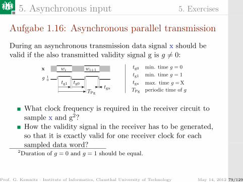
Aufgabe 1.16: Asynchronous parallel transmission
During an asynchronous transmission data signal x should bevalid if the also transmitted validity signal g is g 6= 0:
0g
x wi+1wi
tg1
TPg
tgxtg0
1
periodic time of gTPg
tgx
min. time g = 1tg1
min. time g = 0tg0
max. time g =X
What clock frequency is required in the receiver circuit tosample x and g2?How the validity signal in the receiver has to be generated,so that it is exactly valid for one receiver clock for eachsampled data word?
2Duration of g = 0 and g = 1 should be equal.
Prof. G. Kemnitz · Institute of Informatics, Clausthal University of Technology May 14, 2012 79/129

5. Asynchronous input 5. Exercises
Aufgabe 1.17: Hand clock
Design a circuit with an input button x, en input clock T(fT = 50 MHz) and internal clock divider to produce ade-bounced hand clock without glitches:
entity HandClock isport(x: in std logic; -- input signal from button
T: in std logic; -- input clock, 50MHz
Tout: out std logic); -- hand clock, de-bounced, no glitches
end entity;
Maximum bouncing time 20 msMinimum activation time 100 ms.Divider proportion for the clock should be a power of two.
Prof. G. Kemnitz · Institute of Informatics, Clausthal University of Technology May 14, 2012 80/129

5. Asynchronous input 5. Exercises
1 What is the advantage of a power of two for the dividerproportion? (Note, the circuit has no initialization input.)
2 What values are allowed for the divider proportion?
3 Draw the whole circuit with the clock divider as a black box.
4 Describe the complete circuit in VHDL.
Prof. G. Kemnitz · Institute of Informatics, Clausthal University of Technology May 14, 2012 81/129

6. Sequential circuit
Sequential circuit
Prof. G. Kemnitz · Institute of Informatics, Clausthal University of Technology May 14, 2012 82/129

6. Sequential circuit
Sequential circuit
I
10I1
0
state register
optinal input and output register
Ix
y’
y
Y0 Y1
Y0 Y1 Y2
fs(x, s)
fy(x, s)
x
y’
s
x+
I+y
T
th, td
S0
X1
S1
X2
S1
tdth
S2
s
s+
x X0
S0
T
combinatorial circuit
value validpoint of sample time
sequential: in consecutive stepsCalculation of the circuit outputs in multiple time stepscombinatorial circuit + registers for sampling and storing
Prof. G. Kemnitz · Institute of Informatics, Clausthal University of Technology May 14, 2012 83/129

6. Sequential circuit 1. Finite state machine
Finite state machine
Prof. G. Kemnitz · Institute of Informatics, Clausthal University of Technology May 14, 2012 84/129

6. Sequential circuit 1. Finite state machine
Finite state machine
general function model to describe sequential operations; definingvalue ranges as symbol sets:
range of input values: Σ = {E1, E2, . . .}range of states: S = {Z1, Z2, . . .} (one is initial state)range of output values: Π = {A1, A2, . . .}
and operation as mappings:
transfer function: fs : S × Σ→ Soutput function: fa : S × Σ→ Π
Digital circuits as finite state machines:
symbols 7→ bit vectors; input, output 7→ signalsstate 7→ register; transfer and output function 7→combinatorial circuitstate transition synchronized to a clockinitial state = initialing value of the state register
Prof. G. Kemnitz · Institute of Informatics, Clausthal University of Technology May 14, 2012 85/129

6. Sequential circuit 1. Finite state machine
Description by a state graph
transition conditionstate transition
name of the statestate
output
Z3
AZ1
Z1
AK3.1
E1.1
Z2
AZ2
AZ2
AK2.1
AK1.1
AK2.2
AK2.1
E2.1
E2.2E1.2
E3.1
inital statesymbol for the
output depends only upon the state / assigned to states /the same for all outgoing edges 7→ Moore automatonoutput also depends on input / assigned to the outgoingedges 7→ Mealy automaton
Prof. G. Kemnitz · Institute of Informatics, Clausthal University of Technology May 14, 2012 86/129

6. Sequential circuit 1. Finite state machine
Up-/down counter as a Mealy automaton
states
R/N
A B
CD
V/L
R/LV/KR/K
V/M
R/M
V/N
H/L
H/M
H/K
H/N
Π = {K,L,M,N}S = {A,B,C,D}Σ = {H,V,R}
initial state
range of state values
range of output values
x/y
input value
output value
range of input values
Meanings of the input values: H – stop; V – up; R – down
Prof. G. Kemnitz · Institute of Informatics, Clausthal University of Technology May 14, 2012 87/129

6. Sequential circuit 1. Finite state machine
⇒ ⇒
BA
CD
V
BCDA
H
BA
CD
R
BA
C
D
V H R
KLMNK
LMN
KLM
N 0010
1011
KLMN
1011
CD
0010
VHR
000110 01
00
1011
00011011
000110
11
00
011011
00 01 10
00011011
000110
11
00
011011
00 01 10
s+ = fs(x, s)
s x :
AB
s x :
s+ = fs(x, s)
codingstate
function with symbolic valuesstate transition and output
function with bitvectorsstate transition and output
y = fa(x, s) y = fa(x, s)
state graph: obviously well suited to specify target functions
extractable tabular state transfer and output function
state coding: assigning bit vectors to symbols
translation to a presentation with bit vectors
Prof. G. Kemnitz · Institute of Informatics, Clausthal University of Technology May 14, 2012 88/129

6. Sequential circuit 1. Finite state machine
Up-/down counter as a Moore automaton
BA
CD
V
BCDA
H
BA
CD
R
BA
C
D KLMN
s
y
state
output value
input value
{K,L,M,N} output set{A,B,C,D}{H,V,R}
state setinput set
RV
V
R
V
RV R
D
A B
C
K L
MN
H H
H
ba
H
s x :
s+ = fs(x, s) y = fy(s)
x
fs(...)fa(...)
xss+
y outputtransfer functionoutput function
next stateactual stateinput
the output depends on the state
Prof. G. Kemnitz · Institute of Informatics, Clausthal University of Technology May 14, 2012 89/129

6. Sequential circuit 1. Finite state machine
Autonomous automaton
no input; one outgoing edge per state
A B C D
E G HFb)
A B C D
EFGHa)
a) cyclical automaton; example application clock dividerb) without cycle but a final state; example initialization run
If no outputs are assigned in the state graph the state is theoutput.
Prof. G. Kemnitz · Institute of Informatics, Clausthal University of Technology May 14, 2012 90/129

6. Sequential circuit 2. Automaton ⇒ VHDL
Automaton ⇒ VHDL
Prof. G. Kemnitz · Institute of Informatics, Clausthal University of Technology May 14, 2012 91/129

6. Sequential circuit 2. Automaton ⇒ VHDL
Circuit structure of automatons
I
10I1
0
state register
optinal input and output register
Ix
y’
y
Y0 Y1
Y0 Y1 Y2
fs(x, s)
fy(x, s)
x
y’
s
x+
I+y
T
th, td
S0
X1
S1
X2
S1
tdth
S2
s
s+
x X0
S0
T
combinatorial circuit
value validpoint of sample time
the input and the initialization signal must be aligned to theclock
Prof. G. Kemnitz · Institute of Informatics, Clausthal University of Technology May 14, 2012 92/129

6. Sequential circuit 2. Automaton ⇒ VHDL
I Ixfs(x, s)
fy(x, s)
x
y’
s
x+
I+y
T
th, td
the optional input and output register are generally notcounted as part of the automatoninitializing the state register ⇒ switching to the initial statestate register + transfer function ⇒ sampling process withinitialization (T , I in the sensitivity list)output function without sampling ⇒ combinatorial process(x, s in the sensitivity list)
Prof. G. Kemnitz · Institute of Informatics, Clausthal University of Technology May 14, 2012 93/129

6. Sequential circuit 2. Automaton ⇒ VHDL
VHDL case instruction to describe tabularfunctions
} =>{ |WertWert
{instruction instruction}A0 A1 An
. . .
. . .
w0 w1
selse
case expression
when
{when
} =>{ |Wertvalue
end case
=>
;{instruction }]]
{instruction instruction}} A1w1
A0
w0
value to selectsvalues to bee selected iinstruction sequence iAi
An[[when others
instruction wi
is s
the transfer an the output functions derived from the stategraph best be described by case and if statements, e.g.:
case state is
when Zi => if input=... then state <= Zj; ...
Prof. G. Kemnitz · Institute of Informatics, Clausthal University of Technology May 14, 2012 94/129

6. Sequential circuit 2. Automaton ⇒ VHDL
Example of a mealy automaton
circuit structure
fs xI
00
0110
0/1
1/0
1/1
1/10/0
state graph
0/0 s+ ysx
I
T T
fy
part of the automatonnecessary, but not
input range: {0, 1} ⇒ bitRange oft states: {00, 01, 10} ⇒ 2 bit vectoroutput range: {0, 1} ⇒ bit
signal x, y, T, I: STD LOGIC;
signal s: STD LOGIC VECTOR(1 downto 0);
Prof. G. Kemnitz · Institute of Informatics, Clausthal University of Technology May 14, 2012 95/129

6. Sequential circuit 2. Automaton ⇒ VHDL
Transfer function in a sample process
s+
Ifsx
xI
T
s
00
0110
0/1
1/01/10/0
1/1
0/0
process(I, T)
variable sx: STD LOGIC VECTOR(2 downto 0);
beginif I=’1’ thens <= "00";
elsif RISING EDGE(T) thensx := s & x;
case sx iswhen "00"&’0’ | "10"&’0’ => s <= "00";
when "01"&’0’ | "00"&’1’ => s <= "01";
when "10"&’1’ | "01"&’1’ => s <= "10";
when others => s <= "XX";
end case;end if;
end process;
Selection expression: concatenation of state and inputProf. G. Kemnitz · Institute of Informatics, Clausthal University of Technology May 14, 2012 96/129

6. Sequential circuit 2. Automaton ⇒ VHDL
Output function as combinatorial process
00
0110
0/1
1/01/10/0
0/0
1/1process(x, s)
variable sx: STD LOGIC VECTOR(2 downto 0);
beginsx <= s & x;
case sx iswhen "00"&’1’ | "01"&’0’ | "10"&’0’ => y <= ’0’;
when "00"&’0’ | "01"&’1’ | "10"&’1’ => y <= ’1’;
when others => y <= ’X’;
end case;end process;
The selection expression is again a concatenation of the state andthe input.
Prof. G. Kemnitz · Institute of Informatics, Clausthal University of Technology May 14, 2012 97/129

6. Sequential circuit 2. Automaton ⇒ VHDL
Example Moore automaton
process(s)begincase s iswhen "01" => y <= ’0’;
when "00"|"10" => y <= ’1’;
when others => s <= ’X’;
end case;end process; x
I
T
001 1
100
011001
1
0
s+ s
I
T
xy
fyfs
input, state and output range and transfer function are thesame as in the example beforethe output only depends upon the state
Prof. G. Kemnitz · Institute of Informatics, Clausthal University of Technology May 14, 2012 98/129

6. Sequential circuit 2. Automaton ⇒ VHDL
Autonomous Automaton, example Johnsoncounter
0000
1000 1100 1110 1111
011100110001 s0 s1 s2 s3
II+
T
x
I I I
x x x
shift register, that alternating filled first with ones and thanwith zeroscycle length 2 · n (n – number of register bits)very low register register delay; high clock frequencyapplication as fast prescaler, e.g. to measure frequencies inthe GHz range
Prof. G. Kemnitz · Institute of Informatics, Clausthal University of Technology May 14, 2012 99/129

6. Sequential circuit 2. Automaton ⇒ VHDL
0000
1000 1100 1110 1111
011100110001 s0 s1 s2 s3
II+
T
x
I I I
x x x
signal T, I: STD LOGIC;
signal s: STD LOGIC VECTOR(3 downto 0);
...
process(I, T)
beginif I=’1’ then s <= "0000";
elsif RISING EDGE(T) thens <= s(2 downto 0) & (not s(3));
end if;end process;
For some automatons the transfer and the output functioncan be described much simpler than with case and ifstatements.
Prof. G. Kemnitz · Institute of Informatics, Clausthal University of Technology May 14, 2012 100/129

6. Sequential circuit 3. System crash
System crash
Prof. G. Kemnitz · Institute of Informatics, Clausthal University of Technology May 14, 2012 101/129

6. Sequential circuit 3. System crash
Illegal states and system crash
n memory elements ⇒ 2n states; not all are usedWhat happens in the unused (illegal) states?
Example 4 Bit Johnson counter:
0100
1011
mal-function
wayback
s3s2s1s0
correct function operation after crash
0000
111111101100
1000
0001 0011
0111 0101
00101001
01101101
1010no
Automaton cycles illegal statestill reinitialization no reasonable behavior⇒ crash
Prof. G. Kemnitz · Institute of Informatics, Clausthal University of Technology May 14, 2012 102/129

6. Sequential circuit 3. System crash
Automated crash recovery
circuit for an automatic reinitialization
0000.0
1111.0
I
T
xs0
I
x
I
x
s1 s2
&
I+
s3
I
xI+r≥1
- - - -.1
illigal states Cycle of the legal states
transitions bymalfunctions
s3s2s1s0.I
0111.00011.00001.0
1110.01100.01000.01101.0
0101.01001.00100.0
1010.0 0110.0
0010.0
1011.0
adding the illegal states; defining edges to leave themIn the example a reset is performed automatically, if theJohnson counter reaches the state �1101� or �0101�.
Prof. G. Kemnitz · Institute of Informatics, Clausthal University of Technology May 14, 2012 103/129
6. Sequential circuit 3. System crash
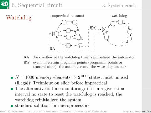
Watchdog
cyclic in certain progamm points (programm points ortransmissions), the automat resets the watchdog counter
supervised automat watchdog
RW
RA
RA
RW
An overflow of the watchdog timer reinitialized the automaton
N = 1000 memory elements ⇒ 21000 states, most unused(illegal); Technique on slide before impracticalThe alternative is time monitoring: if if in a given timeinterval no state to reset the watchdog is reached, thewatchdog reinitialized the systemstandard solution for microprocessors
Prof. G. Kemnitz · Institute of Informatics, Clausthal University of Technology May 14, 2012 104/129

6. Sequential circuit 4. Combination lock
Combination lock
Prof. G. Kemnitz · Institute of Informatics, Clausthal University of Technology May 14, 2012 105/129

6. Sequential circuit 4. Combination lock
Control design of a combination lock
Input sequence: reset + right number sequence ⇒ outputLED turns onInput sequence: reset + wrong number sequence ⇒ outputLED stays off
Design flow:
Circuit sketch, input elements, sampling register, clockcircuitry; transfer and output function as circuit blocks stillto designSpecification of the state graphState encoding (if not given input and output encoding)Description in VHDLSimulationSynthesis, ...
Prof. G. Kemnitz · Institute of Informatics, Clausthal University of Technology May 14, 2012 106/129

6. Sequential circuit 4. Combination lock
Circuit sketch
xI
&x xU
x+
x+m−1
fs
sfy
xU’
s+
y
TI+
x+0
UV
· · ·x+1
I
m number buttons + reset key; asynchronous de-bounced;sampling e.g. with TP ≈ 10 ms; �0� if pressedvalid input: sequence no key pressed - single key pressed;multiple key; multiple keys pressed should be handled in thesame way as wrong key pressedOutput LED + series resistor; on when y = 0Moore automaton (output assigned to the states)Reinitialization with the sampled reset value �0�
xU – AND instruction of the key signals; if no button ispressed during the sampling �1�, else �0�
Prof. G. Kemnitz · Institute of Informatics, Clausthal University of Technology May 14, 2012 107/129

6. Sequential circuit 4. Combination lock
Designing the state flow
1110∗ 0111∗ 1101∗
LED offZ2 Z3
LED onLED offZ0 Z1
LED off
LED offF
else∗ else∗else∗
∗ ∧(xU = 0) ∧ xU’= 1)
Acceptor automaton; Zi name of the state; i – number ofthe next secret keytransition condition: active clock edge ∧ xU = 0 (keypressed) ∧ xU’ (step before no key pressed) ∧s 6= F ∧ s 6= Z3
(not final state)correct number sequence 0-3-1 ⇒ input vector sequence1110-0111-1101 (m = 4 number keys)wrong input ⇒ error state FThe final states F and Z3 are left only by reinitialization.
Prof. G. Kemnitz · Institute of Informatics, Clausthal University of Technology May 14, 2012 108/129

6. Sequential circuit 4. Combination lock
Description in VHDL
xI
&x xU
x+
x+m−1
fs
sfy
xU’
s+
y
TI+
x+0
UV
· · ·x+1
I
signal T, I next, I, xu, xu del: STD LOGIC;
signal s: STD LOGIC VECTOR(2 downto 0);
signal x next, x: STD LOGIC VECTOR(3 downto 0);...
process(T) beginif RISING EDGE(T) thenx <= x next;
I <= I next;
xu del <= xu;
end if;end process;
xu <= x(0) and x(1) and x(2) and x(3);Prof. G. Kemnitz · Institute of Informatics, Clausthal University of Technology May 14, 2012 109/129

6. Sequential circuit 4. Combination lock
final states: 1- -
Z1
LED offLED offZ0 Z3
LED on
000
100010001
111
Z0
Z1
Z2
Z3
F
state coding
∗ ∧(xU = 0)∧xU’= 1)LED of
F
1110∗ 0111∗
else∗else∗
1101∗
else∗LED off
Z2
process(I, T)
variable v: STD LOGIC VECTOR(6 downto 0);
beginif I=’0’ thens <= "000";
elsif RISING EDGE(T) and xu=’0’
and xu del =’1’ and s(2)=’0’ thenv:= s & x del;
case v iswhen "000" & "1110" => s<="001";when "001" & "0111" => s<="010";when "010" & "1101" => s<="100";when others => s <= "111";
end case;end if;
end process;--- concurrent signal asignment to the output y
y<= not s(2) or s(1) or s(0);Prof. G. Kemnitz · Institute of Informatics, Clausthal University of Technology May 14, 2012 110/129
6. Sequential circuit 4. Combination lock
Summery
Circuit design using finite state machines:
sketch of the circuit with the Automaton as a Black-Box(creative)
specify operation by a state graph (creative)
translate description to VHDL (prescription like)
Prof. G. Kemnitz · Institute of Informatics, Clausthal University of Technology May 14, 2012 111/129

6. Sequential circuit 5. Operation graph
Operation graph
Prof. G. Kemnitz · Institute of Informatics, Clausthal University of Technology May 14, 2012 112/129

6. Sequential circuit 5. Operation graph
Operation graph
The number of states and edges in an state graph growexponentially with number of input and state bits.
How information can be structures better?As in a computer program:
also a operation graph, which controls data operationlimited range of operation: add, count, logical bit operations...
Operation graph: extended state graph, that in additioncontrols Operation and checks operational results forconditional state transfer.
Definition of operands and operations to describe the targetfunction as a register transfer functionDescribing the operation flow as graph.
Even a single count operation may simplify the operation flowdramatically.
Prof. G. Kemnitz · Institute of Informatics, Clausthal University of Technology May 14, 2012 113/129

6. Sequential circuit 5. Operation graph
Triangle signal generator
000000010010
11101101
1111
0 15 30
y
step
autonomous automaton, which periodically cycles the 30statesstate space separable in counting direction (up, down) andcount value (�0000� to �1111�)the two unused state tuple (�0000�, down) and (�1111�,up) are illegalrequired operations: clr (initialize with �0000), inc (countup) and dec (count down)
Prof. G. Kemnitz · Institute of Informatics, Clausthal University of Technology May 14, 2012 114/129

6. Sequential circuit 5. Operation graph
+1
0000 y
operations of the count register
y
y
inc
dec
clr
−1
operation graph
0inc
1dec
y=1110
y=0001
clrI=1
elseelse
000000010010
11101101
1111
0 15 30
y
step
library Tuc;
use Tuc.Numeric Sim.all;...signal T, I, s: STD LOGIC;
signal y: tUnsigned(3 downto 0);...process(I, T)beginif I=’1’ thens <= ’0’; y <= ”0000”;
elsif RISING EDGE(T) thencase s iswhen ’0’ => y <= y +”1”;
if y=”1110” then s<=’1’; end if;when ’1’ => y <= y -”1”;
if y=”0001” then s<=’0’; end if;when others => y <= ”XXXX”;
end case;end if;
end process;
Prof. G. Kemnitz · Institute of Informatics, Clausthal University of Technology May 14, 2012 115/129

6. Sequential circuit 6. Quadrature encoder
Quadrature encoder
Prof. G. Kemnitz · Institute of Informatics, Clausthal University of Technology May 14, 2012 116/129

6. Sequential circuit 6. Quadrature encoder
Displacement measuring with quadrature encoder
forwardbackward
forward backward
1 2 30 44 5 3 2 1 0
a’
b’ b”
a”0000
0 0 000 1
10
000
111
0 10 01 1
111
000
1 01 10 0
111
111
1 11
10
0
b’a” b” a’
−1
−1+1
+1
+1−1
+1−1
ct
T
0
01
1b’
a’
ct
a
b
perforated disk at a wheel axle e.g. of a mobile robotduring turning ahead the signal a and during during turningback the signal b changes first
Prof. G. Kemnitz · Institute of Informatics, Clausthal University of Technology May 14, 2012 117/129

6. Sequential circuit 6. Quadrature encoder
forward backward
00000 0 0
00 110
000
111
0 10 01 1
111
000
1 01 10 0
111
111
1 11
10
0
b’a” b” a’
−1
−1+1
+1
+1−1
+1−1
ct
1 2 30 44 5 3 2 1 0
0
01
1b’
a’
ct
stop / don’t count: a”b” = a’b’illegal: a”b” = a’b’
rotation forward / count up
first a turns on (a”b”a’b’ = 0010)then b turns on (a”b”a’b’ = 1011)then a turns off (a”b”a’b’ = 1101)at last b turns off (a”b”a’b’ = 0100).
rotation backward / count down
first b turns on(a”b”a’b’ = 0001)then a turns on(a”b”a’b’ = 0111)then b turns off(a”b”a’b’ = 1110)at last a turns off(a”b”a’b’ = 1000)
transfer function:a”b” <= a’b’
Prof. G. Kemnitz · Institute of Informatics, Clausthal University of Technology May 14, 2012 118/129

6. Sequential circuit 6. Quadrature encoder
library Tuc; use Tuc.Numeric Sim.all;...signal T, I, I del: STD LOGIC;signal ab: STD LOGIC VECTOR(1 downto 0);signal ab del: STD LOGIC VECTOR(3 downto 0);
signal ct: tSigned(15 downto 0);
--- Abtastprozess ohne Initialisierung
process(T)beginif RISING EDGE(T) thenI del <= I;
ab del(1 downto 0) <= ab;
ab del(3 downto 2) <=ab del(1 downto 0);
end if;end process;
a’
b’ b”
a”a
b
T
Prof. G. Kemnitz · Institute of Informatics, Clausthal University of Technology May 14, 2012 119/129

6. Sequential circuit 6. Quadrature encoder
00000 0 0
00 110
000
111
0 10 01 1
111
000
1 01 10 0
111
111
1 11
10
0
b’a” b” a’
−1
−1+1
+1
+1−1
+1−1
ct
--- Zahlerprozess
process(I del, T)beginif I del=’1’ thenct <= ”0000000000000000”;
elsif RISING EDGE(T) thencase ab del iswhen ”0010” |”1011” |”1101” |”0100” => ct <= ct +”1”;when ”0001” |”0111” |”1110” |”1000” => ct <= ct -”1”;when ”0000” |”0101” |”1010” |”1111” => null;when others => ct <=”X...(16×X)...XX”;
end case;end if;
end process;
Prof. G. Kemnitz · Institute of Informatics, Clausthal University of Technology May 14, 2012 120/129

6. Sequential circuit 6. Quadrature encoder
Summary
functional specification as state graph; recipe likeimplementation in VHDL and further in a circuit
state ⇒ state register, sampling processinitial value ⇒ initial value of the state registertransfer and output function ⇒ sample or combinatorialprocess with case distinction on case and input
illegal states; danger to crash; typical error handlingreinitialization; reset button, watchdogcomplex functions with large input and state ranges
describing target function by an operation sequencespecification of operands and operations as register transferfunctionsoperation graphrecipe like mapping to VHDL
Prof. G. Kemnitz · Institute of Informatics, Clausthal University of Technology May 14, 2012 121/129
6. Sequential circuit 7. Exercises
Exercises
Prof. G. Kemnitz · Institute of Informatics, Clausthal University of Technology May 14, 2012 122/129

6. Sequential circuit 7. Exercises
Aufgabe 1.18: Feedback shift register
b)a)
x
I
x
I00
10
10
10
10
x
IT
y
s0 s1
T
x
I
s1s0
y
=1=1
Determine the next states s+1 s
+0 and the output value y for
each variation of the actual state s1s0 and the input value ofxdraw the state graphAdd the signal flow for s1s0 and y in the figure right.
Prof. G. Kemnitz · Institute of Informatics, Clausthal University of Technology May 14, 2012 123/129

6. Sequential circuit 7. Exercises
Aufgabe 1.19: Automaton
Z1
y<=’0’
y<=’1’
Z4
Z2
y<=’1’
x=’1’
x=’1’
x=’1’
y<=’0’
Z3
x=’0’x=’0’
x=’0’
x=’1’
x=’0’
symbolic state name Z1 Z2 Z3 Z4
assigned bit vector ”00” ”01” ”10” ”11”
state transition with the rising clock edgeinitialization with I=’1’
Prof. G. Kemnitz · Institute of Informatics, Clausthal University of Technology May 14, 2012 124/129

6. Sequential circuit 7. Exercises
1 Fill in the state transition table
input 0 1 0 1 0 1 0 1
state 00 00 01 01 10 10 11 11
next state
output
2 Drawing of the complete circuit (input sampling, stateregister, transfer function, output function)
3 How many memory elements are required?
4 Description in VHDL (entity + architecture).
Prof. G. Kemnitz · Institute of Informatics, Clausthal University of Technology May 14, 2012 125/129

6. Sequential circuit 7. Exercises
Aufgabe 1.20: Monitor for a transmitter signals
For a transmitter signal it has to be monitored, that thedifference ∆ between the number of transmitted ones minus thetransmitted zeros does not exceed the range of −3 to 3. In caseof violation error signal y should become active. Example waveform:
x 1 0 0 0 0 0 1 0 1 1 1 1 1 1 1 . . .
∆ 0 1 0 -1 -2 -3 -3 -2 -3 -2 -1 0 1 2 3 3
y 0 0 0 0 0 1 0 0 0 0 0 0 0 0 1 . . .
(x – input; ∆ – number of �0� minus number of �1�; y – errorsignal)
To do:
Draw state graphVHDL declaration + process description(s)
Prof. G. Kemnitz · Institute of Informatics, Clausthal University of Technology May 14, 2012 126/129

6. Sequential circuit 7. Exercises
Aufgabe 1.21: Clock divider
Design a clock divider with division factor 2 · n, which with eachn-th active input clock edge events the output clock. To do:
Draw the signal flow of the input and the output clock forn = 2.
Describe the target function withe an operation graph and acounter.
VHDL description. Parameter n should be declared as aconstant.
Hint: The data type of the counter signal may also be a numbertype (INTEGER, NATURAL or POSITIVE).
Prof. G. Kemnitz · Institute of Informatics, Clausthal University of Technology May 14, 2012 127/129

6. Sequential circuit 7. Exercises
Aufgabe 1.22: Morse receiver
4 6 8 102
A R I SP
0
1
0x
t in s
Morse signals consist of
short pulses (dot, tP = 200...300 ms) andlong pulses (dash, tS = 600...900 ms).
clock frequency: fT = 20 Hzbouncing time less than clock period.two low active input button
signal x: Morse signalsignal I: Initialization signal
Prof. G. Kemnitz · Institute of Informatics, Clausthal University of Technology May 14, 2012 128/129

6. Sequential circuit 7. Exercises
Three output bits, to be activated for one clock
signal p: after receiving a dotsignal s: after receiving a dashsignal err: after receiving a pulse of unallowed length
Draw complete circuit with buttons, sample registers, stateregisters and the transfer and the output function as blackbox .
Operation graph using a counter
VHDL description (only declaration of the date objects andthe processes)
Prof. G. Kemnitz · Institute of Informatics, Clausthal University of Technology May 14, 2012 129/129