design of embedded systems advanced...
TRANSCRIPT
EDA385
Design of Embedded Systems Advanced Course
DCC – Direct Current Control
2010-11-22
Jakob Hä[email protected]
Per Sö[email protected]

Abstract
Almost always when using some kind of electromagnetic device and you want to control the field strength, force or torque produced by it you will have to control the current driven through it. There are some different ways to achieve this. Since the load always is more or less inductive, switching power electronics gives great possibilities to control the current while the losses will remain small. The tricky part is to control the switches in the right way, and that is what direct current control (DCC) is about. DCC strives to keep the current ripple at a constant level, i.e. if the current rises above the upper allowed value the controller changes the switches to lower the current and if the current falls below the lower allowed value it changes them to increase the current.

Contents
1 Introducing theory.............................................................................................................................................................12 Changes since proposal.....................................................................................................................................................23 System overview................................................................................................................................................................34 Details on synthesized hardware.......................................................................................................................................4
4.1 CRC...........................................................................................................................................................................44.2 DCC-logic.................................................................................................................................................................44.3 Block diagram...........................................................................................................................................................64.4 Device occupancy for hardware................................................................................................................................6
5 Details on software............................................................................................................................................................75.1 The LYTMA-kernel..................................................................................................................................................75.2 Implementation of the LYTMA-kernel.....................................................................................................................75.3 Develop software using the LYTMA-kernel.............................................................................................................75.4 Vector........................................................................................................................................................................75.5 Hysteresis band.........................................................................................................................................................85.6 Serial communication...............................................................................................................................................8
5.6.1 Serial protocol..................................................................................................................................................85.6.2 Choice of error detecting method in serial communication.............................................................................85.6.3 Packet design....................................................................................................................................................85.6.4 Communication algorithm for computer and FPGA......................................................................................10
6 External hardware............................................................................................................................................................127 Simulator.........................................................................................................................................................................128 GUI..................................................................................................................................................................................139 Manual.............................................................................................................................................................................1510 Problems........................................................................................................................................................................1711 Lesson learned...............................................................................................................................................................1712 Contributions.................................................................................................................................................................1713 Sources...........................................................................................................................................................................18
1 Introducing theory
It is always attractive to use electricity to create force and movement since it is clean and has high efficiency. The conversion from electricity to force appends on electromagnetism where the force depends on the field strength. The field strength depends in a similar way on the current driven through the device, so even if you want to use the field it self or use it to create force in a permanent magnetized synchronous machine the most inner loop of the whole controller will be a current controller. Hence the performance of the current controller will determine the maximum performance of the whole system.
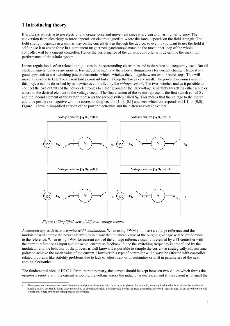
Linear regulation is often related to big losses in the surrounding electronics and is therefore not frequently used. But all electromagnetic devices are more or less inductive and have therefore a sluggishness for current change. Hence it is a good approach to use switching power electronics which switches the voltage between two or more steps. This will make it possible to keep the current fairly constant but still keep the losses very small. The power electronics used in this project can be described by two switches controlled by the voltage vector1. The two switches makes it possible to connect the two outputs of the power electronics to either ground or the DC-voltage separately by setting either a one or a zero in the desired element in the voltage vector. The first element of the vector represents the first switch called SA
and the second element of the vector represents the second switch called SB. This means that the voltage to the motor could be positive or negative with the corresponding vectors [1,0], [0,1] and zero which corresponds to [1,1] or [0,0]. Figure 1 shows a simplified version of the power electronics and the different voltage vectors.
A common approach is to use pulse width modulation. When using PWM you insert a voltage reference and the modulator will control the power electronics in a way that the mean value of the outgoing voltage will be proportional to the reference. When using PWM for current control the voltage reference usually is created by a PI-controller with the current reference as input and the actual current as feedback. Since the switching frequency is predefined by the modulator and the behavior of the process is well known it is possible to sample the current at strategically chosen time points to achieve the mean value of the current. However this type of controller will always be affected with controller related problems like stability problems due to lack of adjustment or uncertainties or drift in parameters of the next coming electronics.
The fundamental idea of DCC is far more rudimentary, the current should be kept between two values which forms the hysteresis band, and if the current is too big the voltage across the inductor is decreased and if the current is to small the
1 The expression voltage vector comes from the use of power electronics with three or more phases. For example, in an application with three phases the number of possible switch position is 8, and since the method of choosing the right position could be derived from geometries, the word vector is used. In our case there are only 4 positions, where two of the corresponds to zero voltage.
1
Figure 1: Simplified view of different voltage vectors

voltage is increased. In theory, the worst thing that could happen is that the voltage is not enough to increase the current to the wanted value. The price you have to pay is that the switching frequency is unknown, hence it is impossible to know when to sample to achieve a fair value of the current.
The idea of this controller is to look only for when the current passes the values defining the hysteresis band since this is the only thing the controller really cares about. For this purpose we are using one bit flash AD-converters which instantly can create an interrupt to the controller. The references to the comparators in the one bit flash AD-converters defines the hysteresis band and are set by DA-converters, this gives relatively much time to set the new reference. Since this involves analog electronics for signal treatment, etc. it is good to be able to calibrate the DA converters against the current sensor to get rid of for example DC offsets. The most important point is of course how the references should be set to achieve a current mean value of zero. To do this a calibration routine is needed. First of all it disconnects the real load from the power electronics by disconnecting a contactor, instead it connects a known load resistor. Since the supply voltage to the power electronics is known it is possible to calculate the resulting current for different switch positions or voltage vector. This gives three possible currents, one positive, one negative and zero. By searching with each DA-converter to find where the comparators switches for each current we could learn which values to the DA-converters that corresponds to some known currents. Hence we can adapt a linearization to know which DA-value that corresponds to a actual current.
It should be mentioned that the implementation of the controller in this project is not meant to be used in a real application. The idea of the project is to evaluate the possibilities to implement such a controller.
2 Changes since proposal
There has not been any drastic changes in the project since the proposal. During the project the number of necessary functions increased to a lot more than we planned in the beginning, even the complexity increased for the same reasons. The only thing that really differs from the proposal is the frequency feedback to the hysteresis controller. After some more thought we figured out a method that accomplishes the wanted behavior in a easier way. To make sure that a vector change always will occur the size of the hysteresis band is gradually decreased by time after a certain timeout.
On the other hand a significant addition was made, the simulator. The purpose of the simulator was to simulate the behavior of a motor, the power electronics, the current sensor and the interface electronics. This became a necessary part of the project since we were not allowed to connect the controller to the real power electronics, etc. before it was tested properly. And since it was impossible to test the controller without a feedback signal a simulation was the only way to go.
2

3 System overview
The function needed in the controller can be described by a number of functional blocks as shown in figure 2.
Green blocks in the FPGA are IP-cores developed specifically for this project. The blue blocks are implemented using standard IP-cores and software. The yellow blocks represents different external electronics. To test the controller before using it in a real situation the external blocks are simulated in an other FPGA. The simulator is explained further in the chapter 7.
The first block that treats the feedback signal from the comparators is the DCC-logic block. It generates two new signals called interrupt and action. The interrupt signal tells the vector selector when it is time to do something about the current and the action signal tells it what it is suppose to do. In some cases it is obvious which voltage vector that is suitable. But there are other cases where two different voltage vectors can accomplish a current change in the same direction, but with different speeds. In most cases it is preferable to use the vector that gives a slow current change, but in some cases it will take to long time. The vector selector determines if it takes to long time by using the timeout block connected to it. To ensure that the controller can not switch the transistors to often it can not change the voltage vector directly. Instead it needs to go through the high sw. frequency protection blocks that ensures that the transistors are not switched to often using timers.
It is only allowed to change one of the references at a given moment, the reference mover needs to determine which reference that is allowed to move and does this by checking the present voltage vector. The reference mover also needs to know where to move the references, which is given by the user.
As mentioned above the reference mover needs some information from the user. The reference mover receives this information via the serial communication. The serial communication is also used to get values from the controller in the FPGA and set the mode of operation of the controller. This is described more in detail in chapter 5.5. Since this project is intended to be used in a lab environment to evaluate a DCC an easy way to set parameters in the controller and evaluate the result is needed. Hence a graphical user interface (GUI) was developed, the graphical part of the GUI is not a part of this course but the serial communication, the protocol and their implementation is. The GUI and its implementation is described in chapter 8.
3
Figure 2: System overview
4 Details on synthesized hardware
4.1 CRC
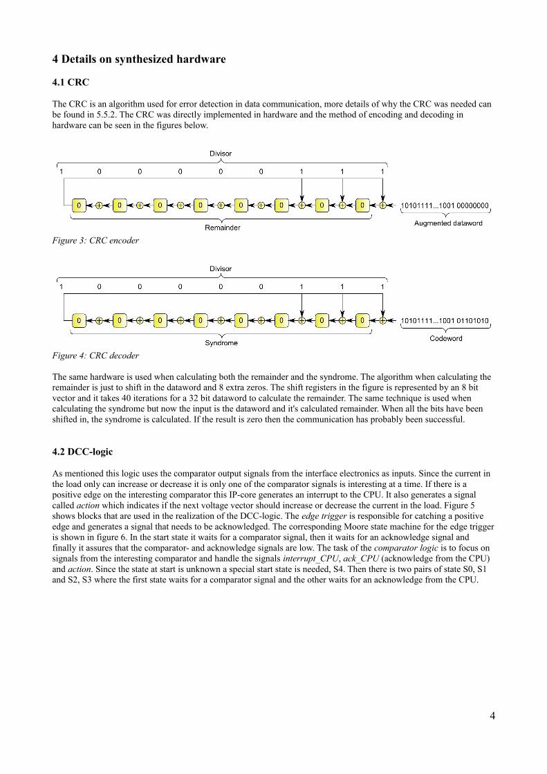
The CRC is an algorithm used for error detection in data communication, more details of why the CRC was needed can be found in 5.5.2. The CRC was directly implemented in hardware and the method of encoding and decoding in hardware can be seen in the figures below.
The same hardware is used when calculating both the remainder and the syndrome. The algorithm when calculating the remainder is just to shift in the dataword and 8 extra zeros. The shift registers in the figure is represented by an 8 bit vector and it takes 40 iterations for a 32 bit dataword to calculate the remainder. The same technique is used when calculating the syndrome but now the input is the dataword and it's calculated remainder. When all the bits have been shifted in, the syndrome is calculated. If the result is zero then the communication has probably been successful.
4.2 DCC-logic
As mentioned this logic uses the comparator output signals from the interface electronics as inputs. Since the current in the load only can increase or decrease it is only one of the comparator signals is interesting at a time. If there is a positive edge on the interesting comparator this IP-core generates an interrupt to the CPU. It also generates a signal called action which indicates if the next voltage vector should increase or decrease the current in the load. Figure 5 shows blocks that are used in the realization of the DCC-logic. The edge trigger is responsible for catching a positive edge and generates a signal that needs to be acknowledged. The corresponding Moore state machine for the edge trigger is shown in figure 6. In the start state it waits for a comparator signal, then it waits for an acknowledge signal and finally it assures that the comparator- and acknowledge signals are low. The task of the comparator logic is to focus on signals from the interesting comparator and handle the signals interrupt_CPU, ack_CPU (acknowledge from the CPU) and action. Since the state at start is unknown a special start state is needed, S4. Then there is two pairs of state S0, S1 and S2, S3 where the first state waits for a comparator signal and the other waits for an acknowledge from the CPU.
4
Figure 3: CRC encoder
Figure 4: CRC decoder

Figure 6: State diagram for Edge Trigger Figure 7: State diagram for Comparator Logic
5
Figure 5: Block diagram of DCC logic

4.3 Block diagram
The block diagram of the system is presented in figure 8. Here we find the Microblaze and bram. The CRC IP-core is above the Microblaze and connected with a FSL bus. The other custom IP-core, dcclogic, is connected to the PLB bus. On the PLB bus there are also other standard IP-cores for leds, buttons and the RS-232 communication. There are four timer modules which means that there are 8 hardware timers. Two of those are used by the serial communication and two more for the high switching frequency protection. One is used for the timeout for the vector selector and the other in that module is used as a counter to determine the period time of the switching. The two remaining timers are intended to be used by the Reference mover but that is not the case yet.
4.4 Device occupancy for hardware
Number of: System CRC DCC Logic Available
Slices Registers 3690 21,28% 66 0,38% 287 1,65% 17344
4 input LUTs 4670 26,93% 118 0,68% 245 1,41% 17344
Occupied Slices 3811 43,00% 8672
Bounded IOBs 63 25,20% 250
RAMB16s 17 60,71% 28
6
Figure 8: Block diagram

5 Details on software
5.1 The LYTMA-kernel
The software will have to do many things more or less simultaneously and to be able to achieve this an operating system was developed. It is a cooperative operating system witch means that the operating system does not preempt the tasks. Instead threads hands over the control to the operating system when they are done the ongoing moment of the task. When the operating system gets the control from a task it decides which thread that runs next. Using a cooperative operating system have some benefits, one is that thread switching is fast since the state of the processor does not need to be saved. It is also very easy to communicate between threads with a shared variable and the mutual exclusion comes automatically since a thread can not be preempted. The cons with not having preemption is that the performance of the system is dependent on all threads, and that must be taken into account in the programming of any thread.
The operating system developed in the course is called the LYTMA-kernel. It is based on the principles described above and is a small and simple way to implement a operating system. The simplicity makes it is easy to change the specifications of the LYTMA-kernel if the application demands it. The specifications of the LYTMA-kernel used in this project are:
• Up to a total of 32 threads.• High priority threads running with priority, the thread that is added first gets the highest priority.• Low priority threads running in a Round-robin fashion if no high priority threads wants to run.
5.2 Implementation of the LYTMA-kernel
The threads are implemented using functions that do not have any input arguments and return an integer that tells the kernel if the thread finished successfully. To organize the treads the kernel has a vector with function pointers to threads and to organize when to run them it uses an unsigned int called taskQ. The taskQ is used as a bit vector where each bit corresponds to a thread. If a bit in the taskQ is one it indicates that the corresponding thread wants to run. When a thread is added in the initialization of the system the kernel gives it a number. The number is used as index in the taskQ and the function pointer to the thread is stored in the vector with function pointers at that index. The enumeration of high priority threads start at index zero and it start at the maximum index in the taskQ for low priority threads. The function that starts the kernel is basically an infinite loop. The loops starts to check if there is any high priority thread that wants to run and if that is the case then it is executed using the function pointer. It repeats this until no one of the high priority threads wants to run. Then it checks if a low priority thread wants to run, if so it is executed and the loop starts over again. If there is no low priority thread that wants to run, the loop starts over again.
5.3 Develop software using the LYTMA-kernel
Using a kernel like the LYTMA-kernel automatically makes some demands on the programming of threads, interrupt routines and the initialization of the system. Threads are scheduled in interrupt routines and in other threads and are descheduled by the threads them selves. To communicate between threads global variables or as in the case of this project a global struct containing the variables that are used. To keep the code clean and simple to follow the use of shared variables in interrupt routines should be avoided, instead the interrupt routine should schedule a thread to use the shared variable. Since the kernel is used in a custom system, the programmer could break this rule if there for example are performance benefits. To initialize the kernel, every thread are added using a function provided with the kernel.
5.4 Vector
The implementation of functional blocks dealing with the voltage vector are gathered in a file named vector.c and the corresponding vector.h. There are two threads used in that file, comparatorVectorSelectorTask – which changes the voltage vector on a interrupt from the DCC-logic, and timeoutVectorSelectorTask – which changes the voltage vector on a interrupt from the timeout.
There are also three interrupt routines associated and implemented in vector.c. The timer for the high switch frequency protection must expire before the transistor can be turned on again. To update the global variable handling this safetyTimerIntH is used. The interrupt routine associated with the vector selector time out is timeoutCounterIntH and simply schedules timeoutVectorSelectorTask. The other timer in the xps_timer module is used for measuring the time
7

between switches so if it is generating an interrupt the controller has stopped switching. Finally we have the comparatorIntH witch schedules comparatorVectorSelectorTask on an interrupt from the DCC-logic.
5.5 Hysteresis band
Since the reference mover is rather isolated from the other functional blocks it has it own files, hyst.c and hyst.h. They describe one thread, changeAllowedLadderTask, which changes the allowed reference and is then scheduled again to change the other when there is a new voltage vector. The idea is to make the reference move closer to the desired mean value of the current if there it to long time before a interrupt from the DCC-logic. This has not been implemented but a timer has been instantiated and there is an interrupt routines that should handle this in hyst.c called hystTimerIntH.
5.6 Serial communication
5.6.1 Serial protocol
In the creating of the serial protocol a lot of thinking has been spent on trying to create an as safe and robust communication as possible. The computer were chosen as master and the FPGA as slave. The procedure is described in the sections below.
5.6.2 Choice of error detecting method in serial communication
Since the currents, voltages and the derivatives of these quantities can be large in power electronic environments there is a great risk for electromagnetic interference which can disturb the communication. The interference could potentially create dangerous situations if a command sent from the the computer to the FPGA is scrambled. This makes it necessary to implement some sort of error detecting method in the serial communication.
There are some different types of error detecting and correction methods and the method that were chosen was the cyclic redundancy check (CRC) due to it's performance. The CRC method can be used in error correction but the emphasis has been to find error in the communication and not to correct them even if it is possible.
The CRC method is to find the remainder of the dataword that is sent in a packet. To be able to create a remainder one has to chose a divisor and thereby indirectly decide the size of the CRC. This is because of the number of bits the divisor needs to be represented by will automatically decide the CRC size. The 9-bit divisor 26310 were chosen and this is the standard CRC-8 (the most significant bit is not needed in the calculation). The remainder of the dataword will be added after the dataword and this is called the codeword. When the codeword has been received it can checked by dividing it with the divisor and if the remainder of the division is zero then it is very likely that packet hasn't been scrambled.
The chosen divisor makes it possible to detect single-bit errors, two isolated single-bit error up to 256 bits between them, odd numbers off errors and all burst errors up to 9 bits. The probability to find burst errors with lengths of 10 bits is 99.6 % and with burst errors with length longer than 10 bits the probability is 99.8 %.
This makes the CRC-8 quite strong in finding eventual interference in the communication.
5.6.3 Packet design
Since the communication between the FPGA and the computer is using the RS-232 standard, all the data is sent in form of bytes. This means that all the different parts of the packet is divided in 8-bit parts. It is thereby understood that each part of the packet is a byte if nothing else is implied. Below is an figure of the packet design.
8
Figure 9: Packet design

In the early design of the packets an identification part seemed like a good idea so that both the computer and the FPGA could know what kind of packet it had received and the size of the packet. The packet ID were therefor decided to be the first part of the packet. It also got it's own CRC in order to be as sure as possible that the packet ID received were right. There are a couple of different packet ID types defined, the packets from the computer to the FPGA are numbered from 0 and upwards. The packets sent from the FPGA to the computer has packet ID's numbered from 255 and downwards.
The packet ID's from the computer to the FPGA are:
MODE = 0REQUEST = 1MAXCURR = 2REFCURR = 3REFSWITCHFREQ = 4TIMEOUTSWITCH = 5UPPERREF = 6LOWERREF = 7
The packet ID's from the FPGA to computer are:
CALACK = 252REQUESTEDFREQ = 253NACK = 254ACK = 255
The packet ID's makes it possible to have different size of each packet which makes the communication somewhat more complicated but it also makes it possible to minimizes the transmission time.
The second part of the packet is the data part which consist of the the dataword and it's CRC. The size of the dataword is either 1,2 or 4 bytes long, the CRC decoder and encoder are not designed for more than 4 bytes. If the dataword is longer than one byte it will have to be broken down into several bytes and when received it will be rebuilt again. The packet ID will therefor also tell the receiver what data types the dataword were before it was broken down. What each packet ID stands for must be written in both the computer and FPGA code. In other words if a new packet is added the code has to be changed in both instances.
Table 1: Description of the different packets.Type of packet ID Packet descriptionMODE This packet contains what kind of mode the user wants the FPGA to be in, it can for example
be IDLE which means that the FPGA will go into idle mode and set the voltage vectors into a zero vector.
REQUEST This packet could contain a command that the user wants something back from the FPGA like a variable or it can be that the user want's the FPGA to run some particular function
REFCURR,REFSWITCHFREQ,TIMEOUTSWITCH,UPPERREF,LOWERREF
These packets are used when sending different variable values from the computer to the FPGA.
CALACK This is an acknowledge packet which contains variable data obtained in the calibration. The calibration is discussed in section 9.
REQUESTEDFREQ This is an acknowledge packet which contains the latest switch period time from the FPGA.NACK This packet is exactly what is sounds like and it tells the computer that some of the CRC
syndrome wasn't zero. This is the only packet that's only two bytes long.ACK This packet is an acknowledge from the FPGA to the computer.
9
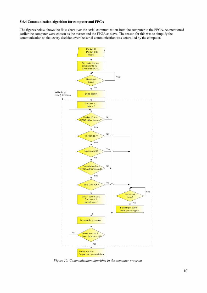
5.6.4 Communication algorithm for computer and FPGA
The figures below shows the flow chart over the serial communication from the computer to the FPGA. As mentioned earlier the computer were chosen as the master and the FPGA as slave. The reason for this was to simplify the communication so that every decision over the serial communication was controlled by the computer.
10
Figure 10: Communication algorithm in the computer program

Something that is not showed in the flow chart is the timers that is used in both the computer and the FPGA. In the computer there is a timer that automatically sends PING packets to the FPGA and if somethings goes wrong in the communication the computer will stop the possibility to send and receive packets. In the FPGA there is a timer that is reset every time a packet is received and if the timer reaches it is timer value it will put the FPGA in the STOP mode. This will happen if the serial communication has been activated and if there is something that has gone wrong in other words the computer has stopped sending packets or something is wrong with the serial cable.
To implement the algorithm showed in figure 11 following threads has been written, packetCheckerTask, packetActionTask, ackTask and nackTask. Some interrupt handlers is also involved in the serial communication. There is one to handle the 20 ms wait namely serialTimerIntH, this handler is also used for the timer that stops the FPGA if the serial communication is lost. The receiveH and sendH is the interrupt handlers for the xps_uartlite.
11
Figure 11: Communication algorithm in the FPGA program

6 External hardware
This solution of a DCC needs some special hardware, in figure 2 it is called interface electronics. Figure 12 is a more detailed view of this block. The DA-converters is one of the simplest, namely R-2R resistor ladders. The one bit flash AD-converters mentioned before is the comparators in figure 12. The function will be as follows, the references are set
to correspond to the desired current ± hysterises band2
. If the signal from the current crosses a reference the
corresponding comparator switches.
7 Simulator
Since power electronics is expensive it is important to verify that the controller is not doing anything that would harm it. To test the DCC the external feedback signals are needed, this means that some way of generating these signals based on the outputs from the controller is needed. The solution was to build a simulator for the external electronics and a motor with a mechanical load. The simulator was implemented using another FPGA board and is made as simple as possible. It uses a numerical version of the differential equations associated with a motor with a mechanical load.
12
Figure 12: Interface electronics
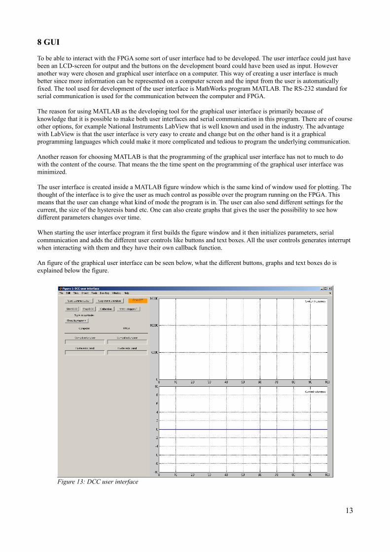
8 GUI
To be able to interact with the FPGA some sort of user interface had to be developed. The user interface could just have been an LCD-screen for output and the buttons on the development board could have been used as input. However another way were chosen and graphical user interface on a computer. This way of creating a user interface is much better since more information can be represented on a computer screen and the input from the user is automatically fixed. The tool used for development of the user interface is MathWorks program MATLAB. The RS-232 standard for serial communication is used for the communication between the computer and FPGA.
The reason for using MATLAB as the developing tool for the graphical user interface is primarily because of knowledge that it is possible to make both user interfaces and serial communication in this program. There are of course other options, for example National Instruments LabView that is well known and used in the industry. The advantage with LabView is that the user interface is very easy to create and change but on the other hand is it a graphical programming languages which could make it more complicated and tedious to program the underlying communication.
Another reason for choosing MATLAB is that the programming of the graphical user interface has not to much to do with the content of the course. That means the the time spent on the programming of the graphical user interface was minimized.
The user interface is created inside a MATLAB figure window which is the same kind of window used for plotting. The thought of the interface is to give the user as much control as possible over the program running on the FPGA. This means that the user can change what kind of mode the program is in. The user can also send different settings for the current, the size of the hysteresis band etc. One can also create graphs that gives the user the possibility to see how different parameters changes over time.
When starting the user interface program it first builds the figure window and it then initializes parameters, serial communication and adds the different user controls like buttons and text boxes. All the user controls generates interrupt when interacting with them and they have their own callback function.
An figure of the graphical user interface can be seen below, what the different buttons, graphs and text boxes do is explained below the figure.
13
Figure 13: DCC user interface
Start communication
This button will activate the serial communication and the serial timer. The orange Com OFF indicator will turn green and says Com ON. The serial timer is used to make sure that there are continuous communication between the computer and the FPGA. The reason is that the computer and the FPGA wants to know that the link between them is working. The settings for the communication is already initialized when the user interface is started.
Stop communication
This button will just deactivate the serial communication and stop the serial timer.
Start DCC
The Start DCC button will start the callback function that sends a packet with a new mode for the controller. What kind of mode it sends depends on what kind of controller the user has chosen. The modes that the user can chose is the type of controller. Right now there are only one type of controller and that is the fixed hysteresis. If the fixed hysteresis button has not been pushed the Start DCC button will just send a so called IDLE packet.
Stop DCC
When pushing the Stop DCC button the computer will send a stop packet which will set the current reference to zero which means that the motor will lose all its torque and the angular speed will decrease.
Calibration
This button will start another window that is made for calibration of the comparator logic. The window is shown in figure 16.
Motor stopped?
When the user wants to stop the motor he will push the Stop DCC button and when the motor has stopped he can confirm this by pushing the Motor stopped? button. By pushing the Motor stopped? button the user will turn the FPGA mode into IDLE and this means that the switching will stop and a zero vector will be put out on the power electronics. If the controller goes directly from controlling a running motor into IDLE mode then almost all of the motors kinetic energy will be transformed into heat in the semiconductors. This will correspond to a very large deceleration that in most cases is undesired and that is why the motor has to stand still when the user pushes the button. If the controller would have a speed signal then this button would have been unnecessary.
Fixed hysteresis
When pushing this button the mode variable in the computer program will be saved as Fixed hysteresis and the program will send the stop mode to the controller. After pushing the Motor stopped? button the Fixed hysteresis mode can be sent to the FPGA when pushing the Start DCC button.
Switch frequency graph
This graph will be updated with the controllers switching frequency. This is a interesting value for the designer of the hysteresis controller to see how it is affected by different parameter settings. The controller sends the period time of the switching if the computer requests it. Today the serial timer sends PING packets to the controller but that can be changed into GETSWITCHFREQ packets that will be used in updating the switching frequency graph.
Current reference graph
This graph is meant to be updated synchronously with the switch frequency graph so that the user can see the eventual difference in the switch frequency when using different current references. This does not mean that there is a direct correlation between the size of the current and the switching frequency since there are other factors that also changes the switching frequency but it is still interesting to see them both.
14

9 Manual
The manual is primarily intended to explain how to hook up the current controller and the simulator and how to run them.
First of all the current controller and the simulators peripheral connectors need to be connected to each other. The peripheral Pmod pin configuration for the current controller and the simulator is described in the figures below.
Now connect a serial cable from the simulator to a computer with MATLAB software and a serial cable from the current controller to a computer with MATLAB software. Download the bitstreams to the FPGA's. Open the test_av_verification.m file for the computer connected to the simulator FPGA and check that right serial port is set in the code. Run the test_av_verification.m program and the angular speed and current will be displayed in the command window. The angular speed is in unity of rad/s and the current unity is mA. The autoclose function can be used to close the serial communication. There has been thoughts of improving the test_av_verification so that the values received is plotted instead. The serial communication is also one thing that need to be improved but the there has not been time enough. This is because the idea of the simulator came to late in the project. Open the GUI_DCC.m file and check that the right serial port is set in the code (this is for the computer connected to the current controller FPGA). Run the GUI_DCC and the user interface will start. Next step is to start the communication using the Start communication button. If the communication is working as it is supposed the indicator will turn green and says Com ON. Insert a zero in the reference current box under the computer text, then insert a desired value of the hysteresis band and the computer will send a packet with all the settings the controller needs. To start the controller push the Fixed hysteresis button and then the Motor stopped? button. The controller is now ready to start and this is triggered by pushing the Start DCC button. Now the user can choose different current references and hysteresis bands freely. When stopping the motor the user can choose to push the Stop DCC button or just set the current to zero. When the motor has stopped push the Motor stopped? button and the controller stops to switching the power electronics.
15
Figure 14: Peripheral Pmod pin configuration for the DCC FPGA
Figure 15: Peripheral Pmod pin configuration for the simulator FPGA

The Calibration button on the user interface starts another window that is used in the measurement of the zero current value and the ampere per step value for the comparators. The figure below shows the calibration window.
The user must input a test current, a calibrated max current and push the Start calibration button, the FPGA will now run the calibration routine. The result will be visualized in the text boxes to the right. If the values seems to be in order then it is OK to press the Calibration OK button but if something appears to be wrong with the values the user should use the Abort calibration button. Below is a brief explanation of the different indicators.
• Progress indicator turns to green when the Start calibration button is pressed.• Fail indicator turns to red when there is some serious errors in the calibration.• Done indicator turns green when the calibration is completed• Communication error indicator turns red when there is some sort of error in the serial communication
16
Figure 16: Calibration user interface

10 Problems
• A lot of time was spent in figuring out how to set the peripheral Pmod pins.
• When testing the DCC logic we found out that it got stuck in a certain state. When simulation of the behavior of DCC logic it worked perfectly and the problem with the DCC logic has not been solved yet.
• The time between the DCC logic interrupt and the voltage vector change was measured. The delay time were found to be larger than acceptable and some optimization is needed before the current controller can be tested on real power electronics.
• For some IP cores it was not possible to use pointers in interrupt handlers when the pointer and the interrupt handler was defined in other files than in main.
11 Lesson learned
• The use of the kernel made it much easier to build the whole system since each member did not have to think to much about the other software when developing different parts of the project.
• Much of the code were well thought through before it was written which was important especially in the beginning of the project when there was no way of really testing the system. When the simulator was built it became somewhat easier to test the system.
• The group underestimated the complexity of the project that grew larger than first expected.
12 Contributions
The idea to implement a DCC with the possibility to work with variable hysteresis was originally a idea that came up in a discussion with Mats Alaküla. Since Jon have studied power electronics with great interest he thought about how to do such controller over several cups of coffee. His talent in analog electronics led to the conclusion to use comparators to tell when it is time to do something. The idea was further developed in collaboration with Per when he told Jon about the performance and possibilities of using FPGA's. In a way Jakob was involved all the time during the discussions and when it was settled that the project were going to take place he started to simulate the fundamental parts of the system. This resulted in a lot of preparatory work for everyone to figure out which parts that should be a part of the system. The main pseudo code, structure and finally program code was developed by Jon and Per while Jakob developed the serial interface and the graphical user interface. At this time the problem with the first testings with real power electronics was discovered, so Jon started sketch on the simulator while Per created the LYTMA-kernel. The rest of the work could be summarized in some residual programming and troubleshooting, and at this time the responsibilities was distributed in a way that makes it impossible to give credit to anyone else than the whole project group.
17
13 Sources
Mats Alaküla and Per Karlsson,Power Electronics: Devices, Converters, Control and Applications, Department of Industrial Electrical Engineering and Automation, 2006.
Behrouz A. Forouzan, Data Communications and Networking, Fourth Edition, 2007
Franco Maloerti, Data Converters, 2007
NEXYS2 Reference Manual, http://www.digilentinc.com/Data/Products/NEXYS2/Nexys2_rm.pdf
KISS Kernel, http://www.frontiernet.net/~rhode/kisskern.html#SchedTask
Microsoft support, November 15, 2006, http://support.microsoft.com/kb/117567
18