design of fpga based traffic light controller system
TRANSCRIPT

A Main Project Report
On
“DESIGN OF FPGA BASED TRAFFIC LIGHT
CONTROLLER SYSTEM”
Submitted in partia l fu l f i l lment of requirements
For the award of the Degree of
BACHELOR OF TECHNOLOGY
IN
ELECTRONICS & COMMUNICATION ENGINEERING
By
B.VINEETHA (11RQ1A0486)
Under the Guidance of
Mr. MD.MUSTAQ AHMED
[M.Tech]
Asst. Professor
DEPARTMENT OF ELECTRONICS & COMMUNICATION ENGINEERING
MINA INSTITUTE OF ENGINEERING & TECHNOLOGY FOR WOMEN
(Approved by AICTE, New Delhi, Affiliated to JNTUH, Hyderabad)
Ramachandragudem, Miryalguda, Nalgonda (Dist), T.G.
2015
DEPARTMENT OF ELECTRONICS & COMMUNICATION ENGINEERING
MINA INSTITUTE OF ENGINEERING & TECHNOLOGY FOR WOMEN
(Approved by AICTE, New Delhi, Affiliated to JNTUH, Hyderabad)
Ramachandragudem, Miryalguda, Nalgonda (Dist), T.G. 2015
CERTIFICATE
This is to certify that the dissertation entitled “DESIGN OF FPGA BASED
TRAFFIC LIGHT CONTROLLER SYSTEM” that is being submitted by
B.VINEETHA (11RQ1A0486) in partial fulfillment for the award of the Degree of
BACHELOR OF TECHNOLOGY IN ELECTRONICS &
COMMUNICATION ENGINEERING from Jawaharlal Nehru Technological
University, Hyderabad. This is a bonafide work done by her under my guidance and
supervision from January 2015 to March 2015.
Internal Guide Head of the Department
Mr. MD.MUSTAQ AHMED Mr. MD.MUSTAQ AHMED
[M.Tech] [M.Tech]
Asst. Professor Asst. Professor
External Examiner Principal
Mr. PANDU RANGA REDDY

ACKNOWLEDGEMENT
The satisfaction that accompanies the successful completion of any task would
be incomplete without the mention of the people who made it possible and whose
constant guidance and encouragement crown all the efforts success.
I am extremely grateful to our respected Principal, Mr. PANDU RANGA
REDDY for fostering an excellent academic climate in our institution. I also express
my sincere gratitude to our respected Head of the Department Prof. Mr. MD.
MUSTAQ AHMED for his encouragement, overall guidance in viewing this project
a good asset and effort in bringing out this project.
I would like to convey thanks to our Project guide at college Prof. Mr. MD.
MUSTAQ AHMED for his guidance, encouragement, co-operation and kindness
during the entire duration of the course and academics.
I am deeply indebted to our Project trainer Mr. ANIL GAUD of Kit Tech
Solutions for regular guidance and constant encouragement and I am extremely
grateful to him for his valuable suggestions and unflinching co-operation throughout
project work.
Last but not the least we also thank our friends and family members for
helping us in completing the project.
B.VINEETHA (11RQ1A0486)

DECLARATION
I do here by declare that the main project work titled by “DESIGN OF FPGA
BASED TRAFFIC LIGHT CONTROLLER SYSTEM” submitted by me to the
JNTU in partial fulfillment of the requirement for the award of bachelor of technology
in Electronics & Communication Engineering is my original work. The concept,
analysis, design, layout and implementation of this project have been done by me and
my batch mates and it has not been copied or submitted from anywhere else for the
award of the degree.
Date:
Place: Miryalguda
B.VINEETHA (11RQ1A0486)

ABSTRACT
In this project we proposed a design of a modern FPGA-based Traffic Light
Control (TLC) System to manage the road traffic. The approach is by controlling the
access to areas shared among multiple intersections and allocating effective time
between various users, during peak and off-peak hours.
The implementation is based on real location in a city in Telangana where the
existing traffic light controller is a basic fixed-time method. This method is inefficient
and almost always leads to traffic congestion during peak hours while drivers are
given unnecessary waiting time during off-peak hours. The traffic light controller
consists of traffic signals (Red, Yellow/Amber & Green).
Then we have taken the real time waveform as well as the simulated
waveform for different frequencies. The proposed design is a more universal and
intelligent approach to the situation and has been implemented using FPGA. The
system is implemented on ALTERA FLEX10K chip and simulation results are proven
to be successful.
Theoretically the waiting time for drivers during off-peak hours has been
reduced further, therefore making the system better than the one being used at the
moment. Future improvements include addition of other functions to the proposed
design to suit various traffic conditions at different locations.
TABLE OF CONTENTS
LIST OF FIGURES i
1. INTRODUCTION TO TRAFFIC LIGHT 1
CONTROLLER SYSTEM
1.1 AN OVERVIEW 1
1.2 RESEARCH OBJECTIVE 3
2. LITERATURE REVIEW 5
2.1 INTRODUCTION 5
2.2 PROTOCOL 6
2.3 THE OBJECTIVES 7
3. TECHNOLOGIES USED 8
4. FPGA 9
4.1 OVERVIEW 9
4.2 INTRODUCTION TO FPGA’S 10
4.3 TYPES OF FPGA’S 11
4.4 INTERNAL STRUCTURE 12
4.5 PROGRAMMING TECHNOLOGIES 13
4.5.1 SRAM BASED PROGRAMMING TECHNOLOGY 13
4.5.2 FLASH PROGRAMMING TECHNOLOGY 14
4.5.3 ANTIFUSE PROGRAMMING TECHNOLOGY 15
4.6 CONFIGURABLE LOGIC BLOCK 15
4.7 ARCHITECTURE 17
4.8 APPLICATIONS OF FPGA’S 21
5. VLSI 22
5.1 OVERVIEW OF VLSI 22
5.2 INTRODUCTION TO VLSI 23
5.3 HISTORY OF SCALE INTEGRATION 23
5.4 ADVANTAGES OF IC’S OVER DISCRETE 24
COMPONENTS
5.5 VLSI AND SYSTEMS 25
5.6 ASIC 25

5.7 APPLICATIONS 27
6. VERILOG HDL 28
6.1 OVERVIEW 28
6.2 HISTORY 30
6.2.1 BEGINNING 30
6.2.2 VERILOG 1995 30
6.2.3 VERILOG 2001 30
6.2.4 VERILOG 2005 31
6.2.5 SYSTEM VERILOG 31
6.3 DESIGN STYLES 33
6.3.1 BOTTOM-UP DESIGN 33
6.3.2 TOP-DOWN DESIGN 33
6.4 ABSTRACTION LEVELS OF VERILOG 33
6.4.1 BEHAVIORAL LEVEL 34
6.4.2 REGISTER TRANFER LEVEL 34
6.4.3 GATE LEVEL 34
6.5 ADVANTAGES 35
7. XILINX 36
7.1 MIGRATING PROJECTS FROM PREVIOUS ISE 36
SOFTWARE RELEASES
7.2 PROPERTIES 36
7.3 IP MODULES 37
7.4 OBSOLETE SOURCE FILE TYPES 37
7.5 USING ISE EXAMPLE PROJECTS 37
7.5.1 TO OPEN AN EXAMPLE 37
7.5.2 CREATING A PROJECT 38
7.5.3 CREATING A COPY OF A PROJECT 39
7.5.4 CREATING A PROJECT ARCHIVE 41
8. BLOCK DIAGRAM 43
9. THE STATE MACHINE 44
9.1 THE FINITE STATE MACHINE 44
9.1.1 DEFINITION OF THE FSM 44
9.1.2 NOTION OF STATES IN SEQUENTIAL 45

9.1.2.1 WORKING PRINCIPLE OF AN ASM 45
9.1.3 IMPLEMENTATION OF A FSM 46
9.1.4 ADVANTAGES OF FSM 47
9.2 TYPES OF STATE MACHINES 47
9.2.1 MEALY MACHINE 47
9.2 2 MOORE MACHINE 48
9.2.3 MECHANISM 49
9.2.4 FSM DESIGN TECHNIQUES 49
9.2.5 CLASSICAL DESIGN APPROACH 50
9.2.6 VHDL FSM DESIGN APPROACH 50
10. TRAFFIC LIGHT CONTROLLER 52
IMPLEMENTATION USING FPGA
10.1 ROAD STRUCTURE 52
10.2 TIMING SETTING 53
10.3 VHDL MODEL 54
11. SOURCE CODE 55
12. RESULT 64
12.1 RTL SCHEMATICS 64
12.2 SIMULATION RESULTS 67
13. FEATURES 69
13.1 ADVANTAGES 69
13.2 APPLICATIONS 69
13.3 PAST TECHNOLOGIES AND THEIR DRAWBACKS 69
13.3.1 USING MICROCONTROLLER 69
13.3.2 USING PLD AND CPLD 69
13.4 FUTURE ENHANCEMENT 69
14. CONCLUSION 71
15. REFERENCES 72

LIST OF FIGURES
SNO FIGURE PAGE NO
1. CROSSOVER BETWEEN SIDE ROAD AND HIGHWAY 1
2. TYPES OF FPGA’S 11
3. SILICON WAFER CONTAINING 10,000 GATE FPGA’S 12
4. SINGLE FPGA DIE 12
5. A TYPICAL FPGA STRUCTURE 12
6. OVERVIEW OF FPGA ARCHITECTURE 13
7. STATIC MEMORY CELL 14
8. BASIC LOGIC ELEMENT 16
9. OVERVIEW OF MESH BASED FPGA ARCHITECTURE 17
10. EXAMPLE OF SWITCH AND CONNECTION BOX 18
11. SWITCH BOX 19
12. CHANNEL SEGMENT DISTRIBUTION 20
13. ALTERA’S STRATIX BLOCK DIAGRAM 20
14. BLOCK DIAGRAM OF TRAFFIC LIGHT CONTROLLER 43
SYSTEM
15. A POSSIBLE FINITE STATE MACHINE 46
16. MEALY MACHINE 48
17. MOORE MACHINE 49
18. STATE DIAGRAM FOR TRAFFIC LIGHT CONTROLLER 51
19. ROAD STRUCTURE 52
20. THE CONTROL SCHEME DURING PEAK HOUR 53
21. RTL SCHEMATIC 64
22. RTL SCHEMATIC WITH 4 COUNTERS, ADDER, 65
D FLIPFLOP, 4 COMPARATORS, INVERTOR, FSM
23. RTL SCHEMATIC ZOOM IN 67
24. SENSOR1-0, SENSOR2-0 67
25. SENSOR1-0, SENSOR2-1 68
26. SENSOR1-1, SENSOR2-0 68
27. SENSOR-1, SENSOR2-1 68

1. INTRODUCTION TO TRAFFIC LIGHT
CONTROLLER SYSTEM
1.1 AN OVERVIEW
Traffic lights are integral part of modern life. Their proper operation can spell
the difference between smooth flowing traffic and four-lane gridlock. Proper
operation entails precise timing, cycling through the states correctly, and responding
to outside inputs. The traffic light controller is designed to meet a complex
specification. That specification documents the requirements that a successful traffic
light controller must meet. It consists of an operation specification that describes the
different functions the controller must perform, a user interface description specifying
what kind of interface the system must present to users, and a detailed protocol for
running the traffic lights. Each of these requirements sets imposed new constraints on
the design and introduced new problems to solve. The controller to be designed
controls the traffic lights of a busy highway (HWY) intersecting a side road (SRD)
that has relatively lighter traffic load. Figure 1.1 shows location of the traffic lights.
Sensors at the intersection detect the presence of cars on highway and side road.
Fig 1.1 Crossover between side road and highway

The heart of the system is a Finite State Machine (FSM) that directs the unit to
light the main and side street lights at appropriate times for the specified time
intervals. This unit depends on several inputs which are generated outside the system.
In order to safely process these external inputs, we can design an input handler that
synchronizes asynchronous inputs to the system clock. The input handler also latches
some input signals and guarantees that other input signals will be single pulses,
regardless of their duration. This pulsification greatly simplifies the design by
ensuring that most external inputs are high for one and only one clock cycle. In
addition to the FSM and input handler, the design also includes a slow clock
generator. Because the specification requires that timing parameters are specified in
seconds, the controller needs to be informed every second that a second of real time
has elapsed. The slow clock solves this problem by generating a slow clock pulse that
is high for one cycle on the system clock during every second of real time. In addition
to generating a once per second pulse, we need to be able to count down from a
specified number of seconds. The timer subsystem does that job. When given a
particular number of seconds to count down from, it informs the FSM controller after
exactly that number of seconds has elapsed. Finally, we have storage and output
components. In order to store the users timing parameters, we use a static RAM
whose address and control lines are supplied by the FSM. The RAM data lines are on
a tri-state bus which is shared by the timer unit and a tri-state enabled version of the
data value signals. This same bus can drive the HEX-LED display, which comprises
the output subsystem along with the actual traffic light LEDs. The heart of the
controller is the FSM. This FSM controls the loading of static RAM locations with
timing parameters, displaying these parameters by reading the RAM locations, and
the control of the actual traffic lights. The timer and the divider control various timing
issues in the system. The timer is a counter unit that counts for a number of one
second intervals that are specified by data stored in the static RAM. The divider
provides a one-second clock that is used by the timer as a count interval. Lastly, the
synchronizers ensure that all inputs to the FSM are synchronized to the system clock.

1.2 RESEARCH OBJECTIVE
The objective of our work is to implement a Traffic light Control system for a
four road junction with FPGA.As the FPGA is a new technology to the country. These
advanced technology implementations will lead the countries systems in the near
future. So for a better future, it’s today we have to work with.
Field Programmable Gate Array (FPGA) is an Integrated Circuit (IC) that
contains an array of identical logic cells that can be programmed by the user. The
ALTERA FLEX10K provides high density logic together with RAM memory in each
device. FPGA has many advantages over microcontroller in terms of speed, number
of input and output ports and performance. FPGA is also a cheaper solution compared
to ASICs (custom IC) design which is only cost effective for mass production but
always too costly and time consuming for fabrication in a small quantity.
Traffic light controller (TLC) is used to lessen or eliminate conflicts at area
shared among multiple traffic streams called intersections, by controlling the access to
the intersections and apportioning effective period of time between various users. The
main goal of this project is to manage the traffic movement of four intersecting roads
and to achieve optimum use of the traffic. In general, traffic lights of all main roads
are controlled with a fix-time control system while smaller roads are controlled
autonomously by sensors.
During rush hours, when people are going to work or going back home, traffic
is at the maximum capacity and without an effective TLC system, will almost always
resulting in traffic jams. This problem arises due to the unbalance traffic flow from
only certain directions on huge intersections, which is causing a major congestion on
the affected directions and at the same time having an un-optimized use of traffic on
the less congested direction. Approach has been made by putting the traffic policemen
in charge of the traffic instead of the traffic lights during the peak hours thus showing
the ineffectiveness of the system in the most demanding situation. This project aims to
address this major flaw and hopefully come out with a better solution to the problem.
Many research works have been done on traffic light controller using different
controlling methods. Chavan, Deshpande and Rana have developed TLC based on
microprocessor and microcontroller. But, there is some limitation in this design due to
no flexibility of modification on the TLC during real time. Liu and Chen have
designed TLC using Programmable Logic Controller (PLC) to replace the relay

wiring, as a result making the design better. Kulkarni and Waingankar have proposed
a TLC design using fuzzy logic, which has the capability of mimicking the human
intelligence. This design has been implemented using MATLAB and showed that it
can control the traffic flow more efficiently compared to the fixed time control.
El-Medany and Hussain have implemented FPGA-Based 24-hour TLC that
manage traffic movement of four roads and reached maximum utilization of the traffic
during rush hour and normal time. Shi, Hongli and Yandong have designed an
intelligent TLC that can be applied both in common intersections and multiple
branches intersections based on VHDL.
The use of VHDL is preferred especially for FPGA design because VHDL can
be used to describe and simulate the operation of digital circuits ranging from few
gates to come complex one. In this project, the TLC will be design based on VHDL
using QUARTUS II and implemented in hardware by using ALTERA FLEX10K
chip.

2. LITERATURE REVIEW
2.1 INTRODUCTION
Intelligent Transportation Systems (ITS) applications for traffic signals –
including communications systems, adaptive control systems, traffic responsive, real-
time data collection and analysis, and maintenance management systems – enable
signal control systems to operate with greater efficiency. Sharing traffic signal and
operations data with other systems will improve overall transportation system
performance in freeway management, incident and special event management, and
maintenance/failure response times. Some examples of the benefits of using ITS
applications for traffic signal control include: Updated traffic signal control
equipment used in conjunction with signal timing optimization can reduce congestion.
The Texas Traffic Light Synchronization program reduced delays by 23 percent by
updating traffic signal control equipment and optimizing signal timing. Coordinated
signal systems improve operational efficiency. Adaptive signal systems improve the
responsiveness of signal timing in rapidly changing traffic conditions. Various
adaptive signal systems have demonstrated network performance enhancement from 5
percent to over 30 percent. Traffic light controller communication and sensor
networks are the enabling technologies that allow adaptive signal control to be
deployed. Incorporating Traffic light controller into the planning, design, and
operation of traffic signal control systems will provide motorists with recognizable
improvements in travel time, lower vehicle operating costs, and reduced vehicle
emissions. There are more than 330,000 traffic signals in the United States, and,
according to U.S. Department of Transportation estimates, as many as 75 percent
could be made to operate more efficiently by adjusting their timing plans,
coordinating adjacent signals, or updating equipment. In fact, optimizing signal
timing is considered a low-cost approach to reducing congestion, costing from $2,500
to $3,100 per signal per update. ITS technology enables the process of traffic signal
timing to be performed more efficiently by enhancing data collection and system
monitoring capabilities and, in some applications, automating the process entirely.
ITS tools such as automated traffic data collection, centrally controlled or monitored
traffic signal systems, closed loop signal systems, interconnected traffic signals, and
traffic adaptive signal control help make the traffic signal timing process efficient and
cost effective. Several municipalities have worked to synchronize, optimize, or

otherwise upgrade their traffic signal systems in recent years. Below is an example of
the benefits some have realized:
The Traffic Light Synchronization program in Texas shows a benefit-cost
ratio of 62:1, with reductions of 24.6 percent in delay, 9.1 percent in fuel
consumption, and 14.2 percent in stops. The Fuel Efficient Traffic Signal
Management program in California showed a benefit-cost ratio of 17:1, with
reductions of 14 percent in delay, 8 percent in fuel consumption, 13 percent in stops,
and 8 percent in travel time. Improvements to an 11-intersection arterial in St.
Augustine, Florida, showed reductions of 36 percent in arterial delay, 49 percent in
arterial stops, and 10 percent in travel time, resulting in an annual fuel savings of
26,000 gallons and a cost savings of $1.1 million. Although communications
networks allow almost instantaneous notification of equipment failure, without which
some failures may go unnoticed for months, there must be staff available to respond.
2.2 PROTOCOL
The protocol or the design rules we incorporated in designing a traffic light
controller are laid down:
We too have the same three standard signals of a traffic light controller that is
RED, GREEN, and YELLOW which carry their usual meanings that of stop
go and wait respectively.
We have two roads – the highway road and the side road or country road with
the highway road having the higher priority of the two that is it is given more
time for motion which implies that the green signal remains for a longer time
along the highway side rather than on the country side. We have decided on
having a green signal or motion signal on the highway side for a period of 80
seconds and that on the country road of 40 seconds and the yellow signal for a
time length of 20 seconds.
We can have provisions for two exceptions along the roads one along the
highway and the other along the country side which interrupt the general cycle

whenever an exceptions like an emergency vehicle or any such kind of
exceptions which have to be addressed quickly. When these interrupts occur
the normal sequence is disturbed and the cycle goes into different states
depending on its present state and the interrupt occurs.
We have taken into consideration a two way traffic that is the opposite
directions along the highway side will be having the same signals that is the
movements along the both direction on a single road will be same at any
instant of time. This ensures no jamming of traffic and any accidents at the
turnings.
2.3 THE OBJECTIVES
The following line up as the main objectives of the project.
1. Transform the word description of the protocol into a Finite State Machine
transition diagram.
2. Implement a simple finite state machine using VHDL.
3. Simulate the operation of the finite state machine.
4. Implement the design onto a FPGA.

3. TECHNOLOGIES USED
In this project, we are designing an Intelligent Transport System (ITS)
application for Traffic Light Controller (TLC) by using Field Programmable Gate
Array (FPGA). FPGA have been used for a wide range of applications. After the
introduction of the FPGA, the field of programmable logic has expanded
exponentially. Due to its ease of design and maintenance, implementation of custom
made chips has shifted.
The integration of FPGA and all the small devices will be integrated by using
Very Large Scale Integration (VLSI).
The code is written in Verilog HDL design pattern and synthesis is done in
XILINX of version 14.5.
Thus, the major technologies used in this project are:
FPGA
VLSI
Verilog HDL
XILINX 14.5 version
We will discuss about all these technologies briefly in the following chapters.

4. FPGA
4.1 OVERVIEW
A field-programmable gate array (FPGA) is a semiconductor device that can
be configured by the customer or designer after manufacturing—hence the name
"field-programmable". FPGAs are programmed using a logic circuit diagram or a
source code in a hardware description language (HDL) to specify how the chip will
work. They can be used to implement any logical function that an application-specific
integrated circuit (ASIC) could perform, but the ability to update the functionality
after shipping offers advantages for many applications.
Field Programmable Gate Arrays (FPGAs) were first introduced almost two
and a half decades ago. Since then they have seen a rapid growth and have become a
popular implementation media for digital circuits. The advancement in process
technology has greatly enhanced the logic capacity of FPGAs and has in turn made
them a viable implementation alternative for larger and complex designs. Further,
programmable nature of their logic and routing resources has a dramatic effect on the
quality of final device’s area, speed, and power consumption.
This chapter covers different aspects related to FPGAs. First of all an
overview of the basic FPGA architecture is presented. An FPGA comprises of an
array of programmable logic blocks that are connected to each other through
programmable interconnect network. Programmability in FPGAs is achieved through
an underlying programming technology. This chapter first briefly discusses different
programming technologies. Details of basic FPGA logic blocks and different routing
architectures are then described. After that, an overview of the different steps
involved in FPGA design flow is given. Design flow of FPGA starts with the
hardware description of the circuit which is later synthesized, technology mapped and
packed using different tools. After that, the circuit is placed and routed on the
architecture to complete the design flow.
The programmable logic and routing interconnect of FPGAs makes them
flexible and general purpose but at the same time it makes them larger, slower and
more power consuming than standard cell ASICs. However, the advancement in
process technology has enabled and necessitated a number of developments in the
basic FPGA architecture. These developments are aimed at further improvement in
the overall efficiency of FPGAs so that the gap between FPGAs and ASICs might be

reduced. These developments and some future trends are presented in the last section
of this chapter.
4.2 INTRODUCTION TO FPGA’S
Field programmable Gate Arrays (FPGAs) are pre-fabricated silicon devices
that can be electrically programmed in the field to become almost any kind of digital
circuit or system. For low to medium volume productions, FPGAs provide cheaper
solution and faster time to market as compared to Application Specific Integrated
Circuits (ASIC) which normally require a lot of resources in terms of time and money
to obtain first device. FPGAs on the other hand take less than a minute to configure
and they cost anywhere around a few hundred dollars to a few thousand dollars. Also
for varying requirements, a portion of FPGA can be partially reconfigured while the
rest of an FPGA is still running. Any future updates in the final product can be easily
upgraded by simply downloading a new application bitstream. However, the main
advantage of FPGAs i.e. flexibility is also the major cause of its draw back. Flexible
nature of FPGAs makes them significantly larger, slower, and more power consuming
than their ASIC counterparts. These disadvantages arise largely because of the
programmable routing interconnect of FPGAs which comprises of almost 90% of
total area of FPGAs. But despite these disadvantages, FPGAs present a compelling
alternative for digital system implementation due to their less time to market and low
volume cost.
Normally FPGAs comprise of:
Programmable logic blocks which implement logic functions.
Programmable routing that connects these logic functions.
I/O blocks that are connected to logic blocks through routing interconnect and
that make off-chip connections.
A generalized example of an FPGA is shown in Fig. 4.1 where configurable logic
blocks (CLBs) are arranged in a two dimensional grid and are interconnected by
programmable routing resources. I/O blocks are arranged at the periphery of the grid
and they are also connected to the programmable routing interconnect. The
“programmable/reconfigurable” term in FPGAs indicates their ability to implement a

new function on the chip after its fabrication is complete. The reconfigurabil-
ity/programmability of an FPGA is based on an underlying programming technology,
which can cause a change in behavior of a pre-fabricated chip after its fabrication.
4.3 TYPES OF FPGA’S
There are two basic types of FPGAs: SRAM-based reprogrammable (Multi-
time Programmed MTP) and (One Time Programmed) OTP. These two types of
FPGAs differ in the implementation of the logic cell and the mechanism used to make
connections in the device.
The dominant type of FPGA is SRAM-based and can be reprogrammed as
often as you choose. In fact, an SRAM FPGA is reprogrammed every time it’s
powered up, because the FPGA is really a fancy memory chip. That’s why you need a
serial PROM or system memory with every SRAM FPGA.
Fig 4.1: Types of FPGA’S
In the SRAM logic cell, instead of conventional gates, an LUT determines the
output based on the values of the inputs. (In the “SRAM logic cell” diagram above,
six different combinations of the four inputs determine the values of the output.)
SRAM bits are also used to make connections. OTP FPGAs use anti-fuses (contrary
to fuses, connections are made, not “blown”, during programming) to make
permanent connections in the chip. Thus, OTP FPGAs do not require SPROM or
other means to download the program to the FPGA. However, every time you make a
design change, you must throw away the chip! The OTP logic cell is very similar to
PLDs, with dedicated gates and flip-flops.
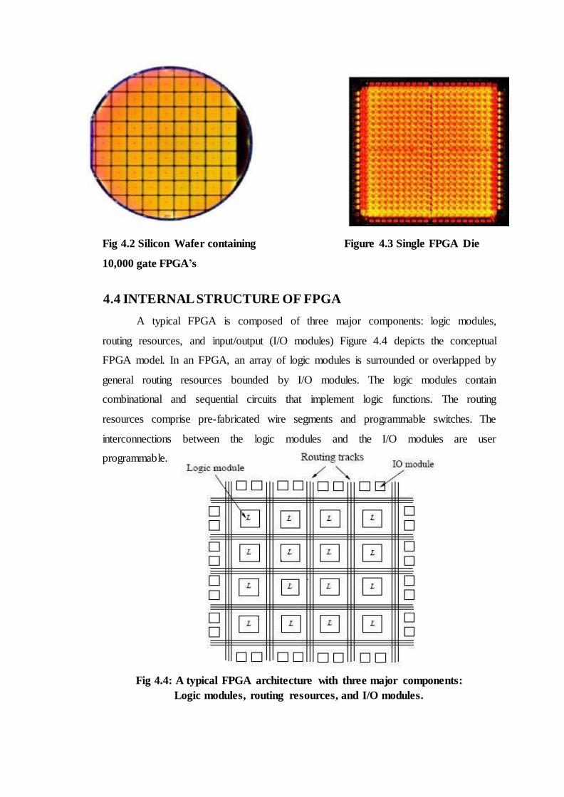
Fig 4.2 Silicon Wafer containing Figure 4.3 Single FPGA Die
10,000 gate FPGA’s
4.4 INTERNAL STRUCTURE OF FPGA
A typical FPGA is composed of three major components: logic modules,
routing resources, and input/output (I/O modules) Figure 4.4 depicts the conceptual
FPGA model. In an FPGA, an array of logic modules is surrounded or overlapped by
general routing resources bounded by I/O modules. The logic modules contain
combinational and sequential circuits that implement logic functions. The routing
resources comprise pre-fabricated wire segments and programmable switches. The
interconnections between the logic modules and the I/O modules are user
programmable.
Fig 4.4: A typical FPGA architecture with three major components:
Logic modules, routing resources, and I/O modules.

4.5 PROGRAMMING TECHNOLOGIES
There are a number of programming technologies that have been used for
reconfigurable architectures. Each of these technologies has different characteristics
which in turn have significant effect on the programmable architecture. Some of the
well known technologies include static memory, flash, and anti-fuse.
Fig. 4.5: Overview of FPGA architecture
4.5.1 SRAM-BASED PROGRAMMING TECHNOLOGY
Static memory cells are the basic cells used for SRAM-based FPGAs. Most
commercial vendors [76, 126] use static memory (SRAM) based programming
technology in their devices. These devices use static memory cells which are divided
throughout the FPGA to provide configurability. An example of such memory cell is
shown in Fig.4.7.In an SRAM-based FPGA, SRAM cells are mainly used for
following purposes:
1. To program the routing interconnect of FPGAs which are generally steered by
small multiplexors.
2. To program Configurable Logic Blocks (CLBs) those are used to implement logic
functions.

SRAM-based programming technology has become the dominant approach for
FPGAs because of its re-programmability and the use of standard CMOS process
technology and therefore leading to increased integration, higher speed and lower
dynamic power consumption of new process with smaller geometry.
Fig. 4.6: Static memory cell
There are how-ever a number of drawbacks associated with SRAM-based
programming technology. For example an SRAM cell requires 6 transistors which
make the use of this technology costly in terms of area compared to other
programming technologies. Further SRAM cells are volatile in nature and external
devices are required to permanently store the configuration data. These external
devices add to the cost and area overhead of SRAM-based FPGAs.
4.5.2 FLASH PROGRAMMING TECHNOLOGY
One alternative to the SRAM-based programming technology is the use of
flash or EEPROM based programming technology. Flash-based programming
technology offers several advantages. For example, this programming technology is
non-volatile in nature. Flash-based programming technology is also more area
efficient than SRAM-based programming technology. Flash-based programming

technology has its own disadvantages also. Unlike SRAM-based programming
technology, flash-based devices cannot be reconfigured/reprogrammed an infinite
number of times. Also, flash-based technology uses non-standard CMOS process.
4.5.3 ANTIFUSE PROGRAMMING TECHNOLOGY
An alternative to SRAM and flash-based technologies is anti-fuse
programming technology. The primary advantage of anti-fuse programming
technology is its low area. Also this technology has lower on resistance and parasitic
capacitance than other two programming technologies. Further, this technology is
non-volatile in nature. There is however significant disadvantages associated with this
programming technology. For example, this technology does not make use of
standard CMOS process. Also, anti-fuse programming technology based devices
cannot be reprogrammed.
In this section, an overview of three commonly used programming
technologies is given where all of them have their advantages and disadvantages.
Ideally, one would like to have a programming technology which is reprogrammable,
non-volatile, and that uses a standard CMOS process. Apparently, none of the above
presented technologies satisfy these conditions. However, SRAM-based programming
technology is the most widely used programming technology. The main reason is its
use of standard CMOS process and for this very reason, it is expected that this
technology will continue to dominate the other two programming technologies.
4.6 CONFIGURABLE LOGIC BLOCK
A configurable logic block (CLB) is a basic component of an FPGA that
provides the basic logic and storage functionality for a target application design. In
order to provide the basic logic and storage capability, the basic component can be
either a transistor or an entire processor. However, these are the two extremes where
at one end the basic component is very fine-grained (in case of transistors) and
requires large amount of programmable interconnect which eventually results in an
FPGA that suffers from area-inefficiency, low performance and high power
consumption. On the other end (in case of processor), the basic logic block is very
coarse-grained and cannot be used to implement small functions as it will lead to
wastage of resources. In between these two extremes, there exists a spectrum of basic
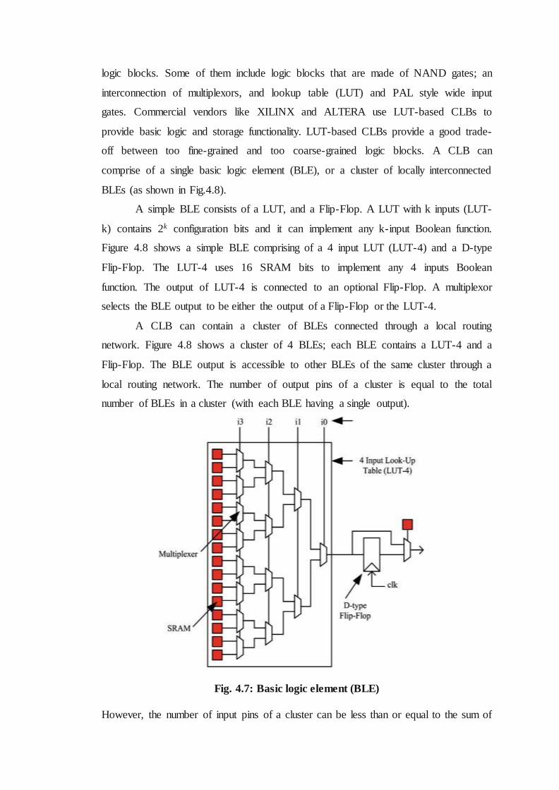
logic blocks. Some of them include logic blocks that are made of NAND gates; an
interconnection of multiplexors, and lookup table (LUT) and PAL style wide input
gates. Commercial vendors like XILINX and ALTERA use LUT-based CLBs to
provide basic logic and storage functionality. LUT-based CLBs provide a good trade-
off between too fine-grained and too coarse-grained logic blocks. A CLB can
comprise of a single basic logic element (BLE), or a cluster of locally interconnected
BLEs (as shown in Fig.4.8).
A simple BLE consists of a LUT, and a Flip-Flop. A LUT with k inputs (LUT-
k) contains 2k configuration bits and it can implement any k-input Boolean function.
Figure 4.8 shows a simple BLE comprising of a 4 input LUT (LUT-4) and a D-type
Flip-Flop. The LUT-4 uses 16 SRAM bits to implement any 4 inputs Boolean
function. The output of LUT-4 is connected to an optional Flip-Flop. A multiplexor
selects the BLE output to be either the output of a Flip-Flop or the LUT-4.
A CLB can contain a cluster of BLEs connected through a local routing
network. Figure 4.8 shows a cluster of 4 BLEs; each BLE contains a LUT-4 and a
Flip-Flop. The BLE output is accessible to other BLEs of the same cluster through a
local routing network. The number of output pins of a cluster is equal to the total
number of BLEs in a cluster (with each BLE having a single output).
Fig. 4.7: Basic logic element (BLE)
However, the number of input pins of a cluster can be less than or equal to the sum of

input pins required by all the BLEs in the cluster. Modern FPGAs contain typically 4
to 10 BLEs in a single cluster. Although here we have discussed only basic logic
blocks, many modern FPGAs contain a heterogeneous mixture of blocks, some of
which can only be used for specific purposes. Theses specific purpose blocks, also
referred here as hard blocks, include memory, multipliers, adders and DSP blocks etc.
Hard blocks are very efficient at implementing specific functions as they are designed
optimally to perform these functions, yet they end up wasting huge amount of logic
and routing resources if unused. A detailed discussion on the use of heterogeneous
mixture of blocks for implementing digital circuits is presented in Chap. 4 where both
advantages and disadvantages of heterogeneous FPGA architectures and a remedy to
counter the resource loss problem are discussed in detail.
4.7 ARCHITECTURE OF FPGA
As discussed earlier, in an FPGA, the computing functionality is provided by
its programmable logic blocks and these blocks connect to each other through
programmable routing network. This programmable routing network provides routing
connections among logic blocks and I/O blocks to implement any user-defined circuit.
The routing interconnect of an FPGA consists of wires and programmable switches
that form the required connection. These programmable switches are configured using
the programmable technology.
Fig. 4.8 Overview of mesh-based FPGA architecture

The routing network of an FPGA occupies 80–90% of total area, whereas the
logic area occupies only 10–20% area. The flexibility of an FPGA is mainly
dependent on its programmable routing network. A mesh-based FPGA routing
network consists of horizontal and vertical routing tracks which are interconnected
through switch boxes (SB). Logic blocks are connected to the routing network
through connection boxes (CB). The flexibility of a connection box (Fc) is the number
of routing tracks of adjacent channel which are connected to the pin of a block. The
connectivity of input pins of logic blocks with the adjacent routing channel is called
as Fc(in); the connectivity of output pins of the logic blocks with the adjacent routing
channel is called as Fc(out). An Fc(in) equal to 1.0 means that all the tracks of
adjacent routing channel are connected to the input pin of the logic block. The
flexibility of switch box (Fs) is the total number of tracks with which every track
entering in the switch.
Fig. 4.9: Example of switch and connection box
The routing tracks connected through a switch box can be bidirectional or uni-
directional (also called as directional) tracks. Figure 4.10 shows a bidirectional and a
unidirectional switch box having Fs equal to 3. The input tracks (or wires) in both
these switch boxes connect to 3 other tracks of the same switch box. The only
limitation of unidirectional switch box is that their routing channel width must be in
multiples of 2.
Generally, the output pins of a block can connect to any routing track through
pass transistors. Each pass transistor forms a tri-state output that can be independently
turned on or off. However, single-driver wiring technique can also be used to connect
output pins of a block to the adjacent routing tracks. For single-driver wiring, tristate

elements cannot be used; the output of block needs to be connected to the neighboring
routing network through multiplexors in the switch box. Modern commercial FPGA
architectures have moved towards using single-driver, directional routing tracks.
Authors in show that if single-driver directional wiring is used instead of bidirectional
wiring, 25% improvement in area, 9% in delay and 32% in area-delay can be
achieved. All these advantages are achieved without making any major changes in the
FPGA CAD flow.
Fig. 4.10: Switch block-length 1 wires

Fig. 4.11 Channel segment distribution
Until now, we have presented a general overview about island-style routing
architecture. Now we present a commercial example of this kind of architectures.
ALTERA’s Stratix II architecture is an industrial example of an island-style FPGA
(Figure 4.12). The logic structure consists of LABs (Logic Array Blocks), memory
blocks, and digital signal processing (DSP) blocks. LABs are used to implement
general-purpose logic, and are symmetrically distributed in rows and columns
throughout the device fabric.
Fig. 4.12 ALTERA’s stratix-II block diagram

4.8 APPLICATIONS OF FPGA’S
FPGA’s have gained rapid acceptance and growth over the past decade
because they can be applied to a very wide range of applications. A list of typical
applications includes: random logic, integrating multiple SPLDs, device controllers,
communication encoding and filtering, small to medium sized systems with SRAM
blocks, and many more. Other interesting applications of FPGAs are prototyping of
designs later to be implemented in gate arrays, and also emulation of entire large
hardware systems. The former of these applications might be possible using only a
single large FPGA (which corresponds to a small Gate Array in terms of capacity),
and the latter would entail many FPGAs connected by some sort of interconnect; for
emulation of hardware, QuickTurn [Wolff90] (and others) has developed products
that comprise many FPGAs and the necessary software to partition and map circuits.
Another promising area for FPGA application, which is only beginning to be
developed, is the usage of FPGAs as custom computing machines. This involves
using the programmable parts to “execute” software, rather than compiling the
software for execution on a regular CPU. The reader is referred to the FPGA-Based
Custom Computing Workshop (FCCM) held for the last four years and published by
the IEEE. When designs are mapped into CPLDs, pieces of the design often map
naturally to the SPLD-like blocks. However, designs mapped into an FPGA are
broken up into logic block-sized pieces and distributed through an area of the FPGA.
Depending on the FPGA’s interconnect structure, there may be various delays
associated with the interconnections between these logic blocks. Thus, FPGA
performance often depends more upon how CAD tools map circuits into the chip than
is the case for CPLDs. We believe that over time programmable logic will become the
dominant form of digital logic design and implementation. Their ease of access,
principally through the low cost of the devices, makes them attractive to small firms
and small parts of large companies. The fast manufacturing turn-around they provide
is an essential element of success in the market. As architecture and CAD tools
improve, the disadvantages of FPDs compared to Mask-Programmed Gate Arrays will
lessen, and programmable devices will dominate.

5. VLSI
Very-Large-Scale Integration (VLSI) is the process of creating integrated
circuits by combining thousands of transistor-based circuits into a single chip. VLSI
began in the 1970s when complex semiconductor and communication technologies
were being developed. The microprocessor is a VLSI device. The term is no longer as
common as it once was, as chips have increased in complexity into the hundreds of
millions of transistors.
5.1 OVERVIEW OF VLSI
The first semiconductor chips held one transistor each. Subsequent advances
added more and more transistors, and, as a consequence, more individual functions or
systems were integrated over time. The first integrated circuits held only a few
devices, perhaps as many as ten diodes, transistors, resistors and capacitors, making it
possible to fabricate one or more logic gates on a single device. Now known
retrospectively as "small-scale integration" (SSI), improvements in technique led to
devices with hundreds of logic gates, known as large-scale integration (LSI), i.e.
systems with at least a thousand logic gates. Current technology has moved far past
this mark and today's microprocessors have many millions of gates and hundreds of
millions of individual transistors.
At one time, there was an effort to name and calibrate various levels of large-
scale integration above VLSI. Terms like Ultra-large-scale Integration (ULSI) were
used. But the huge number of gates and transistors available on common devices has
rendered such fine distinctions moot. Terms suggesting greater than VLSI levels of
integration are no longer in widespread use. Even VLSI is now somewhat quaint,
given the common assumption that all microprocessors are VLSI or better.
As of early 2008, billion-transistor processors are commercially available, an
example of which is Intel's Montecito Itanium chip. This is expected to become more
commonplace as semiconductor fabrication moves from the current generation of 65
nm processes to the next 45 nm generations (while experiencing new challenges such
as increased variation across process corners). Another notable example is NVIDIA’s
280 series GPU.
This microprocessor is unique in the fact that its 1.4 Billion transistor count,
capable of a teraflop of performance, is almost entirely dedicated to logic (Itanium's
transistor count is largely due to the 24MB L3 cache). Current designs, as opposed to
the earliest devices, use extensive design automation and automated logic synthesis to
lay out the transistors, enabling higher levels of complexity in the resulting logic
functionality. Certain high-performance logic blocks like the SRAM cell, however,
are still designed by hand to ensure the highest efficiency (sometimes by bending or
breaking established design rules to obtain the last bit of performance by trading
stability).
5.2 INTRODUCTION TO VLSI
VLSI stands for "Very Large Scale Integration". This is the field which
involves packing more and more logic devices into smaller and smaller areas.
VLSI
Simply we say Integrated circuit is many transistors on one chip.
Design/manufacturing of extremely small, complex circuitry using
modified semiconductor material.
Integrated circuit (IC) may contain millions of transistors, each a few
mm in size.
Wide ranging applications.
Most electronic logic devices.
5.3 HISTORY OF SCALE INTEGRATION Late 40s Transistor invented at Bell Labs.
Late 50s First IC (JK-FF by Jack Kilby at TI).
Early 60s Small Scale Integration (SSI).
10s of transistors on a chip.
Late 60s Medium Scale Integration (MSI).
100s of transistors on a chip.
Early 70s Large Scale Integration (LSI).
1000s of transistor on a chip.
Early 80s VLSI 10,000s of transistors on a
chip (later 100,000s & now 1,000,000s)

Ultra LSI is sometimes used for 1,000,000s
SSI - Small-Scale Integration (0-102)
MSI - Medium-Scale Integration (102-103)
LSI - Large-Scale Integration (103-105)
VLSI - Very Large-Scale Integration (105-107)
ULSI - Ultra Large-Scale Integration (>=107)
5.4 ADVANTAGES OF IC’S OVER DISCRETE COMPONENTS
While we will concentrate on integrated circuits, the properties of integrated
circuits-what we can and cannot efficiently put in an integrated circuit-largely
determine the architecture of the entire system. Integrated circuits improve system
characteristics in several critical ways. ICs have three key advantages over digital
circuits built from discrete components:
Size:
Integrated circuits are much smaller-both transistors and wires are shrunk to
micrometer sizes, compared to the millimeter or centimeter scales of discrete
components. Small size leads to advantages in speed and power consumption, since
smaller components have smaller parasitic resistances, capacitances, and inductances.
Speed:
Signals can be switched between logic 0 and logic 1 much quicker within a
chip than they can between chips. Communication within a chip can occur hundreds
of times faster than communication between chips on a printed circuit board. The high
speed of circuit’s on-chip is due to their small size-smaller components and wires
have smaller parasitic capacitances to slow down the signal.
Power consumption:
Logic operations within a chip also take much less power. Once again, lower
power consumption is largely due to the small size of circuits on the chip-smaller
parasitic capacitances and resistances require less power to drive them.
5.5 VLSI AND SYSTEMS
These advantages of integrated circuits translate into advantages at the system level:

Smaller physical size:
Smallness is often an advantage in itself-consider portable televisions or
handheld cellular telephones.
Lower power consumption:
Replacing a handful of standard parts with a single chip reduces total power
consumption. Reducing power consumption has a ripple effect on the rest of the
system. A smaller, cheaper power supply can be used, since less power consumption
means less heat, a fan may no longer be necessary, a simpler cabinet with less
shielding for electromagnetic shielding may be feasible, too.
Reduced cost:
Reducing the number of components, the power supply requirements, cabinet
costs, and so on, will inevitably reduce system cost. The ripple effect of integration is
such that the cost of a system built from custom ICs can be less, even though the
individual ICs cost more than the standard parts they replace.
Understanding why integrated circuit technology has such profound influence
on the design of digital systems requires understanding both the technology of IC
manufacturing and the economics of ICs and digital systems.
5.6 ASIC
An Application-Specific Integrated Circuit (ASIC) is an integrated circuit (IC)
customized for a particular use, rather than intended for general-purpose use. For
example, a chip designed solely to run a cell phone is an ASIC. Intermediate between
ASICs and industry standard integrated circuits, like the 7400 or the 4000 series, are
application specific standard products (ASSPs).
As feature sizes have shrunk and design tools improved over the years, the
maximum complexity (and hence functionality) possible in an ASIC has grown from
5,000 gates to over 100 million. Modern ASICs often include entire 32-bit processors,
memory blocks including ROM, RAM, EEPROM, Flash and other large building
blocks. Such an ASIC is often termed a SoC (system-on-a-chip). Designers of digital
ASICs use a hardware description language (HDL), such as Verilog or VHDL, to
describe the functionality of ASICs.

Field-programmable gate arrays (FPGA) are the modern-day technology for
building a breadboard or prototype from standard parts; programmable logic blocks
and programmable interconnects allow the same FPGA to be used in many different
applications. For smaller designs and/or lower production volumes, FPGAs may be
more cost effective than an ASIC design even in production.
An application-specific integrated circuit (ASIC) is an integrated circuit
(IC) customized for a particular use, rather than intended for general-
purpose use.
A Structured ASIC falls between an FPGA and a Standard Cell-based
ASIC.
Structured ASIC’s are used mainly for mid-volume level designs.
The design task for structured ASIC’s is to map the circuit into a fixed
arrangement of known cells.
5.7 APPLICATIONS
Electronic system in cars.
Digital electronics control VCRs
Transaction processing system, ATM
Personal computers and Workstations
Medical electronic systems.
Etc….
Electronic systems now perform a wide variety of tasks in daily life.
Electronic systems in some cases have replaced mechanisms that operated
mechanically, hydraulically, or by other means; electronics are usually smaller, more
flexible, and easier to service. In other cases electronic systems have created totally
new applications. Electronic systems perform a variety of tasks, some of them visible,
some more hidden:
Personal entertainment systems such as portable MP3 players and DVD players
perform sophisticated algorithms with remarkably little energy.

Electronic systems in cars operate stereo systems and displays; they also control
fuel injection systems, adjust suspensions to varying terrain, and perform the
control functions required for anti-lock braking (ABS) systems.
Digital electronics compress and decompress video, even at high-definition data
rates, on-the-fly in consumer electronics.
Low-cost terminals for Web browsing still require sophisticated electronics,
despite their dedicated function.
Personal computers and workstations provide word-processing, financial analysis,
and games. Computers include both central processing units (CPUs) and special-
purpose hardware for disk access, faster screen display, etc.
Medical electronic systems measure bodily functions and perform complex
processing algorithms to warn about unusual conditions. The availability of these
complex systems, far from overwhelming consumers, only creates demand for
even more complex systems.
The growing sophistication of applications continually pushes the design and
manufacturing of integrated circuits and electronic systems to new levels of
complexity. And perhaps the most amazing characteristic of this collection of systems
is its variety-as systems become more complex, we build not a few general-purpose
computers but an ever wider range of special-purpose systems. Our ability to do so is
a testament to our growing mastery of both integrated circuit manufacturing and
design, but the increasing demands of customers continue to test the limits of design
and manufacturing.

6. VERILOG HDL
A typical Hardware Description Language (HDL) supports a mixed-level
description in which gate and netlist constructs are used with functional
descriptions. This mixed-level capability enables you to describe system
architectures at a high level of abstraction, then incrementally refine a design’s
detailed gate-level implementation.
6.1 OVERVIEW
Verilog is a HARDWARE DESCRIPTION LANGUAGE (HDL). A
hardware description Language is a language used to describe a digital system,
for example, a microprocessor or a memory or a simple flip-flop. This just means that,
by using a HDL one can describe any hardware (digital) at any level.
Verilog provides both behavioral and structural language structures. These
structures allow expressing design objects at high and low levels of abstraction.
Designing hardware with a language such as Verilog allows using software concepts
such as parallel processing and object-oriented programming. Verilog has syntax
similar to C and Pascal.
Hardware description languages such as Verilog differ from
software programming languages because they include ways of describing the
propagation of time and signal dependencies (sensitivity). There are two assignment
operators, a blocking assignment (=), and a non-blocking (<=) assignment. The non-
blocking assignment allows designers to describe a state-machine update without
needing to declare and use temporary storage variables (in any general programming
language we need to define some temporary storage spaces for the operands to be
operated on subsequently; those are temporary storage variables). Since these
concepts are part of Verilog's language semantics, designers could quickly write
descriptions of large circuits in a relatively compact and concise form. At the time of
Verilog's introduction (1984), Verilog represented a tremendous productivity
improvement for circuit designers who were already using graphical schematic
capturesoftware and specially-written software programs to document and simulate
electronic circuits.

The designers of Verilog wanted a language with syntax similar to the C
programming language, which was already widely used in engineering software
development. Verilog is case-sensitive, has a basic preprocessor (though less
sophisticated than that of ANSI C/C++), and equivalent control
flow keywords (if/else, for, while, case, etc.), and compatible operator precedence.
Syntactic differences include variable declaration (Verilog requires bit-widths on
net/reg types), demarcation of procedural blocks (begin/end instead of curly braces
{}), and many other minor differences.
A Verilog design consists of a hierarchy of modules. Modules
encapsulate design hierarchy, and communicate with other modules through a set of
declared input, output, and bidirectional ports. Internally, a module can contain any
combination of the following: net/variable declarations (wire, reg, integer, etc.),
concurrent and sequential statement blocks, and instances of other modules (sub-
hierarchies). Sequential statements are placed inside a begin/end block and executed
in sequential order within the block. But the blocks themselves are executed
concurrently, qualifying Verilog as a dataflow language.
Verilog's concept of 'wire' consists of both signal values (4-state: "1, 0, floating,
undefined") and strengths (strong, weak, etc.). This system allows abstract modeling
of shared signal lines, where multiple sources drive a common net. When a wire has
multiple drivers, the wire's (readable) value is resolved by a function of the source
drivers and their strengths.
A subset of statements in the Verilog language is synthesizable. Verilog
modules that conform to a synthesizable coding style, known as RTL (register-
transfer level), can be physically realized by synthesis software. Synthesis software
algorithmically transforms the (abstract) Verilog source into a net list, a logically
equivalent description consisting only of elementary logic primitives (AND, OR,
NOT, flip-flops, etc.) that are available in a specific FPGA or VLSI technology.
Further manipulations to the net list ultimately lead to a circuit fabrication blueprint
(such as a photo mask set for an ASIC or a bit stream file for an FPGA).

6.2 HISTORY
6.2. 1 BEGINNING
Verilog was the first modern hardware description language to be invented. It
was created by Phil Moorby and Prabhu Goel during the winter of 1983/1984. The
wording for this process was "Automated Integrated Design Systems" (later renamed
to Gateway Design Automation in 1985) as a hardware modeling language. Gateway
Design Automation was purchased by Cadence Design Systems in 1990. Cadence
now has full proprietary rights to Gateway's Verilog and the Verilog-XL, the HDL-
simulator that would become the de-facto standard (of Verilog logic simulators) for
the next decade. Originally, Verilog was intended to describe and allow simulation;
only afterwards was support for synthesis added.
6.2.2 VERILOG 1995
With the increasing success of VHDL at the time, Cadence decided to make
the language available for open standardization. Cadence transferred Verilog into the
public domain under the Open Verilog International (OVI) (now known as Accellera)
organization. Verilog was later submitted to IEEE and became IEEE Standard 1364-
1995, commonly referred to as Verilog-95.
In the same time frame Cadence initiated the creation of Verilog-A to put
standards support behind its analog simulator Spectre. Verilog-A was never intended
to be a standalone language and is a subset of Verilog-AMS which encompassed
Verilog-95.
6.2.3 VERILOG 2001
Extensions to Verilog-95 were submitted back to IEEE to cover the
deficiencies that users had found in the original Verilog standard. These extensions
became IEEE Standard 1364-2001 known as Verilog-2001.
Verilog-2001 is a significant upgrade from Verilog-95. First, it adds explicit
support for (2's complement) signed nets and variables. Previously, code authors had
to perform signed operations using awkward bit-level manipulations (for example, the
carry-out bit of a simple 8-bit addition required an explicit description of the Boolean
algebra to determine its correct value). The same function under Verilog-2001 can be
more succinctly described by one of the built-in operators: +, -, /, *, >>>. A

generate/degenerate construct (similar to VHDL's generate/degenerate) allows
Verilog-2001 to control instance and statement instantiation through normal decision
operators (case/if/else). Using generate/degenerate, Verilog-2001 can instantiate an
array of instances, with control over the connectivity of the individual instances. File
I/O has been improved by several new system tasks. And finally, a few syntax
additions were introduced to improve code readability (e.g. always @*, named
parameter override, C-style function/task/module header declaration).
Verilog-2001 is the dominant flavor of Verilog supported by the majority of
commercial EDA software packages.
6.2.4 VERILOG 2005
Not to be confused with System Verilog, Verilog 2005 (IEEE Standard 1364-
2005) consists of minor corrections, spec clarifications, and a few new language
features (such as the uwire keyword).
A separate part of the Verilog standard, Verilog-AMS, attempts to integrate
analog and mixed signal modeling with traditional Verilog.
6.2.5 SYSTEM VERILOG
SystemVerilog is a superset of Verilog-2005, with many new features and
capabilities to aid design verification and design modeling. As of 2009, the
SystemVerilog and Verilog language standards were merged into SystemVerilog
2009 (IEEE Standard 1800-2009).
The advent of hardware verification languages such as OpenVera,
and Verisity's e language encouraged the development of Superlog by Co-Design
Automation Inc. Co-Design Automation Inc was later purchased by Synopsys. The
foundations of Superlog and Vera were donated to Accellera, which later became the
IEEE standard P1800-2005: SystemVerilog.
In the late 1990s, the Verilog Hardware Description Language (HDL) became
the most widely used language for describing hardware for simulation and synthesis.
However, the first two versions standardized by the IEEE (1364-1995 and 1364-2001)
had only simple constructs for creating tests. As design sizes outgrew the verification
capabilities of the language, commercial Hardware Verification Languages (HVL)
such as Open Vera and e were created. Companies that did not want to pay for these

tools instead spent hundreds of man-years creating their own custom tools. This
productivity crisis (along with a similar one on the design side) led to the creation of
Accellera, a consortium of EDA companies and users who wanted to create the next
generation of Verilog. The donation of the Open-Vera language formed the basis for
the HVL features of SystemVerilog.Accellera’s goal was met in November 2005 with
the adoption of the IEEE standard P1800-2005 for SystemVerilog, IEEE (2005).
The most valuable benefit of SystemVerilog is that it allows the user to
construct reliable, repeatable verification environments, in a consistent syntax, that
can be used across multiple projects.
Some of the typical features of an HVL that distinguish it from a Hardware
Description Language such as Verilog or VHDL are:
Constrained-random stimulus generation.
Functional coverage.
Higher-level structures, especially Object Oriented Programming.
Multi-threading and interprocess communication.
Support for HDL types such as Verilog’s 4-state values.
Tight integration with event-simulator for control of the design.
There are many other useful features, but these allow you to create test
benches at a higher level of abstraction than you are able to achieve with an HDL or a
programming language such as C.
System Verilog provides the best framework to achieve coverage-driven
verification (CDV). CDV combines automatic test generation, self-checking
testbenches, and coverage metrics to significantly reduce the time spent verifying a
design.
The purpose of CDV is to:
Eliminate the effort and time spent creating hundreds of tests.
Ensure thorough verification using up-front goal setting.
Receive early error notifications and deploy run-time checking and error
analysis to simplify debugging.

6.3 DESIGN STYLES
Verilog like any other hardware description language permits the designers to
create a design in either Bottom-up or Top-down methodology.
6.3.1 BOTTOM-UP DESIGN
The traditional method of electronic design is bottom-up. Each design is
performed at the gate-level using the standard gates. With increasing complexity of
new designs this approach is nearly impossible to maintain. New systems
consist of ASIC or microprocessors with a complexity of thousands of
transistors. These traditional bottom-up designs have to give way to new structural,
hierarchical design methods. Without these new design practices it would be
impossible to handle the new complexity.
6.3.2 TOP-DOWN DESIGN
The desired design-style of all designers is the top-down design. A real top-
down design allows early testing, easy change of different technologies, a structured
system design and offers many other advantages. But it is very difficult to follow a
pure top-down design. Due to this fact most designs are mix of both the methods,
implementing some key elements of both design styles.
Complex circuits are commonly designed using the top down methodology.
Various specification levels are required at each stage of the design process.
6.4 ABSTRACTION LEVELS OF VERILOG
Verilog supports a design at many different levels of abstraction.
Three of them are very important:
Behavioral level.
Register-Transfer Level
Gate Level

6.4.1 BEHAVIORAL LEVEL
This level describes a system by concurrent algorithms (Behavioral). Each
algorithm itself is sequential, that means it consists of a set of instructions that are
executed one after the other. Functions, Tasks and Always blocks are the main
elements. There is no regard to the structural realization of the design.
6.4.2 REGISTER-TRANSFER LEVEL
Designs using the Register-Transfer Level specify the characteristics of a
circuit by operations and the transfer of data between the registers. An explicit clock
is used. RTL design contains exact timing possibility, operations are scheduled to
occur at certain times. Modern definition of a RTL code is "Any code that is
synthesizable is called RTL code".
6.4.3 GATE LEVEL
Within the logic level the characteristics of a system are described by
logical links and their timing properties. All signals are discrete signals. They can
only have definite logical values (`0', `1', `X', `Z`). The usable operations are
predefined logic primitives (AND, OR, NOT etc gates). Using gate level modeling
might not be a good idea for any level of logic design. Gate level code is
generated by tools like synthesis tools and this Netlist is used for gate level simulation
and for backend.
6.5 VLSI DESIGN FLOW
Design is the most significant human endeavor: It is the channel through
which creativity is realized. Design determines our every activity as well as the results
of those activities; thus it includes planning, problem solving, and producing.
Typically, the term “design” is applied to the planning and production of artifacts
such as jewelry, houses, cars, and cities. Design is also found in problem-solving
tasks such as mathematical proofs and games. Finally, design is found in pure
planning activities such as making a law or throwing a party.
More specific to the matter at hand is the design of manufacturable
artifacts. This activity uses all facets of design because, in addition to the
specification of a producible object, it requires the planning of that object's

manufacture, and much problem solving along the way. Design of objects
usually begins with a rough sketch that is refined by adding precise
dimensions. The final plan must not only specify exact sizes, but also include a
scheme for ordering the steps of production. Additional considerations depend on
the production environment; for example, whether one or ten million will be
made, and how precisely the manufacturing environment can be controlled.
A semiconductor process technology is a method by which working circuits
can be manufactured from designed specifications. There are many such technologies,
each of which creates a different environment or style of design.
6.5 ADVANTAGES
We can verify design functionality early in the design process. A design
written as an HDL description can be simulated immediately. Design
simulation at this high level — at the gate-level before implementation —
allows you to evaluate architectural and design decisions.
An HDL description is more easily read and understood than a netlist or
schematic description. HDL descriptions provide technology-independent
documentation of a design and its functionality. Because the initial HDL
design description is technology independent, you can use it again to
generate the design in a different technology, without having to translate
it from the original technology.
Large designs are easier to handle with HDL tools than schematic tools.

7. XILINX
7.1 MIGRATING PROJECTS FROM PREVIOUS ISE SOFTWARE
RELEASES
When you open a project file from a previous release, the ISE® software
prompts you to migrate your project. If you click Backup and Migrate or Migrate
only, the software automatically converts your project file to the current release. If
you click Cancel, the software does not convert your project and, instead, opens
Project Navigator with no project loaded.
Note: After you convert your project, you cannot open it in previous versions of the
ISE software, such as the ISE 11 software. However, you can optionally create a
backup of the original project as part of project migration, as described below.
To Migrate a Project:
1. In the ISE 12 Project Navigator, select File > Open Project.
2. In the Open Project dialog box, select the .xise file to migrate.
Note: You may need to change the extension in the Files of type field to
display .npl (ISE 5 and ISE 6 software) or .ise (ISE 7 through ISE 10
software) project files.
3. In the dialog box that appears, select Backup and Migrate or Migrate
Only.
4. The ISE software automatically converts your project to an ISE 12 project.
Note: If you chose to Backup and Migrate, a backup of the original project is
created at project_name_ise12migration.zip.
5. Implement the design using the new version of the software.
Note: Implementation status is not maintained after migration.
7.2 PROPERTIES
For information on properties that have changed in the ISE 12 software, see
ISE 11 to ISE 12 Properties Conversion.
7.3 IP MODULES
If your design includes IP modules that were created using CORE
Generator™ software or Xilinx® Platform Studio (XPS) and you need to modify
these modules, you may be required to update the core. However, if the core netlist
is present and you do not need to modify the core, updates are not required and the
existing netlist is used during implementation.
7.4 OBSOLETE SOURCE FILE TYPES
The ISE 12 software supports all of the source types that were supported in
the ISE 11 software.
If you are working with projects from previous releases, state diagram source
files (.dia), ABEL source files (.abl), and test bench waveform source files (.tbw) are
no longer supported. For state diagram and ABEL source files, the software finds an
associated HDL file and adds it to the project, if possible. For test bench waveform
files, the software automatically converts the TBW file to an HDL test bench and adds
it to the project. To convert a TBW file after project migration, see Converting a
TBW File to an HDL Test Bench.
7.5 USING ISE EXAMPLE PROJECTS
To help familiarize you with the ISE® software and with FPGA and CPLD
designs, a set of example designs is provided with Project Navigator. The examples
show different design techniques and source types, such as VHDL, Verilog,
schematic, or EDIF, and include different constraints and IP.
7.5.1 TO OPEN AN EXAMPLE
1. Select File > Open Example.
2. In the Open Example dialog box, select the Sample Project Name.
Note: To help you choose an example project, the Project Description field
describes each project. In addition, you can scroll to the right to see additional
fields, which provide details about the project.
3. In the Destination Directory field, enter a directory name or browse to the
directory.
4. Click OK.

The example project is extracted to the directory you specified in the
Destination Directory field and is automatically opened in Project Navigator. You
can then run processes on the example project and save any changes.
Note: If you modified an example project and want to overwrite it with the original
example project, select File > Open Example, select the Sample Project Name, and
specify the same Destination Directory you originally used. In the dialog box that
appears, select Overwrite the existing project and click OK.
7.5.2 CREATING A PROJECT
Project Navigator allows you to manage your FPGA and CPLD designs using
an ISE® project, which contains all the source files and settings specific to your
design. First, you must create a project and then, add source files, and set process
properties. After you create a project, you can run processes to implement, constrain,
and analyze your design. Project Navigator provides a wizard to help you create a
project as follows.
Note: If you prefer, you can create a project using the New Project dialog box
instead of the New Project Wizard. To use the New Project dialog box, deselect the
Use New Project wizard option in the ISE General page of Preferences dialog box.
To Create a Project:
1. Select File > New Project to launch the New Project Wizard.
2. In the Create New Project page, set the name, location, and project type, and
click Next.
3. For EDIF or NGC/NGO projects only: In the Import EDIF/NGC Project
page, select the input and constraint file for the project, and click Next.
4. In the Project Settings page, set the device and project properties, and click
Next.
5. In the Project Summary page, review the information, and click Finish to
create the project.
Project Navigator creates the project file (project_name.xise) in the directory you
specified. After you add source files to the project, the files appear in the Hierarchy
pane of the Design panel. Project Navigator manages your project based on the

design properties (top-level module type, device type, synthesis tool, and language)
you selected when you created the project. It organizes all the parts of your design
and keeps track of the processes necessary to move the design from design entry
through implementation to programming the targeted Xilinx® device.
Note: For information on changing design properties, see Changing Design
Properties.
You can now perform any of the following:
Create new source files for your project.
Add existing source files to your project.
Run processes on your source files.
Modify process properties.
7.5.3 CREATING A COPY OF A PROJECT
You can create a copy of a project to experiment with different source options
and implementations. Depending on your needs, the design source files for the copied
project and their location can vary as follows:
Design source files are left in their existing location and the copied project
points to these files.
Design source files, including generated files, are copied and placed in a
specified directory.
Design source files, excluding generated files, are copied and placed in a
specified directory.
Copied projects are the same as other projects in both form and function. For
example, you can do the following with copied projects:
Open the copied project using the File > Open Project menu command.
View, modify, and implement the copied project.
Use the Project Browser to view key summary data for the copied project and
then, open the copied project for further analysis and implementation, as
described in Using the Project Browser.
Note: Alternatively, you can create an archive of your project, which puts all of the
project contents into a ZIP file. Archived projects must be unzipped before being

opened in Project Navigator. For information on archiving, see Creating a Project
Archive.
To Create a Copy of a Project:
1. Select File > Copy Project.
2. In the Copy Project dialog box, enter the Name for the copy.
Note: The name for the copy can be the same as the name for the project, as
long as you specify a different location.
3. Enter a directory Location to store the copied project.
4. Optionally, enter a Working directory.
5. By default, this is blank, and the working directory is the same as the project
directory. However, you can specify a working directory if you want to keep
your ISE® project file (.xise extension) separate from your working area.
6. Optionally, enter a Description for the copy.
The description can be useful in identifying key traits of the project for
reference later.
7. In the Source options area, do the following:
Select one of the following options:
Keep sources in their current locations - to leave the design source files
in their existing location.
If you select this option, the copied project points to the files in their
existing location. If you edit the files in the copied project, the changes
also appear in the original project, because the source files are shared
between the two projects.
Copy sources to the new location - to make a copy of all the design
source files and place them in the specified Location directory.
If you select this option, the copied project points to the files in the
specified directory. If you edit the files in the copied project, the changes
do not appear in the original project, because the source files are not
shared between the two projects.
Optionally, select Copy files from Macro Search Path directories to
copy files from the directories you specify in the Macro Search Path
property in the Translate Properties dialog box. All files from the specified
directories are copied, not just the files used by the design.
Note: If you added a netlist source file directly to the project as described
in Working with Netlist-Based IP, the file is automatically copied as part
of Copy Project because it is a project source file. Adding netlist source
files to the project is the preferred method for incorporating netlist
modules into your design, because the files are managed automatically by
Project Navigator.
Optionally, click Copy Additional Files to copy files that were not
included in the original project. In the Copy Additional Files dialog box,
use the Add Files and Remove Files buttons to update the list of additional
files to copy. Additional files are copied to the copied project location after
all other files are copied.
8. To exclude generated files from the copy, such as implementation results and
reports, select Exclude generated files from the copy.
9. When you select this option, the copied project opens in a state in which
processes have not yet been run.
10. To automatically open the copy after creating it, select Open the copied
project.
Note: By default, this option is disabled. If you leave this option disabled, the
original project remains open after the copy is made.
11. Click OK.
6.5.4 CREATING A PROJECT ARCHIVE
A project archive is a single, compressed ZIP file with a .zip extension. By
default, it contains all project files, source files, generated files, including following:
User-added sources and associated files.
Remote sources.
Verilog include files.
Files in the macro search path.
Generated files.
Non-project files.

To Archive a Project:
1. Select Project > Archive.
2. In the Project Archive dialog box, specify a file name and directory for the
ZIP file.
3. Optionally, select Exclude generated files from the archive to exclude
generated files and non-project files from the archive.
4. Click OK.
A ZIP file is created in the specified directory. To open the archived project,
you must first unzip the ZIP file, and then, you can open the project.
Note: Sources that reside outside of the project directory are copied into a
remote_sources subdirectory in the project archive. When the archive is unzipped and
opened, you must either specify the location of these files in the remote_sources
subdirectory for the unzipped project, or manually copy the sources into their original
location.

8. BLOCK DIAGRAM
BLOCK DIAGRAM OF TRAFFIC LIGHT CONTROLLER
SYSTEM
Fig 8.1 Block diagram of Traffic Light Controller System

9. THE STATE MACHINE
9.1 THE FINITE STATE MACHINE
The FSM-FINITE STATE MACHINE is the heart of traffic light controller. It
responds to the input signals processed by the input handling module and provides the
output and control signals needed to make the system function. This design uses a
standard two process finite state machine where one process is used to change states
on every clock cycle while the other process is used to combinatorically calculate
what the next state should be based on the current inputs and the current state. That
combinatorial process also sets the outputs for the next clock cycle.
The FSM has four main groups of states corresponding to the four modes in
which the traffic light controller can operate. The read function causes the controller
to enter the memory read state. Once in that state, the system remains there until reset,
using whatever value is on the timing parameter selection switches for the RAM
address. The memory read state also ensures that write enable for the RAM is
disabled since the system is only trying to read previously stored values in RAM. The
second major state group corresponds to the memory write function. In this mode, the
FSM transitions to the memory write state and then returns to the start state. When in
the memory write state, the system uses the value of the timing parameter selection
switches for the RAM address lines as in the memory read state, but asserts the
memory write enable control signal. This ensures that the new value is actually
written to RAM. One crucial feature of this design is that the system is only in the
memory write state for one cycle; thus the RAM write enable is never high for more
than a single clock cycle. That ensures that we never write to the RAM while either
data or address values are changing.
9.1.1 DEFINITION OF THE FSM
Finite State Machine (FSM) or Finite State Automation, or simply a state
machine, is a mathematical abstraction sometimes used to design digital logic or
computer programs. It is a behavior model composed of a finite number of states,
transitions between those states, and actions, similar to a flow graph in which one can
inspect the way logic runs when certain conditions are met. It has finite internal
memory, an input feature that reads symbols in a sequence, one at a time without
going backward; and an output feature, which may be in the form of a user interface,

once the model is implemented. The operation of an FSM begins from one of the
states (called a start state), goes through transitions depending on input to different
states and can end in any of those available, however only a certain set of states mark
a successful flow of operation (called accept states).
9.1.2 NOTION OF STATES IN SEQUENTIAL MACHINES:
A state machine is a type of sequential circuit structure which can allow you to
create more elaborate types of digital systems. A state machine consists of:
1. Memory elements (e.g. D flip-flops) to store the current state.
2. Combinational logic to compute the next state.
3. Combinational logic to compute the output.
9.1.2.1 WORKING PRINCIPLE OF AN FSM
Finite state machines consist of 4 main elements:
States which define behavior and may produce actions.
State transitions which are movement from one state to another.
Rules or conditions which must be met to allow a state transition.
Input events which are either externally or internally generated, which may
possibly trigger rules and lead to state transitions.
A current state is determined by past states of the system. As such, it can be said
to record information about the past, i.e., it reflects the input changes from the system
start to the present moment. The number and names of the states typically depend on
the different possible states of the memory, e.g. if the memory is three bits long, there
are 8 possible states. A transition indicates a state change and is described by a
condition that would need to be fulfilled to enable the transition. An action is a
description of an activity that is to be performed at a given moment. There are several
action types:
Entry action
This is performed when entering the state.
Exit action
This is performed when exiting the state.

Input action
This is performed depending on present state and input conditions.
Transition action
This is performed when performing a certain transition.
9.1.3 IMPLEMENTATION OF A FSM
State Variable: The variable held in the SM (FF) that determines its present state.
A basic FSM has a memory section that holds the present state of the machine
(stored in FF) and a control section that controls the next state of the machine (by
clocks, inputs, and present state).The outputs and internal flip flops (FF) progress
through a predictable sequence of states in response to a clock and other control
inputs.
A finite state machine must have an initial state which provides a starting
point, and a current state which remembers the product of the last state transition.
Received input events act as triggers, which cause an evaluation of some kind of the
rules that govern the transitions from the current state to other states. The best way to
visualize a FSM is to think of it as a flow chart or a directed graph of states, though as
will be shown; there are more accurate abstract modeling techniques that can be used.
Fig 9.1 A Possible Finite State Machine
9.1.4 ADVANTAGES OF FSM
Their simplicity make it easy for inexperienced developers to implement with
little to no extra knowledge (low entry level)
Predictability (in deterministic FSM), given a set of inputs and a known
current state, the state transition can be predicted, allowing for easy testing
Due to their simplicity, FSMs are quick to design, quick to implement and
quick in execution
FSM is an old knowledge representation and system modeling technique, and
its been around for a long time, as such it is well proven even as an artificial
intelligence technique, with lots of examples to learn from
FSMs are relatively flexible. There are a number of ways to implement a FSM
based system in terms of topology, and it is easy to incorporate many other
techniques
Easy to transfer from a meaningful abstract representation to a coded
implementation
Low processor overhead; well suited to domains where execution time is
shared between modules or subsystems. Only the code for the current state
need be executed, and perhaps a small amount of logic to determine the
current state.
Easy determination of reachability of a state, when represented in an abstract
form, it is immediately obvious whether a state is achievable from another
state, and what is required to achieve the state.
9.2 TYPES OF STATE MACHINES
There are two basic ways to design clocked sequential circuits, i.e., the state
machines.
9.2.1 MEALY MACHINE
In the theory of computation, a Mealy machine is a finite-state machine whose
output values are determined by both its current state and by the values of its inputs.
The state diagram for a Mealy machine associates an output value with each transition
edge (in contrast to the state diagram for a Moore machine, which associates an
output value with each state). In a Mealy machine, the outputs are a function of the
present state and the value of the inputs. Accordingly, the outputs may change
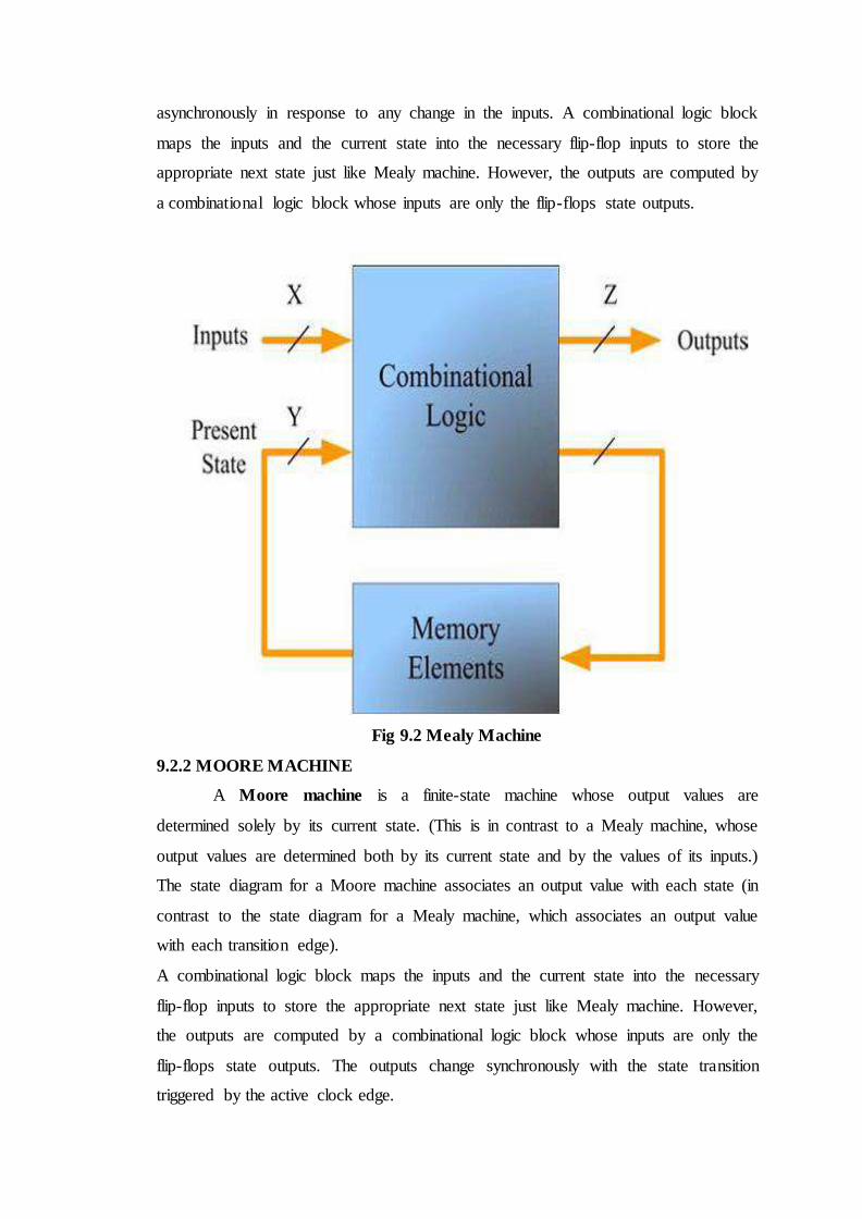
asynchronously in response to any change in the inputs. A combinational logic block
maps the inputs and the current state into the necessary flip-flop inputs to store the
appropriate next state just like Mealy machine. However, the outputs are computed by
a combinational logic block whose inputs are only the flip-flops state outputs.
Fig 9.2 Mealy Machine
9.2.2 MOORE MACHINE
A Moore machine is a finite-state machine whose output values are
determined solely by its current state. (This is in contrast to a Mealy machine, whose
output values are determined both by its current state and by the values of its inputs.)
The state diagram for a Moore machine associates an output value with each state (in
contrast to the state diagram for a Mealy machine, which associates an output value
with each transition edge).
A combinational logic block maps the inputs and the current state into the necessary
flip-flop inputs to store the appropriate next state just like Mealy machine. However,
the outputs are computed by a combinational logic block whose inputs are only the
flip-flops state outputs. The outputs change synchronously with the state transition
triggered by the active clock edge.

Fig 9.3 Moore machine
9.2.3 MECHANISM
Most digital electronic systems are designed as clocked sequential systems.
Clocked sequential systems are a restricted form of Moore machine where the state
changes only when the global clock signal changes. Typically the current state is
stored in flip-flops, and a global clock signal is connected to the "clock" input of the
flip-flops. A typical electronic Moore machine includes a combinational logic chain to
decode the current state into the outputs (lambda). The instant the current state
changes, those changes ripple through that chain, and almost instantaneously the
outputs change (or don't change). There are design techniques to ensure that no
glitches occur on the outputs during that brief period while those changes are rippling
through the chain, but most systems are designed so that glitches during that brief
transition time are ignored or are irrelevant. The outputs then stay the same
indefinitely (LEDs stay bright, power stays connected to the motors, solenoids stay
energized, etc.), until the Moore machine changes state again.

9.2.4 FSM DESIGN TECHNIQUES
FSM’s can be designed in two appropriate ways.
Classical Design:
Makes use of state tables, FF excitation tables, and Karnaugh Mapping to find
FF input control logic.
VHDL Design:
Uses case statements or IF THEN ELSE statements to set the design and the
logic synthesis tools to define equation.
9.2.5 CLASSICAL DESIGN APPROACH
1. Define the actual problem.
2. Draw a state diagram (bubble) to implement the problem.
3. Make a state table. Define all present states and inputs in a binary sequence.
4. Then define the next states and outputs from the state diagram.
5. Use FF excitation tables to determine in what states the FF inputs must be to
cause a present state to next state transition.
6. Find the output values for each present state/input combination.
7. Simplify Boolean logic for each FF input and output equations and design
logic.
9.2.6 VHDL FSM DESIGN APPROACH
Uses an enumerated type to declare state variables.
Enumerated Type: A user-defined type in which all possible values of a named
identifier are listed in a type definition.
An FSM uses a CASE statement on the enumerated type state variable.
Without any doubt, we proceed with the VHDL design approach for implementation
of our design.

STATE DIAGRAM FOR TRAFFIC LIGHT CONTROLLER
Fig 9.4 State Diagram for Traffic Light Controller
We consider 2 roads opposite to each other with 5 possible states from 1 to 5.
We initially reset them, so that State S0 shows red on both signals. After a certain
time period, moving to state 1, signal on 1 side goes read and other goes green. And
again up to a certain time count, the changes to red and yellow and then moves to
state 3 where the lights change to red both. A Similar process takes place for the
remaining states.

10. TRAFFIC LIGHT CONTROLLER
IMPLEMENTATION USING FPGA
10.1 ROAD STRUCTURE
One of the busiest traffic lights in Hyderabad city, Telangana has been
identified and used as the reference model for the design. Road structure of the traffic
intersection is shown is Fig. 1. In this structure, there are six traffics, represented by
T1, T2, T3, T4, T5 and T6 to be controlled. T1 and T2 have been identified as the
main road for the first junction while T4 and T6 are for the second junction. The last
two traffic lights, T3 and T5 are the smaller roads. The traffic flows are symbolized
by the arrows in the Fig. 1.
Fig 10.1 Road Structure

10.2. TIMING SETTING
Time is an important criterion that must be set accurately and wisely, so that
any dangerous situations, for example car accident can be avoided at the intersection.
The timing settings for the TLC are as follows:
• Green
For main roads T1, T2, T4 and T6 are 32s (peak) / 16s (off-peak) while for
narrow road T3 and T5 are 16s (peak) / 8s (off-peak).
• Amber
For all roads and during both peak and off-peak are 4s.
• Red
For all roads and during both peak and off-peak are 2s.
Fig. 2 displays the control method for the TLC during peak hour. It can be
observed from this figure that the timing settings used is fixed time approach. Fixed
time method is the most popular and old method that has been widely used in most of
the TLC setting worldwide. The proposed design differs from the existing one in
terms of the timing method. Although fixed time approach is used during peak time,
alternatively during off-peak hour, inputs from sensors are used to determine the cycle
of traffic lights. When both sensors (Sensor 1 and Sensor 2) are activated, the cycles
are the same as Fig. 2 except that timing for green light will be less: for T1, T2, T4
and T6 the setting is 16s while for T3 and T5 it will be reduced to 8s.
Fig 10.2 The control scheme (fixed-time) during peak hour
At a condition where only Sensor 1 is being set off, other cycles are the same as in

Figure 2 except that T3 and T5 cycle will be replaced by T3 and T6, and both will
turn green for 8s. When only Sensor 2 is triggered, cycles are similar to that during
only Sensor 1 is activated except that in the last cycle flow, T2 and T5 will turn green
instead of T3 and T5. At a time when both sensors are not activated, the cycles for T3
and T5 will be skipped.
10.3 VHDL MODEL
Fig. 3 shows the VHDL model of the controller. The model consists of:
CLOCK: System clock.
RESET: System reset.
PEAK: Represents peak hour (1) and off-peak hour (0)
OUTPUT (17 DOWNTO 0): All represents the six traffic lights (time three
different output combination) that the system is going to control.
SENSOR1 and SENSOR2: Represent the two sensors used to detect the
presence of car at the narrow road, T3 (Sensor1) and T5 (Sensor2).
In terms of system implementation, the approach is to develop a low cost, high
efficiency TLC system. El-Medany and Hussain suggested every intersection to be
equipped with sensors. In contrast, this system only requires sensors to be present at
the small roads where the traffic is not heavy thus reducing significant amount of
component needed. However, this system is not solely dependent on the sensor input,
as it is also equipped with a clock that is used to set the “peak hour”. This is the
period where both sensors will be temporarily disabled and the traffic is controlled by
a fixed-time system. This allows for many possible customization of the system to suit
various traffic conditions in different types of intersection. In comparison, Liu and
Chen have designed a TLC system using six timers and two specials for a very
specific scenario. This system has the advantage in terms of flexibility and can be
applied to various intersections with different traffic conditions.

11. SOURCE CODE
module tlc(
input peak,clk,rst,sen1,sen2,
output reg [2:0]t1,
output reg [2:0]t2,
output reg [2:0]t3,
output reg [2:0]t4,
output reg [2:0]t5,
output reg [2:0]t6
);
reg [2:0]state;
reg [4:0]count;
/////////////states declaration/////////
parameter s0=3'b000;
parameter s1=3'b001;
parameter s2=3'b010;
parameter s3=3'b011;
parameter s4=3'b100;
parameter s5=3'b101;
parameter s6=3'b110;
parameter s7=3'b111;
////////timer declaration//////////
parameter sec32=5'd32;
parameter sec16=5'd16;
parameter sec8=5'd8;
parameter sec5=5'd5;
parameter sec3=5'd3;

always @ (posedge clk or negedge rst)
begin
if(~rst)
begin
state<=s0;
count<=0;
end
else
case(state)
s0:if(count<sec3)
begin
state<=s0;
count<=count+1;
end
else
begin
state<=s1;
count<=0;
end
s1:if(peak==1)
begin
if(count<sec32)
begin
state<=s1;
count<=count+1;
end
else if (sen1==1)
begin
state<=s2;
count<=0;
end
else if (sen2==1)
begin

state<=s5;
count<=0;
end
else
begin
state<=s1;
count<=0;
end
end
else
begin
if(count<sec16)
begin
state<=s1;
count<=count+1;
end
else if (sen1==1)
begin
state<=s2;
count<=0;
end
else if (sen2==1)
begin
state<=s5;
count<=0;
end
else
begin
state<=s1;
count<=0;
end
end
s2:if(count<sec5)

begin
state<=s2;
count<=count+1;
end
else
begin
state<=s3;
count<=0;
end
s3:if(peak==1)
begin
if(count<sec16)
begin
state<=s3;
count<=count+1;
end
else if (sen2==1)
begin
state<=s4;
count<=0;
end
else
begin
state<=s1;
count<=0;
end
end
else
begin
if(count<sec8)
begin
state<=s3;
count<=count+1;

end
else if (sen2==1)
begin
state<=s4;
count<=0;
end
else
begin
state<=s1;
count<=0;
end
end
s4:if(count<sec5)
begin
state<=s4;
count<=count+1;
end
else
begin
state<=s6;
count<=0;
end
s5:if(count<sec5)
begin
state<=s5;
count<=count+1;
end
else
begin
state<=s6;
count<=0;
end

s6:if(peak==1)
begin
if(count<sec16)
begin
state<=s6;
count<=count+1;
end
else
begin
state<=s7;
count<=0;
end
end
else
begin
if(count<sec8)
begin
state<=s6;
count<=count+1;
end
else
begin
state<=s7;
count<=0;
end
end
s7:if(count<sec5)
begin
state<=s7;
count<=count+1;
end

else
begin
state<=s1;
count<=0;
end
default:state<=s0;
endcase
end
always @ (*) ////consider 3bit input as RYG////
///if R is active R=100//////if Y is active
Y=010///
begin ///if G is active G=001//////
case(state)
s0:begin
t1=3'b000;t2=3'b000;
t3=3'b000;t4=3'b000;
t5=3'b000;t6=3'b000;
end
s1:begin
t1=3'b001;t2=3'b001;
t3=3'b100;t4=3'b001;
t5=3'b100;t6=3'b001;
end
s2:begin
t1=3'b010;t2=3'b010;
t3=3'b100;t4=3'b010;
t5=3'b100;t6=3'b001;

end
s3:begin
t1=3'b100;t2=3'b100;
t3=3'b001;t4=3'b100;
t5=3'b100;t6=3'b001;
end
s4:begin
t1=3'b100;t2=3'b100;
t3=3'b010;t4=3'b100;
t5=3'b100;t6=3'b010;
end
s5:begin
t1=3'b010;t2=3'b001;
t3=3'b100;t4=3'b010;
t5=3'b100;t6=3'b010;
end
s6:begin
t1=3'b001;t2=3'b001;
t3=3'b100;t4=3'b100;
t5=3'b001;t6=3'b100;
end
s7:begin
t1=3'b100;t2=3'b001;
t3=3'b100;t4=3'b100;
t5=3'b010;t6=3'b100;
end
endcase
end
endmodule

12. RESULTS
12.1 RTL SCHEMATIC:
Fig 12.1: RTL Schematic

Fig 12.2: RTL Schematics with 5 Counters, Adder, D Flip-flop, 4 Comparators,
Inverter, FSM

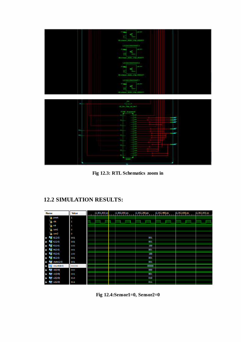
Fig 12.3: RTL Schematics zoom in
12.2 SIMULATION RESULTS:
Fig 12.4:Sensor1=0, Sensor2=0

Fig 12.5: Sensor1=0, Sensor2=1
Fig 12.6: Sensor1=1, Sensor2=0
Fig 12.7: Sensor1=1, Sensor2=1

13. FEATURES
13.1 ADVANTAGES
Speed of operation.
Low power consumption.
Easy to implement.
Less area.
Less wiring complexity.
13.2 APPLICATIONS
Ease to control the traffic signals at any junction by using Intelligent Transport
System (ITS) by using Field Programmable Gate Array (FPGA).The code is written
in Verilog HDL design pattern and synthesis is done in XILINX of version 14.5.
13.3 PAST TECHNOLOGIES AND THIER DRAWBACKS
13.3.1 USING MICROCONTROLLER
Present Traffic Light Controller (TLC) is based on microcontroller and
microprocessor. These TLC have limitations because it uses the pre-defined hardware,
which is functioning according to the program that does not have the flexibility of
modification on real time basis. Due to the fixed time intervals of green, orange and
red signals the waiting time is more and car uses more fuel. FPGA has many
advantages over microcontroller, some of these advantages are; the speed, number of
input/output ports and performance which are all very important in TLC design, at the
same time ASIC design is more expensive than FPGA. Most of the TLCs
implemented on FPGA are simple ones that have been implemented as examples of
FSM. This paper concerned with an FPGA design implementation of a low cost 24-
hour advanced traffic light controller system that was built as a project of a VLSI
design subject using VHDL.
13.3.2 USING PLD AND CPLD
Traffic Light Control System (TLC) system can be designed on GAL (Generic
Array Logic) using Programmable Logic Device (PLD) using Complex
Programmable Logic Device (CPLD). For PLD implementation, we consider GAL

(16V8) chips, which can be reprogrammed and erased. For the CPLD implementation,
we consider FPGA (ALTERA's Flex 10k family's EPF10K10TC144-4) chip, which is
a 144 pin SRAM. The CPLD design was developed using the CPLD programming
software MAX PLUS2 v 9.23. The traffic light controller consists of traffic signals
(Red, Yellow/Amber & Green). We have designed the traffic controller using both
CPLD and PLD. Then we have taken the real time waveform as well as the simulated
waveform for different frequencies. The Digital Storage Oscilloscope (DSO).was
used to generate the real time wave from the traffic controllers. The results from the
real time waveform clearly illustrates that CPLD has the better performance over the
PLD technology. In this power consumption is high and circuitry becomes complex
with number of PLD and CPLD’s. We are using a FPGA which consists of CLB by
which the power consumption is lessened and circuitry also becomes simple.
13.4 FUTURE ENHANCEMENT
For future works, the TLC design will include pedestrian crossing lights with
the intention that the reliability of the design can be much enhanced. Lastly, a
comprehensive and an exceptional TLC design can be made into an embedded circuit
board to control the actual traffic flow in the city’s traffic intersections.

14. CONCLUSION
An FPGA design of TLC with six traffic lights has been simulated using
Quartus II, implemented and tested using ALTERA FLEX10K chip. One of the
advantage of this design over the existing method is the waiting time of driver during
off-peak hour has been reduced, means that the normal design cycle (using fixed-time
technique) has been reduced notably, thus ameliorate reliability and flexibility of the
TLC.
An FPGA design of a 24-hour traffic light controller system of a twelve roads
structure with six traffic lights has been simulated, implemented and tested. The
system has been designed using VHDL, and implemented on hardware using XILINX
Spartan 3E and Virtex 5xc5vlx110t FPGA kit. The functionality of this design can be
easily enhanced.
Some of these functions are to control more than 6 traffic lights. Also, to allow
the user to assign the time for each traffic light (i.e., minimum time to be Green),
adding more sensors on each road to count the number of cars in each road and check
for the longer queue to increase the timer for that road. Here we have manually
entered the signals for the NS car and EW car since the sensor interfacing is not done
at yet manually entered the signals for the Ns car and EW car since the sensor
interfacing is not done yet which remains as future scope as well as the camera
interfacing which will detect if any car breaks the traffic rule serve as a security
purpose and emergency services.

15. REFERENCES
El-Medany, W.M., & Hussain, M.R. (2007) FPGA-Based Advanced Real
Traffic Light Controller System Design.
Proceeding of 4th IEEE International Workshop on Intelligent Data
Acquisition and Advanced Computing Systems: Technology and
Applications, ISBN: 978-1-4244-1347-8, pg. 100 – 105.
Chan, S.S., Deshpande, R.S. & Rana, J.G. (2009) Design of Intelligent
Traffic Light Controller Using Embedded System.
Proceeding of 2nd International Conference on Emerging Trends in
Engineering and Technology, ISBN: 978-1-4244-5250-7, pg. 1086-1091
Liu, Y. & Chen. X. (2009) Design of Traffic Lights Controlling System Based on
PLC and Configuration Technology.
Proceeding of International Conference on Multimedia Information Networking
and Security 2009, ISBN: 978-0-7695-3843-3, pg. 561-563
Kulkarni, G.H. & Waingankar, P.G. (2007) Fuzzy logic based traffic light
controller.
Proceeding of International Conference on Industrial and Information Systems
2007, ISBN: 978-7-4244-1151-1, pg. 107-110
Norhuzaimin, J. & Maimun, H.H. (2005) The Design of High Speed UART.
Proceeding of Asia Pacific Conference on Applied Electromagnetics, ISBN 0-
7803-9431-3, pg. 306-310.
STEPHEN BROWN, JONATHAN ROSE, “FPGA and CPLD architectures: A
Tutorial,” Design & Test of Computers, IEEE, Volume 13, Issue 2, summer 1996
Page(s):42 – 57.
CPLD Logic Design and Practices (LP 2900 manual)
Wikipedia, “Programmable Logic device,”
http://en.wikipedia.org/wiki/Programmable_logic_device.
Wikipedia, “Traffic light,”
http://en.wikipedia.org/wiki/Traffic_light.
Charles H. Roth, Jr. “Digital Systems Design Using VHDL”.