design of heuristic algorithms based on shannon expansion for low-power logic circuit synthesis
TRANSCRIPT

Design of heuristic algorithms based on Shannon expansion for low-power logic circuit synthesis
H.Kim I.S.Choi S.Y. Hwang
Indexing terms: Low-power design, Shannon expansion, Switching activity, Logic synthesis
Abstract: A pair of heuristic algorithms based on Shannon expansion are proposed for the synthesis of low-power combinational circuits. Selecting an input variable for a given function, the bipartitioning algorithm performs Shannon expansion with respect to a selected variable to reduce the power dissipation of the subcircuit implementing the cofactor. The multiple partitioning algorithm partitions a given circuit into several subcircuits such that only a subcircuit can be activated at a time to reduce unnecessary signal transitions. In the algorithm, a circuit is recursively partitioned by applying Shannon expansion as long as power consumption is reduced. Experimental results for the MCNC benchmarks show that the bipartitioning and multiple partitioning algorithms based on Shannon expansion are effective by generating circuits consuming 39.1 and 50.5% less power on the average, respectively, when compared to the conventional algorithm based on precomputation logic.
1 Introduction
With the increasing use of portable communication and computing devices, power dissipation has emerged as an important design parameter in the design of porta- ble computing applications. Low-power design is needed to extend battery life and to reduce packaging and cooling cost which is growing as the operating speed and density of VLSI circuits increase. Low-power design can be achieved at various levels of design hier- archy: system level, architectural level, gate level and device level. Several techniques have been proposed to reduce the power requirements of combinational and sequential logic circuits [l-31. Most of these researches in gate level have focused on reducing internal switch- ing activities, observing that the average power con- sumed by a CMOS gate is dependent on the switching 0 IEE, 1997 IEE Proceedings online no. 19971481 Paper first received 10th September 1996 and in final revised form 23rd May 1997 The authors are with the CAD and Computer Systems Laboratory, Department of Electronic Engineering, Sogang University, CPO Box 1142, Seoul 100-611, Korea
activities of the gate outputs [4-61. The ‘don’t-care’ optimisation method tries to reduce switching activities and power dissipation by utilising a ‘don’t-care’ set [5]. A path balancing technique eliminates spurious transi- tions which account for between 10 and 40% of dynamic power dissipation in combinational logic cir- cuits [7]. To reduce spurious transitions the delays of different paths converging at a gate are made equal by inserting unit-delay buffers to the inputs of gates selec- tively. However, the addition of buffers increases capacitance, which may offset the reduction in switch- ing activities. Factorisation is a method of technology- independent multilevel optimisation performed to reduce the areas for the gates implementing a given function. A modified kernel extraction algorithm to reduce switching activities in a circuit is described in
The precomputation logic scheme is based on selec- tively precomputing the output logic values of the cir- cuit one clock cycle before they are required, and using the precomputed values to reduce internal switching activities in the succeeding clock cycle [9]. Conse- quently, the power dissipation of the entire circuit is reduced. Alidina et al. proposed an algorithm which generates precomputation logic block using observabil- ity don’t care (ODC) sets [9, 101. However, it is not always possible to find an appropriate ODC for the precomputation logic, and an area overhead for the precomputation logic is not negligible. Lucian0 and McGeer proposed the circuit structure based on Shan- non expansion to reduce power dissipation [ll]. In the scheme, the BDD is initially constructed for the given circuit and then the BDD nodes are mapped into logic gates. The Shannon circuit can reduce power consump- tion by minimising signal transitions. However, the circuit has area and delay overheads inherent in its structure. Multiplexor-based Shannon expansion scheme is a variant of the precomputation scheme in which a circuit is transformed into two cofactor circuits by applying Shannon expansion with respect to a selected input variable [9, 121. Power reduction is achieved by disabling a subcircuit which does not con- tribute to the output evaluation.
In this paper, a pair of heuristic algorithms are pre- sented. First, a bipartitioning algorithm based on Shan- non expansion (BPSE) is proposed for choosing a control variable to select a proper output among cofac- tor subcircuits. In the proposed algorithm the control variable is selected by observing the structure of a func- tion without exhaustive evaluation of the cofactor sub-
PI.
IEE ProcCircuits Devices Syst., Vol. 144, No. 6, December 1997 355

circuits to find the circuit consuming the least power. Next, a multiple partitioning algorithm based on Shan- non expansion (MPSE) is proposed together with its architecture. By the MPSE algorithm, a given circuit is transformed into a structure containing multiple subcir- cuits, input latches, and an output multiplexor by recursive application of Shannon expansion.
2 Power dissipation model of CMOS circuits
The average power consumption of a CMOS gate is given by eqn. 1
Pavg = Pswztchzng + PshoTt-czTcuzt + 8 e a k a g e
1 1 2Tc TC
= - N C V ~ D + -NQ,,VDD + I iearcV~~
(1) where V,, is the supply voltage and Tc is the clock period. The first term Pswitchzng is the switching activity power required to charge and discharge circuit nodes. Load capacitance is represented by C and the factor N is the average number of switching per clock cycle at the gate output. The second term Pshortclrcurt is the power dissipation due to the current from the supply to ground during input transitions, called short-circuit current. The factor Q,, denotes the quantity of charge carried by the short-circuit current during a transition at the output. The third term Pleukuge is the static power dissipation due to the leakage current Ileuk. Since the power dissipation due to switching activities accounts for over 90% of the average power consumption, only the power factor of switching activities is taken into consideration in modelling the power dissipation of CMOS circuits [5]. The average power dissipation in a CMOS circuit is proportional to the transition proba- bility, the probability that a signal switches from one state to another in a node [13, 141. Accordingly, the average switching activity power of a CMOS circuit is modelled as in eqn. 2
n
where Ci is the load capacitance of the node xi, and pt(xi) is the transition probability at the node xi. The power dissipation by spurious transitions which arise from unbalanced delay paths of the circuits is not included in eqn. 2. The equation represents the dynamic power arising from charging and discharging circuit nodes.
3 Shannon expansion schemes
3.7 Shannon expansion scheme A function f(il, i2, ..., in) can be Shannon expanded with respect to an input variable il as f = ilJI, + c f ~ , where f i , and fq are the cofactors o f f for il and i,, respectively. A combinational circuit can be transformed into a Shannon expansion form using two input latches and an output multiplexor as shown Fig. 1 [12]. Depending on the value of il, only one cofactor subcircuit is computed, while the other is disa- bled by maintaining the previous values stored in the input latches. The input variable il drives the select line of the multiplexor to select the cofactor subcircuit which has the correct output logic. The internal switch- ing activities of the circuit are reduced since only a fraction of the circuit responds to determine the output
-
356
value according to the control input variable. Accord- ingly, the power consumption is reduced considerably. To maximally reduce the power dissipation of the cir- cuit transformed by Shannon expansion the control variable must be properly selected among input varia- bles of a given logic function.
er Fig. 1 Circuit architecture based on Shannon expansion
3.2 Heuristic algorithm for control variable selection In the Shannon expansion scheme the size of the cofac- tor subcircuits notably depends on the input variable selected as the control signal of the mux and latches. To avoid an exhaustive search, we propose a heuristic algorithm which selects the most beneficial control var- iable among inputs of a given logic function. The heu- ristics are based on the observation that the size of the cofactor subcircuits for a selected input is inversely proportional to the number of appearances of the vari- able in the cubic representation of a given circuit. The algorithm is summarised as follows. First, the algo- rithm collapses a given logic function f into the cubic representation. The number of variables for each cube is calculated to select the variable which most fre- quently appears in cubes. For the unate variable, the weight of the variable becomes the number of cubes containing the variable. For the binate variable, the proposed algorithm computes the weight of the varia- ble by summing the number of cubes containing the variable or its complement. If only one variable in the function f has the maximum weight, this variable is selected as a control variable. When performing the Shannon expansion with respect to the selected varia- ble, the cofactors of the selected variable have the min- imal set of literals. This produces minimum-sized subcircuits and leads to the reduction in power dissipa- tion. If more than one variable has the maximum weight, the proposed algorithm figures out the number of literals for each cube containing the variables by cal- culating the number of variables contained in the cube, then selects the variable with the largest value as the optimal input variable. By this proposed heuristic, the gates with large fan-ins are removed in the subcircuits, and hence the reduction in power consumption can be achieved. The outline of the proposed algorithm for multiple-output functions is shown in Fig. 2.
For example, a logic function f = i5 (< + i3i6) + (i2< + <i3)(5i4f il (i4< + cis)) is collapsed to f = <is + i3i5i6 + ili2i3i4 + <Gi3i4 + ili2<i4G + ili2qi& + ilGi3i4< + il6i3Gi5. The weights of variables il, i2, i3, i4, if(, i6 are 7, 6, 7, 6, 5, 1. Since the variables il and i3 have the same weight, we sum the numbers of literals in cubes containing il and i3. The figures for il and i3 are 30 and 3 1, respectively. According to the second heuristic i3 is selected as the control variable.
IEE Proc -Circuits Devices Syst , Vol 144, No 6, December 1997

~~~ ~ ~~~
Control_ Vnrinble-Selection ( F = { f,. ..., J,? } ) I* F : a given multiple-output function * I I* Num-Cubes : number of cubes containing each literal in the function F */ /* Num-Variables : iiuinber of variables contained in the cube ofthe set 'Cubes' */ (
perform collapsing for the fiinction F ; for each variable v, in F {
/* Compute the weight of each variable * I Weight( v,) = Num_Cubes( v, ) + Num-Cubes( if ( oiily one variable v, i n the function has maximum weight)(
}
);
v = L', ;
else( for each variable v i with the same weight{
Weight( v, ) = 0: Cubes = set of cubes containing vj; for each cube c E Cubes
Weight( vi ) = Weight( Y, ) + Num-Variables(c);
}
I
return(v); v = the variable with maximum weight;
}
Fig. 2 Algorithm for control variable selection
Since the previous algorithms based on precomputa- tion logic require an additional circuit for precomputa- tion which causes to increase path delay, they must be applied to a noncritical circuits. However, the architec- ture based on the Shannon expansion scheme does not need precomputation logic. Also, the bipartitioning algorithm based on Shannon expansion is not required to extract ODC from a logic network while the precomputation logic scheme needs to construct the precomputation logic predicting output value.
I
Fig.3
1-1, - I I , \' ~
1L1 I
f /'
0 0 0
fN
r /
selection : L . Logic
I.
, r Log 2N1
Multipartitioned circuit structure obtained by MPSE algorithm
3.3 Multiple partitioning algorithm based on Shannon expansion The Shannon expansion scheme which partitions a given circuit into two disjoint subcircuits (BPSE algo- rithm) effectively reduces power dissipation of a logic circuit, when a control variable is properly chosen. However, the total size of the two subcircuits may become much greater than that of the original circuit, since a logic part is to be duplicated when a logic func- tion is cofactored into two subfunctions by applying Shannon expansion. If the Shannon expansion is applied to simple logic circuits, it is a trivial problem but it is not so for complex logic circuits. By applying Shannon expansion recursively with respect to a set of
IEE Proc.-Circuits Devices Syst., Vol. 144, No. 6, December 1997
input variables, a logic function can be partitioned into several subcircuits. The multiple partitioned logic func- tions may contain less duplicated logic gates than the bipartitioned logic functions. The circuit structure obtained by the proposed multiple partitioning algo- rithm based on Shannon expansion (MPSE algorithm) is shown in Fig. 3. In the Figure, I = {il, iz, ..., in} is the set of primary input variables, and Is is a subset of the inputs used in the selection logic, which is referred to as the control input set. The selection logic is con- structed in the form of a decoder. The function of the selection logic is to activate a subcircuit by enabling its input latch according to the inputs selected as a control input set. The output of the selection logic drives the select line of the output mutiplexor. Only a subcircuit is activated by setting the load-enable signal of input latches.
The proposed MPSE algorithm partitions a given cir- cuit into multiple subcircuits. First, it partitions a given circuit info two subcircuits using the procedure Con- trol-Variable-Selection described in Section 3.2. The partitioned subcircuits are stored in a priority queue according to their estimated power dissipations. From the priority queue, a subcircuit having the largest power consumption is popped and partitioned and is replaced by the partitioned circuits, provided that the overall power dissipation is reduced. This process is repeated until no more power reduction is achieved. If the partitioning process is iterated n times, the given circuit is partitioned into n + 1 subcircuits and needs rlog(n + 1)1 inputs to properly activate a subcircuit selectively. The outline of the proposed algorithm is described in Fig. 4.
LP-Synthesis ( C ) /* C : a given circuit /* V : variable selected as control signal /* Q : priority queue /* S : set of partitioned circuits {
*/
*/ */
*/
s = 4; v = 4: Q = Push ( C ): P, = estimated power for C;
while ( Q is iiot empty ) { C = pop a circuit from Q; V = Control_ Vuriuble-Selection ( C ); ( C1, C2 ) = partition C by Shannon expansion with respect to V; ( 4 , ,< , )= estimated power for ( C1, C2 );
i f ( e., + 4.. < Pc)
Pus11 (C I, 4, ), (C2, I: , 011 Q;
S = S u ( C . 4 ) ; else
1
Generate result circuits from S: }
Fig.4 Multiple partitioning algorithm
A logic part of an MCNC benchmark circuit 'major- ity' is shown in Fig. 5, which is optimised by SIS 1.2 using rugged script [15]. When the input variables are assumed to be equiprobable, power consumption is 64pW. Figs. 6 and 7 show the circuits transformed by precomputation logic optimisation [9, 101 and the BPSE algorithm, respectively. The power dissipation of the circuit obtained by precomputation logic scheme is
357

39pW, while that by the BPSE algorithm is 28pW. The circuit in Fig. 8 which is obtained by applying the MPSE consumes 19pW. It shows a significant improve- ment in power reduction.
n
f
Fig. d+=----- 5 An example combinational circuit
a
C e f
. . . , , . . . . . . , . ..,..,... ... precomputation Logic
Fig. 6 Circuit obtained by precomputation logic scheme
f
Fig.7 Circuit obtained by BPSE algorithm
4 Experimental results
L1 d - -
1 - I 1
C e
f
a b
Fig.8 Circuit obtained by MPSE algorithm
1.2 system for area optimisation, precomputation-based scheme, and two proposed algorithms (BPSE and MPSE algorithms). Experimental results for the circuits obtained by precomputation-based scheme was achieved by using the precomputation package in SIS [9]. The power measurements were made at a clock fre- quency of 20MHz and a supply voltage of 5V using the zero-delay model by the power estimation function of SIS. In the measurements, the power consumed by the input latches is not included, since only a few latches are activated and the contributions by the input latches to the overall power consumption are negligible.
Table 1: Statistics of benchmark circuits optimised for area by SIS
Power (PW) Circuits ins outs lits
b l
cht
cmb
cm42a
cm 138a
cm 150a
count
decod duke2
e64
majority
misex2
m ux
pcle
pcler8
sa02
sct
unreg
3 4 23 45
47 36 261 526
16 4 94 620
4 10 42 111
6 8 48 87
21 1 716 212
35 16 213 588
5 16 62 105 22 29 698 1270
65 65 383 348
5 1 23 64
25 18 178 363
21 1 118 234
19 9 109 692 27 17 187 283
10 4 290 61 1
19 15 117 319
36 16 216 1499
x2 10 7 68 228
z4m 1 7 4 55 208
C5315 178 123 2094 7 205
and integrated in SILOS-I1 [16]. Experiments were per- c6228 32 32 4775 12034
formed with four different optimisation methods: SIS U 5 5 2 207 208 5170 13633
The proposed algorithms have been implemented in C
358 IEE Pvoc.-Civcuits Devices Syst., Vol. 144, No. 6, December 1997
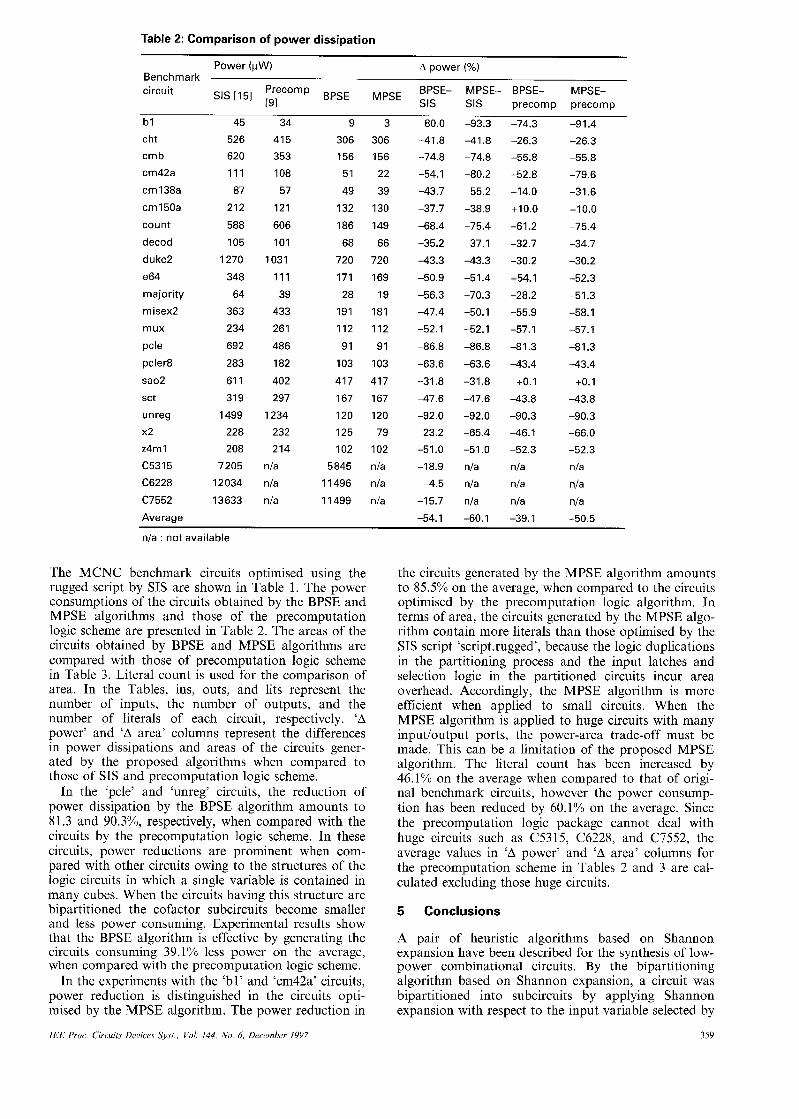
Table 2: Comparison of power dissipation
Power (pW) A power (%) Benchmark
BPSE- MPSE- BPSE- MPSE- BPSE MPSE s,s SIS precomp precomp
circuit SIS [I51 :rmp b l
cht
cmb
cm42a
cm 138a
cm 150a
count
decod
duke2
e64
majority
misex2
m ux
pcle
pcler8
sa02
SCt
unreg
x2
z4ml
C5315
C6228
C7552
Average
45
526
620
111
87
212
588
105
1270
348
64
363
234
692
283
61 1
319
1499
228
208
7205
12 034
13 633
34
415
353
108
57
121
606
101
1031
111
39
433
261
486
182
402
297
1234
232
214
nla
nla
nla
9 3
306 306
156 156
51 22
49 39
132 130
186 149
68 66
720 720
171 169
28 19
191 181
112 112
91 91
103 103
417 417
167 167
120 120
125 79
102 102
5845 n/a
11496 n/a
11499 nla
-80.0 -93.3 -74.3 -91.4 -41.8
-74.8
-54.1
-43.7
-37.7
-68.4
-35.2
-43.3
-50.9
-56.3
-47.4
-52.1
-86.8
-63.6
-31.8
4 7 . 6
-92.0
-23.2
-51.0
-18.9
-4.5
-15.7
-54.1
-41.8
-74.8
-80.2
-55.2
-38.9
-75.4
-37.1
-43.3
-51.4
-70.3
-50.1
-52.1
-86.8
-63.6
-31.8
-47.6
-92.0
-65.4
-51.0
nla
nla
nla
-60.1
-26.3
-55.8
-52.8
-14.0
+10.0
-61.2
-32.7
-30.2
+54.1
-28.2
-55.9
-57.1
-81.3
-43.4
+o. 1
-43.8
-90.3
-46.1
-52.3
nla
nla
nla -39.1
-26.3
-55.8
-79.6
-31.6
+10.0
-75.4
-34.7
-30.2
-52.3
-51.3
-58.1
-57.1
-81.3
-43.4
+o. 1
-43.8
-90.3
-66.0
-52.3
nla
nla
nla
-50.5
n/a : not available
The MCNC benchmark circuits optimised using the rugged script by SIS are shown in Table 1. The power consumptions of the circuits obtained by the BPSE and MPSE algorithms and those of the precomputation logic scheme are presented in Table 2. The areas of the circuits obtained by BPSE and MPSE algorithms are compared with those of precomputation logic scheme in Table 3. Literal count is used for the comparison of area. In the Tables, ins, outs, and lits represent the number of inputs, the number of outputs, and the number of literals of each circuit, respectively. ‘A power’ and ‘A area’ columns represent the differences in power dissipations and areas of the circuits gener- ated by the proposed algorithms when compared to those of SIS and precomputation logic scheme.
In the ‘pcle’ and ‘unreg’ circuits, the reduction of power dissipation by the BPSE algorithm amounts to 81.3 and 90.3%, respectively, when compared with the circuits by the precomputation logic scheme. In these circuits, power reductions are prominent when com- pared with other circuits owing to the structures of the logic circuits in which a single variable is contained in many cubes. When the circuits having this structure are bipartitioned the cofactor subcircuits become smaller and less power consuming. Experimental results show that the BPSE algorithm is effective by generating the circuits consuming 39.1% less power on the average, when compared with the precomputation logic scheme.
In the experiments with the ‘bl’ and ‘cm42a’ circuits, power reduction is distinguished in the circuits opti- mised by the MPSE algorithm. The power reduction in
IEE Proc.-Circuits Devices Syst., Vol. 144, No. 6, December 1997
the circuits generated by the MPSE algorithm amounts to 85.5% on the average, when compared to the circuits optimised by the precomputation logic algorithm. In terms of area, the circuits generated by the MPSE algo- rithm contain more literals than those optimised by the SIS script ‘script.rugged’, because the logic duplications in the partitioning process and the input latches and selection logic in the partitioned circuits incur area overhead. Accordingly, the MPSE algorithm is more efficient when applied to small circuits. When the MPSE algorithm is applied to huge circuits with many input/output ports, the power-area trade-off must be made. This can be a limitation of the proposed MPSE algorithm. The literal count has been increased by 46.1% on the average when compared to that of origi- nal benchmark circuits, however the power consump- tion has been reduced by 60.1% on the average. Since the precomputation logic package cannot deal with huge circuits such as (25315, C6228, and C7552, the average values in ‘A power’ and ‘A area’ columns for the precomputation scheme in Tables 2 and 3 are cal- culated excluding those huge circuits.
5 Conclusions
A pair of heuristic algorithms based on Shannon expansion have been described for the synthesis of low- power combinational circuits. By the bipartitioning algorithm based on Shannon expansion, a circuit was bipartitioned into subcircuits by applying Shannon expansion with respect to the input variable selected by
359
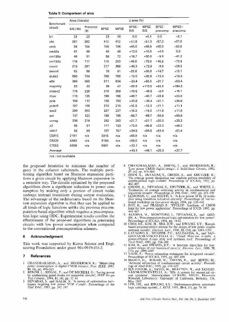
Table 3: Comparison of area
Area (literals) A area (%)
SIS [I51 [91
Benchmark circuit Precomp BPSE- MPSE- BPSE- MPSE-
BPSE MPSE SIS SIS precomp precomp
b l
cht
cmb
cm42a
cm 138a
cml50a
count
decod
duke2
e64
majority
misex2
mux
pcle
pcler8
sa02
sct
u n reg
x2
23
261
94
42
48
116
213
62
698
383
23
178
118
109
187
290
117
216
68
23
262
104
46
51
117
29 1
68
704
388
23
225
135
112
189
302
122
218
91
23 24
412 412
156 156
48 46
56 72
170 203
317 368
78 81
789 789
511 634
39 47
219 259
166 166
158 153
210 210
227 227
195 195
262 262
117 133
0.0
+57.9
+66.0
+13.0
+16.7
+46.6
+48.3
+25.8
+13.0
+33.4
+69.5
+23.0
+40.7
+45.0
+12.3
+16.2
+66.7
+21.7
+72.0
+0.1 0.0
+57.3 +57.3
+66.0 +50.0
+10.0 +4.0
+50.0 +9.8
+75.0 +45.2
+72.8 +9.0
+30.6 +14.7
+30.6 +13.4
+65.5 +31.7
+113.0 +62.5
+45.5 -3.0
+40.7 +23.0
+40.4 +41.1
+12.3 +11.1
+16.2 +11.6
+66.7 +59.8
+21.7 +20.2
+95.6 +22.2
+0.1
+57.9
+50.0
0.0
+41.2
+73.5
+26.5
+19.1
+13.4
+63.4
+104.2
+15.1
+23.0
+36.6
+11.1
+11.6
+59.8
+20.2
+46.2
z4m 1 55 59 107 107 +94.5 +94.5 +81.4 +81.4
C5315 2191 n/a 3816 n/a +88.8 nla nla nla
C6228 4864 n/a 9194 n/a +89.0 n/a n/a n/a
C7552 6509 n/a 8601 n/a +32.1 n/a n/a n/a Average +43.1 +46.1 +28.3 +37.7
n/a : not available
the proposed heuristics to minimise the number of gates in the cofactor subcircuits. The multiple parti- tioning algorithm based on Shannon expansion parti- tions a given circuit by applying Shannon expansion in a recursive way. The circuits optimised by the proposed algorithms show a significant reduction in power con- sumption by making only a portion of circuit nodes undergo internal transitions during output evaluation. The advantage of the architectures based on the Shan- non expansion algorithm is that they can be applied to all kinds of logic functions unlike the previous precom- putation-based algorithm which requires a precomputa- tion logic using ODC. Experimental results confirm the effectiveness of the proposed algorithms in generating circuits with low power consumption when compared to the conventional precomputation schemes.
6 Acknowledgment
This work was supported by Korea Science and Engi- neering Foundation under grant 961-0919-101-2.
7 References
CHANDRAKASAN, A., and BRODERSEN, R.: ‘Minimizing power consumption in digital CMOS circuits’, Proc. IEEE, 1995, 83, (4), pp. 498-523 BENINI, L., SIEGAL, P., and DE MICHELI, G.: ‘Saving power by synthesizing gated clocks for sequential circuits’, IEEE Design Test Comput., 1994, 11, (4), pp. 3241 DEVADAS, S., and MALIK, S.: ‘A survey of optimization tech- niques targeting low power VLSI circuits’. Proceedings of the 32nd DAC, 1995,pp.242-247
4 CHANDRAKASAN, A., SHENG, T., and BRODERSEN, R.: ‘Low power CMOS digital design’, J. Solid-state Circuits, 1992, 27, (4), pp. 473484
5 SHEN, A., DEVADAS, S., GHOSH, A., and KEUTZER, K.: ‘On average power dissipation and random pattern testability of combinational logic circuits’. Proceedings of ICCAD, 1992, pp. 402407
6 GHOSH, A., DEVADAS, S., KEUTZER, K., and WHITE, J.: ‘Estimation of average switching activity in combinational and sequential circuits’. Proceedings of 29th DAC, 1992, pp. 253-259
7 LEMONDS, C., and SHETTI, S.: ‘A Low power 16 by 16 multi- plier using transition reduction circuitry’. Proceedings of interna- tional workshop on Low-power design, 1994, pp. 139-142
8 ROY, K., and PRASAD, S.: ‘SYCLOP: Synthesis of CMOS logic for low power application’. Proceedings of ICCD, 1992, pp. 464467
9 ALIDINA, M., MONTEIRO, J., DEVADAS, S., and GHO- SH, A.: ‘Precomputation-based logic optimization for low power’. Proceedings of ICCAD, 1994, pp, 74-81
10 CHOI, IS., KIM, H., SEO, D.W., and HWANG, S.Y.: ‘Kernel- based precomputation scheme for the design of low power combi- national circuits’. Electron. Lett.. 1996. 32. (14). DD. 1281-1283
11
12
LAVAGNO, L.,’MCGEER, P.C., SALDANHA:A., and SAN- GIOVANNI-VINCENTELLI, A.: ‘Timed Shannon circuits: a power-efficient design style and synthesis tool’. Proceedings of 32nd DAC, 1995, pp. 254-260 KIM, H., and HWANG, S.Y.: ‘A heuristic algorithm for low- power design of combinational circuits’, Electron. Lett., 1996, 32, (12). nn. 1066-1067 , j I I ~ ~ ~ ~
13 NAJM, F.: ‘Power estimation techniques for integrated circuits’. Proceedings of ICCAD, 1995, pp. 492499
14 MEHTA, H., BORAH, M., OWENS, R., and IRWIN, M.: ‘Accurate estimation of combinational circuit activity’. Proceed- ings of 32nd DAC, 1995, pp. 618-622
15 SENTOVICH, E., SAVOJ, H., BRAYTON, R., and SANGIO- VANNI-VINCENTELLI, A.: ‘SIS: A system for sequential cir- cuit synthesis’. Memorandum UCB/ERL M92/41, Electronic Research Laboratory, University of California, Berkeley, CA, May 1992
16 LEE, J.H., and HWANG, S.Y.: ‘Performance-driven automatic logic synthesis system’, J. KITE, 1991, 28-A, (l), pp. 74-84
360 IEE Proc.-Circuits Devices Syst., Vol. 144, No. 6, December 1997