design of high speed packages and boards using …
TRANSCRIPT
DESIGN OF HIGH SPEED PACKAGES AND BOARDSUSING EMBEDDED DECOUPLING CAPACITORS
A ThesisPresented to
The Academic Faculty
by
Prathap K. Muthana
In Partial Fulfillmentof the Requirements for the Degree
Doctor of Philosophy in theSchool of Electrical and Computer Engineering
Georgia Institute of TechnologyAugust 2007
DESIGN OF HIGH SPEED PACKAGES AND BOARDSUSING EMBEDDED DECOUPLING CAPACITORS
Approved by:
Professor Madhavan Swaminathan,AdvisorSchool of Electrical and ComputerEngineeringGeorgia Institute of Technology
Dr. Mahadevan IyerSchool of Electrical and ComputerEngineeringGeorgia Institute of Technology
Professor Rao TummalaSchool of Electrical and ComputerEngineeringGeorgia Institute of Technology
Professor William A. DoolittleSchool of Electrical and ComputerEngineeringGeorgia Institute of Technology
Professor David KeezerDepartment of Electrical andComputer EngineeringGeorgia Institute of Technology
Professor Suresh SitaramanSchool of Mechanical EngineeringGeorgia Institute of Technology
Date Approved: 23 April 2007

ACKNOWLEDGEMENTS
The past few years at Georgia tech have been very eventful for me. There are a lot
of people whom I would like to acknowledge for their support and friendship without
whom this work would not have been possible.
First of all, I would like to thank my academic advisor Professor Madhavan Swami-
nathan for his advice, insight, support, enthusiasm and encouragement over the course
of my research. I am grateful for him for giving me the opportunity to work with the
Epsilon group and for being a continuous source of inspiration. I would also like to
thank my co-advisor Professor Rao Tummala for his insights and helping me in getting
a well rounded thesis. I would like to acknowledge the comments and suggestions of
my committee members Professor David Keezer, Professor Alan Doolittle, Professor
Suresh Sitaraman and Dr. Mahadevan Iyer.
Special thanks to my colleagues and friends at Georgia Tech especially Dr. Ege
Engin, Dr. Raj Pulugurtha, Venky Sundaram and Dr. Lixi Wan for their inputs to my
research. I would also like to thank all the present and past members of the Epsilon
group for their support and encouragement. My thanks to: Subraminiam Lalgudi, Sou-
vik Mukherjee, Krishna Bharath, Krishna Srinivasan, Wansuk Yun, Nevin Atlun-
yurt, Marie Milleron, Abdemanaf Tambawalla, Tae Hong Kim, Kijin Han, Abhilash
Goyal and Beranard Yang. Erdem Matoglu, Bhyrav Mutnury, Moises Cases, Daniel
de Araujo and Nam Pham at IBM for their support and input to my thesis.
I would finally like to thank my family for being a constant source of strength and
encouragement over the course of my studies.
iii
TABLE OF CONTENTS
ACKNOWLEDGEMENTS . . . . . . . . . . . . . . . . . . . . . . . . . . . . iii
LIST OF TABLES . . . . . . . . . . . . . . . . . . . . . . . . . . . . . . . . . vii
LIST OF FIGURES . . . . . . . . . . . . . . . . . . . . . . . . . . . . . . . . viii
SUMMARY . . . . . . . . . . . . . . . . . . . . . . . . . . . . . . . . . . . . . xvi
I INTRODUCTION . . . . . . . . . . . . . . . . . . . . . . . . . . . . . . 1
1.1 Power Distribution Networks . . . . . . . . . . . . . . . . . . . . . 2
1.2 Simultaneous Switching Noise . . . . . . . . . . . . . . . . . . . . . 4
1.3 Decoupling Components . . . . . . . . . . . . . . . . . . . . . . . . 7
1.4 Characteristics of Power Distribution Planes . . . . . . . . . . . . . 9
1.4.1 Effect of Dielectric Loss . . . . . . . . . . . . . . . . . . . . 10
1.4.2 Effect of Dielectric Constant . . . . . . . . . . . . . . . . . . 11
1.4.3 Effect of Dielectric Thickness . . . . . . . . . . . . . . . . . 11
1.5 Decoupling Methodologies used in today’s systems . . . . . . . . . 13
1.6 Limitations of present day decoupling methodologies and proposedsolutions. . . . . . . . . . . . . . . . . . . . . . . . . . . . . . . . . 17
1.7 Proposed Research and Dissertation Outline . . . . . . . . . . . . . 24
II PACKAGE REQUIREMENTS FOR MULTI-CORE PROCESSORS . . 29
2.1 Processor Power Dissipation Calculations . . . . . . . . . . . . . . 32
2.2 Power Dissipation Calculations . . . . . . . . . . . . . . . . . . . . 36
2.3 Analysis of multi-core processors . . . . . . . . . . . . . . . . . . . 40
2.4 Packaging Platform . . . . . . . . . . . . . . . . . . . . . . . . . . . 45
2.4.1 Package details estimation . . . . . . . . . . . . . . . . . . 46
2.4.2 Fine pitch interconnects . . . . . . . . . . . . . . . . . . . . 48
2.4.3 Microvias . . . . . . . . . . . . . . . . . . . . . . . . . . . . 49
2.4.4 Embedded Capacitors . . . . . . . . . . . . . . . . . . . . . 50
2.5 Summary . . . . . . . . . . . . . . . . . . . . . . . . . . . . . . . . 52
iv

III DESIGN AND CHARACTERIZATION OF INDIVIDUAL EMBEDDEDPACKAGE CAPACITORS . . . . . . . . . . . . . . . . . . . . . . . . . 53
3.1 Description of capacitor structures . . . . . . . . . . . . . . . . . . 55
3.2 Measurement and Characterization of capacitors . . . . . . . . . . 57
3.2.1 Self Impedance Measurement . . . . . . . . . . . . . . . . . 60
3.2.2 Transfer Impedance Measurement . . . . . . . . . . . . . . . 65
3.2.3 Measurement and characterization set up . . . . . . . . . . 67
3.3 Modeling of the capacitor structures . . . . . . . . . . . . . . . . . 71
3.4 Summary . . . . . . . . . . . . . . . . . . . . . . . . . . . . . . . . 82
IV INTEGRATION OF EMBEDDED CAPACITOR ARRAYS IN PACKAGES 83
4.1 Design of a capacitive array using Dupont materials and processground rules for a 65 nm ITRS cost performance processor. . . . . 84
4.2 Performance investigation for a 40W chip . . . . . . . . . . . . . . 89
4.2.1 Time domain performance of the capacitive array . . . . . . 91
4.3 Investigation of the performance of an IBM package with DuPont’sembedded capacitors . . . . . . . . . . . . . . . . . . . . . . . . . . 92
4.3.1 I/O Decoupling Analysis . . . . . . . . . . . . . . . . . . . . 96
4.3.2 On-chip capacitance for decoupling high performance com-ponents . . . . . . . . . . . . . . . . . . . . . . . . . . . . . 100
4.4 Design of capacitive array for decoupling using the hydrothermalcapacitor material and Packaging Research Center (PRC) processground rules . . . . . . . . . . . . . . . . . . . . . . . . . . . . . . 101
4.4.1 Process for Integration of capacitors in an organic substrate 106
4.5 Frequency performance dependence on location . . . . . . . . . . . 108
4.5.1 SMD savings using Embedded Capacitors . . . . . . . . . . 113
4.6 Summary . . . . . . . . . . . . . . . . . . . . . . . . . . . . . . . . 114
V EMBEDDED PLANAR CAPACITORS IN BOARD . . . . . . . . . . . 116
5.1 Passive Test Vehicle A . . . . . . . . . . . . . . . . . . . . . . . . . 119
5.1.1 Design and Description . . . . . . . . . . . . . . . . . . . . 119
5.1.2 Measurement setup . . . . . . . . . . . . . . . . . . . . . . . 120
v

5.1.3 Modeling of signal to power-ground plane coupling . . . . . 121
5.2 Passive Test Vehicle B . . . . . . . . . . . . . . . . . . . . . . . . . 126
5.2.1 Design and Description . . . . . . . . . . . . . . . . . . . . 127
5.2.2 Measurement and Modeling of the passive test vehicle B . . 128
5.2.3 Analysis of band-gap characteristic . . . . . . . . . . . . . . 132
5.2.4 Active Test Vehicle . . . . . . . . . . . . . . . . . . . . . . . 137
5.2.5 Description of the active test vehicle . . . . . . . . . . . . . 137
5.2.6 Model to measurement correlation of the active test vehicle 138
5.3 Benefits of Embedded Planar Capacitors in System Applications . . 143
5.3.1 Single Ended Stripline Configuration . . . . . . . . . . . . . 144
5.3.2 Differential Microstrip Configuration . . . . . . . . . . . . . 145
5.4 Summary . . . . . . . . . . . . . . . . . . . . . . . . . . . . . . . . 147
VI CONCLUSION AND FUTURE WORK . . . . . . . . . . . . . . . . . . 150
APPENDIX A SIMULATION RESULTS FOR INTEL FRONT SIDE BUS (FSB)AT 1 GBIT/S . . . . . . . . . . . . . . . . . . . . . . . . . . . . . . . . 158
APPENDIX B SIMULATION RESULTS FOR PCI EXPRESS (PCIE) AT5 GBIT/S . . . . . . . . . . . . . . . . . . . . . . . . . . . . . . . . . . . 167
APPENDIX C SIMULATION RESULTS FOR PCI EXPRESS (PCIE) AT10 GBIT/S . . . . . . . . . . . . . . . . . . . . . . . . . . . . . . . . . . 175
vi

LIST OF TABLES
1 Variation of cost performance processor parameters through technologynodes . . . . . . . . . . . . . . . . . . . . . . . . . . . . . . . . . . . . 4
2 Input parameters to calculate active power dissipation in SUSPENSfor the 90 nm technology node . . . . . . . . . . . . . . . . . . . . . . 37
3 Comparison of single-core processors at different technology nodes . . 40
4 Comparison of single-core and multi-core processor for the 45 nm tech-nology node . . . . . . . . . . . . . . . . . . . . . . . . . . . . . . . . 44
5 Extracted capacitor values from measurements in Fig .47 . . . . . . . 71
6 Extracted capacitor values from measurements . . . . . . . . . . . . . 75
7 DuPont process ground rules . . . . . . . . . . . . . . . . . . . . . . . 88
8 Packaging Research Center(PRC) ground rules . . . . . . . . . . . . . 102
9 Via length and inductance values for different cases . . . . . . . . . . 110
10 Performance parameters for the DuPont and hydrothermal capacitors 115
11 Dielectrics used in the SSN and eye opening simulations . . . . . . . 144
12 SSN variation with different dielectrics at 1Gb/s . . . . . . . . . . . . 145
13 SSN variation with different dielectrics at 5 Gb/s and 10 Gb/s for afour pair differential microstrip configuration. . . . . . . . . . . . . . 148
14 Performance variation with different dielectrics at 1 Gb/s 16 bit Singleended strip-line configuration. . . . . . . . . . . . . . . . . . . . . . . 149
15 Performance variation with different dielectrics at 5 Gb/s and 10 Gb/sfor a four pair differential micro-strip configuration. . . . . . . . . . . 149
16 Summary of the results of the 16 bit INTEL FSB simulations . . . . 159
17 Summary of the results for PCI Express simulations at 5 Gbit/s . . . 168
18 Summary of the results for PCI Express simulations at 10 Gbit/s . . 176
vii

LIST OF FIGURES
1 Preferred impedance profile of a power distribution network. . . . . . 3
2 Loop inductance associated with SSN. . . . . . . . . . . . . . . . . . 5
3 The current path in the presence of a decoupling capacitor. . . . . . . 7
4 Equivalent model of a capacitor. . . . . . . . . . . . . . . . . . . . . . 8
5 Frequency response of a capacitor. . . . . . . . . . . . . . . . . . . . . 9
6 Effect of dielectric loss on the plane impedance. . . . . . . . . . . . . 11
7 Effect of dielectric constant on the plane impedance. . . . . . . . . . 12
8 Effect of dielectric thickness on the plane impedance. . . . . . . . . . 13
9 Impedance profile comparison of different methodologies. . . . . . . . 15
10 Conceptual circuit diagram of AVP. . . . . . . . . . . . . . . . . . . . 15
11 Adaptive voltage positioning waves. . . . . . . . . . . . . . . . . . . . 16
12 Optimization of the impedance profile. . . . . . . . . . . . . . . . . . 17
13 Conceptual diagram of EAVP. . . . . . . . . . . . . . . . . . . . . . . 18
14 Decoupling schemes in today’s systems. . . . . . . . . . . . . . . . . . 18
15 Decoupling limitations of SMDs . . . . . . . . . . . . . . . . . . . . . 19
16 Decoupling limitations of SMDs . . . . . . . . . . . . . . . . . . . . . 20
17 Sensitivity of capacitor performance with position. . . . . . . . . . . . 21
18 Embedded planar capacitor performance with different number of viapairs . . . . . . . . . . . . . . . . . . . . . . . . . . . . . . . . . . . . 22
19 Impedance profile with varying amounts of on-chip capacitance. . . . 23
20 SPARC multi-core processor. . . . . . . . . . . . . . . . . . . . . . . . 31
21 Expected relative performance improvement of a multi-core processorover a single-core processor. . . . . . . . . . . . . . . . . . . . . . . . 31
22 Power dissipation, frequency of operation and bandwidth variation ofsingle-core processors through technology nodes. . . . . . . . . . . . . 33
23 Basic logic gate used in the analysis. . . . . . . . . . . . . . . . . . . 38
24 Power dissipation, frequency of operation and bandwidth variation ofmulti-core processors through technology nodes. . . . . . . . . . . . . 42
viii
25 Cross section showing individual embedded capacitors for core decou-pling in a package and embedded planar capacitors in a board for I/Odecoupling. . . . . . . . . . . . . . . . . . . . . . . . . . . . . . . . . 46
26 Two 12 um lines through a 100 um pitch flip chip. . . . . . . . . . . . 50
27 Cross section showing the placement of embedded capacitors in a package. 52
28 Discrete capacitor layer in the package . . . . . . . . . . . . . . . . . 54
29 Impedance profile with embedded capacitors in the package . . . . . . 54
30 Cross section of capacitors fabricated at PRC using the hydrothermalprocess. . . . . . . . . . . . . . . . . . . . . . . . . . . . . . . . . . . 56
31 Fabricated square barium titanate capacitors. . . . . . . . . . . . . . 56
32 Cross section of DuPont’s embedded capacitor. . . . . . . . . . . . . 57
33 Embedded individual capacitor in BT laminate. . . . . . . . . . . . . 58
34 Designed test vehicle with different sized capacitors fabricated by DuPont. 58
35 The equivalent circuit of the measurement showing the discontinuitywith the two ports placed very close to each other. . . . . . . . . . . . 60
36 Measurement set up using 2 ports of the VNA . . . . . . . . . . . . . 62
37 Equivalent T network of the experimental set up. . . . . . . . . . . . 63
38 Modified T network of the experimental set up. . . . . . . . . . . . . 63
39 The equivalent circuit of the measurement showing the discontinuitywith the two ports placed far apart from each other. . . . . . . . . . . 66
40 The measurement set up for characterizing the capacitors. . . . . . . 68
41 Comparison of three different measurement results on the same capac-itor . . . . . . . . . . . . . . . . . . . . . . . . . . . . . . . . . . . . . 68
42 Capacitance extracted from the measurements. . . . . . . . . . . . . . 69
43 Capacitance extracted from the measurements. . . . . . . . . . . . . . 69
44 Resistance extracted from the measurements. . . . . . . . . . . . . . . 70
45 Unit cell and equivalent circuit ( T and Π models). . . . . . . . . . . 72
46 The impedance profiles of different sized capacitors. . . . . . . . . . . 73
47 The variation of dielectric constant with frequency. . . . . . . . . . . 73
48 Measured and modeled impedance profiles of BaTiO3 capacitors. . . . 74
49 Model to hardware correlation of a 2 mm × 2 mm Dupont capacitor. 76
ix

50 Measured frequency response of a 1 mm × 1 mm hydrothermal capacitor. 76
51 Modeled frequency response of a 1 mm × 1 mm hydrothermal capacitor. 77
52 Extracted inductance of the probes placed 75 um apart . . . . . . . . 77
53 Model to hardware correlation of a 1 mm × 1 mm hydrothermal ca-pacitor with probe compensation inductance. . . . . . . . . . . . . . . 78
54 Extracted capacitance of a 1 mm × 1 mm capacitor. . . . . . . . . . 78
55 Measurement of a 2.1 mm diameter capacitor. . . . . . . . . . . . . . 79
56 Model of a 2.1 mm diameter capacitor. . . . . . . . . . . . . . . . . . 79
57 Extracted inductance of the probes placed 75 um apart. . . . . . . . . 80
58 Model to hardware correlation with probe compensation inductance. . 80
59 Extracted capacitance of the 2.1 mm diameter capacitor. . . . . . . . 81
60 Comparison of measured hydrothermal capacitors of different sizes. . 81
61 Cross section of the proposed package with individual embedded ca-pacitors. . . . . . . . . . . . . . . . . . . . . . . . . . . . . . . . . . . 85
62 Cross section of the core stack up with planar and individual capacitors. 85
63 Layout of a individual capacitor layer in the package. . . . . . . . . . 87
64 The design ground rules for the capacitor network in the package. . . 88
65 Impedance profile with package capacitors. . . . . . . . . . . . . . . . 89
66 Impedance profile with the VRM,SMDs,package and chip capacitors. 90
67 Perspective view of the embedded capacitors in the package. . . . . . 90
68 Input current pulse train to simulate a 2 GHz clock. . . . . . . . . . . 92
69 Switching noise with VRM, SMDs, and on-chip capacitors. . . . . . . 92
70 Switching noise with VRM, SMDs, on chip and embedded packagecapacitors. . . . . . . . . . . . . . . . . . . . . . . . . . . . . . . . . . 93
71 Cross section of the IBM package. . . . . . . . . . . . . . . . . . . . . 94
72 Power planes of the IBM package. . . . . . . . . . . . . . . . . . . . . 94
73 IBM package layout showing the IDCs and voltage planes for core,MEM,and I/O. . . . . . . . . . . . . . . . . . . . . . . . . . . . . . . . . . . 95
74 Impedance profile with SMDs and on-chip decoupling capacitor. . . . 95
x
75 Impedance profile with SMDs, embedded package capacitors, and on-chip decoupling capacitor. . . . . . . . . . . . . . . . . . . . . . . . . 97
76 PDN response of MEM I/O. . . . . . . . . . . . . . . . . . . . . . . . 98
77 PDN response of CPU bus I/O. . . . . . . . . . . . . . . . . . . . . . 98
78 IBM package layout showing the IDCs, embedded capacitors, and volt-age planes for core,MEM, and I/O. . . . . . . . . . . . . . . . . . . . 99
79 Frequency response of the core PDN with different values of on-chipcapacitance . . . . . . . . . . . . . . . . . . . . . . . . . . . . . . . . 101
80 Stack up of the package with hydrothermal capacitors. . . . . . . . . 102
81 Complete frequency band with hydrothermal capacitors and all thedecoupling components. . . . . . . . . . . . . . . . . . . . . . . . . . 105
82 Perspective view of the PRC package with hydrothermal embeddedcapacitors. . . . . . . . . . . . . . . . . . . . . . . . . . . . . . . . . . 105
83 4 GHz clock input current pulse to the system . . . . . . . . . . . . . 106
84 SSN magnitude with VRM, SMDs and on-chip capacitance. . . . . . 107
85 SSN magnitude with VRM, SMDs ,embedded capacitors and on-chipcapacitance. . . . . . . . . . . . . . . . . . . . . . . . . . . . . . . . . 107
86 Integration process of hydrothermal capacitors in an organic package. 108
87 Picture of combination of capacitors. . . . . . . . . . . . . . . . . . . 109
88 Different vertical locations of the embedded capacitor in the package. 110
89 Variation of capacitor array performance with vertical distance. . . . 111
90 Horizontal variation of the embedded capacitor in the package. . . . . 111
91 Variation of capacitor array performance with horizontal distance. . . 112
92 Impedance profile of a 5 mm × 5 mm capacitor used in the analysis. . 114
93 Profile comparison of simulations with and without embedded capacitors.115
94 Cross section of a board and package showing the embedded capacitorlayers. . . . . . . . . . . . . . . . . . . . . . . . . . . . . . . . . . . . 116
95 Cross section of stack up for Passive A . . . . . . . . . . . . . . . . . 120
96 Cross section of the signal to power ground coupling experimental setup. . . . . . . . . . . . . . . . . . . . . . . . . . . . . . . . . . . . . . 121
97 Signal to power ground coupling for all dielectrics. . . . . . . . . . . . 122
98 Cross section of a stripline. . . . . . . . . . . . . . . . . . . . . . . . . 123
xi
99 Alignment of the uniform magnetic flux lines and the imaginary linesfor the computation of the inductance matrix. . . . . . . . . . . . . . 124
100 Equivalent model of a stripline. . . . . . . . . . . . . . . . . . . . . . 125
101 Modeled to measured coupling between signal trace and power groundplanes for the 18 um thick dielectric. . . . . . . . . . . . . . . . . . . 126
102 Cross section of stack up for Passive B . . . . . . . . . . . . . . . . . 127
103 Measurement port locations for the two port measurement methodology.128
104 Measured and modeled impedance profiles for the 18 um dielectric. . 129
105 Impedance profile comparison of bare boards for the three differentdielectrics. . . . . . . . . . . . . . . . . . . . . . . . . . . . . . . . . . 130
106 Measured and modeled impedance profiles for the 18 um dielectric withSMD capacitors. . . . . . . . . . . . . . . . . . . . . . . . . . . . . . 130
107 Test vehicle with SMDs uniformly distributed. . . . . . . . . . . . . . 131
108 Measured impedance profiles for all the dielectric with SMD capacitors. 132
109 Measured impedance profile comparison of a bare 25 um and populated50 um board. . . . . . . . . . . . . . . . . . . . . . . . . . . . . . . . 133
110 Measured impedance profile comparison of a bare 18 um and populated50 um board. . . . . . . . . . . . . . . . . . . . . . . . . . . . . . . . 133
111 Transmission line for one unit cell in the approximated EBG structure. 135
112 Calculated attenuation per unit cell of the EBG structure. . . . . . . 136
113 Cross section of active test vehicle. . . . . . . . . . . . . . . . . . . . 137
114 Equivalent model of the signal configuration of the active test vehicle. 138
115 Driver model used to generate square wave. . . . . . . . . . . . . . . 139
116 Model to measurement correlation of the input waveform. . . . . . . . 139
117 Model to measurement correlation of the FFT of input waveform. . . 140
118 Noise introduced by the scope. . . . . . . . . . . . . . . . . . . . . . . 141
119 The model to hardware correlation of the noise waveform for 18 umthick dielectric. . . . . . . . . . . . . . . . . . . . . . . . . . . . . . . 141
120 Noise voltage comparison for the 3 dielectrics. . . . . . . . . . . . . . 142
121 The modeled and measured normalized noise voltage. . . . . . . . . . 143
122 Load waveform for the 18 um thick dielectric. . . . . . . . . . . . . . 143
xii

123 Simulation set up for the 16 bit FSB. . . . . . . . . . . . . . . . . . . 144
124 Eye diagram result for row 7 of table 12, 50 um dielectric planar ca-pacitor at a data rate of 1 Gbps. . . . . . . . . . . . . . . . . . . . . . 146
125 Eye diagram result for row 8 of table 12, 50 um planar capacitor with100 decoupling capacitors at a data rate of 1 Gbps. . . . . . . . . . . 146
126 Eye diagram result for row 4 of table 12, 18 um dielectric planar ca-pacitor at a data rate of 1 Gbps. . . . . . . . . . . . . . . . . . . . . . 146
127 Eye diagram result for the 18 um thick, dielectric constant 3.5 at adifferential data rate of 10 Gbps. . . . . . . . . . . . . . . . . . . . . 147
128 Eye diagram result for the 50 um thick, dielectric constant 3.5 at adifferential data rate of 10 Gbps. . . . . . . . . . . . . . . . . . . . . 148
129 Impedance profile comparison of an array of capacitors and a single10mm X 10mm capacitor with 68 via pairs. . . . . . . . . . . . . . . . 153
130 The simulation set up for a 16 bit intel FSB. . . . . . . . . . . . . . . 159
131 SSN for a 8 um thick dielectric. . . . . . . . . . . . . . . . . . . . . . 160
132 Eye diagram for a 8 um thick dielectric. . . . . . . . . . . . . . . . . . 160
133 SSN for a 12 um thick dielectric. . . . . . . . . . . . . . . . . . . . . . 161
134 Eye diagram for a 12 um thick dielectric. . . . . . . . . . . . . . . . . 161
135 SSN for a 18 um thick dielectric. . . . . . . . . . . . . . . . . . . . . . 162
136 Eye diagram for a 18 um thick dielectric. . . . . . . . . . . . . . . . . 162
137 SSN for a 25 um thick dielectric. . . . . . . . . . . . . . . . . . . . . . 163
138 Eye diagram for a 25 um thick dielectric. . . . . . . . . . . . . . . . . 163
139 SSN for a 50 um thick dielectric with a dielectric constant of 3.5. . . . 164
140 Eye diagram for a 50 um thick dielectric with a dielectric constant of3.5. . . . . . . . . . . . . . . . . . . . . . . . . . . . . . . . . . . . . . 164
141 SSN for an 50 um thick dielectric with a dielectric constant of 4.2. . . 165
142 Eye diagram for a 50 um thick dielectric with a dielectric constant of4.2. . . . . . . . . . . . . . . . . . . . . . . . . . . . . . . . . . . . . . 165
143 SSN for a 50 um thick dielectric with a dielectric constant of 3.5 with100 decoupling capacitors (C = 100 nf,ESR = 0.03Ω and ESL = 4 e-10H).166
144 Eye diagram for a 50 um thick dielectric with a dielectric constant of3.5 with 100 decoupling capacitors (C = 100 nf,ESR = 0.03 Ω andESL = 4 e-10 H). . . . . . . . . . . . . . . . . . . . . . . . . . . . . . 166
xiii

145 The simulation set up for the differential link simulations. . . . . . . . 168
146 SSN for a differential link with a 8 um thick dielectric. . . . . . . . . 168
147 Eye diagram for a differential link with a 8 um thick dielectric. . . . . 169
148 SSN for a differential link with a 12 um thick dielectric. . . . . . . . . 169
149 Eye diagram for a differential link with a 12 um thick dielectric. . . . 170
150 SSN for a differential link with a 18 um thick dielectric. . . . . . . . . 170
151 Eye diagram for a differential link with a 18 um thick dielectric. . . . 171
152 SSN for a differential link with a 25 um thick dielectric. . . . . . . . . 171
153 Eye diagram for a differential link with a 25 um thick dielectric. . . . 172
154 SSN for a differential link with a 50 um thick dielectric with a dielectricconstant of 3.5. . . . . . . . . . . . . . . . . . . . . . . . . . . . . . . 172
155 Eye diagram for a differential link with a 50 um thick dielectric with adielectric constant of 3.5. . . . . . . . . . . . . . . . . . . . . . . . . . 173
156 SSN for a differential link with a 50 um thick dielectric with a dielectricconstant of 4.2. . . . . . . . . . . . . . . . . . . . . . . . . . . . . . . 173
157 Eye diagram for a differential link with a 50 um thick dielectric with adielectric constant of 4.2. . . . . . . . . . . . . . . . . . . . . . . . . . 174
158 The simulation set up for the differential link simulations. . . . . . . . 176
159 SSN for a differential link with a 8 um thick dielectric. . . . . . . . . 176
160 Eye diagram for a differential link with a 8 um thick dielectric. . . . . 177
161 SSN for a differential link with a 12 um thick dielectric. . . . . . . . . 177
162 Eye diagram for a differential link with a 12 um thick dielectric. . . . 178
163 SSN for a differential link with a 18 um thick dielectric. . . . . . . . . 178
164 Eye diagram for a differential link with a 18 um thick dielectric. . . . 179
165 SSN for a differential link with a 25 um thick dielectric. . . . . . . . . 179
166 Eye diagram for a differential link with a 25 um thick dielectric. . . . 180
167 SSN for a differential link with a 50 um thick dielectric with a dielectricconstant of 3.5. . . . . . . . . . . . . . . . . . . . . . . . . . . . . . . 180
168 Eye diagram result for the 50 um thick, dielectric constant 3.5. . . . . 181
169 SSN for a differential link with a 50 um thick dielectric with a dielectricconstant of 4.2. . . . . . . . . . . . . . . . . . . . . . . . . . . . . . . 181
xiv

170 Eye diagram for a differential link with a 50 um thick dielectric with adielectric constant of 4.2. . . . . . . . . . . . . . . . . . . . . . . . . . 182
xv

SUMMARY
Miniaturization of electronic products due to the current trend in the electron-
ics industry has led to the integration of components within the chip and package.
Traditionally, individual decoupling capacitors placed on the surface of the board or
the package have been used to decouple active switching circuits. However, with an
increase in the clock rates and its harmonics with technology nodes, decoupling has to
be provided in the GHz range. Discrete decoupling capacitors are no longer effective
in this region because of the increased inductive effects of the current paths of the
capacitors, which limits its effectiveness in the tens of MHz range.
The use of embedded individual thick film capacitors within the package is a feasi-
ble solution for decoupling core logic above 100 MHz. They overcome the limitations
of SMDs (Surface Mount Discretes), primarily in decoupling active circuits in the
mid-frequency band. Inclusion of embedded planar capacitors in the board stack up
have shown improvements in the overall impedance profile and have shown to exhibit
better noise performance. The main contributor to the superior performance is the
reduced inductive effects of the power-ground planes because of the thinner dielectrics
of the embedded capacitor. The modeling, measurement and characterization of em-
bedded decoupling capacitors in the design of PDNs (Power Distribution Networks)
has been investigated in this thesis.
xvi

CHAPTER I
INTRODUCTION
Embedded passives are gaining in importance due to the reduction in size of consumer
electronic products [1]. Integration of these passives within the package increases the
real estate for active components therefore improving the functionality of the system.
Among the passives, capacitors pose the biggest challenge for integration in packages
because of the large capacitance required for decoupling active circuits.
The scaling of Complimentary metal oxide semiconductors (CMOS) transistors
through the technology nodes has resulted in an increase in the number of transistors
per chip. The frequency of operation of processors has also increased through the
technology nodes. Based on the numbers from the International Technology Roadmap
for Semiconductors (ITRS) [2], these trends are expected to continue as we move
towards higher technology nodes. With the increase in clock speeds and decrease in
the core voltage of the processors, the design of PDNs has increased in complexity for
CMOS technology. The proper design of power delivery requires an understanding of
the different components that constitute the power distribution networks. Therefore,
the next part of this chapter investigates the different components that effect the
system performance. The different components highlighted are as follows:
1) Power Distribution Networks.
2) Simultaneous switching noise.
3) Decoupling capacitors.
4) Effect of power planes on impedance profiles.
5) The different decoupling methodologies used in today’s systems.
6) The limitations of the present day decoupling solutions and the use of embedded
1

thin/thick film discrete capacitors in overcoming these limitations.
1.1 Power Distribution Networks
A constant supply of voltage and current is required for the active circuits to operate
efficiently. This aspect of electrical design that deals with the delivery of power to the
switching circuits is termed as power distribution. The design of the PDN is therefore
critical for the proper functionality of a system. The PDN for a high speed digital
system consists of power ground planes in the board and the package, a switching reg-
ulator, and decoupling capacitors. The PDN supplies the drivers (switching circuits)
and receivers, with voltage and current to function. A major challenge in the design
of such a network is to maintain a low impedance for the PDN over a determined
bandwidth [3]. For superior performance, this target impedance must be met at all
frequencies where current transients exists. These transients could exist because of
operations that involve data transfer to and from the hard disk, DRAM, or on chip
processes. The frequency band to be decoupled extends from DC to multiples of the
chip operating frequency depending on the processor function [3]. The fast switching
speeds of circuits result in sudden bursts of current which couples with the inductance
of the power ground planes generating noise, which is commonly termed as simultane-
ous switching noise (SSN). It has been observed that the power supply noise induced
by a large number of simultaneously switching circuits in the PDN can limit their
performance. A desirable plot of the PDN, looking from the chip into the processor
is shown in Fig. 1.
The PDN has a capacitive behavior at low frequencies and shows inductive behav-
ior as we move towards the higher frequency range. Noise in the PDN is generated by
the current demands of the loads in CMOS circuits i.e. when the drivers in the active
circuits transition from the high to low or low to high state simultaneously, large
transient currents need to be supplied by the PDN. A small amount of inductance
2

Figure 1: Preferred impedance profile of a power distribution network.
in the PDN will generate noise voltage in the presence of these current transients.
Therefore, the inductance of the PDN must be reduced to enable easy flow of charge
to the required active circuits to mitigate the noise. The target impedance of the PDN
is decided based on the core voltage and average current drawn by the processor. The
target impedance is given as [4].
Z =Vcore × 0.05
I × 0.5(1)
Where Vcore is the core voltage of the active device and I × 0.5 is the assumed average
current drawn by the device. The noise voltage that can be tolerated is assumed to
be 5% of the core voltage Vcore. Also 50% of the maximum current is assumed to
flow in the rise and fall time of the clock edge respectively to give a 100% maximum
current over the whole clock period [4]. The power dissipated by a processor, the core
voltage, and average current are related by the following equation
P = VcoreI (2)
3
Table 1: Variation of cost performance processor parameters through technologynodesYear Feature size(nm) Power (W) Vcore (V) I (A) Target Impedance (mΩ)2004 90 84 1.2 70 1.72007 65 103.6 0.9 115.11 0.7812010 45 119 0.6 198.33 0.302
The estimated power dissipated for the 65 nm node cost performance processor from
[2] is 103.6 W and Vcore is 0.9 V. Using equation 2, the maximum current I drawn
by the processor is 115.1 A. The target impedance for this processor is calculated
by substituting the value of Vcore and I in equation 1). Table 1 lists the different
parameters for cost performance processors in the 90 nm, 65 nm, and 45 nm nodes
as listed in [2]. Power(W) is the power that can be sustained by the package in that
particular technology node.
The ITRS 2006 update lists the core voltage for the 65nm node as 1.1 V, which
translates into a target impedance of 1.1 mΩ for that particular node. The analysis
in this thesis however accounts for the numbers given in table 1. From the table it
is evident that the target impedance is decreasing with an increase in the technology
nodes. This decrease in the target impedance puts stringent requirements on the
design of a PDN and the various decoupling components.
1.2 Simultaneous Switching Noise
Simultaneous switching noise refers to a voltage spike generated in a digital system
due to rapid changes in the magnitude of the current caused by the switching of many
circuits in the system at the same time. The term ”delta I” noise is also associated
with this phenomenon because of its direct dependence on the rate of current or called
”ground bounce” since the voltage spike corresponds to an effective change of power
supply voltage and therefore can be seen as a shift in the internal ground reference
voltage level. In a system, the noise generated by the simultaneous switching of N
drivers is given by [1].
4
Figure 2: Loop inductance associated with SSN.
∆V = NLeff∆i
∆t(3)
Where Leff is the effective inductance of the power distribution network which ac-
counts for all the parasitic inductances along the current path in the package. The
peak rate of change of current is given by ∆i∆t
, where ∆i is the current required by
each driver during the switching event and ∆t is the rise or fall time of the signal.
An improvement in the frequency of operation of the processors would increase the
rate at which the circuits are switching. It has been recognized that the power sup-
ply noise induced by large numbers of simultaneous switching circuits in the power
distribution network can limit their performance [1],[5],[6],[7],[8],[9]. Therefore, the
switching currents may change by a large amount in small interval of time, increasing
the magnitude of the switching noise. Methods to decrease the magnitude of the SSN
would be to either reduce the switching speed of the circuits or reduce the effective
inductance of the PDN. Decreasing the frequency of the active circuits would degrade
performance, therefore the reduction of the inductance of the package is a method of
reducing SSN. The contributing inductance to the SSN is because of the current flow
from the current sources to the active circuits and back as shown in Fig. 2.
It has been previously shown in [9], that the use of a ball grid array (BGA) package
5

reduces the inductance as compared to a lead frame package. The parasitics in the
BGA package are reduced because of the smaller inductances associated with the
vertical current path consisting of vias and solder bumps.
The conducting structures, which have the least amount of resistance and induc-
tance should be used in the power distribution network in the package. A performance
comparison of meshed and solid planes was carried out in [10]. The performance pa-
rameters were coupled noise, SSN and shielding effectiveness. A five fold increase in
the inductance was observed in the meshed plane as compared to solid planes when
the plane to plane separation was decreased. Therefore, the most effective way of re-
ducing the inductance of the PDN in the package would be to use solid power/ground
planes in the BGA package.
An active switching circuit draws charge from the PDN to energize a load ca-
pacitor. This charge is supplied as current from the power supply. A voltage drop
is produced when this current flows through the package inductance as mentioned
earlier. Also, from equation 3 it can be clearly seen that the magnitude of the SSN
depends on the amount of inductance. The presence of capacitors in the PDN pro-
vide charge to the load capacitors as well as reduce the loop inductance. Fig. 3 shows
a decoupling capacitor of capacitance Cdecap placed in the PDN. Assume that the
capacitor is initially charged to the supply voltage Vdd. When the transistor with
on resistance Ron and load capacitance C switches, charge of amount Q = CVdd is
required to charge the load capacitor. This charge is provided by the decoupling ca-
pacitor instead of the power supply in the form of a current ∆i in time ∆t, where ∆t
is the switching time of the transistor. This is assuming that the charge stored in the
decoupling capacitor is greater than the charge required by the load capacitor. From
the Fig. 3, it can be clearly seen that the current loop inductance is much less than if
the current were supplied by the voltage supply. Therefore, the decoupling capacitors
acts as charge reservoirs by charging to the supply voltage when the active circuits
6

Figure 3: The current path in the presence of a decoupling capacitor.
are idle and supply current when there is a demand. The function of decoupling
capacitors as charge reservoirs reduces the loop inductance and the magnitude of the
SSN. The next section will investigate the different decoupling components used in
PDNs.
1.3 Decoupling Components
This section will briefly describe the different decoupling components used in today’s
systems and will highlight their advantages and disadvantages. The primary use of
the decoupling components is to suppress SSN by placing them on the board, package,
and chip. Power delivery decoupling in today’s systems is primarily achieved by using
voltage regulator modules (VRMs) and surface mount discrete capacitors (SMDs). To
support the current needs of fast switching circuits, the decoupling components must
provide charge to the circuits at each clock cycle.
The VRM is a DC-DC converter, it senses the voltage near the load and ad-
justs the output current to regulate the load voltage. VRMs are effective till the
lower kilohertz region after which they become highly inductive in their behavior.
Surface mount capacitors provide decoupling from the kilohertz region till several
hundred megahertz. SMDs start becoming ineffective above this frequency because
of the increased effect of its lead inductance and the loop inductance associated with
7

Figure 4: Equivalent model of a capacitor.
the charge flow from the capacitors to the switching circuits and back again to the
capacitors.
Ideally decoupling capacitors should act as a short circuit between the power and
ground plane. However, the parasitic inductance of the leads and mounting pads
of the decoupling capacitors strongly limit their decoupling capabilities. Decoupling
capacitors can be represented by an equivalent R,L, and C circuit as shown in Fig. 4.
The parasitic parameters R,L, and C are the equivalent series resistance (ESR),the
equivalent series inductance (ESL), and the capacitance of the structure respectively.
The decoupling capacitor acts like a short only at frequencies close to its resonant
frequency. The impedance of a decoupling capacitor is identical to a RLC circuit and
is given by the following equation:
Zrealdecap = R + jωL +1
jωC(4)
Where ω = 2πf is the angular frequency. The resonant frequency of a decoupling
capacitor is a function of its capacitance and inductance and is given by equation5
fo =1
2π√
LC(5)
At the resonant frequency, the reactive impedances cancel and the effective impedance
of the decoupling capacitor is the ESR of the capacitor. In practical applications, the
decoupling capacitors are spread across the whole system as the switching time for
8
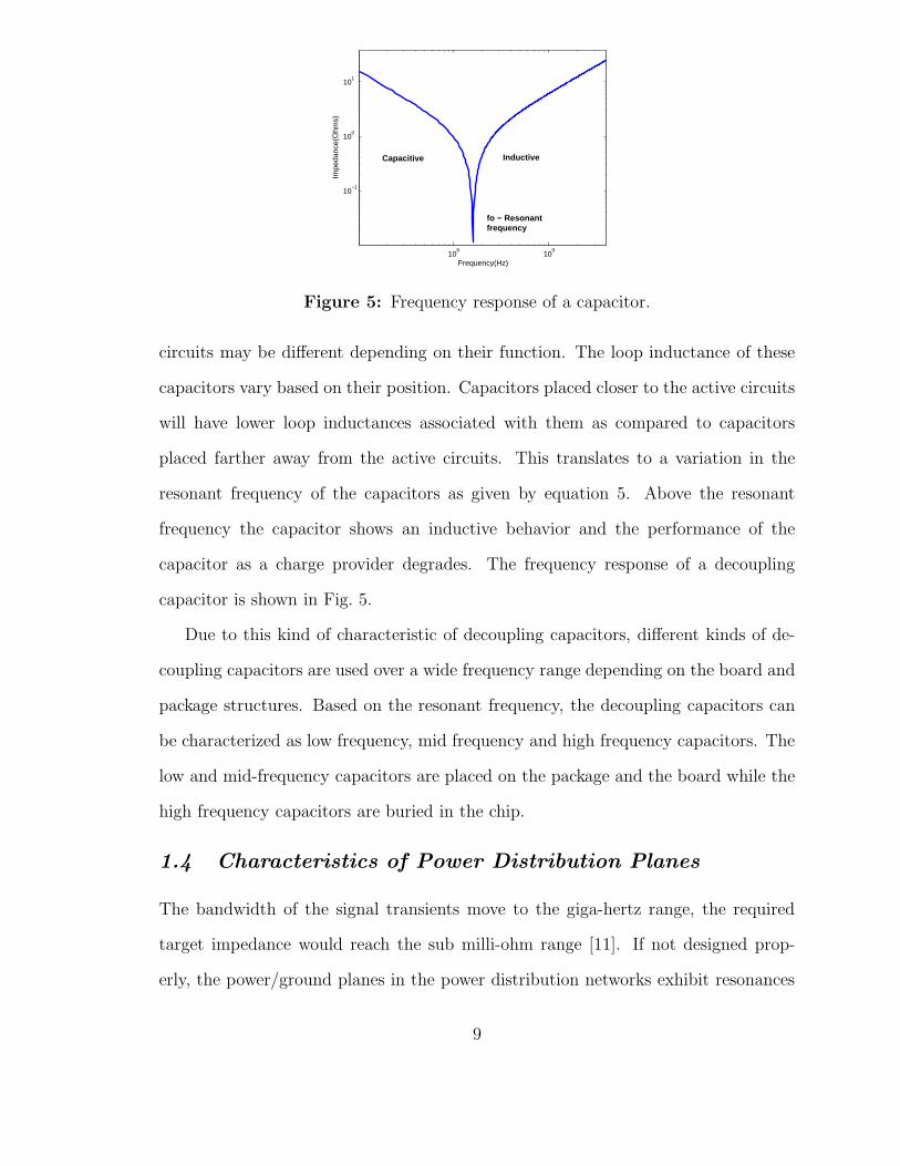
108
109
10−1
100
101
Frequency(Hz)
Impe
danc
e(O
hms)
Capacitive Inductive
fo − Resonantfrequency
Figure 5: Frequency response of a capacitor.
circuits may be different depending on their function. The loop inductance of these
capacitors vary based on their position. Capacitors placed closer to the active circuits
will have lower loop inductances associated with them as compared to capacitors
placed farther away from the active circuits. This translates to a variation in the
resonant frequency of the capacitors as given by equation 5. Above the resonant
frequency the capacitor shows an inductive behavior and the performance of the
capacitor as a charge provider degrades. The frequency response of a decoupling
capacitor is shown in Fig. 5.
Due to this kind of characteristic of decoupling capacitors, different kinds of de-
coupling capacitors are used over a wide frequency range depending on the board and
package structures. Based on the resonant frequency, the decoupling capacitors can
be characterized as low frequency, mid frequency and high frequency capacitors. The
low and mid-frequency capacitors are placed on the package and the board while the
high frequency capacitors are buried in the chip.
1.4 Characteristics of Power Distribution Planes
The bandwidth of the signal transients move to the giga-hertz range, the required
target impedance would reach the sub milli-ohm range [11]. If not designed prop-
erly, the power/ground planes in the power distribution networks exhibit resonances
9
in the frequency domain [12], and the resonances at certain frequencies may be higher
than the target impedance. In conventional designs decoupling capacitors are placed
in the PDN to suppress the resonances at the concerned frequencies. In addition, using
different materials and geometries of power-ground planes provide good suppression
of plane resonances in the PDN. For instance, an increase in the loss of a dielectric
material and a decrease in the dielectric thickness helps to reduce the impedance
and resonances [13],[14]. To examine the effects of power-ground planes in the PDN,
this section investigates the effect of dielectric loss, the dielectric constant, and the
dielectric thickness on the PDN.
1.4.1 Effect of Dielectric Loss
For low loss signal transmission , PCB materials with low dielectric loss have been
used; as a result, plane resonances are not suppressed sufficiently [13]. If the dielectric
material is to be used just between the power-ground plane then high loss dielectrics
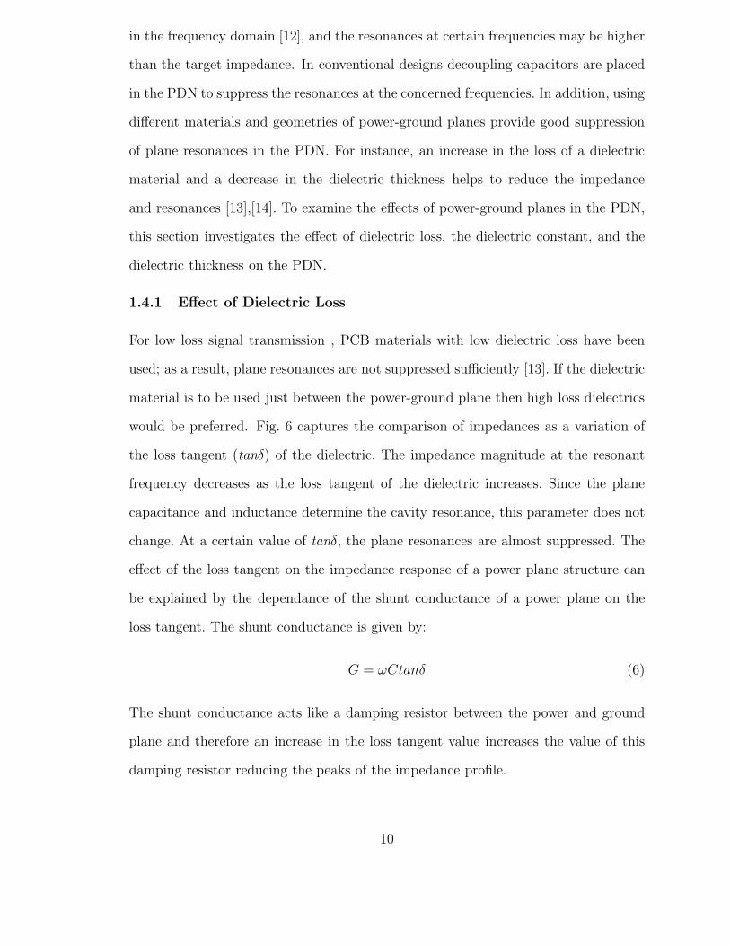
would be preferred. Fig. 6 captures the comparison of impedances as a variation of
the loss tangent (tanδ) of the dielectric. The impedance magnitude at the resonant
frequency decreases as the loss tangent of the dielectric increases. Since the plane
capacitance and inductance determine the cavity resonance, this parameter does not
change. At a certain value of tanδ, the plane resonances are almost suppressed. The
effect of the loss tangent on the impedance response of a power plane structure can
be explained by the dependance of the shunt conductance of a power plane on the
loss tangent. The shunt conductance is given by:
G = ωCtanδ (6)
The shunt conductance acts like a damping resistor between the power and ground
plane and therefore an increase in the loss tangent value increases the value of this
damping resistor reducing the peaks of the impedance profile.
10
Figure 6: Effect of dielectric loss on the plane impedance.
1.4.2 Effect of Dielectric Constant
Fig. 7, shows the effect of dielectric constant on the plane impedances and resonances
for dielectric constant (ǫr) = 4, 8, 16, 32 and 64 [14]. An increase in the plane
capacitance due to the increase in the dielectric constant reduces the low-frequency
impedance and the null and peak resonant frequencies shift to the lower frequen-
cies. This is because the velocity of the plane waves that propagate between the power
and ground plane varies inversely with√
ǫr. The increase in the delay of the plane
waves result in the downshift of the resonant frequency proportional to√
ǫr. The plane
impedances in the higher frequency range do not change much as it is determined by
the inductance of the power/ground plane, which is fixed.
1.4.3 Effect of Dielectric Thickness
Thin dielectrics between power/ground planes offer advantages in the low as well as
high frequency range. For the analysis in this section assume a unit cell of the power
plane of length and width w. The capacitance of the unit cell of the power plane is
11

Figure 7: Effect of dielectric constant on the plane impedance.
given by equation 7
C =ǫoǫrw
2
d(7)
Where ǫo, ǫr are the permittivity of free space and relative dielectric constant of the
material. A is the area of the power plane and d is the separation between the power
and ground plane. The inductance of the unit cell of the power ground plane is given
by the equation
L = µod (8)
µo is the permeability of free space. From, the above equations it is evident that
the thinner dielectrics increase the capacitance of the planes and reduce the plane
inductance. Thinner dielectrics reduce the impedance over the frequency range as
well. This can be explained by the relationship of the impedance of the power-ground
plane with the capacitance and the inductance, given by equation 9:
Z = sqrt(L
C) (9)
An increase in the capacitance and decrease in the inductance reduces the impedance
of the power planes. The velocity of a wave between the power-ground plane is given
12

Figure 8: Effect of dielectric thickness on the plane impedance.
by equation 10
v =1
sqrt(LC)(10)
From the above equation it can be inferred that the peak and null resonant frequencies
do not change since the velocity of the wave remains constant since it is not a function
of dielectric thickness. The effect of dielectric thickness on the plane impedance is
shown in Fig. 8 [13].
1.5 Decoupling Methodologies used in today’s systems
The different decoupling methodologies used in today’s PDNs will be highlighted in
this section. The methodologies are listed below:
a)”Multi-pole” (MP) [3]
b)”Big-V” [15]
c)”Distributed Matched Bypassing” (DMB) [16]
d)”Extended Adaptive Voltage Positioning” (EAVP)
In terms of the impedance profile, the first three methodologies are very similar
13
to each other. There is no clear boundary between these design approaches and one
method can be transformed into another by varying certain parameters. The DMB
methodology, calls for a flat impedance profile from DC to a certain corner frequency
after which the impedance can increase linearly based on the inductance value. In
this methodology, elements with Q < 1 are used. The Q < 1 condition creates a
shallow flat bottom on the impedance curve of each capacitor bank. Capacitor banks
that are adjacent on the frequency axis can be represented by a lower frequency R-L
and higher frequency R-C elements in parallel. This network approximation is valid
only in the vicinity of the capacitor banks as it neglects the capacitance of the lower
bank and the inductance of the higher bank. As long as the serial losses between the
elements of the DMB network are not significant, the PDN can be represented by
a number of such cells in parallel. In the MP design methodology, different values
of capacitors are chosen to cover the frequency band over which decoupling has to
be provided. The impedance profile of the resultant design of the PDN has multiple
peaks and the choice of the capacitors to decouple higher frequency bands depends
on the inductance of the capacitor used to decouple the lower frequency region. In
the ”Big-V” method, a number of capacitors of the same type and value are used to
create a ”V” in the impedance profile response. The value of the ”V” being far below
the target impedance. The comparison of the resultant impedance profile of the three
methodologies is shown in Fig. 9 [17].
The EAVP method is based on the theory of adaptive voltage positioning (AVP),
which is commonly used in voltage regulator module (VRM) design and opera-
tion [18]. The (AVP) design will be briefly discussed in this part of the section. The
circuit used in AVP is shown in Fig. 10 [19]. The voltage is set to VCC + TOL when
no current is consumed as shown in Fig. 11 [19]. When all the current is consumed,
the voltage is then VCC − TOL. Initially, all the ICC current is supplied by the bulk
capacitor, thereby setting the initial voltage drop to ICCMAX ×RBLK . In the steady
14
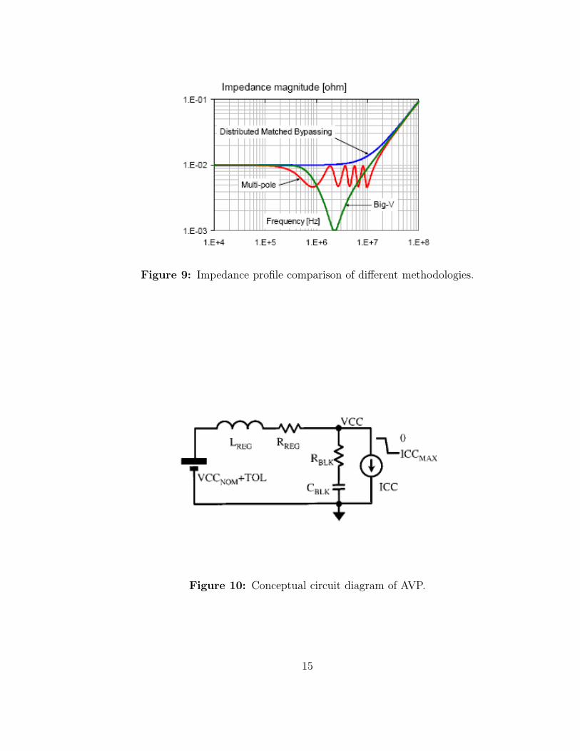
Figure 9: Impedance profile comparison of different methodologies.
Figure 10: Conceptual circuit diagram of AVP.
15

Figure 11: Adaptive voltage positioning waves.
state the voltage drop is ICCMAX×RREG. For identical voltage droops at t = 0 and in
the steady state, RBLK = RREG should be enforced. Also, to achieve zero overshoot
and undershoot, the inductive and capacitive time constants has to be met.
RBLK .CBLK =LREG
RREG(11)
To meet the tolerance window, RBLK has to be given by:
RBLK =V cc × 2 × TOL
ICCMAX(12)
Since the effectiveness of the bulk capacitors at higher frequencies is limited by its
parasitic inductance LBLK , the EAVP method was introduced. EAVP extends the
method that was used for optimized AVP design of bulk capacitors to the successive
designs of the mid-frequency and die capacitance parameters. The basic rules used
in this methodology are as follows:[19]
Rule 1) Select the equivalent series resistance of the decoupling stage N to be equal
to the effective series R of the decoupling stage N − 1.
Rule 2) Select the RC time constant of the decoupling stage N to match the L/R
time constant of stage N − 1 or select the Z(f) 3DB point of decoupling stage N to
the Z(f) +3DB point of stage N − 1.
16
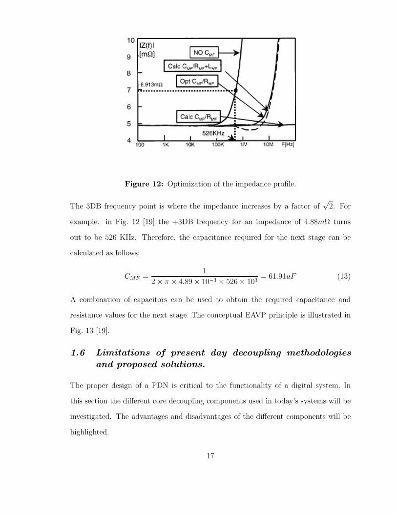
Figure 12: Optimization of the impedance profile.
The 3DB frequency point is where the impedance increases by a factor of√
2. For
example. in Fig. 12 [19] the +3DB frequency for an impedance of 4.88mΩ turns
out to be 526 KHz. Therefore, the capacitance required for the next stage can be
calculated as follows:
CMF =1
2 × π × 4.89 × 10−3 × 526 × 103= 61.91uF (13)
A combination of capacitors can be used to obtain the required capacitance and
resistance values for the next stage. The conceptual EAVP principle is illustrated in
Fig. 13 [19].
1.6 Limitations of present day decoupling methodologiesand proposed solutions.
The proper design of a PDN is critical to the functionality of a digital system. In
this section the different core decoupling components used in today’s systems will be
investigated. The advantages and disadvantages of the different components will be
highlighted.
17
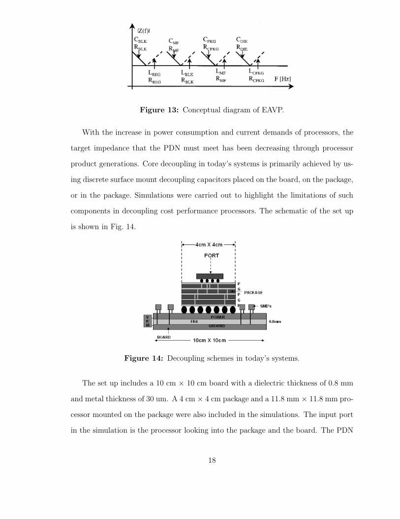
Figure 13: Conceptual diagram of EAVP.
With the increase in power consumption and current demands of processors, the
target impedance that the PDN must meet has been decreasing through processor
product generations. Core decoupling in today’s systems is primarily achieved by us-
ing discrete surface mount decoupling capacitors placed on the board, on the package,
or in the package. Simulations were carried out to highlight the limitations of such
components in decoupling cost performance processors. The schematic of the set up
is shown in Fig. 14.
Figure 14: Decoupling schemes in today’s systems.
The set up includes a 10 cm × 10 cm board with a dielectric thickness of 0.8 mm
and metal thickness of 30 um. A 4 cm × 4 cm package and a 11.8 mm × 11.8 mm pro-
cessor mounted on the package were also included in the simulations. The input port
in the simulation is the processor looking into the package and the board. The PDN
18
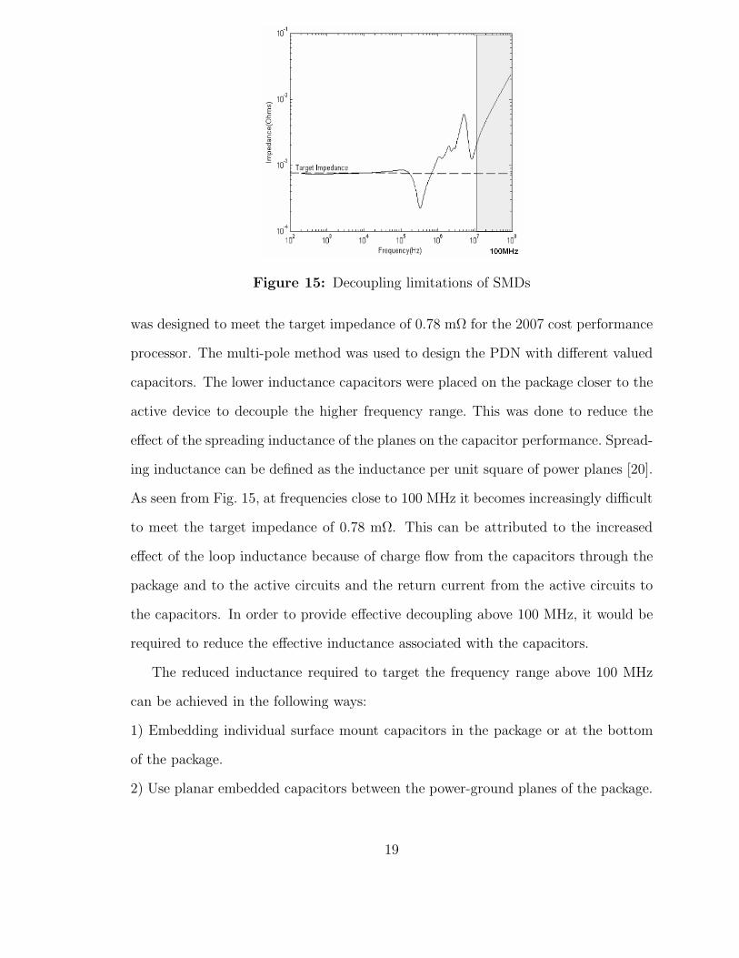
Figure 15: Decoupling limitations of SMDs
was designed to meet the target impedance of 0.78 mΩ for the 2007 cost performance
processor. The multi-pole method was used to design the PDN with different valued
capacitors. The lower inductance capacitors were placed on the package closer to the
active device to decouple the higher frequency range. This was done to reduce the
effect of the spreading inductance of the planes on the capacitor performance. Spread-
ing inductance can be defined as the inductance per unit square of power planes [20].
As seen from Fig. 15, at frequencies close to 100 MHz it becomes increasingly difficult
to meet the target impedance of 0.78 mΩ. This can be attributed to the increased
effect of the loop inductance because of charge flow from the capacitors through the
package and to the active circuits and the return current from the active circuits to
the capacitors. In order to provide effective decoupling above 100 MHz, it would be
required to reduce the effective inductance associated with the capacitors.
The reduced inductance required to target the frequency range above 100 MHz
can be achieved in the following ways:
1) Embedding individual surface mount capacitors in the package or at the bottom
of the package.
2) Use planar embedded capacitors between the power-ground planes of the package.
19
3) Use thin/thick film embedded discrete capacitors within the package.
4) Use on-chip capacitance to decouple the higher frequency bands.
The above core decoupling strategies were investigated to highlight their effectiveness
in decoupling above 100 MHz.Traditionally, discrete decoupling capacitors placed on
the surface of the board or the package have been used to decouple active switching cir-
cuits [3],[21],[22],[23]. However, with an increase in the clock rates and its harmonics
with technology nodes [2], decoupling has to be provided in the GHz range. Discrete
surface mount capacitors can be attached to the bottom of the package as shown in
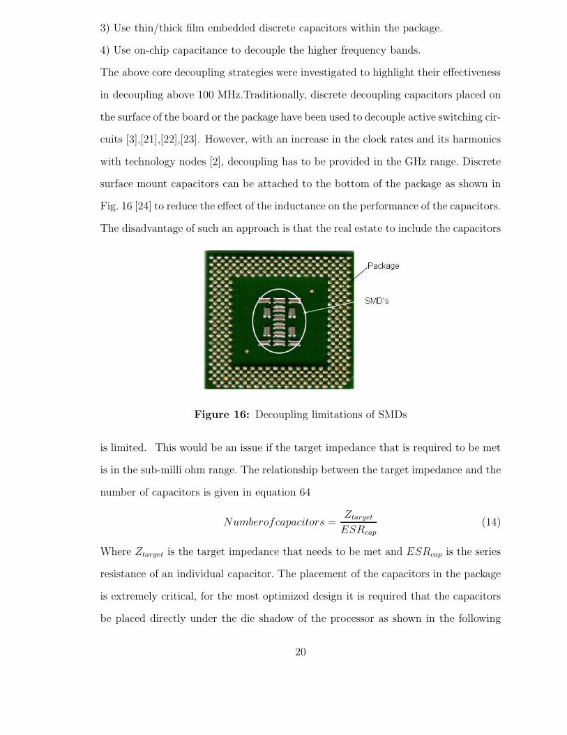
Fig. 16 [24] to reduce the effect of the inductance on the performance of the capacitors.
The disadvantage of such an approach is that the real estate to include the capacitors
Figure 16: Decoupling limitations of SMDs
is limited. This would be an issue if the target impedance that is required to be met
is in the sub-milli ohm range. The relationship between the target impedance and the
number of capacitors is given in equation 64
Numberofcapacitors =Ztarget
ESRcap(14)
Where Ztarget is the target impedance that needs to be met and ESRcap is the series
resistance of an individual capacitor. The placement of the capacitors in the package
is extremely critical, for the most optimized design it is required that the capacitors
be placed directly under the die shadow of the processor as shown in the following
20

Figure 17: Sensitivity of capacitor performance with position.
analysis. Capacitors were placed on a 10 cm × 10 cm power plane. The capacitor per-
formance is sensitive to position as shown in Fig. 17. The solid line is the performance
of the capacitor at the probe location, while the dashed line is the capacitor perfor-
mance placed 10 mm away from the probe point. The degradation of the frequency
response of the capacitors with location is clearly evident and is because of the effect
of the inductance and resistance of the power planes. Therefore, the desired frequency
may not be targeted because of the plane parasitics. An important requirement of
these capacitors is to be able to place them as close to the switching circuits as pos-
sible. In the case of discrete embedded capacitors the most important criteria would
be to place them directly under the die shadow. Another option would be to use
embedded planar capacitors in the PDN. This option has been investigated as shown
in [25],[26],[27],[28],[29]. The planar capacitor is primarily a layer of thin dielectric
between the power and ground plane in the board or the package. The performance
of an embedded planar capacitor layer in a package was investigated. The embedded
planar capacitor is connected to the active device with thru vias that extend from the
21
107
108
109
1010
10−4
10−3
10−2
10−1
100
101
102
frequency (Hz)
Zin
mag
nitu
de
110ports
64ports
32ports
16ports
8ports
4ports
3ports
2ports
1port
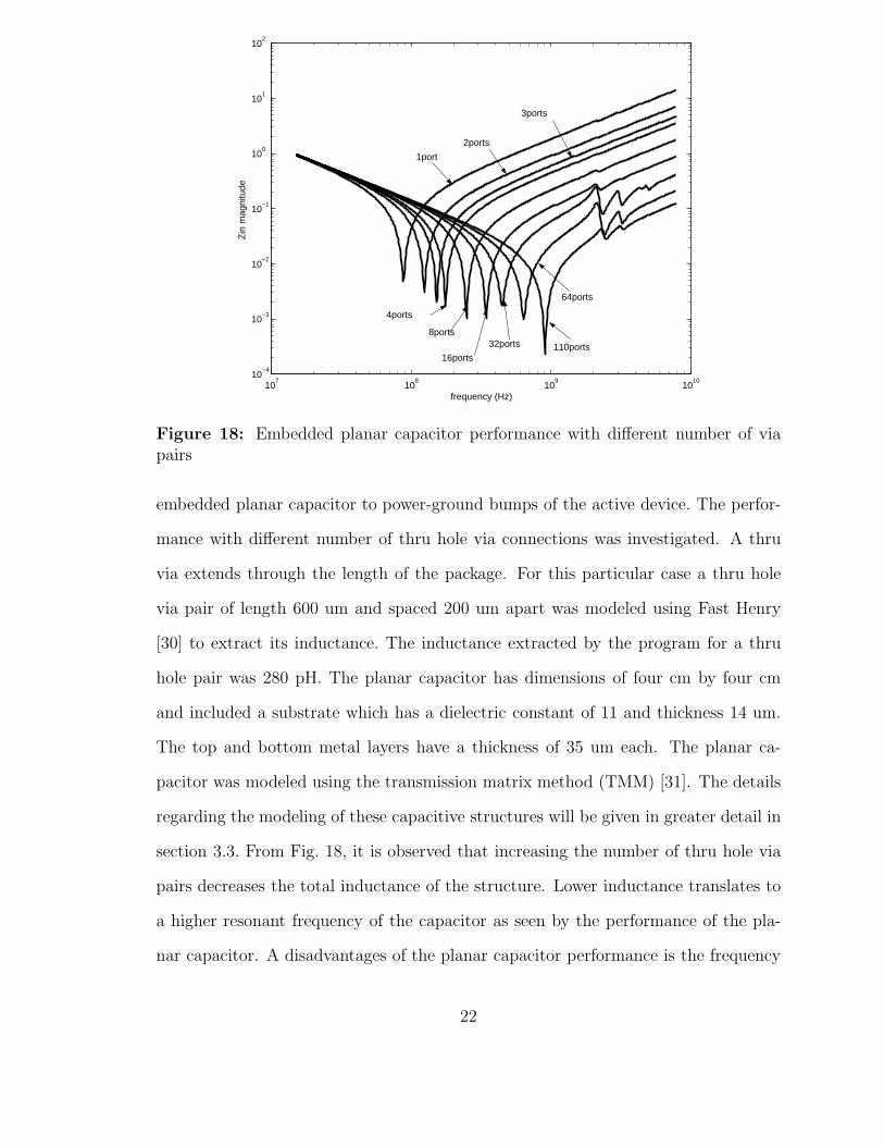
Figure 18: Embedded planar capacitor performance with different number of viapairs
embedded planar capacitor to power-ground bumps of the active device. The perfor-
mance with different number of thru hole via connections was investigated. A thru
via extends through the length of the package. For this particular case a thru hole
via pair of length 600 um and spaced 200 um apart was modeled using Fast Henry
[30] to extract its inductance. The inductance extracted by the program for a thru
hole pair was 280 pH. The planar capacitor has dimensions of four cm by four cm
and included a substrate which has a dielectric constant of 11 and thickness 14 um.
The top and bottom metal layers have a thickness of 35 um each. The planar ca-
pacitor was modeled using the transmission matrix method (TMM) [31]. The details
regarding the modeling of these capacitive structures will be given in greater detail in
section 3.3. From Fig. 18, it is observed that increasing the number of thru hole via
pairs decreases the total inductance of the structure. Lower inductance translates to
a higher resonant frequency of the capacitor as seen by the performance of the pla-
nar capacitor. A disadvantages of the planar capacitor performance is the frequency
22
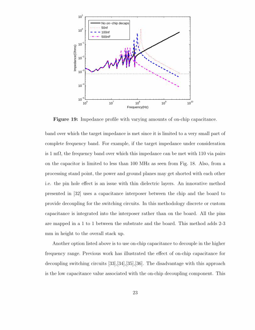
106
107
108
109
1010
10−5
10−4
10−3
10−2
10−1
100
101
Frequency(Hz)
Impe
danc
e(O
hms)
No on−chip decaps50nf100nf500nF
Figure 19: Impedance profile with varying amounts of on-chip capacitance.
band over which the target impedance is met since it is limited to a very small part of
complete frequency band. For example, if the target impedance under consideration
is 1 mΩ, the frequency band over which this impedance can be met with 110 via pairs
on the capacitor is limited to less than 100 MHz as seen from Fig. 18. Also, from a
processing stand point, the power and ground planes may get shorted with each other
i.e. the pin hole effect is an issue with thin dielectric layers. An innovative method
presented in [32] uses a capacitance interposer between the chip and the board to
provide decoupling for the switching circuits. In this methodology discrete or custom
capacitance is integrated into the interposer rather than on the board. All the pins
are mapped in a 1 to 1 between the substrate and the board. This method adds 2-3
mm in height to the overall stack up.
Another option listed above is to use on-chip capacitance to decouple in the higher
frequency range. Previous work has illustrated the effect of on-chip capacitance for
decoupling switching circuits [33],[34],[35],[36]. The disadvantage with this approach
is the low capacitance value associated with the on-chip decoupling component. This
23
renders them effective at frequencies beyond one to two GHz. The amount of on-chip
capacitance can be increased, but this would compromise the amount of real estate
available for including logic circuits.
To overcome the limitations of the SMDs, planar embedded capacitors, and on-
chip capacitance the proposed solution is to use discrete thin/thick film capacitors
that can be used within the package as shown in Fig. 28. These capacitors can be
designed with variable sizes, have different capacitances, and therefore resonate at
different frequencies. The proximity of these capacitors to the active devices reduces
the loop inductance as compared to the SMDs and are effective in targeting frequen-
cies above 100 MHz. Another advantage of using individual thick film capacitors is
the high value of capacitance that can be obtained by using this technology.
SSN can be produced by improper return current path as shown in [4]. I/O de-
coupling is achieved by providing a low impedance path to the return current for the
I/O signals. This can be achieved by using embedded planar capacitors in the board.
The thin dielectrics increase the capacitance and reduce the inductance decreasing
the overall impedance of the structure, therefore providing low impedance for the re-
turn current and reducing the noise produced. The details regarding the performance
improvements will be explained in detail in chapter 5 of this thesis.
1.7 Proposed Research and Dissertation Outline
The objective of the proposed research is to highlight the performance benefits of
using embedded thin/thick film capacitors in decoupling active and I/O circuits. The
case for embedded capacitors is made for future packages and boards supporting
multi-core processors. This includes investigating the limitations of SMDs in decou-
pling over 100 MHz to maintain target impedances in the order of milli-ohms. The
design, modeling, and measurement of embedded capacitors is done in this thesis.
24

The design of an array of embedded package capacitors to decouple the mid-band fre-
quency from 100 MHz to 2 GHz and the performance benefits of using this embedded
capacitor array is highlighted in the time and frequency domain. This research also
includes the use of embedded planar capacitors in boards to decouple I/O circuits.
The simultaneous switching of active circuits leads to generation of noise in the
PDN that can propagate and degrade the performance of logic blocks in the vicinity.
Therefore, the mitigation of this noise is critical for the proper functionality of a dig-
ital system. Based on the issues of noise generation and performance degradation in
digital systems, the following research is proposed:
1) Power dissipation of processors: High power processors put stringent re-
quirements on the design of PDNs, since higher power translates to a lower target
impedance that must be met by the PDN. Therefore, an investigation of the different
power dissipation components of processors and a methodology to improve overall
performance of processors by reducing the power dissipation and increasing the off-
chip bandwidth was done in this thesis. The work done regarding processor power
dissipation is listed below:
a) The different components of power dissipation of a processor were investigated.
This primarily included the active, static, and I/O power dissipation components.
b) The active power dissipation through the technology nodes was calculated by us-
ing an active power dissipation calculation tool SUSPENS [37] and the static power
was calculated based on the numbers from ITRS. The numbers obtained from this
analysis compared well with the existing numbers of processor power dissipation.
c) The trend of processor power dissipation through technology nodes predict that
these numbers would far exceed the maximum amount of power that a package can
sustain as per ITRS. Therefore, an analysis into the methodology of reducing power
25
dissipation while increasing the performance was done. Off-chip bandwidth was de-
fined as performance parameter. This methodology involves the use of multi-core pro-
cessors to achieve the required performance numbers while reducing the overall power
dissipation. The packaging platform required to sustain such high off-chip bandwidth
is investigated in the thesis.
2) Individual Thin/Thick Film Embedded Package Capacitors: The limita-
tion of SMDs in decoupling active circuits is done with the aid of a PDN modeling
tool. The analysis was done to investigate the performance of the SMDs to decouple a
PDN with a target impedance in the order of milli-ohms and the advantages of using
embedded package capacitors in such scenarios is highlighted. This work included the
following:
a) The limitations of SMDs by modeling a PDN with SMD type decoupling capacitors
to decouple a high-end microprocessor is shown. The limitations of embedded planar
capacitors to meet similar decoupling requirements are also highlighted in this thesis.
The different technologies that enable embedded package capacitors are highlighted.
b) The measurement of the embedded capacitors using a two port frequency domain
measurement technique is done. The repeatability and robustness of this technique
is highlighted by carrying out a series of similar measurements and comparing the re-
sults. The frequency dependent capacitance, inductance, and resistance is extracted
over the measured frequency range.
c) The capacitive structures are modeled and the model to hardware correlation for
the different structures are shown by compensating for the excess inductance of the
probes.
d) Using the models developed for the capacitor structures, an array of embedded ca-
pacitors within the package was designed to decouple the mid-band frequency range
26

from 100 MHz to 2 GHz using different sized capacitors. Different arrays were de-
signed with the capacitor technologies developed at the Packaging Research Cen-
ter (PRC) and by DuPont technologies respectively. The performance investigation
in the time and frequency domain were done for both arrays and a significant im-
provement was observed for both cases.
e) An analysis into the SMD saving with the use of embedded capacitors within the
package is also highlighted in this thesis.
f) The benefits of core and I/O decoupling using embedded capacitors was done by
implementing the concept on an actual ten metal layer package developed at IBM.
The benefits in on-chip capacitance savings using embedded package capacitors is
highlighted.
3) Embedded Planar Capacitors: The performance of embedded planar capaci-
tors to decouple I/O circuits and improving the overall impedance profile is shown.
This work involved the following:
a) Characterization of the impedance profile of a stack up with different thicknesses
of planar capacitors was done. The difference in the thickness of the dielectrics trans-
lates into a difference in the impedance profile, which is captured using the two port
frequency domain measurements.
b) The noise coupling suppression between the signal lines and the power-ground
plane was developed. A variation in the noise isolation was observed for the different
dielectric thicknesses.
c) Models were developed for the different stripline configurations in the stack-up
using modal decomposition and were coupled with the power-ground models to get
model to hardware correlation between the model and the measurements.
d) An active test vehicle with the different embedded capacitor dielectric thickness
was designed with a 100 MHz clock generator as the source to compare the I/O de-
coupling performance. Model to hardware correlation between the measurements and
27

the model were obtained and have been included in the thesis.
e) Simulations were carried out for single ended and differential lines at 1 Gbps and
5 Gbps with different dielectrics, the difference in the performance was captured by
the SSN and eye diagram results.
The remainder of the thesis is organized as follows. Chapter 2 presents power dis-
sipation investigation of processors and a proposed methodology to improve overall
performance by reducing the power dissipation and increasing the total off-chip band-
width of processors. The case for embedded capacitors in the package and the board
are made in this chapter. Chapter3 investigates the measurement, modeling, and
characterization of the embedded capacitors with results showing the model to mea-
surement correlation. Chapter4 deals with the implementation of these capacitors
in the design of a capacitor array to decouple core circuits of processors. The per-
formance of embedded planar capacitors in improvement of impedance profile, noise
suppression, and decoupling I/O circuits by offering low impedance return current
paths is highlighted in chapter 5. The conclusion and future work are presented in
chapter 6.
28
CHAPTER II
PACKAGE REQUIREMENTS FOR MULTI-CORE
PROCESSORS
The increasing power trends of processors is putting stringent requirements on the
design of PDNs. This is evident with the decreasing target impedances that must
be met through the successive technology nodes [table 1]. Therefore an analysis into
the different power dissipation components and the use a multi-core processor ap-
proach to improve the performance of a processor is investigated. An analysis of the
performance trade-offs between single and multi-core processors based on power, fre-
quency, bandwidth, and the role of embedded passives with high density wiring in
future packages to support such processors is investigated.
Power in a microprocessor relates to both consumption and dissipation. To main-
tain the performance improvements of microprocessors, a solution to the power dis-
sipation problem must be found. This would require good power dissipation designs
and thermal management solutions. Microprocessor power densities have grown over
the technology nodes due to the increase in the number of transistors (active capaci-
tance) and increase in the processor frequency. The supply voltage has scaled down
by a factor of 0.8 instead of 0.7 per technology node. The major contributors to the
power dissipation of microprocessors in the sub 100 nm node are the active power and
leakage power dissipation components. The leakage power scales by a factor of about
five in each technology node while the active power scales by a factor of one. Another
major challenge for future microprocessors is the performance of on-chip wires at
higher processor operating frequencies. Global interconnections on the integrated cir-
cuit (IC) that span at least half a chip edge are major causes of latency because of RC
29

and transmission line delay. While the transistor gate delay decreases linearly with a
decrease in the minimum feature size, the wire delay stays nearly constant or increases
as the wires become finer and longer. This is due to the increasing wire resistance to
load capacitance ratios. In addition, processor clock rates have been increasing and a
long wire can affect the processor’s cycle time if it belongs to a critical timing path.
The result of the above trends is that the micro-architecture of future processors will
be critical to the processor performance. The processor resources that communicate
with each other in a single cycle must be physically close to each other. This type of
architecture would require a CPU consisting of higher speed logic blocks connected
by shorter wires.
With the above-mentioned concerns and architectural challenges, the Chip mul-
tiprocessor architecture (CMP) has been shown to have the best performance of all
the proposed architectures. In the CMP architecture the die is divided into a group
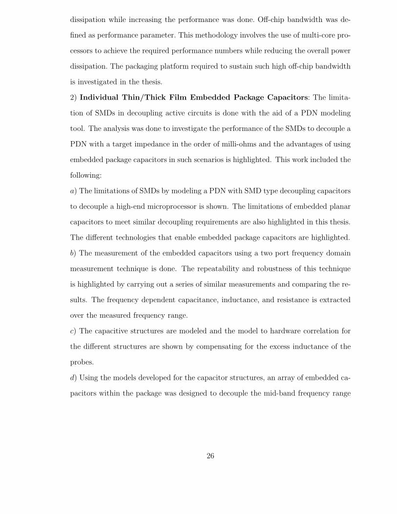
of small identical processing cores, that work in parallel with each other [38]. Fig. 20
shows an example of a SPARC microprocessor that is made of eight cores with a
shared cache [39]. In this chapter we propose to use the multi-core processor ap-
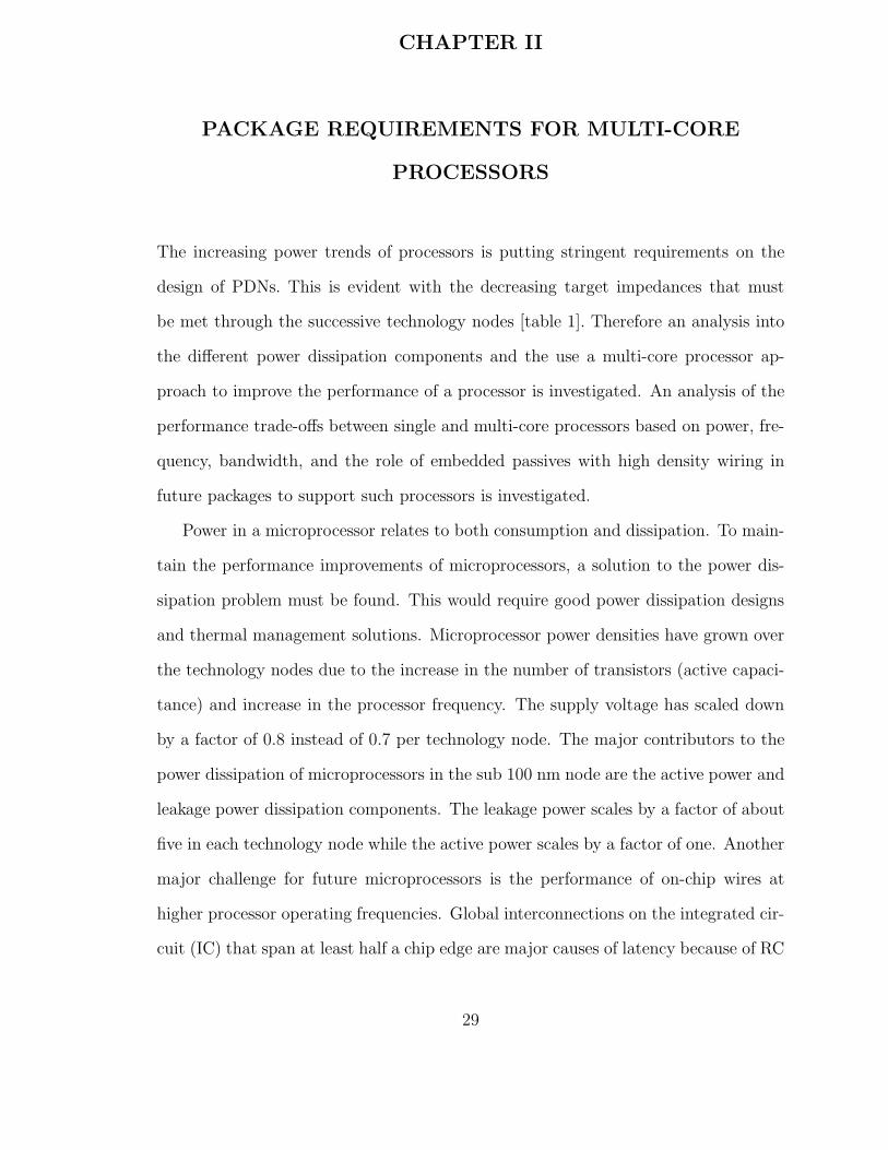
proach to improve the performance of a processor. The performance parameters are
defined as the power dissipation and the total bandwidth of the processor. It has
been shown that by using a scalable architecture a multi-core processor can outper-
form the next generation single-core processor [40], [41]. Using the scalable approach
an improvement in the bandwidth of a processor can be achieved. Fig. 21, shows the
performance improvement expected from using multi-core processors as compared to
a single-core processor [42].
The power dissipation for future cost performance processors is expected to be
close to 450 W by the end of the decade. Such high value of power dissipation
would not be acceptable for single chip package solutions. Leakage power is a major
contributor to the total power dissipation and constitutes close to 50% of the total
30
Figure 20: SPARC multi-core processor.
Figure 21: Expected relative performance improvement of a multi-core processorover a single-core processor.
31
power dissipation for future technology nodes. Therefore, to improve the total power
dissipation of the processor, both the active and the leakage power will have to be
reduced. A reduction in the power dissipation and an increase in the total bandwidth
are achievable using the multi-core approach. This chapter discusses an analysis on
the architectural trade-offs between single and multiple processors based on power,
frequency, and performance. The multi-core approach would need an extremely high
number of I/Os and interconnects to support bandwidths of the order of 1 TByte/s for
communications between ICs. The packaging technologies that can enable multi-core
processors will be highlighted. An analysis on the need for fine lines and microvias in
the package along with fine pitch interconnections between the chip and the substrate
is discussed. Embedded passives and microvias are enabling technologies that can
provide the maximum amount of functionality and the best electrical performance
in the package. All the above technologies can be realized with the system on a
package (SOP) paradigm and are required for multi-core processors in the future.
This chapter is organized as follows: Section 2.1 discusses the theory behind the
power dissipation in active circuits. Section 2.2 explains the methodology used in
the power dissipation calculations of the processor for different technology nodes. In
Section 2.3 an analysis of the advantages of the multi-core approach is discussed.
2.1 Processor Power Dissipation Calculations
Power dissipation of processors is increasing at an alarming rate through the technol-
ogy nodes as shown in Fig 22. Active and static power are the main contributors to
the total power dissipation in a processor. The general equation that describes active
power dissipation is as follows:
Pactive = aCV 2f (15)
32

Figure 22: Power dissipation, frequency of operation and bandwidth variation ofsingle-core processors through technology nodes.
Here a is the activation factor of the processor. This number varies between 7%
to 15% depending on the application. C is the total switching capacitance of the
processor. In equation (15), the frequency of operation of the processor is f and V
is the supply voltage. The power lost due to the momentary short circuit at a gates
output is given as follows:
Pshort = taIshortV (16)
Here t is the time for which the short circuit current Ishort flows. This term has
been ignored since the power loss is very small and it contributes to the active power
dissipation. The static power dissipation of a processor is given by:
Pstatic = V Ileakage (17)
Where Ileakage is the total leakage current in the processor. The third contributor to
the total power dissipation is the I/O power or the off chip driving power dissipation.
The I/O power is given by:
33
Pi/o = 0.5CV 2f (18)
Where C is the capacitance that the off chip driver has to charge and discharge. It is
the sum of the output capacitance of the driver, the on-chip interconnect capacitance,
the solder ball capacitance, and the capacitance of the interconnect on the carrier.
Therefore, the total power dissipation of the processor Ptot is given by:
Ptot = Pactive + Pstatic + Pi/o (19)
The power trends shown in Fig. 22 far exceed the power dissipation numbers given
in the International Roadmap for Semiconductors (ITRS) [2]. Therefore, in order to
meet the ITRS numbers it would be required to decrease the total power dissipation
of the processor. This can be achieved if the active and static power dissipation
components can be reduced. The analysis used to obtain the numbers in Fig. 22 is
explained in section 2.2 of this chapter. The leakage current in a transistor which is
the source of the static power dissipation is a combination of the subthreshold and
gate oxide leakage.
Ileakage = Isub + Igoxide (20)
The subthreshold leakage current is given as [43]:
Isub = K1 ∗ W ∗ e−Vthq
nkT (1 − e−V q
nkT ) (21)
The term kT/q is the thermal voltage and is 25 mV at room temperature. W is the
width of the gate of a transistor. For calculating the total subthreshold leakage, the
combined gate widths of all the transistors in the processor is taken as a measure of
W . The terms K and n are experimentally derived and are technology dependent.
The gate oxide leakage occurs because of tunnelling of charge carriers through the
34
gate due to the presence of a high electric field. The gate oxide leakage current is
given in a simplified form as follows [43]:
Igoxide = K2 ∗ W ∗ V
Toxe
−βToxV (22)
where K2 and β are experimentally derived parameters. Tox is the thickness of the
gate oxide and from equation (22) it is observed that an increase in the thickness of
the gate oxide would reduce the gate oxide current. This would be against the scaling
trends since Tox must decrease proportionally with the technology nodes. Therefore,
another option is to increase the dielectric constant of the gate oxide.
However, the major contributor to the leakage power is the subthreshold leakage
component [2]. Therefore, Isub would need to reduce to decrease the static power
dissipation. From equation (21) there are two ways of reducing Isub. The first one
involves switching off the supply voltage, which would make Isub = 0. The second
approach would be to increase the threshold voltage Vth. Increasing Vth will reduce
Isub because of the negative exponential dependence relation between the two terms.
The supply voltage V is also a variable in the static power reduction scenario since
it is expected to scale from 1.2 V at the 90 nm technology node to 1 V at the 45 nm
technology node for high performance logic. The next part of this section explores
the relation between the frequency of operation of the transistor, the supply voltage,
and the threshold voltage. The gate delay (Tg) of the chip can be modeled as that of
an inverter using the alpha-power model [44]:
Tg αV
V − Vthγ (23)
Therefore, the frequency of operation of the chip can be given by
f α1
Tg ∗ Ld
αV − Vth
γ
V Ld
(24)
35
In equation (24), Ld is the logic depth of the processor. From equation (24) it is
observed that an increase in the threshold voltage Vth will reduce the frequency of
operation if the supply voltage V is kept constant. To compensate for the reduction in
the processing resulting from the loss in the frequency of the processor, the scheduled
task can be processed in parallel at a reduced operating frequency.
2.2 Power Dissipation Calculations
Equations (15) through (24) in the previous section deals with the general relationship
between the voltages, currents, frequency of operation and the active as well as static
power dissipation components. In this section a quantitative look into how these
factors affect the total power dissipation through the technology nodes is discussed.
The active power component given in equation (15) depends on the total capac-
itance that has to be switched by the driver. This capacitance includes the output
capacitance of the driver, the capacitance of the interconnect on which the signal
propagates, and the input capacitance of the receiver circuit. The analysis carried
out in this thesis assumes a basic logic block as shown in Fig. 23.
Fig. 23 shows a three input/output NAND gate, which is connected to another
three input NAND gate by an interconnect. The method used to calculate the total
active power dissipation was based on SUSPENS [37], a system level circuit model
for CPUs. The input parameters for all the variables were taken from the ITRS
roadmap. This power model was used to calculate the active power dissipation upto
the 45 nm node by varying the input parameters based on the technology node. The
static power dissipation was calculated by taking the static power dissipation per unit
length value from the ITRS and multiplying that by the average gate width of all the
transistors in the microprocessor. A few of the parameters used in calculating the
active power dissipation numbers, that were input to SUSPENS are listed in table 2.
The width of an N type metal oxide semiconductor (NMOS) and P type metal
36

Table 2: Input parameters to calculate active power dissipation in SUSPENS forthe 90 nm technology node
Input gate capacitance 7.392×10⁻¹⁶ FInput capacitance for a min-imum sized NMOS
3.256×10⁻¹⁷ F
Interconnect Capacitance 7.36×10⁻¹⁶ FTotal capacitance of the in-terconnect per unit length
8.2×10⁻¹¹ F/m
Permittivity of free space 8.854×10⁻¹² F/mPermeability of free space 1.257×10⁻⁶ H/mChip side length 11.8 mmInterconnet pitch(Assumedequal on all layers)
5.1×10⁻⁷ m
Chip clock frequency 3.2 GHzRent exponent within a chip 0.404Width to length ratio of thetransistors in a logic gate
11.34
Relative permittivity of ox-ide
3
Switching factor of all gates 0.15Average fan out of logicgates
3
Number of wiring layers 13Number of logic gates on achip
32166667
Logic depth 25Core voltage supply 1.2 V
37

Figure 23: Basic logic gate used in the analysis.
oxide semiconductor (PMOS) are defined as follows:
NMOSwidth = ASICHalfpitch × 4 (25)
PMOSwidth = NMOSwidth × 2 (26)
For the 90 nm technology node the ASIC half pitch length is 90 nm. Therefore, the
NMOS and PMOS widths are 360 nm and 720 nm respectively. The average width
to length ratios is assumed to be 15, which is a standard assumption for logic gates.
The physical gate length of a processor in the 90 nm technology node is 37 nm [2].
The static power dissipation per transistor gate length in the 90 nm technology node
is 6.6× 10⁻¹⁶ W/um [2]. The results of the above approach for the 90 nm technology
node are as follows: The active power = 77 W and the static power = 70.69 W.
Comparing these values to the intel power trends [45], the active and static power are
approximately 80 W and 65 W respectively. The power dissipation values obtained
at higher technology nodes also compare with the projections [41]. Therefore, the
general power dissipation trends are captured using this method and has been used
38

to carry out further analysis. The I/O power is calculated using equation (18), the
capacitance variable in the equation is the sum of the on-chip, solder ball, and off-chip
interconnect capacitance. The on-chip interconnect capacitance is calculated using
the formula in [46].
C1
ǫox= 2.80(
T
H)0.222 + 1.15
W
H(27)
Where T and W are the thickness and width of copper respectively. H is the height
of copper above the ground plane. For the 90 nm technology node the average capac-
itance of the on-chip interconnect is 8.2 × 10⁻¹¹ F.
In Table 3, the power dissipation, operating frequency ,chip-package data rate,
and bandwidth are shown through the technology nodes. The off-chip bandwidth
(amount of data) of a processor is defined as the product of the off-chip bus speed
and the number of I/Os that carry these high speed signals.
off chip bandwidth = off −chip bus speed× number of high−speed I/Os (28)
For reducing the total power dissipation of the processors it would be required to
reduce the active and static power dissipation. The static power dissipation can be
reduced by reducing the subthreshold current as seen in equation (21). The method
for reducing the subthreshold current is by increasing the threshold voltage (Vth). An
increase in Vth reduces the frequency of operation as shown in equation (24). This re-
duction in frequency will also reduce the active power dissipation from equation (15).
This approach however would lead to a decrease in the performance of the processor,
which can be overcome by using a multi-core approach as described in the Section
2.3 .
39
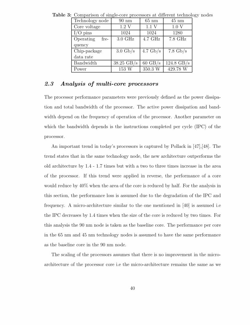
Table 3: Comparison of single-core processors at different technology nodesTechnology node 90 nm 65 nm 45 nmCore voltage 1.2 V 1.1 V 1.0 VI/O pins 1024 1024 1280Operating fre-quency
3.0 GHz 4.7 GHz 7.8 GHz
Chip-packagedata rate
3.0 Gb/s 4.7 Gb/s 7.8 Gb/s
Bandwidth 38.25 GB/s 60 GB/s 124.8 GB/sPower 153 W 350.3 W 429.78 W
2.3 Analysis of multi-core processors
The processor performance parameters were previously defined as the power dissipa-
tion and total bandwidth of the processor. The active power dissipation and band-
width depend on the frequency of operation of the processor. Another parameter on
which the bandwidth depends is the instructions completed per cycle (IPC) of the
processor.
An important trend in today’s processors is captured by Pollack in [47],[48]. The
trend states that in the same technology node, the new architecture outperforms the
old architecture by 1.4 - 1.7 times but with a two to three times increase in the area
of the processor. If this trend were applied in reverse, the performance of a core
would reduce by 40% when the area of the core is reduced by half. For the analysis in
this section, the performance loss is assumed due to the degradation of the IPC and
frequency. A micro-architecture similar to the one mentioned in [40] is assumed i.e
the IPC decreases by 1.4 times when the size of the core is reduced by two times. For
this analysis the 90 nm node is taken as the baseline core. The performance per core
in the 65 nm and 45 nm technology nodes is assumed to have the same performance
as the baseline core in the 90 nm node.
The scaling of the processors assumes that there is no improvement in the micro-
architecture of the processor core i.e the micro-architecture remains the same as we
40
move from one technology node to another. The transistor performance numbers are
taken from ITRS. Equation (28) gives the relation of the off-chip bandwidth to the
off-chip bus speed and the I/Os that carry these high speed signals. Assume that
the number of pins that carry these high speed signals is roughly 10% of all the I/O
pins in a particular technology node. For example, consider the 90 nm technology
node. Assuming that the chip operates at 3 GHz and that a seamless transition can
be provided from the chip to the package, the off-chip signal speed would be 3 Gb/s
and the number of I/O pins carrying these signals is 10% of 1024 [2]. Therefore, the
bandwidth associated with the single core processor is 38.25 GByte/s. Now consider
the 65 nm technology node, making the same assumptions as above and assuming
that the processor operates at 4.7 GHz. The bandwidth of the processor at this node
would be 59.925 GByte/sec The operating frequency at each node was obtained by
solving for the optimum operating point in terms of the threshold voltage, physical
parameters of a transistor and the frequency using the relations given in [2]. If we were
to use the scalable architecture approach [40] with four cores and use the same micro-
architecture as the 90 nm node without any increase in the frequency of operation,
the bandwidth in the 65 nm node would increase to ((38.25/1.42)) × 4 GByte/s,
which equals 78.06 GByte/s. This is greater than the bandwidth of a single- core
processor. This is assuming that the increase in the number of transistors as we move
from one technology node to another is used to increase the computational efficiency
rather than on-chip memory [41],[49]. The number of high speed I/Os required to
obtain this bandwidth of the chip would increase to 208. Using a similar approach
we could increase the bandwidth of the processor by using a larger number of cores.
The bottleneck in such an approach would be the total number of I/O pins on the
package. A reduction in the frequency of operation from 4.7 GHz to 3 GHz also
reduces the active power consumption from 130.894 W to 83.54 W. These numbers
were obtained from the analysis explained in the previous section. Using the above
41

Figure 24: Power dissipation, frequency of operation and bandwidth variation ofmulti-core processors through technology nodes.
multi-core approach it is possible to obtain a 1 TeraByte/s bandwidth in the future
technology nodes with a considerable savings in the power as shown in Fig. 24. An
example is discussed in this section.
The single-core processor in the 45 nm technology node dissipates 430 W of power
as per the calculations in the previous section. The active and static power com-
ponents are 195.217 W and 229.58 W respectively. The I/O power is described by
equation (18), as given in section 2.1 . The on-chip interconnect was modeled us-
ing the method described in [50]. The off-chip interconnect was modeled using the
HSpice interconnect models. A scaling factor of 30% based on [2] was applied for the
on-chip and off-chip interconnect capacitance through the technology nodes to get
the appropriate capacitance value for the 45 nm node. The power dissipation of the
I/Os calculated using equation (18) was 4.992 W.
Fig. 24 shows the power dissipation and bandwidth that can be achieved using the
multi-core approach for the 65 nm and 45 nm nodes. The analysis of the 45 nm node
will be presented here. As mentioned above the multi-core approach is used to reduce
42
the power and improve the bandwidth of the processor. The optimum operating point
in terms of the threshold voltage and frequency of operation is made based on the
relations given in [2]. The physical limits of a transistor such as gate oxide thickness
are constraints that limit the extent to which the threshold voltage and frequency
can be varied. In Fig. 22, it is observed that the major contributor to the power
dissipation is the static power. Therefore, the static power is reduced by increasing
the threshold voltage Vth. This leads to a decrease in the frequency of operation. The
optimal operating frequency of the processor was at 4 GHz, a decrease from 7.8 GHz
for a single processor. With the assumption made that the micro-architecture of the
processors does not improve, this core at 45 nm would be almost identical to the cores
in the preceding technology nodes. To obtain the 1 Terabyte/s number using eight
cores in the 45 nm technology node, the initial baseline assumption of 10% of all I/O
pins that carry high speed signals has been increased to 50% i.e the number of signal
lines that now carry these high data rates is 1280×0.5 = 640. By using the reasoning
mentioned earlier in the section, the bandwidth of 1 TeraByte/s was obtained using
eight cores, an increase from 124 GByte/s for a single-core processor. The bottleneck
for the 1 TeraByte/s would be the number of I/Os required on the package to sustain
such a high rate of data. The number of I/Os required to maintain 1 TeraByte/s
bandwidth with the chip to board data rate of 4 Gb/s is, 2000. Assuming a 50%
overhead of signal pins, the total number of signal pins would be 3000. The total
number of pins on the chip with 3000 signal I/Os is 9000, since the number of signal
pads are assumed to be one-third of the total pads in the chip [2]. The 9000 pins
include the power, ground and I/O pins. The total power dissipation of the eight core
processor is 107 W. The active power is close to 100 W, the static power dissipation is
negligible and the I/O power is 7 W. Table 4 below compares a single- core processor
with a multi-core processor for the 45 nm technology node.
The analysis for the number of metal levels and pins for the package are discussed
43
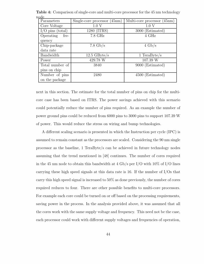
Table 4: Comparison of single-core and multi-core processor for the 45 nm technologynode
Parameters Single-core processor (45nm) Multi-core processor (45nm)Core Voltage 1.0 V 1.0 VI/O pins (total) 1280 (ITRS) 3000 (Estimated)Operating fre-quency
7.8 GHz 4 GHz
Chip-packagedata rate
7.8 Gb/s 4 Gb/s
Bandwidth 12.5 GByte/s 1 TeraByte/sPower 429.78 W 107.39 WTotal number ofpins on chip
3840 9000 (Estimated)
Number of pinson the package
2480 4500 (Estimated)
next in this section. The estimate for the total number of pins on chip for the multi-
core case has been based on ITRS. The power savings achieved with this scenario
could potentially reduce the number of pins required. As an example the number of
power ground pins could be reduced from 6000 pins to 3000 pins to support 107.39 W
of power. This would reduce the stress on wiring and bump technologies.
A different scaling scenario is presented in which the Instruction per cycle (IPC) is
assumed to remain constant as the processors are scaled. Considering the 90 nm single
processor as the baseline, 1 TeraByte/s can be achieved in future technology nodes
assuming that the trend mentioned in [48] continues. The number of cores required
in the 45 nm node to obtain this bandwidth at 4 Gb/s per I/O with 10% of I/O lines
carrying these high speed signals at this data rate is 16. If the number of I/Os that
carry this high speed signal is increased to 50% as done previously, the number of cores
required reduces to four. There are other possible benefits to multi-core processors.
For example each core could be turned on or off based on the processing requirements,
saving power in the process. In the analysis provided above, it was assumed that all
the cores work with the same supply voltage and frequency. This need not be the case,
each processor could work with different supply voltages and frequencies of operation,
44

which could lead to power savings. The above mentioned scenario’s are possible with
an improvement in the micro-architecture of the processors along with the continuing
historical trend in the improvement of transistor performance.
The above analysis shows that a multi-core approach to future processors can
improve the overall performance of processors. In order to support the bandwidth
that can be provided by these processors it is required that the packages have a
high density of I/Os. Also, the scaling of transistors leads to fine pitch interconnects
on silicon that are moving towards the nano scale. These fine features increase the
resistance of the wire, which leads to an increase in the loss and the RC delay. To
overcome this latency and loss, the wires can be moved onto the package with a
dielectric of low dielectric constant and low loss. The dimensions of the wires on the
package would be in the microns range and would lead to extremely high density
wiring on the package. To meet the decoupling requirements for on-chip circuits for
future processors, a large portion of the die would have to be used for fabricating
decoupling capacitors. This would lead to a reduction of valuable real estate for
transistors, which would decrease the computational logic of a processor. Embedded
decoupling capacitors on the package address this issue. The next section deals with
the packaging technologies that can meet the above requirements.
2.4 Packaging Platform
As highlighted in the previous sections multi-core processor packages would need to
support high number of I/Os. This requirement coupled with decoupling that needs
to be provided for the core and the I/Os puts stringent requirements on the design of
such packages. Real estate for putting surface mount capacitors for core decoupling
is an issue, since space is limited. Therefore, the approach would be to use embedded
capacitors for decoupling the core as well as the I/O circuits, which is the focus of
this thesis. Core decoupling can be achieved by placing individual thin/thick film
45

Figure 25: Cross section showing individual embedded capacitors for core decouplingin a package and embedded planar capacitors in a board for I/O decoupling.
capacitors in the package and I/O decoupling can be provided by using embedded
planar capacitors in the board as shown in Fig .25.
This section describes the enabling technologies that can provide a potential solu-
tion to the packaging issues in multi-core processors. Integral passives are becoming
increasingly important in realizing next generation electronics industry needs through
gradual replacement of surface mount components. The need for integral passives
emerges from the increasing demand for product miniaturization thus requiring com-
ponents to be smaller and packaging to be space efficient. The remaining part of
this chapter highlights the packaging platform required to support future multi-core
processor packages with high density I/Os and decoupling requirements.
2.4.1 Package details estimation
The number of metal levels and pins required for the 45 nm node multi-core processor
package is discussed in this section. The number of signal I/Os on the chip was
calculated to be 3000. With a 12.5 um width and spacing line, the pitch of the
interconnect is 25 um. Assuming the size of the solder bump is 50 um, the space
between the edges of the solder bump will be 75 um in a 125 um solder bump pitch.
46
Therefore, there would be three escape rows between two solder bumps. The number
of I/Os that can escape on the first metal layer is 1104. Therefore the number of metal
levels required for 3000 signal I/Os would be three. If there are two power ground
plane pairs with embedded discrete capacitors and a common power or ground plane,
and a ground plane between each signal layer, the number of metal planes needed
would be seven. The total number of metal planes required in the package will then
be 10. The number of pins and pin pitch at the bottom of the package will decide
its size. With 9000 chip pins, the package pins could be reduced to around 4500 i.e
3000 signal I/Os and 1500 power and ground pins. There need not be a one-to-one
correspondence between the pins on the chip and the number of pins at the bottom of
the package because of common power and ground buses within the package, which
reduces the number of power and ground pins on the bottom of the package. With a
0.5 mm board bump pitch, the size of the package would be 33.5 mm X 33.5 mm. It
is assumed here that the board bump technology can support high signal data rates.
The above calculation was based on the scenario listed in the ITRS regarding the
ratio of signal pins to power and ground pins. In the case of the multi-core processor
for the 45 nm node, the power dissipation is very less. Therefore the number of power
ground pins could be reduced to 3000. The total number of chip pins in this case
would then be 6000. Using the same reasoning as given above the number of pins at
the bottom of the package can be assumed to be 3500. The size of the package with
a 0.5 mm pitch would be 29.5 mm X 29.5 mm, a reduction of 250 mm2 in area as
compared to the earlier case. The above discussion is for a single multi-processor chip
on the package. In case of more than one multi-core processor chip, the number of
I/O pins in the package will increase. Assuming common power and ground buses for
both the chips in the package, the number of power and ground pins on the package
would be the same as for a single chip. With 4500 total pins on the bottom side
of the package as shown earlier in the section for a single chip, the total number of
47
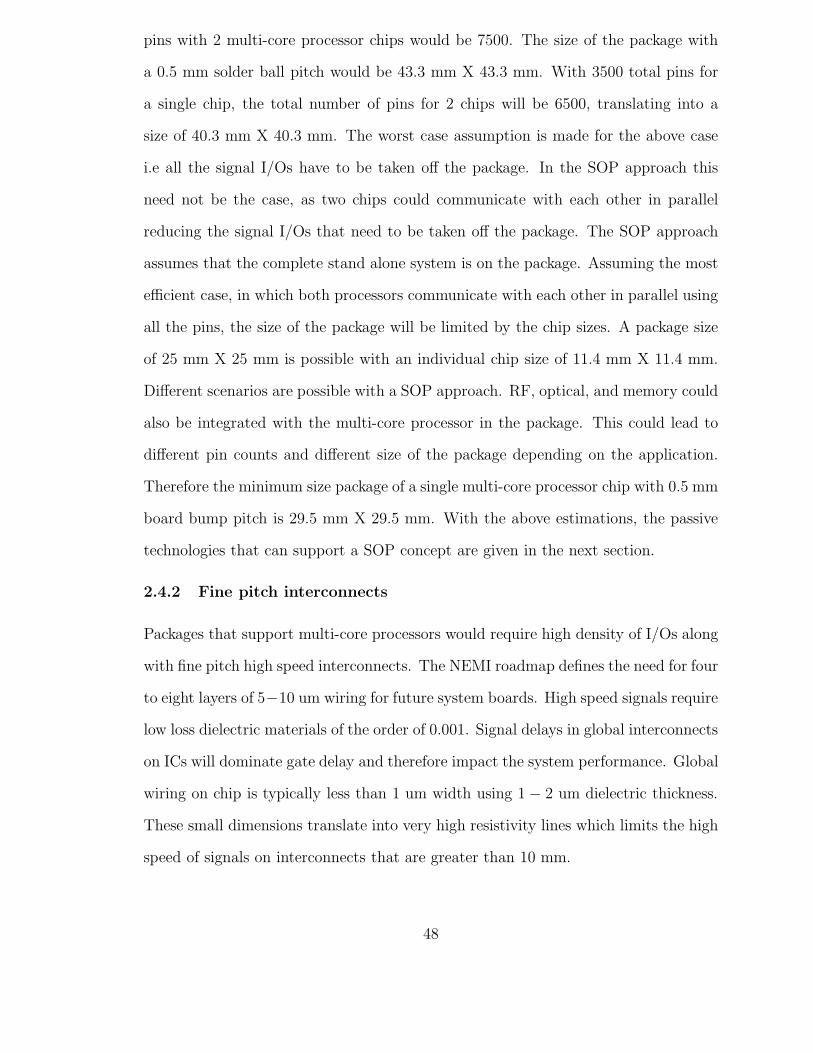
pins with 2 multi-core processor chips would be 7500. The size of the package with
a 0.5 mm solder ball pitch would be 43.3 mm X 43.3 mm. With 3500 total pins for
a single chip, the total number of pins for 2 chips will be 6500, translating into a
size of 40.3 mm X 40.3 mm. The worst case assumption is made for the above case
i.e all the signal I/Os have to be taken off the package. In the SOP approach this
need not be the case, as two chips could communicate with each other in parallel
reducing the signal I/Os that need to be taken off the package. The SOP approach
assumes that the complete stand alone system is on the package. Assuming the most
efficient case, in which both processors communicate with each other in parallel using
all the pins, the size of the package will be limited by the chip sizes. A package size
of 25 mm X 25 mm is possible with an individual chip size of 11.4 mm X 11.4 mm.
Different scenarios are possible with a SOP approach. RF, optical, and memory could
also be integrated with the multi-core processor in the package. This could lead to
different pin counts and different size of the package depending on the application.
Therefore the minimum size package of a single multi-core processor chip with 0.5 mm
board bump pitch is 29.5 mm X 29.5 mm. With the above estimations, the passive
technologies that can support a SOP concept are given in the next section.
2.4.2 Fine pitch interconnects
Packages that support multi-core processors would require high density of I/Os along
with fine pitch high speed interconnects. The NEMI roadmap defines the need for four
to eight layers of 5−10 um wiring for future system boards. High speed signals require
low loss dielectric materials of the order of 0.001. Signal delays in global interconnects
on ICs will dominate gate delay and therefore impact the system performance. Global
wiring on chip is typically less than 1 um width using 1 − 2 um dielectric thickness.
These small dimensions translate into very high resistivity lines which limits the high
speed of signals on interconnects that are greater than 10 mm.
48

The SOP approach would provide the opportunity for global wires on-chip to be
integrated on the package if line widths of the order of 10−13 um are made available
using thin dielectric films. With a dielectric constant of four, 50 Ω characteristic
impedance for a 12.5 um wide line can be achieved if the thickness of the dielectric
is 7.5 um. Line widths in the range of 3− 5 um will further reduce the total number
of signal levels, the thickness of the dielectric and therefore the total thickness of the
package. The typical methodologies used to increase wiring density are: 1) reducing
the line width and line space; 2) increasing the number of layers and, 3) using small
capture pads. The research at Packaging Research Center (PRC) is focused on all of
these including 1) ultra-fine lines of 3 − 5 m dimensions, and 2) stacked microvias of
10 − 15 m diameter. Precise control of the photolithography process combined with
high resolution liquid photoresists coated as thin films has been used to achieve copper
lines with less than 5% control of X, Y and Z dimensions. With the technologies that
are being developed, the wiring density of future packages can be met. For example,
consider the 45 nm node in which it was estimated that the total number of pins on
chip would be 9000. If the pins were to be distributed evenly on a package of size
140 mm2, the pitch required would be approximately 125 um. An example of fine
pitch routing for 100 m pitch flip chip packages is shown in Fig. 26, which illustrates
two lines per channel using 12 m lines/spaces fabricated on build-up layers on an FR-4
substrate. Planar embedded capacitors are useful in providing low impedance to the
return current, which enables decoupling high speed I/O’s as shown in Chapter 5.
2.4.3 Microvias
A novel low cost process for fabricating multilayer stacked via structures has been
developed using a panel electroplating and subtractive etch process called P2ES (panel
plating etched stud) [51]. Filled stacked vias of 50 um, 75 um and 100 m diameter up
to four metal layers have been demonstrated using this low cost large area approach.
49
Figure 26: Two 12 um lines through a 100 um pitch flip chip.
Stud height uniformities of less than 1 m have been demonstrated using this technique
on 300 mm x 300 mm FR-4 substrates. The stacked via structure along with the ultra-
fine lines can potentially meet the interconnection and global wiring requirements of
next generation SOP packages.
2.4.4 Embedded Capacitors
Among various passive devices, capacitors are the hardest to integrate owing to non-
availability of material systems to cover the range of capacitances required to provide
decoupling over the entire frequency band for today’s systems. With the trend to-
wards higher power and lower voltage, clean power has to be supplied to the integrated
circuits. Decoupling capacitors act as reservoirs of charge and supply the transient
currents for the switching circuits, reducing the switching noise. On-chip decoupling
capacitance with negligible parasitic inductance provides the lowest power supply
impedance at high frequencies. Thin oxides are generally used to supply the capac-
itance on-chip though they occupy valuable silicon real estate leading to trade-offs
in chip area, cost and noise tolerance. To reduce the decoupling capacitance burden
50
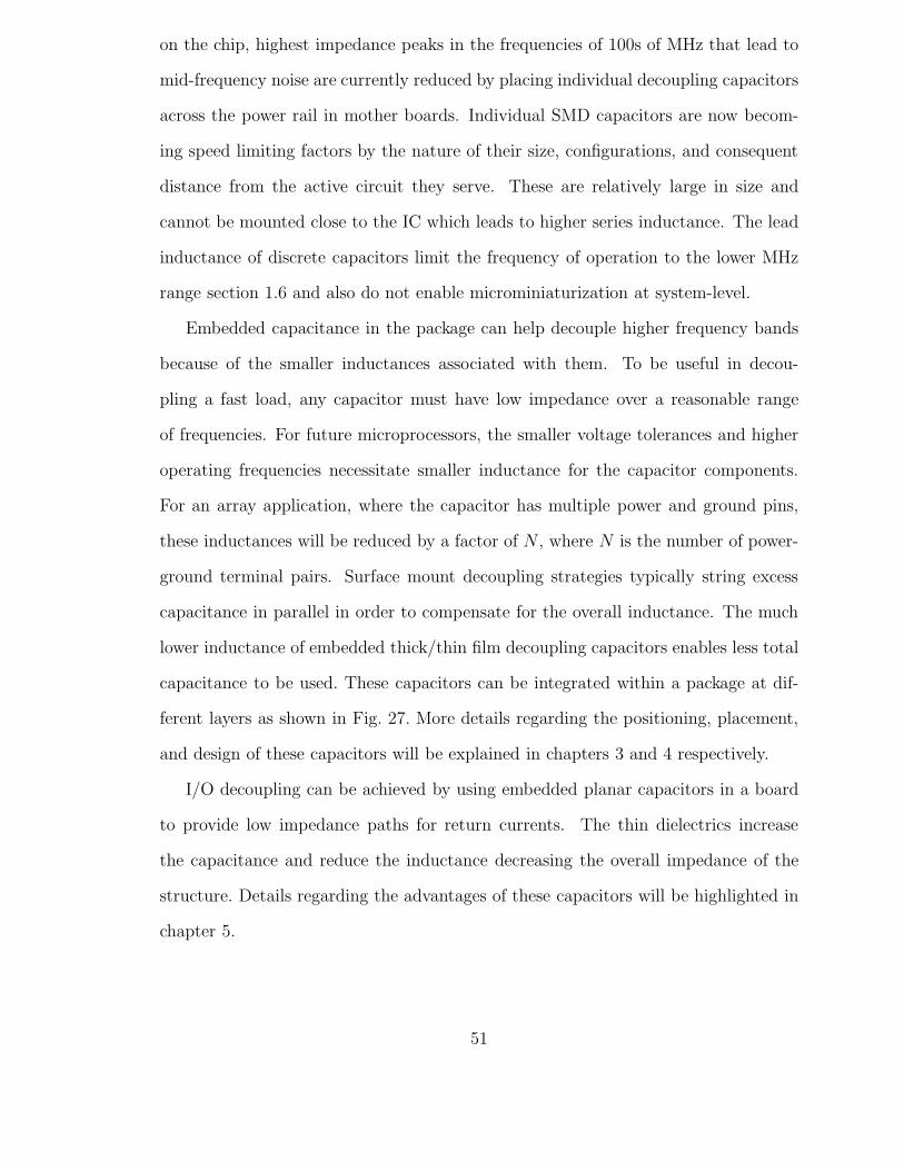
on the chip, highest impedance peaks in the frequencies of 100s of MHz that lead to
mid-frequency noise are currently reduced by placing individual decoupling capacitors
across the power rail in mother boards. Individual SMD capacitors are now becom-
ing speed limiting factors by the nature of their size, configurations, and consequent
distance from the active circuit they serve. These are relatively large in size and
cannot be mounted close to the IC which leads to higher series inductance. The lead
inductance of discrete capacitors limit the frequency of operation to the lower MHz
range section 1.6 and also do not enable microminiaturization at system-level.
Embedded capacitance in the package can help decouple higher frequency bands
because of the smaller inductances associated with them. To be useful in decou-
pling a fast load, any capacitor must have low impedance over a reasonable range
of frequencies. For future microprocessors, the smaller voltage tolerances and higher
operating frequencies necessitate smaller inductance for the capacitor components.
For an array application, where the capacitor has multiple power and ground pins,
these inductances will be reduced by a factor of N , where N is the number of power-
ground terminal pairs. Surface mount decoupling strategies typically string excess
capacitance in parallel in order to compensate for the overall inductance. The much
lower inductance of embedded thick/thin film decoupling capacitors enables less total
capacitance to be used. These capacitors can be integrated within a package at dif-
ferent layers as shown in Fig. 27. More details regarding the positioning, placement,
and design of these capacitors will be explained in chapters 3 and 4 respectively.
I/O decoupling can be achieved by using embedded planar capacitors in a board
to provide low impedance paths for return currents. The thin dielectrics increase
the capacitance and reduce the inductance decreasing the overall impedance of the
structure. Details regarding the advantages of these capacitors will be highlighted in
chapter 5.
51

Figure 27: Cross section showing the placement of embedded capacitors in a pack-age.
2.5 Summary
The power dissipation trends of processors has been captured in this chapter by
developing models to capture the active and static power dissipation trends. The
analysis of multi-core processors has been shown to improve overall performance i.e
an increase in the off-chip bandwidth and decrease in power dissipation of processors.
A description into the packaging platform required to support high density I/Os to
support future processors has also been investigated in this chapter. The rest of this
thesis investigates the measurement, modeling, characterization, and performance of
the individual embedded capacitors developed at the PRC using the hydrothermal
process and capacitors fabricated by DuPont. These capacitors are primarily used for
core decoupling high performance circuits. The performance of embedded planar ca-
pacitors fabricated by DuPont in decoupling I/O circuits by providing low impedance
to the return current of I/O signals has also been investigated in this thesis.
52

CHAPTER III
DESIGN AND CHARACTERIZATION OF INDIVIDUAL
EMBEDDED PACKAGE CAPACITORS
The advantages of using discrete thin/thick film capacitors was briefly mentioned in
chapter 1. An analysis into the performance improvements using these capacitors is
presented in this section. As an illustration of the concept, a simulation of the per-
formance of a decoupling array with the DuPont capacitors within a package was
performed. Fig. 29 shows the performance of an embedded decoupling network that
can be designed to provide decoupling at frequencies above 100 MHz and can target
impedances of the order of 1 mΩ as compared to the profile shown in Fig. 15. Care
was taken that all the capacitors were placed directly under or around the processor
to minimize the effect of the spreading inductance of the power ground planes. The
different sized capacitors that were used to obtain the impedance profile shown in
Fig. 29 were placed in two discrete capacitor layers within a package. The details
regarding the package stack up are presented in section 4.1. 25 1.2 mm × 1.2 mm
capacitors along with 25 0.5 mm × 0.5 mm capacitors were used to target the lower
frequency band. The higher frequency band was targeted using 25 1.2 mm × 1.2 mm
capacitors and 42 0.75 mm capacitors. The two combinations of 1.2 mm × 1.2 mm
capacitors were placed in different levels of the package. Due to their different place-
ment, the via inductances associated with each combination were different and they
therefore resonate at different frequencies. This analysis was done to show the ad-
vantages of using embedded capacitors and by proper selection of the sizes of the
capacitor the mid-frequency band from 100 MHz to 2 GHz can be targeted for de-
coupling. The rest of this chapter is organized as follows 1) The description of the
53

Figure 28: Discrete capacitor layer in the package
106
107
108
109
1010
10−4
10−3
10−2
10−1
100
101
frequency (Hz)
Impe
danc
e(O
hms)
1.2mm X 1.2mm
0.75mm X 0.75mm
0.5mm X0.5mm
1.2mm X1.2mm
Figure 29: Impedance profile with embedded capacitors in the package
54

capacitor structures which includes the design, shape and the material properties will
be presented; 2) The modeling methodology used to model these structures is high-
lighted in this chapter; 3) The measurement and characterization of the thin/thick
film embedded capacitors is explained. A detailed analysis into the self and transfer
impedance measurement methodology used to characterize these capacitors will be
presented; 4) The model to hardware correlation of the results is also highlighted in
this chapter.
3.1 Description of capacitor structures
This section highlights the properties of the different materials used as dielectrics for
the embedded capacitors. The first material is a thin film hydrothermal based barium
titanate capacitor manufactured at the Packaging Research Center(PRC) [52].
A brief description into the process used to fabricate the capacitors is presented in
this part of the section. These capacitors are fabricated on laminated copper foils using
low cost and low temperature(< 100oC) hydrothermal process. The copper laminate is
clad with Titanium and treated with Barium ions (Ba+2) in highly alkaline solution
at 95oC. The resultant Barium Titanate film is 300 nm thick and has a dielectric
constant of 300. The top electrode is 2 um thick copper. The loss tangent of the
material is less than 0.06 and the capacitance density is of the order of 1 µF/cm2.
The thickness of the grain sizes of barium titanate in the dielectric vary from 60 nm
to 80 nm. The cross section of a barium titanate capacitor is shown in Fig 30. The top
electrode is 2 um thick copper and the bottom electrode is 12 um thick copper with
500 nm thick titanium as shown in Fig 30. Square capacitors of size 1 mm×1 mm
that were fabricated and measured are shown in Fig. 31.
The other material investigated is a thick film capacitor material from DuPont.
The thickness of the dielectric is 20 um and the dielectric constant is 3000. The ca-
pacitance density is of the order of 1.328 nF/mm2 and the loss of the dielectric is less
55

Figure 30: Cross section of capacitors fabricated at PRC using the hydrothermalprocess.
Figure 31: Fabricated square barium titanate capacitors.
56

Figure 32: Cross section of DuPont’s embedded capacitor.
than 0.01 at 1 MHz. The cross-section of the capacitor fabricated by DuPont is shown
in Fig 32 and a snapshot of the actual capacitor embedded in BT laminate is shown in
Fig 33. Different size capacitors were designed and fabricated as shown in Fig. 34. A
brief description of the fabrication process of these capacitors is presented in this sec-
tion. The process uses a fired-on-foil approach. A thick film capacitor dielectric and
electrode paste is screen printed on to the copper foil in the location desired in the
circuit and fired in nitrogen at approximately 900oC to form the fired-on-foil compo-
nents. Following this, the foil maybe treated to improve adhesion to prepeg and then
it is bonded component face down, into a laminate structure used to fabricate inner-
layers for a multi-layer printed wiring board. The inner layer is then etched to form
the capacitor electrodes from the copper foil. Following this, the inner layer may re-
ceive additional treatment before it is incorporated inside a multi-layer printed wiring
board [53]. The placement of these capacitors in the package was previously shown
in Fig 27 in chapter 1. This chapter investigates the design, characterization, and
modeling of the thin/thick film discrete embedded capacitors.
3.2 Measurement and Characterization of capacitors
A two port frequency domain measurement methodology was used to measure the
impedance of the capacitive structures [54]. One port measurements are usually
57
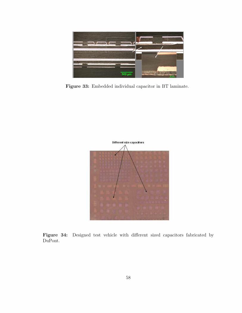
Figure 33: Embedded individual capacitor in BT laminate.
Figure 34: Designed test vehicle with different sized capacitors fabricated byDuPont.
58

inaccurate when measuring low impedance structures of the orders of 10′s of mΩ.
This is because near the resonant frequency of the structure, the value of the reflection
coefficient is close to −1. This can be explained as follows; the reflection coefficient
is given as:
Γ =ZL − ZO
ZL + ZO(29)
The system impedance of the VNA is 50 Ω , and if the structure has an impedance
in the mΩ range at frequencies close to the resonant frequency, then from the above
formula all the energy will be reflected back and the readings will be very noisy. An-
other important source of error in one port measurements is the contact resistance
of the probe when it touches the structure. This value of resistance depends on the
contact and could vary for different measurements i.e it is not repeatable. The con-
tact resistance ends up in series with the impedance of the structure and adds to the
inaccuracy of the readings.
To overcome the above limitations of a one port measurement, two ports are gener-
ally used to measure power plane structures. The advantage of two port measurements
is that the impedance of the structure is extracted from the S21 parameters rather
than S11 or S22. The advantage being that the discontinuities that were present in
the one port measurement were in series with the device under test (DUT). In the two
port measurement methodology the resistance and inductance due to the discontinu-
ity are in series with the 50Ω system impedance of the VNA and the following sections
in this chapter will highlight the error introduced by these discontinuities, which are
negligible. Since, the impedance of the DUT is extracted from the S21 measurements,
an approximation to a one port reading can be done if the two ports are placed very
close to each other. The method will be briefly described in this section.
The measurement equipment included Agilent’s 8720ES vector network analyzer (VNA)
with a bandwidth of 50 MHz to 20.5 GHz and 500 um GS-SG cascade probes. A stan-
dard short,open,load, and thru SOLT calibration was carried out on the probes using
59

Figure 35: The equivalent circuit of the measurement showing the discontinuitywith the two ports placed very close to each other.
the ISS substrates.
3.2.1 Self Impedance Measurement
The basic equations used to characterize these structures is explained: For the self
impedance measurement of the DUT, the two probes connected to the VNA are placed
very close to each other. The equivalent circuit diagram by including the parasitics
is shown in Fig. 35.
The S matrix can be obtained by using the transformation equations. The trans-
formation equation used to convert the Z parameters to the S parameters is as fol-
lows [55]:
S21 =2 × Z12 × ZO
(Z11 + Z0)(Z22 + Z0) − Z12Z21
(30)
The above equations are modified based on the discontinuities. The discontinuities
can be expressed as:
Z1 = R1 + jωL1 (31)
60

and
Z2 = R2 + jωL2 (32)
Where R1, R2 and L1, L2 are the contact resistances and inductances between the
probe and the DUT. From Fig. 35, Z11 and Z22 are derived from the Z parameter
equations and are ZDUT + R1 + jωL1 and ZDUT + R2 + jωL2 respectively. S21 is
derived by using the standard conversion factor
S21 =2 × Z12 × ZO
(Z11 + ZO)(Z22 + ZO) − Z12 × Z21(33)
Substituting the values for Z11, Z22 and Z12, we get the following equation for S21.
S21 =2ZDUTZO
(ZDUT + R1 + jωL1 + ZO)(ZDUT + R2 + jωL2 + ZO) − ZDUT × ZDUT(34)
where Z12=Z21=ZDUT . Further simplifying equation 34 by assuming that ZO >>
R1 and ZO >> R2
S21 =2 × ZDUT × ZO
(ZDUT + jωL1 + ZO)(ZDUT + jωL2 + ZO) − Z12 × Z21(35)
Solving for ZDUT from the above equation we get
ZDUT =S21
2
Z1 × Z2
(ZO − S12 (Z1+Z2)2
)(36)
Where Z1 and Z2 are ZO+jωL1 and ZO+jωL2 respectively. The error introduced due
to the discontinuities is calculated by making an assumption that Z1=Z2. Equation 36,
reduces to
ZDUT =S21
2
Z1ZO
Z1
− S21(37)
Assuming that the inductance due to the discontinuity is 0.2 nH equation 37 can be
rewritten as:
ZDUT =S21
2
(50 + jω × 0.2 × 10⁻⁹)
( 5050+jω×0.2×10⁻⁹ − S21)
(38)
The error introduced by the discontinuity will be less for low impedance structures.
From equation 38, it is evident that the error is dependent on the measurement
61

Figure 36: Measurement set up using 2 ports of the VNA
frequency range. At 10 GHz, the ( 5050+jω×0.2×10⁻⁹ ) term is equal to 0.97. For the error
analysis, the denominator is assumed to be 1 − S21. At 10 GHz, the numerator =
51.55, therefore equation 38 reduces to the following.
ZDUT = 25.77 ∗ S21
1 − S21(39)
The error introduced from the above equation is 3% when compared to the equa-
tion 41, which is derived without the effect of discontinuity. For low values of S21,
the error introduced would be lower.
Therefore, this part of the section derives the equations used to calculate the
impedance profile of the DUT by neglecting the effect of the discontinuities. The
equivalent circuit by ignoring the effect of the discontinuity is shown in Fig. 36. The
structures can be characterized by assuming a ”T” network approach as shown in
Fig. 37. Z11 = Z22 = Z12 since the two probes are placed very close to each other
on the DUT. Therefore, Fig. 37 can be approximated as Fig. 38. All the elements of
the two port Z matrix will be equal to each other.
In the above equation Z0=50Ω, is the impedance of the VNA. The resultant
expression for S21 by substituting for Z11 = Z22 = Z12 = ZDUT is as follows:
62
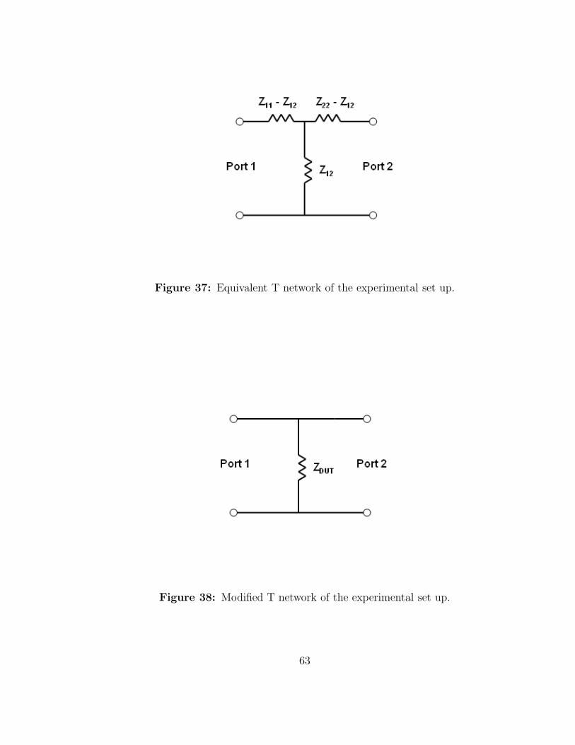
Figure 37: Equivalent T network of the experimental set up.
Figure 38: Modified T network of the experimental set up.
63

S21 =2ZDUT ZO
(Z + Z0)2 − Z2DUT
(40)
Where Z0 = 50 Ω and solving the above equation for ZDUT we obtain the following
equation:
ZDUT = 25 ∗ S21
1 − S21(41)
Be separating the real and imaginary parts of ZDUT and S21, the equations listed
below are obtained.
ReZ(dut) = 25 × (Re(S21) × (1 − Re(S21)) − Img(S21)2)
((1 − Re(S21)2) + Img(S21)2)(42)
ImZ(dut) = 25 × Img(S21)
((1 − Re(S21)2) + Img(S21)2)(43)
Where ReZ(dut) and ImZ(dut) are the real and imaginary parts of the device under
test. The above equations were used to characterize the impedance profile of the
individual thin/thick film capacitors highlighted in this thesis.
3.2.1.1 Error Analysis
This part of the section investigates error introduced due to via discontinuities. The
via can be assumed to be modeled as a series combination of a resistor and an in-
ductor. As done in the previous part of this subsection, the following is assumed: ZO
>> R1 and ZO >> R2, where R1 and R2 are the resistances of the vias. The self
impedance is calculated by using reflection theory since the reference impedance has
changed from 50Ω to Z1 and Z2, where Z1 and Z2 are ZO + jωL1 and ZO + jωL2
respectively. L1 and L2 are the series inductances of the vias. S11 can be calculated
as follows:
S11 =
ZDUT×Z2ZDUT +Z2
− Z1ZDUT×Z2ZDUT +Z2
+ Z1(44)
64

also S21 = 1 + S11, solving for S12 and rearranging to get ZDUT , the following
expression is obtained.
ZDUT = S21(Z1
2)
1
1 − S21(Z1+Z12Z2
)(45)
The above equation can be rewritten to analyze the error introduced because
of the discontinuity. For this analysis assume that Z1 = Z2 = ZO + jωL. L is the
inductance due to the discontinuity and is assumed to be 0.2 nH. Equation 45, reduces
to the following:
ZDUT = S21(Z1
2)
1
1 − S21(46)
Equation further reduces to the following
ZDUT = S21 × 25(1 + jως
1 − S21) (47)
ς is L50
, therefore the error introduced by measuring a structure with an impedance of
0.2Ω at 10 GHz with 0.2 nH of inductance is close to 3%. This error analysis is similar
to the analysis carried out in [56]. However, the error introduced by the vias depend
on the thickness of the board and the frequency range over which the measurement is
carried out. The error introduced may be significant for thick boards with vias that
span the depth of the board.
3.2.2 Transfer Impedance Measurement
Extraction of the transfer impedance from the S21 measurements can also be done
and is shown in the following analysis. If the probes are placed a certain distance
apart from each other then Z11 6=Z22 6=Z12, therefore, equation 36 derived for the
extraction of the self impedance cannot be used in this situation. The model used for
the following analysis is shown in Fig. 37. By including discontinuities in the analysis
the equivalent ”T” network is modified as shown in Fig. 39. Z11 and Z22 can be
derived from the standard definitions of the Z parameters. From Fig. 39, Z11 and
65

Figure 39: The equivalent circuit of the measurement showing the discontinuitywith the two ports placed far apart from each other.
Z22 are Z11 + R1 + jωL1 and Z22 + R2 + jωL2 respectively. By using the standard
conversion of S21 to Z parameters we obtain the following equation.
S21 =2Z12ZO
(Z11 + R1 + jωL1 + ZO)(Z22 + R2 + jωL2 + ZO) − Z122(48)
Assuming that ZO >> R1 and ZO >> R2, the above equation reduces to the following.
S21 =2Z12ZO
(Z11 + Z1)(Z22 + Z2) − Z122(49)
Solving the above equation, the following equation is obtained for Zij.
Zij =(S21 × Z1 × Z2)
2
(1 + Z11Z1
)(1 + Z22Z2
)
(ZO + S21Z122
)(50)
For low impedance power plane structures, Z2 >> Z22,Z1 >> Z11, and ZO≈Z1≈Z2
. Therefore, equation 50 can be reduced to the following:
Zij ≈ S21 × 25 (51)
The above equation was used to characterize the transfer impedance characteristics of
the DUT in this thesis. This analysis highlights the negligible effect of discontinuities
66

on the transfer impedance measurements on low impedance structures using the two
port methodology.
Assume that there are no discontinuities involved in the transfer impedance mea-
surement. Therefore, by using the standard conversion for S12 to Z parameters we
obtain
S21 =2Z12ZO
(Z11 + ZO)(Z22 + ZO) − Z122(52)
Solving for Zij, the following equation is obtained.
Zij =S21
2
(Z11 + 50)(Z22 + 50)
(ZO + S21Z122
)(53)
Also, assuming that 50>>Z11, 50>>Z22 and ZO>> S21Z122
, the above equation
reduces to equation 51.
This part of the section investigates the variation in the transfer impedance mea-
surements because of the via discontinuities. The via discontinuities are modeled by
a series combination of resistors and inductors. As done in the previous part of
this subsection, the following is assumed: ZO >> R1 and ZO >> R2. The transfer
impedance is calculated by using reflection theory since the reference impedance is
no longer 50Ω. S11 can be calculated as follows:
S11 =
(Z11×Z22+Z11×Z2−Z122)Z22+Z2
− Z1(Z11×Z22+Z11×Z2−Z122)
Z22+Z2+ Z1
(54)
Where Z1 and Z2 are 50+jωL1 and 50+jωL2 respectively. Solving for S21 = 1+S11,
and then for Zij, the following equation is obtained.
Zij =
√
S21 × (Z1)(Z2) − 2 × (Z11)(Z2)
(S21 − 2)(55)
The above equation was obtained by assuming that Z1>>Z11 and Z2>>Z22.
3.2.3 Measurement and characterization set up
The measurement set up for characterizing the capacitive structure is shown in Fig. 40.
Probe 1 is the transmitter and probe 2 measures the voltage drop across the device
67

Figure 40: The measurement set up for characterizing the capacitors.
109
1010
10−2
10−1
100
Frequency(Hz)
Impe
danc
e(O
hms)
Meas1Meas2Meas3
Figure 41: Comparison of three different measurement results on the same capacitor.
in one measurement cycle. The functions of the ports are reversed in the next mea-
surement cycle of the VNA. S21 is the insertion loss measured across the device at
each frequency point. By calculating the real and imaginary parts of the device the
Using equation 41, impedance profile over the measured frequency band can be ob-
tained. The robustness and repeatability of this measurement technique was done by
carrying out a number of measurements on the same test capacitor. The square test
capacitor was fabricated at the PRC using the hydrothermal process and the dimen-
sions of the capacitor were 0.75 mm × 0.75 mm. The results are shown in Fig. 41 for
three different measurements done with different calibrations. The repeatability of
the technique is apparent from the results in the figure. The capacitance, inductance,
and resistance were extracted from the measurements and are plotted in Fig’s 43, 43,
68
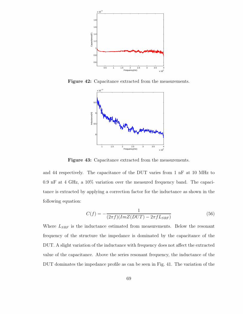
0.5 1 1.5 2 2.5 3 3.5 4
x 109
0.6
0.8
1
1.2
1.4
1.6
1.8
x 10−9
Frequency(Hz)
Cap
acita
nce(
F)
Figure 42: Capacitance extracted from the measurements.
1 1.5 2 2.5 3 3.5 4
x 109
8
8.5
9
9.5
x 10−12
Frequency(Hz)
Indu
ctan
ce(H
)
Figure 43: Capacitance extracted from the measurements.
and 44 respectively. The capacitance of the DUT varies from 1 nF at 10 MHz to
0.9 nF at 4 GHz, a 10% variation over the measured frequency band. The capaci-
tance is extracted by applying a correction factor for the inductance as shown in the
following equation:
C(f) = − 1
(2πf)(ImZ(DUT ) − 2πfLSRF )(56)
Where LSRF is the inductance estimated from measurements. Below the resonant
frequency of the structure the impedance is dominated by the capacitance of the
DUT. A slight variation of the inductance with frequency does not affect the extracted
value of the capacitance. Above the series resonant frequency, the inductance of the
DUT dominates the impedance profile as can be seen in Fig. 41. The variation of the
69
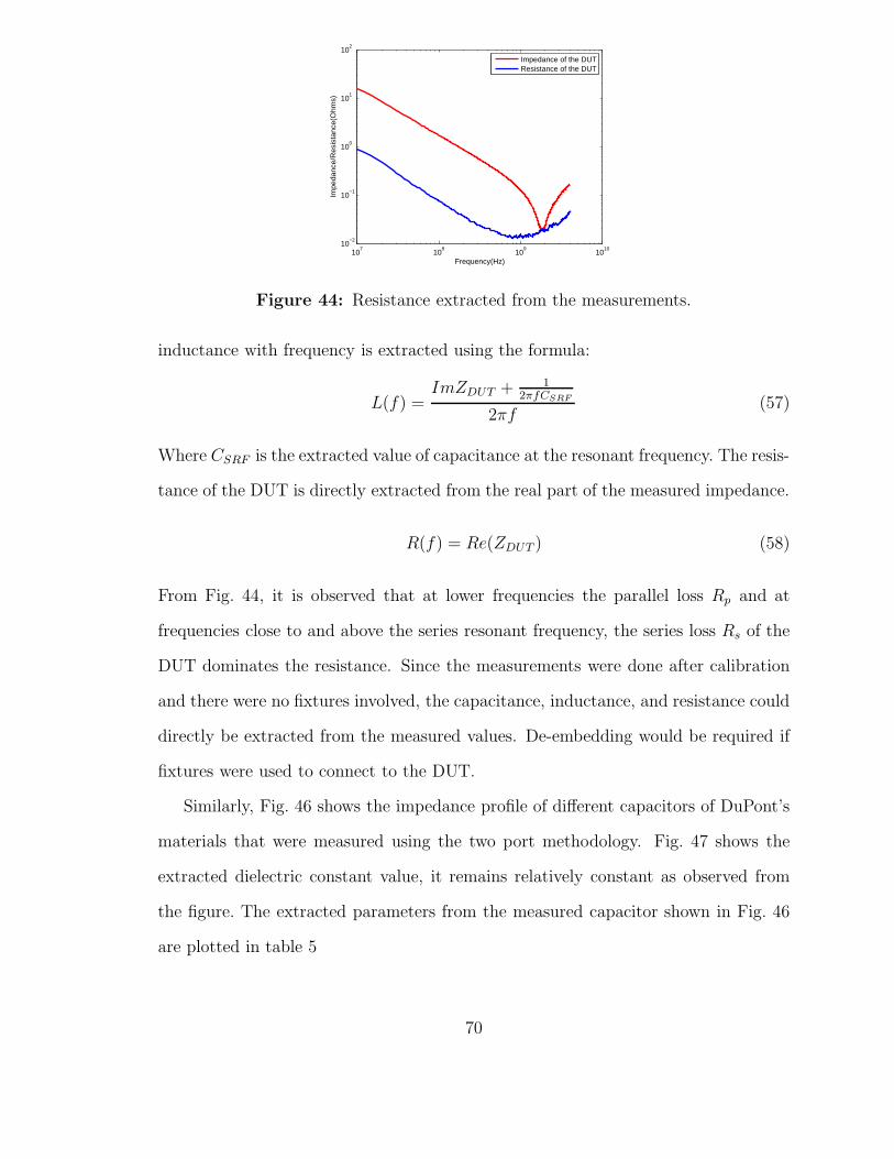
107
108
109
1010
10−2
10−1
100
101
102
Frequency(Hz)
Impe
danc
e/R
esis
tanc
e(O
hms)
Impedance of the DUTResistance of the DUT
Figure 44: Resistance extracted from the measurements.
inductance with frequency is extracted using the formula:
L(f) =ImZDUT + 1
2πfCSRF
2πf(57)
Where CSRF is the extracted value of capacitance at the resonant frequency. The resis-
tance of the DUT is directly extracted from the real part of the measured impedance.
R(f) = Re(ZDUT ) (58)
From Fig. 44, it is observed that at lower frequencies the parallel loss Rp and at
frequencies close to and above the series resonant frequency, the series loss Rs of the
DUT dominates the resistance. Since the measurements were done after calibration
and there were no fixtures involved, the capacitance, inductance, and resistance could
directly be extracted from the measured values. De-embedding would be required if
fixtures were used to connect to the DUT.
Similarly, Fig. 46 shows the impedance profile of different capacitors of DuPont’s
materials that were measured using the two port methodology. Fig. 47 shows the
extracted dielectric constant value, it remains relatively constant as observed from
the figure. The extracted parameters from the measured capacitor shown in Fig. 46
are plotted in table 5
70
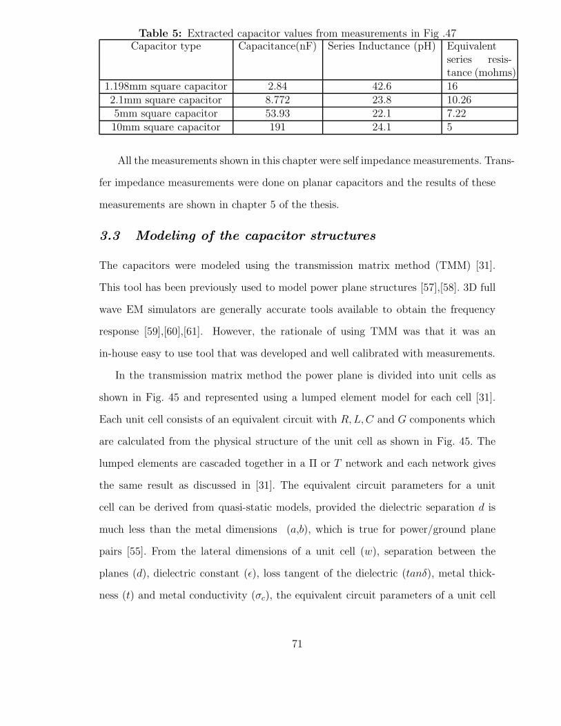
Table 5: Extracted capacitor values from measurements in Fig .47Capacitor type Capacitance(nF) Series Inductance (pH) Equivalent
series resis-tance (mohms)
1.198mm square capacitor 2.84 42.6 162.1mm square capacitor 8.772 23.8 10.265mm square capacitor 53.93 22.1 7.2210mm square capacitor 191 24.1 5
All the measurements shown in this chapter were self impedance measurements. Trans-
fer impedance measurements were done on planar capacitors and the results of these
measurements are shown in chapter 5 of the thesis.
3.3 Modeling of the capacitor structures
The capacitors were modeled using the transmission matrix method (TMM) [31].
This tool has been previously used to model power plane structures [57],[58]. 3D full
wave EM simulators are generally accurate tools available to obtain the frequency
response [59],[60],[61]. However, the rationale of using TMM was that it was an
in-house easy to use tool that was developed and well calibrated with measurements.
In the transmission matrix method the power plane is divided into unit cells as
shown in Fig. 45 and represented using a lumped element model for each cell [31].
Each unit cell consists of an equivalent circuit with R, L, C and G components which
are calculated from the physical structure of the unit cell as shown in Fig. 45. The
lumped elements are cascaded together in a Π or T network and each network gives
the same result as discussed in [31]. The equivalent circuit parameters for a unit
cell can be derived from quasi-static models, provided the dielectric separation d is
much less than the metal dimensions (a,b), which is true for power/ground plane
pairs [55]. From the lateral dimensions of a unit cell (w), separation between the
planes (d), dielectric constant (ǫ), loss tangent of the dielectric (tanδ), metal thick-
ness (t) and metal conductivity (σc), the equivalent circuit parameters of a unit cell
71

Figure 45: Unit cell and equivalent circuit ( T and Π models).
can be computed as follows:
C =ǫoǫrw
2
d(59)
L = µod (60)
Gd = ωCtanδ (61)
RDC =2
σct(62)
RAC = 2
√
πfµo(1 + j)
σc
(63)
Equations 59, 60, and 61 have been previously introduced in chapter 1 of this
thesis. In the above equations ǫo is the permittivity of free space, µo is the permeability
of free space and ǫr is the relative permittivity of the dielectric. The parameter RDC is
the resistance of both the power and ground planes for a steady DC current, where the
planes are assumed to be of uniform cross section. The AC resistance RAC accounts for
the skin effect on both conductors. The shunt conductance Gd represents the dielectric
loss in the material between the planes. In modeling the capacitive structures the
fringing effects have been ignored because of the large aspect ratio of these structures.
The measurement and modeling results of a 2.1 mm diameter circular and a 1 mm a
side square barium titanate capacitor are shown in Fig. 48. The modeled result of a
Dupont capacitor of size 2 mm × 2 mm is shown in Fig .49. Ports were appropriately
72

Figure 46: The impedance profiles of different sized capacitors.
Figure 47: The variation of dielectric constant with frequency.
73

Figure 48: Measured and modeled impedance profiles of BaTiO3 capacitors.
defined in the model to get the correct model to hardware correlation. The definition
of the ports corresponded to the exact coordinates of the probes on the measurement
structure. The parasitic inductance of the probe set up had to be included in the
model to get a good correlation between the model and measurement. The details of
the parasitic inductance extraction and model to hardware correlation are also given
in [62].
The hydrothermal capacitor measurement results of a 1 mm × 1 mm and 2.1 mm
diameter capacitor using the method described above are shown in Fig. 50 and Fig. 55
respectively. The measurements were done by placing 500 um pitch GS and SG probes
75 um apart from each other. The initial modeling result of the 1 mm capacitor is
shown in Fig. 51. The structure resonates at 1.23 GHz. The capacitance of the
structure is 9 nF. The equivalent series inductance (ESL) and series resistance (ESR)
of the capacitor according to the modeling is 1.85 pH and 16.9 mohms respectively.
As can be seen by comparing the initial model to the measurement, there is a large
discrepancy in the results. In order to match the measurement results, the inductance
associated due to the probes was extracted from the measurement set up. This was
done by placing both the probes on the ground electrode exactly the same distance
74

Table 6: Extracted capacitor values from measurementsCapacitor type Capacitance(nF) Series
Induc-tance (pH)
Equivalentseries resis-tance (mohms)
ResonantFrequency(MHz)
1mm square capacitor 9 38 16.9 272.142.1mm diameter circle 27.9 35 20 161.05
apart as they were on the device under test. The extracted inductance between the
probes is shown in Fig. 52. The model was compensated for by defining two ports
75 um apart and including the extracted inductance of 37.5 pH to the impedance
between the ports. The correlation of the hardware to the new model is shown in
Fig. 53. The capacitance of the structure was extracted and is plotted in Fig .54. The
measurement and modeling result of a 2.1 mm diameter circular capacitor is shown
in Fig .55 and Fig .56 respectively. The capacitance of the structure is 27.9 nF and
the ESR is approximately 20 mΩ. In order to match the model to the hardware, the
inductance associated with the probes was extracted as done earlier. The spacing
between the probes was also 75 um in this case. The extracted inductance is shown
in Fig .57, this inductance value was included in the model and the correlation be-
tween the updated model and measurement is shown in Fig .58. The capacitance of
the structure was extracted and is plotted in Fig .59. Fig .60 shows the comparison
between the measured values of different sized capacitors. The dimensions of the
structures are 0.9 mm square, 1 mm square, and a 2.1 mm diameter circular capac-
itor. The measurement results show that the impedance responses of the capacitive
structures are extremely sensitive to the probe inductances.
The extracted results of the 1mm × 1mm square and 2.1mm diameter hydrother-
mal (thin film) capacitor is summarized in table 6.
75

Figure 49: Model to hardware correlation of a 2 mm × 2 mm Dupont capacitor.
Figure 50: Measured frequency response of a 1 mm × 1 mm hydrothermal capacitor.
76

107
108
109
1010
10−2
10−1
100
Frequency(Hz)
Impe
danc
e(O
hms)
Frequency response of a 1mm by 1mm capacitor
C = 9nF L=1.85pH R= 16.9mohms
Figure 51: Modeled frequency response of a 1 mm × 1 mm hydrothermal capacitor.
0 0.5 1 1.5 2 2.5 3
x 109
3
3.5
4
4.5
5
5.5x 10
−11
Frequency(Hz)
Indu
ctan
ce(H
)
Figure 52: Extracted inductance of the probes placed 75 um apart
77

107
108
109
1010
10−3
10−2
10−1
100
101
Dashed −− MeasurementSolid −− Model
Figure 53: Model to hardware correlation of a 1 mm × 1 mm hydrothermal capacitorwith probe compensation inductance.
2 4 6 8 10 12 14
x 108
−1
0
1
2
3
4
x 10−8
Figure 54: Extracted capacitance of a 1 mm × 1 mm capacitor.
78

Figure 55: Measurement of a 2.1 mm diameter capacitor.
Figure 56: Model of a 2.1 mm diameter capacitor.
79
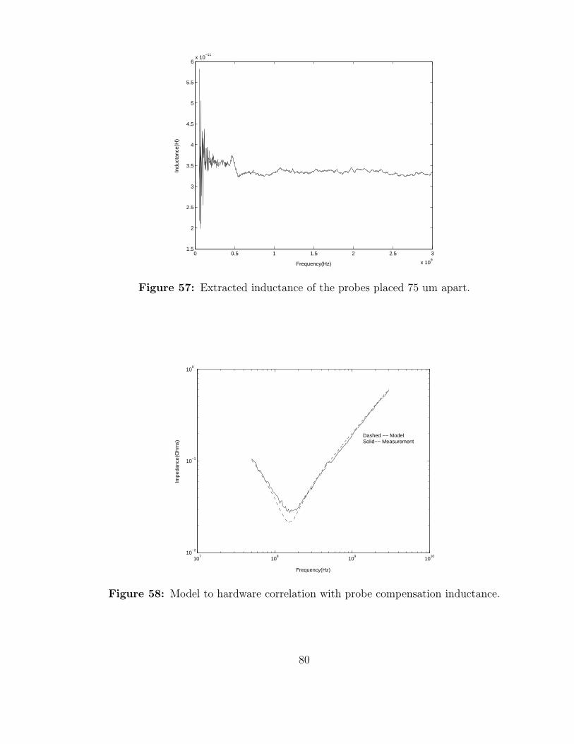
0 0.5 1 1.5 2 2.5 3
x 109
1.5
2
2.5
3
3.5
4
4.5
5
5.5
6x 10
−11
Frequency(Hz)
Indu
ctan
ce(H
)
Figure 57: Extracted inductance of the probes placed 75 um apart.
107
108
109
1010
10−2
10−1
100
Frequency(Hz)
Impe
danc
e(O
hms)
Dashed −− Model Solid−− Measurement
Figure 58: Model to hardware correlation with probe compensation inductance.
80

0.5 1 1.5 2 2.5 3 3.5 4
x 108
0
1
2
3
4
5
6
7
8
9
x 10−8
Frequency(Hz)
Cap
acita
nce(
F)
Figure 59: Extracted capacitance of the 2.1 mm diameter capacitor.
107
108
109
1010
10−2
10−1
100
0.9mm side square1mm side square2.1mm diameter circle
Figure 60: Comparison of measured hydrothermal capacitors of different sizes.
81

3.4 Summary
The measurement and modeling methodology used to characterize parallel plate struc-
tures was presented in this chapter. The measurement methodology included self and
transfer impedance measurements. Equations were derived for both cases that ac-
counted for the error introduced because of any discontinuities in the measurement
set up and quantified the error terms. It was concluded that for low impedance struc-
tures the error introduced by any discontinuity could be neglected if the two port
measurement methodology was used. The frequency dependent capacitance, induc-
tance, and resistance were extracted from the measurements. Models were developed
for these capacitors using the transmission matrix method. Model to measurement
correlation was shown for different capacitors by accounting for the parasitic induc-
tances introduced by the probes.
82
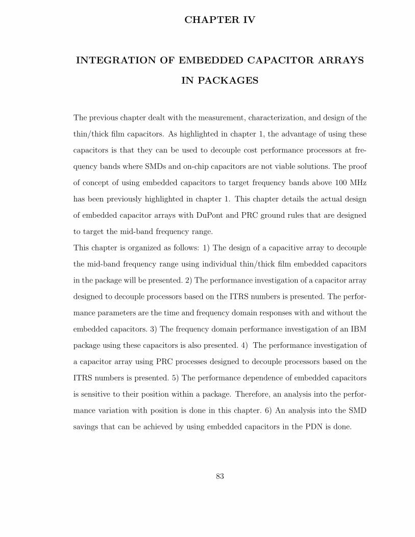
CHAPTER IV
INTEGRATION OF EMBEDDED CAPACITOR ARRAYS
IN PACKAGES
The previous chapter dealt with the measurement, characterization, and design of the
thin/thick film capacitors. As highlighted in chapter 1, the advantage of using these
capacitors is that they can be used to decouple cost performance processors at fre-
quency bands where SMDs and on-chip capacitors are not viable solutions. The proof
of concept of using embedded capacitors to target frequency bands above 100 MHz
has been previously highlighted in chapter 1. This chapter details the actual design
of embedded capacitor arrays with DuPont and PRC ground rules that are designed
to target the mid-band frequency range.
This chapter is organized as follows: 1) The design of a capacitive array to decouple
the mid-band frequency range using individual thin/thick film embedded capacitors
in the package will be presented. 2) The performance investigation of a capacitor array
designed to decouple processors based on the ITRS numbers is presented. The perfor-
mance parameters are the time and frequency domain responses with and without the
embedded capacitors. 3) The frequency domain performance investigation of an IBM
package using these capacitors is also presented. 4) The performance investigation of
a capacitor array using PRC processes designed to decouple processors based on the
ITRS numbers is presented. 5) The performance dependence of embedded capacitors
is sensitive to their position within a package. Therefore, an analysis into the perfor-
mance variation with position is done in this chapter. 6) An analysis into the SMD
savings that can be achieved by using embedded capacitors in the PDN is done.
83

The concept of individual thin/thick film embedded capacitor arrays in the pack-
age was presented in chapter 3. The capacitor array is designed to meet a certain
target impedance over a frequency band above 100 MHz. The number of capacitors
required of each type is given by equation 64 and has been rewritten here.
Numberofcapacitors =Ztarget
ESRcap(64)
As mentioned in chapter 3, the embedded capacitors should be placed directly under
the die shadow and the vias connecting the capacitors to the processor should connect
to the solder bumps of the processor. The frequency band over which decoupling can
be provided depends on the capacitor technology and ground rules, however the rules
used in the design of the array is transparent over any technology. The DuPont and
PRC technologies introduced in chapter 3 are used in this section to design capacitor
arrays to decouple frequencies above 100 MHz.
4.1 Design of a capacitive array using Dupont materialsand process ground rules for a 65 nm ITRS cost per-
formance processor.
The previous chapter dealt with the modeling, measurement, and characterization
of embedded capacitors. The use of these capacitors in decoupling cost performance
type applications in the mid-band frequency will be described here. As mentioned
before, the mid-band frequency is defined as the frequency range between 100 MHz
to 2 GHz. Therefore, the package structures that were modeled for each technology
will be described in detail here.
The cross section of the proposed package is shown in Fig. 61. The package
consists of a core of thickness 0.6 mm shown in Fig. 62. The core is split into seven
constituents as shown in Fig. 62. The total thickness of the structure excluding the
metal levels in this case is 600 um.
The build up layers are added to the core in Fig. 62 to obtain the complete package
84
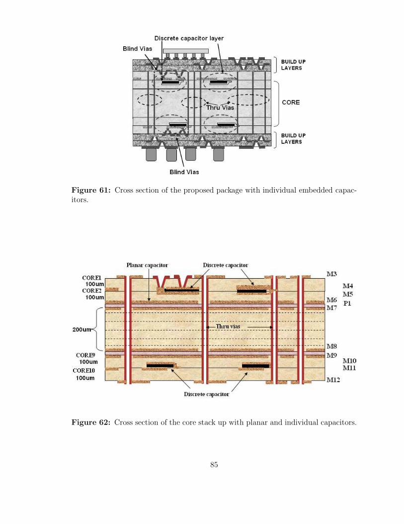
Figure 61: Cross section of the proposed package with individual embedded capac-itors.
Figure 62: Cross section of the core stack up with planar and individual capacitors.
85
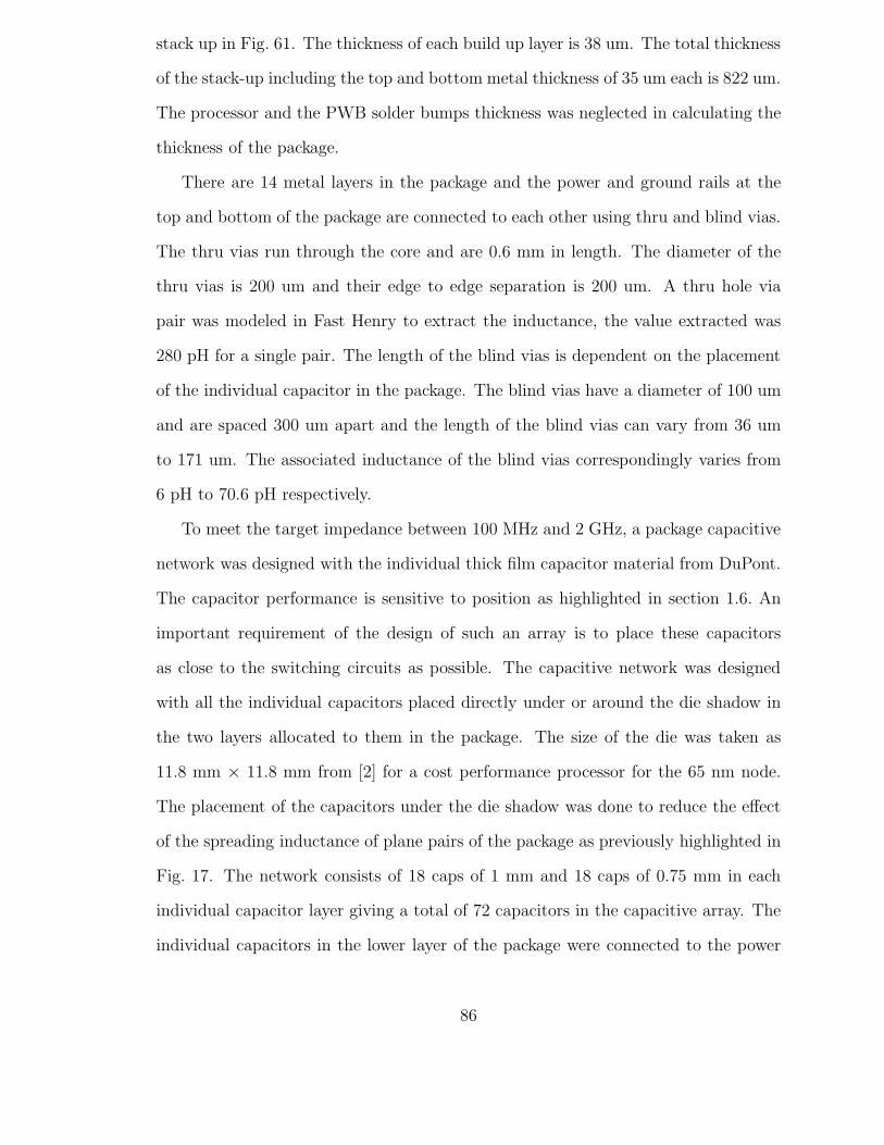
stack up in Fig. 61. The thickness of each build up layer is 38 um. The total thickness
of the stack-up including the top and bottom metal thickness of 35 um each is 822 um.
The processor and the PWB solder bumps thickness was neglected in calculating the
thickness of the package.
There are 14 metal layers in the package and the power and ground rails at the
top and bottom of the package are connected to each other using thru and blind vias.
The thru vias run through the core and are 0.6 mm in length. The diameter of the
thru vias is 200 um and their edge to edge separation is 200 um. A thru hole via
pair was modeled in Fast Henry to extract the inductance, the value extracted was
280 pH for a single pair. The length of the blind vias is dependent on the placement
of the individual capacitor in the package. The blind vias have a diameter of 100 um
and are spaced 300 um apart and the length of the blind vias can vary from 36 um
to 171 um. The associated inductance of the blind vias correspondingly varies from
6 pH to 70.6 pH respectively.
To meet the target impedance between 100 MHz and 2 GHz, a package capacitive
network was designed with the individual thick film capacitor material from DuPont.
The capacitor performance is sensitive to position as highlighted in section 1.6. An
important requirement of the design of such an array is to place these capacitors
as close to the switching circuits as possible. The capacitive network was designed
with all the individual capacitors placed directly under or around the die shadow in
the two layers allocated to them in the package. The size of the die was taken as
11.8 mm × 11.8 mm from [2] for a cost performance processor for the 65 nm node.
The placement of the capacitors under the die shadow was done to reduce the effect
of the spreading inductance of plane pairs of the package as previously highlighted in
Fig. 17. The network consists of 18 caps of 1 mm and 18 caps of 0.75 mm in each
individual capacitor layer giving a total of 72 capacitors in the capacitive array. The
individual capacitors in the lower layer of the package were connected to the power
86

Figure 63: Layout of a individual capacitor layer in the package.
and ground bumps of the processor via blind and thru vias as mentioned earlier in this
section. The layout of one of the layers of individual embedded capacitors is shown in
Fig. 63. The network is designed such that majority of the vias from the capacitors
connect directly to the flip chip solder bumps of the processor. The design ground
rules prevent thru vias to be spread uniformly across the die shadow as seen by the
non-uniformity of the position of the thru vias in Fig. 63. Process ground rules specific
to DuPont capacitor materials were used to design the embedded capacitor layout.
A ground rules that were used will be briefly mentioned in this part of the section.
Fig. 64 captures a few of the design ground rules for the capacitor network layout. The
minimum and maximum size of the electrodes as mentioned before are 0.5 mm and
3 mm a side respectively. The size of a dielectric is 0.625 mm larger than the size of the
electrode on each side, therefore the area occupied by the structure is larger than that
occupied by the effective capacitor. If there are no thru holes between a capacitor,
the distance between dielectrics is 0.625 mm. The spacing between the dielectrics
with thru holes between them is 1.05 mm. The process ground rules are listed in
table 7. The embedded capacitor network was designed to target the frequency band
between 100 MHz and 2 GHz as shown in Fig. 65. To provide decoupling from DC to
multiples of chip operating frequencies VRMs, SMDs, and on-chip capacitance would
87

Figure 64: The design ground rules for the capacitor network in the package.
Table 7: DuPont process ground rulesParameters Value
Maximum size of a capacitor electrode 120 milsMinimum size of a capacitor electrode 20 mils
Dielectric constant 3000Loss tangent 0.05 @ 1 MHz
Thickness of top and bottom electrode 3 − 5 um (0.12-0.3) milsSpacing between two capacitors Function of their sizesThe minimum thru via diameter 15 mils
Via clearance diameter Via diameter + 15 milsThe spacing between the vias 30 mils
Dielectric size Electrode size + 20 mils (10 mils / side)Dielectric thickness 20 ± 3 microns fired
88
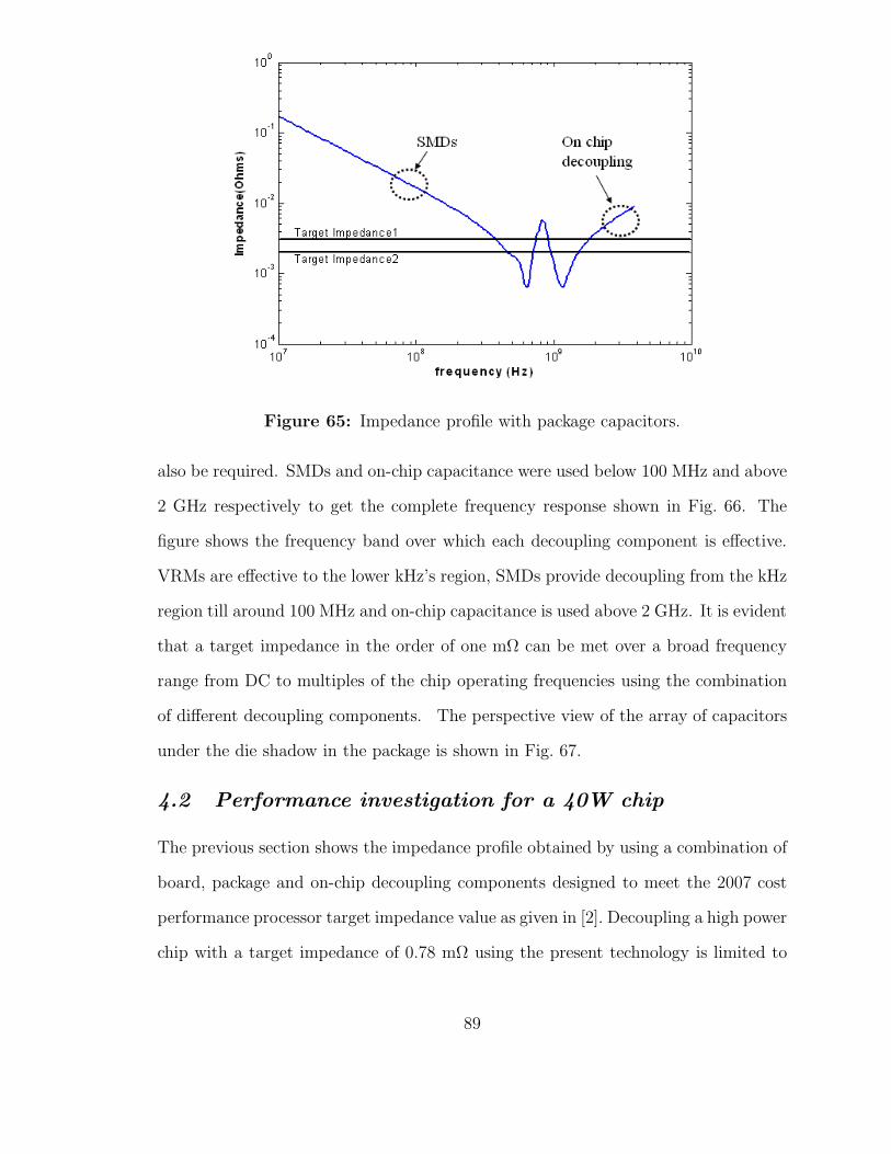
Figure 65: Impedance profile with package capacitors.
also be required. SMDs and on-chip capacitance were used below 100 MHz and above
2 GHz respectively to get the complete frequency response shown in Fig. 66. The
figure shows the frequency band over which each decoupling component is effective.
VRMs are effective to the lower kHz’s region, SMDs provide decoupling from the kHz
region till around 100 MHz and on-chip capacitance is used above 2 GHz. It is evident
that a target impedance in the order of one mΩ can be met over a broad frequency
range from DC to multiples of the chip operating frequencies using the combination
of different decoupling components. The perspective view of the array of capacitors
under the die shadow in the package is shown in Fig. 67.
4.2 Performance investigation for a 40W chip
The previous section shows the impedance profile obtained by using a combination of
board, package and on-chip decoupling components designed to meet the 2007 cost
performance processor target impedance value as given in [2]. Decoupling a high power
chip with a target impedance of 0.78 mΩ using the present technology is limited to
89
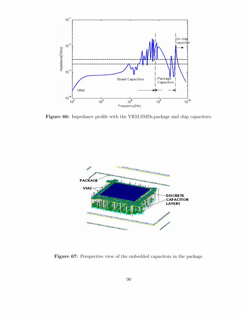
Figure 66: Impedance profile with the VRM,SMDs,package and chip capacitors.
Figure 67: Perspective view of the embedded capacitors in the package.
90

a very narrow frequency band at 600 MHz and 1 GHz. Therefore, this section looks
at alternatives where the capacitive network is used to decouple a lower power chip
over a broader frequency range.
4.2.1 Time domain performance of the capacitive array
The time domain performance of the capacitive array targeting a lower power chip
is investigated in this section. The simulations were carried out to capture the per-
formance with a 2 GHz clock as the input to the system. The rise time and fall
time of the current pulse is 50 psec respectively and the time period of the clock is
500 psec as shown in Fig. 68. The target impedance to be met decides the magni-
tude of the current pulse. In this simulation, a 40 W chip was considered and a core
voltage of 1 V was assumed. Therefore from (2), the magnitude of the current pulse
calculated assuming a core voltage of 1 V is 40 A. The target impedance from 1 is
2.5 mΩ. To get the time domain response of the system, the fourier transform of the
input current pulse train is multiplied with the frequency domain data of the PDN.
The inverse fourier transform of the resultant is then taken to get the time domain
response. The system simulation was initially carried out with a VRM, SMDs and
on-chip decoupling capacitors. 25 nF of on-chip decoupling capacitance was consid-
ered in the simulation. The time domain performance of the system is shown in Fig.
69. Switching noise of the order of 400 mV peak to peak is observed from the fig-
ure. To highlight the improvement with embedded package capacitors, the system
was simulated with the VRM, SMDs, package and on-chip capacitors. The switching
noise observed in this case is 80 mV peak to peak and is shown in Fig. 70. A five time
improvement in the switching noise performance is clearly seen with the inclusion of
embedded capacitors in the package for a 40 W chip.
From the frequency domain response of the capacitive array, it can be concluded
that a 40 W chip can be decoupled in the frequency range from 350 MHz to 2 GHz.
91
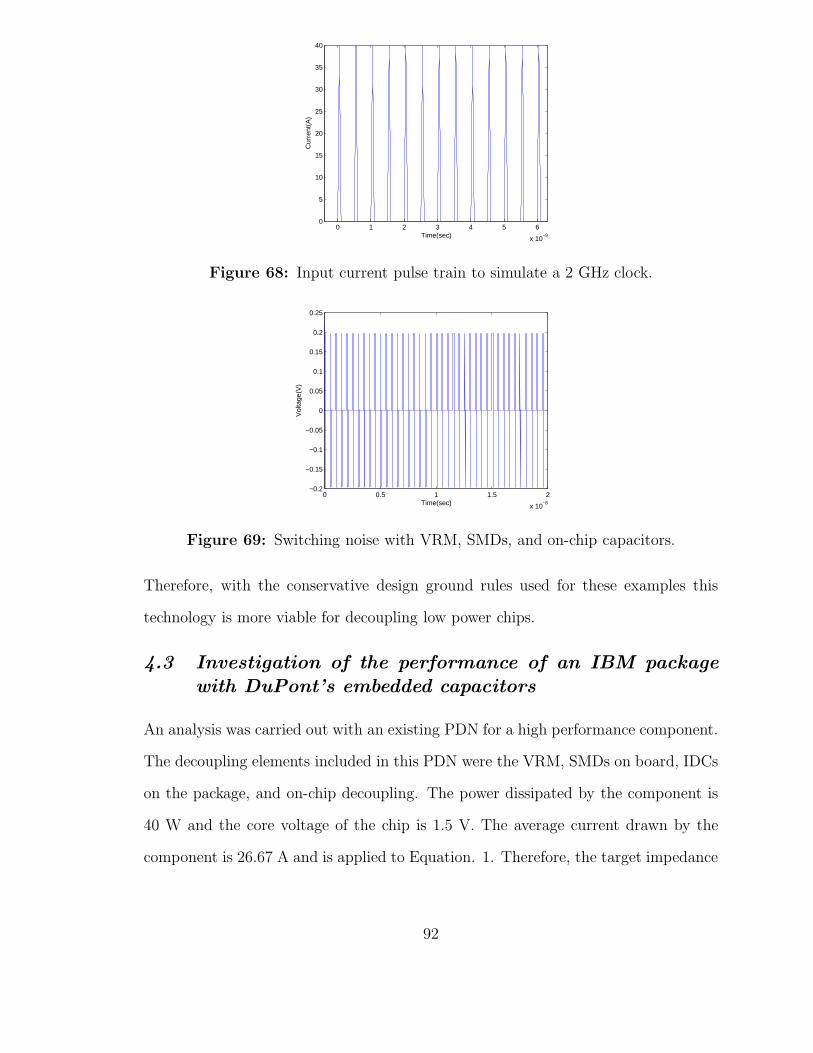
0 1 2 3 4 5 6
x 10−9
0
5
10
15
20
25
30
35
40
Time(sec)
Cur
rent
(A)
Figure 68: Input current pulse train to simulate a 2 GHz clock.
0 0.5 1 1.5 2
x 10−8
−0.2
−0.15
−0.1
−0.05
0
0.05
0.1
0.15
0.2
0.25
Time(sec)
Vol
tage
(V)
Figure 69: Switching noise with VRM, SMDs, and on-chip capacitors.
Therefore, with the conservative design ground rules used for these examples this
technology is more viable for decoupling low power chips.
4.3 Investigation of the performance of an IBM packagewith DuPont’s embedded capacitors
An analysis was carried out with an existing PDN for a high performance component.
The decoupling elements included in this PDN were the VRM, SMDs on board, IDCs
on the package, and on-chip decoupling. The power dissipated by the component is
40 W and the core voltage of the chip is 1.5 V. The average current drawn by the
component is 26.67 A and is applied to Equation. 1. Therefore, the target impedance
92

0 0.5 1 1.5 2
x 10−8
−0.04
−0.03
−0.02
−0.01
0
0.01
0.02
0.03
0.04
Time(sec)
Vol
tage
(V)
Figure 70: Switching noise with VRM, SMDs, on chip and embedded packagecapacitors.
that has to be met is 5.6 mΩ. Fig. 71 shows the cross section of the package under
consideration. It has a 4 − 2 − 4 laminate stack up and has multiple voltage and
ground planes.
The distribution of the power-ground planes is shown in Fig. 72. The layout show-
ing the IDCs on the package and the different voltage planes for the MEM(Memory),
Core and I/Os is shown Fig. 78. The frequency domain response was obtained by
modeling the package with the different decoupling components using the Transmis-
sion Matrix Method [31]. Ten 1206 SMDs were connected to the printed circuit
board. The value of the SMD capacitors are C = 22 uF, ESR = 8 mΩ and ESL =
1 nH. Nine IDCs were connected to the package. The value of the IDCs are C =
100 nF, ESR = 8 mΩ and ESL = 90 pH. 400 nF of on-chip decoupling was used in
the analysis. Fig. 74 shows the response of the PDN with the above mentioned decou-
pling elements. The parasitic mounting inductance of the capacitors was included in
the simulations. The target impedance of 5.6 mΩ is met over a broad range by using
the above mentioned decoupling elements except for two parallel resonance peaks as
observed in Fig. 74. The first parallel resonance is between the PCB SMDs and the
IDC capacitors and the second resonance is due to the IDCs and on-chip capacitance.
The target impedance is not met in the frequency bands from 5 MHz to 25 MHz
93
Figure 71: Cross section of the IBM package.
Figure 72: Power planes of the IBM package.
94

Figure 73: IBM package layout showing the IDCs and voltage planes for core,MEM,and I/O.
Figure 74: Impedance profile with SMDs and on-chip decoupling capacitor.
95

and from 60 MHz to 120 MHz respectively because of these resonances. The focus
of this analysis is on the use of package embedded capacitors to target the frequency
band in the range of 100 MHz and above. Therefore, the following analysis is done to
target the second parallel resonance between the IDCs and on-chip capacitance. The
first resonance could be reduced by proper selection of SMDs. Meeting the target
impedance for higher power components would be an issue with the traditional de-
coupling elements. To illustrate the problem, if high density components in the order
of 50 W,70 W, and 100 W were to be decoupled by the same elements then the target
impedance numbers that have to be met for a core voltage of 1.5 V in each case are
4.5 mΩ, 3.2 mΩ and 2.25 mΩ respectively. These target impedances are shown in
Fig. 74. It can be observed that frequency band over which the target impedance can
be met with the above mentioned decoupling elements is restricted to smaller bands
for higher power components. To target the frequency band from 60 MHz to 120 MHz
shown in the circled area in Fig. 74, embedded package capacitors can be used. To
target the desired frequency band in this case, two capacitors with 25 mm2 area were
placed in layers two and five each with different number of via connections to target
different frequency bands in the 60 MHz to 120 MHz range. The loop inductance
of power/ground (P/G) C4 solder ball of diameter 150 um and pitch 225 um along
with a pair of P/G vias from the C4 layer to the core voltage level in layer three is
computed as 43 pH using FastHenry [30]. Similarly, the loop inductance of a similar
structure from the C4 layer to layer five is 70 pH. The frequency response of the PDN
with the embedded capacitor in the package is shown in Fig. 75 and the impedance
in the frequency band from 60 MHz to 120 MHz is met.
4.3.1 I/O Decoupling Analysis
This section focuses on the use of embedded capacitors in decoupling I/Os. Two
different single ended I/O configurations are analyzed in this section. The two I/O
96
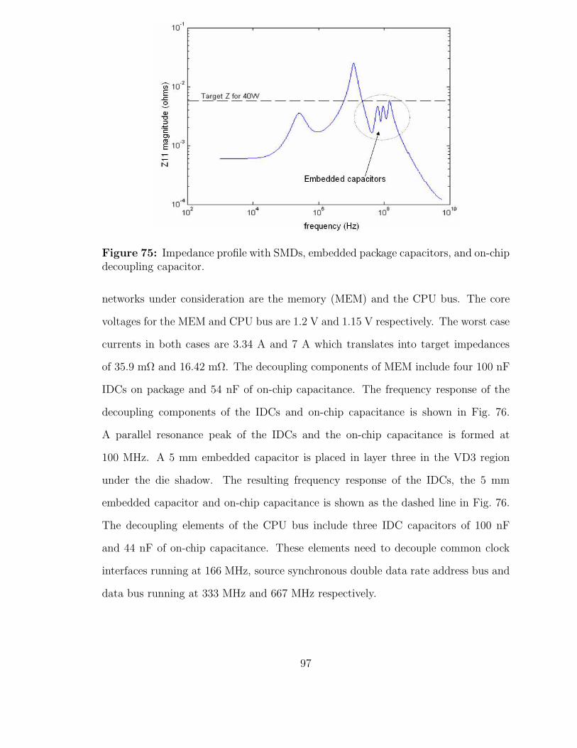
Figure 75: Impedance profile with SMDs, embedded package capacitors, and on-chipdecoupling capacitor.
networks under consideration are the memory (MEM) and the CPU bus. The core
voltages for the MEM and CPU bus are 1.2 V and 1.15 V respectively. The worst case
currents in both cases are 3.34 A and 7 A which translates into target impedances
of 35.9 mΩ and 16.42 mΩ. The decoupling components of MEM include four 100 nF
IDCs on package and 54 nF of on-chip capacitance. The frequency response of the
decoupling components of the IDCs and on-chip capacitance is shown in Fig. 76.
A parallel resonance peak of the IDCs and the on-chip capacitance is formed at
100 MHz. A 5 mm embedded capacitor is placed in layer three in the VD3 region
under the die shadow. The resulting frequency response of the IDCs, the 5 mm
embedded capacitor and on-chip capacitance is shown as the dashed line in Fig. 76.
The decoupling elements of the CPU bus include three IDC capacitors of 100 nF
and 44 nF of on-chip capacitance. These elements need to decouple common clock
interfaces running at 166 MHz, source synchronous double data rate address bus and
data bus running at 333 MHz and 667 MHz respectively.
97
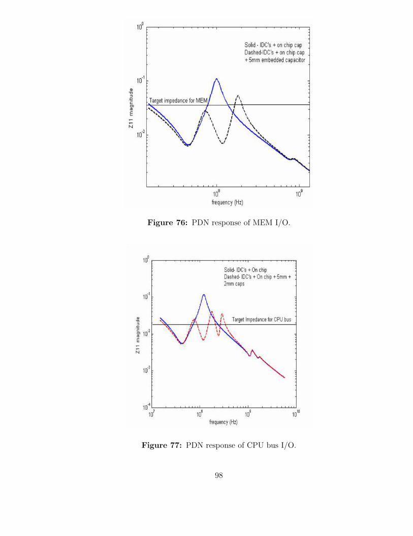
Figure 76: PDN response of MEM I/O.
Figure 77: PDN response of CPU bus I/O.
98
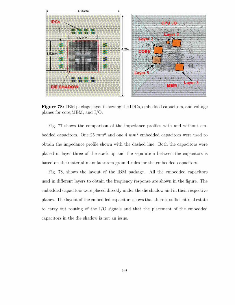
Figure 78: IBM package layout showing the IDCs, embedded capacitors, and voltageplanes for core,MEM, and I/O.
Fig. 77 shows the comparison of the impedance profiles with and without em-
bedded capacitors. One 25 mm2 and one 4 mm2 embedded capacitors were used to
obtain the impedance profile shown with the dashed line. Both the capacitors were
placed in layer three of the stack up and the separation between the capacitors is
based on the material manufacturers ground rules for the embedded capacitors.
Fig. 78, shows the layout of the IBM package. All the embedded capacitors
used in different layers to obtain the frequency response are shown in the figure. The
embedded capacitors were placed directly under the die shadow and in their respective
planes. The layout of the embedded capacitors shows that there is sufficient real estate
to carry out routing of the I/O signals and that the placement of the embedded
capacitors in the die shadow is not an issue.
99

4.3.2 On-chip capacitance for decoupling high performance components
- This section focuses on the effect of on-chip capacitance to decouple high perfor-
mance components. The results of decoupling PDNs with various decoupling com-
ponents have been shown in the previous sections. In this section it is shown that
an increase in the amount of on-chip decoupling capacitance can replace some of
the higher frequency decoupling components. In the previous analysis the amount
of on-chip capacitance for decoupling the core was assumed to be 400 nF. Fig. 79
shows the analysis results for core decoupling using fixed number of SMDs and IDCs
but with different values of on-chip capacitance values. It is observed that the use
of higher frequency decoupling components can be reduced with an increase in the
on-chip capacitance. A drawback of such an approach is that the amount of real
estate and additional process steps that the on-chip capacitance requires. The trade-
off of increasing the on-chip capacitance could be a decrease in the logic density or
additional manufacturing technology investments. Therefore, an alternate approach
could be to provide most of the high frequency decoupling from embedded package
capacitors as shown in [63],[62]. The advantage would be an increase in the amount
of real estate for logic on-chip and increase in the capacitance that can be provided
for decoupling from the package. Resistance of on-chip decoupling capacitors is the
major drawback in decoupling I/O circuits. This can be overcome by the use of less
resistive package embedded capacitors. Other advantages of using package capaci-
tors for I/O decoupling could be an increase in the real estate for circuitry on chip.
The major contributors to I/O noise are the SSN that can couple from one driver to
another and crosstalk between traces. A reduction in the switching noise due to the
embedded capacitors can be used as an incentive to place the traces on the package
closer to each other as the noise budget for cross talk is increased. This translates to
reduction in the number of wiring layers and an overall reduction in the size and cost
of the package [64]. It is noted that with the knowledge of the current pulse signature
100

Figure 79: Frequency response of the core PDN with different values of on-chipcapacitance .
of the component, time domain analysis can be done which could help in obtaining a
more optimum design of the PDN as shown in [65].
4.4 Design of capacitive array for decoupling using the hy-
drothermal capacitor material and Packaging ResearchCenter (PRC) process ground rules
The previous sections of this chapter highlighted the performance improvements in
decoupling above 100 MHz by using the DuPont capacitors and ground rules for de-
signing a package with these capacitors. This section investigates the performance
improvements by using hydrothermal capacitors fabricated at the PRC. The package
for the hydrothermal capacitors is different in structure as compared to the DuPont
ground rules. The structure is shown in Fig. 80. The capacitors are placed at the
two bottom most layers, the rest of the layers are built up after the capacitor layers
are tested. The package dimensions are based on the packaging research center(PRC)
ground rules. The ground rules that were used to propose the package are listed
in table 8. The methodology used to design the capacitive array in the package
101

Figure 80: Stack up of the package with hydrothermal capacitors.
Table 8: Packaging Research Center(PRC) ground rulesParameters Value
Power ground plane dielectric thickness 9 umPower ground plane dielectric constant 2.65
Loss tangent 0.008Line and space 10 umVia diameter 20 umVia pad size 40 umVia pitch 60 um
Capacitor minimum size 300 um sideCapacitor maximum size 3000 um side
Spacing between capacitors 100 um
102
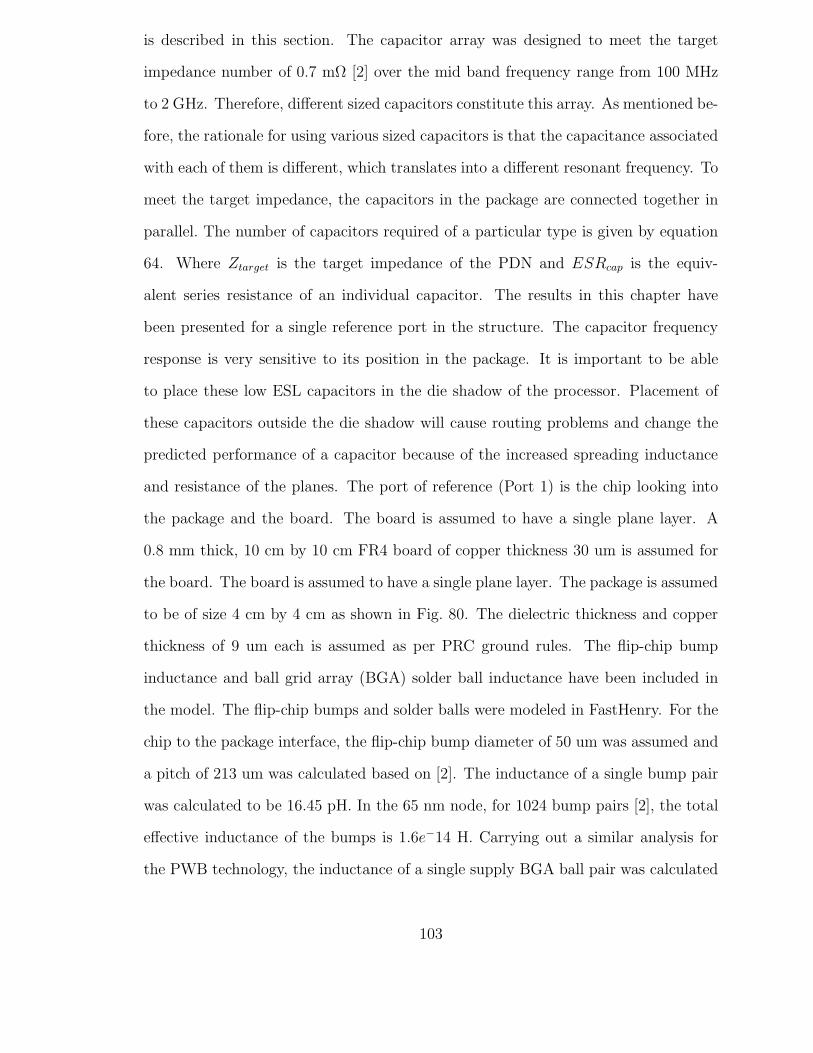
is described in this section. The capacitor array was designed to meet the target
impedance number of 0.7 mΩ [2] over the mid band frequency range from 100 MHz
to 2 GHz. Therefore, different sized capacitors constitute this array. As mentioned be-
fore, the rationale for using various sized capacitors is that the capacitance associated
with each of them is different, which translates into a different resonant frequency. To
meet the target impedance, the capacitors in the package are connected together in
parallel. The number of capacitors required of a particular type is given by equation
64. Where Ztarget is the target impedance of the PDN and ESRcap is the equiv-
alent series resistance of an individual capacitor. The results in this chapter have
been presented for a single reference port in the structure. The capacitor frequency
response is very sensitive to its position in the package. It is important to be able
to place these low ESL capacitors in the die shadow of the processor. Placement of
these capacitors outside the die shadow will cause routing problems and change the
predicted performance of a capacitor because of the increased spreading inductance
and resistance of the planes. The port of reference (Port 1) is the chip looking into
the package and the board. The board is assumed to have a single plane layer. A
0.8 mm thick, 10 cm by 10 cm FR4 board of copper thickness 30 um is assumed for
the board. The board is assumed to have a single plane layer. The package is assumed
to be of size 4 cm by 4 cm as shown in Fig. 80. The dielectric thickness and copper
thickness of 9 um each is assumed as per PRC ground rules. The flip-chip bump
inductance and ball grid array (BGA) solder ball inductance have been included in
the model. The flip-chip bumps and solder balls were modeled in FastHenry. For the
chip to the package interface, the flip-chip bump diameter of 50 um was assumed and
a pitch of 213 um was calculated based on [2]. The inductance of a single bump pair
was calculated to be 16.45 pH. In the 65 nm node, for 1024 bump pairs [2], the total
effective inductance of the bumps is 1.6e−14 H. Carrying out a similar analysis for
the PWB technology, the inductance of a single supply BGA ball pair was calculated
103
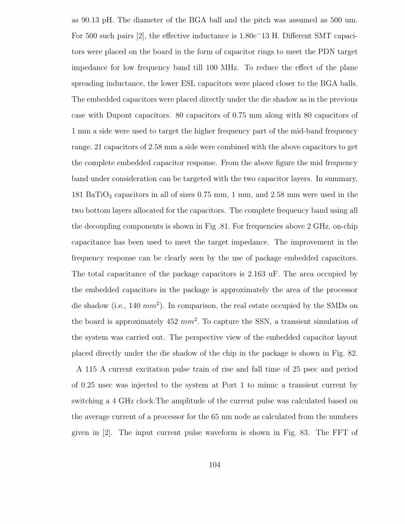
as 90.13 pH. The diameter of the BGA ball and the pitch was assumed as 500 um.
For 500 such pairs [2], the effective inductance is 1.80e−13 H. Different SMT capaci-
tors were placed on the board in the form of capacitor rings to meet the PDN target
impedance for low frequency band till 100 MHz. To reduce the effect of the plane
spreading inductance, the lower ESL capacitors were placed closer to the BGA balls.
The embedded capacitors were placed directly under the die shadow as in the previous
case with Dupont capacitors. 80 capacitors of 0.75 mm along with 80 capacitors of
1 mm a side were used to target the higher frequency part of the mid-band frequency
range. 21 capacitors of 2.58 mm a side were combined with the above capacitors to get
the complete embedded capacitor response. From the above figure the mid frequency
band under consideration can be targeted with the two capacitor layers. In summary,
181 BaTiO3 capacitors in all of sizes 0.75 mm, 1 mm, and 2.58 mm were used in the
two bottom layers allocated for the capacitors. The complete frequency band using all
the decoupling components is shown in Fig .81. For frequencies above 2 GHz, on-chip
capacitance has been used to meet the target impedance. The improvement in the
frequency response can be clearly seen by the use of package embedded capacitors.
The total capacitance of the package capacitors is 2.163 uF. The area occupied by
the embedded capacitors in the package is approximately the area of the processor
die shadow (i.e., 140 mm2). In comparison, the real estate occupied by the SMDs on
the board is approximately 452 mm2. To capture the SSN, a transient simulation of
the system was carried out. The perspective view of the embedded capacitor layout
placed directly under the die shadow of the chip in the package is shown in Fig. 82.
A 115 A current excitation pulse train of rise and fall time of 25 psec and period
of 0.25 nsec was injected to the system at Port 1 to mimic a transient current by
switching a 4 GHz clock.The amplitude of the current pulse was calculated based on
the average current of a processor for the 65 nm node as calculated from the numbers
given in [2]. The input current pulse waveform is shown in Fig. 83. The FFT of
104

Figure 81: Complete frequency band with hydrothermal capacitors and all thedecoupling components.
Figure 82: Perspective view of the PRC package with hydrothermal embeddedcapacitors.
105
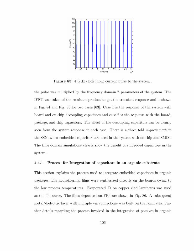
Figure 83: 4 GHz clock input current pulse to the system .
the pulse was multiplied by the frequency domain Z parameters of the system. The
IFFT was taken of the resultant product to get the transient response and is shown
in Fig. 84 and Fig. 85 for two cases [63]. Case 1 is the response of the system with
board and on-chip decoupling capacitors and case 2 is the response with the board,
package, and chip capacitors. The effect of the decoupling capacitors can be clearly
seen from the system response in each case. There is a three fold improvement in
the SSN, when embedded capacitors are used in the system with on-chip and SMDs.
The time domain simulations clearly show the benefit of embedded capacitors in the
system.
4.4.1 Process for Integration of capacitors in an organic substrate
This section explains the process used to integrate embedded capacitors in organic
packages. The hydrothermal films were synthesized directly on the boards owing to
the low process temperatures. Evaporated Ti on copper clad laminates was used
as the Ti source. The films deposited on FR4 are shown in Fig. 86. A subsequent
metal/dielectric layer with multiple via connections was built on the laminates. Fur-
ther details regarding the process involved in the integration of passives in organic
106
Figure 84: SSN magnitude with VRM, SMDs and on-chip capacitance.
Figure 85: SSN magnitude with VRM, SMDs ,embedded capacitors and on-chipcapacitance.
substrates can be found in [66] and has not been mentioned in this thesis. A picture
of a combination of assembled capacitors is shown in Fig. 87.
107

Figure 86: Integration process of hydrothermal capacitors in an organic package.
4.5 Frequency performance dependence on location
A series of simulations were carried out to highlight the performance variation of em-
bedded capacitors with change in position within the package. The Dupont process
ground rules were used to carry out the analysis. The simulations were done to high-
light two important position variations. An array of four 2mm × 2mm capacitors was
used to highlight the concept instead of the whole decoupling array. The parameters
of a single 2mm × 2mm capacitor is as follows- C = 5.31 nF, ESR = 8.59 mΩ and
ESL =17.24 pH + the inductance of the vias, where 17.24 pH is the equivalent series
inductance of the capacitor. In caseA as shown in Fig. 88, the capacitor location
was changed vertically in the package. In case B, the capacitor location was changed
horizontally with respect to the processor as shown in Fig. 90.
108
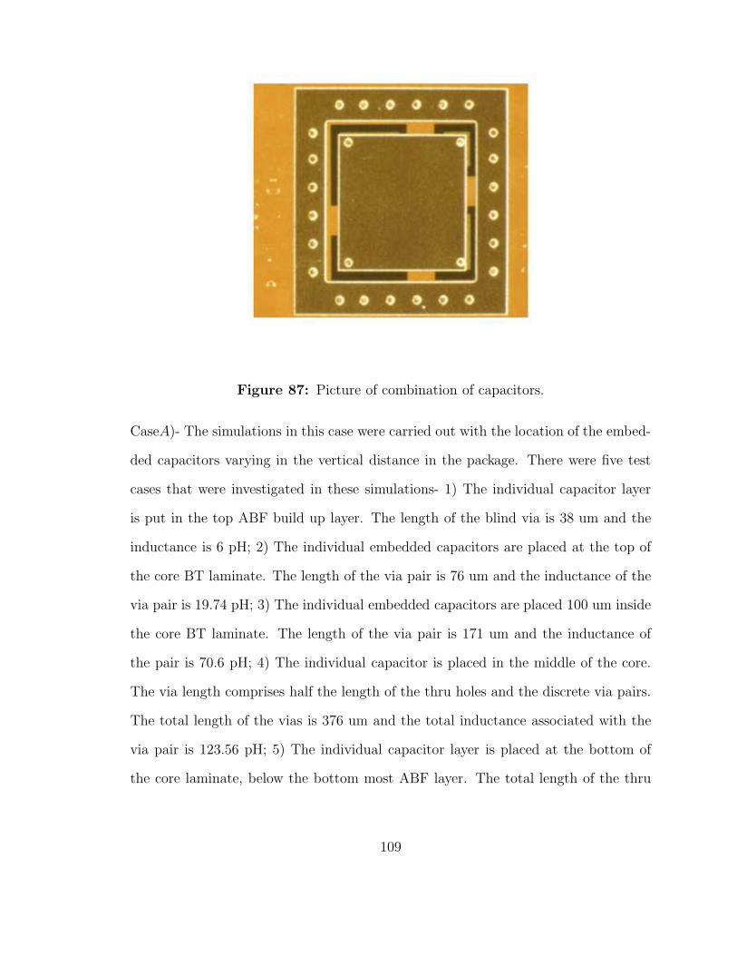
Figure 87: Picture of combination of capacitors.
CaseA)- The simulations in this case were carried out with the location of the embed-
ded capacitors varying in the vertical distance in the package. There were five test
cases that were investigated in these simulations- 1) The individual capacitor layer
is put in the top ABF build up layer. The length of the blind via is 38 um and the
inductance is 6 pH; 2) The individual embedded capacitors are placed at the top of
the core BT laminate. The length of the via pair is 76 um and the inductance of the
via pair is 19.74 pH; 3) The individual embedded capacitors are placed 100 um inside
the core BT laminate. The length of the via pair is 171 um and the inductance of
the pair is 70.6 pH; 4) The individual capacitor is placed in the middle of the core.
The via length comprises half the length of the thru holes and the discrete via pairs.
The total length of the vias is 376 um and the total inductance associated with the
via pair is 123.56 pH; 5) The individual capacitor layer is placed at the bottom of
the core laminate, below the bottom most ABF layer. The total length of the thru
109

Table 9: Via length and inductance values for different casesCase Via length(um) Via inductance(pH)
1 38 62 76 19.743 171 70.64 376 123.565 752 319.48
Figure 88: Different vertical locations of the embedded capacitor in the package.
hole and discrete via pair is 752 um and the associated inductance of the via pair
is 319.48 pH. The via length and inductance values have been summarized for the
different cases in table 9.
The change in array performance is evident from Fig. 89. The shift in the resonant
frequency to the lower frequency band can be attributed to the increase in the via
inductance in each corresponding case. The minimum series resistance of the array
remains almost constant because of the negligible resistance of the vias. These results
can be translated into the design of a capacitive array such that the capacitors that
are required to target the lower frequency band are placed vertically farther away
from the active circuit than the capacitors that decouple higher frequency ranges.
CaseB) This case analyzes the variation of the four 2 mm × 2 mm capacitor
array performance with a change in the horizontal placement as shown in Fig. 90. It
had been mentioned previously that all the embedded capacitors were placed close
to or slightly around the processor. Fig. 91, shows the performance change with
the horizontal variation of the capacitor array position. The vertical distance of
110

107
108
109
1010
10−3
10−2
10−1
100
101
Frequency (Hz)
Impe
danc
e(O
hms)
Case1
Case2
Case3
Case4
Case5
The ESR is almost constant as the via resistance is negligible
Decreasing bandwidth
Figure 89: Variation of capacitor array performance with vertical distance.
Figure 90: Horizontal variation of the embedded capacitor in the package.
111

107
108
109
1010
10−3
10−2
10−1
100
101
Frequency (Hz)
Impe
danc
e(oh
ms)
Case3
Case4
Case 2 Case 1
Case5
Increasing targetimpedance
Decreasing bandwidth
Figure 91: Variation of capacitor array performance with horizontal distance.
the capacitors is kept constant in all the simulation scenarios for this case. The
inductance of the a via pair was taken as 19.74 pH. Two via pairs were considered
for each capacitor in the array.
Five test cases were investigated 1) The capacitor array was placed directly under
the processor. 2) The array was placed 2 mm away from the processor. 3) The array
was placed 4 mm away from the processor. 4) The array was placed 1.2 cm away.
5) The placement of the array was 1.9 cm away from the processor. The reduction
in the resonant frequency of the capacitor array is because of the increased effect
of the spreading inductance of the planes as they are placed further away from the
processor. An increase in the distance of the capacitor array from the processor also
leads to the increased effect of the resistance of the planes. The effect can be seen
in the variation of the minimum series resistance of the array, which increases from
one through five. Therefore, from the above analysis it is evident that stacking the
capacitors vertically would be advantageous if the PDN is required to decouple active
high current densities circuits with very low target impedances.
112

4.5.1 SMD savings using Embedded Capacitors
SMD savings with the introduction of embedded capacitors in the PDN is highlighted
in this section. It has been shown in section 1.6 that SMDs reach their decoupling lim-
itation close to 100 MHz, therefore this frequency point has been chosen for carrying
out the following analysis.
The steps involved in determining the number of SMDs that can be saved are
determined as follows- Step 1 Use only SMDs in the PDN to meet a target impedance
till 100MHz. Step 2 Design the PDN by using embedded capacitors to meet the
same target impedance and then introduce SMDs to meet the target impedance at
100 MHz. Observe if there any savings in the SMDs in step 2 as compared to step 1.
The analysis was carried out with Dupont capacitor and process ground rules.
In the simulations, it is assumed that the SMDs are connected directly to the
PWB solder balls. The dimensions and the pitch of the solder ball are assumed
to be 500 um each. A pair of the solder balls were modeled in Fast Henry and the
associated inductance of a single pair was calculated to be 138.22 pH. The SMDs under
consideration are the low inductance capacitors that are available from AVX [67]. The
lead inductance of the AVX LICA capacitors is 25 pH and that of a single thru hole via
pair is 280 pH. 100 via pairs are assumed within the package, therefore the effective
inductance of the thru vias is 2.8 pH. A single blind pair via is assumed to complete
the loop from the bottom and the top of the package. The inductance of a single blind
via pair is 19.74 pH as in case two in section 4.5. The complete loop inductance of a
SMD is 2.8 + 25 + 138.22 + 39.48 = 205.5 pH. The ESR of the LICA capacitors is
100 mΩ as given in [67]. SMD capacitors that resonate at 50 MHz and 100 MHz were
chosen to carry out the analysis. The capacitance required to resonate at 50 MHz
and 100 MHz with the calculated inductance is 147.5 nF and 37 nF respectively.
An embedded capacitor of size 5 mm × 5 mm was chosen for the analysis as it
resonates close to 100 MHz as seen in Fig. 92. The parameters of the capacitor are as
113

Figure 92: Impedance profile of a 5 mm × 5 mm capacitor used in the analysis.
follows- C = 33.2 nF, ESL = 25.13 pH and ESR = 15.1 mΩ. The target impedance
chosen for the analysis is 2 mΩ. Fig. 93, shows the analysis comparison between the
two simulations. The solid line is the simulation result with SMD capacitors, 50 ca-
pacitors that resonate at 50 MHz and 100 MHz each were used in the analysis. The
dashed line is the frequency response of the simulation with 64 SMDs that resonate at
50 MHz and ten 5 mm × 5 mm embedded capacitors. The embedded capacitors were
placed at the two individual capacitor layers in the package as previously mentioned
in the paper. A savings of 36 SMDs is obtained as per the simulation results. The
amount of capacitance available in both cases is almost the same. 9.77 uF of capac-
itance is available in the case with embedded capacitors as compared to 9.225 uF of
capacitance without embedded capacitors.
4.6 Summary
This chapter analyzes the use of thin/thick film capacitors in decoupling processors
by using them as an array embedded in a package. The capacitor arrays show per-
formance benefits in both the time and frequency domain and are able to decouple
114

107
108
109
1010
10−3
10−2
10−1
Frequency(Hz)
Impe
danc
e(O
hms)
Figure 93: Profile comparison of simulations with and without embedded capacitors.
Table 10: Performance parameters for the DuPont and hydrothermal capacitorsParameter Hydrothermal (Barium Titanate) DuPont
Capacitance density 10nF/mm2 1.32nF/mm2
Chip Power 103.6W 40WTarget Impedance decoupled 0.78 mohms (2-3) mohmsFrequency Band Targeted 100MHz - 2GHz 300MHz - 2GHz
Noise improvements 3X 5X
PDNs that have a target impedance of less than a milli-ohm. An IBM package was
analyzed to show the performance improvements by using embedded capacitors. SMD
savings and the frequency dependence on position was also highlighted in this chap-
ter. Table 10 compares the performance parameters of the hydrothermal and DuPont
capacitors.
115

CHAPTER V
EMBEDDED PLANAR CAPACITORS IN BOARD
The role of embedded planar capacitors in decoupling active circuits was briefly men-
tioned in chapter 1. This chapter will investigate the role of these capacitors in more
detail. Embedded planar capacitors are thin dielectric layers sandwiched between the
power and ground planes in a board or a package as shown in Fig 94. These dielectrics
are essentially low-k materials with dielectric constants of the order of 3-4. As men-
tioned in chapter 1, the main disadvantage of using embedded planar capacitors to
decouple active circuits is the narrow frequency band that can be targeted with these
capacitors. Also, the capacitance of these structures is of the order of 2 − 3 nF for a
4 cm by 4 cm capacitor of thickness 18 um and dielectric constant of 3.5. This value is
considerably less than the capacitance value of 2−3 uF obtained by using an array of
embedded thin/thick film capacitors investigated in the previous chapters. This differ-
ence in the capacitance value between the planar and individual embedded capacitors
make the individual thin/thick film embedded capacitors more viable to decouple core
circuits.
Figure 94: Cross section of a board and package showing the embedded capacitorlayers.
116
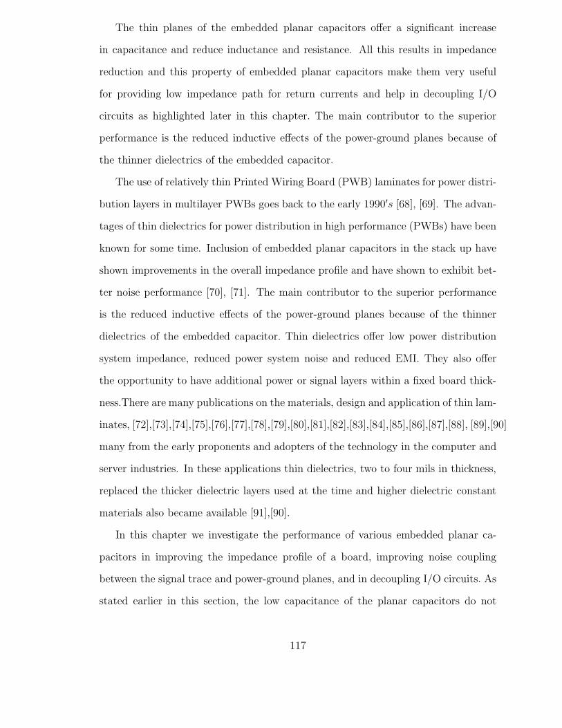
The thin planes of the embedded planar capacitors offer a significant increase
in capacitance and reduce inductance and resistance. All this results in impedance
reduction and this property of embedded planar capacitors make them very useful
for providing low impedance path for return currents and help in decoupling I/O
circuits as highlighted later in this chapter. The main contributor to the superior
performance is the reduced inductive effects of the power-ground planes because of
the thinner dielectrics of the embedded capacitor.
The use of relatively thin Printed Wiring Board (PWB) laminates for power distri-
bution layers in multilayer PWBs goes back to the early 1990′s [68], [69]. The advan-
tages of thin dielectrics for power distribution in high performance (PWBs) have been
known for some time. Inclusion of embedded planar capacitors in the stack up have
shown improvements in the overall impedance profile and have shown to exhibit bet-
ter noise performance [70], [71]. The main contributor to the superior performance
is the reduced inductive effects of the power-ground planes because of the thinner
dielectrics of the embedded capacitor. Thin dielectrics offer low power distribution
system impedance, reduced power system noise and reduced EMI. They also offer
the opportunity to have additional power or signal layers within a fixed board thick-
ness.There are many publications on the materials, design and application of thin lam-
inates, [72],[73],[74],[75],[76],[77],[78],[79],[80],[81],[82],[83],[84],[85],[86],[87],[88], [89],[90]
many from the early proponents and adopters of the technology in the computer and
server industries. In these applications thin dielectrics, two to four mils in thickness,
replaced the thicker dielectric layers used at the time and higher dielectric constant
materials also became available [91],[90].
In this chapter we investigate the performance of various embedded planar ca-
pacitors in improving the impedance profile of a board, improving noise coupling
between the signal trace and power-ground planes, and in decoupling I/O circuits. As
stated earlier in this section, the low capacitance of the planar capacitors do not
117

make them viable to decouple core circuits. The contributions of this chapter is as
follows. 1) Investigation of the impedance profile of the stack up containing embed-
ded planar capacitors with and without surface mount decoupling components along
with the model to hardware correlation. The description of the test vehicle along
with the modeling and measurement techniques will be highlighted. An analysis of
the global placement of the decoupling capacitors using a simple L − C circuit and
the prediction of the start and stop frequencies of the band-gap using the electromag-
netic band-gap concept will be done; 2) Demonstration of noise coupling suppression
between signal traces and power-ground planes is highlighted in this chapter. This
includes the description of the test vehicle designed to characterize the coupling, the
modeling, and the measurement methodology used; 3) The design of an active test
vehicle was done to show the time domain performance improvements by capturing
the noise between the power-ground plane for the different dielectric thicknesses. The
modeling and characterization methodology used to quantify the noise improvements
will be described in detail in this chapter; 4) Eye diagram simulations for different
interconnect configurations and embedded planar capacitors was done to highlight
the performance improvements with different planar embedded capacitors.
This chapter is organized as follows. Section 5.1.1 the coupling between a signal
line and the power ground planes will be described. A model will be shown based
on modal decomposition and model to measurement correlation of the measured test
vehicle will also be presented. In section 5.2.1 discusses the impedance profile variation
with the different dielectrics. The description of the test vehicle designed to capture
the differences will be highlighted in detail. The performance of the stack up with
and without the surface mount decoupling capacitors will also be investigated. In
section 5.2.5, the design of an active test vehicle to capture the simultaneous switching
noise phenomenon because of I/O return currents will be described. In section 5.3,
simulations of high speed buses with single ended and differential I/Os at data rates
118

of 1Gbps, 5Gbps and 10Gbps will be highlighted. The performance comparison of
the different embedded planar capacitor layers will be done by comparing the eye
diagrams.
5.1 Passive Test Vehicle A
This section describes the test vehicle that was designed to characterize the noise
coupling suppression between the signal trace and power-ground planes because of
the embedded planar capacitors.
5.1.1 Design and Description
The stack up of the test vehicle is shown in Fig. 95. The test vehicle was designed with
the signal via passing from the top surface of the test board through the embedded
capacitor layer to the second signal trace as shown in Fig. 96. The noise coupling from
the signal trace to the power ground planes is captured by probing the signal trace
and the power ground plane. The description and measurements of the test vehicle is
described next.
The cross section of the stack up is shown in Fig. 96. The test vehicle is a six
metal layer stack up with the planar capacitor layer sandwiched between metal layers
three and four. Metal layers one, three, and six are the ground layers. Metal layers
two and five are the signal layers and metal layer four is the power layer. The signal
layers are stripline of 50 Ω and are embedded in a 16 mil thick dielectric material of
dielectric constant 3.5. The thickness of the metal layers are 35 um each and effective
dielectric constant of the planar capacitor layer is 3.5 with a loss tangent of 0.003.
Thicknesses of the capacitor dielectric layers are 18 um, 25 um, and 50 um respectively.
These dielectric layers were used in the stack up for a board size of 6”× 6” as shown
in Fig. 95. For measurement of the power-ground impedance, probe points were
designed to access the power and ground planes in the test vehicle. Agilent’s E8363B
vector network analyzer and Cascade ACP 250 um G-S-G probes were used for the
119

Figure 95: Cross section of stack up for Passive A
measurements. A detailed analysis into the coupling between the signal trace and
the power ground plane of the stack up is done in this section. The measurement
set up, modeling technique, and model to measurement correlation of the results are
presented.
5.1.2 Measurement setup
The signal trace in Fig. 96 is excited from the surface at the first probe point (SIG
probe point). The transmission line test vehicle was designed such that the signal via
passes through the planar capacitor layer onto the signal trace SIG. The signal trace
extends for five and half inches across the board and all the ground planes in the
stack up are tied to one another by through vias. The signal trace SIG has a stripline
configuration and has a characteristic impedance of 50 Ω. The trace is referenced to a
power and ground plane as seen in Fig. 96 and the load end of the signal trace is left
unterminated. The second probe point (P-G probe point) was defined on the power-
ground plane and was defined as the receiver port. i.e. the transmitter port was
used to excite the signal trace and the coupled signal to the power ground plane was
measured using probe2. The measurements were done to investigate the performance
of all three planar capacitance materials embedded in the board.
The measured coupling results between port 1 and port 2 (S21) are plotted for
all three cases in Fig. 97. The results clearly show that the energy coupled from the
120
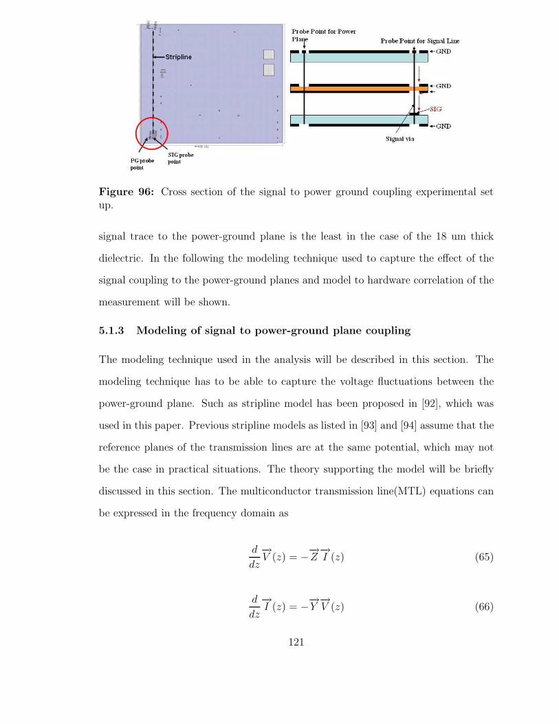
Figure 96: Cross section of the signal to power ground coupling experimental setup.
signal trace to the power-ground plane is the least in the case of the 18 um thick
dielectric. In the following the modeling technique used to capture the effect of the
signal coupling to the power-ground planes and model to hardware correlation of the
measurement will be shown.
5.1.3 Modeling of signal to power-ground plane coupling
The modeling technique used in the analysis will be described in this section. The
modeling technique has to be able to capture the voltage fluctuations between the
power-ground plane. Such as stripline model has been proposed in [92], which was
used in this paper. Previous stripline models as listed in [93] and [94] assume that the
reference planes of the transmission lines are at the same potential, which may not
be the case in practical situations. The theory supporting the model will be briefly
discussed in this section. The multiconductor transmission line(MTL) equations can
be expressed in the frequency domain as
d
dz
−→V (z) = −−→
Z−→I (z) (65)
d
dz
−→I (z) = −−→
Y−→V (z) (66)
121
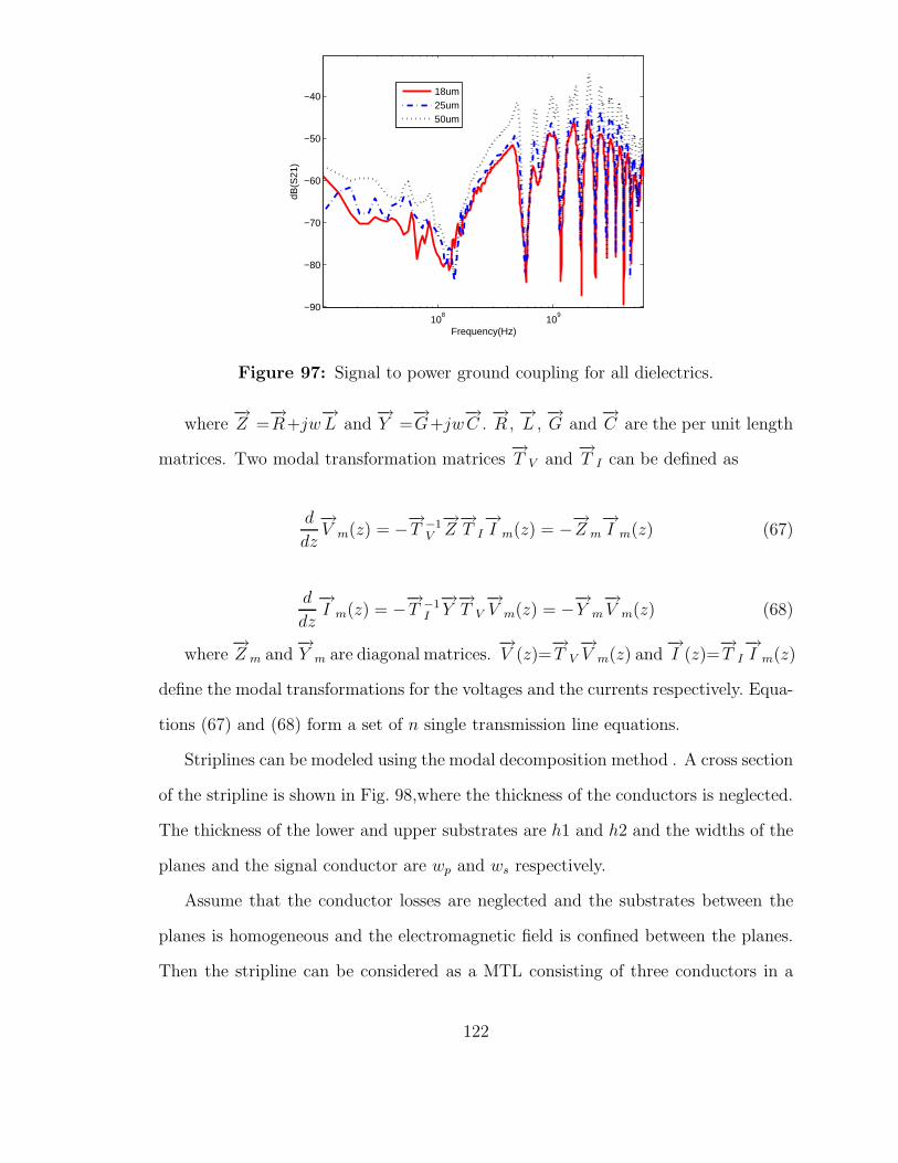
108
109
−90
−80
−70
−60
−50
−40
Frequency(Hz)
dB(S
21)
18um25um50um
Figure 97: Signal to power ground coupling for all dielectrics.
where−→Z =
−→R+jw
−→L and
−→Y =
−→G+jw
−→C .
−→R ,
−→L ,
−→G and
−→C are the per unit length
matrices. Two modal transformation matrices−→T V and
−→T I can be defined as
d
dz
−→V m(z) = −−→
T −1V
−→Z−→T I
−→I m(z) = −−→
Z m−→I m(z) (67)
d
dz
−→I m(z) = −−→
T −1I
−→Y−→T V
−→V m(z) = −−→
Y m−→V m(z) (68)
where−→Z m and
−→Y m are diagonal matrices.
−→V (z)=
−→T V
−→V m(z) and
−→I (z)=
−→T I
−→I m(z)
define the modal transformations for the voltages and the currents respectively. Equa-
tions (67) and (68) form a set of n single transmission line equations.
Striplines can be modeled using the modal decomposition method . A cross section
of the stripline is shown in Fig. 98,where the thickness of the conductors is neglected.
The thickness of the lower and upper substrates are h1 and h2 and the widths of the
planes and the signal conductor are wp and ws respectively.
Assume that the conductor losses are neglected and the substrates between the
planes is homogeneous and the electromagnetic field is confined between the planes.
Then the stripline can be considered as a MTL consisting of three conductors in a
122

Figure 98: Cross section of a stripline.
homogeneous medium. For this analysis, the bottom plane is chosen as the refer-
ence conductor. One of the initial assumptions is the modal decomposition into the
stripline and parallel plate mode. In the parallel plate mode, all of the current flowing
into one of the planes returns on the other plane, whereas in the stripline mode, which
is the intended mode of operation for signal transmission, there is no voltage differ-
ence between the planes. Since the bottom plane is chosen as the reference conductor,
these statements can be expressed in terms of the transformation matrices
−→I (z) =
(−→I p(z)−→I s(z)
)
=−→T I
−→I m(z) =
(
1 a
0 b
)(−→I par(z)−→I str(z)
)
(69)
−→V (z) =
(−→V p(z)−→V s(z)
)
=−→T V
−→V m(z) =
(
c 0
d 1
)(−→V par(z)−→V str(z)
)
(70)
where the subscripts par and str represent the parallel plane and the stripline
modes, where s and p represent the signal conductor and the upper plane, respectively.
For perfect conductors (i.e−→R=0) in a homogeneous medium,
−→C and
−→G are both
diagonalized [95], if L can be diagonalized by the transformation matrices−→T v and
−→T l as in equation (67). Therefore, in order that this choice of the transmission
matrices be appropriate, it must be shown that−→L is diagonalized by the product
−→T −1
v
−→L−→T l. By explicitly doing this multiplication, it can be shown that the
−→L is
diagonalized if the following relations hold
a = −L12
L11b (71)
123
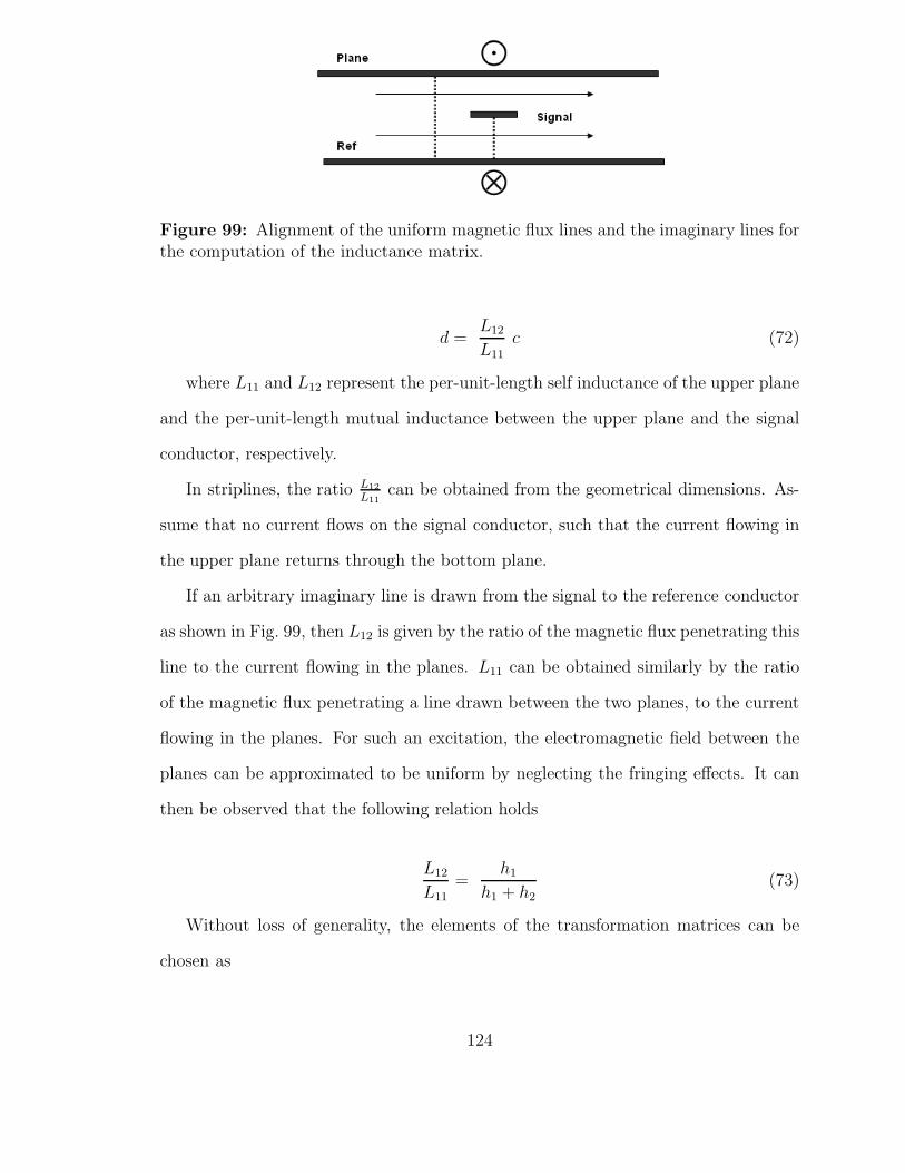
Figure 99: Alignment of the uniform magnetic flux lines and the imaginary lines forthe computation of the inductance matrix.
d =L12
L11
c (72)
where L11 and L12 represent the per-unit-length self inductance of the upper plane
and the per-unit-length mutual inductance between the upper plane and the signal
conductor, respectively.
In striplines, the ratio L12
L11
can be obtained from the geometrical dimensions. As-
sume that no current flows on the signal conductor, such that the current flowing in
the upper plane returns through the bottom plane.
If an arbitrary imaginary line is drawn from the signal to the reference conductor
as shown in Fig. 99, then L12 is given by the ratio of the magnetic flux penetrating this
line to the current flowing in the planes. L11 can be obtained similarly by the ratio
of the magnetic flux penetrating a line drawn between the two planes, to the current
flowing in the planes. For such an excitation, the electromagnetic field between the
planes can be approximated to be uniform by neglecting the fringing effects. It can
then be observed that the following relation holds
L12
L11=
h1
h1 + h2(73)
Without loss of generality, the elements of the transformation matrices can be
chosen as
124

Figure 100: Equivalent model of a stripline.
b = c = 1 (74)
a = −d = −L12
L11= − h1
h1 + h2= k (75)
An equivalent multiport model of the stripline can be found as shown in Fig. 100. Zcpar
and Zcstr represent the characteristic impedance of the parallel plate and stripline
modes respectively. The controlled sources represent the coupling between the two
modes and can be obtained from the dielectric thicknesses.
The stripline SIG was designed to be a 50 Ω line, the thickness of the dielectric
in which the stripline is embedded is 16mils thick and has a dielectric constant of
3.5, which translates into a line width of 7.1 mils for the transmission line. The
transmission line is placed at the center of the 16 mil thick dielectric. Since the
ground planes are tied together using vias, the effect of the parallel combination
of all the power ground pairs need to be taken into account. The thickness of the
dielectric in which the stripline is embedded is 16 mils (406.4 um) as compared to
the 18 um, 25 um and 50 um thick planar dielectric layers. The dielectric constant of
both materials are comparable and since they are in parallel, the capacitance of the
thinner power ground layer will dominate.
The input parameters to the power plane were obtained by modeling the power
ground plane pair using the transmission matrix method. A total of three ports
were defined in the model at the input, output and power-ground probe locations
125
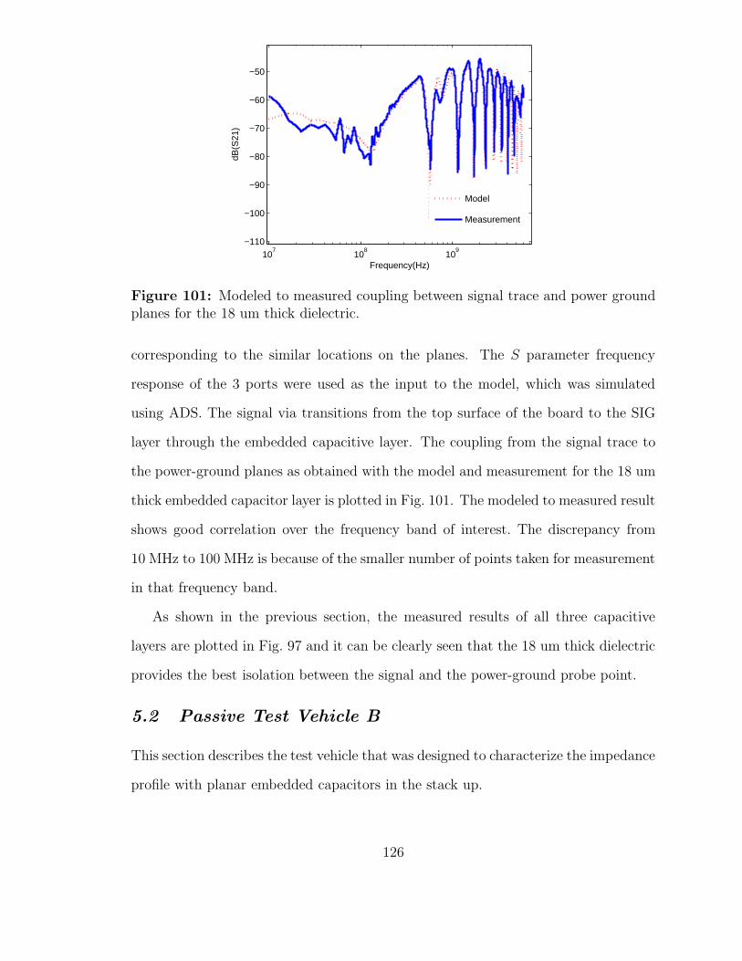
107
108
109
−110
−100
−90
−80
−70
−60
−50
Frequency(Hz)
dB(S
21)
Model
Measurement
Figure 101: Modeled to measured coupling between signal trace and power groundplanes for the 18 um thick dielectric.
corresponding to the similar locations on the planes. The S parameter frequency
response of the 3 ports were used as the input to the model, which was simulated
using ADS. The signal via transitions from the top surface of the board to the SIG
layer through the embedded capacitive layer. The coupling from the signal trace to
the power-ground planes as obtained with the model and measurement for the 18 um
thick embedded capacitor layer is plotted in Fig. 101. The modeled to measured result
shows good correlation over the frequency band of interest. The discrepancy from
10 MHz to 100 MHz is because of the smaller number of points taken for measurement
in that frequency band.
As shown in the previous section, the measured results of all three capacitive
layers are plotted in Fig. 97 and it can be clearly seen that the 18 um thick dielectric
provides the best isolation between the signal and the power-ground probe point.
5.2 Passive Test Vehicle B
This section describes the test vehicle that was designed to characterize the impedance
profile with planar embedded capacitors in the stack up.
126

Figure 102: Cross section of stack up for Passive B
5.2.1 Design and Description
The board was designed to highlight the impedance profile improvements by inclusion
of embedded planar capacitors in the stack up. The results presented in this section
are for the boards with and without surface mount discrete capacitors mounted on
the board. The cross section of the stack up is shown in Fig. 102. The stack up of
passive test vehicle B is similar to passive test vehicle A. Passive test vehicle B is a
four metal layer stack up with the planar capacitor layer sandwiched between metal
layers two and three. Metal layers one, two, and four are the ground layers and metal
layer three is the power layer. The dielectric layer between metal layer one and two
and between three and four is a 16 mil thick with a dielectric constant of 3.5. The
thickness of the metal layers are 35 um each and the effective dielectric constant
of the planar capacitor layer is 3.5 with a loss tangent of 0.003. Thicknesses of the
capacitor dielectric layers were 18 um, 25 um and 50 um respectively. These dielectric
layers were used in the stack up for a board size of 8”× 8” as shown in Fig. 95. For
measurement of the power-ground impedance, probe points were designed to access
the power and ground planes in the test vehicle. Agilent’s E8363B vector network
analyzer and Cascade ACP 250 um G-S-G probes were used for the measurements.
127
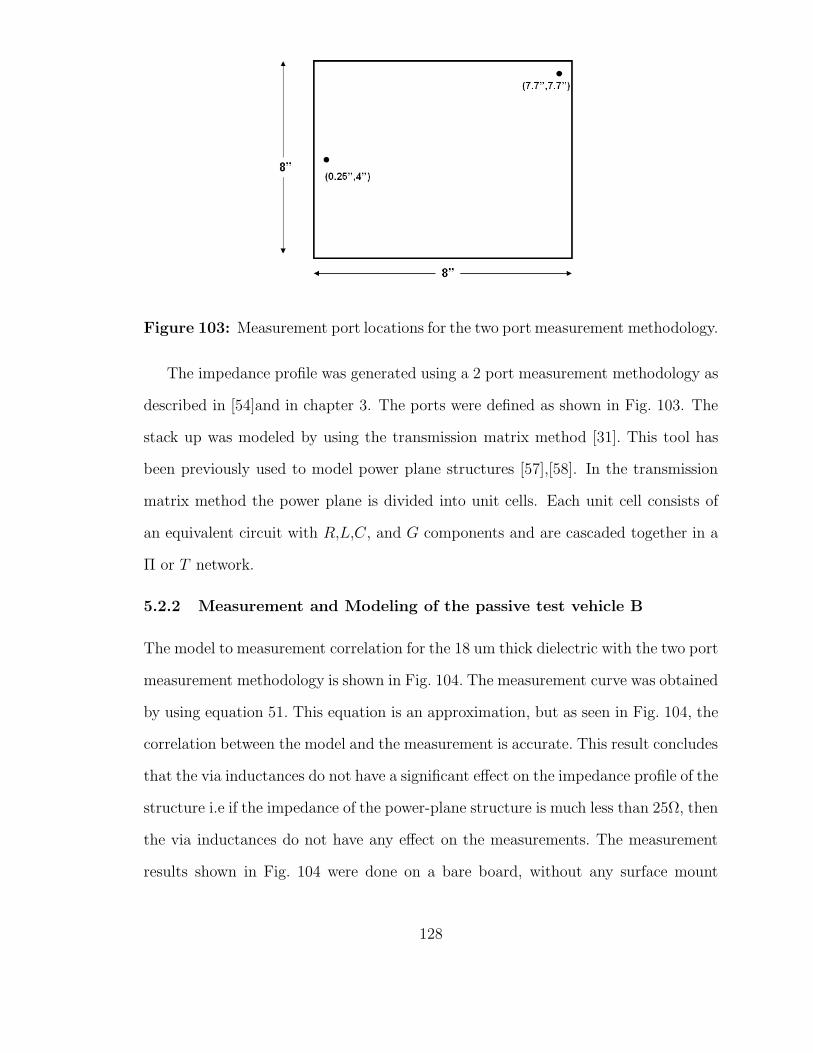
Figure 103: Measurement port locations for the two port measurement methodology.
The impedance profile was generated using a 2 port measurement methodology as
described in [54]and in chapter 3. The ports were defined as shown in Fig. 103. The
stack up was modeled by using the transmission matrix method [31]. This tool has
been previously used to model power plane structures [57],[58]. In the transmission
matrix method the power plane is divided into unit cells. Each unit cell consists of
an equivalent circuit with R,L,C, and G components and are cascaded together in a
Π or T network.
5.2.2 Measurement and Modeling of the passive test vehicle B
The model to measurement correlation for the 18 um thick dielectric with the two port
measurement methodology is shown in Fig. 104. The measurement curve was obtained
by using equation 51. This equation is an approximation, but as seen in Fig. 104, the
correlation between the model and the measurement is accurate. This result concludes
that the via inductances do not have a significant effect on the impedance profile of the
structure i.e if the impedance of the power-plane structure is much less than 25Ω, then
the via inductances do not have any effect on the measurements. The measurement
results shown in Fig. 104 were done on a bare board, without any surface mount
128
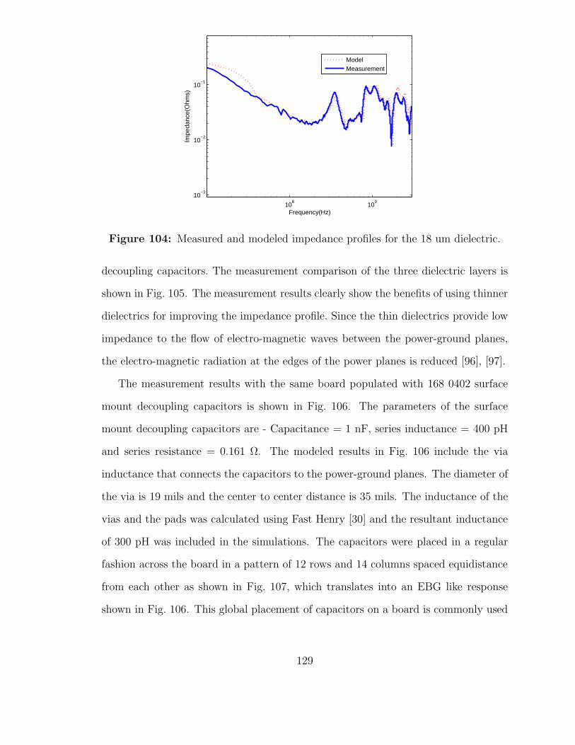
108
109
10−3
10−2
10−1
Frequency(Hz)
Impe
danc
e(O
hms)
ModelMeasurement
Figure 104: Measured and modeled impedance profiles for the 18 um dielectric.
decoupling capacitors. The measurement comparison of the three dielectric layers is
shown in Fig. 105. The measurement results clearly show the benefits of using thinner
dielectrics for improving the impedance profile. Since the thin dielectrics provide low
impedance to the flow of electro-magnetic waves between the power-ground planes,
the electro-magnetic radiation at the edges of the power planes is reduced [96], [97].
The measurement results with the same board populated with 168 0402 surface
mount decoupling capacitors is shown in Fig. 106. The parameters of the surface
mount decoupling capacitors are - Capacitance = 1 nF, series inductance = 400 pH
and series resistance = 0.161 Ω. The modeled results in Fig. 106 include the via
inductance that connects the capacitors to the power-ground planes. The diameter of
the via is 19 mils and the center to center distance is 35 mils. The inductance of the
vias and the pads was calculated using Fast Henry [30] and the resultant inductance
of 300 pH was included in the simulations. The capacitors were placed in a regular
fashion across the board in a pattern of 12 rows and 14 columns spaced equidistance
from each other as shown in Fig. 107, which translates into an EBG like response
shown in Fig. 106. This global placement of capacitors on a board is commonly used
129
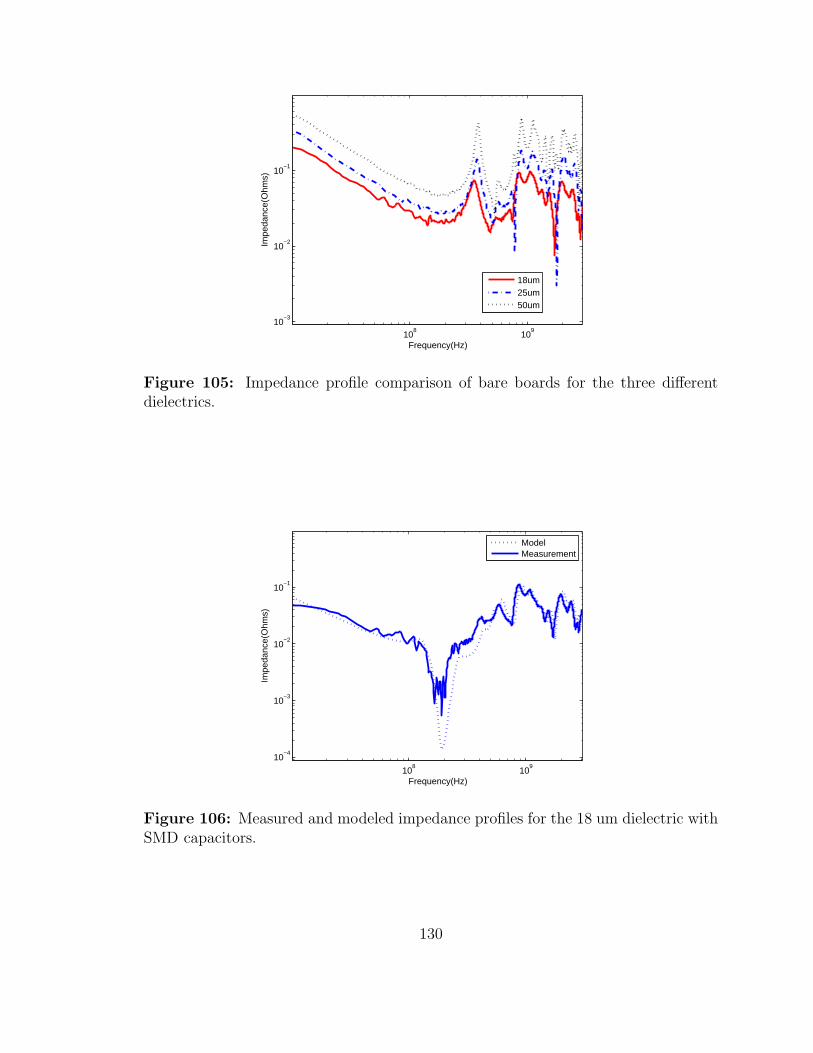
108
109
10−3
10−2
10−1
Frequency(Hz)
Impe
danc
e(O
hms)
18um25um50um
Figure 105: Impedance profile comparison of bare boards for the three differentdielectrics.
108
109
10−4
10−3
10−2
10−1
Frequency(Hz)
Impe
danc
e(O
hms)
ModelMeasurement
Figure 106: Measured and modeled impedance profiles for the 18 um dielectric withSMD capacitors.
130
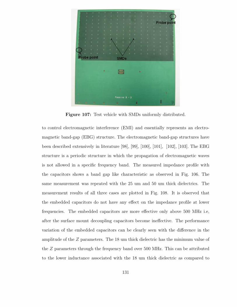
Figure 107: Test vehicle with SMDs uniformly distributed.
to control electromagnetic interference (EMI) and essentially represents an electro-
magnetic band-gap (EBG) structure. The electromagnetic band-gap structures have
been described extensively in literature [98], [99], [100], [101], [102], [103]. The EBG
structure is a periodic structure in which the propagation of electromagnetic waves
is not allowed in a specific frequency band. The measured impedance profile with
the capacitors shows a band gap like characteristic as observed in Fig. 106. The
same measurement was repeated with the 25 um and 50 um thick dielectrics. The
measurement results of all three cases are plotted in Fig. 108. It is observed that
the embedded capacitors do not have any effect on the impedance profile at lower
frequencies. The embedded capacitors are more effective only above 500 MHz i.e,
after the surface mount decoupling capacitors become ineffective. The performance
variation of the embedded capacitors can be clearly seen with the difference in the
amplitude of the Z parameters. The 18 um thick dielectric has the minimum value of
the Z parameters through the frequency band over 500 MHz. This can be attributed
to the lower inductance associated with the 18 um thick dielectric as compared to
131

108
109
10−3
10−2
10−1
Frequency(Hz)
Impe
danc
e(O
hms)
18um25um50um
Figure 108: Measured impedance profiles for all the dielectric with SMD capacitors.
the 25 um and 50 um thick dielectrics. The comparison of the impedance profiles of
different dielectrics with and without the SMDs is show in Fig. 109 and Fig. 110. The
comparison is between the populated 50 um thick dielectric and the bare 25 um board
and bare 18 um board respectively. The impedance profile clearly shows the benefits
of the SMDs in lower frequency region. Above 500 MHz the benefits of the thinner
dielectrics is obvious because of the reduced inductance of the planes.
5.2.3 Analysis of band-gap characteristic
An analysis was done to determine the band gap characteristic of the stack up with
the SMDs. The SMDs are attached to the power -ground plane which is 18 um
thick and has a dielectric constant of 3.5 contributing a total capacitance of 69 nF.
To analyze the stack up, the power-ground pair around which the capacitors were
mounted was assumed to be divided into 168 equal parts. The resultant unit cell is
shown in Fig. 111. The resonant frequency of the band gap of the resultant unit cell
can be calculated by equation (76):
132

107
108
109
1010
10−4
10−3
10−2
10−1
100
Frequency(Hz)
Impe
danc
e(O
hms)
Populated 50um boardBare 25um board
Figure 109: Measured impedance profile comparison of a bare 25 um and populated50 um board.
107
108
109
1010
10−4
10−3
10−2
10−1
100
Frequency(Hz)
Impe
danc
e(O
hms)
Populated 50um boardBare 18um board
Figure 110: Measured impedance profile comparison of a bare 18 um and populated50 um board.
133

f =1
2π√
L1C1
(76)
C1 is the capacitance of an individual SMD in the unit cell and L1 is the inductance
of the SMD capacitor. The resonant frequency was calculated as 190.2 MHz and is
captured in the measurements. The effective resistance of the capacitor array is
calculated by dividing the series resistance of one capacitor by the total number of
capacitors. Therefore, the effective resistance of the capacitor array is 0.95 mΩ as
can be seen in Fig. 106.
The measurement results of the global placement of the capacitors show a band
gap like result. Therefore, to predict the start and stop frequencies of the band gap
an equivalent circuit model of the meshed structure was formed and analyzed, similar
to the methodology used in [104]. The stopband and passband properties of the EBG
structure could be understood through a circuit analysis of only one unit cell. The
capacitor and the via inductance present a shunt susceptance given by
Y =jωC1
1 − ω2L1C1(77)
The two dimensional periodic structure is simplified to an array of one dimensional
unit cells as shown in Fig. 111
The TEM mode excited within a unit cell of height h and width d is modeled as a
simple parallel plate transmission line of characteristic impedance and phase constant
given by following equations:
Zo =ηo√ǫ
h
d(78)
β =ω
c
√ǫ (79)
where ηo is the wave impedance of free space (377 Ω), c is the speed of light in
134

Figure 111: Transmission line for one unit cell in the approximated EBG structure.
vacuum, ω is the radian frequency and the ǫ (3.5) is the dielectric constant of the
power-ground unit cell. To predict the dispersive behavior of this structure, the unit
cell can be analyzed by using the ABCD parameters, where the unit cell has the
effective phase constant kx as
A B
C D
=
cos(kxd) jZosin(kxd)
jYosin(kxd) cos(kxd)
=
cos(β d2) jZosin(β d
2)
jYosin(β d2) cos(β d
2)
1 0
Y 1
cos(β d2) jZosin(β d
2)
jYosin(β d2) cos(β d
2)
Evaluation of the A component yields the dispersive equation
cos(kxd) = cos(βd) + jZoY
2sinβd (80)
From equation (80) we can explicitly solve for the effective phase constant kx
135

0 2 4 6 8 10
x 108
0
0.5
1
1.5
2
2.5
3
3.5
4
4.5
Frequency(Hz)
Atte
nuat
ion
per
Uni
t Cel
l(dB
)
Figure 112: Calculated attenuation per unit cell of the EBG structure.
kx =1
dcos−1[cosβd − ωC1Zo
2(1 − ω2L1C1)sinβd] (81)
From the above equation, the attenuation can be calculated as follows.
Attn = −20log10(e−αxd) (82)
where, αx is the real part of the effective phase constant kx and the field decay
over one unit cell is e−αxd. This quantity has been expressed as the power attenuation
per unit cell in decibels using equation (82). This quantity is plotted in Fig. 112,
the regions where the attenuation constant is non-zero is the stop band of the peri-
odic structure. According the values in the Fig. 112 the stopband should exist from
approximately 170 MHz to 400 MHz, however the measured stop-band for the 18 um
dielectric exists from 130 MHz to 300 MHz. There is a difference between the pre-
dicted and the measured values, since a simple 1D unit-cell approach was used to
generate the attenuation plot.
136

Figure 113: Cross section of active test vehicle.
5.2.4 Active Test Vehicle
An active test vehicle was designed using the embedded capacitor layers to inves-
tigate their performance in the time domain. The test vehicle consisted of a clock
generator, transmission lines, termination resistors and probe points to measure the
power-ground noise as well as the clock signal.
5.2.5 Description of the active test vehicle
The cross section of the active test vehicle showing the signal path is shown in
Fig. 113. The stack up of the signal is identical to that of Passive test vehicle A.
The test vehicle consists of two stripline configurations. The upper SIG layer has
two ground planes as its reference planes while the bottom SIG layer has a power
and ground plane as its references as shown in Fig. 113.
The length of the transmission line from the driver to the termination resistor is
20 inches and the width of the reference planes are 1 inch. A 100 MHz clock oscillator
was used as the input excitation signal. The transmission line on the signal trace was
designed to be 50 Ω. The dielectric constant and the thickness in which the trans-
mission lines were embedded were identical (i.e, the thickness and dielectric constant
of the material are 16 mils and 3.5 respectively). The width of the transmission line
is 7.1 mils and the thickness of copper on all planes is 1.4 mils. The test vehicle
137
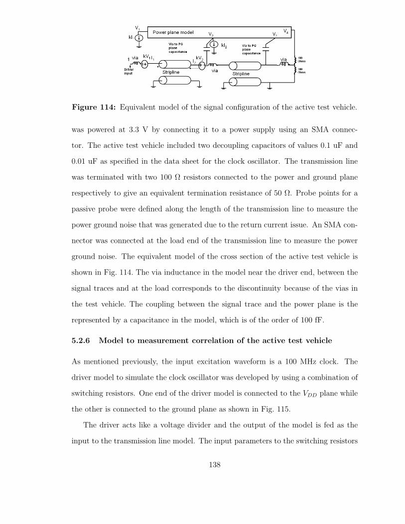
Figure 114: Equivalent model of the signal configuration of the active test vehicle.
was powered at 3.3 V by connecting it to a power supply using an SMA connec-
tor. The active test vehicle included two decoupling capacitors of values 0.1 uF and
0.01 uF as specified in the data sheet for the clock oscillator. The transmission line
was terminated with two 100 Ω resistors connected to the power and ground plane
respectively to give an equivalent termination resistance of 50 Ω. Probe points for a
passive probe were defined along the length of the transmission line to measure the
power ground noise that was generated due to the return current issue. An SMA con-
nector was connected at the load end of the transmission line to measure the power
ground noise. The equivalent model of the cross section of the active test vehicle is
shown in Fig. 114. The via inductance in the model near the driver end, between the
signal traces and at the load corresponds to the discontinuity because of the vias in
the test vehicle. The coupling between the signal trace and the power plane is the
represented by a capacitance in the model, which is of the order of 100 fF.
5.2.6 Model to measurement correlation of the active test vehicle
As mentioned previously, the input excitation waveform is a 100 MHz clock. The
driver model to simulate the clock oscillator was developed by using a combination of
switching resistors. One end of the driver model is connected to the VDD plane while
the other is connected to the ground plane as shown in Fig. 115.
The driver acts like a voltage divider and the output of the model is fed as the
input to the transmission line model. The input parameters to the switching resistors
138

Figure 115: Driver model used to generate square wave.
0 1 2 3 4 5 6 7 8
x 10−8
0
0.5
1
1.5
2
2.5
3
Time(sec)
Vol
tage
(V)
MeasModel
Artifact of Measurement−Loopinductance of passive probe
Figure 116: Model to measurement correlation of the input waveform.
are the rise, fall and time period of the 100 MHz clock. The model to measurement
correlation of the input pulse in the time domain and frequency domain are shown in
Fig. 116 and Fig. 117 respectively. The spike observed in the measured result is due
to the loop inductance of the signal-ground loop in the passive probe used to probe
the output pin of the clock oscillator.
The model included the via inductance from the top surface to the bottom SIG
layer, the via inductance between the two signal layers and the via coupling between
the signal via and the power ground plane. The measurement was done by connecting
139
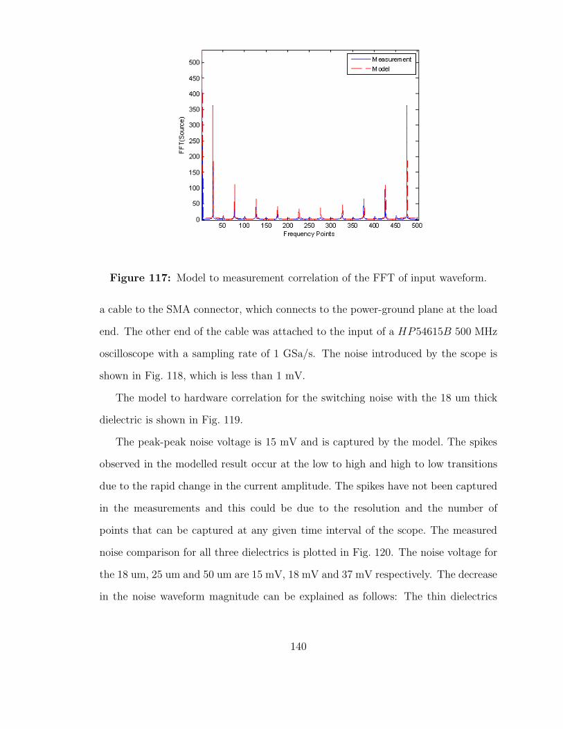
Figure 117: Model to measurement correlation of the FFT of input waveform.
a cable to the SMA connector, which connects to the power-ground plane at the load
end. The other end of the cable was attached to the input of a HP54615B 500 MHz
oscilloscope with a sampling rate of 1 GSa/s. The noise introduced by the scope is
shown in Fig. 118, which is less than 1 mV.
The model to hardware correlation for the switching noise with the 18 um thick
dielectric is shown in Fig. 119.
The peak-peak noise voltage is 15 mV and is captured by the model. The spikes
observed in the modelled result occur at the low to high and high to low transitions
due to the rapid change in the current amplitude. The spikes have not been captured
in the measurements and this could be due to the resolution and the number of
points that can be captured at any given time interval of the scope. The measured
noise comparison for all three dielectrics is plotted in Fig. 120. The noise voltage for
the 18 um, 25 um and 50 um are 15 mV, 18 mV and 37 mV respectively. The decrease
in the noise waveform magnitude can be explained as follows: The thin dielectrics
140
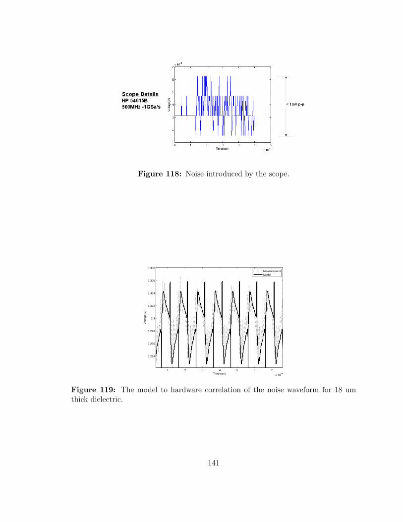
Figure 118: Noise introduced by the scope.
1 2 3 4 5 6 7
x 10−8
3.294
3.296
3.298
3.3
3.302
3.304
3.306
3.308
Time(sec)
Vol
tage
(V)
MeasurementModel
Figure 119: The model to hardware correlation of the noise waveform for 18 umthick dielectric.
141

1.95 2 2.05 2.1 2.15 2.2 2.25 2.3 2.35
x 10−7
3.28
3.285
3.29
3.295
3.3
3.305
3.31
3.315
Time(sec)
Vol
tage
(V)
50um25um18um
37mV
18mV 15mV
Figure 120: Noise voltage comparison for the 3 dielectrics.
have a two fold advantage, the capacitance of the structure increases for the same
dielectric as given by the equation (83):
C =ǫoǫrA
d(83)
where, ǫo is the relative dielectric constant of the dielectric, A is the area of the
capacitive structure and d is separation between the plates of the structure. Also, the
inductance of the same structure, which is given by (84) reduces due to a decrease in
the separation between the plates.
L = µod (84)
The effective increase in the capacitance and decrease in the inductance leads to
an overall decrease in the impedance of the power planes as given by equation (85):
Z =
√
L
C(85)
Electromagnetic waves propagating through the power-ground plane will see a reduced
impedance, therefore generating less noise voltage as per ohms law.
The normalized noise voltage with respect to the thickness in plotted in Fig. 121.
The model and the measured results agree very well. The modeled result is plotted
142

15 20 25 30 35 40 45 500.4
0.5
0.6
0.7
0.8
0.9
1
Dielectric Thickness (um)
Nor
mal
ized
noi
se v
olta
ge
MeasurementModel
Figure 121: The modeled and measured normalized noise voltage.
1 2 3 4 5 6 7 8 9 10
x 10−8
0.5
1
1.5
2
2.5
Time(sec)
Vol
tage
(V)
measmodel
Figure 122: Load waveform for the 18 um thick dielectric.
as a straight solid line and the measured result is plotted as a circle. The model to
measurement correlation for the load waveform for the 18 um dielectric is plotted in
Fig. 122.
5.3 Benefits of Embedded Planar Capacitors in System Ap-plications
This section describes the simulations carried out for I/O configurations present in
todays high data rate digital systems. The configurations were single and differential
bus configurations with data rates of 1 Gb/s, 5 Gb/s and 10 Gb/s. The transmis-
sion line in these simulations were in the stripline configuration and were terminated
143

Figure 123: Simulation set up for the 16 bit FSB.
Table 11: Dielectrics used in the SSN and eye opening simulationsDielectric thickness(um) Dielectric constant Loss Tangent
8 3.5 0.00312 3.5 0.00318 3.5 0.00325 3.5 0.00350 4.2 0.01550 3.5 0.008
differentially with matched loads.
5.3.1 Single Ended Stripline Configuration
The first configuration was of a 16 bit Front Side bus (FSB). This configuration
consists of 16 50 Ω uncoupled single ended transmission lines terminated differentially
at the load end with two 100 Ω resistors to give an effective termination of 50 Ω. The
model used in this simulation was similar to the stripline model used in the passive
test vehicle. The length of transmission line is 200 mm and the dimensions of reference
planes are 200 mm by 200 mm. The methodology used to carry out the simulations
was similar to the method mentioned in the previous sections. The simulation set up
is shown in Fig. 123. The different dielectric layers used in the simulations are listed
in table 11.
The simulation for the FSB was done with pseudo random sources (PRBS) at
1 Gb/s. The rise and fall times of the source was 200 psec with a 1 V voltage
swing. The driver model used was similar to the driver models used in the active test
144

Table 12: SSN variation with different dielectrics at 1Gb/sDielectric thickness(um) Dielectric constant SSN peak to peak magnitude(mV)
8 3.5 23712 3.5 41418 3.5 44525 3.5 48950 4.2 96850 3.5 980
50 + 100 × 100nF decaps 3.5 695
vehicles. The variation in the SSN is listed in table 12
The last row in table 12, refers to the case when a simulation was carried out
with the 50 um thick dielectric, with a dielectric constant of 3.5 and 100 decoupling
capacitors with C=100 nF, ESR=0.03 Ω and ESL=400 pH scattered around the driver
end, receiver end and along the length of the transmission line. The effectiveness of
the different planar capacitors can be compared by their eye diagrams. Fig. 124
and Fig. 125, compare the eye diagrams of the last 2 rows of table 12 respectively.
The improvements in the eye diagrams are evident with the decoupling capacitors.
However, the performance improvement can be enhanced considerably when a 18 um
thick dielectric with a dielectric constant of 3.5 is used as shown in Fig. 127. From
the above results it can be inferred that for decoupling I/O circuits planar embedded
capacitors can be more effective compared to using individual decoupling capacitors.
Eye diagram and SSN simulations for the above dielectrics listed in table 12 are
included in Appendix A at the end of thesis.
5.3.2 Differential Microstrip Configuration
Similar analysis was done for a 4 pair differential microstrip configuration. The simu-
lation data rates used were 5 Gb/s and 10 Gb/s with PRBS input waveforms having
a voltage swing of 1V. The rise and fall times for a 5 Gb/s driver model were 40 psec
with a skew of 10 psec between the 2 differential signals. The common mode and dif-
ferential mode resistance of the transmission lines were 50 Ω and 100 Ω respectively.
145

Figure 124: Eye diagram result for row 7 of table 12, 50 um dielectric planarcapacitor at a data rate of 1 Gbps.
Figure 125: Eye diagram result for row 8 of table 12, 50 um planar capacitor with100 decoupling capacitors at a data rate of 1 Gbps.
Figure 126: Eye diagram result for row 4 of table 12, 18 um dielectric planarcapacitor at a data rate of 1 Gbps.
146
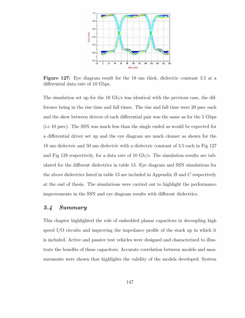
Figure 127: Eye diagram result for the 18 um thick, dielectric constant 3.5 at adifferential data rate of 10 Gbps.
The simulation set up for the 10 Gb/s was identical with the previous case, the dif-
ference being in the rise time and fall times. The rise and fall time were 20 psec each
and the skew between drivers of each differential pair was the same as for the 5 Gbps
(i.e 10 psec). The SSN was much less than the single ended as would be expected for
a differential driver set up and the eye diagram are much cleaner as shown for the
18 um dielectric and 50 um dielectric with a dielectric constant of 3.5 each in Fig 127
and Fig 128 respectively, for a data rate of 10 Gb/s. The simulation results are tab-
ulated for the different dielectrics in table 13. Eye diagram and SSN simulations for
the above dielectrics listed in table 13 are included in Appendix B and C respectively
at the end of thesis. The simulations were carried out to highlight the performance
improvements in the SSN and eye diagram results with different dielectrics.
5.4 Summary
This chapter highlighted the role of embedded planar capacitors in decoupling high
speed I/O circuits and improving the impedance profile of the stack up in which it
is included. Active and passive test vehicles were designed and characterized to illus-
trate the benefits of these capacitors. Accurate correlation between models and mea-
surements were shown that highlights the validity of the models developed. System
147

Figure 128: Eye diagram result for the 50 um thick, dielectric constant 3.5 at adifferential data rate of 10 Gbps.
Table 13: SSN variation with different dielectrics at 5 Gb/s and 10 Gb/s for a fourpair differential microstrip configuration.
Dielectric thickness(um) Dielectric constant SSN peakto peakmagni-tude(mV)at 5Gb/s
SSN peakto peakmagni-tude(mV)at 10Gb/s
8 3.5 8 4412 3.5 29.4 7418 3.5 89.5 106.525 3.5 128 15750 4.2 200 27850 3.5 225 280
148

Table 14: Performance variation with different dielectrics at 1 Gb/s 16 bit Singleended strip-line configuration.
Dielectric thickness(um) Dielectric constant Jitter (ps) Eye Height (V)18 3.5 82.6 0.8050 3.5 298.54 0.69
50 + 100 X 100nF decaps 3.5 275 0.72
Table 15: Performance variation with different dielectrics at 5 Gb/s and 10 Gb/sfor a four pair differential micro-strip configuration.Dielectric thickness(um) Dielectric constant Data rate(Gb/s) Jitter( ps) Eye
Height(V)
18 3.5 5 1.95 0.8850 3.5 5 3.91 0.8618 3.5 10 3.9 0.8150 3.5 10 15.1 0.83
simulations of single ended and differential bus configurations was done at different
data rates to highlight the performance improvements achievable by using embedded
planar capacitors. The improvements were quantified by comparing the eye diagrams
and SSN for the different cases. Tables 14 and 15 capture the improvement in perfor-
mance of the system applications by using different embedded capacitors.
149

CHAPTER VI
CONCLUSION AND FUTURE WORK
The increase in clock frequency and power dissipation of processors has put strin-
gent requirements on the design of power distribution networks. The simultaneous
switching of output drivers or logic circuits of a microprocessors generate noise that
can deteriorate the performance of sensitive circuits. A large noise spike close to the
operating frequency of the device can de-sensitize the circuit and destroy its func-
tionality. Charge must be provided with the least amount of inductance to prevent
any malfunctioning of the circuits. To do this, target impedances in the order of sub
milli-ohms have to be met over a frequency range that spans from DC to multiples
of chip operating frequency. A case for using embedded capacitors in the package to
decouple core logic in the mid-band frequency from 100 MHz to 2 GHz for processors
has been shown in this thesis.
Individual embedded capacitors developed on the hydrothermal process at PRC
and at DuPont were measured, modeled, and characterized. The benefits of using the
individual sized capacitors can be made based on decoupling implications for a digital
package using the System on Package approach, with no board but only the package
as the system.
In a digital package using the SOP concept, the power supplied is from within the
package because of the absence of the board. This is advantageous from a decoupling
perspective because the inductive effects of the board are removed. However bringing
the voltage supply closer the active circuits (chip) does not imply that all the charge
can be provided from the power supply at all frequencies of operation as explained in
the following paragraph. The VRM is connected to the power supply and converts
150
one DC voltage level to another. It senses the voltage near the load and adjusts
the output current to regulate the load voltage. The VRM consists of a switching
regulator that charges and discharges based on the voltage sensed at the load. The
rate of switching of the regulator depends on the rate of change of the load voltage.
Therefore, even if we were to place the VRMs right next to the active circuits, the
switching regulators would need to operate at a very high frequency (100s of MHz to
the GHz) range to be able to satisfy the decoupling requirements of circuits operating
at that frequency. The VRM on the board with today’s technology is effective only
from 1 KHz to hundreds of KHz. However, the placement of the VRM on the package
would extend its operation to the lower 10’s of MHz region (because of the reduced
inductance effects) minimizing the need for some of the high value capacitors that
were placed on the board. Decoupling also needs to be provided from the 10’s of MHz
region to multiples of chip operating frequency. For frequencies above 1 GHz on-chip
decoupling capacitors is used since high capacitance values in the order of 100’s of
nF are required to decouple in the high MHz region which reduces the real estate
available for logic circuitry. Therefore, the frequency band from the MHz to the GHz
region has to be decoupled from the package.
With such a SOP scenario there a variety of decoupling options as listed below: 1)
Low inductance surface mount individual capacitors can be placed on the surface of
the package to target frequencies that cannot be met by using VRMs. Since they are
spread horizontally on the package and away from the processor the inductive loop
associated with the current flow of the capacitors will prevent them from targeting
higher frequency bands. To target frequencies in the region of 100s of MHz, the loop
inductance would further need to be reduced and this can be achieved by placing
the charge carriers closer to the active circuits. 2) SMD individual capacitors can
be embedded but the frequency band that can be targeted is limited because of the
limited real estate under the die shadow. 3) A capacitance interposer between the
151

chip and the package can be used. The routing of the signal traces is an issue since
they would need to pass through a high K dielectric material increasing the coupling
between the signal trace and the capacitor layers. The signal traces can be shielded by
placing low k dielectric materials around them. 4) A thin high K dielectric capacitor
layer with dimensions equal to the die shadow can be placed in one of the package
layers. The drawback of this approach is that the bandwidth that can be targeted
with this lumped capacitor with different number of via pairs is small compared to
the bandwidth obtainable with an array of capacitors as shown in Fig. 129. 5) The
required frequency band in the 100s of MHz to the GHz range can be targeted by
embedding thin film variable sized capacitors within the package.
Based on the models developed in this thesis , an array of embedded capacitors
within the package was proposed to meet a target impedance of 2 mohms to decouple
active circuits in the mid-band frequency range of 100 MHz - 2 GHz. The performance
comparison of a single capacitor the size of a die shadow was done with an array of
capacitors. The simulation results of the comparison are shown in Fig. 129, which
shows the impedance profile of an array of capacitors as compared to a single capacitor
of size 10 mm a side with 68 via pairs attached to it. The difference in the frequency
band that can be targeted is clearly observed from the resultant simulation.
An investigation into the performance improvements of I/O decoupling using
embedded planar capacitors was conducted in this thesis. A test vehicle was de-
signed, fabricated, and measured to quantify the plane to plane noise waveforms. Plane
bounce represents the potential variation between the voltage and the ground nodes
across the surface of the planes. Models of the transmission lines were developed
based on modal decomposition and were coupled with the power-ground plane mod-
els. Model to measurement correlation was obtained for the SSN as well as the
isolation between the signal trace and the power-ground planes for different dielectric
thicknesses of the embedded capacitors. The modeling methodology accounted for
152
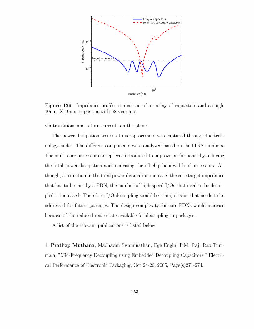
109
10−3
10−2
frequency (Hz)
Impe
danc
e(O
hms)
Array of capacitors10mm a side square capacitor
Target Impedance
Figure 129: Impedance profile comparison of an array of capacitors and a single10mm X 10mm capacitor with 68 via pairs.
via transitions and return currents on the planes.
The power dissipation trends of microprocessors was captured through the tech-
nology nodes. The different components were analyzed based on the ITRS numbers.
The multi-core processor concept was introduced to improve performance by reducing
the total power dissipation and increasing the off-chip bandwidth of processors. Al-
though, a reduction in the total power dissipation increases the core target impedance
that has to be met by a PDN, the number of high speed I/Os that need to be decou-
pled is increased. Therefore, I/O decoupling would be a major issue that needs to be
addressed for future packages. The design complexity for core PDNs would increase
because of the reduced real estate available for decoupling in packages.
A list of the relevant publications is listed below-
1. Prathap Muthana, Madhavan Swaminathan, Ege Engin, P.M. Raj, Rao Tum-
mala, ”Mid-Frequency Decoupling using Embedded Decoupling Capacitors.” Electri-
cal Performance of Electronic Packaging, Oct 24-26, 2005, Page(s)271-274.
153

2. Prathap Muthana, Madhavan Swaminathan, Rao Tummala, V.Sundaram, Lixi
Wan, S.K. Bhattacharya, P.M. Raj, ”Packaging of Multi-Core processors: Trade-
off’s and Potential Solutions.” Electronic Components and Technology Conference,
May31-June3, 2005, Vol2, Page(s) 1895-1903.
3. Prathap Muthana, Madhavan Swaminathan, Ege Engin, Rao Tummala, P.M.Raj, Lixi
Wan, D. Balaraman, S.Bhattacharya, ”Design, Modeling and Characterization of Em-
bedded Capacitor Networks for Mid-Frequency Decoupling in Semiconductor Sys-
tems.” Electromagnetic Compatibility, August 2005, Page(s)638-643.
4. Prathap Muthana, Ege Engin, Madhavan Swaminathan, Rao Tummala, Venkatesh
Sundaram, Lixi Wan, S.K Bhattacharya, P.M. Raj, K.J. Lee, Mahesh Vardarajan, Isaac
Robin Abothu, ”Measurement, Modeling and Characterization of Embedded Capac-
itors for Power Delivery in the Mid Frequency Range.” IMAPS, 2005.
5. Prathap Muthana, Erdem Matoglu, Nam Pham, Daniel N de Araujo, Bhyrav
Mutnury, Moises Cases and Madhavan Swaminathan, ”Analysis of Embedded Pack-
age Capacitors for High Performance Components.” EPEP, 2006.
6. Prathap Muthana, Krishna Srinvasan, Ege Engin, Madhavan Swaminathan, Rao
Tummala, Daniel Amey, Karl Dietz and Sounak Banerji, ”I/O decoupling in High
Speed Packages Using Embedded Planar Capacitors.” Accepted for publication at
ECTC 2007.
154

7. Prathap Muthana, Ege Engin, Madhavan Swaminathan, P.M. Raj, Rao Tum-
mala, Venkatesh Sundaram, Daniel Amey, Karl Dietz, Sounak Banerji, M. Cases, ”De-
sign Modeling and Characterization of Embedded Capacitors for Decoupling Appli-
cations.” Proceedings of IBM Center for Advance Studies Conference Feb 2006.
8. Prathap Muthana, Ege Engin, Madhavan Swaminathan, Venkatesh Sundaram,
P.Markondeya Raj, Daniel Amey, Karl Dietz, Sounak Banerji and Rao Tummala, ”De-
sign, Modeling and Characterization of Embedded Capacitor Networks in the Mid-
Band Frequency Range”. Accepted for publication in IEEE Transactions on Advanced
Packaging.
9. Prathap Muthana, Krishna Srinivasan, Ege Engin, Madhavan Swaminathan, Venkatesh
Sundaram, Daniel Amey, Karl Dietz, Sounak Banerji and Rao Tummala, ”Improve-
ments in Noise Suppression for I/O circuits Using Embedded Planar Capacitors”. Sub-
mitted for publication in IEEE Transactions on Advanced Packaging.
10. P.Markondeya Raj, Prathap Muthana, T.Danny Xiao, Lixi Wan, Devarajan
Balaraman, Isaac Robin Abothu, Swapan Bhattacharya, Madhavan Swaminathan
and Rao Tummala, ”Magnetic Nanocomposites for Organic Compatible Miniaturized
Antennas and Inductors.” Advanced Packaging Materials: Processes, Properties and
Interfaces, 2005, 16-18 March, Page(s)272-275.
11. Krishna Srinivasan, Prathap Muthana, R.Manderaker, E.Engin, J. Choi and
M.Swaminathan, ”Enhancement of Signal Integrity and Power Integrity with Embed-
ded Capacitors in High Speed Packages” ISQED 2006.
12. Lixi Wan, Prathap Muthana, D.Balaraman, P.M.Raj, S.K. Bhattacharya, M.
155
Vardarajan, I.R. Abothu, M.Swaminathan and Rao Tummala, ”Embedded Decou-
pling Capacitor Performance in High Speed Circuits.” ECTC 2005, page(s)1617-
1622. Vol 2.
13. Lee, K.J.; Bhattacharya, S.; Varadarajan, M.; Lixi Wan; Abothu, I.R.; Sun-
daram, V.; Muthana, P; Balaraman, D.; Raj, P.M.; Swaminathan, M.; Sitaraman,
S.; Tummala, R.; Viswanadham, P.; Dunford, S.; Lauffer, J.”Design, fabrication, and
reliability assessment of embedded resistors and capacitors on multilayered organic
substrates.” Advanced Packaging Materials: Processes, Properties and Interfaces,
2005. Proceedings. International Symposium on 16-18 March 2005 Page(s):249 - 254.
14. Christian Schuster, Young Kwark, Giuseppe Selli and Prathap Muthana,”Developing
a Physical Model for Vias.” DesignCon 2006.
A list of the patents that were filed as a result of this work are listed below:
Prathap Muthana, M. Swaminathan, A. E. Engin, and L. Wan, ”A package hav-
ing an array of embedded capacitors for power delivery and decoupling in the mid-
frequency range and methods of forming thereof - United States Patent Application:
EL0624USNA, ” August 31, 2006.
Prathap Muthana, A.E. Engin, M. Swaminathan, and K. Srinivasan, ”A package
having an array of embedded capacitors for power delivery and decoupling of high
speed input/output circuit and methods of forming thereof - United States Patent
Application: EL0629USNA, ” August 31, 2006
As a continuation of the work described in this thesis, the following areas of study
may be considered.
156

(a) Design, fabrication, and characterization of a prototype with an array of individ-
ual embedded capacitors. The performance benefits in the time and frequency domain
were highlighted for an array of individual sized embedded package capacitors through
simulations. The fabrication of an actual prototype which could be used for perfor-
mance verifications would aid in optimizing the design of the array and also aid in
developing measurement methodologies to characterize such a complex structure.
(b) A re-workable design of the embedded capacitor array that could be used for suc-
cessive generations of processors. Since the power requirements of processors would
change through technology nodes, which translates into different decoupling require-
ments. A re-workable design and fabrication methodology that could be used through
successive product generations would be beneficial in time and cost savings.
157

APPENDIX A
SIMULATION RESULTS FOR INTEL FRONT SIDE
BUS (FSB) AT 1 GBIT/S
158

Figure 130: The simulation set up for a 16 bit intel FSB.
Table 16: Summary of the results of the 16 bit INTEL FSB simulationsDielectric Thickness SSN peak to peak magnitude (mV)
8 um (HK04) 23712 um (HK04) 41418 um (HK04) 44525 um (HK04) 489
50 um (ZBC2000) 96850 um (NelcoBC) 980
50 um (NelcoBC) + 100 decaps 695
159
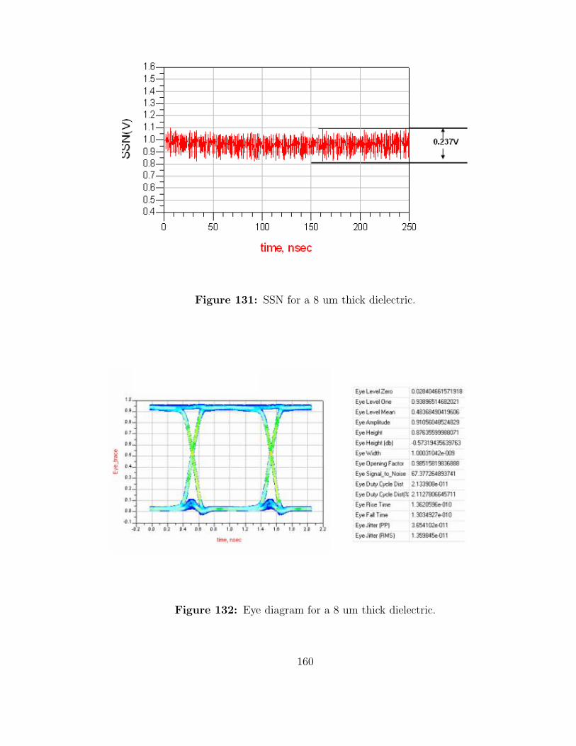
Figure 131: SSN for a 8 um thick dielectric.
Figure 132: Eye diagram for a 8 um thick dielectric.
160

Figure 133: SSN for a 12 um thick dielectric.
Figure 134: Eye diagram for a 12 um thick dielectric.
161
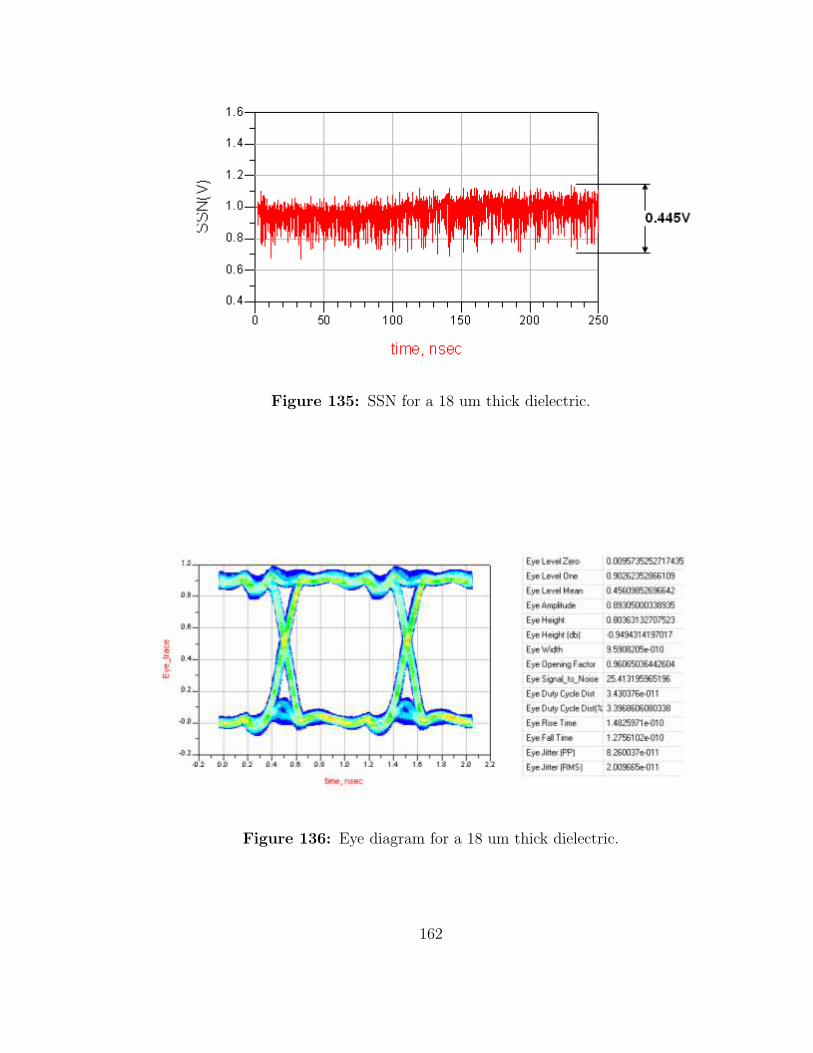
Figure 135: SSN for a 18 um thick dielectric.
Figure 136: Eye diagram for a 18 um thick dielectric.
162

Figure 137: SSN for a 25 um thick dielectric.
Figure 138: Eye diagram for a 25 um thick dielectric.
163
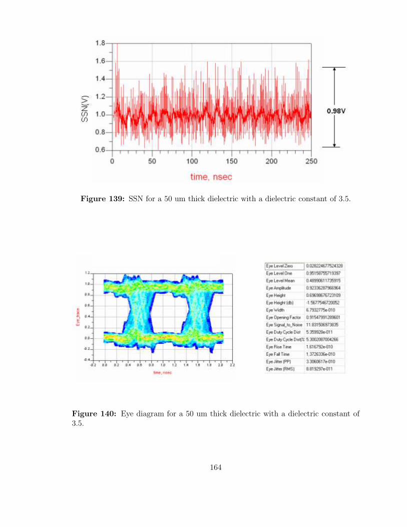
Figure 139: SSN for a 50 um thick dielectric with a dielectric constant of 3.5.
Figure 140: Eye diagram for a 50 um thick dielectric with a dielectric constant of3.5.
164
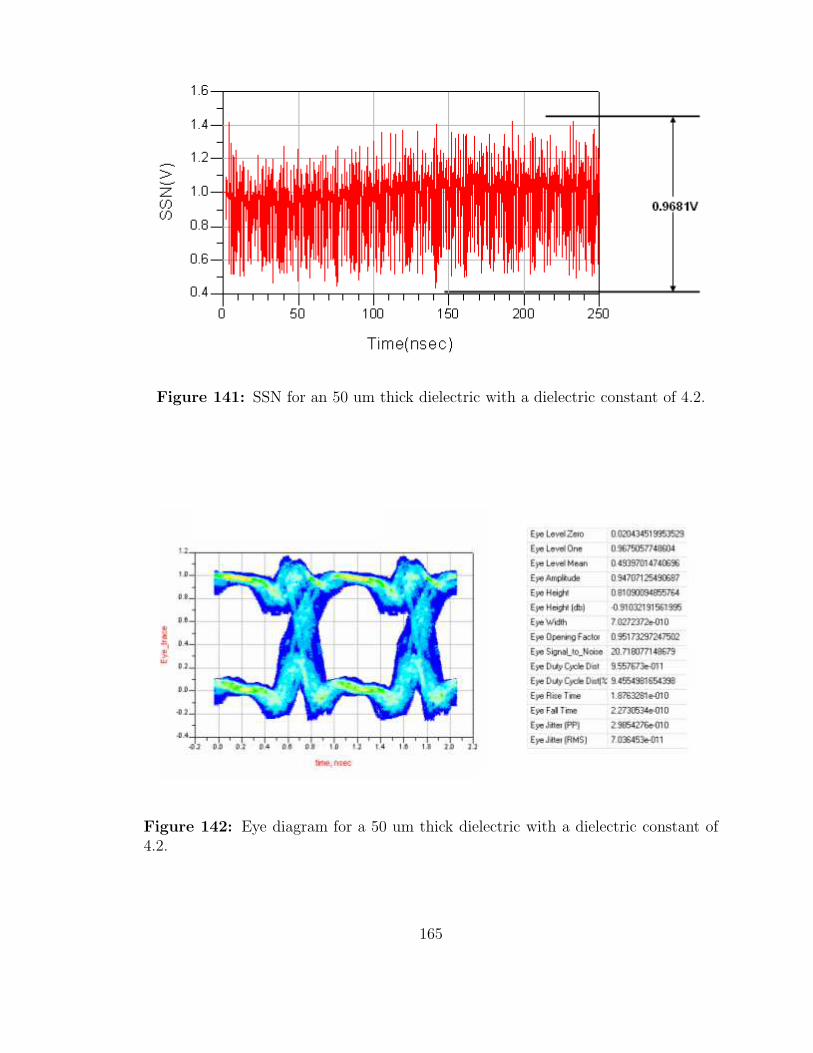
Figure 141: SSN for an 50 um thick dielectric with a dielectric constant of 4.2.
Figure 142: Eye diagram for a 50 um thick dielectric with a dielectric constant of4.2.
165

Figure 143: SSN for a 50 um thick dielectric with a dielectric constant of 3.5 with100 decoupling capacitors (C = 100 nf,ESR = 0.03Ω and ESL = 4 e-10H).
Figure 144: Eye diagram for a 50 um thick dielectric with a dielectric constant of3.5 with 100 decoupling capacitors (C = 100 nf,ESR = 0.03 Ω and ESL = 4 e-10 H).
166

APPENDIX B
SIMULATION RESULTS FOR PCI EXPRESS (PCIE) AT
5 GBIT/S
167

Figure 145: The simulation set up for the differential link simulations.
Table 17: Summary of the results for PCI Express simulations at 5 Gbit/sDielectric Thickness SSN peak to peak magnitude (mV)
8 um (HK04) 812 um (HK04) 29.418 um (HK04) 89.525 um (HK04) 128
50 um (ZBC2000) 20050 um (Nelco BC) 225
Figure 146: SSN for a differential link with a 8 um thick dielectric.
168

Figure 147: Eye diagram for a differential link with a 8 um thick dielectric.
Figure 148: SSN for a differential link with a 12 um thick dielectric.
169
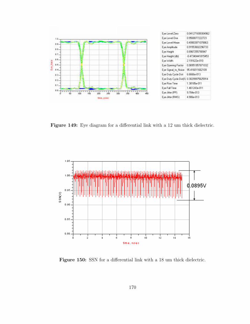
Figure 149: Eye diagram for a differential link with a 12 um thick dielectric.
Figure 150: SSN for a differential link with a 18 um thick dielectric.
170
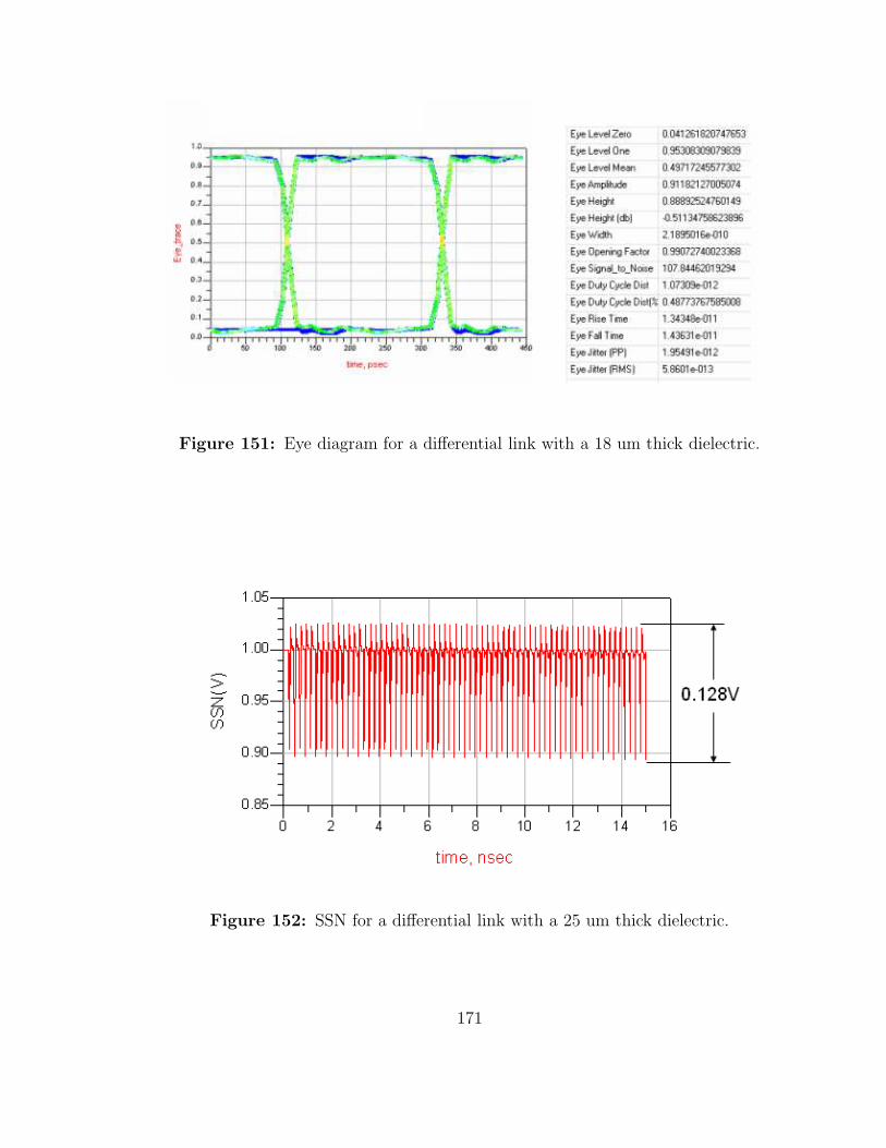
Figure 151: Eye diagram for a differential link with a 18 um thick dielectric.
Figure 152: SSN for a differential link with a 25 um thick dielectric.
171
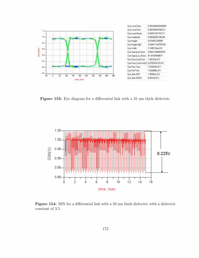
Figure 153: Eye diagram for a differential link with a 25 um thick dielectric.
Figure 154: SSN for a differential link with a 50 um thick dielectric with a dielectricconstant of 3.5.
172
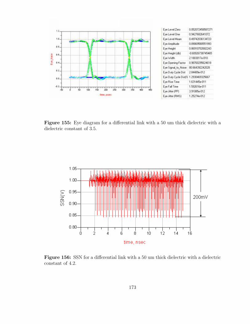
Figure 155: Eye diagram for a differential link with a 50 um thick dielectric with adielectric constant of 3.5.
Figure 156: SSN for a differential link with a 50 um thick dielectric with a dielectricconstant of 4.2.
173
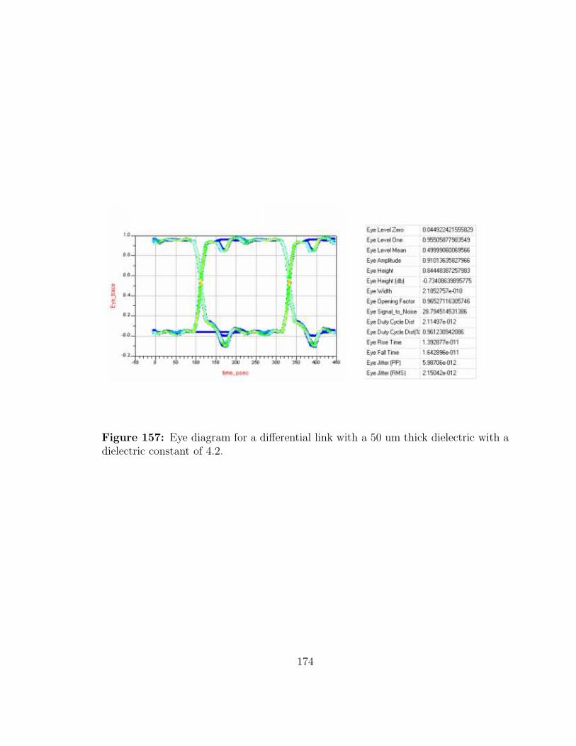
Figure 157: Eye diagram for a differential link with a 50 um thick dielectric with adielectric constant of 4.2.
174

APPENDIX C
SIMULATION RESULTS FOR PCI EXPRESS (PCIE) AT
10 GBIT/S
175

Figure 158: The simulation set up for the differential link simulations.
Table 18: Summary of the results for PCI Express simulations at 10 Gbit/sDielectric Thickness SSN peak to peak magnitude (mV)
8 um (HK04) 4412 um (HK04) 74.118 um (HK04) 106.525 um (HK04) 157
50 um (ZBC2000) 278.750 um (Nelco BC) 280
Figure 159: SSN for a differential link with a 8 um thick dielectric.
176

Figure 160: Eye diagram for a differential link with a 8 um thick dielectric.
Figure 161: SSN for a differential link with a 12 um thick dielectric.
177
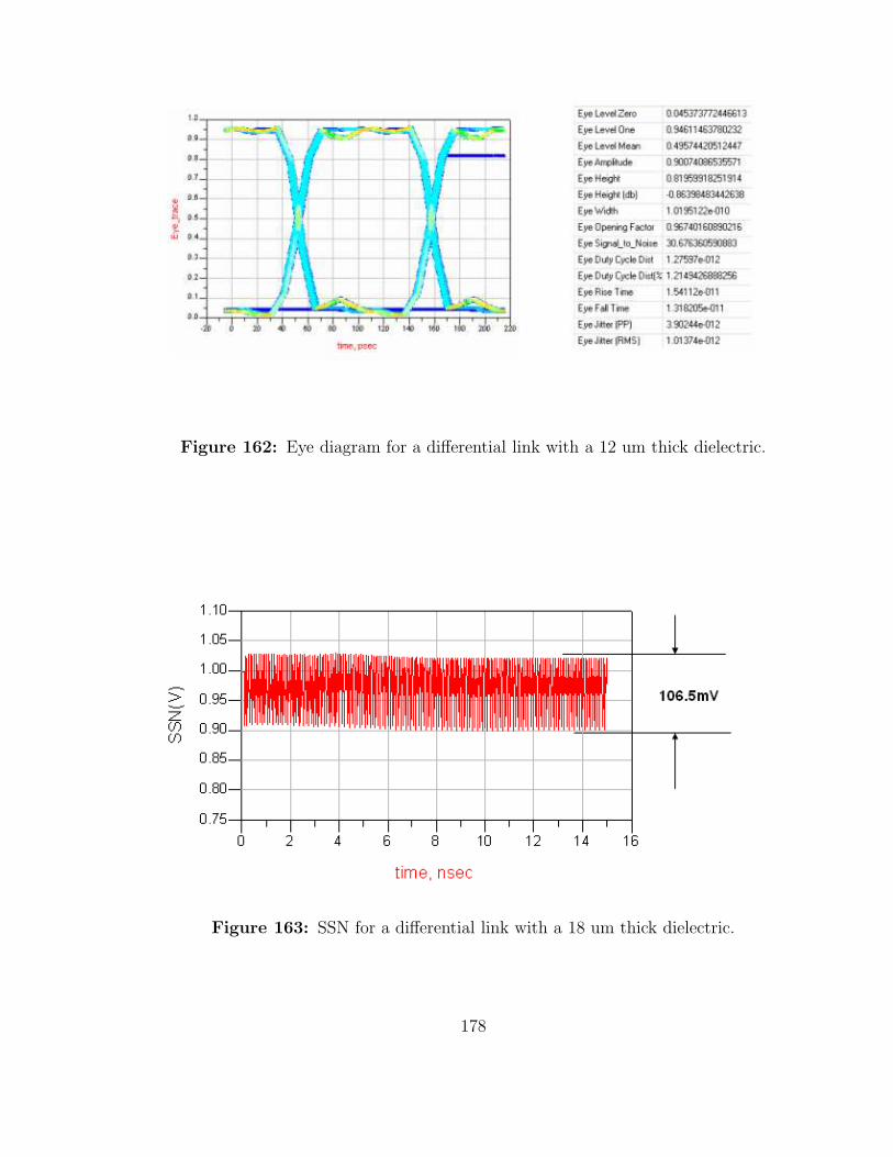
Figure 162: Eye diagram for a differential link with a 12 um thick dielectric.
Figure 163: SSN for a differential link with a 18 um thick dielectric.
178
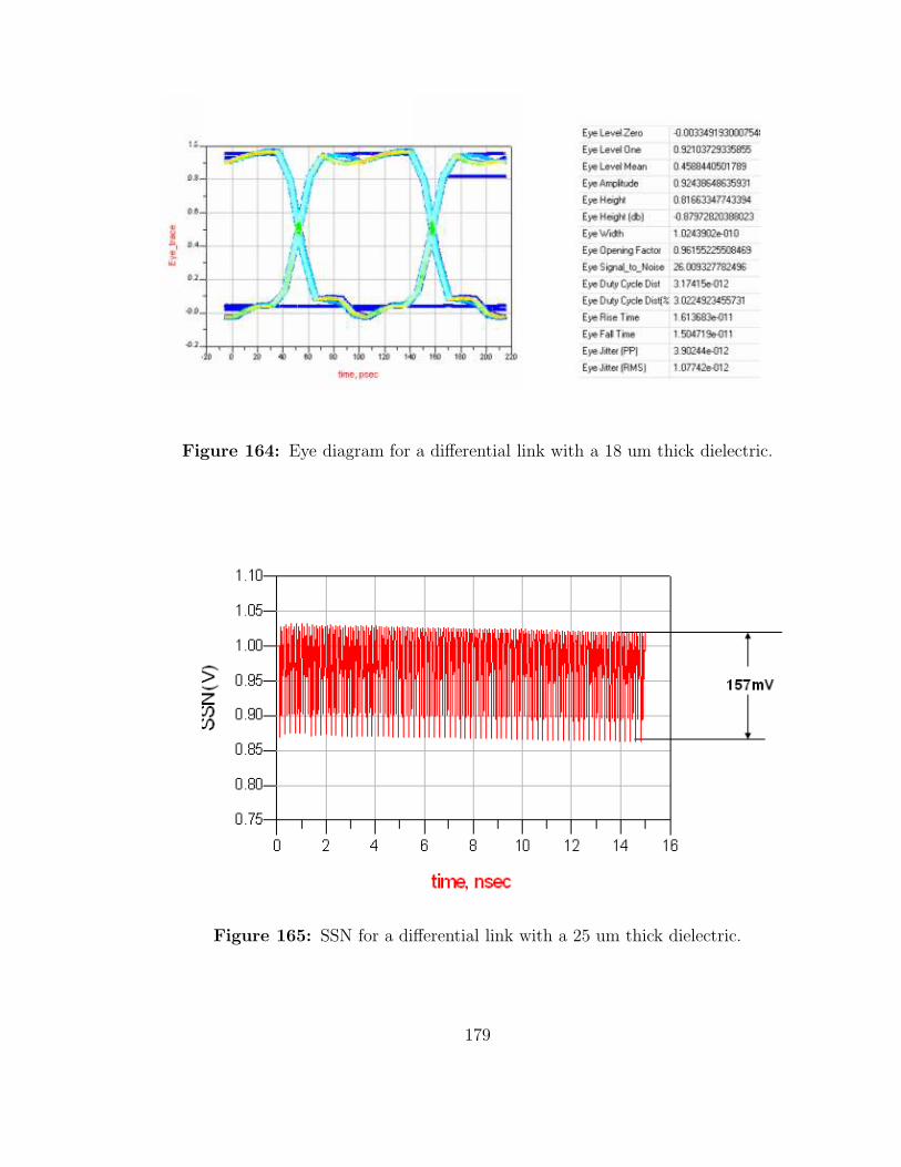
Figure 164: Eye diagram for a differential link with a 18 um thick dielectric.
Figure 165: SSN for a differential link with a 25 um thick dielectric.
179
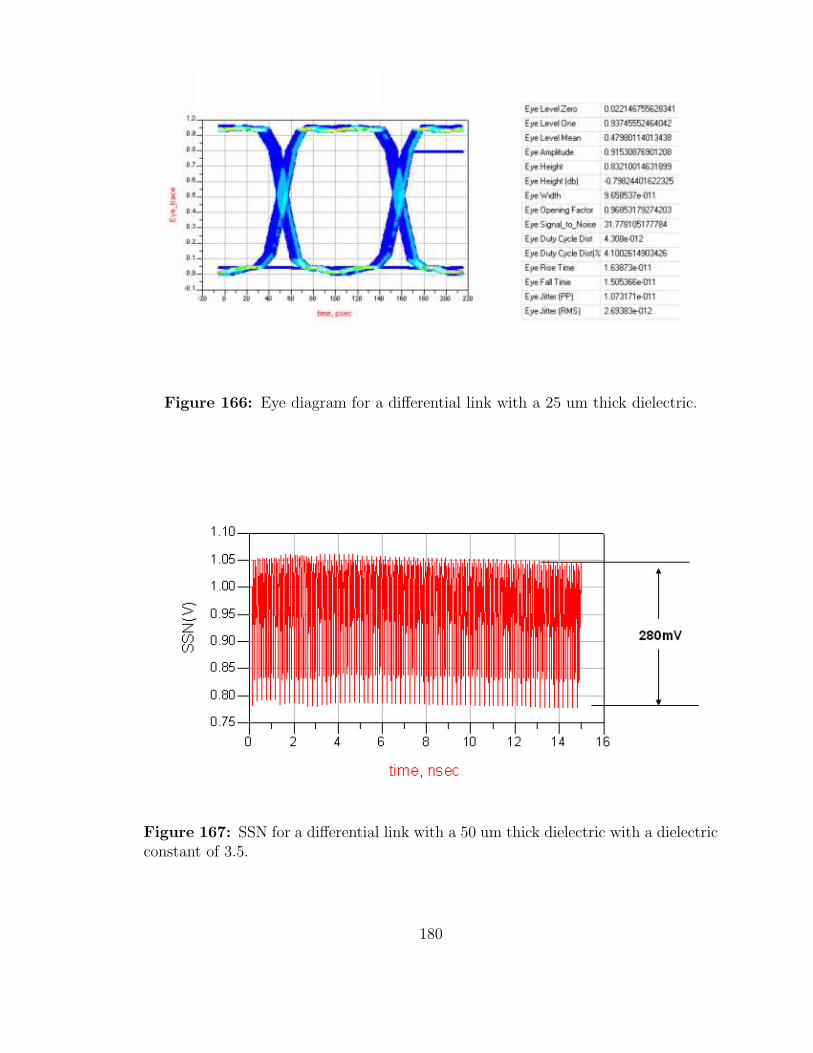
Figure 166: Eye diagram for a differential link with a 25 um thick dielectric.
Figure 167: SSN for a differential link with a 50 um thick dielectric with a dielectricconstant of 3.5.
180
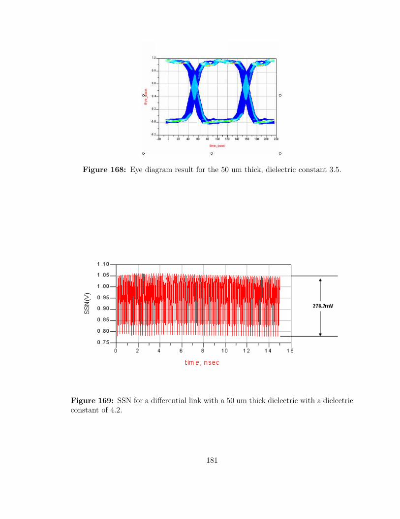
Figure 168: Eye diagram result for the 50 um thick, dielectric constant 3.5.
Figure 169: SSN for a differential link with a 50 um thick dielectric with a dielectricconstant of 4.2.
181

Figure 170: Eye diagram for a differential link with a 50 um thick dielectric with adielectric constant of 4.2.
182

REFERENCES
[1] R. Tummala, Fundamentals of Microsystems Packaging, 1st ed. McGraw Hill,
2001.
[2] “International Roadmap for Semiconductors(ITRS)- 2004 update,” Tech. Rep.,
http://public.itrs.net 03/2007.
[3] L. Smith, R. Anderson, D. Forehand, T. Pelc, and T. Roy, “Power Distribu-
tion System Design Methodology and Capacitor Selection for Modern CMOS
Technology,” IEEE Transactions on Advanced Packaging, vol. 22, no. 3, pp.
284–291, August 1999.
[4] S. Chun, “Methodologies for modeling simultaneous switching noise in multi-
layered packages and boards,” Ph.D. dissertation, Georgia Institute of Technol-
ogy, April 2002.
[5] R. Tummala, E.J.Rymaszewski, and A. Klopfenstein, Microelectronics Packag-
ing Handbook, 2nd ed. Chapman and Hall, 1997.
[6] S.Hall, G.Hall, and J.A.McCall, High-Speed Digital System Design. John Wiley
and Sons Inc, 2000.
[7] M.Shoji, High-Speed Digital Circuits. Addison-Wesley Publishing Company,
1996.
[8] J.Buchanan, Signal and Power Integrity in Digital Systems. Addison-Wesley
Publishing Company, 1996.
[9] W. D. Brown, Advanced Electronic Packaging. McGraw Hill, 1996.
183
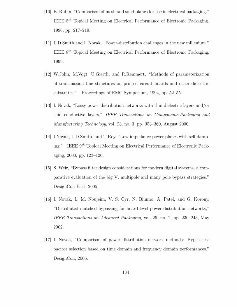
[10] B. Rubin, “Comparison of mesh and solid planes for use in electrical packaging.”
IEEE 5th Topical Meeting on Electrical Performance of Electronic Packaging,
1996, pp. 217–219.
[11] L.D.Smith and I. Novak, “Power-distribution challenges in the new millenium.”
IEEE 8th Topical Meeting on Electrical Performance of Electronic Packaging,
1999.
[12] W.John, M.Vogt, U.Gierth, and R.Remmert, “Methods of parameterization
of transmission line structures on printed circuit boards and other dielectric
substrates.” Proceedings of EMC Symposium, 1994, pp. 52–55.
[13] I. Novak, “Lossy power distribution networks with thin dielectric layers and/or
thin conductive layers,” IEEE Transactions on Components,Packaging and
Manufacturing Technology, vol. 23, no. 3, pp. 353–360, August 2000.
[14] I.Novak, L.D.Smith, and T.Roy, “Low impedance power planes with self damp-
ing.” IEEE 9th Topical Meeting on Electrical Performance of Electronic Pack-
aging, 2000, pp. 123–126.
[15] S. Weir, “Bypass filter design considerations for modern digital systems, a com-
parative evaluation of the big V, multipole and many pole bypass strategies.”
DesignCon East, 2005.
[16] I. Novak, L. M. Noujeim, V. S. Cyr, N. Biunno, A. Patel, and G. Korony,
“Distributed matched bypassing for board-level power distribution networks,”
IEEE Transactions on Advanced Packaging, vol. 25, no. 2, pp. 230–243, May
2002.
[17] I. Novak, “Comparison of power distribution network methods: Bypass ca-
pacitor selection based on time domain and frequency domain performances.”
DesignCon, 2006.
184
[18] R. Redl, B. Erisman, and Z. Zansky, “Optimizing the load transient response
of the buck converter,” vol. 1. Applied Power Electronics Conference and
Exposition, 1998, pp. 170–176.
[19] A. Waizman and C.-Y. Chung, “Resonant Free Power Netwrok Design Using
Extended Adaptive Voltage Positioning (EAVP) Methodology,” IEEE Trans-
actions on Advanced Packaging, vol. 24, no. 3, pp. 236–244, August 2001.
[20] L. D. Smith, R. Anderson, and T. Roy, “Power plane spice models and simulated
performance for materials and geometries,” IEEE Transactions on Advanced
Packaging, vol. 24, no. 3, pp. 277–287, August 2001.
[21] J. Fan, J. Drewniak, J. Knighten, N.W.Smith, A.Orlandi, T. V. Doren, T. Hub-
ing, and R. DuBroff, “Quantifying smt decoupling capacitor placement in dc
power-bus design for mulit-layer pcbs,” IEEE Transactions on Electromagnetic
Compatibility, pp. 588–599, November 2001.
[22] T. Hubing, “Effective strategies for choosing and locating printed circuit board
decoupling capacitors,” IEEE Transactions on Electromagnetic Compatibility,
vol. 2, pp. 632–637, August 2005.
[23] J.Choi, S.Chun, N.Na, M.Swaminathan, and L.Smith, “A methodology for the
placement and optimization of decoupling capacitors for gigahertz systems.”
Thirteenth International Conference on VLSI Design., 2000, pp. 156–161.
[24] “Intel flip chip pga 2000 stack-up details,” Tech. Rep.
[25] R. Ulrich, “Embedded Resistors and Capacitors for Organic-Based SOP,” IEEE
Transactions on Advanced Packaging, vol. 27, no. 2, May 2004.
185

[26] I. Novak, “Lossy Power Distribution Networks With Thin Dielectric Layers
and/or Thin Conductive Layers,” IEEE Transactions on Advanced Packaging,
vol. 23, no. 3, August 2000.
[27] H. Kim, B. K. Sun, and J. Kim, “Suppresion of GHz Range Power/Ground
Inductive and Simultaneous Switching Noise Using Embedded Film Capacitors
in Multilayer Packages and PCBs,” IEEE Microwave and Wireless Components
Letters, vol. 14, no. 2, February 2004.
[28] K.Y.Chen, W. D. Brown, L. W. Schaper, S. S. Ang, and H. A. Naseem, “A study
of high frequency performance of thin film capacitors for electronic packaging,”
IEEE Transactions on Advanced Packaging, vol. 23, no. 2, May 2000.
[29] J. S. Peiffer and W. Balliette, “Decoupling of high speed digital electronics with
embedded capacitance.” 38th International Symposium on Microelectronics,
September 2005.
[30] M.Kamon, M. Ttsuk, and J.K.White, “Fasthenry: a multipole-accelerated 3d-
inductance extraction program,” IEEE Transactions on Microwave Theory and
Techniques, vol. 42, no. 2, pp. 1750–1758, September 1994.
[31] J. H. Kim and M. Swaminathan, “Modeling of irregular shaped power dis-
tribution planes using transmission matrix method,” IEEE Transactions on
Advanced Packaging, vol. 24, no. 3, August 2001.
[32] J. G. Nickel, “Decoupling capacitance platform for substrates, sockets and in-
terposers.” DesignCon, 2005.
[33] B. Garben, G. A.Katopis, and W. D.Becker, “Package and chip design optimiza-
tion for mid-frequency power distribution decoupling.” Electrical Performance
of Electronic Packaging, 2002, pp. 245–248.
186
[34] O. P. Mandhana and J. Zhao, “Comparitive study on the effectiveness of on-
chip, on package and pcb decoupling for core noise reduction by using broad-
band power delivery network models.” Electronic Components and Technology
Conference, 2005, pp. 732–739.
[35] N. Na, T. Budell, C. Chiu, E. Tremble, and I. Wemple, “The effects of on-chip
and package decoupling capacitors and an efficient asic decoupling methodol-
ogy.” Electronic Components and Technology Conference, 2004, pp. 556–567.
[36] T. Rahal-Arabi, G. Taylor, M. Ma, J. Jones, and C. Webb, “Design and val-
idation of the core and i/o’s decoupling of the pentium R©3 and pentium R©4
processors.” Electrical Performance of Electronic Packaging, 2002, pp. 249–
252.
[37] H. Bakoglu and J. Meindl, “A system level circuit model for multi and single-
chip cpu’s.” IEEE International Solid State Circuits Conference, 1987.
[38] L. Hammond, “The case for a Single Chip Multiprocessor.” Proceedings Sev-
enth International Symposium Architectural Support for Programming Lan-
guages and Operating Systems, 1996.
[39] “Sun’s Big Splash,” Tech. Rep., iEEE Spectrum, January 2005.
[40] L. A. Barroso, K. Gharachorloo, R. McNamara, A. Nowatzyk, S. Qadeer,
B. Sano, S. Smith, R. Stets, and B. Verghese, “Piranha: A Scalable Archi-
tecture Based on Single-Chip Multiprocessing.” Proceedings of the 27 Annual
International Symposium on Computer Architecture, June 2000.
[41] H. P. Hofstee, “Future Microprocessors and Off-Chip SOP Interconnect,” IEEE
Transactions on Advanced Packaging, vol. 27, no. 2, May 2004.
187
[42] S. Borkar, “Microarchitecture and Design Challenges for Gigascale Integration,”
Tech. Rep., intel Corp,2004.
[43] A. Chandrashekar, W. Bowhill, and F. Fox, “Design of High Performance Mi-
croprocessor,” Tech. Rep., iEEE Press,2001.
[44] T. Sakurai and A. Newton, “Alpha power law MOSFET model and its appli-
cations to CMOS inverter delay and other formulas,” IEEE Journal Solid State
Circuits, vol. 25, pp. 584–593, April 1990.
[45] “The evolving topology of SOC Power Management,” Tech. Rep., virtual Silicon
Power Islands.
[46] T. Sakurai, “Closed Form Expressions for Interconnection Delay, Coupling, and
Crosstalk in VLSI’s,” IEEE Transactions on Electron Devices, vol. 40, no. 1,
January 1993.
[47] F. Pollack, New Microarchitecture Challenges in the Coming Generations of
CMOS Process Technologies. Micro, 1999.
[48] P. Gelsinger, “Microprocessors for the new millenium : Challenges, opportuni-
ties and new frontiers.” IEEE International Solid State Circuits Conference,
2001.
[49] D.Burger, J.R.Goodman, and A.Kagi, “Memory bandwidth limitations of fu-
ture microprocessors.” 23rd International Symposium on Computer Architec-
ture, May 1996.
[50] W. Kim, “Development of measurement-based time domain models and its
application to wafer level packaging,” Ph.D. dissertation, Georgia Institute of
Technology, 2004.
188

[51] F. Liu, G. White, V. Sundaram, A. Aggarwal, S. Hosseini, D. Sutter, and
R. Tummala, “A novel technology for stacking microvias on printed wiring
boards.” Electronic Components and Technology Conference, May 2003, pp.
1134–1139.
[52] D. Balaraman, “BaTiO3 films by low-temperature hydrothermal techniques for
next generation packaging applications,” Journal of Electroceramics, vol. 13,
pp. 950–100, 2004.
[53] W. Borland, M. Doyle, L. Dellis, O. Renovales, and D. Majumdar, “Embedding
ceramic thick-film capacitors into printed wiring boards,” Materials Research
Socitey Symposium Proceedings, vol. 833, pp. 143–152, 2005.
[54] I. Novak and J. R. Miller, “Frequency dependent characterization of bulk and
ceramic bypass capacitors.” Poster Material for the 12th Topical Meeting on
Electrical Performance of Electronic Packaging, October 2003, pp. 101–104.
[55] D. Pozar, Microwave Engineering. John Wiley and Sons, 2005.
[56] I. Novak, “Measuring milliohms and picohenrys in power-distribution net-
works.” DesignCon, 2000.
[57] J. Choi, S.-H. Min, J.-H. Kim, B. W. Madhavan Swaminathan, and X. Yuan,
“Modeling and analysis of power distribution networks for gigabit applications,”
IEEE Transactions on Advanced Packaging, vol. 2, pp. 299–313, October-
December 2003.
[58] C. Y. Beyene W, J. H. Kim, and M. Swaminathan, “Modeling and analysis
of power distribution networks for gigabit applications.” Proceedings of the
Fourth International Symposium on Quality Electronic Design(ISQED), 2003,
pp. 235–240.
189
[59] Tech. Rep., www.ansoft.com 03/2007.
[60] Tech. Rep., www.sigrity.com 03/2007.
[61] Tech. Rep., www.sonnetusa.com 03/2007.
[62] P. Muthana, M. Swaminathan, R. Tummala, P.M.Raj, E. Engin, L. Wan,
D.Balaraman, and S.Bhattacharya, “Design, modeling and characterization of
embedded capacitors for mid-frequency decoupling in semiconductor systems.”
Electromagnetic Compatibility, 2005, pp. 638–643.
[63] P. Muthana, M. Swaminathan, E. Engin, P.M.Raj, and R. Tummala, “Mid-
frequency decoupling using embedded decoupling capacitors.” Electrical Per-
formance of Electronic Packaging, 2005, pp. 271–275.
[64] N.Pham, M.Cases, D. de Araujo, B.Mutnury, E. Matoglu, B.Herrman, and
P.Patel, “Embedded capacitor in power distribution design of high-end server
packages.” Electronic Components and Technology Conference, 2006.
[65] N.Pham, M.Cases, D. de Araujo, B.Mutnury, E. Matoglu, and M.Swaminathan,
“Design and modeling methodology for high performance power distribution
systems.” DesignCon, 2002.
[66] V.Sundaram, R.Tummala, B.Weidenman, F.Liu, PM.Raj, R.Abothu,
S.Bhattacharya, M.Swaminathan, E.Bongio, and W.Sherwood, “Recent ad-
vances in low cte and and high system on a package subsrate with thin film
component.” Electronic Component and Technology Conference, 2006, pp.
1375–1380.
[67] “https://www.avx.com/ 03/2007,” Tech. Rep.
[68] J. Sisler, “Eliminating capacitors from multilayer pcbs,” Tech. Rep., printed
Circute Design, Vol8, No.7, July 1991.
190
[69] C.Chang and A.Agrawal, “Fine line thin dielectric circuit board characteri-
zation.” IEEE Transactions on Components, Packaging, and Manufacturing
Technology, vol. 18, no. 4, pp. 842–850, Decemeber 1995.
[70] T. Hubing, “Power bus decoupling on multilayer printed circuit boards,” IEEE
Transactions on Electromagnetic Compatibility, vol. 37, May 1995.
[71] H. Kim, Y.Jeong, J.Park, S.Lee, J.Hong, Y.Hong, and J.Kim, “Significant re-
duction of power/ground inductive impedance and simultaneous switching noise
by using embedded film capacitor.” Electronic Performance of Electronic Pack-
aging, October 2003, pp. 129–132.
[72] J. Grebenkemper, “The effects of thin laminates on signal integrity,” Tech. Rep.,
PC FAB, November. 2002, pp38-41.
[73] C. Guiles, “Everything you wanted to know about laminates for frequency de-
pendent applications part 1,” Tech. Rep., circuitree, January 2002, pp 58-68.
[74] ——, “Everything you wanted to know about laminates for frequency dependent
applications part 2,” Tech. Rep., circuitree, January 2002, pp 42-50.
[75] T. McCarthy, “PTFE-based composites for high-speed digital designs,” Tech.
Rep., pC FAB, August 2002, pp36-41.
[76] E. Bogatin, “Materials requirements for high performance digital systems,”
Tech. Rep., circuitree, August 2003, pp34-39.
[77] T. Yamamoto, “Non-reinforced substrates for use as embedded capacitors,”
Tech. Rep., printed Circuit Design And Manufacture, April 2003, pp36-40.
191

[78] J. Peiffer, B. Greenlee, and I. Novak, “Electrical performance advantages of
ultra-thin dielectric materials used for power-ground cores in high speed, mul-
tilayer printed circuit board.” IPC Printed Circuits Expo, 2003, pp. S15–4–1
to S15–4–11.
[79] J. Peiffer, “Ultra-thin loaded epoxy materials for use as embedded capacitor
layers,” Tech. Rep., printed Circuit Design And Manufacture, April 2004, pp
40-42.
[80] D. Mcgregor, “Recent developments in polyimide-based planar capacitor lami-
nates.” IPC/FED Conference on Embedded Passives, 2004.
[81] N. Biunno and G. Schroder, “Buried capacitance and thin laminates,” Tech.
Rep., circuitree, March 2004, pp 42-48.
[82] B. Balliette, “Ultra-thin, loaded epoxy materials for use as embedded capaci-
tor layers / thin and very thin laminates for power distribution applications.”
TecForum TF9 / DesignCon, August 2004, pp. 11–18.
[83] J. Andresakis, “Performance of polymeric ultra-thin substrates for use as em-
bedded capacitors: Comparison of unfilled and filled systems with ferroelectric
particles / thin and very thin laminates for power distribution applications.”
TecForum TF9 / DesignCon, August 2004, pp. 19–24.
[84] B. Greenlee, “Processing thin and very thin laminates: What is new in 2004 /
thin and very thin laminates for power distribution applications.” TecForum
TF9 / DesignCon, August 2004, pp. 26–29.
[85] L. Riley, “Processing thin and very thin laminates: Unicircuits experience /
thin and very thin laminates for power distribution applications.” TecForum
TF9 / DesignCon, August 2004, pp. 30–31.
192

[86] ——, “Benchmarks experience with thin laminates / thin and very thin lami-
nates for power distribution applications.” TecForum TF9 / DesignCon, Au-
gust 2004, pp. 32–34.
[87] J. Grebenkemper, “Thin laminates and power plane noise / thin and very thin
laminates for power distribution applications.” TecForum TF9 / DesignCon,
August 2004, pp. 35–38.
[88] I. Novak, “Frequency dependent capacitance and inductance of thin and very
thin laminates / thin and very thin laminates for power distribution applica-
tions.” TecForum TF9 / DesignCon, August 2004, pp. 39–47.
[89] D. Leys, “Best materials for 3-6 ghz design,” Tech. Rep., printed Circuit Design
And Manufacture, November 2004, pp34-39.
[90] J. Andresakis, “Common mode radiation of a printed circuit board with embed-
ded decoupling capacitor excited by ics shoot-through current.” DesignCon,
2007.
[91] J. Peiffer, “Using embedded capacitance to improve electrical performance,
eliminate capacitors and reduce board size in high speed digital and rf ap-
plications.” IPC APEX, 2007.
[92] A. Engin, W. John, G. Sommer, W. Mathis, and H. Reichl, “Modeling of
striplines between a power and ground plane.” IEEE Transactions on Advanced
Packaging, vol. 29, no. 3, August 2006.
[93] X.Wang, S.Kabir, J.Weber, S.Dvorak, and J.Prince, “A study of the fields asso-
ciated with horizontal dipoles sources in stripline circuits.” IEEE Transactions
on Advanced Packaging, vol. 25, no. 2, pp. 280–287, May 2002.
193

[94] M.Burchett, S.Pennock, and P.Shepherd, “A rigorous analysis of uniform
stripline of arbitrary dimensions.” IEEE Transactions on Microwave Theory
Technology, vol. 41, no. 12, pp. 2074–2080, December 1993.
[95] C.R.Paul, Analysis of Multiconductor Transmission Lines. John Wiley and
Sons, 1994.
[96] D. Hockanson, X.Ye, J.Drewniak, T.Hubing, T. Doren, and R.DuBroff, “Power
bus decoupling on multilayer printed circuit boards.” IEEE Transactions on
Electromagnetic Compatibility, vol. 43, no. 1, February 2001.
[97] H. Kim, H. Park, Y.Jeong, and J.Kim, “High dielectric constant thin film em-
bedded capacitor for suppression of simultaneous switching noise and radiated
emissions.” International Symposium on Electromagnetic Compatibility, Au-
gust 2004, pp. 588–591.
[98] F.Yang, K.Ma, Y.Qian, and T.Itoh, “A unipolar compact photonic bandgap
(uc-ebg) structure and its applications for microwave circuits.” IEEE Transac-
tions on Microwave Theory Technology, vol. 47, August 1999.
[99] Z.N.Chen, N.Yang, Y.Y.Yang, and M.Y.W.Chia, “A novel electromagnetic
bandgap structure and its application for antenna duplexer.” vol. 71-74. IEEE
Radio Wireless Conference, September 2002.
[100] T.Kamgaing and O.Ramahi, “High impedance electromagnetic surfaces for par-
allel plate mode suppression in high speed systems.” vol. 279-282. Electrical
Performance of Electronic Packages, October 2002.
[101] R.Abhari and G.V.Eleftheriades, “Metallo-dielectric electromagnetic bandgap
structures for suppression and isolation of parallel plate noise in high speed
circuits.” IEEE Transactions on Microwave Theory Technology, vol. 51, pp.
1629–1639, June 2003.
194
[102] D.Sievenpiper, L.Zhang, R.Broas, N.Alexopolous, and E.Yablonovitch, “High
impedance electromagnetic surface with a forbidden frequency band.” IEEE
Transactions on Microwave Theory Technology, vol. 47, November 1999.
[103] J.Choi, V.Govind, M.Swaminathan, L.Wan, and R.Doraiswami, “Isolation in
mixed-signal systems using a novel electromagentic band-gap(ebg) structure.”
vol. 199-202. Electrical Performance of Electronic Packages, October 2004.
[104] S. D. Rogers, “Electromagnetic -bandgap layers for broad-band suppression of
tem modes in power planes.” IEEE Transactions on Microwave Theory and
Techniques, vol. 53, no. 8, pp. 2495–2505, August 2005.
195