design of novel mimo-ofdm using random ... - … · at the transmitter and receiver to increase the...
TRANSCRIPT
International Journal of Recent Development in Engineering and Technology
Website: www.ijrdet.com (ISSN 2347 - 6435 (Online)), Volume 2, Special Issue 3, February 2014)
International Conference on Trends in Mechanical,Aeronautical,Computer,Civil,Electrical and Electronics Engineering
(ICMACE14)
Tamizhan College of Engineering and Technology (ISO 9001:2008 Certified Institution),Tamilnadu,INDIA Page 157
DESIGN OF NOVEL MIMO-OFDM USING RANDOM INTERLEAVER FOR 4G
WIRELESS COMMUNICATION
G.Gangaram, MR.N.Muthu sankar M.E,
ECE Department Asst. Prof, Dept. of ECE
Sri Muthukumaran Institute Of Technolog
Chennai, Tamil nadu, India
Abstract – Orthogonal frequency division multiplexing
(OFDM) is a popular method for high data rate wireless
transmission. OFDM may be merged with antenna arrays
at the transmitter and receiver to increase the diversity
gain and/or to heighten the system capacity on time-
variant and frequency-selective channels, resulting in a
multiple-input multiple-output (MIMO) configuration.
The FFT/IFFT processor is one of the highest
computational complexity modules in the physical layer of
the IEEE 802.11n standard. This paper proposed to the
improve the signal processing capability and to reduce the
power consumption as well as the hardware cost of a FFT
processor have now all become challenging targets. In this
paper present a pipelined Fourier transform (FFT)/
inverse FFT (IFFT) processor for the applications in a
multiple-input multiple-output orthogonal frequency-
division multiplexing based IEEE 802.11n wireless local
area network baseband processor. High throughput,
memory reduction, low power, complex multiplier
reduction are achieved by using radix-2 based FFT
algorithm in MIMO-OFDM. The radix-2 with bit reversal
FFT architecture is proposed to efficiently deal with data
sequences. Furthermore, the power consumption can also
be saved by using MIMO_OFDM architecture with radix-
2 based FFT algorithm with minimal hardware
complexity.
Index Terms — Pipelined FFT/IFFT, MIMO-OFDM.
I.INTRODUCTION
High data rate wireless communication has improved by
a factor of minimum four while migrating from one
generation to next generation . The technology is based on
Orthogonal Frequency Division Multiplexing (OFDM).
The upcoming standard 802.11n WLAN, however, can
achieve 250 Mbits/s by virtue of Multiple Input Multiple
Output OFDM (MIMO-OFDM) technology. This on going
evolution has accelerated the development of system-on-chip
(SoC) platforms to support the physical layer of those
technologies [3].The SoC platforms must satisfy two
requirements in order to support this wireless technology.
Wireless communication is VLSI Design and Implementation
of MIMO-OFDM System for Wireless Communications 270
obviously less reliable than wired communication. For
example, the IEEE standard 802.11a [1] has various
communication modes with possible data rates of 6, 9, 12, 18,
24, 36, 48, and 54 Mbits/s. To implement the OFDM or
MIMO-OFDM physical layer on a SoC, many efforts have
been carried out by DSP, VLSI, FPGA, and communication
groups. In optimized DSP implementation of an OFDM
transmitter was developed. Application specific integrated
circuit (ASIC) chips and test-beds for MIMO-OFDM were
proposed. In , a prototype field programmable gate array
(FPGA) implementation of an OFDM physical layer is shown
using the Xilinx System Generator. Advantage Of MIMO-
OFDM is Less interference, Diversity gain, Increase data
capacity, Power efficiency, Bandwidth gain.
Both studies use FPGA intellectual property components (IP
Cores), and libraries to build most of the kernels. An OFDM
wireless transceiver for 802.16 Wi-MAX (Broadband
Wireless Access Technology), using Lattice FPGA and IP
Cores is described in. A test-bed for MIMO-OFDM using
FPGA transceivers and their customized hardware boards is
developed in . This test-bed is built using Vertex-II transceiver
boards. The benefit of reconfigurable architecture for wireless
communication is discussed, and its potential is explored
through prototyping . The 802.11n and the 802.16e standards
for MIMO-OFDM have not yet been established.
International Journal of Recent Development in Engineering and Technology
Website: www.ijrdet.com (ISSN 2347 - 6435 (Online)), Volume 2, Special Issue 3, February 2014)
International Conference on Trends in Mechanical,Aeronautical,Computer,Civil,Electrical and Electronics Engineering
(ICMACE14)
Tamizhan College of Engineering and Technology (ISO 9001:2008 Certified Institution),Tamilnadu,INDIA Page 158
The input and output data rates shown in these figures are
based on our assumptions. We assume that the data rate of
MIMO-OFDM is N times that of OFDM, if we use N
antennas in both the transmitter and the receiver. In the case of
the OFDM standard, 20 Mega symbols per second are
required. The paper is organized as follows. Section II
presents an overview of the MIMO-OFDM system. Section III
discusses the simulation results Section IV presents the
implementation of the whole MIMO-OFDM transmitter, and
puts an emphasis on an innovative design of the convolution
encoder and BPSK modulator Section V results and
discussions and concludes the paper.
II. FFT AND IFFT IN OFDM
The orthogonal frequency division multiplexing
(OFDM) system is a form of multicarrier modulation (MCM)
technology. OFDM is bandwidth efficient multiple access
schemes for digital communication system.FFT/IFFT
processor is an critical block of an OFDM system. It performs
multicarrier baseband modulation and demodulation .Chip
area of the processor is an important factor that occupies large
part in OFDM transceiver. In this proposal we can implement
High throughput OFDM Transceiver using efficient FFT
Algorithm.
OFDM is implemented in broadband wireless access systems
as a way to overcome wireless channel impairments. OFDM is
used today in wireless local area network (LANs) as specified
by the IEEE 802.11a.It is also used for wireless digital radio
and television transmissions. OFDM transceivers make use of
direct computation of DFT and IDFT that involves complex
multipliers and adders since this method does not involve
periodicity property of twiddle factor. It increases the
hardware complexity and power optimization is not easily
achieved.
III. MIMO-OFDM USING RADIX-2 ALGORITHM
The proposed system aims to achieve high data rates, speed
and simultaneous increase in range and reliability without
consuming extra radio frequency requires MIMO-OFDM for
wireless broadband communication. In this paper first we
integrate OFDM to MIMO.
In this method, the development of 64 point FFT, based on
Decimation-In- Time (DIT) domain using Radix- 2 algorithm
and MIMO-OFDM Communication System. This paper
investigates the performance of MIMO-OFDM using BPSK
modulation used to encode and decode the data stream in
wireless communication over AWGN channel for unknown
transmitter and known receiver. The results confirm the speed
and area advantages for large FFTs. Although only radix-2
FFT address generation is presented in the paper, it can be
used for higher radix FFT.
A FPGA parameters also we will find such that
AREA (Slices), Delay (ns) and Frequency (MHz) .Cost
efficient, multiplier less IFFT/FFT processor with its fixed
point error analysis is designed. This processor employs
radix2 algorithm. Proposed classification of twiddle factor and
hardware sharing are used to minimize non zero bits of the
shift and the add operation. This architecture achieve to
maximum frequency 133.025MHZ and clock minimum period
7.517 For Test Vehicle IEEE802.16a MIMO-OFDM system.
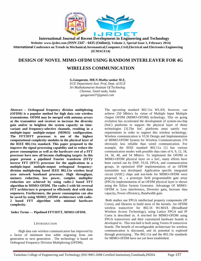
MIMO-OFDM system is shown in fig 1 .
Fig. 1. Q x L MIMO-OFDM system, where Q and L are
the numbers of inputs and outputs, respectively.
IV.SYSTEM DESCRIPTION
The basic architecture of the OFDM communication system
is shown in Fig. 1. The FEC blocks include convolutional
encoding with radix-2 algorithm As shown in Figure the input
serial binary data will be processed by a data scrambler first
and then channel coding is applied to the input data to
improve the BER (bit error rate) performance of the system.
The encoded data stream is further interleaved to reduce the
burst symbol error rate. Dependent on the channel condition
like fading, different base modulation modes such as BPSK
(binary phase shift keying),
International Journal of Recent Development in Engineering and Technology
Website: www.ijrdet.com (ISSN 2347 - 6435 (Online)), Volume 2, Special Issue 3, February 2014)
International Conference on Trends in Mechanical,Aeronautical,Computer,Civil,Electrical and Electronics Engineering
(ICMACE14)
Tamizhan College of Engineering and Technology (ISO 9001:2008 Certified Institution),Tamilnadu,INDIA Page 159
QPSK (quadrature phase shift keying) and QAM are
adaptively used to boost the data rate. The modulation mode
can be changed even during the transmission of data frames.
The resulting complex numbers are grouped into column
vectors which have the same number of elements as the FFT
size, N. For simplicity of presentation and ease of
understanding, we choose to use matrix and vector to describe
the mathematical model. Let S(m) represent the m-th OFDM
symbol in the frequency domain,
i.e.
,
where m is the index of OFDM symbols. We assume that the
complex-valued elements consist of {S(mN); S(mN + 1),……,
S(mN + N -1)} of S (m) are zero mean and uncorrelated
random variables whose sample space is the signal
constellation of the base modulation (BPSK, QPSK and
QAM).
To achieve the same average power for all different
mappings, a normalization factor is multiplied to each
elements of S (m) such that the average power of the different
mappings is normalized to unity. To obtain the time domain
samples, as shown by the IDFT block in Figure, an IFFT
(inverse fast Fourier transform) operation is represented by a
matrix multiplication.
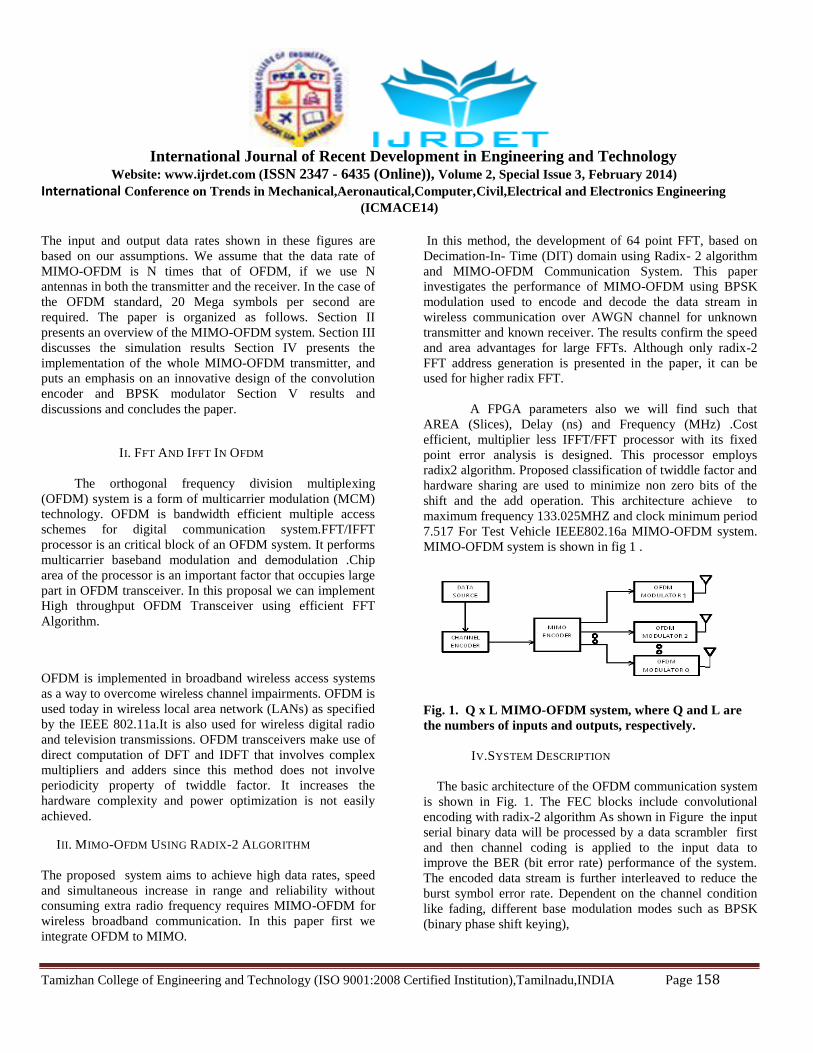
V.BLOCK DIAGRAM
1.OFDM communication system
Let FN be the N-point DFT matrix whose (p,q)-th elements is
the resulting time domain samples s(m) can be described by
S=(1/N)FHNS(m)
Compared to the costly and complicated modulation and
multiplexing of conventional FDM systems, OFDM systems
easily implement them by using FFT in baseband processing.
To combat the multipath delay spread in wireless channels,
the time-domain samples s(m) is cyclically extended by
copying the last Ng samples and pasting them to the front, as
shown in Figure
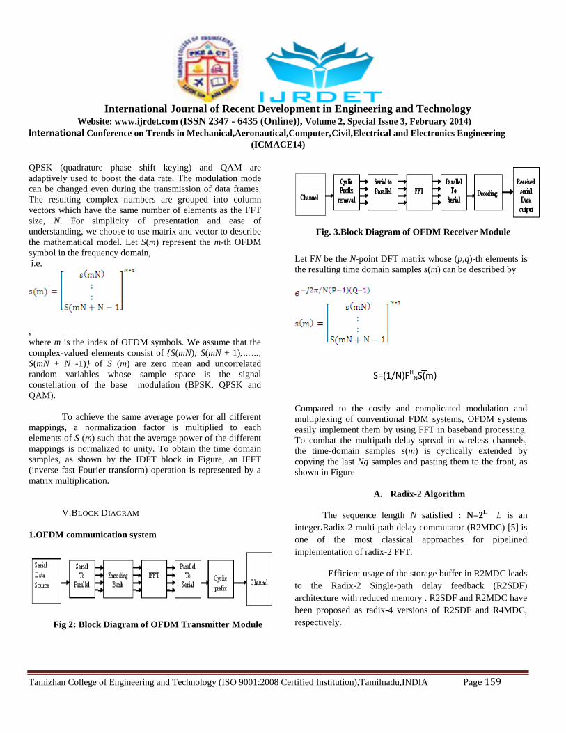
A. Radix-2 Algorithm
The sequence length N satisfied : N=2L
L is an
integer.Radix-2 multi-path delay commutator (R2MDC) [5] is
one of the most classical approaches for pipelined
implementation of radix-2 FFT.
Efficient usage of the storage buffer in R2MDC leads
to the Radix-2 Single-path delay feedback (R2SDF)
architecture with reduced memory . R2SDF and R2MDC have
been proposed as radix-4 versions of R2SDF and R4MDC,
respectively. Fig 2: Block Diagram of OFDM Transmitter Module
Fig. 3.Block Diagram of OFDM Receiver Module
International Journal of Recent Development in Engineering and Technology
Website: www.ijrdet.com (ISSN 2347 - 6435 (Online)), Volume 2, Special Issue 3, February 2014)
International Conference on Trends in Mechanical,Aeronautical,Computer,Civil,Electrical and Electronics Engineering
(ICMACE14)
Tamizhan College of Engineering and Technology (ISO 9001:2008 Certified Institution),Tamilnadu,INDIA Page 160
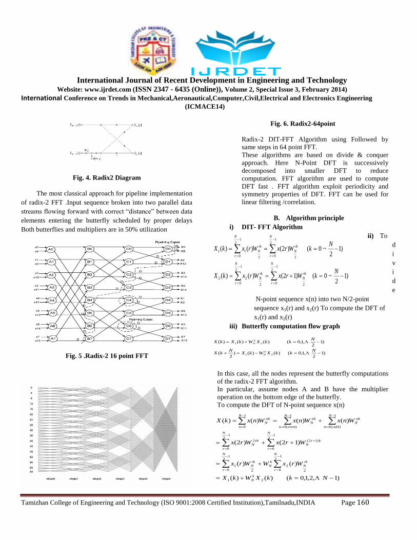
Fig. 4. Radix2 Diagram
The most classical approach for pipeline implementation
of radix-2 FFT .Input sequence broken into two parallel data
streams flowing forward with correct “distance” between data
elements entering the butterfly scheduled by proper delays
Both butterflies and multipliers are in 50% utilization
Fig. 5 .Radix-2 16 point FFT
Fig. 6. Radix2-64point
Radix-2 DIT-FFT Algorithm using Followed by
same steps in 64 point FFT.
These algorithms are based on divide & conquer
approach. Here N-Point DFT is successively
decomposed into smaller DFT to reduce
computation. FFT algorithm are used to compute
DFT fast . FFT algorithm exploit periodicity and
symmetry properties of DFT. FFT can be used for
linear filtering /correlation.
B. Algorithm principle
i) DIT- FFT Algorithm
ii) To
d
i
v
i
d
e
N-point sequence x(n) into two N/2-point
sequence x1(r) and x2(r) To compute the DFT of
x1(r) and x2(r)
iii) Butterfly computation flow graph
In this case, all the nodes represent the butterfly computations
of the radix-2 FFT algorithm.
In particular, assume nodes A and B have the multiplier
operation on the bottom edge of the butterfly.
To compute the DFT of N-point sequence x(n)
)12
~0( )12()()(
)12
~0( )2()()(
12
0 2
12
0 2
22
12
0 2
12
0 2
11
NkWrxWrxkX
NkWrxWrxkX
N
r
rk
N
N
r
rk
N
N
r
rk
N
N
r
rk
N
)12
,1,0( )()()2
(
)12
,1,0( )()()(
21
21
NkkXWkX
NkX
NkkXWkXkX
k
N
k
N
)1,2,1,0( )()(
)()(
)12()2(
)()()()(
21
12
0 2
2
12
0 2
1
12
0
)12(
12
0
2
1
)(0
1
)(0
1
0
NkkXWkX
WrxWWrx
WrxWrx
WnxWnxWnxkX
k
N
N
r
rk
N
k
N
N
r
rk
N
N
r
kr
N
N
r
rk
N
N
oddn
nk
N
N
evenn
nk
N
N
n
nk
N
International Journal of Recent Development in Engineering and Technology
Website: www.ijrdet.com (ISSN 2347 - 6435 (Online)), Volume 2, Special Issue 3, February 2014)
International Conference on Trends in Mechanical,Aeronautical,Computer,Civil,Electrical and Electronics Engineering
(ICMACE14)
Tamizhan College of Engineering and Technology (ISO 9001:2008 Certified Institution),Tamilnadu,INDIA Page 161
The N-point discrete Fourier transform is defined by
where k=0,1,2,…N-1
The N-point FFT can be decomposed to repeated micro
operations called butterfly operations. [6]When the size of the
butterfly is r, the FFT operation is called a radix-r FFT. For
FFT hardware realization, if only one butterfly structure is
implemented in the chip, this butterfly unit will execute all the
calculations recursively. If parallel and pipeline processing
techniques are used, an N point radix-r FFT can be executed
by N/(r log N) clock cycles. This indicates that a radix-4 FFT
can be four times faster than a radix-2 FFT. Fig 6 shows a
diagram for an 64-point radix-2 DIT-FFT (decimation in time-
FFT). There are several ways to calculate a radix-2 FFT
because the derivation from the DFT can be performed
differently. Finally, we end up with the distinction of
decimation in time and decimation in frequency, depending on
how the twiddle factors are arranged in the butterfly. In
addition, we can have bit-reversed inputs or outputs. The
scrambling caused by the bit-reversal can be corrected in the
first or the last stage of the FFT.
C. Bit Reversal
Bit reversal is necessary to reorder the results or
respectively the input data. Discrete transforms are the main
users of bit-reverse and digit-reverse routines. Discrete
transforms take discrete inputs in one domain and convert
them to discrete outputs in another.
For example, an FFT takes a discrete time domain input and
transforms it into the discrete frequency domain output (i.e.,
x(t) X(jwt).) Bit-reverse and digit-reverse routines are routines
in which the data is reordered based on its index value from 0
to –1, where N is the number of points to be bit-reversed.
VI. SYSTEM IMPLEMENTATION
To analyze the hardware implication of various coding and
interleaving schemes considered in this paper, in this section,
the IEEE 802.16-2009 (WiMAX) transmitter is modeled in
VHDL and implemented on an FPGA platform. However,
before presenting the details of the implementation, a brief
presentation of the existing trends in MIMO-OFDM systems
implementation is in order of interleaving concept.
.
A. Convolutional Encoder
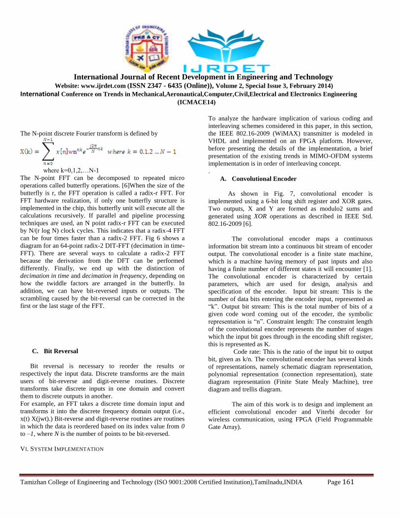
As shown in Fig. 7, convolutional encoder is
implemented using a 6-bit long shift register and XOR gates.
Two outputs, X and Y are formed as modulo2 sums and
generated using XOR operations as described in IEEE Std.
802.16-2009 [6].
The convolutional encoder maps a continuous
information bit stream into a continuous bit stream of encoder
output. The convolutional encoder is a finite state machine,
which is a machine having memory of past inputs and also
having a finite number of different states it will encounter [1].
The convolutional encoder is characterized by certain
parameters, which are used for design, analysis and
specification of the encoder. Input bit stream: This is the
number of data bits entering the encoder input, represented as
“k”. Output bit stream: This is the total number of bits of a
given code word coming out of the encoder, the symbolic
representation is “n”. Constraint length: The constraint length
of the convolutional encoder represents the number of stages
which the input bit goes through in the encoding shift register,
this is represented as K.
Code rate: This is the ratio of the input bit to output
bit, given as k/n. The convolutional encoder has several kinds
of representations, namely schematic diagram representation,
polynomial representation (connection representation), state
diagram representation (Finite State Mealy Machine), tree
diagram and trellis diagram.
The aim of this work is to design and implement an
efficient convolutional encoder and Viterbi decoder for
wireless communication, using FPGA (Field Programmable
Gate Array).
International Journal of Recent Development in Engineering and Technology
Website: www.ijrdet.com (ISSN 2347 - 6435 (Online)), Volume 2, Special Issue 3, February 2014)
International Conference on Trends in Mechanical,Aeronautical,Computer,Civil,Electrical and Electronics Engineering
(ICMACE14)
Tamizhan College of Engineering and Technology (ISO 9001:2008 Certified Institution),Tamilnadu,INDIA Page 162
Fig. 7. Convolutional encoding and puncturing block
B. BPSK Modulation and Demodulation
Generation of BPSK modulated signal and demodulation of
the same after passing through the channel. Observe the
spectrum of BPSK Signal and effect of variation of channel
bandwidth. Determine the error rates. In phase shift keying
(PSK), the phase of a carrier is changed according to the
modulating waveform which is a digital signal. In BPSK, the
transmitted signal is a sinusoid of fixed amplitude. It has one
fixed phase when the data is at one level and when the data is
at the other level, phase is different by 180 degree. A Binary
Phase Shift Keying(BPSK) signal can be defined as
VBPSK(t)=b(t) 2pcos2πfct , where 0<t<T
VBPSK=
VBPSK= √E
where E=PT is the energy contained in the bit duration .The
recovered carrier is multiplied with the received signal to
generate
B(t)√2pcos2(2πfct+Ө) = b(t)√2p[1/2-1/2cos2(2πfct+Ө]
The output voltage V0=(kTb)at the output of the integrate and
dump circuit is:
V0(kTb)=b(kTb)√2p
C. Viterbi decoder
It describes an elegant and efficient method to decode
convolutional codes. It avoids the explicit enumeration of the
2N possible combinations of N-bit parity bit sequences.
This method was invented by Andrew Viterbi (’57, SM
’57) and bears his name. An efficient Viterbi decoder must
have consideration for both speed and power dissipation, as
such a lot of work has been reported in literatures , where
architectures to achieve either high speed or low power
dissipation were discussed. Some of the methods in literatures
for low power dissipation are,
1. Clock Gating
This technique of low power design is implemented
at the gate level. In clock gating, clock of the blocks in the
circuit which are only used for certain periods are disabled,
thus getting rid of unnecessary switching. This powerful
technique is mostly used in the trace back circuit of the
Viterbi decoder. Reported an FPGA implementation of a
reconfigurable Viterbi decoder for wimax receiver using clock
gating power reduction technique.
Another work was also reported by [4], clock gating of the
trace back memory was employed as the power saving
scheme, for both the two designs, and there is a substantial
decrease in power consumption of the decoders. However, the
drawback of clock gating is the price paid for additional
hardware, thus increasing the size of the circuit.
2. Toggle Filtering
When the inputs of a combinational circuit block are
delayed relative to one another, the circuit switches
continuously before properly having all the inputs, thus
consuming dynamic power before a valid output can be
obtained. To address the problem, early input signals are
disabled until all other input signals are ready .Toggle filtering
and clock gating have been applied jointly for low power
design as reported by[2].
International Journal of Recent Development in Engineering and Technology
Website: www.ijrdet.com (ISSN 2347 - 6435 (Online)), Volume 2, Special Issue 3, February 2014)
International Conference on Trends in Mechanical,Aeronautical,Computer,Civil,Electrical and Electronics Engineering
(ICMACE14)
Tamizhan College of Engineering and Technology (ISO 9001:2008 Certified Institution),Tamilnadu,INDIA Page 163
However, the system design when different schemes
are put together can become complex. On the other hand, the
speed of the Viterbi decoder is primarily determined by the
Add Compare Select Unit (ACSU), which is responsible for
the most intensive computations in the decoder and by the
type of trace back scheme used to record the decision bits
before producing the output. In terms of the memory type for
the decoded sequence generation, trace back memory
consumes less power, however the first output bit can only be
ready when the decoder is deep into the trellis, while the
register exchange is faster, on the other hand, the power
dissipation of it is far more than that of the trace back, because
it requires copying contents of state registers during each
stage of the decoding.
VII. RESULTS AND DISCUSSIONS
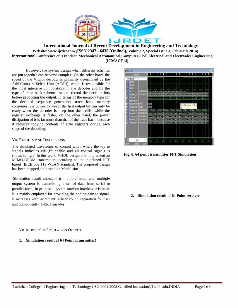
The simulated waveforms of control unit , where the top to
signals indicates clk ,fft enable and all control signals is
shown in fig.8. In this work, VHDL design and implement an
MIMO-OFDM transmitter according to the pipelined FFT
based IEEE 802.11a WLAN standard. The proposed design
has been mapped and tested on Model sim.
Simulation result shows that multiple input and multiple
output system is transmitting a set of data from serial to
parallel form. In proposed system random interleaver is built.
It is mainly employed for providing the coding gain to signal.
It increases with increment in user count, separation for user
and consequently BER Degrades.
VII. MODEL SIM SIMULATION OUTPUT
1. Simulation result of 64 Point Transmitter)
Fig. 8. 64 point transmitter FFT Simulation
2. Simulation result of 64 Point receiver
International Journal of Recent Development in Engineering and Technology
Website: www.ijrdet.com (ISSN 2347 - 6435 (Online)), Volume 2, Special Issue 3, February 2014)
International Conference on Trends in Mechanical,Aeronautical,Computer,Civil,Electrical and Electronics Engineering
(ICMACE14)
Tamizhan College of Engineering and Technology (ISO 9001:2008 Certified Institution),Tamilnadu,INDIA Page 164
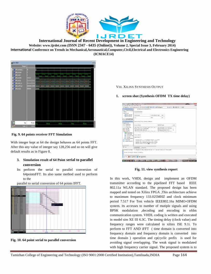
Fig. 9. 64 points receiver FFT Simulation
With integer kept at 64 the design behaves as 64 points FFT.
After this any value of integer say 128,256 and so on will give
default results as in Figure 8.
3. Simulation result of 64 Point serial to parallel
conversion
Its perform the serial to parallel conversion of
64pointsFFT. Its also same method used to perform
to the
parallel to serial conversion of 64 points IFFT.
Fig. 10. 64 point serial to parallel conversion
VIII. XILINX SYNTHESIS OUTPUT
1. screen shot (Synthesis OFDM TX time delay)
Fig. 11. view synthesis report
In this work, VHDL design and implement an OFDM
transmitter according to the pipelined FFT based IEEE
802.11a WLAN standard. The proposed design has been
mapped and tested on Xilinx FPGA ,This architecture achieve
to maximum frequency 133.025MHZ and clock minimum
period 7.517 For Test vehicle IEEE802.16a MIMO-OFDM
system. its accesses to number of mutiple signals and using
BPSK modulation ,decoding and encoding in ofdm
communication system. VHDL coding is written and executed
in model sim XE III 6.3C. The timing delay (clock value) and
frequency ranges were calculated in xilinx ISE 9.1i. To
perform to FFT AND iFFT ( time domain is converted into
frequency domain and frequency domain is converted into
time domain ) operation and cp(cyclic prefix is used for
avoiding signal overlapping. The weak signal is modulated
with high frequency carrier signal. The proposed system is to
International Journal of Recent Development in Engineering and Technology
Website: www.ijrdet.com (ISSN 2347 - 6435 (Online)), Volume 2, Special Issue 3, February 2014)
International Conference on Trends in Mechanical,Aeronautical,Computer,Civil,Electrical and Electronics Engineering
(ICMACE14)
Tamizhan College of Engineering and Technology (ISO 9001:2008 Certified Institution),Tamilnadu,INDIA Page 165
implement the mixed radix algorithm with random interleaver
concept. It increases the frequency level and clock signals
VI. CONCLUSION
This paper presents a new, very high speed FFT architecture
based on the Radix-2 algorithm. A fully pipelined, systolic
processing core of a 64-point FFT has been implemented in
both FPGA and standard cell technologies and validated in the
former case. The results demonstrate the very high operating
frequencies and the low latencies of both the FPGA and VLSI
implementations. The Same procedure was followed to
perform the receiver section and Calculated by frequency
and Time delay.
Future work in MIMO-OFDM is Application of CDMA in
MIMO OFDM.OFDMA Adaptive MIMO antenna selection
algorithms. Frequency hopping in the presence of frequency
selective channels.
Noise tolerance and interference cancellation.The modular
design of the Radix-2 allows them to be easily incorporated
into larger systems for computing large scale FFTs while a
fully registered, systolic architecture assures maximum
operating frequency. Future research by our group will focus
on the implementation of a reconfigurable FFT architecture,
capable of performing the FFT transform of 64, 4K, 256K or
16M complex points.
IX. REFERENCES
[1] H-G Ryu, “System design and analysis of MIMO SFBC CI-
OFDM system against the nonlinear distortion and narrowband
Interference,” IEEE Trans. Consumer Electron., vol. 54, no. 2,
pp. 368 –375, May 2008.
[2] Y. Houand and T. Hase, “New flexible OFDM structure for
consumer electronics communication systems,” IEEE Trans.
Consumer Electron., vol. 55, no. 1, pp. 191–198, Feb. 2009.
[3] H. Yu, M.-S. Kim, E. young Choi, T. Jeon, and S. Kyu Lee,
“Design and prototype development of MIMO-OFDM for next
generation wireless LAN,” IEEE Trans. Consumer Electron., vol.
51, no. 4, pp. 1134–1142, Nov. 2005.
[4] J. Soler-Garrido, D. Milford, M. Sandell, and H.
Vetter,“Implementation and evaluation of a high-performance
MIMO detector for wireless LAN systems,” IEEE Trans.
Consumer Electron., vol. 57, no. 4, pp. 1519 –1527, Nov. 2011.
[5] C.-S. Choi, Y. Shoji, and H. Ogawa, “Implementation of an
OFDM baseband with adaptive modulations to grouped
subcarriers for millimeter-wave wireless indoor networks,” IEEE
Trans. Consumer Electron., vol. 57, no. 4, pp. 1541–1549, Nov.
2011.
[6] S. H. Muller-Weinfurtner, “Coding approaches for multiple
antenna transmission in fast fading and OFDM,” IEEE Trans.
Signal Process., vol. 50, no. 10, pp. 2442–2450, Oct. 2002.
[7] Z. Iqbal and S. Nooshabadi, “Effects of channel coding and
interleaving in MIMO-OFDM systems,” IEEE Int. Midwest
Sym. on Cir. and Sys. (MWSCAS), Seoul, Korea, August
2011, pp. 1–4.
[8] J.-M. Lin, H.-Y. Yu, Y.-J. Wu, and H.-P. Ma, “A power efficient
baseband engine for multiuser mobile MIMO-OFDMA
communications,” IEEE Trans. Cir. and Sys. I: Regular Papers,
vol. 57, no. 7, pp. 1779 –1792, July 2010.
[9] Y.-N. Chang, “A low-cost dual-mode deinterleaver design,”
IEEE Trans. Consumer Electron., vol. 54, no. 2, pp. 326–332,
May 2008.
[10] Z. Iqbal, S. Nooshabadi, and H.-N. Lee, “Efficient interleaver
design for MIMO-OFDM based communication systems on
FPGA,” IEEE Int. Sym.on Consumer Electron. (ISCE),
Harrisburg, PA, June 2012, pp. 62–66.