design of power supplies for piezo legs and sic experiment1046325/fulltext01.pdf · degree project...
TRANSCRIPT

DEGREE PROJECT IN ELECTRONICS AND COMPUTER ENGINEERING, FIRST CYCLE, 15 HP STOCKHOLM, SWEDEN 2016
Design of power supplies for
Piezo LEGS and SiC experiment
KTH Student satellite MIST
SIMON JOHANSSON
KTH ROYAL INSTITUTE OF TECHNOLOGY SCHOOL OF INFORMATION AND COMMUNICATION TECHNOLOGY

Design of power supplies for
Piezo LEGS and SiC experiment
KTH Student satellite MIST
Simon Johansson 2016-06-12
Bachelor’s Thesis
Examiner
Carl-Mikael Zetterling
Academic adviser
Bengt Molin
KTH Royal Institute of Technology School of Information and Communication Technology (ICT) Department of Communication Systems SE-100
44 Stockholm, Sw eden

Abstract
KTH is funding a project whose goal is to send a satellite into space. This project is calledMIST (Miniature Student Satellite) which is assembled by a team of students at KTH. On thesatellite there are experiments that are invented by other teams, in two of those experiments apower supply is required. This thesis is a technical investigation on how to design the powersupply to both of those experiments, which are called SiC and Piezo LEGS. Piezo LEGS willinvestigate how their nanosized motors will behave and function in a space environment. SiCwill investigate how their silicone carbide transistors will be affected by the space environment.
A team made of four other students was selected to produce SiC experiments and a PCBin which this work is included. A literature study was done to get a better understanding ofhow power supplies work and to know how to select a good power supply. When the powersupplies were selected they were simulated to meet the requirements. The next step was to doa Printed Circuit Board(PCB) for the SiC experiment and Piezo LEGS to be able to test thepower supplies functionality in the physical world. Both of the converters reached the requiredoutput and characteristics working on their respective PCB. More time is needed for long timetesting and optimization on the PCB layouts.
Keywords– Silicon Carbide, Satellite, Electronics, Power Supply, Boost converter, Buck con-verter, Switching Converter, Linear Converter, PCB

Sammanfattning
MIST (Miniature Student Satellite) är ett av KTH subventionerat projekt vilket har som målatt skicka upp en satellit i rymden. Projektet kommer omfatta flera olika experiment. PiezoLEGS ska undersöka en motors funktionalitet i rymdmiljö. SiC ska undersöka hur Silicon carbidehalvledare och transistorer påverkas av rymdmiljön. Båda experimenten kräver varsin ström-försörjning för att fungera. Detta projekt ska undersöka kraven på strömförsörjning samt testaprototypen av ett kretskort för densamma.
Först genomfördes en förstudie av de två typer av regulatorer som vanligtvis används som ström-försörjning, den linjära regulatorn och switch-mode regulatorn för att förklara olika strömförsörjnings-teknologier, samt ta reda på de olika miljökraven. Baserat på förstudiens resultat erhölls kunskapför hur tester ska tas fram för funktionalitet av regulatorerna så att de når kraven för MISTför att sedan kunna producera de båda regulatorerna. Målet är att resultatet av simuleringarnapå strömförsörjningen ska stämma överens med utfallet av kretskorten som produceras. Mät-ningar genomfördes på prototyp kretskort som visade att simuleringarna var korrekta och gavströmförsörjningen rätt resultat på kretskorten. Några av funktionerna på regulatorerna hannej testas på grund av tidsbrist och mycket framtida arbete kvarstår.
Nyckelord– Kiselkarbid, Satellit, Elektronik, Strömförsörjning, Boost regulator, Buck regu-lator, Switch-mode regulator, Linjär regulator, PCB

Acknowledgments
The project period lasted between 28:th April to 17:th June and during that time, I have metmany interesting people, who have helped me with the bachelor thesis and the work with thepower supplies. First, I would like to thank the KTH for giving me the opportunity to workwith the MIST team satellite mission. It has been a great experience. Then I would like tothank my supervisor Bengt Molin and the examiner Carl-Mikael Zetterling for giving me theopportunity to work with the SiC team and to develop the experiment for the MIST satellite.Secondly, I would like to thank them for the help with ordering material and giving access toa workspace at KTH while doing the bachelor thesis, and for giving me feedback on the powersupply. Without their help, the work with the bachelor thesis would not have gone as effortlessly.
Furthermore, I would like to thank the SiC project team which consists of Hannes Paulsson,Mikael André, Johan Silverudd and Matthias Ericson for a fun time during this bachelor thesisand for their help with soldering and gathering information. The team worked well and helpedeach other in a good way and SCRUM worked well as project method. I would also like to thankMark Smith for helping the team with milling our boards. Without the opportunity to makeour own circuit boards in a couple of hours with the milling machine at KTH Kista, the workwould not have been done as fast as it was. It made the testing phase a lot shorter as we coulddo the testing earlier.
The company Linear Technology has helped me by consulting on how to choose the correctpower supply for the experiments. From them, I received test circuits as well as books to helpout with the understanding on how the converters work, as well as finding a suitable converterto fit the experiment and its requirements.
Contents
1 Introduction 11.1 Background . . . . . . . . . . . . . . . . . . . . . . . . . . . . . . . . . . . . . . . 11.2 Problem definition & Purpose . . . . . . . . . . . . . . . . . . . . . . . . . . . . . 21.3 Goal . . . . . . . . . . . . . . . . . . . . . . . . . . . . . . . . . . . . . . . . . . . 21.4 Benefits, Ethics and Sustainability . . . . . . . . . . . . . . . . . . . . . . . . . . 21.5 Delimitations . . . . . . . . . . . . . . . . . . . . . . . . . . . . . . . . . . . . . . 31.6 Methodology / Methods / Research Methodology . . . . . . . . . . . . . . . . . . 31.7 Outline . . . . . . . . . . . . . . . . . . . . . . . . . . . . . . . . . . . . . . . . . 3
2 Methodology 52.1 Literature study . . . . . . . . . . . . . . . . . . . . . . . . . . . . . . . . . . . . 52.2 Hardware selection . . . . . . . . . . . . . . . . . . . . . . . . . . . . . . . . . . . 52.3 Testing . . . . . . . . . . . . . . . . . . . . . . . . . . . . . . . . . . . . . . . . . . 5
3 Theoretical Background 63.1 How does a DC-DC Boost converter work? . . . . . . . . . . . . . . . . . . . . . . 63.2 How does a DC-DC Linear converter work? . . . . . . . . . . . . . . . . . . . . . 9
4 Choosing a power supply for space application 114.1 Requirements & Demands . . . . . . . . . . . . . . . . . . . . . . . . . . . . . . . 11
4.1.1 MIST . . . . . . . . . . . . . . . . . . . . . . . . . . . . . . . . . . . . . . 114.1.2 SiC & Piezo . . . . . . . . . . . . . . . . . . . . . . . . . . . . . . . . . . . 124.1.3 Physical . . . . . . . . . . . . . . . . . . . . . . . . . . . . . . . . . . . . . 13
4.2 Choosing the SiC in Space DC-DC linear converter . . . . . . . . . . . . . . . . . 144.3 Choosing the Piezo LEGS DC-DC Boost converter . . . . . . . . . . . . . . . . . 14
5 How the chosen converters works 165.1 Linear converter LT3062 . . . . . . . . . . . . . . . . . . . . . . . . . . . . . . . . 165.2 Switching converter LT8570 . . . . . . . . . . . . . . . . . . . . . . . . . . . . . . 16
6 EMC 19
7 Tests to meet the requirements 23
8 Implementation 258.1 Simulations . . . . . . . . . . . . . . . . . . . . . . . . . . . . . . . . . . . . . . . 25
8.1.1 Linear Converter . . . . . . . . . . . . . . . . . . . . . . . . . . . . . . . . 258.1.2 Switched Converter . . . . . . . . . . . . . . . . . . . . . . . . . . . . . . . 26
8.2 Printed Circuit Board(PCB) . . . . . . . . . . . . . . . . . . . . . . . . . . . . . . 288.2.1 Material & Program used . . . . . . . . . . . . . . . . . . . . . . . . . . . 288.2.2 Linear Converter . . . . . . . . . . . . . . . . . . . . . . . . . . . . . . . . 298.2.3 Switched Converter . . . . . . . . . . . . . . . . . . . . . . . . . . . . . . . 30
8.3 Purchase of components . . . . . . . . . . . . . . . . . . . . . . . . . . . . . . . . 328.4 Testing . . . . . . . . . . . . . . . . . . . . . . . . . . . . . . . . . . . . . . . . . . 34
9 Results 359.1 SiC results . . . . . . . . . . . . . . . . . . . . . . . . . . . . . . . . . . . . . . . . 359.2 Piezo LEGS results . . . . . . . . . . . . . . . . . . . . . . . . . . . . . . . . . . . 37
10 Discussion 40

11 Future work 41
12 Conclusions 42
References 43
A Appendix : Component calculations 45
List of Figures
1 CubeSat satellite and the different experiments. The picture is taken from theMIST Team dropbox by Kavithasan Patkunam . . . . . . . . . . . . . . . . . . . . 1
2 Classification of the different power supply technologies[10] . . . . . . . . . . . . . 63 Boost converter when switch is open. The inductor is charged with energy by the
input voltage and the output capacitor is discharging which leads to output ripple. 74 Boost converter when switch is closed. The output voltage is boosted by the mag-
netic field from the inductor. . . . . . . . . . . . . . . . . . . . . . . . . . . . . . . 75 How the linear works in the general case. The operational amplifier together with
Vref is the sensor unit which drives voltage to the transistor to adjust the outputvoltage. . . . . . . . . . . . . . . . . . . . . . . . . . . . . . . . . . . . . . . . . . 9
6 System schematic of the SiC experimental board . . . . . . . . . . . . . . . . . . . 117 Pattern of the linear converter LT3062. Image from Linear Technology Corpora-
tion datasheet for LT3062[16] . . . . . . . . . . . . . . . . . . . . . . . . . . . . . 168 Pattern of the switching converter LT8570. Image from Linear Technology Cor-
poration datasheet for LT8570[17]. . . . . . . . . . . . . . . . . . . . . . . . . . . 179 Block diagram of LT8570 which shows what is inside the integrated circuit and
the external components. Image from Linear Technology Corporation datasheetfor LT8570[17] . . . . . . . . . . . . . . . . . . . . . . . . . . . . . . . . . . . . . 17
10 The Sepic configuration of LT8570. Image from Linear Technology Corporationdatasheet for LT8570[17] . . . . . . . . . . . . . . . . . . . . . . . . . . . . . . . . 18
11 Different EMI producing loops. The green is the most dangerous and creates mostEMI. Image from Linear Technology Corporation from[15] . . . . . . . . . . . . . 19
12 An example of a long hot loop on a PCB which will emit more EMI. . . . . . . . 2013 An example of a short hot loop on the PCB which will emit less EMI. . . . . . . . 2014 The magnetic field is produced and what direction the magnetic field is canceled.
Image from Linear Technology Corporation[15] . . . . . . . . . . . . . . . . . . . 2115 How the shielding works. Image from Linear Technology Corporation from[15] . . 2116 How to solve the EMI problem in a better way using a cancellation layer. Image
from Linear Technology Corporation from[15] . . . . . . . . . . . . . . . . . . . . 2217 Linear regulator with the correct values for 10 V output. . . . . . . . . . . . . . . 2518 Linear regulator simulation results. . . . . . . . . . . . . . . . . . . . . . . . . . . 2619 The ciruit that was used to simulate the LT8570 . . . . . . . . . . . . . . . . . . 2720 The simulated result of the calculated values in the simulation . . . . . . . . . . . 2821 Output voltage and from this the ripple was calculated by taking the difference
between the highest and lowest value. . . . . . . . . . . . . . . . . . . . . . . . . . 2822 Schematic in Diptrace of the LT3062 converter that later is used to produce the
PCB . . . . . . . . . . . . . . . . . . . . . . . . . . . . . . . . . . . . . . . . . . . 2923 The final version of LT3062 PCB before it were milled. . . . . . . . . . . . . . . . 3024 Schematics in Diptrace of LT8570 which was used to produce the PCB. . . . . . . 3125 The final version of the PCB layout . . . . . . . . . . . . . . . . . . . . . . . . . 3226 Milled prototyp PCB that were used to test the converters functionality . . . . . . 3427 The transient response of LT3062. . . . . . . . . . . . . . . . . . . . . . . . . . . 3628 Final prototype PCB of the whole SiC experiment. LT8570 is not applied on this
version of PCB. . . . . . . . . . . . . . . . . . . . . . . . . . . . . . . . . . . . . . 3629 Power consumption of the SiC experiment circuit without the SiC transistor. . . . 3730 The transient response of LT8570. . . . . . . . . . . . . . . . . . . . . . . . . . . 3831 Output ripple with long EMC hot loop . . . . . . . . . . . . . . . . . . . . . . . . 3832 Output ripple with short EMC hot loop . . . . . . . . . . . . . . . . . . . . . . . . 39

List of Tables
1 Measurements that need to be done on the linear converter to show that the con-verter works. . . . . . . . . . . . . . . . . . . . . . . . . . . . . . . . . . . . . . . 23
2 Measurements that need to be done on the switching converter to show that theconverter works. . . . . . . . . . . . . . . . . . . . . . . . . . . . . . . . . . . . . 24
3 Capacitors purchased for the two converters . . . . . . . . . . . . . . . . . . . . . 334 Resistors purchased for the two converters . . . . . . . . . . . . . . . . . . . . . . 335 Inductor purchased for the switch-mode regulator . . . . . . . . . . . . . . . . . . 336 Diode purchased for the switch converter . . . . . . . . . . . . . . . . . . . . . . . 337 Converters purchased for SiC and Piezo . . . . . . . . . . . . . . . . . . . . . . . 348 Final result of the performance of the linear converter LT3062. . . . . . . . . . . 359 CNBS=Can Not Be Simulated. X meaning that the test was not done. . . . . . . 3510 Measured power consumption of LT3062 . . . . . . . . . . . . . . . . . . . . . . . 3711 The final result of the performance of the switching converter LT8570. X meaning
that the test was not completed. . . . . . . . . . . . . . . . . . . . . . . . . . . . . 3712 CNBS=Can Not Be Simulated. X meaning that the test was not done. . . . . . . 37

List of acronyms and abbreviations
Boost converter–A DC-DC converter that makes the voltage increase, for example 5 volt to 15volt.Buck converter–A DC-DC converter that makes the voltage decrease, for example 15 volt to 5volt.CCM – Continuous Conducting Mode. When a boost converter operates in continuous mode,the current through the inductor (IL) never falls to zero.CNBS – Can Not Be Simulated.DC-DC – Direct Current To Direct Current.DC-DC regulator – Another name for DC-DC converter.EMI – Electromagnetic radiation.ESR – Equivalent series resistance. A resistance that is present in inductor and capacitors whichis based on the inertia of the material used in the component.FBX – Feedback resistor pin in the LT8570 converter.MIST – The MIniature STudent satellite.OBC – On Board Computer. The computer which the MIST satellite will use as the main framecomputer which will send the data from the experiments back to Earth.OpAmp – Operational amplifier.PWM – Pulse-Width Modulation.PCB – Printed Circuit Board. A circuit board on which electrical components are soldered toget the desired functionality of the theoretical .Transient Response – How fast the circuit responses to changes in the system, for example howfast a linear regulator reacts to output changes and how fast these changes occur.Sepic – A mode that a boost converter can operate in.SiC – Silicon Carbide, a material used for making electronics which can withstand a more harshenvironment.Step down converter – Another name the Buck converter.Step up converter – Another name for the Boost converter.Switched-mode power supply – Another name for a switching converter.VFB – Feedback voltage: A voltage taken from the output in to OpAmp.Vref – A voltage reference value that goes in to an OpAmp, used in regulators to get feedbackof what the output is to stabilize changes occurred at the output. Usually low, around 1.2 V.X7R– Temperature rating on the capacitor.
1 INTRODUCTION Simon Johansson
1 Introduction
This project is a study of choosing the optimal power supply for a CubeSat satellite. Therequirements on the electronics are substantial in space which requires a more in-depth researchinto which DC-DC converter is needed for the power supply. I will investigate the Buck converteras well as the Boost converter for a student satellite called MIST for the Royal Institute ofTechnology (KTH).
1.1 Background
The idea of this project originates from MIST(The Miniature Student Satellite) which is asatellite project at KTH[1]. MIST is a 3U CubeSat satellite that is being built by student teamsat KTH to transport experimental projects out in space to measure how space influences theirexperiments and send these data back to Earth. The different teams work on selective aspectsof the CubeSat satellite. For example, one team investigated and calculated the orbit which thesatellite is travelling around the Earth. The satellite is scheduled to launch at the earliest 2017.
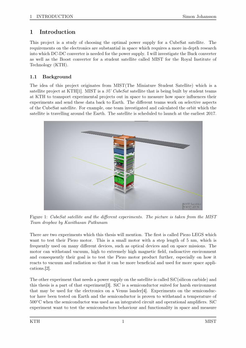
Figure 1: CubeSat satellite and the different experiments. The picture is taken from the MISTTeam dropbox by Kavithasan Patkunam
There are two experiments which this thesis will mention. The first is called Piezo LEGS whichwant to test their Piezo motor. This is a small motor with a step length of 5 nm, which isfrequently used on many different devices, such as optical devices and on space missions. Themotor can withstand vacuum, high to extremely high magnetic field, radioactive environmentand consequently their goal is to test the Piezo motor product further, especially on how itreacts to vacuum and radiation so that it can be more beneficial and used for more space appli-cations.[2].
The other experiment that needs a power supply on the satellite is called SiC(silicon carbide) andthis thesis is a part of that experiment[3]. SiC is a semiconductor suited for harsh environmentthat may be used for the electronics on a Venus lander[4]. Experiments on the semiconduc-tor have been tested on Earth and the semiconductor is proven to withstand a temperature of500C when the semiconductor was used as an integrated circuit and operational amplifiers. SiCexperiment want to test the semiconductors behaviour and functionality in space and measure
KTH 1 MIST
1 INTRODUCTION Simon Johansson
how the transistors will react to that environment so it can be used in future space missions.This thesis will be addressing how a DC-DC converter is working and how to design one forthe SiC experiment and the Piezo motor. Two other theses will deal with the design of theSiC experimental test circuit. The first thesis will deal with the measurement of SiC transistorsin the experiment, and the second thesis will deal with the microcontroller that will make themeasurements and send the data to the satellites onboard computer(OBC).
1.2 Problem definition & Purpose
The experiments with SiC transistors and Piezo motor need correct voltage level to function.This needs to be investigated to meet the requirement from the environment and product. TheCubeSat satellite can supply 3.3 V, 5 V and 14 V from the battery. The two experiments re-quires other voltage levels. To solve this problem we need to design a power supply for each ofthe experiments.
As the satellite will be located in space, this will result in a higher demand on the powersupply than regular power supplies. An example of this is the use of electrolyte capacitors willbe destroyed in a vacuum. This thesis is to investigate how to choose power supplies to meet theharsh demands in space, to meet the requirements from both experiments and be safe enoughnot to short circuit the satellite.
1.3 Goal
The intention is to design two DC-DC converters that can endure a hostile environment andthat are secure enough that the converters do not short-circuit the satellite. They should alsomeet the demand to supply enough voltage to the Piezo motor and SiC transistors and as suchthe goals are:
• Supply the Piezo motor with 48 V and 15 mA
• Supply the SiC transistors with 10 V and 10 mA
1.4 Benefits, Ethics and Sustainability
The investigation of how the SiC will behave in space will benefit future space exploration.With the data acquired from the experiments, KTH will get more knowledge which will lead toa better implementation of electronics and power supplies on other space missions. An exampleis the Venus lander, another example is Piezo LEGS which will continue to improve their motorfor future space missions. It will also benefit the MIST team so they can test the onboardcomputer(OBC) together with the experiments. For example, evaluate their communicationprotocol.
There are environmental effects that the MIST project can produce for example, toxic ma-terials and space debris[5][6]. The materials on a satellite are more advanced which can lead toa choice of electronics which are more toxic to health and affect the people coming in contactwith them so this should be handled with care and be something for future research[7]. Spacedebris is a more pressing matter to regulate as there is an increase of debris that is in orbitaround Earth which leads to a higher possibility that equipment is being hit by the debris.Keeping this to a minimum is important so other spacecraft do not get hit. MIST has a demandand a plan to minimize the debris and the plan is to make the CubeSat satellite incinerate(inthe atmosphere) when the experiments are finished.
KTH 2 MIST
1 INTRODUCTION Simon Johansson
1.5 Delimitations
The delimitation of this work is that it is strictly to satisfy the requirements on the productsthat are being designed for the experiments. Meaning that this work is delimited to be about aboost converter(step-up) and linear (step-down)converter. Therefore an in-depth analysis of theDC-DC linear converter(Step Down) and DC-DC Boost converter is being investigated. Mean-ing that transformer regulators or Sepic configured regulators will not be researched.
As this is a collaboration with two other teams, information about the different parts of theexperiment can be found in their respective reports. First Hannes Paulsson and Mikael Andréinform about the hardware and software of the SiC experiment in "Hardware design and softwaredevelopment of microcontroller for SiC in space experiment on student satellite MIST"[8]. Theyinvestigate what kind of low power microcontroller that can be used for reading temperaturesensors and sending data to the on board computer. Secondly Johan Silverudd and MatthiasEricson are investigating and designs a plan how the transistors shall be measured in their report"Design of measurements circuits for SiC experiment"[9]. They investigate how to measure theSiC transistors and construct the electronic circuit to do this so the microcontroller can readthe temperature on the transistors.
1.6 Methodology / Methods / Research Methodology
The research methodology used is this report is first a qualitative literature study for findinginformation on how the DC-DC converters work as power supply and how the electronics areaffected by space. The next part of the thesis will be about comparing the different convertersand chose one that is capable to the problem specified with associated requirements. Then thestudy goes into designing the product for testing and to guarantee that the converters work asintended. This means that the report is a technical report so other students can read this andunderstand how the power supply on the SiC and Piezo were produced and what the performanceof power supply is.
1.7 Outline
The reports begin with an Introduction where the background of the thesis is explained. It willexplain which the clients are and what goal that the thesis should achieve. In Methodology thereare explanations on how the thesis is planned to investigate the problem of choosing the correctpower supply. Theoretical background deals with theoretical groundwork, that is how DC-DCconverters work in theory, and the different types of converters that exist.
Chapter Choosing a power supply for space application is about the requirements that the powersupply has to meet. In chapter How the chosen converters work there is an explanation how thechosen converters operate.
Chapter EMC is about the EMC requirements that will be set on the converters, primarilythe switching converter. The chapter Tests to meet the requirements is about the tests that willbe carried out to ensure that the power supply satisfies the requirements set from the experi-ments.
Chapter Implementation deals with the production of the power supply. It will mention thesimulation of the power supplies and the selection of components, PCB fabrication, and millingthe circuit boards. Then in chapter Results will show the result and performance of the powersupplies. In chapter Discussion the result is discussed as well as the elections of converters.
KTH 3 MIST

1 INTRODUCTION Simon Johansson
Chapter Future work goes through what future research should be focused on and in chapterConclusion the report is finishing off with conclusions about this project.
KTH 4 MIST
2 METHODOLOGY Simon Johansson
2 Methodology
2.1 Literature study
It is important to acquire experience and information on how power supply functions so it be-comes easier to select a power supply that is adapted to meet the requirements of this project.This requires that a literature study is to be performed. This information should be easy tounderstand and widely obtained, meaning that many different sources will be visited and wherethe best information will be selected to this thesis. For example, Wikipedia can be a beginningfor finding books and references, NASA and ESA(European Space Agency) will be used as theyare experts in producing electronic equipment for space missions. Scientific reports will be usedfor increasing the depth of knowledge in specific areas.
To find general information about the power supplies, books and research will be used be-cause that is where the best information is available and simultaneously explains it in an easyway. Other sources that will be used is the producers of power supplies which may be able tohave information about how the power supplies are functioning. This will be companies likeLinear Technology and Texas Instruments.
2.2 Hardware selection
The choice of hardware will be based on the requirement made on the product. It is, therefore,important to do research on the requirements of the power supply. Information will be found onvarious space organization where one can find the requirements set by the environment on thehardware. Another source is the MIST group’s previous work which has investigated some ofthe environment requirements for their power supply. The producer of the CubeSat satellite hasimportant information on the battery used in their satellite in which the power supplies will beconnected to. There are also SiC and Piezo requirements that must be met, which is somethingthat must be investigated further. Then there are the physical requirements that are inherentin the power supplies such as transient response and quiescent current that will affect what kindof DC-DC converter to be chosen as a power supply. It is, therefore, important to communicatewith MIST, Piezo, and SiC to quickly develop a specification for the power supply.
2.3 Testing
In order to ensure that the requirements are achieved, it is important to develop a test plan.Since the objective is to design a product it is important to verify that it works as intended.The test plan will be statistically significant as it is important to verify that the product isfunctional. This is calculated using a mathematical statistics confidence interval. The testingwill take place at KTH in Kista Laboratory environment where a prototype circuit board isbeing produced and soldered for testing.
KTH 5 MIST

3 THEORETICAL BACKGROUND Simon Johansson
3 Theoretical Background
Different power supplies are used in many applications. A couple of examples is the AC-DCconverter from the electrical outlets in the house that converts the AC voltage from the powergrid to a DC voltage. Another example is the DC-DC converter on small electronic devices suchas microcontrollers and medical equipment which can use DC-DC converters to set voltage levelsto their peripherals. There are numerous power supplies that can be utilized and each has theirdifferent niches. As can be seen in the picture below there are two different classifications usedas power supply. First is the linear converter and secondly is the switching converter[10].
Figure 2: Classification of the different power supply technologies[10]
Both of the classification have their uses and the following section below will focus on explainingthe linear series regulator and switching PWM regulator as they are the ones that will be used.
3.1 How does a DC-DC Boost converter work?
The DC-DC Boost converter uses an inductor and capacitor to boost the output to highervoltage compared to the input voltage with the use of a transistor switch[10][11][12][13]. Thetransistor is switched on and off with a PWM(Pulse-width modulation) signal. When the switchis ON the inductor is storing energy in a magnetic field made from the input power source thatgoes through the inductor and when the switch is OFF the charged up inductor is releasing itsenergy to the output capacitor and load. The voltage from the inductor is added with the inputvoltage increases the output voltage. This behaviour can be seen in Figure 3 and Figure 4.
KTH 6 MIST
3 THEORETICAL BACKGROUND Simon Johansson
Figure 3: Boost converter when switch is open. The inductor is charged with energy by the inputvoltage and the output capacitor is discharging which leads to output ripple.
Figure 4: Boost converter when switch is closed. The output voltage is boosted by the magneticfield from the inductor.
Figure 3 explains the current path in a Boost converter when the PWM signal is high(ON)which will supply the gate voltage on the transistor and turn it on. There is virtually no currentflowing in the remainder of the circuit as the combination of the diode, output capacitor, and theload represents a much higher impedance than the path directly through the heavily conductingtransistor. During this phase, the inductor stores energy in its magnetic field. The next phaseis explained in Figure 4. When the PWM signal is low the transistor is switched off and theinductor creates a counter-electromotive force which generates a voltage that is added in serieswith the input which flows through the diode. This higher voltage is now (VIN +VL) as there isno current path through the transistor which leads to forward biases diode which is resulting inthat the current runs through the diode which charges up the capacitor to VIN +VL ,minus the
KTH 7 MIST

3 THEORETICAL BACKGROUND Simon Johansson
small forward voltage drop across the diode, and supplies the load. The capacitor is dischargedin Figure 3 which leads to a small output ripple as there is a little time when the switch is off. Asthe switching frequency of the PWM is high(in kHz or MHz) the output will be almost constant.
The number of electrical components needed for a working boost converter is the inductor,diode, conductor, transistor and the PWM circuit. Energy stored in the inductor is affectedwhen the diode and switch are open or not. The diode is now reversed biased and the voltageacross it is approximately equal to -V0. If the switch is closed and diode is open the inductorhas the voltage across it:
vL = Vin = LdiLdt
(1)
and the maximal current in the inductor is therefore
iL =1
L
∫ top
0Vin dt⇒
VinDT
L+ iL(0) (2)
where D is the ON duty ratio and is defined as
D =tonT, T =
1
f.
where ton is the amount of time the PWM-signal is on(1) and iL(0) is the inductor current initialvalue. This leads to that the inductor current is increasing with the rate of
diLdt
=VinL. (3)
When the switch is turned off and the diode switch is turned on the inductor will discharge thestored magnetic field at the rate of
VL = VIn − VOut = LdiLdt
< 0 (4)
and the current with the rate ofdiLdt
=Vin − Vout
L> 0 (5)
The diode is now letting the current through and is charging up the capacitor(C) and driving theload(RLoad). The theoretical DC output voltage is determined by the input voltage (Vin) dividedby 1 subtracted by the duty cycle (D) of the PWM signal, which will be some figure between 0and 1 (corresponding to 0 to 100%) and therefore can be determined using the following formula:
Vout =Vin
1−D(6)
The boost converter has poor ability to prevent hazardous transients and failures. If positivevoltage surges appear at the input and exceed the output the diode will be destroyed by acurrent spike, that may be introduced by outside sources like the sun or from other experiments.It is also a possibility that this may happen when the boost converter starts up. This can besolved with a diode between Vin and the output capacitor. Power supplies applications wherethe switching regulators are preferable is therefore
1. Can reach higher level of voltage outputs
2. Is able to step up and step down voltage
3. Has better efficiency
4. Creates less heat due to better efficiency
KTH 8 MIST
3 THEORETICAL BACKGROUND Simon Johansson
3.2 How does a DC-DC Linear converter work?
The DC-DC linear converter is used when you want the output voltage to be lower than theinput voltage. The linear converter is regulating the output voltage with a sensor circuit andadjusts voltage drop to keep output voltage constant[10][14][12]. The basic sensor circuit can besimulated as an amplifier that regulates the transistor using the output and a reference voltage.For example, if Vref is 5 V then the output will be 5V. But that isn’t the best way to utilizethe sensor circuit because it can be problematic to get that high of Vref . Instead you connect aload circuit on one the negative input of the OpAmp(Operational amplifier) to control the levelof the output. This will control the gate on the transistor and regulate the amount of voltageflowing on the output. This can be seen in Figure 5.
Figure 5: How the linear works in the general case. The operational amplifier together with Vrefis the sensor unit which drives voltage to the transistor to adjust the output voltage.
To utilize the OpAmp to amplify the voltage to the transistor you add resistors to amplify thevoltage according to:
Av =VOutVref
=Ra +RbRa
⇔ VOut = VrefRa +RbRa
(7)
For example if Vref is 2 and Ra and Ra 50 ohm we get 4 V as the output voltage. As can benoted it is an easy circuit to build with basic components which is one of the major reasons touse the linear converter. The other major reason to use a linear regulator is its stability dueto no switching components inherit in its design. But the linear regulator has drawbacks. Theregulator has substantial problems with power efficiencies as all the current needs to go throughthe transistor the power dissipation is (VIn-VOut)*IOut. Then the efficiency is the defined by
POutputPOutput + PLoss
=VOut ∗ IOut
VOut ∗ IOut + (VIn − VOut) ∗ IOut=VOutVIn
. (8)
As we can note the larger the values between the input and output voltage so does the efficiencygets lower and get turned into heat. The other way around is true as well as the values are closerand closer the efficiency gets better. But be cautious that the voltage level on the input is notthe same as on the output which will lead to that the transistor leaves its linear mode(whichit need to work properly) and the linear regulator will stop working. Applications, where thelinear regulators are preferable as a power supply, is therefore
1. Simple/low cost as the number of components are low
KTH 9 MIST

3 THEORETICAL BACKGROUND Simon Johansson
2. Low noise/low ripple as there are no components in the linear regulator that is disturbingthe output voltage
3. Fast transients
KTH 10 MIST

4 CHOOSING A POWER SUPPLY FOR SPACE APPLICATION Simon Johansson
4 Choosing a power supply for space application
This chapter will investigate what the requirements are on the power supply. First an investi-gation of the requirements from MIST then SiC and Piezo LEGS. From these requirements, thechoice of power supplies will be defined. The system layout of the SiC experimental board canbe seen in the figure below
Figure 6: System schematic of the SiC experimental board
4.1 Requirements & Demands
There are numerous requirements that will affect how to choose the correct power supply. First,there are the demands from the MIST team about the electronics on the satellite. It shouldnot affect other experiments or other parts of the satellite. The second requirement is from thetwo experiments that need the converters for their different experiments. And the last is howthe physical environment interacts with the electronic and how that may affect how the powersupply behaves.
4.1.1 MIST
The MIST team has these requirements:
• Battery voltage is between 12 and 16 V
• Keep the current as low as possible
• A fuse so the power supply is unable to short-circuit the satellite’s battery
• As low magnetic field as possible so it will not affect other experiments
• 90 x 94 mm circuit board dimensions
• Be able to shut down the experiment
KTH 11 MIST
4 CHOOSING A POWER SUPPLY FOR SPACE APPLICATION Simon Johansson
• Low power consumption
The battery used on the satellite is a NanoPower P-series P31us which supplies both of theconverters with 12-16 V and current directly through Vbat. Therefore MIST is firm on that bothof the converters needs a circuit breaker, based on the current level, to be able to switch onand off the power supplies so the satellite is not short-circuited as the converters are directlyconnected to the battery pack.
The satellite has a confined space available which translates to the small distance between exper-iments which leads to that electromagnetic radiation(EMI) from each experiment can affect eachother. Thus it is important to keep radiation as low as possible. In the DC-DC converter, theparts that may produce EMI is the inductor and the switching event in the switching converterand heat from the linear converter. It is important that these part, as well as EMC, is taken intoconsideration when choosing the converter. A good rule of thumb is to follow AN-139[15],whichwill be used during this thesis.
The choice of the satellite is CubeSat which has fixed dimensions for how big the experimentscan be. The dimensions of the PCB is 90 x 94 mm. Meaning that the converters need to be assmall as possible to make sure that all the components fit on the circuit board, by having fewexternal components.
4.1.2 SiC & Piezo
There are two experiments that are in need of a power supply and both of them has a differentrequirement that needs to be met. SiC needs a regulator that lower the voltage from the batterydown to 10 V and Piezo LEGS needs a higher voltage, from battery level to 48 V to run theirmotor. Understanding the requirement is fundamental for making sure that the power supply isworking properly and does not affect the other experiments on the satellite.
The requirement from SiC is:
1. 10 V output
2. 10 mA output
3. Keep its voltage even when the temperature is rising and when the converter is affectedby radiation
4. Stable output and fast reactions to variations on the input and output
5. Be able to turn on and off the regulator using a microcontroller
The 10 V and 10 mA outputs are for supplying enough power to the electrical circuitry so theexperiment gets started. The 10 V power line will be used for the transistors to start so theycan be measured so the data can be sent back to earth. The low difference between the batteryand regulator makes this a good candidate to use a linear step-down converter.
It is important to take security measures so that no other equipment get affected by the con-verters. For example, if the converter stops working the experiment will stop working. EMI willaffect the electronics, therefore, it is important that the converter will not change its behaviourfrom these stresses.
KTH 12 MIST
4 CHOOSING A POWER SUPPLY FOR SPACE APPLICATION Simon Johansson
Making sure that the output is stable and not acquiring big variation is vital for this appli-cation so that there are no big changes in the circuitry around the transistors. This may affectthe stability of the whole circuitry. Without this stability, the power supply can become unstableand damage the circuitry of the experiment or worse the satellite.
The experiments have specific times when they need to be active. This will be controlled by theOBC by shutting down the power supply. This is implemented so MIST can control if any of theexperiments needs to be shut down due to malfunction or to save power on the battery. This isone of the major criteria that needs to be fulfilled. Piezo LEGS motor have similar demands:
1. 48 V output
2. 15 mA output
3. Security measure in the form of a fuse on the input
4. Be able to turn on and off the regulator using a microcontroller
5. Output ripple should not be higher than ± 0.3 V
The 48 V and 15 mA is needed to power the motor. There is a need to make sure that the powersupply does not affect the motor with current/voltage spikes so that the motor gets destroyedand as with SiC you should be able to shut down the regulator. The ripple should be as lowas possible so the current is as close to a DC current otherwise the ripple effect can produceinstability in the circuit.
4.1.3 Physical
In space the satellite is in an environment that affects the electronics with vacuum, radiation,temperature variations and vibration. This in turn affects what electrical components and ma-terial that can be used and how to heat dissipation will be on the converters that are beingused. There are also internal physical demands such as the noise levels, transient response andelectromagnetic pulses that need to be met to make sure that the power supplies is stable andfunctional in the correct voltage level.
In space there is cosmic radiation from the sun. The sun affects electronics on earth withsolar flares. But this depends on what the orbit of the satellite is. MIST investigated this andthe result was that the orbit of the satellite is so low that the radiation level is low enough thatthe electrical components do not need to be radiation classified. The vacuum in space will affecthow to chose the electrical components. Any components that are made of a fluid is forbidden. Acapacitor made from electrolytes is banned as they will be destroyed if frozen. Instead, ceramiccapacitors are recommended.
It is a rocket that is sending the CubeSat satellite into space. The amount of force the rocketproduce is inducing the vibration and that vibration can destroy the electrical components onthe PCB. This means that the choice of components is vital to make sure that the converterskeep their performance and that an extensive testing phase needs to be carried out.
The power supplies have internal systems that can effect how good the power supplies work.Firstly there is the transient response which is how fast the converter reacts to changes inthe output or input. Secondly the noise from the converter. The PWM-switching movementintroduces a noise into the system that needs to be stable.
KTH 13 MIST
4 CHOOSING A POWER SUPPLY FOR SPACE APPLICATION Simon Johansson
4.2 Choosing the SiC in Space DC-DC linear converter
Based on the requirement a linear regulator is best suited as the power supply for SiC as the stepdown is low, easier to build, is more stable and has the same shutdown feature as the switchingconverter. Searching for the converters is done at Texas Instruments and Linear Technology asthey are one of the biggest manufacturers of integrated circuits and they have their main officeat Kista. Using LTspice the circuits were simulated to make sure that the output is correct andthat the circuit is stable and is working as intended.
The linear converter is more efficient as the step-down levels are lower which makes it bet-ter suited for this application. The maximum input from the battery on the satellite is 16 Vand therefore the worst case efficiency is
VoutVin
=10
16= 0.625 = 62.5%. (9)
The switching converter is having a better efficiency but as the implementation of the experi-ment is in space repairs are not doable if something is failing. Keeping the noise on the circuitis a higher priority so a linear converter is a better choice. So the linear converter is a muchbetter approach as long as the heat dissipation is acceptable.
The circuit board that is being used on CubeSat is small so it is important that the convertersare small. Also, the SiC experiments need space for their test circuits. As the linear converterneeds very few external components this will result in a smaller space used on the circuit boardcompared with the switching converter that needs more external components for making thecircuit stable and working as intended.
Based on the requirement, searches for the right power supplies began at the biggest electroniccompanies, Texas Instrument and Linear Technology. The motivation behind this was that theyare one of the biggest producers of electrical circuits and that they are within walking distancefrom KTH Kista and such can be consulting with them about their products. With the knowninputs and outputs. These were put in the search box were we found around 10 linear regulatorsat each website that could be used, but checking against the other requirements only 2-3 metthose. In the end, the requirement that had the highest priority was how big the power supplywas as the goal is to have a small converter as possible. The converter that in the end wasselected was the LT3062 from Linear Technology as it was small and had very low quiescentcurrent. The next step was to check the circuit with calculated values on the electrical compo-nents from the datasheet and with those values simulate how the converter behaves. More exactinstructions on the simulation can be found under Implementation under Simulation
4.3 Choosing the Piezo LEGS DC-DC Boost converter
Choosing the correct boost converter depends on variables such as voltage input, voltage/currentoutputs, stability of the circuit, characteristics of the converter and efficiency of the converter.Making sure to meet the requirement of all these variables is critical for choosing the correctconverter. As the linear converter mostly is used as a Buck converter the Boost converter needsto be a switching converter.
Both SiC and MIST demands that the converter needs to be able to shutdown so the bat-tery will not get discharged or to save power. The shutdown feature is needed to shut down theexperiment if needed to, for example in the case if one of the experiments is failing. Then theOBC(On Board Computer) must be able to shut down the experiment if this occurs. Another
KTH 14 MIST

4 CHOOSING A POWER SUPPLY FOR SPACE APPLICATION Simon Johansson
feature is to be able to have both Boost and Sepic configuration so both of the configuration ofthe converter can be tested to investigate what configuration that is best suited for the Piezomotor in regards to safety and stability. Sepic is a more safe configuration of a Boost converterbecause there is a capacitor between the inductor and diode. Sepic configuration is safer as thecapacitor stops the input voltage to reach the output when the converter is shut down.
The ratio of input versus output voltage is so high and that the Piezo experiment needs aBoost converter and it would be recommended to use a switching regulator. After consultingwith a field application engineer from Linear Technology the best-suited Boost converter wasthe LT8570. It was small enough to fit the board and was also recommended by the Piezo LEGSteam and had all the necessary characteristics for their requirement.
KTH 15 MIST
5 HOW THE CHOSEN CONVERTERS WORKS Simon Johansson
5 How the chosen converters works
To use the converter it is important to have an understanding of its functionality and keep trackof its layout to optimize the design of both of the converters. This is to get an understanding ofhow the external component of the circuit influences the functionality of the power supply andhow to calculate their values. The information about their function is used to make the PCBbetter and follow the data sheet guidelines on how to lower noize and EMI. The following sectionwill describe the two converters that was selected and how they operate. More information aboutthem can be found in the datasheets.
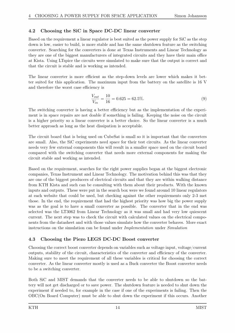
5.1 Linear converter LT3062
LT3062 is a linear regulator that takes in a higher voltage and reduces it to a lower voltage. Itdoes this by choosing the correct values of two resistors that are connected to the ADJ pin. Inthe image below we have the footprint of the integrated circuit.
Figure 7: Pattern of the linear converter LT3062. Image from Linear Technology Corporationdatasheet for LT3062[16]
The LT3062 integrated circuit consists of 8 pins, REF/BYP connected to pin 1, the ADJ pinconnected to pin 2, pin 3 and 4 is output, pin 5 and 6 inputs, SHDN pin 7, pin 8 ground.REF/BYP stands for Reference/Bypass. By attaching a capacitor on this pin will activate thesoft-start performance of the LT3062. The capacitor helps reduce the noise on the output. ADJ(Adjust) pin is the error amplifier’s inverting terminal which sets the output voltage. OUT(output) pins supplies the output with the desired voltage. To minimize oscillations, a capacitorplaced at the output needs to be at least 3.3 µF. IN (Input) pins provide power to the inputsof the integrated circuit. To lower input impedance a capacitor can be mounted at the inputof a value ranging between 1 µF to 10 µF. SHDN (shutdown) is responsible for turning off oron the LT3062. By grounding this pin you will turn off the converter. It is recommended toplace a resistor which acts as a pull-down resistor so stray current or voltages can not affect thepin. GND is the ground pin for LT3062. The calculations for the capacitors and resistors canbe read under Implementation.
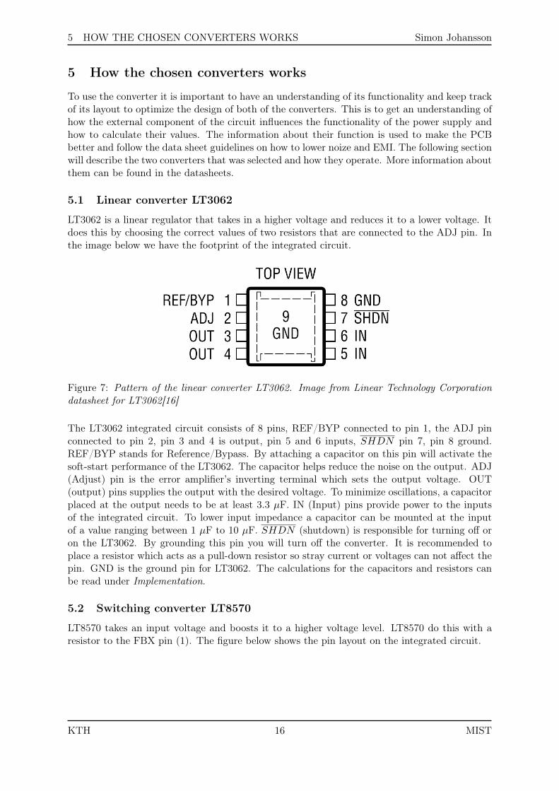
5.2 Switching converter LT8570
LT8570 takes an input voltage and boosts it to a higher voltage level. LT8570 do this with aresistor to the FBX pin (1). The figure below shows the pin layout on the integrated circuit.
KTH 16 MIST
5 HOW THE CHOSEN CONVERTERS WORKS Simon Johansson
Figure 8: Pattern of the switching converter LT8570. Image from Linear Technology Corporationdatasheet for LT8570[17].
To explain the function of the pin layout on the LT8570 and the external component effect onLT8570, it requires that we look at the block diagram.
Figure 9: Block diagram of LT8570 which shows what is inside the integrated circuit and theexternal components. Image from Linear Technology Corporation datasheet for LT8570[17]
In the block diagram, we see that the adjustable oscillator starts a switch(SR1) on the positiveedge. This allows the transistor Q1 to start and transport power to A4 from VIN . The voltagefrom A4 is then added to a stabilizing ramp which is connected to comparators A3 positiveinput. When the voltage level of the A3 negative input exceeds level on the positive input thelatch resets and turns off Q1 again. In this manner, the switching time is determined. How longon and off time of the switching will take is determined by the FBX resistor and VC circuit.The difference between FBX and the reference(1.2V) voltage level sets the correct power levelto the output. Meaning that the error amplifier sets the correct peak current level to keep theoutput in regulation
KTH 17 MIST

5 HOW THE CHOSEN CONVERTERS WORKS Simon Johansson
VC at pin 2 consists of a network of two capacitors, parallel to each other, and a resistor.It’s main task is to influence transient response and keep the circuit stable. Pin 3 consisting ofvoltage in (Vin), and if it falls below 2.35V the converter switches off. The converter will notturn on again until the voltage is high again. Pin 4 is the collector of NPN transistor whichtransports the current to A4 and is on or off depending on the SR1 latch. For the LT8570 to bein the ON state is necessary to understand the pin 3, 5 and 7. First, SHDN must be over 1.3V.This turns the latch SR2 on due to the OR-gate which charges the capacitor on pin 7. Thismakes the LT8570 to have a soft start before it begins running. Pin 8 is used to synchronize thecontroller with an external clock. The high voltage level of the clock needs to exceed 1.3V, andthe low level should be less 0.4V. If lower than this the internal clock will turn on instead. Pin7 sets the frequency to a fixed level. Which frequency used depends on the desired application.
LT8570 has a mode called Sepic which can be seen below.
Figure 10: The Sepic configuration of LT8570. Image from Linear Technology Corporationdatasheet for LT8570[17]
Now there is a capacitor after the inductor L1 that protects the output if the regulator is shortedor is destroyed by not letting any current to the output. It also helps to keep voltage spikes tobe less dangerous on the output. More information can be found in the data sheet of LT8570.
KTH 18 MIST

6 EMC Simon Johansson
6 EMC
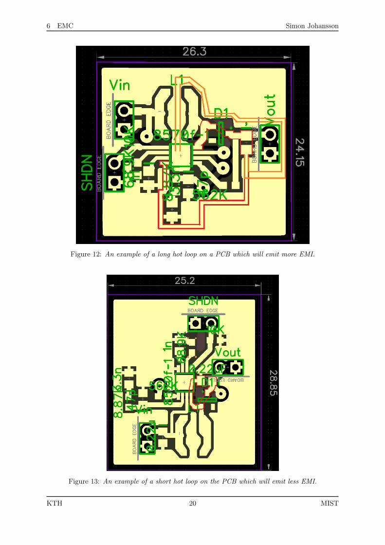
The LT8570 is a switching converter which is prone to emit electromagnetic interference(EMI)because of the PWM-switching. To make a power supply stable and to make it work with lowdisturbances the printed circuit board(PCB) layout is important[15]. This section will explainwhat to scrutinize when designing a switching converter to keep the EMI radiation as low aspossible. The layout must keep the important loops that the converter has as short as possible.There are different kinds of loops for LT8570. One small loop from Cin through the inductorand through the integrated circuit if the diode acts as a switch and not let anything through.Another is a loop from Cin through the diode while the integrated circuit is open and Cout toground and back to Cin. The last one, the hot loop, is the one that is emitting the most EMIand it emerges when both the diode and the integrated circuit is on. Then the high switchingfrequency path is going through the diode and Cout down to ground back into the integratedcircuit. The loops can be seen in the picture below
Figure 11: Different EMI producing loops. The green is the most dangerous and creates mostEMI. Image from Linear Technology Corporation from[15]
Minimizing this hot loop is the main priority. Otherwise LT8570 can become unstable and notreach the required output. To counteract the hot loop a good PCB layout is important. For theLT8570 the hot loop is the most important to keep as small as possible. The difference can beseen on the two PCB that was created for this thesis.
KTH 19 MIST
6 EMC Simon Johansson
Figure 12: An example of a long hot loop on a PCB which will emit more EMI.
Figure 13: An example of a short hot loop on the PCB which will emit less EMI.
KTH 20 MIST
6 EMC Simon Johansson
The result of how the EMI affects the performance of LT8570 in the above picture and can beread under 9 Results under 9.2 Piezo LEGS results.
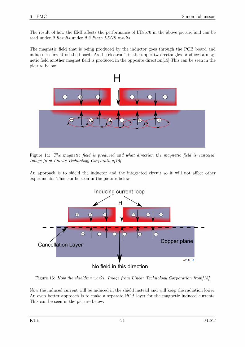
The magnetic field that is being produced by the inductor goes through the PCB board andinduces a current on the board. As the electron’s in the upper two rectangles produces a mag-netic field another magnet field is produced in the opposite direction[15].This can be seen in thepicture below.
Figure 14: The magnetic field is produced and what direction the magnetic field is canceled.Image from Linear Technology Corporation[15]
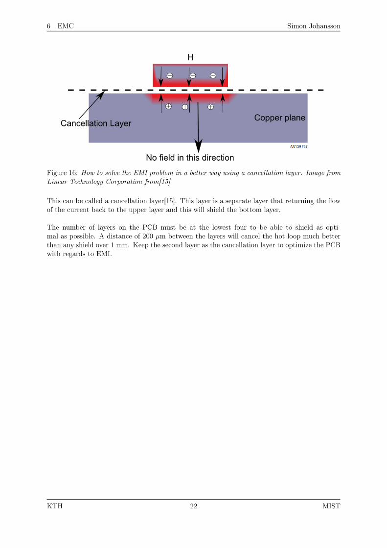
An approach is to shield the inductor and the integrated circuit so it will not affect otherexperiments. This can be seen in the picture below
Figure 15: How the shielding works. Image from Linear Technology Corporation from[15]
Now the induced current will be induced in the shield instead and will keep the radiation lower.An even better approach is to make a separate PCB layer for the magnetic induced currents.This can be seen in the picture below.
KTH 21 MIST
6 EMC Simon Johansson
Figure 16: How to solve the EMI problem in a better way using a cancellation layer. Image fromLinear Technology Corporation from[15]
This can be called a cancellation layer[15]. This layer is a separate layer that returning the flowof the current back to the upper layer and this will shield the bottom layer.
The number of layers on the PCB must be at the lowest four to be able to shield as opti-mal as possible. A distance of 200 µm between the layers will cancel the hot loop much betterthan any shield over 1 mm. Keep the second layer as the cancellation layer to optimize the PCBwith regards to EMI.
KTH 22 MIST

7 TESTS TO MEET THE REQUIREMENTS Simon Johansson
7 Tests to meet the requirements
An objective measurement needs to be satisfied for acknowledge the functionality of the powersupplies and to make sure the converters meet their demands. To accommodate this need, test-ing needs to be performed. These tests need to be based on the requirements on each of theconverters. Both of the converters shall be checked based on their outputs and characteristics.
To make sure that the linear converter works as intended the following variables needs to bechecked:
Table 1: Measurements that need to be done on the linear converter to show that the converterworks.
Planned Measurement Required results Simulated Result ResultOutput voltage 10 VOutput current 10 mA
Transient response 10 µs >Shutdown feature Controllable with MCUProtection feature Working feature
Temperature variations Keeping functionality
The general outline of the test workflow is to assemble the converter, mill the board, then solderthe component and begin taking measurements. To make sure that the result is reliable we willuse statistics confidence interval to decide how many measurements that needs to be performed.Using confidence interval for 99% accuracy the calculation for number of tests is based on
CIµ = x± q0.995σ√n
(10)
solving this with respect to n gives
n =q2σ2
(x− CI)2(11)
First a point estimation needs to be done with 25 measurements to find the average x whichwill be the expected value
x =1
n
n∑k=1
xk (12)
The other unknown in the equation is the variance(σ) which can be calculated from
σ2 = s2 =1
n− 1
n∑k=1
(xk − x)2 (13)
where σ is the square root of the answer. The quantile is
q =1 + 0.99
2= 0.995⇒ q0.995
which can be looked up in a table or calculated using Mathematica.
The goal is to make sure that we get 10 V output while the input vary between 10.5 to 20 V.Likewise is the approach to measuring the output current to make sure that 10 mA is reachedindependently of the variation in the input voltage or input current. Testing will be done byconnecting the circuit on a breadboard and measure the output with respect to the input voltage.
KTH 23 MIST
7 TESTS TO MEET THE REQUIREMENTS Simon Johansson
The transient response will be measured on the oscilloscope by turning on the circuit and havethe oscilloscope on rolling mode setting and shut on and off the converter to measure result. Thetemperature will be tested by setting the voltage level on 16 V as the input and measure theheat that the linear regulator produces with an infrared camera. The shutdown feature can bechecked by looking at the output and see what happens when the shutdown pin is connected toground. How the testing was being carried out can be read under 5 Implementation, 5.3 Testing.
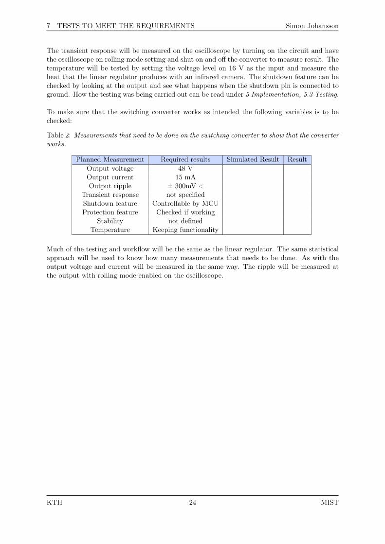
To make sure that the switching converter works as intended the following variables is to bechecked:
Table 2: Measurements that need to be done on the switching converter to show that the converterworks.
Planned Measurement Required results Simulated Result ResultOutput voltage 48 VOutput current 15 mAOutput ripple ± 300mV <
Transient response not specifiedShutdown feature Controllable by MCUProtection feature Checked if working
Stability not definedTemperature Keeping functionality
Much of the testing and workflow will be the same as the linear regulator. The same statisticalapproach will be used to know how many measurements that needs to be done. As with theoutput voltage and current will be measured in the same way. The ripple will be measured atthe output with rolling mode enabled on the oscilloscope.
KTH 24 MIST

8 IMPLEMENTATION Simon Johansson
8 Implementation
The following section will explain the work done to design the DC-DC converters. This includessimulations, PCB and which components that were bought. It explains why the values ondifferent components were chosen and shows the workflow of the simulations and the PCBcreation process.
8.1 Simulations
The program that was used for simulation the converters were LTspice IV[18]. LTspice is afreeware that Linear Technology has designed and already had simulation files finished on theirproducts. These simulation files simplified the work flow to simulate the power supplies as theintegrated ciruit were already in the library. Calculations made on the components were donein Mathematica 10.2.
8.1.1 Linear Converter
Simulation is needed to check that the LT3062 converter meets the voltage and current valuesbased on the choice of external components. From Linear Technology the following simulationwere given
Figure 17: Linear regulator with the correct values for 10 V output.
This is with the correct component values that I calculated. The voltage out is decided with
Vout = 0.6(1 +R2
R1)− (IADJ ∗R2) (14)
where IADJ is 15nA at 25 C[16]. Setting the output voltage to 10 V the unknown variablesis R2 and R1 which is used to set the output voltage. According to the datasheet, the valueof R1 should not be greater than 61.9kΩ for stability purposes. Choosing R1 to 47 kΩ we cannow solve the equation above with respect to R2. Leading to that R2 should be 737.2 kΩ. Theclosest resistance value according to international standard IEC 60063 is 750 kΩ. Input andoutput capacitance is recommended to 10 µF and be of the characteristic code X7R as thatcharacteristic have more stable dielectrics and can operate in a wider range of temperatures.The capacitor components must also be made of ceramics because of electrolytes do not workin a vacuum, they explode as the fluid freezes but are instead be sensitive to vibrations.
KTH 25 MIST
8 IMPLEMENTATION Simon Johansson
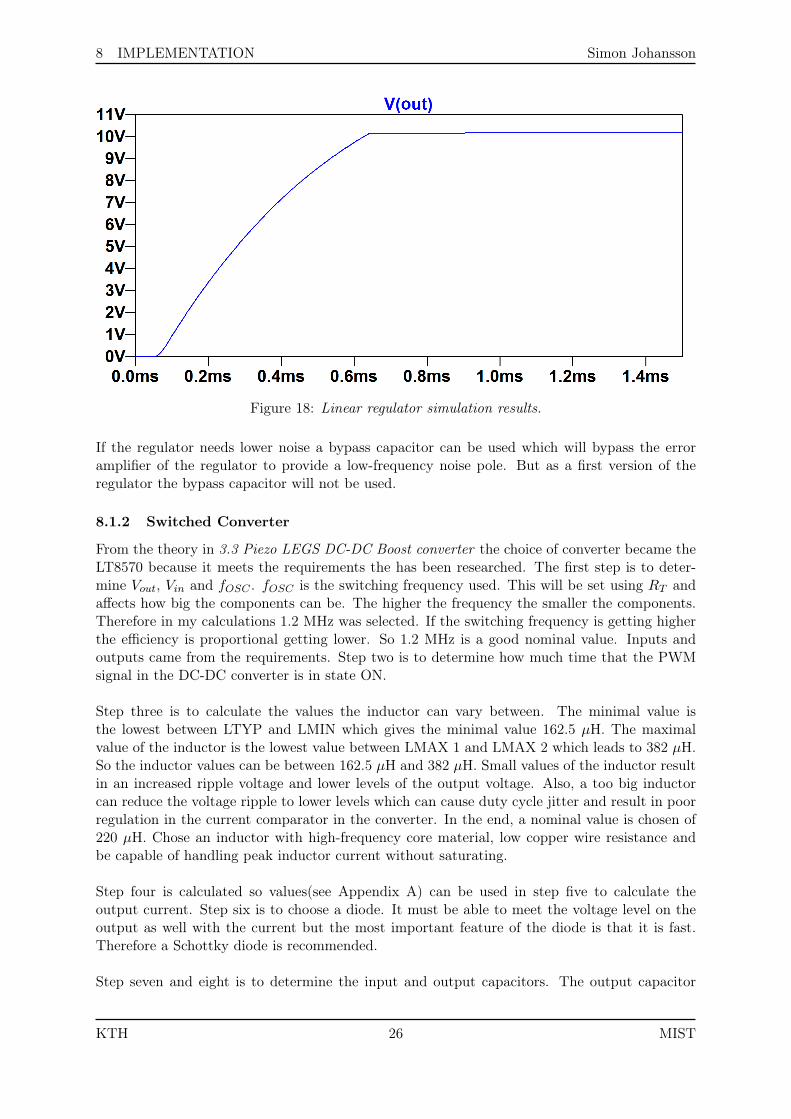
Figure 18: Linear regulator simulation results.
If the regulator needs lower noise a bypass capacitor can be used which will bypass the erroramplifier of the regulator to provide a low-frequency noise pole. But as a first version of theregulator the bypass capacitor will not be used.
8.1.2 Switched Converter
From the theory in 3.3 Piezo LEGS DC-DC Boost converter the choice of converter became theLT8570 because it meets the requirements the has been researched. The first step is to deter-mine Vout, Vin and fOSC . fOSC is the switching frequency used. This will be set using RT andaffects how big the components can be. The higher the frequency the smaller the components.Therefore in my calculations 1.2 MHz was selected. If the switching frequency is getting higherthe efficiency is proportional getting lower. So 1.2 MHz is a good nominal value. Inputs andoutputs came from the requirements. Step two is to determine how much time that the PWMsignal in the DC-DC converter is in state ON.
Step three is to calculate the values the inductor can vary between. The minimal value isthe lowest between LTYP and LMIN which gives the minimal value 162.5 µH. The maximalvalue of the inductor is the lowest value between LMAX 1 and LMAX 2 which leads to 382 µH.So the inductor values can be between 162.5 µH and 382 µH. Small values of the inductor resultin an increased ripple voltage and lower levels of the output voltage. Also, a too big inductorcan reduce the voltage ripple to lower levels which can cause duty cycle jitter and result in poorregulation in the current comparator in the converter. In the end, a nominal value is chosen of220 µH. Chose an inductor with high-frequency core material, low copper wire resistance andbe capable of handling peak inductor current without saturating.
Step four is calculated so values(see Appendix A) can be used in step five to calculate theoutput current. Step six is to choose a diode. It must be able to meet the voltage level on theoutput as well with the current but the most important feature of the diode is that it is fast.Therefore a Schottky diode is recommended.
Step seven and eight is to determine the input and output capacitors. The output capacitor
KTH 26 MIST
8 IMPLEMENTATION Simon Johansson
needs to withstand over 50 V. The input capacitor needs to withstand over 20 V. The calculatedvalue is 0.18 µF which is what the datasheet recommend. When looking at available vendorsthe closest value is 0.22 µF which in the end works for the simulation. Chose the same valueon the input as that is recommended in the datasheet. It is recommended that the capacitorsshould have as low of ESR(Equivalent series resistance) as possible to minimize the output ripplevoltage. Ceramic capacitors are preferred and they should be made of X7R dielectrics as thesematerials keep their capacitance over wider voltage and temperature ranges as well as to be ableto work in space. This, in turn, makes the capacitors sensitive to vibration so tests are neededfor make sure of their functionality.
Step nine is to set the output voltage level. This is done with a single resistance on the FBXpin. The calculation came up with 561.7 kΩ and after looking at the vendor the end value usedbecame 562 kΩ. The last step is to set the frequency the converter will switch. 1.2 MHz meansa resistance value of 70.25 kΩ.
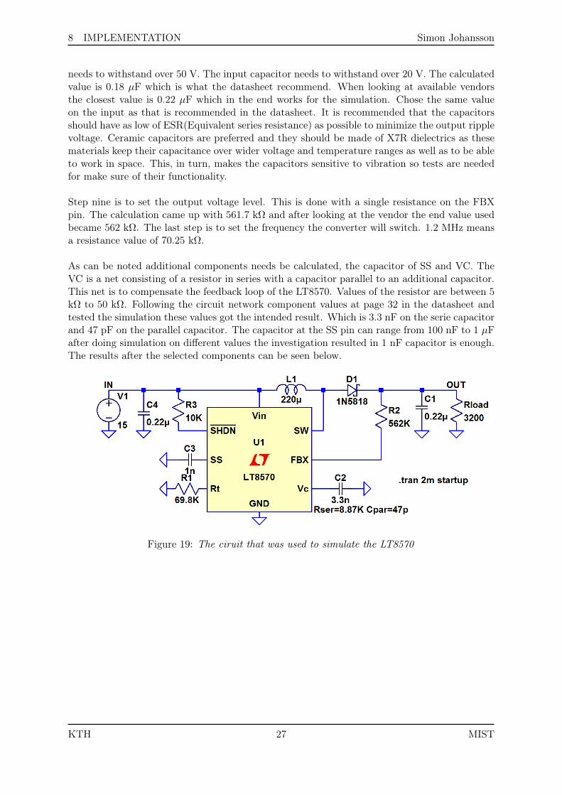
As can be noted additional components needs be calculated, the capacitor of SS and VC. TheVC is a net consisting of a resistor in series with a capacitor parallel to an additional capacitor.This net is to compensate the feedback loop of the LT8570. Values of the resistor are between 5kΩ to 50 kΩ. Following the circuit network component values at page 32 in the datasheet andtested the simulation these values got the intended result. Which is 3.3 nF on the serie capacitorand 47 pF on the parallel capacitor. The capacitor at the SS pin can range from 100 nF to 1 µFafter doing simulation on different values the investigation resulted in 1 nF capacitor is enough.The results after the selected components can be seen below.
Figure 19: The ciruit that was used to simulate the LT8570
KTH 27 MIST

8 IMPLEMENTATION Simon Johansson
Figure 20: The simulated result of the calculated values in the simulation
Figure 21: Output voltage and from this the ripple was calculated by taking the difference betweenthe highest and lowest value.
According to the simulation the circuit should work and such the work on the PCB began.
8.2 Printed Circuit Board(PCB)
8.2.1 Material & Program used
The program that was used to produce a schematic of the PCB was Diptrace. It was the programthat was used in another course at KTH so I have previous experience with how it works. ThePCB were then milled so I could measure the performance of the power supply.
KTH 28 MIST

8 IMPLEMENTATION Simon Johansson
8.2.2 Linear Converter
It is important to make sure that the converter is as small as possible and that the componentsare as close as possible to LT3062. The first pattern for the converter needed to be doneas Diptrace does not have the measurement of the converter. According to the datasheet ofLT3062, the footprint of the MS8E package is 3 × 3 mm. With the pins 3 × 4.90 mm. The nextstep is to connect the pins to a component that can be used in the schematic. This resulted inthe schematic below.
Figure 22: Schematic in Diptrace of the LT3062 converter that later is used to produce the PCB
The next thing is to make the PCB. To mill the PCB at KTH different kinds of mill rules neededto be applied. The mill rules came from Mark Smith from KTH. The minimum trace width is0.254 mm. The pins on an integrated circuit should therefore not be less than 0.254 mm widthapart. The trace should be at least 0.508 mm away from the edge of the board. The via holescan be:
• 0.5588 mm
• 0.7874 mm
• 0.8890 mm
• 0.9398 mm
• 1.0160 mm
• 3.1750 mm
KTH 29 MIST

8 IMPLEMENTATION Simon Johansson
The via holes had the recommended size of 1.778 mm with a 0.5588 mm hole in diameter. Thisis to make them easier to solder. The result of the PCB can be seen in Figure 23.
Figure 23: The final version of LT3062 PCB before it were milled.
The input from a power source shall be connected to Vin which then goes to the two inputs(pin6 and pin 5) on the integrated circuit. Pin 3 and pin 4 is the output that is connected to Vout.Both the input and output has decoupling capacitors to make the circuit more stable. Theoutput is connected to the 750 kΩ resistor which is connected to pin 2 called ADJ with anotherresistor of 47 kΩ to set the appropriate voltage level. SHDN is connected to the microcontrolleror a power source to turn on or off the regulator. Grounding this pin shuts off the regulator.The last pin 1 is the REF/BYP pin which is connected to a capacitor for reducing the outputnoise.
The goal was to keep the PCB as small and compact as possible with the components as closeto the regulator for minimizing the receptivity of disturbances and to see how small the regula-tor can become on the final PCB. The 10 kΩ resistance were added as a pull-down resistor formaking sure that the shutdown pin to be ground when the regulator is shut off.
8.2.3 Switched Converter
The LT8570 PCB have more restrictions and more EMC demands then the linear regulator. Italso has more external components and is more sensitive to how acceptable the soldering is. Inthe datasheet the following layout rules are recommended
• On the SW pin minimize the metal trace area connected to this pin to minimize EMI
• GND pad below the regulator must be soldered directly to local ground plane.
• It is recommended that there exists multiple vias in the printed circuit board to be usedto conduct heat away from the integrated circuit and into a copper plane with as mucharea as possible.
KTH 30 MIST
8 IMPLEMENTATION Simon Johansson
• The VC and FBX components should be kept as far away as practical from the switchnode, while still remaining close to the chip. The ground for these components should beseparated from the switch current path
• The loop between Vin, the inductor and the SW pin to ground should be kept as short aspossible because it reduces the parasitic trace inductance and noise.
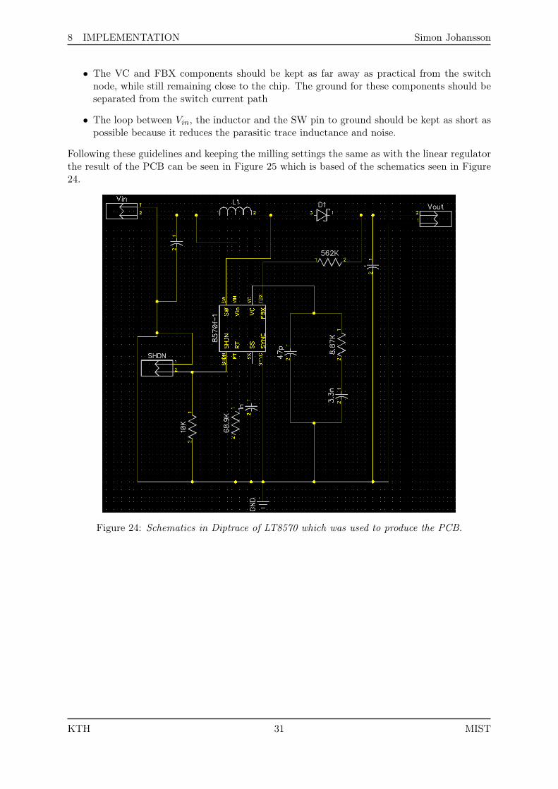
Following these guidelines and keeping the milling settings the same as with the linear regulatorthe result of the PCB can be seen in Figure 25 which is based of the schematics seen in Figure24.
Figure 24: Schematics in Diptrace of LT8570 which was used to produce the PCB.
KTH 31 MIST

8 IMPLEMENTATION Simon Johansson
Figure 25: The final version of the PCB layout
It can be noted that both the integrated circuit(the converter) and the inductor had their pat-terns done to fit the PCB. Meaning that their patterns needed to be done in reference to theirdatasheets. The integrated circuit of LT8570 was made to be around 5 mm in height and 3 mmin width. For the inductor, the footprint was made a little larger to make it easier to solder.
The components of the PCB is placed as close as possible and tries to meet the recommendedlayout defined in the datasheet. The thickness of the tracers was bigger as the voltage level ishigher. The FBX resistor was as close as possible to the integrated circuit and still close to theoutput. The SW pin is as close as possible to the integrated circuit to make the EMC loop asshort as possible and the ground is separated from the rest of the circuit as recommended.
8.3 Purchase of components
The components that needs to be purchased is 7 capacitors, 6 resistors, a diode, an inductorand the two converters. The recommended vendor that were used was Farnell. They have manydifferent components and their delivery time is very short. The things to consider when buyingthe capacitors is
• Enough voltage level
• Solder size. As we solder it ourselves 0603 is a good size
• The material that the capacitor is made of. The capacitor is recommended to be made ofceramic and have dielectics of X7R
• To withstand the temperature variation from in the environment which will be no problemas the temperature is so low. The normal -40 to 125 degrees Celsius is enough
• Must be surface mountable
KTH 32 MIST

8 IMPLEMENTATION Simon Johansson
Following these criteria the capacitors chosen can be seen in the table 3.
Table 3: Capacitors purchased for the two converters
Experiment Value Size Operating temperature Rated voltage Order codeSiC 10µF 1206 -55 to 125C 25V 1828837SiC 1nF 0603 -55 to 125C 50V 2496824Piezo 0.22µF 0603 -55 to 125C 25V 1414626Piezo 0.22µF 0805 -55 to 125C 50V 8820139Piezo 3.3nF 0805 -55 to 125C 25V 1856458Piezo 47pF 0805 -55 to 125C 25V 1414692Piezo 1nF 0805 -55 to 125C 50V 8819955
The resistors main characteristics that were looked at is size, resistance tolerance at 1% anda maximum working voltage of 50V. Size 0603 were selected as lower is hard to solder. Thetolerance was set to 1% because the FBX and ADJ resistors need to have exact values so theoutput voltage is correct. The 50 V is to meet the requirement of the 48 V output of the Piezoconverter.
Table 4: Resistors purchased for the two converters
Experiment Value Size Resistance material Rated voltage Order codeSiC 47kΩ 0603 thick film 50V 9331255
SiC & Piezo 10kΩ 0603 thick film 50V 2447230SiC 750kΩ 0603 thick film 50V 9331530Piezo 8.87kΩ 0603 thick film 50V 1170885Piezo 69.8kΩ 0603 thick film 50V 1170972Piezo 562kΩ 0603 thick film 50V 1171061
The inductor is recommended to have high-frequency core material such as ferrite, more volumefor a given inductance, low copper wire resistance(DCR) and use a toroidal or shielded induc-tor. The high-frequency core material helps to reduce core losses and the volume for a giveninductance which improves the efficiency of the inductor.
Table 5: Inductor purchased for the switch-mode regulator
Experiment Value Saturation Power Efficient Power Value Order codePiezo 220µH 360mA 450mA 2408301
The recommended diode is a diode with low forward-voltage drop and fast switching speeds andis able to handle an average forward current of 1A. Schottky diode is meets this criteria. Theone used in this application can be seen in table 6.
Table 6: Diode purchased for the switch converter
Experiment Type Reverse voltage Forward voltage Order codePiezo Schottky 60V 630mV 9525076
The choice of converters has been motivated in Choosing a power supply for space application.
KTH 33 MIST
8 IMPLEMENTATION Simon Johansson
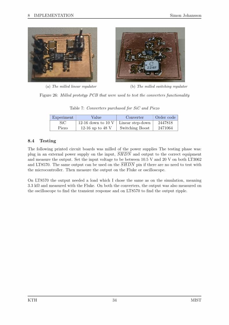
(a) The milled linear regulator (b) The milled switching regulator
Figure 26: Milled prototyp PCB that were used to test the converters functionality
Table 7: Converters purchased for SiC and Piezo
Experiment Value Converter Order codeSiC 12-16 down to 10 V Linear step-down 2447818Piezo 12-16 up to 48 V Switching Boost 2471064
8.4 Testing
The following printed circuit boards was milled of the power supplies The testing phase was:plug in an external power supply on the input, SHDN and output to the correct equipmentand measure the output. Set the input voltage to be between 10.5 V and 20 V on both LT3062and LT8570. The same output can be used on the SHDN pin if there are no need to test withthe microcontroller. Then measure the output on the Fluke or oscilloscope.
On LT8570 the output needed a load which I chose the same as on the simulation, meaning3.3 kΩ and measured with the Fluke. On both the converters, the output was also measured onthe oscilloscope to find the transient response and on LT8570 to find the output ripple.
KTH 34 MIST

9 RESULTS Simon Johansson
9 Results
9.1 SiC results
LT3062 linear converter obtained the calculated values and was measured with 99% confidenceinterval. The 25 point measurements of the output of the LT3062 were all the same when theinput was varied between 10 V and 20 V. Lower input than 10.2 meant that the converter didnot work as intended. The measured output was 10.175 which gives us the expectation value of
x =1
n
n∑k=1
xk =1
25
25∑k=1
10.177k ⇒ x = 10.168 (15)
and the variation
σ2 = s2 =1
25− 1
25∑k=1
(10.177k − 132.301)2 ⇒ s2 = 5610.11⇒ s = σ = 0.374166 ∗ 103 (16)
The quantile is
q =1 + 0.99
2= 0.995⇒ q0.995 = 2.79694
gives n asCIµ = x± q0.995
σ√n⇒ n = 42.7813 (17)
After calculating the number of measurements needed for making sure that the measurementsis 99% accurate the following result can be read in table 8.
Table 8: Final result of the performance of the linear converter LT3062.
Measurement Required results Simulated Result ResultOutput voltage 10 V 10.166 V 10.175 VOutput current 200 mA 10 mA 8 mA
Transient response 10µs > 8ms 80 msShutdown feature Controllable with MCU
√ √
Protection feature Working feature X XTemperature Functional between -30 to 100C CNBS* XTable 9: CNBS=Can Not Be Simulated. X meaning that the test was not done.
KTH 35 MIST

9 RESULTS Simon Johansson
Figure 27: The transient response of LT3062.
There was enough time to produce a PCB for the entire SiC experiment for testing the fullfunctionality of the experiment together with LT3062. This meant that the LT3062 was testedwith the measuring circuit and microcontroller to check the performance of the first prototype.This can be seen below.
Figure 28: Final prototype PCB of the whole SiC experiment. LT8570 is not applied on thisversion of PCB.
The following power consumption was measured on the prototype. This is without the SiCtransistors as they did not arrive under this thesis work.
KTH 36 MIST
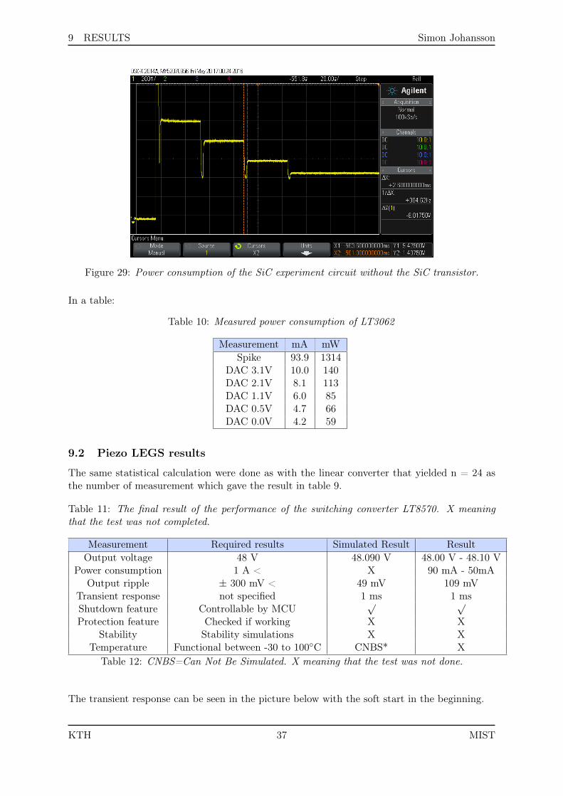
9 RESULTS Simon Johansson
Figure 29: Power consumption of the SiC experiment circuit without the SiC transistor.
In a table:
Table 10: Measured power consumption of LT3062
Measurement mA mWSpike 93.9 1314
DAC 3.1V 10.0 140DAC 2.1V 8.1 113DAC 1.1V 6.0 85DAC 0.5V 4.7 66DAC 0.0V 4.2 59
9.2 Piezo LEGS results
The same statistical calculation were done as with the linear converter that yielded n = 24 asthe number of measurement which gave the result in table 9.
Table 11: The final result of the performance of the switching converter LT8570. X meaningthat the test was not completed.
Measurement Required results Simulated Result ResultOutput voltage 48 V 48.090 V 48.00 V - 48.10 V
Power consumption 1 A < X 90 mA - 50mAOutput ripple ± 300 mV < 49 mV 109 mV
Transient response not specified 1 ms 1 msShutdown feature Controllable by MCU
√ √
Protection feature Checked if working X XStability Stability simulations X X
Temperature Functional between -30 to 100C CNBS* XTable 12: CNBS=Can Not Be Simulated. X meaning that the test was not done.
The transient response can be seen in the picture below with the soft start in the beginning.
KTH 37 MIST
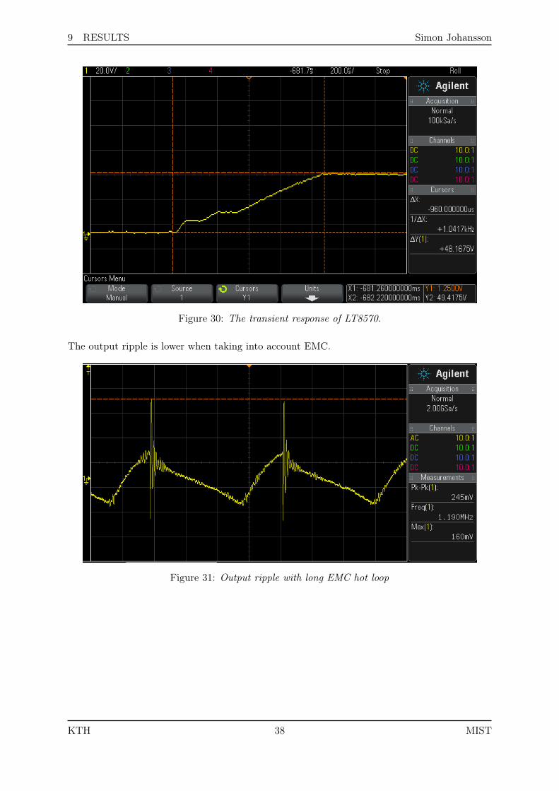
9 RESULTS Simon Johansson
Figure 30: The transient response of LT8570.
The output ripple is lower when taking into account EMC.
Figure 31: Output ripple with long EMC hot loop
KTH 38 MIST

9 RESULTS Simon Johansson
Figure 32: Output ripple with short EMC hot loop
KTH 39 MIST

10 DISCUSSION Simon Johansson
10 Discussion
The choice of the converters was the most important assignment to solve. This work gave theintended result with both power supply reaching their demands. One reason to use anotherpower supply is that there is more space on the SiC PCB. To make LT8570 a better solution isto research how it would perform in the Sepic configuration. Because this would keep the PiezoLEGS motor more safe as there are no current flowing through to the output when LT8570 isshut down.
There are important considerations when producing a PCB. A bad layout will decrease theperformance of the converter substantially, especially LT8570 that is more sensitive of bad PCBlayout because of the PWM switching can lead to instability. The difference is quite big betweenthe two LT8570 PCB which were compared with each other. Keeping this layout is importanton the final SiC experimental PCB. The linear converter LT3062 is straightforward as there arenot oscillating components inherent in the design. This means that the traces on the PCB is notin danger of interference from other sources that otherwise could affect the converter. Thereforethe PCB is easy to produce and the result has a high success rate which was the reason to chosea linear converter.
The PCB of the switching converter LT8570 is more advanced with respect to the design. Itrequires closer tracers for SW, diode and output capacitor as the EMC will be worse if thatloop is not as short as possible. Keeping EMC low it is required that the soldering shall beclean. Two PCB prototypes did not work because of that the ground underneath LT8570 wasnot soldered correctly. More research needs to be a consideration on the heat dissipation asthis was not tested enough. More research is needed on EMC as well. The PCB prototype onLT8570 did not have a cancellation layer for EMI. This will be needed on the finalization of thePCB. In that sense, it is important that the final PCB product is made of four layers so therecan be a separate layer of power, ground and one for the EMC hot loop. This will minimize thenoise and help with heat dissipation.
The choice of components will affect the performance of converters if chosen carelessly. Theresults of the regulator may be better if the values of the components do not fluctuate. Keepingthem at a maximum error of 1% is the lowest we can go. Otherwise, important components,such the ADJ resistors on the LT3062 and the FBX resistor on the LT8570 will be affected sothe output voltage level can be erroneous. The components worked well in this conditions. ButLT8570 needs more capacitor according to Piezo LEGS.
The methods used to implement this project worked well. It was important to do the pilotstudy thoroughly because it helped in the selection of the correct power supply. A bad pilotstudy had been able to make the outcome worse by choosing a converter that may not haveperformed as well as the one chosen now. The protection feature was not tested as there wasnot enough time to test it. The possibility that the power supply was destroyed would not haveworked with this timetable. Temperature tests could not be carried out as the test environmentto reach high temperature is not conceivable and an infrared camera was not present at KTH.The PCB prototype would not survive if heated as the material that was used when we did themilling were sensitive to prolonged heat exposure. Therefore, a more heat-resistant PCB designmade of a heat-resistant material needs to be checked so the converters can be tested in a widertemperature range. The internal protection of the two converters could not be tested enoughto meet the requirements, this is something to be researched in future work. Same with thestability loop of LT8570.
KTH 40 MIST
11 FUTURE WORK Simon Johansson
11 Future work
The power supplies need more testing for confirming that the power supplies keep their function-ality even after been exposed to extreme environments. On the spaceflight, the converters willbe facing vibration, hot and cold temperature, radiation, current, vacuum and voltage spikesand heat dissipation issues. It is, therefore, crucial to producing more advanced testing environ-ments to test the functionality of the power supply even when exposed to these hazards. Doingresearch on how to find these test environments and variables is a crucial part of future work.
The PCB of the LT8570 may need another critical eye and more stability testing over a longerperiod of time to make sure it is working as intended and that the EMC loops are not affectingthe performance of the power supply. Simulations of the stability also is needed for further ver-ification that LT8570 is stable. This can then be extended to the finalization of the SiC PCB.It needs an update as the trace routing is not ideal and the placement of the different parts ofthe PCB is not optimal.
LT8570 needs additional radiation testing of both magnetic-field and EMI to make sure thatthe EMI from it is not high. It should not be able to affect other experiments. This must bemeasured so the MIST team know what the SiC and Piezo team are radiating. This report didnot have the time to get tools to measure the EMI, this is something to investigate in futurereports.
The environment that the satellite is located in affect the functionality of the power supplyand the material they are made of. An example of this is the atomic oxygen which is pure oxy-gen that exists in the atmosphere which is responsive to organic materials. This is somethingthat the MIST team may already be investigated but that this thesis has not been able to find.Research on these effects needs future investigation and can be a part of the future work. Asmentioned in the results a more comprehensive testing of the performance in a wider range oftemperature needs to be performed as now the only temperature that the power supply has beentested in is around 18 degrees Celsius.
Vibration tests are needed to know if all the components on the PCB is capable of withstandingthe vibration that is introduced when the rocket is launching. Heat dissipation needs to betested both on earth as well in vacuum and over a long period of time to make sure that thePCB is not getting overheated or destroyed and to make sure that the performance is good evenif there is big variations of temperature.
Keeping resistors and capacitors voltage tolerance on LT8570 at 50 V is to low. It will benecessary to buy components that have 75 V voltage tolerance on the final PCB. Piezo LEGSwants more output capacitors. This is something that needs to be investigated further.
Both of the converters needs a fuse which this thesis have not looked into. The MIST teamhave a ready solution but that needs to be tested together with the regulators and with therest of the SiC experimental PCB. The protection features of the power supplies needs furthertesting.
KTH 41 MIST

12 CONCLUSIONS Simon Johansson
12 Conclusions
The information provided in this report gives enough information to know how a power supplyworks and goes through the workflow on how to implement two converters based on the require-ments of the experiment. Both of the converters has been tested and have met this requirementas a stand alone and is ready for future testing and implementation to the final PCB to SiC. TheLT3062 converter has been tested on the SiC experiment and is working as intended. LT8570needs more testing against the Piezo LEGS experiment. Much testing is needed for finalizingthe power supply for keeping the functionality over the long term for which the satellite will bein space.
KTH 42 MIST

REFERENCES Simon Johansson
References
[1] MIST-Team. (Mar. 30, 2016). Basic facts, [Online]. Available: https://mistsatellite.wordpress.com/basic-facts/.
[2] ——, (Apr. 18, 2016). Piezo legs, [Online]. Available: https://www.kth.se/en/sci/centra/rymdcenter/studentsatellit/piezo-legs-1.525050.
[3] ——, (Mar. 30, 2016). Sic in space, [Online]. Available: https://www.kth.se/sci/centra/rymdcenter/studentsatellit/sic-in-space-1.525052.
[4] M. Östling. (Mar. 30, 2016). Wov – working on venus, [Online]. Available: https://www.kth.se/blogs/wov/.
[5] H. Klinkrad, Space debris. Wiley Online Library, 2010.
[6] G. Drolshagen, “Impact effects from small size meteoroids and space debris,” Advances inspace Research, vol. 41, no. 7, pp. 1123–1131, 2008.
[7] B. R. Babu, A. K. Parande, and C. A. Basha, “Electrical and electronic waste: A globalenvironmental problem,” Waste Management & Research, vol. 25, no. 4, pp. 307–318, 2007.
[8] H. Paulsson and M. André, “Design of microcontroller circuit and measurement software forsic and morebac experiment,” in. KTH Royal Institute of Technology, Stockholm, TRITA-ICT-EX-2016:38, 2016.
[9] M. Ericson and J. Silverudd, “Design of measurements circuits for sic experiment, kthstudent satellite mist,” in. KTH Royal Institute of Technology, Stockholm,TRITA-ICT-EX-2016:37, 2016.
[10] M. K. Kazimierczuk, “Introduction,” in Pulse-Width Modulated DC-DC Power Convert-ers. John Wiley & Sons, Ltd., 2008, pp. 1–22, isbn: 9780470694640. doi: 10 . 1002 /9780470694640.ch1. [Online]. Available: http://dx.doi.org/10.1002/9780470694640.ch1.
[11] ——, “Boost pwm dc-dc converter,” in Pulse-Width Modulated DC-DC Power Convert-ers. John Wiley & Sons, Ltd., 2008, pp. 85–137, isbn: 9780470694640. doi: 10.1002/9780470694640.ch3. [Online]. Available: http://dx.doi.org/10.1002/9780470694640.ch3.
[12] B. Molin, Analog Elektronik. Studentlitteratur, 2009, pp. 430–460, isbn: 978-91-44-05367-7.
[13] Linear Technology. (May 10, 2016). Basic concepts of linear regulator and switching modepower supplies, [Online]. Available: http://cds.linear.com/docs/en/application-note/AN140fa.pdf.
[14] M. K. Kazimierczuk, “Buck pwm dc-dc converter,” in Pulse-Width Modulated DC-DCPower Converters. John Wiley & Sons, Ltd., 2008, pp. 23–83, isbn: 9780470694640. doi:10.1002/9780470694640.ch2. [Online]. Available: http://dx.doi.org/10.1002/9780470694640.ch2.
[15] Linear Technology. (Jun. 3, 2016). Power supply layout and emis, [Online]. Available:http://cds.linear.com/docs/en/application-note/an139f.pdf.
[16] ——, (Jun. 3, 2016). Lt3062 datasheet, [Online]. Available: http://cds.linear.com/docs/en/datasheet/3062f.pdf.
[17] ——, (Jun. 3, 2016). Lt8570 datasheet, [Online]. Available: http://cds.linear.com/docs/en/datasheet/85701f.pdf.
KTH 43 MIST

REFERENCES Simon Johansson
[18] ——, (Jun. 3, 2016). Design simulation and device models, [Online]. Available: http://www.linear.com/designtools/software/.
KTH 44 MIST

Calculation LT8570 for simulation 1.0Calculations on LT8570 for finding the correct components to meet the requirements
Step 1: Inputs
In[1]:=
VinMIN = 14;(*Minimal battery voltage from CubeSat*)
VinMAX = 16;(*Maximal battery voltage from CubeSat*)
Vout = 48;(*Voltage that the Piezo LEGS motor needs*)
Iout = 15 * 10-3;(*Minimal battery current to Piezo Motor*)
Fosc = 1.2 * 106;
(*Is the switching frequency: Choose different values to test out*)
IRTYP = 75 * 10-3;(*150mA for LTC8570 and 75mA for LT8570-1*)
Ksc = 0.3;(*kSC=0.6A for LT8570 and 0.3A for LT8570-1*)
Irmin = 0.02;(*0.04A for LT8570 and 0.02A for LT8570-1*)
Ilim = 0.25;(*0.5A for LT8570 and 0.25A for LT8570-1*)
Reference: http://cds.linear.com/docs/en/datasheet/85701f.pdf
Step 2: DC
DC ≈ Vout -Vin+VDVout+VD+VCEAST
In[10]:= DCMAX =Vout - VinMIN + 0.5
Vout + 0.5 - 0.4// N
Out[10]= 0.717256
In[11]:= DCMIN =Vout - VinMAX + 0.5
Vout + 0.5 - 0.4// N
Out[11]= 0.675676
Step 3: L
In[12]:= LTYP =VinMIN - 0.4 * DCMAX
Fosc * IRTYP
Out[12]= 0.000108385
In[13]:= LMIN =VinMIN - 0.4 * 2 * DCMAX - 1
Ksc * DCMAX - 300 * 10-9 * Fosc * Fosc * 1 - DCMAX// N
Out[13]= 0.000162504
Printed by Wolfram Mathematica Student Edition
A APPENDIX : COMPONENT CALCULATIONS Simon Johansson
A Appendix : Component calculations
KTH 45 MIST

In[14]:= LMAX1 =VinMIN - 0.4 * DCMAX
Fosc * Irmin
LMAX2 =VinMIN - 0.4 * DCMIN
Fosc * Irmin
Out[14]= 0.000406445
Out[15]= 0.000382883
Step 4: Iripple
In[16]:= IRIPPLEMIN =VinMIN - 0.4 * DCMAX
Fosc * LMIN
IRIPPLEMAX =VinMAX - 0.4 * DCMIN
Fosc * LMIN
Out[16]= 0.0500227
Out[17]= 0.0540527
Step 5: Iout
In[18]:= IOUTMIN = Ilim -IRIPPLEMIN
2* 1 - DCMAX
IOUTMAX = Ilim -IRIPPLEMAX
2* 1 - DCMIN
Out[18]= 0.0636143
Out[19]= 0.0723158
Step 6:D1
Gives
VR > VOUT; IAVG > IOUT
VR > 48 V ; IAVG > 15mA
Step 7: Cout
In[20]:= COUT =IOUTMAX * DCMAX
Fosc * 0.005 * Vout
Out[20]= 1.801 × 10⁻⁷
Step 8: Cin
In[21]:=Ilim * DCMAX
40 * Fosc * 0.005 * VinMIN+
IRIPPLEMAX
8 * Fosc * 0.05 * VinMAX
Out[21]= 6.04053 × 10⁻⁸
2 CalculationsLTC8570.nb
Printed by Wolfram Mathematica Student Edition
46

Step 9: RFBX
In[22]:= RFBX =Vout - 1.204
83.3 * 10-6
Out[22]= 561777.
Steo 10 :RT
In[23]:= RT =85.5Fosc
106
- 1
Out[23]= 70.25
CalculationsLTC8570.nb 3
Printed by Wolfram Mathematica Student Edition
47

TRITA TRITA-ICT-EX-2016:36
www.kth.se