design of synchronization subsystem for an ultra wideband
TRANSCRIPT

Design of Synchronization Subsystem for an Ultra
Wideband Radio
by
Raul Blazquez-Fernandez
Submitted to the Department of Electrical Engineering and ComputerScience
in partial fulfillment of the requirements for the degree of
Master of Science in Electrical Engineering and Computer Science
at the
MASSACHUSETTS INSTITUTE OF TECHNOLOGY
May 2003
@Massachusetts Institute of Technology. All rights reserved.
Author .... .... . -:
Department of Electrical Engineering and Computer ScienceMay 9, 2003
Certified by...............Anantha P. Chandrakasan
Associate ProfessorThesis Supervisor
Accepted by...Artl ur C. Smith
Chairman, Department Committee on Graduate Students
BARKER
MASSACHUSETTS INSTITUTEOF TECHNOLOGY
JUL 0 7 2003
LIBRARIES

2

Design of Synchronization Subsystem for an Ultra Wideband
Radio
by
Raul Blazquez-Fernandez
Submitted to the Department of Electrical Engineering and Computer Scienceon May 9, 2003, in partial fulfillment of the
requirements for the degree ofMaster of Science in Electrical Engineering and Computer Science
Abstract
Ultra Wideband (UWB) systems are receiving recently more attention due to itsapproval by FCC. The systems that have been already implemented are based inanalog correlation. This thesis is part of an effort to implement a wholly digital UltraWideband receiver. Synchronization of a signal is a first step to perform the correctdemodulation of the data contained in it. It is a problem whose complexity doesnot scale linearly with the bandwidth of the received signal. In UWB bandwidths areover 1 GHz, and the synchronization process has an important impact in the overheadneeded in each data packet compared to the amount of information. In this thesis,the synchronization subsystem of an all digital UWB receiver is designed, taking intoaccount the specific properties of UWB signals.
Thesis Supervisor: Anantha P. ChandrakasanTitle: Associate Professor
3

4

Acknowledgments
I would like to thank Prof. Anantha Chandrakasan, for giving me the opportunity
of working in this hectic and interesting area, and teaching me to look with different
eyes to what I knew in signal processing, while providing the best foundation and
guidance to explore the area of digital circuit design, completely new to me. His
encouragement and patience have been essential for the completion of this thesis. I
consider myself lucky for working with such a prominent leader in the field of circuits
and systems.
I would like to thank Puneet Newaskar and Fred Lee of the UWB, wonderful
friends and colleagues, for their support and patience. Working with them has been
an enriching experience, both professionally and personally. Their sense of humor,
attitude, confidence, and the many conversations have made this time really interest-
ing.
Many thanks to the Digital Integrated Circuits and Systems group, both present
and graduated students Manish Bhardwaj, Alice Wang, Rex Min, Theodoros Kon-
stantakopoulos, Johnna Powell, Alexandra Kern, Julia Cline, Dave Wentzloff, Ben
Calhoun, Travis Simpkins, Frank Honore, SeongHwan Cho, Nathan Ickes. They
make the group a great place to be. Their friendship and help are greatly appreci-
ated. I also would like to thank Margaret Flaherty, our administrative assistant, for
her skilled support.
I would also like to thank La Caixa Fellowship Program, for the opportunity they
gave me to pursue my research interests abroad. Their efficient management of the
different stages of the fellowship makes it one of the best possible ways of starting
graduate studies in an American university. This research has also been sponsored
by Hewlett-Packard under the HP/MIT Alliance.
Finally, I would like to thank my parents, Magdalena and Felix, for so many things
that would not fit neither in one, nor in a hundred pages. Thank you for everything.
Finalmente, me gustaria dar gracias a mis padres, Magdalena and Felix, por tantas
cosas que no cabrian ni en una ni en cien paginas. Gracias por todo.
5

6

Contents
1 Introduction
1.1 UW B signal ................
1.1.1 Time representation . . . . . . .
1.1.2 Frequency representation . . . . .
1.1.3 Advantages of UWB systems . . .
1.2 Previous work . . . . . . . . . . . . . . .
1.2.1 A CDMA receiver . . . . . . . . .
1.2.2 UWB receiver, analog correlation
1.2.3 UWB receiver, digital correlation
1.3 Objectives of the thesis . . . . . . . . . .
1.3.1 Assumptions . . . . . . . . . . . .
1.3.2 Tracking algorithm . . . . . . . .
1.3.3 Structure of the thesis . . . . . .
2 Coarse acquisition
2.1 Coarse acquisition algorithm . . . . . . . . . . . . . . . . . . . . . . .
2.1.1 Matched filter : Adaptation to a simple integration window . .
2.1.2 Definition of Pd and Pf . . . . . . . . . . . . . . . . . . . . ..
2.1.3 Specification of the value of D . . . . . . . . . . . . . . . . . .
2.2 Definition of the coarse acquisition process as a discrete stochastic process
2.2.1 Coarse acquisition as a Markov chain . . . . . . . . . . . . . .
2.2.2 Mathematical characterization of the model for coarse acquisition
2.2.3 Generalization of results when parallel architectures are possible
7
17
. . . . . . . . . . . . . . 18
. . . . . . . . . . . . . . 18
. . . . . . . . . . . . . . 2 3
. . . . . . . . . . . . . . 24
. . . . . . . . . . . . . . 27
. . . . . . . . . . . . . . 2 7
. . . . . . . . . . . . . . 30
. . . . . . . . . . . . . . 32
. . . . . . . . . . . . . . 33
. . . . . . . . . . . . . . 3 3
. . . . . . . . . . . . . . 34
. . . . . . . . . . . . . . 36
39
39
43
45
46
49
50
52
55

2.3 Effect of a difference in frequency between clocks . . . .
2.3.1 Conventions and models . . . . . . . . . . . . . .
2.3.2 Non-idealities of the estimator . . . . . . . . . . .
2.4 Sum m ary . . . . . . . . . . . . . . . . . . . . . . . . . .
3 Fine Tracking
3.1 Necessity of a fine tracking algorithm . . . . . . . . . . .
3.2 A nalysis . . . . . . . . . . . . . . . . . . . . . .
3.2.1 Model of the system after coarse synchror
3.2.2 Effect of a frequency offset . . . . . . . .
3.2.3 Effect of a delay difference . . . . . . . .
3.2.4 Effect of random noise . . . . . . . . . .
3.2.5 Choice of the coefficients of the filter . .
3.3 Definition of the delay estimator . . . . . . . . .
3.3.1 Impact of AWGN . . . . . . . . . . . . .
3.3.2 Impact of difference of frequencies . . . .
3.3.3 Impact of the granularity of the division
3.3.4 Granularity of the corrections . . . . . .
3.4 Specification of the total jitter of the system . .
3.5 Sim ulation . . . . . . . . . . . . . . . . . . . . .
3.6 Sum m ary . . . . . . . . . . . . . . . . . . . . .
4 Implementation
4.1 Characteristics of the signal . . . . . . . . . . .
4.2 Modes of operation of the receiver . . . . . . . .
4.3 General block diagram . . . . . . . . . . . . . .
4.4 Digital Front-end . . . . . . . . . . . . . . . . .
4.4.1 Buffers . . . . . . . . . . . . . . . . . . .
4.4.2 Control for the Digital Front-end . . . .
4.5 Back-end subsystem . . . . . . . . . . . . . . .
4.5.1 Correlation subsystem . . . . . . . . . .
. . . . . . . . . . . . 6 7
ization . . . . . . . 67
. . . . . . . . . . . . 7 0
. . . . . . . . . . . . 7 1
. . . . . . . . . . . . 7 2
. . . . . . . . . . . . 7 2
. . . . . . . . . . . . 7 3
. . . . . . . . . . . . 7 4
. . . . . . . . . . . . 7 6
. . . . . . . . . . . . 7 6
. . . . . . . . . . . . 7 9
. . . . . . . . . . . . 7 9
. . . . . . . . . . . . 8 1
. . . . . . . . . . . . 8 1
83
. . . . . . . . . . . . 8 3
. . . . . . . . . . . . 8 4
. . . . . . . . . . . . 8 5
. . . . . . . . . . . . 8 8
. . . . . . . . . . . . 8 8
. . . . . . . . . . . . 9 0
. . . . . . . . . . . . 9 2
. . . . . . . . . . . . 9 2
8
. . . . . 56
. . . . . 56
. . . . . 59
. . . . . 63
65
. . . . . 65

4.5.2 Fine tracking . . . . . . . . . . . . . . . . . . . . . . . . . . . 95
4.5.3 Coarse acquisition subsystem . . . . . . . . . . . . . . . . . . 98
4.6 Implementation of the delay adjustment . . . . . . . . . . . . . . . . 103
4.6.1 Required functionality . . . . . . . . . . . . . . . . . . . . . . 103
4.6.2 State machine for implementing the change in delay . . . . . . 106
4.6.3 Implementation of the Swapper . . . . . . . . . . . . . . . . . 108
4.7 Interface of the receiver . . . . . . . . . . . . . . . . . . . . . . . . . . 108
4.8 Sum m ary . . . . . . . . . . . . . . . . . . . . . . . . . . . . . . . . . 110
5 Conclusions 113
5.1 Future work . . . . . . . . . . . . . . . . . . . . . . . . . . . . . . . . 114
9

10

List of Figures
Baseband pulses. . . . . . . . . . . . . . . . . . . . . . . . . . . . . . 19
W avelet pulses . . . . . . . . . . . . . . . . . . . . . . . . . . . . . . . 20
UWB encoding of 1 and 0 . . . . . . . . . . . . . . . . . . . . . . . . 22
Frequency spectrum associated to different pulse shapes. . . . . . . . 24
Frequency spectrum associated to a gold code example. . . . . . . . . 25
Multipath in a narrowband signal. . . . . . . . . . . . . . . . . . . . . 27
Multipath in a UWB signal. . . . . . . . . . . . . . . . . . . . . . . . 28
Correlator channel in a CDMA receiver. . . . . . . . . . . . . . . . . 29
Architecture of UWB receiver with analog correlation . . . . . . . . . 30
Structure of a doublet. . . . . . . . . . . . . . . . . . . . . . . . . . . 31
Architecture of UWB receiver by Berkeley Wireless Research Center. 32
Coarse acquisition algorithm. . . . . . . . . . . . . . . . . . . . . . . 35
Fine tracking algorithm. . . . . . . . . . . . . . . . . . . . . . . . . . 35
1-1
1-2
1-3
1-4
1-5
1-6
1-7
1-8
1-9
1-10
1-11
1-12
1-13
2-1
2-2
2-3
2-4
2-5
2-6
2-7
2-8
41
41
42
43
45
47
47
48
11
Matched filter concept . . . . . . . . . . . . . . . . . . . . . . . .
Correlation obtained by multiplication with a template . . . . . .
Received signal and possible templates . . . . . . . . . . . . . . .
D etail of Figure 2-3 . . . . . . . . . . . . . . . . . . . . . . . . . .
Relation of SNRs in function of the relation between W and V . .
Pfa with absolute value. . . . . . . . . . . . . . . . . . . . . . . .
Pfa with the threshold as parameter. . . . . . . . . . . . . . . . .
Probability of detection with the ratio Thla as parameter. . . . .

2-9 Loss in Signal to Noise Ratio due to misalignment of the integration
w indow . . . . . . . . . . . . . . . . . . . . . . . . . . . . . . . . . . . 48
2-10 Situation of two consecutive windows for coarse acquisition considera-
tion s. . . . . . . . . . . . . . . . . . . . . . . . . . . . . . . . . . . . . 49
2-11 Pd in one of the two integration windows where part of the pulse is
present as a function of D. . . . . . . . . . . . . . . . . . . . . . . . . 50
2-12 Coarse acquisition as a Markov process. . . . . . . . . . . . . . . . . . 51
2-13 Notation on the pulse position estimation . . . . . . . . . . . . . . . . 57
2-14 Maximum frequency deviation for starting to have SNR loss as a func-
tion of position r. . . . . . . . . . . . . . . . . . . . . . . . . . . . . . 61
2-15 Change of probability of detection due to a difference in frequencies
between transmitter and receiver . . . . . . . . . . . . . . . . . . . . 64
3-1 Fine tracking block diagram . . . . . . . . . . . . . . . . . . . . . . . 67
3-2 Timing references for the Delay Locked Loop . . . . . . . . . . . . . . 68
3-3 Fine tracking block diagram, interpretation . . . . . . . . . . . . . . . 69
3-4 Spectrum of error noise depending on the value of b . . . . . . . . . . 73
3-5 Estimation of the delay with a frequency difference between transmitter
and receiver . . . . . . . . . . . . . . . . . . . . . . . . . . . . . . . . 77
3-6 Detail of Figure 3-5 . . . . . . . . . . . . . . . . . . . . . . . . . . . . 77
3-7 Mean square error due to quantization as a function of the number of
b its . . . . . . . . . . . . . . . . . . . . . . . . . . . . . . . . . . . . . 79
3-8 Error at the output of the finetracking loop . . . . . . . . . . . . . . 82
4-1 Block diagram of the receiver . . . . . . . . . . . . . . . . . . . . . . 86
4-2 Digital Front-end of the receiver . . . . . . . . . . . . . . . . . . . . . 89
4-3 Signals generated by the control of the Digital Front-end . . . . . . . 90
4-4 Signals generated by the control of the Digital Front-end . . . . . . . 91
4-5 Block diagram of the correlation subsystem . . . . . . . . . . . . . . . 92
4-6 Block diagram of Datapath 1 . . . . . . . . . . . . . . . . . . . . . . 93
4-7 Block diagram of Datapath 2 . . . . . . . . . . . . . . . . . . . . . . 94
12

4-8 Architecture for the fine tracking subsystem . . . . . . . . . . . . . . 97
4-9 Position of the Enable of the fine tracking subsystem with respect to
other signals. . . . . . . . . . . . . . . . . . . . . . . . . . . . . . . . 98
4-10 Architecture of the coarse acquisition subsystem . . . . . . . . . . . . 99
4-11 Architecture for the maximum and threshold block . . . . . . . . . . 100
4-12 Architecture for the preprocess block . . . . . . . . . . . . . . . . . . 101
4-13 Architecture for the finetrack minus filter block included in the coarse
acquisition subsystem . . . . . . . . . . . . . . . . . . . . . . . . . . . 102
4-14 Coarse acquisition subsystem control when no lock is achieved . . . . 103
4-15 Coarse acquisition subsystem control when lock is achieved . . . . . . 104
4-16 Proposed architecture for the reordering of the samples . . . . . . . . 109
13

14

List of Tables
2.1 Optimum window ratio V/W....................... 46
2.2 M odel results . . . . . . . . . . . . . . . . . . . . . . . . . . . . . . . 55
4.1 Change of state depending on the modification of the delay. . . . . . 107
4.2 Control of CI, C2 and C3 in the reordering circuit, Figure 4-16. . . . 108
4.3 Connections in the reorder block, Figure 4-16. . . . . . . . . . . . . . 109
15

16

Chapter 1
Introduction
Ultra Wide-band (UWB) has appeared recently as a new way of reusing spectrum
already allocated. The FCC has approved its use for communications [3], under
certain constraints, creating a great expectation around the emergence of transceivers
using UWB.
In this chapter, the characteristics of a UWB are described, including how it can be
defined, how the information is encoded and how different users can be distinguished.
Its time structure is introduced along with its different parameters and their impact
in the signal properties. This model allows to explain the advantages of the system.
Next section focuses on the UWB receiver architecture. The trade-offs related to
the optimum place in the receiver chain to perform the analog to digital conversion
(ADC) are indicated. Previous work, as a CDMA receiver (with many similarities to
the UWB receiver) and examples of UWB receivers with the ADC placed in different
positions, is presented. Finally, the architecture chosen for this thesis is shown.
This architecture is closely related to how the demodulation and synchronization is
performed. In the last section of this chapter a brief exposition of the synchronization
algorithm appears, relating it to the architecture and specifying what parts of the
block diagram of the system are the objective of this thesis.
17

1.1 UWB signal
The definition of an Ultra Wide-band signal in the literature is somewhat vague.
Some possibilities are:
" A signal with a bandwidth greater than 500 MHz.
" A signal whose bandwidth is more than 25 % its center frequency.
These definitions allow for, for example, a CDMA signal with a chip' rate of 1 chip/ns
or an OFDM signal whose total bandwidth is over that used in standard IEEE 802.11.
But in this thesis, it will be understood as UWB signal one composed of very narrow
pulses (in the order of 1 ns or even shorter) with small duty cycle (at most 1 % or 2
%)[19].
1.1.1 Time representation
A UWB signal represents each bit of information with a stream of very narrow pulses,
each separated by a time interval much larger than its width. The number of pulses
that are used for each bit depends on the length of a pseudorandom code that has
three uses. The pseudorandom code whitens the spectrum of the signal, reducing
its interference to narrowband systems. It also can be used to identify and separate
the signals generated by two different and simultaneous transmitters. In order to
detect the value of the bit sent, the pulses that comprise the same bit are integrated
together, providing processing gain in adverse signal to noise ratio situations [17].
Each pulse of the signal is a delayed and scaled replica of an original template. The
shape of this pulse determines the spectrum of the signal. The only characteristic
of the pulse relevant to the architecture of the system is that there are not sign
changes within one pulse. Examples of possible pulses can be seen in Figures 1-1(a),
1-1(b) and 1-1(c). For the purposes of both modeling and simulations, these are the
mathematical expressions that will be used:
'Chip: bit of the pseudorandom sequence in a Direct Sequence CDMA signal [17].
18

V
t=O time t=O time
(a) Rectangular pulse. (b) Triangular pulse.
V=2a
t=0 time
(c) Gaussian pulse.
Figure 1-1: Baseband pulses.
" Rectangular pulse:
p(t) 1 if It|$ < V
0 otherwise
" Triangular pulse:
PM (t = (1.2)0 otherwise
* Gaussian pulse:t2
P (t := e-2V2 (1.3)
These pulses are not intended to be perfect replicas of the pulses received but
simple models that allow to examine the effect of the change of shape of the pulse
in the algorithms. The aggregate effect of antennas and propagation channel in the
shape of the pulse is out of the scope of this thesis. When the FCC approved the
use of UWB signals for data communications, they also constrained the bandwidth
19

0.8 0.8
0.4 0.4
0.2 0.2
0 0
-0.2 -0.2
-0.4 -0.4
-0.6 . -0.6
-0.8 -0.8
- -08 -0.6 -0.4 -0.2 0 0.2 0.4 0.6 08 1 -1 -0.8 -06 -04 -0.2 0 0.2 0.4 06 0.8 1
(a) Sinusoid in a rectangular window. (b) Sinusoid in a gaussian window.
Figure 1-2: Wavelet pulses
of the signal that was to be used[3]. The kind of pulses allowed do not have low
frequency components and resemble those shown in Figures 1-2(a) and 1-2(b). These
signals are general wavelets obtained by multiplying a pulse by a carrier. They will
not be taken into account for the design of this receiver, but the architecture will be
flexible enough to accommodate for these kinds of pulses. Even in the case that a
wavelet is used, the signal is treated as carrierless. An usual wireless transmission
signal occupies a narrow bandwidth around a central carrier frequency. The concept
of phase appears as a derivation of the concept delay, by assuming the steady state of
the signal when taking a decision on the symbol. Information can be encoded in the
amplitude of the signal (amplitude modulation schemes) or into the phase (frequency
and phase modulations). In a UWB signal, steady state cannot be assumed. Fourier
frequency analysis is no longer valid and a broader approach, like Laplace transform
or time analysis, is needed. The phase concept disappears and it can no longer be
used to encode information. In its place, the different delays between two consecutive
pulses can be used to encode the identity of the transmitter, while an additional delay,
common to all the pulses that compose a symbol, will encode the information.
In order to describe the UWB signal, let the bitstream of information be denoted
by a sequence of binary symbols bj (with values +1 or -1) for j = -oC, ... , oo. Let N,
be the number of pulses used to represent one bit, being the length of a pseudonoise
(PN) code ci (with i = 0, ..., N, - 1). Two examples of possible but not unique
encoding schemes are shown below:
20

" Antipodal signaling [11] the mathematical expression of this kind of modula-
tion is:cc N,-1
SAP (t) A 1 3 bj cip (t - jNeTf - iTf) (1.4)j=-o i=O
where Tf is the time between two consecutive pulses. It is an integer multiple of
the width of the pulses V. Both the PN code and the information bits modulate
the sign of the pulses.
* PPM (Pulse Position Modulation) [10] : In this case, the PN sequence modulates
the pulse positions (incrementing or decrementing them by multiples of Tc). The
data bits modulate the pulse stream by appending an additional time-shift Tb,
whose value will depend on bj. The expression for this kind of modulation is:
00 N,-1
SPPM (t) = A E E p (t -JNeTf -iT - iT- Tb) (1.5)j=-oo i=O
Examples of these two kinds of modulations, including the differences between sending
a "1" or a "0" are shown in Figures 1-3(a) and 1-3(b). In them, the pulse template
is a rectangular pulse, but the same approach can be extended to any kind of pulses.
Antipodal signaling is chosen for this thesis.
The PN codes used here for spreading the bit and distinguishing between different
users may be the same as those used for a CDMA system. The properties that we
are looking for are:
" The autocorrelation function must have a very narrow main lobe and its side
lobes must be as small as possible.
" The cross-correlation between two codes of the same family must be as small
as possible.
For this purposes we can choose a Gold code. These codes are generated using a shift
register of length m. The length of the code is n = 2' - 1. Its properties are found
in [17].
21

'T.,
"0"
(a) Antipodal signaling.
T Tr Tr p. s
T T T TN, f T T T,T0
(b) PPM.
Figure 1-3: UWB encoding of 1 and 0
22

1.1.2 Frequency representation
The basic element of the UWB signal is the individual pulse p(t). Let P(jw) be its
Fourier transform. To transmit one bit, N, pulses must be generated. In the case of
antipodal signaling, the pulses are separated by a time interval Tc. This stream of
pulses is obtained convolving the individual pulse with a train of impulses:
Nc-1
c (t) = c (t - iT) (1.6)i=O
The Fourier transform of this pulse train is;
Nc-1
C (.w) = 7cie'iTf (1.7)i=O
The Fourier transform of one bit is, therefore, G (Jw) = P (jw) C (Jw).
The bit stream can be assumed to be a discrete stochastic process with certain
characteristics. The transmitted signal is also an stochastic process that has a power
spectrum density [17]
S (jOW) |G (jw)|2 Sb (jw) (1.8)NeTf
With Sb being related to the autocorrelation of the bits. It is usual that if no coding
is included, they are uncorrelated and then Sb is constant for all frequencies. Let its
value be equal to 1. Then, (1.8) becomes:
S (jOW) = P (jOW) C (jOW)1 (1.9)
The spectrum of the UWB signal is obtained from the spectrums of the pulse
shape and the gold code. Figure 1-4 shows the spectrum for the three baseband
pulses indicated in the previous section. Its equations are:
* Rectangular pulse:
P(jw)=2 2 (1.10)
23

1 . -- Rectangular
0.9- an
0.8 -\
0.7 - -\
0.6 -
0.5-
0.4
0.3-
0.2
01
00 1 1.5 2 2.5normalized frequency
Figure 1-4: Frequency spectrum associated to different pulse shapes.
* Triangular pulse:
P(jw) 4 4 )(1.11)
" Gaussian pulse:
P (iW) =2 . Ve- (1.12)
C (jw) is, from equation (1.7) a periodic function in w. Its period is 27/Tf. Figure
1-5 shows an example of the spectrum of a Gold code. It is a highly irregular signal
and, when seen from a time interval much longer than its period, it looks white.
In the case of using a wavelet, this spectrum is relocated to have a center frequency
used to modulate the pulse. As an example, the spectrum of the signal depicted in
Figure 1-2(a) (M = 6 complete cycles of the sinusoid are included in a rectangular
pulse) would be a sinc squared of width 2/V centered at frequency M/V.
1.1.3 Advantages of UWB systems
Although pulsed communications is possibly one of the oldest ways of transmitting
information using electromagnetic waves, it has not been considered as a means for
communications until recently. Several of its characteristics should be highlighted
now, although some of them are common to other already popular wideband systems
24

1 0 - - ---- - -. . . . . .-. .-.-. ..-- -- -.-.
10
6- -
4 --
o o.i 0.2 0.3 0.4 0.5 0.'6 0.7 0.8 0.9 1Frequency normalized to 1/T .
Figure 1-5: Frequency spectrum associated to a gold code example.
(like CDMA or OFDM):
Potentiality for a large data bit rate. Shannon's limit [18] shows that the max-
imum capacity achievable in a channel with Additive White Gaussian Noise
(AWGN) with a signal to noise ration SNR and a bandwidth W is:
C =Wlog2 (1 + SNR) (1.13)
SNR is in natural units and W is in Hz. Capacity increases logarithmically
with the power (or, what is the same, with the signal to noise ratio) and linearly
with the bandwidth. Still, this does not mean that a UWB radio is going to be
working close to the capacity of the channel because some signals are already
using parts of that bandwidth. But, since a UWB signal uses a large bandwidth,
less power is needed for transmitting the same bit rate with the same probability
of error.
* Low probability of interception. This characteristic is shared with CDMA and
OFDM systems. The structure of the UWB signal is very complex both in
terms of bandwidth (the pulses are very narrow and the duty cycle is small)
and additional PN codes (to provide medium access capabilities). A easy rule
25
I I i i

of thumb is that both the complexity and/or time necessary to eavesdrop a
signal grows with the square power of both the bandwidth and the code length,
making a UWB signal the most difficult signal to lock to if its structure is not
known.
* Multipath is an asset. In classical narrowband communication, fading appears
as a steady state concept related to the presence of multipath. Multipath hap-
pens when one or more echoes of a signal arrive to the transmitter with different
delays. If several of these signals collide during the duration of a symbol, it suf-
fers fading, as, at the decision time for the symbol, these components compose
either constructively or destructively and cannot be separated. In Figure 1-6,
a picture is shown with two echoes of a sinusoid and how they compose. In
UWB pulses are narrow enough so that two consecutive echoes do not collide
and can be identified and added with the proper signs [21], [4]. If the pulses are
1 ns long, in order to collide, two consecutive echoes must have paths whose
difference in distance is below 30 cm. If the pulses are only 0.2 ns wide, then
the paths should only be 6 cm apart. The probability of this happening in an
indoor environment are much smaller than for the case of a narrowband signal.
Figure 1-7 shows this for the case in which the pulses are monocycles. It is im-
portant to note that multipaths are easy to detect and distinguish and a RAKE
receiver can be easily implemented to take advantage of it.
* Complexity of the receiver. This claim relies on the fact that UWB are conceived
as baseband systems. An ADC can be placed right after the Low Noise Amplifier
(LNA) and the rest of the system can be implemented digitally. No frequency
or phase locked loops are necessary. After the FCC ruling this is no longer
completely true as the kind of signal that is allowed to be used has a spectrum
beginning at 3.1 GHz [3]. It is possible that the simplest way to perform the
demodulation of this kind of signal is to include a multiplier of frequency, either
in the analog or digital domain.
26

Direct path
0.5
0 -- -- .--. ... ..... ... ....-- -
-0.5 -- -. - --
- 1 - - - - - - - -
0 0.1 0.2 0.3 0.4 0.5 06 07 0.8 0.9Echo path
0 0.1 0.2 0 3 0.4 05eie pt 0.6 0.7 0.8 0.9 1
-1 -
0 0.1 0.2 0.3 0.4 0.5 0.6 0.7 0.8 0.9 1
Figure 1-6: Multipath in a narrowband signal.
1.2 Previous work
This section shows the architecture of three receivers. First, as a paradigm of a
broadband system, a CDMA receiver is presented. It has many points in common
with the UWB system, and part of the intuition obtained here can be applied. Then,
two proposed architectures for UWB systems are explained. The first one uses analog
correlation. The second one uses a high speed ADC directly at the output of the LNA,
and performs all the signal processing in digital domain. These two architectures
constitute two opposite paradigms of the design of UWB receivers, and serve as
examples to discuss the trade-offs involved in where to draw the line between the
analog and digital domains [20].
1.2.1 A CDMA receiver
A CDMA receiver has several features:
o The receiver has a clear RF front-end that includes filters, amplifiers and fre-
quency converters [7]. The signal is sampled at an intermediate frequency. The
27

Direct path
0.5 -
0
- 0 .5 - -. .. .-.- -..--. .- -.- -. .- -. .- -.- -..--. .- -.- -. .- - ..- - .
-1 -
0 0.1 0.2 0.3 0.4 0.5 0.6 0.7 0.8 0.9 1Echo path
0 .5 - - - -. .-. ..-. ...-- - -. ...-- - - - - - - - - - -
0
-- 0 .5 - - - - - - --- - - - -- -- - - - - -
0 0.1 0.2 0.3 0.4 0.5 0.6 0.7 0.8 0.9 1Received path
0 .5 - . .- - . - -- - - - - -
0
- 0 .5 - - - . ..-. . . . ..-. . . . . .. . . . . .- - -.-. .-- - -. ..-- -. .- - - - - -
0 0.1 0.2 0.3 0.4 0.5 06 07 08 0.9 1
Figure 1-7: Multipath in a UWB signal.
last frequency conversion is done in the digital domain. The oscillators used in
the analog part are generated from the same common clock, but this signal is
running freely without any control from the digital part. The only signal from
the digital domain that feeds back to the analog part is the Automatic Gain
Control (AGC).
" Timing synchronization and symbol detection are completely performed in the
digital domain.
" The ADC used for sampling needs a small number of bits due to the processing
gain of the system that, for certain CDMA receivers can be over 40 dB.
A detail of the correlating channels of the receiver is shown in Figure 1-8 [8]. In order
to recover the information bits from the CDMA signal that comes in intermediate fre-
quency, it is necessary to perform the last frequency down-conversion by multiplying
the incoming signal with the carrier and to correlate with the pseudorandom code.
Both are locally generated signals that need to be properly synchronized. Two tasks
must be performed [2]:
28

Integrate & Dump 1
Integrate & Dump
DATA Carrier Code CodeDCO Generator DCO
CLOCK U s= .-
Integrate & Dump
Integrate & Dump
Figure 1-8: Correlator channel in a CDMA receiver.
* Carrier synchronization: Due to the Doppler effect, the initial frequency can
be fairly far from the center frequency of the local oscillator. A Phase Locked
Loop (PLL) is very slow when the initial difference in frequencies is too large.
A Frequency Locked Loop(FLL), though fast enough to lock onto signals with
a variety of center frequencies, is too noisy to perform a proper tracking of the
signal after having achieved lock. However, the solution is easy in the digital
domain if part of the loop is programmable. From the block diagram in Figure
1-8 only the correlators (integrate and dump blocks, plus multipliers before
them) and the code and carrier generators are hardwired. The filter loop and,
generally, all decisions related to the data coming from the integrate and dump
blocks are controlled at low frequency through software. That way, different
situations are detected, and either a FLL with large pull-in range or a PLL loop
with good noise response can be used.
* Code synchronization: Also affected by the Doppler effect, but, as it is a lower
frequency signal, the effect is smaller. More important in this case to align
the chips of the incoming signal with those of the code generated. Due to the
autocorrelation properties of the pseudonoise code, misalignment larger than
half a chip results in loosing the signal. A Delay Locked Loop (DLL) provides
29

Closed RF Time- A/DLoop Amplifie Integrating ConverterSensor Correlator
Crystal Real Time Code Trans.
Oscillator Clock Sequence AntennaGenerator --o Driver
LargeCurrentRadiator
Processorand +00
Memory
Figure 1-9: Architecture of UWB receiver with analog correlation
very good noise bandwidth but is ineffective at the beginning of the search,
because the procedure is only linear within half a chip of perfect alignment. In
order to bring the local generator within half a chip of the code in the incoming
signal, a coarse synchronization algorithm (non-linear) must be used. As in the
carrier synchronization, the loop is closed by software and is programmable.
The two most important characteristics of this receiver are: almost no feedback be-
tween the digital and the analog part is needed (only the Automatic Gain Control -
AGC) and the synchronization process has a part that is hardwired (and perform the
correlations) and a part that is programmable and can be changed to adapt it to the
current situation of the receiver.
1.2.2 UWB receiver, analog correlation
The block diagram of an UWB receiver that uses analog correlation [1] is shown in
Figure 1-9. As important points that should be highlighted of this receiver are:
9 The signal used is a doublet, as shown in Figure 1-10. This signal has two pa-
rameters, the width of each pulse (V) and the separation between the two pulses
of the doublet (D). The doublet adds to the spectrum nulls at frequencies k/D
30

D
Figure 1-10: Structure of a doublet.
for any k integer. Changing D, the position of the nulls can be tuned to avoid
certain bands (like those used by cell phones or wireless LAN applications).
" Detection and synchronization to the incoming signal implies analog correlation.
Due to its difficulties, a integrating window of width W, broader than the pulses
is used. The result is that the SNR at the output of the correlators is smaller
than the maximum achievable since not all of the processing gain is used. The
losses to this procedure are equal to
w10log (1.14)
V
Due to the structure of the receiver, there is no way of getting around these
losses.
" The time integrating correlator feeds a pattern recognition processor in order
to perform the estimation of the delay of the signal. The system is precise
to the limit imposed by the losses of the previous note, but too complex to
the optimum receiver that is needed. In the system designed in this thesis no
pattern recognition receiver is necessary.
* The time to achieve lock is given as several hundred of milliseconds. Most
of this time is related to the complexity of the synchronization process that
incorporates pattern recognition techniques for precision estimation of the delay,
and the fact that small parallelization is used. For a locating application, this
31

MATCHED
DATARECOVERY
SYNCH
S/H A/D
ACLK GENTI
CONTROL
Figure 1-11: Architecture of UWB receiver by Berkeley Wireless Research Center.
may not be a problem. But for a communication application, it will force the
system to use very long packets, that can impact in the complexity of other
subsystems in the receiver. In order to make feasible its use, it is necessary to
downsize this time interval by several orders of magnitude.
e The ADC is placed after the time-integrating correlator. It can have a reason-
able number of bits without having to spend too much power. On the other
hand, the programmability and the possibility of changing parameters of the
receiver are limited by the same fact.
1.2.3 UWB receiver, digital correlation
A digital receiver architecture is shown in Figure 1-11 [14]. Its relevant points are:
* The correlation is performed completely in the digital domain.
" The ADC is placed after the LNA and the Variable Gain Amplifier (VGA).
Taking into account the bandwidth of the signal and the Nyquist criterion, it
implies that the sampling rate is at least double the highest frequency com-
ponent of the signal. The ADC considered works at gigasamples per second.
32

ADCs of this speed cannot have a resolution bigger than four or five bits. This
receiver uses only one bit of resolution. In [13] it is shown that 4 bits are op-
timum both in terms of getting as much protection from the interference as
possible and still allowing low power precise implementations of the system.
" Signal processing is performed in the digital domain. Several parameters such
as the shape of the pulse, the length of the code and even the use of PPM or
antipodal signaling can be changed seamlessly as the receiver works.
" The digital domain feeds one signal back to the analog domain. It is not the
Automatic Gain Control signal as this block is not necessary when the ADC
has only 1 bit (sign). Instead, a control of the clocks that perform the sampling
is used, for precise time control.
1.3 Objectives of the thesis
The purpose of this thesis is the design of the digital back-end of an Ultra Wideband
receiver. Focus is on the acquisition, tracking and demodulation subsystem of the
receiver. First, theoretical analysis of the specifications and characteristics of these
systems is done, then the results of the analysis are proved with simulations and
finally a Verilog implementation capable of performing those tasks is provided.
1.3.1 Assumptions
The receiver designed in this thesis will be adapted to an UWB baseband signal. It
will have a digital architecture in which the main difference to the receiver proposed
in [14] is that the clock controlling the ADC is free running. No control signal comes
from the digital back-end and this fact is taken into account in the signal processing.
In this thesis the correlators needed and the algorithm that closes the tracking delay
loops are designed.
33

1.3.2 Tracking algorithm
In order to specify the characteristics of this algorithm, the kind of information packet
used in the system must be specified. It has two parts.
1. Preamble : During this part, a series of "1" is sent, each one represented by N,
pulses. The purpose is to keep an stable signal for a time long enough for the
receiver to achieve, at least, a rough timing estimation. The end of this part
will be indicated to the receiver with a "0". The length of the preamble will be
decided in this thesis.
2. Data : The rest of the packet is only a series of bits, each one represented by
only one pulse. No coding (PN or similar) is any longer included.
The algorithm for the synchronization will have several states:
1. Coarse acquisition : This is the algorithm that allows a first rough estimation
of the delay of the incoming signal when there is still no previous information.
The preamble of the packet is used as a beacon to locate and lock to. In Figure
1-12 an intuitive block diagram of the process is depicted. The incoming signal
is correlated with a local template of the expected signal (through the multi-
plier and the integrate and dump block) and the result of this compared to a
threshold. If the threshold is met, coarse lock is declared and the receiver moves
on to fine tracking. If not, a different delay of the local copy is used for the next
correlation. The average number of correlations needed to achieve coarse lock
grows with the length of the PN code and as the duty cycle diminishes. A way
of expending less time in this process is to perform several of this correlations
and comparisons in parallel.
2. Fine tracking : This algorithm refines the estimation of the delay of the signal
after coarse acquisition and also tracks the possible time non-idealities that can
appear in the receiver signal. There are several ways in which the delay of the
incoming signal can change once coarse lock has been declared: the difference
34

--- + Multipl ie Integrate & D1mp Threshold
Received
signal
If threshold,
Fsignal generator] 4 Sync achieved,If not, change delay
Figure 1-12: Coarse acquisition algorithm.
effects) Multip j p ie clocks Integrate coDumrpdt
otranmte n eceiversntcagn ihtm adtecok r tbe
insignal
eEarly/Late c
ignal generator.
Received f ,signal -. 0 Multiplier Integrate & Dump
Figure 1-13: Fine tracking algorithm.
in the frequency of transmitter and receiver clock (due to devices or Doppler
effects), the jitter present in the clocks can be considered, etc.
Fine tracking is not needed is the packets are short enough, the relative positions
of transmitter and receiver is not changing with time and the clocks are stable.
Therefore, its necessity depends on the specification of the network.
Figure 1-13 shows a block diagram of the fine tracking algorithm proposed.
Now, the incoming signal is correlated with an early and a late template of the
expected signal. The results of these correlations are combined and filtered to
provide a correction to the signal generator.
3. Decision directed fine tracking : The fine tracking algorithm, as it is first con-
35

ceived, makes its decision, not on each pulse, but in a number of pulses equal
to the length of the PN code. The number of pulses on which to make a de-
cision can be part of the programmability of the receiver. To decide on each
independent pulse increases the number of operations to perform, the pull-in
frequency range and the noise bandwidth. To integrate several pulses in the
decision, apart from reducing the number of operations to perform, reduces
the noise bandwidth of the loop, but makes the tracking more vulnerable to
discontinuities of frequency or phase of the signal. When the preamble of the
information packet is finished, no assumptions can be made a priori on the sign
of each pulse, until a decision is made on if it represents a "0" or a "1". After
this decision, the data from the integration is added to the previous integra-
tion using this sign, that has a probability of error. This is a decision directed
scheme that implies only a small loss of performance of the tracking loop while
allowing the data rate to increase drastically (each bit is represented by only 1
pulse instead of Nc).
1.3.3 Structure of the thesis
In this thesis we will focus in the design and implementation of the synchronization
algorithms as part of the digital backend of a UWB receiver. Most of the characteris-
tics of the signal are assumed to be given in the system (part of the implementation)
though whenever possible, the flexibility of the architecture will be highlighted.
Before designing the implementation of the system, the elements that affect the
behavior of each stage in the synchronization process is analyzed. The most important
part is the coarse synchronization process, as it is a non-linear stage heavily dependent
on the structure of the UWB signal. Chapter 2 explains this part of the receiver.
Chapter 3 develops the fine tracking algorithm, both during the header of the
packet and afterwards, when the decision directed loop is activated. The theoretic
framework of this system has already been developed in the classical approach to
control theory, and the path from the specifications to the algorithm is more straight-
forward.
36

Chapter 4 covers the implementation of the algorithms developed in the previous
sections. The chapter will make concrete decisions on the number of bits for each of
the operations needed and also on the timing necessary to perform each of the tasks.
The thesis concretes an architecture that can be implemented and simulated using
Verilog.
Chapter 5 states briefly the conclusions of the thesis and the possible future lines
for improving the performance of the receiver.
37

38

Chapter 2
Coarse acquisition
At the beginning of the communication process, the receiver has no information what-
soever on the delay of the signal that has to be demodulated. What is known is the
structure of the signal and the composition of the header of the data packet. This
information will be used to estimate the delay with a precision of half the width of
the pulses (V). This chapter explores this first part of the synchronization process,
called coarse acquisition.
An important addition to other models already introduced in the bibliography
are that the expressions developed in this chapter take into account the probability
of false alarm in the performance of the coarse acquisition, revealing a very high
sensitivity of the performance of the algorithm to this parameter. Another addition
is that it considers that the correlation results cannot be obtained all at the same
time. Finally, it a model to incorporate the effect of a difference of frequency between
transmitter and receiver clocks is developed and applied.
2.1 Coarse acquisition algorithm
Optimal detection of a signal in the presence of additive white gaussian noise (AWGN)
is based on matched filtering [17]. This technique entails correlating the received
signal with a template that is an exact replica of the received pulse. This process can
be understood in two ways:
39

* Matched filter : The incoming signal goes through a linear filter whose impulse
response is:
h (t) = P (Ts - t) (2.1)
where P (t) is the template of the receiver symbol. In this case, assuming p (t)
is the individual pulse, ci the elements of the PN code and the modulation is
antipodal signalling:Nc-1
P (t) = cip (t - iTf) (2.2)i=O
The output signal is then sampled at times instants nT., with T, defined as the
duration of one symbol:
T, - NcTf (2.3)
If the received symbols are properly aligned, that is, they start at times nT, and
last T, then, the signal is sampled when the signal to noise ratio is maximum
and the probability of error is minimum. Figure 2-1 shows a block diagram of
this process. The output is a discrete time signal.
* Multiplier based architecture : In this case, the receiver generates a signal that
is:
r(t) = P (t - JTS ) (2.4)j=-Oc
This signal is multiplied with the received signal and the result goes through a
filter that has an impulse response:
1 if 0 < t < Thi (t) = (2.5)
0 otherwise
This filter performs the integration of its input signal over an interval of duration
T,. The output of this block is then sampled at instants nTs. As before, if
the incoming signal is properly synchronized to the locally generated template,
the samples correspond to those instants at which the signal to noise ratio is
maximum. The block diagram of this procedure is shown in Figure 2-2.
40

s(t) I[n]S(Ts-t)-
I Samplelat t = nT,
Figure 2-1: Matched filter concept
S~t) ' Hi(t) In
ISampleat t=nT,
r(t)
Figure 2-2: Correlation obtained by multiplication with a template
In both cases, two questions arise:
" Although the sampling instants are marked at the end of the channel, it does
not immediately imply that the ADC should be placed there. In fact, the input
to that chain can already be digital. The ADC can be placed at any point
along the chain, and the correlation can be performed completely in the digital
domain, completely in the analog domain or part in the digital domain and
part in the analog domain. This will not be treated here, since, as long as the
signal is bandlimited and Nyquist criterion is met [15], no loss of information
occurs. It is assumed, then, that the samples happen at the end of the chain,
as only once per symbol a decision on the value of the symbol and the state of
the synchronization will be made.
" The decisor only works correctly if the signals are synchronized. In fact, if a
perfect matched filter is used or a perfect replica of the pulses generated, a
41

ReceivedSignal
Template 1
Template 2
Figure 2-3: Received signal and possible templates
timing error larger than the width of the pulses causes them to be cancelled
due to the small duty cycle of the signal.
The generation of perfect replicas of the sub-nanosecond pulses is a hard problem,
highly susceptible to timing jitter and synchronization errors. Implementation of
the perfect correlation requires multipliers working at the sampling rate. A simpler
approach is to use a template signal comprising a train of rectangular pulses coded
with the same PN sequence. For the next explanation, the block diagram of Figure
2-2 will be used. Figure 2-3 shows the received signal with no noise (top) and two
possibilities of a template in which each pulse is replaced by a rectangular pulse of
width W and the same sign as the corresponding pulse in the PN code. The generation
of this template is easier than trying to replicate the pulses. If the incoming signal
is multiplied by the template shown in the middle plot, the energy from the pulses
is kept. If it is multiplied by the template shown in the lower plot, all pulses are
cancelled. A detail of Figure 2-3 is shown in Figure 2-4, where it has been focused
around one of the received pulses. Under the assumption that the transmitter and
receiver clocks have exactly the same frequency, the relative position of the received
pulse and the two rectangular pulses generated in the receiver is constant.
42
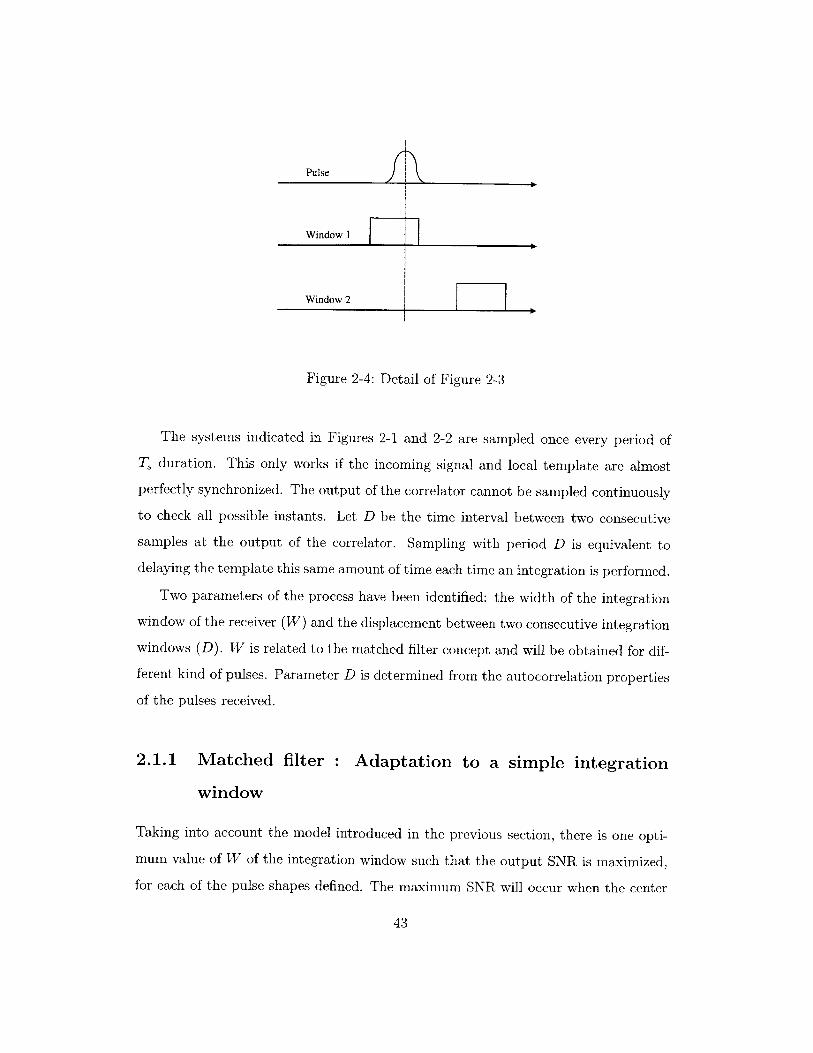
Pulse
Window 1
Window 2
Figure 2-4: Detail of Figure 2-3
The systems indicated in Figures 2-1 and 2-2 are sampled once every period of
T, duration. This only works if the incoming signal and local template are almost
perfectly synchronized. The output of the correlator cannot be sampled continuously
to check all possible instants. Let D be the time interval between two consecutive
samples at the output of the correlator. Sampling with period D is equivalent to
delaying the template this same amount of time each time an integration is performed.
Two parameters of the process have been identified: the width of the integration
window of the receiver (W) and the displacement between two consecutive integration
windows (D). W is related to the matched filter concept and will be obtained for dif-
ferent kind of pulses. Parameter D is determined from the autocorrelation properties
of the pulses received.
2.1.1 Matched filter Adaptation to a simple integration
window
Taking into account the model introduced in the previous section, there is one opti-
mum value of W of the integration window such that the output SNR is maximized,
for each of the pulse shapes defined. The maximum SNR will occur when the center
43

of the integration window is aligned with the center of the pulse. The output of the
integrator in the presence of AWGN is a gaussian random variable. The value of its
mean, for different pulses is:
" Rectangular pulse:
N,.W-Aif W<VI (W) =(2.6)
N V -A if W>V
" Triangular pulse:
N,-W-A if W < VI (W) = (2.7)
N, . W - A - Nc-A W2 if V < W
" Gaussian pulse:
I (W ) = N (- )- N ( )(2.8)V V
N, represents the number of pulses that are used to represent only 1 bit, and:
N (x) V e -2 dy (2.9)
Previous expressions represent the mean of a gaussian random variable after integra-
tion of the input signal with a window of width W. In order to completely characterize
this random variable, it is necessary to define its variance, which is related to the noise
spectral density. Assuming that the noise is white, its correlation function obeys the
equation:
R, (r) = o, 2 (T) (2.10)
Defining now:
p= J n (t) dt (2.11)
44

0.2 0.4 0.6 0.8 1W for V=1
1.2 1.4 1.6 1.8 2
Figure 2-5: Relation of SNRs in function of the relation between W and V
Then, the variance of p (and the variance of the integral) is:
Var (p, W) = o 2W (2.12)
The signal to noise ratio after the integral can be obtained by a ratio of amplitudes:
SNR (W)- (W)VVar(p,W)
(2.13)
In Figure 2-5 the variation of the SNR with the value of W normalized to the width
of the pulse V is depicted. From this plot, the optimum values of the width of the
integration window are obtained and shown in table 2.1.
2.1.2 Definition of Pd and Pfa
Each time a complete correlation of what could be the UWB representation of a bit is
obtained, its output is compared to a threshold in order to check if the UWB signal is
45
0.9
0.8
0.7
z 0.6C/)0
C 0.5000.20.4
0.3
0.2
0.1
1
0L0
.. . . ... ..
Rectangulapus- -Triangular u-s-- Gaussian pulse
-..-.. . - .- -- -G.ss.p.s

present. An issue to consider is that a sign reversal of the whole signal is possible due
to the absence of the direct path and the presence of echoes coming from reflectors.
To take this into account, the absolute value of the correlation is taken and its result
is compared to the threshold.
The probability of false alarm, Pfa, is related to the variance of the input noise.
Taking into account the input signal to noise ratio, we can model the result of using
its absolute value instead of only the value as seen in Figure 2-6. From this model:
Pfa = 2N (--) (2.14)
By the same method, the probability of detection (Pd) can be defined by considering
the relation of the threshold with the output mean and the relation of the output
mean with its standard deviation given by the signal to noise ratio. Then there are
two parameters of importance for determining both Pf a and Pd. Figure 2-7 shows
how the probability of detection changes as a function of the threshold. Figure 2-8
shows how the probability of detection, for the same SNR, decreases with Pfa.
2.1.3 Specification of the value of D
The output of the correlator is sampled with a period D. These samples will not
usually coincide with the center of the pulse. The SNR decreases when the integration
window and the pulse are not aligned, as the value of the signal integrated decreases,
while the variance due to the gaussian noise does not change. Figure 2-9 shows the
loss in SNR due to this misalignment for different kind of the pulses.
The value of D determines how many opportunities are available to detect the
Table 2.1: Optimum window ratio V/W.
Pulse W/VRectangular 1Triangular 1.4Gaussian 2
46

10Value of the integration
Figure 2-6: Pp, with absolute value.
10 0
110-1
110-2
CL 1 ()73
10 -4
110-5
10 -6
...... .........: ..........: ..........: ........................ .. ............................................................ ..... ...... ..... ........... ........... ........... ........... .I ......... ........
.. ... ..... ........... ...... ... .. ................... ......... ............ ..... ......... ..... .......... ..... ........... ........... ........... ........... ........... ...
...................... .... . ............ ......................
................. .... ........... ........... .......... . . . . . .. . .
....... .......... ...... .. ........... ........... ........... ........... ........... ............... ... ................... .... ..... .......... ............................W ...................
... ....... .......... ........................................................
.. ... ..... .......... .......... . ...... ...... .......................
I W
............ ...... ... ..... ..............................
.. ... ..... .......: ... ...... .... ...... ...... ...... ...... .. ......... ................................................... ... .............. ...............................
.. ... ..... ......... .......... .............................. .................. ...................
. ... .............. .........................
.......... ...... ........ ........... . ....... .
.. ... ..... ... ... .... ... . ...... . - 1 :- - ... *:* , -, * - * *: , '- , ': .. ... .... ... ..... .................. .. ........... ...............
.. ... ..... .......... ......................... ....................q .... ..... ...................
.. ......... ............ ....
............................. ..... ......... ...... ... ...... ......................... .......... ........... .. ........ ... ... ..... .......... ......... ...... ................................................ ..............
.. . . . . . . .. .. . . . . .. . . . .. . . . . . . . .. . . . . . . . . . .. . . . . . . .. . . . . . . . . .. . . . . . . . . . .. . . . . . . .7. .. . . . .. .. . . . . . : : : : M W.: : : : : : : : : : -, * * . . . . . . . .. . . . . : : : : : : : : : : : : : :-: : : : : : : : . : : : : : : : : : .. .. . . ... . . . . . . . . .. . . .... . . . . . . . .... . . . . . . . . .: : : : : : : : :
::: : : : : : : : : :: : : : : : : : : : : .. .. . . . . . . .. . . . . . . . .. . . . . . . . . . . .. . . . . . . .
. . .. . . . . .. . . . .. ... . . . . .. . . ... . . . . .. ... . . . . . . . . ... . . . . * ': . . * * * . . . . . . . . . .. .. . . . . . ..
. . .. . . . . ..I . . . . . . .. .. . . . . .. .. . .. . . . . . . . .. . . . . . . . . . . .. . . .
0 0.5 1 1.5 2 2.5Ratio T h /a
3 3.5 4 4.5 5
47
Threshold
/Pfa
-Threshold
Figure 2-7: Pfa with the threshold as parameter.

5 10 15SNR (dB)
Figure 2-8: Probability of detection with the ratio Th/- as parameter.
0 0.1 0.2 0.3 0.4 0.5 0.6Misalignment (fraction of W)
Loss in Signal to Noise Ratio due to misalignment of the integration
48
0.9
0.8
0.7
0.6
a.70.5
0.4
0.3
0.2
0.1
r)
fa =103- P i-
P =105fa
L ...... ....
...... .....
--.... --..-..---.-
0 20 25 30
- Rectangular pulseTriangular pulseGaussian pulse
- - -.. . ..... .....-. .-. -. -. -
q/
- - - - - - -- - - - - - - - - - -- -- -- --
- - - - --- -q
.........- -.. ........
25
20
15
10
5
Figure 2-9:window.
0.7 0.8 0.9 1
nn

WW
D
V Time
Figure 2-10: Situation of two consecutive windows for coarse acquisition considera-
tions.
same pulse. It is desirable to minimize the number of integration intervals in which
the pulse is present in order to minimize the clock frequency of the correlators. At
the same time, a minimum probability of detection must be ensured. Figure 2-10
shows the position of two consecutive windows with respect to a pulse centered at
the midpoint. Let r be the delay of the pulse with respect to the center of the first
integration window. The possible values of r are from 0 to D. The probability of
detection when the algorithm sweeps the possible delays from 0 to NNf V is the
probability of detecting the pulse in at least one of the two windows that include
it. Figure 2-11 shows the value of this probability as a function of D, averaged
for all possible values of r. Setting D equal to W gives a reasonable probability of
detection of around 0.90 for both triangular and gaussian pulses while the value for
the rectangular pulse falls below 0.9 as its energy is more concentrated. This and the
fact that this choice simplifies the timing design in the receiver as all clocks have the
same frequency, encourage the following relation D = W.
2.2 Definition of the coarse acquisition process as
a discrete stochastic process
This section defines an abstract model of the coarse acquisition process as a Markov
chain. Using the values obtained in section 2.1, the effect of the SNR and the shape of
49

G ussian pulse0.9 -C0
0.7 -CU
0*5
0.40.2 0.4 0.6 0.8 1 1.2 1.4 1.6 1.8
D (ns)
Figure 2-11: Pd in one of the two integration windows where part of the pulse ispresent as a function of D.
the pulse on the expected time to synchronization (E [k]), the probability of correct
detection (Pa) and the probability of false detection (Pfd) are examined. Afterwards,
a way of summarizing this process when several tests can be performed at the same
time, using parallel architectures, is introduced. A similar analysis appears in [9], but
the probability of false alarm in the decision and the order at which the correlations
are obtained are completely ignored. Here, both factors are taken into account.
Precisely the duty cycle of the signal prevents the receiver to use methods common
in CDMA receivers like using a template with a clock at a slightly faster frequency
[8]. In the case of an UWB signal, the possible increase of frequency is small if a fair
amount of the processing gain is still needed during this process.
2.2.1 Coarse acquisition as a Markov chain
The initial assumption is that the position of the pulse with respect to the integration
window, r, does not change from one pulse to the next inside a bit. This is reasonable
if the transmitter and receiver clocks have exactly the same frequency and there is
no jitter in either of them. The expressions will be deduced assuming a fixed value
for r. To take into account all the possible values of r, Bayes theorem is used.
The model of the coarse acquisition process can be seen in Figure 2-12. In each of
the states depicted (except for FD and D) a template with that delay is correlated to
50

D
S2 ------- i-1 ii+ 1 ----....------
FD
Figure 2-12: Coarse acquisition as a Markov process.
the received signal. The initial state can be any from state 1 to state N = NcN. The
states i and i + 1 contain the pulses almost properly aligned. If the pulse is detected
there, it goes to state D, correct detection (with probabilities P,i and Pd,si+) The
rest of the states do not contain the pulses. Any detection in those states implies a
false detection (state FD) with probability Pfa. If no signal is detected, from each
state the process can only jump to the next one.
The transition probabilities of this process are:
" States 1, 2, 3, ... ,i -1,i + 2,..., N-i.
- Pf, ifj=k+1
Pk,j Pfa if j = FD (2.15)
0 otherwise
* State N.
( - Pfa if j = 1
PkJ Pfa if j = FD (2.16)
0 otherwise
51

. States i.
e States i + 1.
I - Pd,i
PJ P,i
0
I - Pd,i+1
PiJ= Pdi
0
if j - i + 1
ifj - D
otherwise
if j i + 1
ifj - D
otherwise
Using the nomenclature of [61, this model has three classes: one of them is transient
of period N and the other two are recurrent, aperiodic and consisting respectively in
states D and FD.
2.2.2 Mathematical characterization of the model for coarse
acquisition
This section outlines a procedure to obtain, from the probabilities of detection and
probabilities of false alarm obtained in section 2.1, the following parameters:
e Expected time of acquisition.
* Probability of correct detection (Pcd).
e Probability of false detection (Pfd).
Let k be a discrete random variable that represents the number of integration windows
examined before declaring a detection. If the probabilities of declaring a detection
for the slots jfrom I to N is Pj, then:
Pd, i
pi = Pd,i+1
Pf a
if j i
if j = i + 1
otherwise
(2.19)
52
(2.17)
(2.18)
Since any integer number k can be expressed as follows:
k = n + m - N (2.20)
Then, the probability mass function of k is:
n-1
Pr [k] =Pr [n + m - N] = Pr [n] A" = PnA"'Pn (1 - Pj) A m (2.21)j=1
whereN
A = rl(1 - P) (2.22)j=1
and:n-1
Pr [n] = Pn H(1- Pj) (2.23)j= 1
Two useful relationships are obtained: The first one is the probability of having a
detection in the slot n with n = 1, ... , N, that is, the probability of making a detection
in any of the slots n, n + N, n + 2N, ..., n + m - N, ... for any m integer. Let that
probability be denoted as Pr [h]. Its value is:
Pr [h] = (2.24)
The second useful relationship is:
N
EPr [n] 1 - A (2.25)n=1
Using this information, the parameters that characterize the process are the expected
time of acquisition E [k], the probability of correct detection Pcd and the probability
of false detection Pfd:
E [k] n=1 (2.26)
(Pi + Pi+1 (1 - P)) H-- (1 - P)(Ped = (2.27)
53

Pfd = 1 - Ped (2.28)
These results have been obtained for the pulse occupying the bin i and for a concrete
position s of the pulse with respect to the integration window. Then the previous val-
ues can be denoted as functions E [k, , S1 sNR, Pd (i, s, SNR) and Pfd (i, s, SNR).
The useful parameters are obtained by averaging these functions over i and s:
N DE [k, SNR] N D E E [k, i, d, SNR] ds (2.29)
N D
Pead(SNR) = N D Z j Pcd (i, s, SNR) ds (2.30)
PfdN(SNR) =N D Pfd (isSNR) ds (2.31)
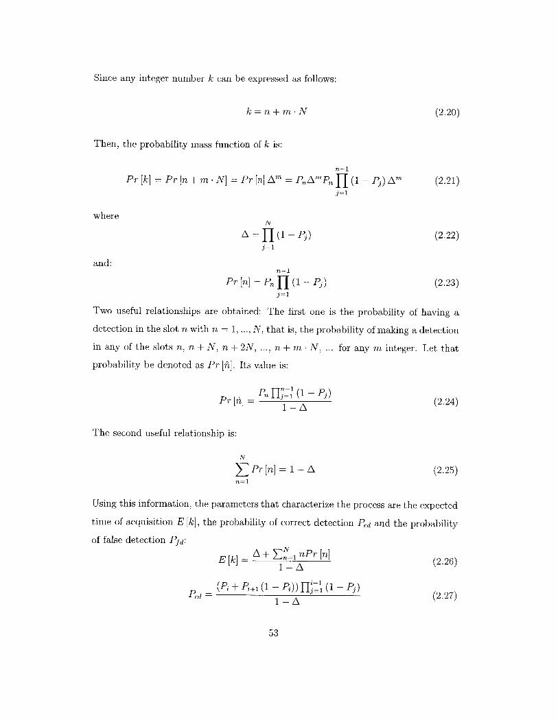
Using these equations, and choosing N, = 31 and Nf = 50, table 2.2 is obtained. The
average of k is given as the number of decisions or states examined. It is observed that
the probability of correct detection drops sharply when Pf, = 10-3. This happens
because Pf a is comparable to 1/N, and in N trials, more than one false alarm will
usually arise. Then, in order to ensure a reasonable probability of correct detection,
Pfa must be lower than 1/N. It is observed in this table that the probability of
correct detection increases as the probability of false alarm decreases. Traditionally,
the probability of detection decreases as the probability of false alarm decreases as
it was already seen in Figure 2-8. The reason of the behavior observed in table 2.2
is that the probability of correct detection is not a probability of detection in only
one decision: it takes into account that no detection is declared in the wrong time
slots. As it is, if the probability of false alarm is high, the probability of declaring a
detection in a slot with no signal before a trial in the right slot occurs increases, and,
as a result, the probability of correct detection decreases.
54

Table 2.2: Model results
Rect. Triang. Gauss.
Pfa E[k] Pcd E[k] Pd E[k] Pcd10-3 1930 0.42 1988 0.47 2016 0.4810-4 903 0.87 927 0.90 942 0.9110-5 801 0.98 809 0.99 821 0.99
2.2.3 Generalization of results when parallel architectures
are possible
All the previous analysis is characterized by
following sequence of operations.
the fact that the receiver performs the
1. Set n = 1.
2. Perform correlation with input signal assuming the delay of the incoming pulse
is equal to n.
3. Compare the value of the correlation with a threshold.
4. If the threshold is exceeded, declare coarse acquisition lock and end.
5. n=n+1.
6. If n = N + 1, then n = 1.
7. Go back to step 2.
With this procedure the system advances from one state of the Markov chain to the
next one. The different possible delays are tested sequentially, and only one possible
delay is checked per iteration. Reference [9] suggests that the mean time to declare
coarse acquisition lock can be reduced by checking the possible delays in a non-
sequential order by maximizing the average distance between two consecutive delay
checks. This procedure ignores the time between two consecutive correlation values
are obtained. This time is equal to the distance between the two delays that are being
tested. By maximizing this distance, the time between checks is also maximized, so
55
the fact that the average number of checks is reduced by half is overcome by the fact
that the time between checks is increased by the distance between two consecutive
delays checked.
A simple way of reducing the number of decisions is to run several different cor-
relations in parallel [5]. In this way, several delays are checked at the same time. If
Nf delays are checked concurrently, the average number of iterations needed to check
all the delays is divided by Nf. The average number of iterations to detection can
be obtained by dividing the average number of iterations in table 2.2 by Nf. The
best that can be done would be to perform the N checks in parallel, but the number
of operations needed and the memory necessary to store the results are large, which
makes its implementation difficult.
2.3 Effect of a difference in frequency between clocks
A difference in frequency between the transmitter and receiver clocks affects the
synchronization process. A model to include this effect is introduced in this section.
The performance of the coarse acquisition algorithm is tested under these conditions.
2.3.1 Conventions and models
Both for the rest of this chapter and for the next in which fine tracking is studied, a
model that includes timing imperfections is needed. Among these imperfections are
the difference in frequencies between the transmitter and receiver clocks and jitter in
any part of the transmitter or receiver chains.
If the transmitter and receiver clocks have the same frequency, the position of the
integration windows with respect to the pulses does not change between pulses. If
there is a difference in frequencies, the pulses do not change, but the relative position
of the pulse with respect to the integration window changes among the pulses that
comprise one bit and also between bits.
The difference in frequencies is usually expressed in parts per million of the ex-
56

r[njj]
Cetr of the pulse
Figure 2-13: Notation on the pulse position estimation
pected frequency. Let this difference be stated as:
k = (2.32)fo
where f, is the frequency of the receiver clock that is chosen to be our timing reference
in our description of the system. Then, the frequency of the transmitter is f0 (1 + k)
and the difference of frequencies k is expressed as a fraction of 1. If k is not equal to
0, the position of the pulse relative to the integration window moves from one pulse
to the next. The change in this timing position is:
Nf Nf Nf k Nf k (2.33)fo (1 + k) fo fo 1+k fo
The last approximation is correct as k << 1.
Each received pulse is straddled between two integration window as seen in Figure
2-10. In the following, sub-index 1 refers to those expressions related to the first
integration window, while sub-index 2 refers to the expressions related to the second
integration window. Let r be redefined as the position of the center of the pulses
with respect to the division between the two integration windows. r changes not only
with each bit but also between pulses that are intended to compose a bit. Let r [n, i]
be the delay associated to the i pulse in the representation of the bit n. n can have
57

values from -oo to oc, while:
Nc - 1 Nc - I
2 , ... , -1,0, ' 2(2.34)
An individual pulse produces two values of the integral in the two windows:
(2.35)
(2.36)
The total integral value at the output of the correlator is obtained by summing over
all the pulses that comprise one bit:
N-12
2
2
I1 [n, i] (2.37)
(2.38)12[Tn]V 1=- Nc-1
2
It is possible to relate every r [n, i] to the value for the center pulse r [n, 0]:
r [In,i] = r [In, 0] + iAT (2.39)
Then, rewriting (2.35) and (2.36) as
(2.40)
(2.41)
Taking into account the symmetry of 1 [n, i] and 12 [n, i] with respect to the central
pulse:
(2.42)
(2.43)
58
11 [n, Zi] = A (I - r [n, fl)
I2 [n, Zi] = A ( T + r [n, fl)
12 [n , Zi
I1 [n, i] =A (T - r [n, 0] - iA T)
I2 [n, Z] =A (T + r [n, i*] + i*dT)
I, [n] = NcA (I - r [n, 0])
I2 [n] = NcA (T + r [n, 0])

It is not necessary to specify that the delay included in these integrals is that of the
central pulse. It is possible then to drop the zero and these equations become:
I1 [n] = NcA (! - r [n]) (2.44)
12 [n] = NcA (I + r [n]) (2.45)
2.3.2 Non-idealities of the estimator
In the previous analysis it has been implicit that the integration windows were as long
as needed and only the position of the center of the pulse compared to where one
integral finished and the other started was important. In this design, both for reasons
of processing gain and speed in determining the delay, an integration interval that is
equal to the width of the pulse has been chosen. If the frequency of the transmitter
and that of the receiver are not equal, each individual pulse will not have the same
position compared to this integration limit. Furthermore, it is possible that a pulse
moves enough to shift completely out of one of the integration intervals. Equations
obtained in the previous subsection must be corrected to include this possibility.
Let r [n] > 0 and k < 0. Therefore, AT > 0 and the difference between the center
of the pulse and the time reference grows monotonically with each pulse. If the width
of the pulse is V, the maximum AT allowed is:
V N -iV-- r [n] + = AT- . - (2.46)2 2
If AT is greater than this value, then part of the pulse that should be integrated in
the second interval is lost for another interval. Reordering this equation and taking
into account (2.33):
k 2f o (r[n A(r[]) (2.47)1 + k Nf (Nc 1) [ 2 =
From this,A (r [n])
1 -A (r [n]) <k < 0 (2.48)
59

This value provides a first bound. Under this condition of k the equations in the
previous section hold. As1
0 < r [n] < (2.49)-- 2fo
If not, then part of the value of the integral goes to another interval, and the SNR
decreases. For these values, it can be shown that:
1 f r [n] - < 0 (2.50)2 2
and1
- < A (r [n]) < 0 (2.51)Nf (Nc - 1)
Figure 2-14 shows the absolute value of this upper bound. In the worst of cases a
clock with a stability of 20 ppm allows Ir[n] I < 0.970 ns while a clock with stability
50 ppm allows Ir[n]I < 0.925 ns. On the other hand, if the delay is outside these
values it does not mean that the system will not be able to detect and lock onto the
signal. It only means that there is loss in SNR.
If the frequency deviation exceeds the bounds indicated by Figure 2-14, the value
of the integration is no longer the maximum and the signal is no longer confined to
only two integration windows but to three. In order to properly analyze this situation,
it is necessary to obtain the number of pulses that are completely included in the two
intervals of integration. This number is given by:
V - (r [n] + V)mi= AT (2.52)
Also we define:
Nc2 - 1 (2.53)2
For each of the pulses integrated, their contribution to the first integration window
is:
I, [n, 0 = A - - r [n] (2.54)
60

0 0.1 0.2 0.3 0.4 0.5r in ns
0.6 0.7 0.8 0.9 1
Figure 2-14: Maximum frequency deviation for starting to have SNR loss as a functionof position r.
I, [n, 1] = A - (r [n] + 1 -AT) (2.55)
I, [n, -1] = A - (r [n] - 1 -AT) (2.56)
(r [n] + mi - AT) )
11 [n, -ml] =A -( - (r [n]
I, [n, j] - 0
V1 [n, j] - A - (r [n]
The sum of all these integrals is:
1 [n] =NA -(2.61)
+ AATNc2 + Mi + 1
2
61
700
600
c,500
0
C
300
E
200
100 F
- .... ... ........... .
- - - - .. -... ...- .. .......... . .
- ~~ ~ - - .. ....
.-- -- - -- - - - -- - -. -.- .......... .
- - - -........ -......
- - - - -- -- - - ..... ..... -
-. - - - - - .- -.
I, [n, m1 ] = A - -
-mi .AT))
J -AT) )
(2.57)
(2.58)
(2.59)
(2.60)
- (Nc2 - n 1 )
-r [n]) - A -V- r [n] )- (Ne2 -- ml)

The contribution of each of the pulses to the second integration window is:
12 [n, 0]
I2 [n, 1]
I2 [n, -1]
I2 [n, mi]
12 [n, -mi1 ]
'2 [nj]
2 [n,-j]
+ (r [n] + mi
+ (r [n] - j .
The second integration has the value:
I2 [n] = Ne A 2 + r [n]
- 2AAT Nc2 + m
2
V+ 2A (2- r [n] -(Ne2 - Tn1)
-+. (Nc2 - M1)
Finally, a part of the energy of the pulse spills into another integration window.
13 [n, 0] = 0
13 [n, 1] = 0
13 [n, -1] = 0
13 [n, mi] = 0
13 [n, -mi] = 0
13 [nj]
13 [n, -j]
+ J -AT)) (2.75)
(2.76)
=A- +(r[n]
=0
62
AT))
.AT) )
(2.62)
(2.63)
(2.64)
(2.65)
(2.66)
(2.67)
(2.68)
- m, - AT) )
.AT))
AT))
(2.69)
2.70)
2.71)
2.72)
2.73)
.74)
=A V + (r [n] + I -
=A V
=A (V- (r [n] + j
=A V
=A V+ r [n]
=AV+ (,r[n] -I1- AT))
=A (V+ (r [n]

The value of the third integration is:
I3 [n] = -A 2 -r [n] (N 2 -mi) (2.77)
+ AAT +(Nc2 - M1)2
The signal is present in three integration windows. There are now three opportunities
to lock onto the signal instead of two. In addition, if part of the energy spills to other
integration windows, we can expect the probability of detection in each of them to be
smaller than before. The new probability of detection has the following expression:
Pd 1 - (1 - Pdl)(1 - Pd2)(1 - Pd3) (2.78)
were the Pdl is the probability of detection associated to 11, P2 is the probability
of detection associated to 12 and Pd3 is the probability of detection associated to
13. Figure 2-15 shows how the probability of detection decreases as the frequency
difference increases. This figure shows various curves, each one for a different value of
the position of the center pulse in the series that represent a bit. The delays used for
this plot are such that for reasonable clocks stability (below 100 ppm) some problems
can be expected. It is seen in this figure that for these values of stability the loss
in probability of detection is negligible. A quartz clock will provide only 20 ppm.
Better specifications are possible but at a larger cost that makes them not suitable
for most commercial applications. The coarse acquisition process does not change its
properties because of a difference in frequency. All analysis performed in the previous
sections are valid, with the caveat that the fine tracking algorithm must also work for
the same range of frequency differencies.
2.4 Summary
In this chapter the coarse synchronization process for an UWB system has been
analyzed. The quest for simplicity has led to the use of an integration window instead
63

0.99 r=05.
r=0.49
0'0 0.985 - - ----- -- - --0.7 r=0.47
0.9 7- - -- -0-
0 .9 7 5 - - ... r=0 .4 4 ... . .. . . ... .. .. .. .. .. .. ... .. .. .. .. .. ..
r=O 4.1
0 10 20 30 40 50 60 70 80 90 100k in ppm
Figure 2-15: Change of probability of detection due to a difference in frequenciesbetween transmitter and receiver
of a perfect replica of the pulse. The system of using non-overlapping windows to
detect a peak of correlation works with reasonable probability of error for triangular
and gaussian pulses, while for rectangular pulses it would be necessary to overlap the
integration windows. The analysis takes into account the impact of false alarms in
the process, revealing that the probability of false alarm must be below 1/ (NcNf) to
ensure a reasonable value of Pd and E[k]. The impact of a difference in frequency
between the transmitter and receiver clocks is incorporated into the analysis and it
is revealed that for the values usually encountered in quartz oscillators, the loss in
probability of detection (and, therefore, the loss in performance) is negligible. Jitter
does not affect the coarse acquisition process and its impact in fine tracking process
is analyzed in chapter 3.
64

Chapter 3
Fine Tracking
A fine tracking algorithm ensures almost theoretical performance of the receiver even
when there is a difference in frequency between the transmitter and receiver clocks,
jitter due to the different elements in the transceiver chain or Doppler effects due to
relative movement of the transmitter respect to the receiver. It allows the transceiver
to use longer data packets for the communication since it can maintain lock of the
signal for a much longer time.
However, a fine tracking algorithm is not always necessary. The coarse acquisition
algorithm has been designed to make an initial rough estimation of the incoming
delay of the signal and, under certain conditions, this estimation could be enough for
the whole data packet. In this chapter, these conditions will be taken into account.
After that, the analysis and implementation of the fine tracking algorithm comprised
of a classical DLL taking into account non-idealities will be included.
3.1 Necessity of a fine tracking algorithm
It has been mentioned that if the data packet is short enough there is not a real
necessity of implementing a fine tracking algorithm as the timing will be good enough
for the detection of the rest of the packet once coarse acquisition has finished. In this
section the nature of the bound on the length of the data packet is given.
The errors that a fine tracking algorithm corrects are differences in frequency be-
65

tween transmitter and receiver and jitter. A difference in frequency implies that the
position of the center of the pulses is steadily changing with respect to the integration
windows chosen to detect the signal. The presence of jitter implies that each individ-
ual pulse has a random position around what should be the center of the pulse. Due
to the model used here, the mean error added by the jitter is zero. Then, to estimate
the maximum length of the data packet, only the possible difference in frequencies is
taken into account.
In chapter two, it was shown that if the difference in frequencies was expressed
as:
k = (3.1)fo
then the relative change of position between two consecutive pulses is:
A T 1 k (3.2)f, I + k
Let us assume that, after the coarse acquisition algorithm, the center of the first
received pulse is situated exactly between the two integration windows (r[n] in figure
2-13). If there is a frequency difference between transmitter and receiver, then this
center of the pulse moves with respect to the boundary between the two integration
windows. If the center of the pulses moves in any direction V/2 then one of the
two integration windows does not contain the pulse anymore and SNR lowers. The
number of pulses necessary for this to happen is:
niPulses = K2A TI_ 2Nfk _ (3.3)
For the specifications of the system, if k = 20 ppm, nipuses = 250. If each bit is
represented by N, = 31 pulses, this allows a maximum of 8 bits in the packet. If each
pulse represents a bit, it allows 250 bits. In order to receive longer data packets, a
fine tracking algorithm is needed.
66

r~~n] e~[n] , 1cn
g~n]A(z)
Figure 3-1: Fine tracking block diagram
3.2 Analysis
In this section, a behavioral model of the system after coarse acquisition is introduced.
This model will not take into account all the hardware elements of the system but it
will allow the analysis of all the timing imperfections.
3.2.1 Model of the system after coarse synchronization
The block diagram representing the fine synchronization system is depicted in Figure
3-1. The loop is implemented with the filter F (z) and the integrator A (z).
The input of the tracking loop is the signal r [n]. It is analogous to the input
phase in a Phase Locked Loop (PLL) and represents the n-th estimation of the delay
of the center of the bit with respect to where it should be. n is associated to the
number of bits after coarse acquisition that have been used for fine tracking. g [n] is
the output of the loop that is intended to follow r [n]. The difference between these
two values is represented by the error signal e [n].
A bit is encoded as a sequence of N, pulses, using a frame of Nf. r [n] can be
referenced to any instant between the beginning of the bit to the end of the bit.
Without loss of generality, this reference position is chosen to be the center of the bit
as indicated in Figure 3-2.
It is possible to obtain a model of the input signal that incorporates all the timing
errors that the system needs to track. If only the increment in time from the center
67

e[n] -Expected position of the Center of the central pulse r[n].center of the central pulse gin].
Nf pulses = I bit
Figure 3-2: Timing references for the Delay Locked Loop
of one bit to the center of the next bit is considered, then r [n] obeys to the following
expression:
r [n + 1=r [n] + NNfT + s [n] (3.4)
In this model, the loop is completely digital. This implies that the signal at the
output of the block equivalent to the VCO (the integrator A (z)) is perfect. It adds
no jitter and is not a source of noise. All the timing noise can be considered to be at
the input. The trade off that sets the design of the loop filter in this case relates the
pull-in and pull-out ranges of the DLL with noise injected along with the signal [12].
s [n], from equation (3.4), models all the elements in which the timing of the
incoming signal deviates from what is expected of it (that is, that the duration of all
bits is the same and equal to the one generated at the receiver). In the same way,
g [n] can be written as:
g [n+1] = g [n] + NcNT + c [n] (3.5)
where c [n] is the update obtained from the loop for next iteration. The term NcN 1 T
is additive and common to both expressions. The signal in the loop is:
e [n] = r [n] - g [n] (3.6)
68

s~n]g[n] ACz)
Figure 3-3: Fine tracking block diagram, interpretation
this common term can be ignored. Then:
r[n+i] = r[n]+s[n] (3.7)
g[n+1] = g[n]+c[n] (3.8)
These are the equations of a classical DLL. The block diagram from Figure 3-1 can
be redrawn taking this last two equations into account. The result is given in Figure
3-3. From equations (3.7) and (3.8), the value of the block A (z) is:
1A (z) = 1 (3.9)
z _ 1
The expression that relates the input signal s [n] with the error can be obtained:
E (z) _ 1H (z) S(z) - (3.10)S (z) I + F (z) A (z)
Replacing equation (3.9):
H (z) =1(3.11)F (z) z--1 + 1-z-1
It is interesting to rewrite these equations combining the two filters present in the
loop F (z) and A (z) as
G (z) = F (z) A (z) = F (z) z-1 (3.12)1 - z-1
69

In this situation, the error transfer function can be rewritten as:
E(z) A (z) S (z) z_1S (z)E (z)) =(-z)(±Gz= (3.13)1 + G (z) (I - z-1) (I + G (z))
The filter F (z) is specified by the fact that it must be able to correct:
" An unknown difference in delay.
" An unknown difference in frequencies between the clock in the transmitter (that
determines the width of the pulses and the separation between two consecutive
pulses) and the clock in the receiver (that determines the sampling rate).
" Input noise coming from two sources: white noise that adds to any signal re-
ceived, and jitter, both coming from the transmitter and added at the receiver.
Models of these imperfections will be included along the chapter.
The possible choices for F (z) (or, as preferred, G (z)) are many. Let:
PF(z)G (z) = 2Z (3.14)(1 - z-1)2
where P (z) is a polynomial in z- 1 (not a fraction). The necessity of this kind of
transfer function will become clear in the next sections.
3.2.2 Effect of a frequency offset
A frequency difference between the transmitter clock and the receiver clock is pro-
duced when the input of the system s [n] is equal to the following expression:
s [n] = A - u [n] (3.15)
where u [n] is the step function. Its z-transform is:
kS (Z) = ROC = {z E C such that |zi > 1} (3.16)
1 -
70

The z-transform of the output error of the loop is
Z-_ A
E (z) - 1-Z 1
( P(z )1± _Z-1)2
(3.17)
Optimally, the response to a step should be a decreasing exponential of the form:
e [n] = k'a"nu [n - i] (3.18)
In order to obtain that, the denominator of its z-transform must have the form 1 -
az- 1. It works if:
P (z) = (1 + b) z- 1 - Z-2 (3.19)
ThenAz- 1
aEz - (I-b) z-1
Therefore, the step response is
e[n] k (1 -b)n-u [n- 1]
(3.20)
(3.21)
It will be a decaying exponential if
11 - bI < 1 (3.22)
3.2.3 Effect of a delay difference
Taking into account the model, a phase difference is produced when the input of the
system s [n] is equal to the following expression:
(3.23)
It can also be expressed as:
s [n] = A (7j [n] - ? [n - 1])
71
(3.24)
s [n] = A - 6 [n]

From the step response previously obtained,
e [n] = A6 [n - 1] - Ab(1 - b)n-2u [n - 2] (3.25)
If the step response is a decaying exponential, so is the impulse response. In both
cases the error stabilizes to a null value.
3.2.4 Effect of random noise
It is assumed that the noise that accompanies the estimation of the delay of the signal
is gaussian and white. In this model all the noise is injected as an additive component
for r [n]. If the noise spectrum at the input is white, its spectrum at the output of
the loop, taking into account the transfer function from the input r [n] to the error
e [n] [16]:
1 (1 -z-1) 2H (z) =-,)2 (3.26)1 + G (z) I + (b - 1) z-1
The power spectrum at the error output of the loop is then
San (z) = H (z) H (z 1 ) (3.27)
Or, particularized at the unit cycle, in function of the frequency:
San (eiw) = IH (ej) 12 (3.28)
Figure 3-4 shows the shape of several filters in function of the value of the param-
eter b. The filter is always a high pass filter in which the bandwidth is related to the
value of b. As the value of b increases and approaches 2, the bandwidth decreases and
the filter approaches a delta at high frequencies.
3.2.5 Choice of the coefficients of the filter
The filter is fixed by choosing a value of b. There is a trade off between the speed to
eliminate a difference in frequencies and to minimize the noise bandwidth of the loop,
72

0 .9- - - - -- - .------ -
0.8-
0.7-
0.6 - - - -----
0.5 --b=0.05
0.4 - - - - - ---0.5
b=0.3-
b=10.2-
b=1.60.1
1 -0.8 -0.6 -0.4 -0.2 0 0.2 0.4 0.6 0.8 1Normalized frequency
Figure 3-4: Spectrum of error noise depending on the value of b
so that any noise at the input is minimized. In order to design the step response to
decay rapidly, b must be as close to 1 as possible, so that lb - 1 is small. On the
other hand, if the noise bandwidth is to be as small as possible, b should be close to
1. A good choice will depend on the noise environment.
3.3 Definition of the delay estimator
In the previous analysis, it was assumed that the difference between the input delay
and the delay generated in the local system (represented by the error e [n]) is exactly
known. This is not true since e [n] is estimated using the result of the correlation of
the input signal with the local version of it.
The local version of the signal is a low-order approximation of the incoming signal.
It integrates the incoming signal, providing a sub-optimal approximation to the clas-
sical matched filter approach. From the point of view of the quality of the estimation
of the delay of the signal, it is necessary to compare the center of the received bit
with the expected position.
The data that is available to perform the estimation is just the output of the
73

correlators for the two integration windows chosen as the two containing parts of the
signal. From the previous chapter, the value of these integrals is:
/V\11 [n] =NcA ( - r [n] (3.29)
I2 [n] =NcA - + r [n] (3.30)
A possible estimator of the delay (r [n]) is:
[n] = - - [n] (3.31)2 12 [n] + 11 [n]
This estimator has several problems:
* Both 1 and 12 are gaussian random variables, not deterministic quantities. The
estimation is noisy.
* Equations (3.29) and (3.30) assume that the frequencies of the transmitter and
receiver clocks are exactly equal. This is not completely true and the impact
of the difference in frequencies in the estimator of the delay must also be taken
into account.
" It is not a good idea to implement a circuit performing a real time division at the
frequency this circuit should operate. This will be replaced by a multiplication
by the inverse. It will add some quantification noise.
* The corrections are digital. In fact, the possible corrections that can be done in
this system are not continuous and are bounded, and are an architectural issue
that will be treated in the next chapter concerning implementation.
These problems are treated in the following sections.
3.3.1 Impact of AWGN
Due to the AWGN at the input of the receiver, I1 [n] and 12 [n] are gaussian stochas-
tic processes. It is necessary to check if the noise present in the estimator can be
74

approximated as gaussian noise. If it is true, then the linear analysis performed in
the previous sections is correct. Let us redefine these integrals as:
(V\-1 [n] =ANc - r [n] + 61 [n] (3.32)
12 [n] =AN ( + r [n] + E2 [n] (3.33)
where the first part of both expressions is deterministic and 6i [n] and E2 [n] are discrete
stochastic processes. 61 [n] and 62 [n] can be modeled as independent white gaussian
random process with zero mean and the same variance.
The problem of the estimator used here is that the noise appears in the denomina-
tor, thus invalidating the assumption that the noise at the input of the fine tracking
loop is gaussian:
- V . 12 [n] + C2 [n] - h1 [n] - e1 [n] (3.34)2 12 [n]+ C2 [n] + I, [n] + ci [n]
However, if ci [n] and 62 [n] are small compared to I, [n] and I2 [n], then it is
possible to use a Taylor series expansion wit high confidence in accuracy. This is a
safe assumption since the signal to noise ratio after correlation is greater than 10 dB.
Therefore:
V I 2 [n]+ 62 [n] - Ii n] - E, [n]
2 12 [n] + I, [n] (3.35)V I2 [n] + 62 [n] -I, [n]--i [n
2 (12 [n] + I [n])2
Reordering the terms:
V V 2 [n]+ 62 [n] - I, [n] - c [n] _E2 [n] + el [n]2 12 [n] + I, [n] [n] + 11 [n])
Since 162 [n] + Ej [n]l << 1I2 [n] + 11 [n]1:
V[n] ~ - 12 [n] + 62 [n] - I, [n] - [n] (3.37)2 12 [n] + I1 [n]
Therefore, the assumption that the estimator of the delay is affected by additive
75

gaussian white noise is correct.
3.3.2 Impact of difference of frequencies
As it was seen in the previous chapter, equations (3.29) and (3.30) can be changed
to model the difference in frequencies:
VVI1 [n] =Ne A - - r [n]) - A -r [n] -(Nc2 - m1)
(3.38)Nc2 + in1 + 1
+ AAT C (Nc2 - mi)
VVI2 [n] =NeA -+ r [n] + 2A -V - r [n])- (Nc2 - m1)
(2 2 (3.39)Nc2 + mi1 + I- 2 AAT 2 .(Nc2 - mi)
2
where Nc2, mi and AT were defined in equations (2.53), (2.52) and (2.33). Integration
13 from equation (2.77) is not taken into account in this analysis since the receiver
is estimating the delay based on only two integrations. Figure 3-5 shows how the
estimation of the delay changes for differences between the transmitter and receiver
frequencies of 20 ppm, 50 ppm and 100 ppm. Since the differences are so small, a
detail view of Figure 3-5 is shown in Figure 3-6. The conclusion is that the frequency
differences usually encountered due to difference of clocks do not affect the receiver.
3.3.3 Impact of the granularity of the division
To perform a division consumes time and power. It is avoided as much as possible.
A way around the division is to store inverses of the possible numbers in a ROM and
access them as needed. Using the result of the addition I1 + 12 as addresses to the
ROM, a coefficient is obtained from it and used to multiply to the result of I2 - I.
Let examine more closely the change in the operation. An exact division by x can be
equally obtained by multiplying the number of the numerator by 1/x.
First, x is quantified using only the more significant ni bits to represent it. These
ni bits are the address of a position inside a ROM that contains an approximation
76

0.5
0.45
0.4
0.35
0.3
0.25
8 0.2
0.15
0.1
0.05
00
Figure 3-5: Estimaand receiver
0.05
tion of
0.1
the
....................... ............. ..... ......... ...... ......
-.........-. ..............-. .....-- -. ..- -.- -. .-- -- -- --.- -.- -. .- -.
- -- - - - - - - - - - -
- .............. -.. . -.. .... - -. ... ....
--... --.
- - - - - - - -- - - - - - - -- -- - - --
-p
- ...-. .-. .-. .-. -
0.15 0.2 0.25 0.3 0.35 0.4 0.45 0.5r[n]
delay with a frequency difference between transmitter
0.49
0.48
0.47
E0.46
0.45
0.44
0.43 0.44 0.45
Figure 3-6:
ppm
20pp
k=50 ppm
k 100 ppm- --- - - -- --
- - - -- - - - - - - --
- ----- - - --- --- - -- --- - - - - - - - -- - - - - --- --
0.46 0.47 0.48r[n]
Detail of Figure 3-5
77
0.49 0.5

to the coefficient that should be multiplied, that works for all the margin of values.
The number chosen to replace the coefficients must be such that it minimizes the
mean square error for that interval.
Error = c) 2 dx (3.40)
This error is minimized when:CInb - ina (3.41)
b - a
The previous equation yields proper results only when none of the limits a or b
are 0. The ROM has a finite number of positions, so only a finite number of intervals
can be represented using this technique. Therefore, there is a maximum number and
a minimum number that can be represented. This will set the dynamic range of our
receiver.
A measure of quality of the system is given by the mean square error for all the
values represented. In order to calculate that for each number of bits, it is considered
that when c is used to represent the interval from a to b, the square error for that
interval is:
Error (1- - - (ln b-lna) (3.42)(a b b - a
The mean square error is obtained by adding the error for all the intervals and dividing
between the number of intervals. It is shown in Figure 3-7 that for a number of bits
smaller than 5, a large error is obtained while, using a number of bits greater does not
decrease this error by much. As an adequate trade-off between precision and size of
the memory necessary to represents these values, it is chosen that only the five most
significant bits of the number will be used. The error will certainly increase when the
signal is small, but an automatic gain control helps to avoid small signal amplitudes.
78

0.04
0 .0 3 8 ..-- - -.-.-- ---- -.-.-.-.-.---.-. -.-- -.-.
0 .0 3 6 - - - - -- - - - - -- --.-.
0 .0 3 4 - - --- -- - - - - - - - - - - -- - - --....
0.032-
0 .0 3 - - - - - - -- -.-- -.-- -.- -.-. .- -. ..
0 .02 8 - - - - -- -- -- - - - - - - - --.
0 .0 2 6 - - --- --- -- --- -.-- - -. .-- -.-.- -.-.-.-.-. .
0.024-
0.0222 3 4 5 Nubrf s 8 9 10 11Number of bits
Figure 3-7: Mean square error due to quantization as a function of the number of bits
3.3.4 Granularity of the corrections
Due to the architecture used, only a limited range of delay corrections can be applied.
Although this can be increased by buffering, a non-buffering architecture will be
presented in the next chapter that allows for corrections of -3, -2, -1, 0, 1, 2 and 3
samples. That corresponds to delays of -1500 ps to +1500 ps, taking into account
that the sampling frequency is 2 GHz.
The impact of this will be studied only in the global simulation performed in the
next section.
3.4 Specification of the total jitter of the system
The total jitter of the system has been dumped at the input of the fine tracking loop.
The jitter will cause an error to appear at the output of the tracking loop. Two
different kinds of errors can be considered:
* The fine track system provokes an instantaneous error that needs a correction
of the delay greater than the three samples this system is able to correct.
79

* The jitter provokes a total timing error that makes the pulse get out of the two
integration windows that are used for estimating the fine tracking correction.
The total jitter at the receiver is the sum of the jitter caused by both the receiver
and the transmitter. Let each of the jitters be modeled as an additive white gaussian
noise with zero mean and standard deviation ajitter. The jitter from the transmitter
and the jitter from the receiver are independent stochastic processes. When they are
added together, the total jitter present in the system is a gaussian process of zero
mean and variance:
2 2 2atotal =Ujitter + Ojitter =2o, - (3.43)
Since the jitter is a random process, the jitter specification comes in the form of
a standard deviation that ensures that the probability of the two events previously
indicated is smaller than a certain value. One of the two events will imply a more
stringent restriction that the other.
For the second event, let the initial pulse be centered between two integration
windows. In order to get the pulse out of this time interval, it is necessary for the
.error just to be greater than 1000 ps, as in that case, the two integration windows
considered do not contain the total pulse anymore.
The first event imposes a less stringent constraint. While in case of the second
event, the jitter present at the input of the filter is important, in case of the first event
the jitter present at the output of the fine tracking loop, already filtered and with a
total power smaller than the one at the input, is the one that sets the limit. Besides
in order to require a correction greater than the one the system can provide, a delay
greater than 1500 ps is needed. Ensuring that at the input there are no deviations
greater than 1000 ps implies that at the output there are no deviations greater than
1500 ps.
If the probability of getting a deviation greater than 1000 ps and smaller than
-1000 ps is below 10-5, then the probability of loosing a packet of 1000 bits because
of synchronization problems is smaller than 10-2 (using an union bound [16]). The
80

constraint is:(At
Pr = 2N < 10- 5 (3.44)\%07itter /f2
From where Ujitter = 74 ps.
3.5 Simulation
In order to check the different analyses performed in this chapter and also to provide
a guide for the choice of the parameter b in the filter, a model has been created in
Simulink. It aims to clarify the trade-offs seen in this chapter and check if the loop
works properly for the predicted environment. It includes all possible non-idealities
as the granularity of the delay corrections mentioned in the previous section.
The conditions of the simulation presented here are a difference between trans-
mitter and receiver clocks of 50 ppm and an additive gaussian white noise added to
the input with zero mean and standard deviation 60 ps. As shown in Figure 3-8, if
b = 1.2, the loop works appropriately under all these conditions. This figure shows
the error in ns in function of the iterations of the loop. It is seen that the error is
not continuous or smooth varying. This is due to the granularity of the corrections.
The error builds up until it is enough to force a correction of one sample, and drops
at that moment. Then, it continues building up and the process repeats.
3.6 Summary
This chapter analyses the fine tracking subsystem of the receiver. It begins with
an analytical model that allows to specify the characteristics of the loop filter and
then reviews the non-idealities that affect the operation of the loop. Since the loop
is implemented in the digital domain, quantization noise and granularity in several
stages affect the performance. Concretely, the corrections in delay are done in the
digital domain, without any feedback to the analog clock. The possible correction
is a discrete programmable delay of an integer number of samples. The constraint
on the input jitter is related to the width of the integration window and also to the
81

Figure 3-8: Error at the output of the finetracking loop
implementation of the corrections of delay. A programmable delay from -3 to 3
samples (-1500 ps to 1500 ps) is enough to cope with a system with total jitter with
a standard deviation below 74 ps and with clocks with deviations below 100 ppm.
82
2

Chapter 4
Implementation
In the previous two chapters, the operations needed for synchronizing the signal and
demodulating the incoming bits were specified. No time constraints were taken into
account. This chapter presents block diagrams of the digital elements necessary to
perform those operations and explains their limitations.
4.1 Characteristics of the signal
The received signal is a pulsed UWB signal. Each pulse is considered to have a width
of 2 ns. The exact shape of the pulse (whether it resembles closely a gaussian, a
triangular or a rectangular pulse) is not important as was proved in Chapter 2. The
spectrum of the signal has most of its energy in the band from DC to 500 MHz.
Another characteristic of the UWB signal is its duty cycle. A duty cycle of 0.02 is
chosen for this system. The receiver as designed here will not be able to handle other
duty cycle, but this functionality can be easily added in later versions. The distance
between two consecutive pulses is equal to 100 ns. The data is represented differently
inside the packet. In the header, each bit is represented with N, pulses following a
Gold code of that same length. The header of each data packet is composed of several
bits equal to 1 in order to give the receiver time to achieve coarse acquisition. The
header ends with a bit 0 (as it is antipodal signaling, with the same sequence of pulses
with opposite sign). After that, each bit is represented with only one pulse, and the
83

receiver makes a hard decision on each pulse. The length of code was chosen as a
good trade-off between a reasonable time to achieve coarse acquisition and a good
processing gain available for timing control.
These parameters set constraints on the receiver:
" The integration window is set to 2 ns.
" The time to process any pulse is 100 ns, considerably larger than 2 ns.
" Timing decisions will be done over a whole code (31 pulses). Once the code is
no longer used, it is simple to replace it by a decision directed scheme, and keep
the cycle of the receiver equal to 31 pulses.
4.2 Modes of operation of the receiver
As already described in Chapter 1, the receiver will be moving from one mode of
operation to another as the signal is detected, then the end of the header is detected.
The three states, with their timing constraints are the following:
* Coarse acquisition: The incoming signal is correlated with 50 delayed versions
of the template. When the correlations are calculated, they are compared to
check if an UWB signal has been detected. If it has, an estimation of its delay
is obtained and the system changes to fine tracking. If not, a new set of 50
delay is tested in the next iteration. The mechanism by which the different
delays are swept from iteration to iteration is simple. Each of coarse acquisition
iterations last (N, + 1)Tf instead of NTf. As the incoming signal is repeating
the same bit in the header and it lasts NcTf, each iteration, the local templates
are delayed Tf with respect to the new bit. In that way, as the delays tested
in each iteration cover an interval also equal to Tf, all the different possible
delays are tested consecutively. This implies that a decision on the detection of
coarse lock must be taken before an interval equal to Tf has passed after the
last correlation, and a new iteration of the coarse acquisition starts.
84

" Fine tracking: The pulses are located between two integration windows. Now,
the correlation time is the same, but no relative displacement of the local copy
with respect to the received signal is needed. Since the objective is to keep
both templates synchronized, the period of each fine tracking iteration is equal
to NcTf. In concrete, after the last pulse of the sequence for a bit is received,
the time interval available to obtain the correction in delay before the next
correlation starts is the time between two consecutive pulses, that is Tf. At
the end of the header of the data packet there is a change of the sign of the
signal received. When this change is detected, the receiver jumps to the next
stage. At the same time, the signal is checked for any indication of a loss of
synchronization.
" Decision directed fine tracking: It is activated while the data of the packet is
being received. Even taking into account that now each pulse received repre-
sents a bit, to make the timing estimation less noisy, the timing information
is obtained by integrating N, pulses. That implies that, even if the data is
presented at the output at a different rate, the receiver still performs the same
iterations as in the previous state, fine tracking. The same timing constraints
apply to this state.
4.3 General block diagram
The input analog signal to the receiver is sampled at 2 Gsps at a precision of 4 bits.
The digital part receives four samples (16 bits) at the same time, in parallel, ordered
chronologically and synchronized to a 500 MHz clock edge. This data rate is very
high to process in the digital domain. The required frequency of the clock in other
stages can be reduced by parallelizing.
The architecture designed to cope with these specifications is shown in Figure 4-1.
Its main elements are:
* Digital Front-end: Its input is the output of the ADC. It serves two objectives:
85

CoarseE Acquisition
Subsystem
SignalFrom E 0 E CorrelatorsADCs
FineTracking
Subsystem
Figure 4-1: Block diagram of the receiver
it acts as buffer of the samples, parallelizing them in ten streams, reducing
in this way the frequency of the clock necessary in other blocks to 50 MHz.
The second task is the ability to discard individual samples, so that a delay of
±500 ps, ±1000 ps and ±1500 ps can be effectively used in the digital tracking
loops. This block constitutes the interface between two clock domains, the high
frequency clock at 500 MHz and the clock for the remaining digital back end
at 50 MHz'.
" Correlators: The output of the Digital Front-end is fed to the correlators. This
block generates the local copy of the pseudonoise code, and it is designed so
that it performs in parallel 10 correlations at the same time. A memory block
allows to store up to 50 correlations, so that the coarse acquisition process can
be sped up since 50 different delays are checked in each iteration.
* Coarse acquisition subsystem: Each time the correlators have 50 correlations
'This clock frequency allows to use standard cells and synthesis tools to implement this part ofthe circuit.
86

ready, this subsystem analyzes the data and decides if a signal has been found
or not. If a signal is found, it performs the actions necessary to put the receiver
in fine tracking mode. This block is only active at the end of each correlation,
when the receiver is in coarse acquisition mode.
* Fine tracking subsystem: This performs the fine tracking algorithm when the
receiver has already achieved coarse acquisition. It checks the incoming signal
for a "0" detected bit. When this happens, it sets the decision directed loop.
It also checks for loss of synchronization lock, and reverts to coarse acquisition
algorithms accordingly.
The timing of the whole circuit is a complex task, since it is divided in two
domains with two different clocks. In the previous section, the time interval available
for an iteration in each of the states of operation of the receiver has been defined.
An iteration lasts (N, + 1)Tf when the receiver is performing coarse acquisition and
only NcTf when it is performing fine tracking or decision directed fine tracking. Of
the three parts of the Back-end, the correlators will be working during most of this
time, while fine tracking and coarse acquisition subsystems are only activated when
the result of the correlations are ready at the end of each iteration. The Back-end
performs the mathematical test that will prompt the receiver from one state to a
different one, but the main control of the system is located in the Digital Front-end.
The control inside the Back-end is distributed. The Digital Front-end provides
two signals. The first one is a clock signal at 50 MHz that is used in all the Back-end.
The other is an Startg signal that indicates the Back-end when an iteration of the
receiver (it does not matter if is coarse acquisition or any other state) starts. Each
of the three subsystems, correlators, coarse acquisition and fine tracking subsystem,
has a different control block that receives these two signals. These circuits have been
designed in a way that for each task that need to be performed, an enable signal that
is controlled by this block must be activated. These blocks are implemented using
one or more counters to count cycles of the 50 MHz clock. Since all the system is
synchronous, it is known at every moment what results to expect from any other
87

block and then when to activate these enable signals.
4.4 Digital Front-end
Figure 4-2 shows the Digital Front-end of the receiver. It has three main blocks.
These blocks are the swapper, a buffer and a control system. The functionality of
the swapper will not be explained in this section, as an intuitive approach requires
information related to the implementation of the fine tracking subsystem. But to
understand the operation of some parts of the Back-end, information on how the
buffers perform the parallelization of the data is needed. For now, it will be assumed
that the input to the buffers are four samples coming from the ADC, aligned to the
same 500 Mhz clock edge. They contain the right samples at the right instants. How
this is accomplished, with a block between the ADCs and the buffers, is clarified at
the end of the chapter.
4.4.1 Buffers
In this block, two buffers are placed. They store 20 ns of data (in total, 40 samples)
and put them in parallel at the input of the correlators block. They store data every
interval of two nanoseconds but only update the data at its output once every 20 ns.
These two buffers are marked Buffer 1 and Buffer 2 in Figure 4-2.
Each buffer has a clock input of 500 MHz. It also has two different types of
enable, marked in the figure as Read and Write. If Read is high, the block stores
the signals at its input. It can store up to 20 samples, equivalent to 10 ns time. If
Write is high, the content of the buffer is dumped to the output. There are two buffer
blocks.
Using these buffers, time is divided in intervals of 20 ns. During the first 10 ns, the
samples are stored in Buffer 1. This data is presented at its output during nanosecond
12 of the 20 ns interval. During the second half of the interval, the samples are stored
in Buffer 2. This data is presented at its output during nanosecond 2 of the next 20
ns interval. Both sets of data are latched into the Back-end on the rising edge of the
88

EAr.-K CONRO
CotlControl
Signals W1
hbOt ksher blocks
Figure 4-2: Digital Front-end of the receiver
89

it3 = 110 s
110 .120t4 = 130 s1130 .140
t5 = 150 s
15fl
Figure 4-3: Signals generated by the control of the Digital Front-end
50 MHz clock. The control signals for the buffers and the 50 MHz clock are shown
in Figure 4-3. When the 50 MHz clock rises, the data from Buffer 1 has had 14 ns
to stabilize, and the data from Buffer 2 has only had 4 ns.
During coarse acquisition, both buffers work. In fine tracking, only the first one
is needed as the delay of the signal has already been estimated and the timing of the
receiver modified in such a way that the pulse arrives in time allocated to Buffer 1.
4.4.2 Control for the Digital Front-end
The state of the receiver is signaled to the other blocks by using two signals: Fine Coarse
and Dd. In coarse acquisition, Fine Coarse=O and Dd=O. In fine tracking, Fine Coarse= 1
and Dd=O. In decision directed fine tracking, FineCoarse=1 and Dd=1. The initial
state of the receiver is coarse acquisition and it can only change when an iteration
ends.
At the end of an iteration of coarse acquisition, the signal Decision from the coarse
acquisition subsystem is checked. If it is equal to 1, the control waits for a number of
90
.97
Group: A
Clk500MHz = 1
R1 = 0
W1 = 0
R2 = 1
W2 = 0
Startg = 0
Clk50MHz = 0
illo .1,i

.3187Reset = 3224 s
.3200 .3210 .3220 -230
Figure 4-4: Signals generated by the control of the Digital Front-end
nanoseconds that depends on the values of signals Advance, Delay and In Wait from
the coarse acquisition subsystem and then the next iteration of the system state is
fine tracking. If Decision is equal to 0, then a new iteration in the coarse acquisition
state is initialized.
At the end of an iteration of fine tracking, the signals Decisionb and Bit from the
fine tracking subsystem are checked. If Decisionb is equal to 1, the signal has been
lost and the system goes back to coarse acquisition in the next iteration. If Bit is
equal to 0, the header of the data packet finished and the system goes to decision
directed fine tracking state. When Decisionb is equal to zero, signals Advance and
Delay, this time coming from the fine tracking subsystem, will be read, and its value
used to adjust the timing for next iteration.
At the end of an iteration of decision directed fine tracking, Decisionb, Advance
and Delay are used in exactly the same way as in fine tracking state. At the beginning
of each iteration, the control block generates the signal Startg as shown in Figure 4-4
in order to initiallize the process of the Back-end blocks.
91
Group: A
Clk500MHz
R1
W1
R2
W2
Startg
Clk50MHz
R=0
=0
=0
=0
=0
, , ,,I
-ILI

ontrol
CLOCK50 MHz
S 1
dd Advance Enable Code FirstN
gital front-en Reset 2 GOLD CODE
GENERATOR
dd Advance Enable Code FirstN
PS 2
Figure 4-5: Block diagram of the correlation subsystem
4.5 Back-end subsystem
The Back-end comprises all the circuits needed to implement the algorithms developed
in the previous chapters. Its components are described in the following sections.
4.5.1 Correlation subsystem
The function of the correlation subsystem is to obtain the correlation values of the
local templates and the incoming signal. During coarse acquisition it will calculate
50 simultaneous correlations. During fine tracking, only 2. Its block diagram is
depicted in Figure 4-5. Figures 4-6 and 4-7 show the block diagrams of its largest
blocks, Datapath 1 and Datapath 2. The data arrives from the Digital Front-end
already parallelized in groups of samples that represent slots of 20 ns. The partial
92
DATAPATH 1
DATAPATH 2
L__ 0
TS 2INPU *
JINPUTS1
P,
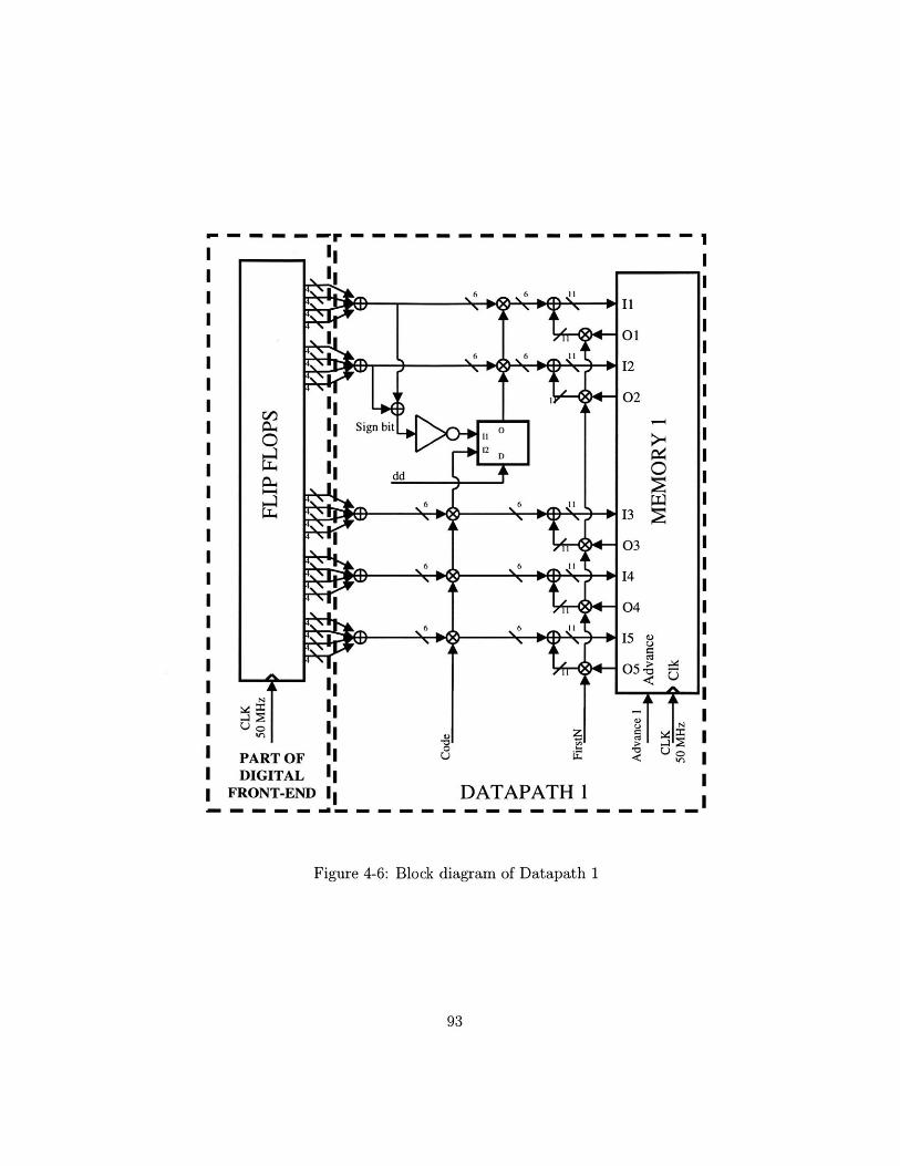
I= - - - - - r - - - - - 1
0n
Qo
L
6
iT
IiIiIiI. 01
UPART OF 1DIGITAL
FRONT-END Ii
z
DATAPATH 1
Figure 4-6: Block diagram of Datapath 1
93
Ii
01
12
02
13
C
6 6
Sign bit0
dd
03
14
04
15 8
05-O
6
x- - - - - M
IIIIIIII
.4 I~ I
I~ I.4
-4 IIIIIII
II
-~ IQol
II
=0

- ---- -- - --- -------
Ii
0n
IIIIIIIIIIIIIIIIIIIIIL
6 6 1
6 6 Z1
6 6 Z1
66 ,1 I
p- p
11
01
12
02
13
03
14
04
15
05
DIGITALFRONT-END i DATAPATH 2
IUI
IIII
ClII0IIIII
C.) II
<U
IN I
-~ III
Figure 4-7: Block diagram of Datapath 2
94
UA
PART OF

results of the correlations are stored in a memory until they are ready (when N,
values have been added). The operation of this memory block changes from coarse
acquisition to fine tracking and decision directed fine tracking. In coarse acquisition,
all its positions are used. In fine tracking, only two channels are used. Besides, during
coarse acquisition, both Datapath 1 and Datapath 2 are activated. In fine tracking,
only Datapath 1 is used.
The first task in the correlators is to add the incoming samples in groups of
4 consecutive samples. In this way, the integration window of 2 ns is effectively
implemented and the bit rate is reduced 2
Then, these numbers are multiplied by the code (if the state of the receiver is
coarse acquisition or fine tracking) or by the sign of the bit detected (if the state of
the receiver is decision directed fine tracking). This is the reason for the difference
between Datapath 1 and Datapath 2. Datapath 1 includes a block that performs
the hard decision on the bit encoded in an individual pulse while Datapath 2 does
not. The correlation integrates N, = 31 pulses. This will be slightly corrected taking
into account the time that takes to perform some of the calculations in the coarse
acquisition and fine tracking subsystems.
4.5.2 Fine tracking
Although fine tracking happens after coarse acquisition, due to the complexity of
coarse acquisition and the fact that most of the structure in the fine tracking subsys-
tem is reused in the coarse acquisition process, it is necessary to describe its operation
first.
The operations that need to be performed by this subsystem are:
1. Estimation of the delay:
1[n] K (12 - 1) (4.1)(I2 +11)
2For each four samples of 4 bits, only a number of six bits per second is obtained.
95

2. Checking the system has not lost track of the signal:
|I2 + I1| > Thfine (4.2)
where Thfine is a threshold that is fixed using the data from chapter 2. In
presence of signal the probability of not meeting this threshold is low (0.05 or
less) while in presence of only noise it is in the order of 0.5.
3. Updating the values on the loop filter F (z) to obtain the delay update of the
loop.
4. Using the output of the digital filter to obtain the necessary update in the
swapper and the clocks for next iteration of the system.
The signals at the output of this block indicate if the threshold has been met (Check-
thresh) and provide information for change in the delay of the Digital Front-end
operation in the next iteration (Advance, Delay and Swap).
Figure 4-8 shows a block diagram of the fine tracking subsystem. In the lower
part of this diagram there is the procedure of how the enables for the different blocks
are generated so that they are activated one at a time in a pipelined fashion. The
fine tracking subsystem has two inputs coming from the correlation subsystem. The
first input I, is obtained from the input of the first channel of the memory (Il in
Memory 1 block, from Figure 4-6). The second input comes from the input of the
second channel of the same memory (12 from Figure 4-6). These two inputs are 11
bits wide. There is an enable input that starts the calculations in the block when the
result of the correlation of the whole code or of N, pulses (depending on if the state
is fine tracking or decision directed fine tracking) is present.
If the enable is high from 0 ns to 20 ns, Check Thresh is ready before 100 ns.
The signals that encode the new delay of the receiver for the next iteration (Advance,
Delay and Swap whose exact meaning is described later in this chapter) will be ready
after 120 ns. Figure 4-9 indicates the position of this enable signal (indicated as
Enablej) with respect to the enable and reset of the gold code generator. It is seen in
96

bsute Checkthreshaslue __ Threshold 1'
Advance
ROM Flip-Flop,.; Filter Cday D
.- Ap2. . 0
Figure 4-8: Architecture for the fine tracking subsystem
this figure that the fine tracking block is activated at the same time as the memory is
enabled (right after the gold code generator is enabled). When this block is activated
only Nc - 1 pulses and not Nc have been integrated. This is due to the fact that the
output of the block is ready after 120 ns and misses the next pulse that is only 100
ns apart. The choice is then either to ignore the last pulse for the present iteration
or miss the first pulse of the next iteration. The loss is the same in both cases:
Loss(dB) = 101og Nc (4.3)Nc- 1
For N, = 31 this amount is below 1 dB. The choice is made to ignore the last pulse
of the sequence so that the next sequence starts at the right moment.
97

Group: A
Clk5OMHz =
EnableGC =
ResetGC =
Enablef =
ResetFT =
Figure 4-9: Positionother signals.
t7 = 6054 s t8 = 6234 s:
A000 .6100 .6200.
YLFLVLVLFLFLFLFLIILFLFLFLFLFL
of the Enable of the fine tracking subsystem with respect to
4.5.3 Coarse acquisition subsystem
Once the results of the 50 correlations are obtained, they are analyzed. The pipeline
responsible of this analysis has many stages and sub-blocks. A block diagram of the
subsystem is shown in Figure 4-10. The structure of block Maximum and Threshold
of this figure is shown in Figure 4-11. Finally, Figure 4-12 depicts the block Preprocess
from figure 4-11.
The operations performed in this subsystem are:
1. Taking the absolute value of 50 correlations of the incoming signal with differ-
ently delayed templates.
2. Obtaining the maximum absolute value of the 50 values available.
3. Comparing this maximum value to the threshold of detection. This threshold
have been chosen from the data present in chapter 2, to ensure a minimum
value of probability of correct lock while making the probability of false alarm
98
,; ,25929
ULFUUI

~I3X31dWIf1N *~
U
xvwajqcua ajquug
* 6alvug
6a13u
it I I
anj8A JOAO3am aleu
E 4
E
4-p~quug
ID
]IV
4-9ajquuH
4-lalquug
4--
"113
Figure 4-10: Architecture of the coarse acquisition subsystem
99
L A
Ga£ Ga
ALjAlaGu1
1opqquuajq- jqjqlM
Eajquua
X
Valqu
L A
(x uu
Sajqvu3
NOLIOJ ajqvuu
- a.
0
I i
AL
I I

R .um one
Preproccess
Inputsl
1x15JL t 3 &2
1x15kn r-J
I Preproccess Mai=Inputs2 2
100S, O*tputs1 &27
Figure 4-11: Architecture for the maximum and threshold block
as small as possible. If this threshold is not met, it is deduced that no signal is
present in any of the 50 delays tested, and the coarse acquisition state continues
in next iteration. The result of this comparison will be indicated with signal
Jumptofine to the rest of the system.
4. If the threshold is met, the change from coarse acquisition to fine track must
take place. The two adjacent correlations to that chosen as the maximum are
retrived from an auxiliary memory.
5. The fine tracking algorithm is carried out two times. One with the maximum
and the previous correlation value. The second, with the maximum and the
next correlation value.
6. The total energy contained in the maximum and the previous correlation value
is compared to that contained in the pair comprised by the maximum and the
100

5 1 MainCheck
Inputs W -- y
1 14 outputsl
3 315 2 15 E1 3 Outputs2
Figure 4-12: Architecture for the preprocess block
next correlation value. The pair with the maximum energy is assumed to contain
the pulse and its delay with respect to the beginning of the 100 ns interval is
estimated as needed for the first iteration of the fine tracking state.
Part of the functionality of the fine tracking subsystem is needed in this block
since, when the system jumps from one state to the other, the fine tracking process
must be initialized correctly. Its block diagram is shown in Figure 4-13. The difference
with Figure 4-8 is that the filter is not present because the purpose of this block is
to determine the first output of the filter when all positions in its memory would be
equal to 0.
In Figures 4-10, 4-11 and 4-12, several enable signals for the different subblocks
were indicated. Figure 4-14 depicts the sequence of enable signals for the coarse
acquisition block when coarse acquisition is not achieved. Some of these blocks work
sin wh ed fashion and the enable signals to most of them are active during five
periods of the clock. The signal Jumptofine is ready to use 160 ns after the rising
101
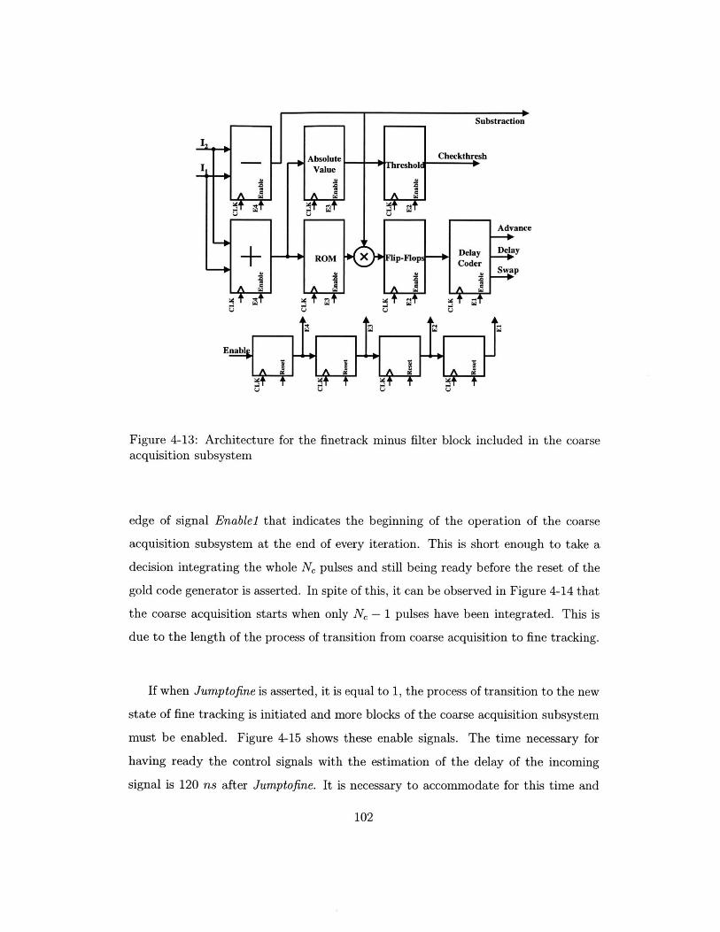
I
Figure 4-13: Architecture for the finetrack minus filter block included in the coarseacquisition subsystem
edge of signal Enablel that indicates the beginning of the operation of the coarse
acquisition subsystem at the end of every iteration. This is short enough to take a
decision integrating the whole N, pulses and still being ready before the reset of the
gold code generator is asserted. In spite of this, it can be observed in Figure 4-14 that
the coarse acquisition starts when only N, - 1 pulses have been integrated. This is
due to the length of the process of transition from coarse acquisition to fine tracking.
If when Jumptofine is asserted, it is equal to 1, the process of transition to the new
state of fine tracking is initiated and more blocks of the coarse acquisition subsystem
must be enabled. Figure 4-15 shows these enable signals. The time necessary for
having ready the control signals with the estimation of the delay of the incoming
signal is 120 ns after Jumptofine. It is necessary to accommodate for this time and
102
Substraction
Absolute Checkthresh- - +aslue Threshold
Advance
ROM X Hp-Fop Delay Delay-+ROM Flip-Flops oer 1
EnSwap
A 0 A QI A Q I

Group: A
Clk50MHz
Enablel
Enable2
Enable3
Enable4
Enable5
Enable6
EnableGC
ResetGC
=0
=0
=0
=0
=0
=0
=0
=0
=0
t9 = 2934 s
92R1 3i nnt6 = 3234 s:
3100m
Figure 4-14: Coarse acquisition subsystem control when no lock is achieved
this implies losing the last pulse in the coarse acquisition iteration and the first two
pulses in the first iteration of the fine tracking state. Since by the time the fine
tracking algorithm starts two pulses have already passed, the gold code generator is
reset using Reset2-GC instead of ResetGC to start the code with its third bit. This
change only affects the first iteration of the fine tracking state.
4.6 Implementation of the delay adjustment
In the previous description, a block that belongs to the Digital Front-end was skipped.
This block is the Swapper, as seen in Figure 4-2. In this section, its functionality and
implementation are described.
4.6.1 Required functionality
The purpose of the swapper is to be able to implement a correction of the beginning
of the integration window of up to 3 samples in any direction (advance 3 samples or
103
,100

:tll = 6334 sr. -inn 4nn
t12 = 6500 s6500
Figure 4-15: Coarse acquisition subsystem control when lock is achieved
discard 3 samples) even if a sequence of corrections of this kind has already happened.
The correction of the delay is given as a 3-bit 2-complement binary number.
In order to clarify the functionality of the Swapper, first it is necessary to indicate
the difference between default window and integration window.
The inputs to the Swapper are the outputs from the analog to digital converter
properly synchronized to a 500 GHz clock edge. Let s, [n] be the data stream coming
from the first ADC, si [n] the samples coming from the second ADC, S2 [n] the stream
coming from the third ADC and s3 [n] the data stream coming from the fourth ADC.
At any even nanosecond 2n, so [n] contains the sample at time 2n+0 ns, si [n] contains
the sample at time 2n + 0.50 ns, S2 [n] contains the sample at time 2n + 1.00 ns and
S3 [n] contains the sample at time n + 1.50 ns. The timing of this stream cannot be
changed, since it is hardwired before the back end. If these samples are grouped for
the same n, the vector [s, [n] , si [n], s2 [n] , S3 [n]] is obtained. Adding the samples in
this vector is equivalent to using an integration window of width 2 ns that starts at
time 2n ns. This is the default window. During coarse acquisition, the Swapper will
104
.6237
Group: A
Clk50MHz
EnableGC
ResetGC
Reset2_GC
Enablea
Enableb
Enablec
Enabled
FineCoarse
Startg
Enabled Hft

deliver this vector to the buffers.
But, after fine tracking starts, corrections to the beginning of the integration
window must be done. In general, the integration window will start at a point m - T,
where T, is the sampling period (500 ps) and m is an integer value'. The nominal time
interval between two consecutive beginnings of interval is equal to N, -Tf/T, samples.
For the values of these parameters used in this receiver, this is equal to 6200 samples.
Let m [i] be the index of the initial sample used in fine tracking iteration i. After one
complete iteration of the algorithm, a correction in delay of d [i] is incorporated so
that the new integration starts in the sample:
m [i + 1] = m [i] + 6200 + d [1] (4.4)
All these numbers are integer numbers. From the sequence m [i], two sequences can
be obtained such that:
m [i] = 4 -n [It] + A [It] (4.5)
with n [i] an integer number and A [i] = mod (m [i] 4). A [i] can only have four
possible values: 0, 1, 2 and 3. A [i] indicates the position of the integration window
with respect to the default window. The buffers from the Digital Front-end require
the data at their input to be already grouped in integration windows that can have
any of these four positions with respect to the default window. The Swapper is
the block that provides at the output the data ordered according to any of the four
possible integration windows, depending on the value of a 2-bit signal called control
that is equal to A [i]. For the different values of control, the vectors at the output of
the Swapper, taking into account the signals at its input, are:
e A [i] = 0 : The integration window uses the samples:
[so [n] , si [ n] ,S2 [n] ,S3 [n]] (4.6)
3 1t can be argued that with the proper sampling and some additional signal processing it can beestimated the result of the integration for any delay fraction of 250 ps, but this implies additionalcomplexity of the receiver.
105

The integration window is then equal to the default window.
. A [i] = 1 : The integration window uses the samples:
[si [n -] , s2 [n- 1] ,S3 [n - 1] , s, [n]] (4.7)
This is equivalent to delaying the integration window 1 sample (500 ps) or
advancing it 3 samples (-1500 ps).
A [i] = 2 : The integration window uses the samples:
[s 2 [n - 1], S3 [n - 1] , s [n] , si [n]] (4.8)
This is equivalent to delaying the integration window 2 samples (1000 ps) or
advancing it 2 samples (-1000 ps).
. A [i] = 3 : The integration window uses the samples:
[s3 [n - 1] , s, [n] , si [n] , S2 [n]] (4.9)
This is equivalent to delaying the integration window 2 samples (1500 ps) or
advancing it 1 sample (-500 ps).
4.6.2 State machine for implementing the change in delay
Trying to express equation (4.4) using equation (4.5):
A i + 1] = mod (m [i] + 6200 + d i], 4) (4.10)
= mod (4 -n [i] + A Ei] + 6200 + d Lu 4)
The multiples of 4 included in the previous expression can be ignored:
A [i + 1] = mod (A [i] + d [i] , 4) (4.11)
106

This equation shows how to update the state of the Swapper based on the previous
control inputs and the delay obtained from the fine tracking subsystem. It necessary
to take into account that:
A [i] + d [i]=4 - k + A [i + 1] (4.12)
Since A [i] can only be equal to 0, 1, 2 and 3, and d [i] can only take the values -3,
-2, -1, 0, 1, 2 and 3, then k can only be equal to -1, 0 or 1. If k = -1 this implies
that the new iteration, apart from a change in the control of the Swapper, needs to
start 2 ns earlier (a complete cycle). If k = 1, the next iteration must start 2 ns later.
It is possible to consider A [i] as the state of the delay in the present iteration, d [i]
as the stimulus of the system, A [2- + 1] as the next state of the delay and k as an
output of the system. Table 4.1 summarizes all the possible changes of state. No cells
are included for the case when the needed increment is zero because in that case the
state does not change. The first line in each of the cells indicates next state, and the
second line, the value of k.
To completely characterize the change in delay, the fine tracking subsystem pro-
vides three signals:
* Swap : Two bits that indicate the new state of the Swapper for the next itera-
tion, used for signal Control in the Swapper.
Table 4.1: Change of state depending on the modification of the delay.
Initial -3 -2 -1 1 2 3State
00 01 10 11 01 10 110 0 0 +1 +1 +1
01 10 11 00 10 11 00-1 -1 -1 0 0 0
10 11 00 01 11 00 01-1 -1 0 0 0 +1
11 00 01 10 00 01 10-1 0 0 0 +1 +1
107

* Advance : Equal to 1 if k = -1, 0 otherwise.
e Delay : Equal to 1 if k - 1, 0 otherwise.
4.6.3 Implementation of the Swapper
Figure 4-16 suggests a possible implementation of the Swapper. It has two blocks:
" Decoder: Depending of the input a different set of signals goes through flip-flops
(are delayed). Depending on the value of the two bits of the signal CONTROL,
the signals that control the multiplexers (C1, C2 and C3) are given in table 4.2.
It is not necessary to use the circuit with a delay (flip-flop) and multiplexer in
the case of ADC'0.
" Reorder block : This can be seen as a multiplexer that does not use most of its
total functionality. In this case it is easier to use a decoder and a set of pass
gates that ensure the connections given in table 4.3. Each output of this block
is assigned a different input. Of the 24 possible combinations only four are used.
It is possible to implement this block without using complete multiplexers.
4.7 Interface of the receiver
This receiver has a limited programmability. Several coefficients used for different
operations are needed:
Table 4.2: Control of C1, C2 and C3 in the reordering circuit, Figure 4-16.
108
Control C1 C2 C300 0 0 001 1 1 110 0 1 111 0 0 0

ADC'O0 A
40
ADC'1 4 D
CLK C1
ADC'2 4 4 OU 40D 1 C
CLK - C2
S0AC'3 44 U
CLK C3
ADC"l ,
ADC"2 4 -
ADC"3 4
Figure 4-16: Proposed architecture for the reordering of the samples
Table 4.3: Connections in the reorder block, Figure 4-16.
Control A B C D00 0 1 2 301 1 2 3 010 2 3 0 111 3 0 1 2
109
I B
REORDERBLOCK
2 C
3 D
CONTROL

" The gold code generator needs four binary vectors, two of them to be used
as initial states of the generator and the other two as the coefficients of the
generating polynomials of the code.
" The filter of the fine track subsystem has five coefficients that are fixed during
the operation of the system.
" A threshold is needed for the detection of coarse acquisition lock and another
is needed for detecting that synchronization lock has been lost.
Registers are used to store these values. In order to program the receiver, a block
that writes the values of these registers is included. This block takes three external
inputs:
* Clock: An external clock that will be used to latched the content of the registers.
" Valid: If this is one, and the clock entry receives a rising edge, a bit is read
from the input Program
" Program: This is the concrete data input. The different bits are loaded in series
through this entry.
The receiver outputs data bits as they are received, both in fine tracking state
(one bit every N, pulses) and in decision directed fine tracking (one bit every pulse).
Two signals are provided: the Data Bit and a Data Clock that is prepared to use its
negative edge to latch the data at the output.
4.8 Summary
In this chapter the architecture for the digital back-end of a base-band UWB receiver
is described. This architecture implements the algorithms described in previous chap-
ters of this thesis. This receiver has two domains, a Digital Front-end working at 500
MHz and a Back-end working at 50 MHz (clock generated from the 500 MHz clock).
The main purposes of the Digital Front-end is to buffer the data coming from the
110

ADC and provide a programmable delay of up to 3 samples in any direction. This last
task is accomplished with a block called swapper. The Back-end is able to perform
the simultaneous correlation of the incoming signal with up to 50 differently delayed
versions of a template. The task of coarse acquisition and fine tracking of the signals
are performed here. This implementation is a full functional back end that allows
some limited programmability.
111

112

Chapter 5
Conclusions
This thesis has developed the digital back-end of an UWB base-band receiver. The
emphasis of the design was placed in the synchronization system. The restrictions
of the design were to achieve an almost completely digital implementation, forcing
the system to deal with an impressive bit rate coming from an ADC providing 2
Gigasamples/s of 4 bits, and to avoid to feed back any signal to the analog system
(concretely to the clock controlling the ADC).
The synchronization process is divided in two parts, coarse acquisition and fine
tracking. Coarse acquisition is a highly non-linear process that provides a first approx-
imation to the delay of the incoming signal. It has been proved that a rectangular
integration window provides a good enough performance not only for rectangular
pulses but also to other kinds. It has been proved the relevance of the probability of
false alarm in the operation of the receiver, revealing that it must be below 1/ (NcNf)
to ensure a reasonable value of Pcd and E[k]. The impact of a difference in frequency
between the transmitter and receiver clocks has been incorporated into the analysis
and it is revealed that for the values usually encountered in quartz oscillators, the
algorithm shown in this thesis is robust.
The fine tracking is implemented using a Delay Locked Loop. Its operation was
analyzed including all the non-idealities associated to the fact that it is wholly im-
plemented in the digital domain. The delay corrections are achieved without any
feedback to the analog clock by using a discrete programmable delay of an integer
113

number of samples. The constraint on the input jitter was related to the width of the
integration window and also to the implementation of the corrections of delay. It is
chosen to implement a delay of up to 3 samples or 1500 ps in any direction, since it
is able to cope with the specifications of the receiver.
Finally, the architecture for the digital back-end of a base-band UWB receiver
implementing the synchronization algorithms was presented. This architecture has
two blocks, a high frequency block working at 500 MHz and a slow frequency block
working at 50 MHz (clock generated from the 500 MHz clock). The high frequency
block buffers the data coming from the ADC and provides the programmable delay
with a block called swapper. The slow frequency domain implements the tracking
algorithms.
5.1 Future work
There are several interesting possibilities:
" The FCC authorized the use of UWB receivers in the band from 3.1 to 10.6
GHz [31. The receivers like the one developed in this thesis are not allowed
because they use a base band signal. Anyway, these circuits can still be used if
correlation with a carrier is placed at some point in the receiver chain and the
correlators are duplicated to implement an in-phase and a quadrature channel.
" The implementation developed here did not take into account power constraints.
It is important to aggressively tackle the task of obtaining a power efficient
implementation of these algorithms.
" Coarse acquisition time can be optimized further, but that implies to be able to
perform more correlations at the same time. This calls for a new architecture
that quite possibly uses mixed signal procedures to obtain the correlation values
of a greater number of delays in parallel.
114

Bibliography
[1] Aether Wire and Location, Inc. Low-Power, Miniature, Distributed Position Lo-
cation and Communication Devices Using Ultra- Wideband, Nonsinusoidal Com-
munication Technology, June 1995.
[2] Braasch, M.S., van Dierendonck, A.J. GPS receiver architectures and measure-
ments. Proceedings of the IEEE, 87(1):48-64, January 1999.
[3] Federal Communications Commission. Ultra- Wideband (UWB) First Report and
Order. February 2002.
[4] Cramer, R.J., Win, M.Z., Scholtz, R.A. Evaluation of the Multipath Charac-
teristics of the Impulse Radio Channel. In IEEE International Symposium on
Personal, Indoor and Mobile Radio Communications, volume 2, pages 864-868,
September 1998.
[5] Dickson, D. and Jett, P. An Application Specific Integrated Circuit Implemen-
tation of a Multiple Correlator for UWB Radio Applications. In Proc. of the
Military Communications Conference, volume 2, pages 1207-1210, 1999.
[6] Gallager, R.G. Discrete Stochastic Processes. Kluwer, 1995.
[7] GEC Plessey Semiconductors. GP1010, Global Positioning Receiver Front End,
Advance Information Data Sheets", April 1994.
[8] GEC Plessey Semiconductors. GP1020, Six-Channel Parallel Correlator Circuit
for GPS or Glonass Receivers, Advance Information Data Sheets, April 1994.
115

[9] Homier, E.A. and Scholtz, R.A. Rapid Acquisition of Ultra Wideband Signals in
the Dense Multipath Channel. In Proc. of the 2002 IEEE Conference on UWB
Systems and Technologies, pages 105-110, March 2002.
[10] Le Martret, C.J. and Giannakis, G.B. All Digital PAM Impulse Radio for Mul-
tiple Access through Frequency Selective Multipath. In Proc. of the IEEE 2000
Global Telecommunications Conference, pages 77-81, 2000.
[11] Le Martret, C.J. and Giannakis, G.B. All Digital PPM Impulse Radio for Mul-
tiple Access through Frequency Selective Multipath. In Proceedings of the 2000
IEEE Sensor Array and Multichannel Signal Processing Workshop, pages 22-26,
2000.
[12] Meyr, H. and Ascheid, G. Synchronization in Digital Communications, Volume
1: Phase-, Frequency-Locked Loops and Amplitude Control. Wiley Interscience,
1990.
[13] Newaskar, P., Blazquez, R., Chandrakasan, A. A/D Precision Requirements for
an Ultra-Wideband Radio Receiver. In Proc. of the 2002 IEEE Workshop on
SIPS, pages 270-275, 2002.
[14] O'Donnell, I., Chen, M., Wang, S., Brodersen, R.W. An Integrated, low-Power,
Ultra-Wideband Trasceiver Architecture for Low-Rate, Indoor Wireless Systems.
In IEEE CAS Workshop on Wireless Communications and Networking, 2002.
[15] Oppenheim, A.V. and Schafer, R.W. Discrete-Time Signal Processing. Prentice
Hall, 1989.
[16] Papoulis, A. Probability, Random Variables and Stochastic Processes. McGraw-
Hill, 1992.
[17] Proakis, J.G. Digital Communications. McGraw Hill Inc, 1983.
[18] Shannon, C.E. A Mathematical Theory of Communication. Bell System Tech-
nical Journal, 27:379-423 and 623-656, 1948.
116

[19] Siwiak, K., Withington, P., Phelan, S. Ultra-wide band radio: the emergence
of an important new technology. In Vehicular Technology Conference 2001, vol-
ume 2, pages 1169-1172, 2001.
[20] Win, M.Z., Scholtz, R.A. Comparisons of Analog and Digital Impulse Radio for
Wireless Multiple-Access Communications. In IEEE International Conference
on Communications, volume 1, pages 91-95, June 1997.
[21] Win, M.Z., Scholtz, R.A. Characterization of Ultra-Wide Bandwidth Wireless
Indoor Channels: A Communication-Theoretic View. IEEE Journal on Selected
Areas in Communications, 20(9):1613-1627, December 2002.
117