design of the power switching networkdesign of the power switching · pdf filedesign of the...
TRANSCRIPT

Design of the Power Switching NetworkDesign of the Power Switching Network
Ruixing Yang 15.01.2009

Outline
Power Gating implementation stylesSleep transistor power network synthesisWakeup in-rush current controlWakeup and sleep latency reduction
The presentation is based on the reference book (M. Keating, et al., Low PowerThe presentation is based on the reference book (M. Keating, et al., Low Power Methodology Manual for System-on-Chip Design, Springer, 2007. ) chapter 14. All the
contents and figures used here are referenced from the book chapter 14.

Power Gating challenges
Power Gating – effective for reducing the leakage power g g g p
in standby or sleep mode.
However:I) Overhead
Silicon area taken by the sleep transistors.Silicon area taken by the sleep transistors.Routing resources for permanent and virtual power networks.Complex power-gating design and implementation processes.
II) Power integrity issues.IR drop on the sleep transistorsGround bounce caused by in-rush wake up current.
III) Wakeup latency.

Ring vs. Grid Style
Coarse grain power gating can be implemented in either a ring or a grid style power network.Ring based switching – place the switches externally to the power gated block effectivelyRing based switching place the switches externally to the power gated block effectively
encapsulating the block with a ring of switches.Grid based switching – the sleep transistors are distributed throughout the power gated region.
Ring Style Sleep Transistor Implementation Grid Style Sleep Transistor Implementation

Ring vs. Grid Style – cont.
Ring style implementation:
Ad t
Grid style implementation
Ad tAdvantages:
Has a less complex power plan than the grid because of the separation of the permanent power network and the virtual power network. The sleep transistors are
Advantages:
The switches in a grid network drive the virtual supply for the short distances compared with ring-style implementation
p pnot mixed with other logic cells.
Has little negative impact on placement and routing in the standard cell area.
Good option for small blocks of logic where
Requires fewer sleep transistors than the ring-style impl. To achieve the same IR drop target.
The permanent power supply is available across the power-down domain areasGood option for small blocks of logic where
the voltage drop across the switch transistors and VVDD mesh can be managed.
Disadvantages:
across the power down domain areas.
It provides somewhat better trickle charge distribution for management of in-rush current.
Has less impact on the area of a powerDoesn’t support retention registers.
Add significant extra area cost compared to a grid approach.
Has less impact on the area of a power gated block.
Disadvantages:
Has impact on standard cell routing and h i l th iphysical synthesis.
Complexity is added to power routing.

Ring vs. Grid Style – cont.
More grid style impl. – Row and Column Grids
1 C l b d it hi (fi i ht) l1. Column based switching (fig. upper right), employs columns of switch cells spaced evenly across the switched design.
Advantage: Each power switch only has to provide power to a small segment of the standard cell row p gthereby minimizing any potential voltage drop.
Disadvantage: Impact the placement optimization, limiting the flexibility of the standard cell placer.
2 Row based switching (fig bottom right)2. Row based switching (fig. bottom right).
Advantage: Optimal solution for distributed switching since the potential impact on the placement engine is limited.
Disadvantage: Impact routing resources in lower layerDisadvantage: Impact routing resources in lower layer metal, which can be avoided by column based approach.

Ring vs. Grid Style – cont.
Selection of the implementation style
The best choice of the impl. depens on:The design being implementedThe library being used and the type of switches available.The library being used and the type of switches available.The technology being targeted and its specific leakage characteristics.The performance and power goals for the design.The use of the legacy or highly optimized IP.
Hybrid Style Implementation
The grid style is implemented at the top-level and ring style is applied to certain power-gated hard macros and/or power domain blocks which have no retention cells.Advantage: Take use of the both implementation styles’ advantages. Disadvantages: more complex power planning. g g

Ring vs. Grid Style – cont.
Recommendations – Ring vs. Grid Style
1. For the design which implements retention cells, select grid style.2. If no retention cells, check the area budget and the need for permanent
power supply in the power-down areas for always-on buffers. p pp y p y3. For the design which has power-gated hard macros, or blocks without
retention logic, select hybrid style.4. For grid-style, use wide straps in permanent power network to reduce
IR dropIR drop.

Header vs. Footer Switch
Header Switch: use a high VT pMOS transistor to control VDD. Footer Switch: use a high VT nMOS transistor to control VSS. oote S tc use a g OS a s s o o co o SSThe selection decision is based on area cost, IR drop constraints, and system architectural issues.
1. Switch Efficiency Consideration
Definition: Switch Efficiency = ratio of drain current in the ON and OFF states (Ion/Ioff)Total Leakage in the switch fabric is mainly determined by the switch efficiency.
90nm High VT pMOS Switch Efficiency 90nm high VT nMOS Switch Efficiencyat Normal Body Bias at Normal Body Bias

Header vs. Footer Switch – cont.
2. Area Efficiency Consideration and L/W ChoiceThe area efficiency depends on the size (L*W) and layout implementation of the sleep t i ttransistors. Optimal L is determined by the switch efficiency and can be obtained from the switch efficiency curve.
The switch efficiency decreases with the increase of W in pMOS transistors, therefore the small W is preferred.p
Figure shows us:
Ion linearly increases with W.
Ion/W becomes constant atIon/W becomes constant at given L and Vbb -> the areaefficiency is determined by the layout implementation ofthe sleep transistors.

Header vs. Footer Switch – cont.
3. Body Bias Considerations
Applying reverse body bias on the sleep transistor can increase the switch efficiency and reduce leakage significantly.
Cost for the reverse body bias in the header switch is significantly smaller than in the footer switch.
Reason:
N-well of the pMOS transistor is readily available for bias tapping in the standard CMOS process. It can be tapped to its own body bias supply as long p pp y pp y gas N-well of the sleep transistor has enough space from the surrounding standard cells’ N-wells.
nMOS transistor does not have a well in the standard CMOS process. It is necessary to create wells for nMOS sleep transistors to allow separate body y p p ybias. higher chip fabrication cost and design complexity & more process variations.
Conclusion: pMOS header is preferable in reverse body bias application.
Header vs. Footer Switch – cont.
4. System Level Design Consideration
In SoC designs, blocks usually communicate in the active-high interface protocols referencing common ground (VSS) as logic “0”. In header switch implementation, all signal nets in power-gated blocks are settled at Vss which is convenient from system design perspective.Header switch avoids potential signal integrity issues and header switch allows p g g ya simple design of a pull-down transistor to isolate power-gated blocks and clamp output signals at logic “0”.
5. Recommendations – Header vs. FooterArea efficiency is main concern: nMOS, which produces higher switch efficiency y , p g yand smaller transistor size. W should be chosen as large as possible for a given cell height.System level design and IP integration: header. Header is more commonly used than footer in power-gating design currently.Choice of sleep transistor can be limited by the availability of the low-leakage p y y gtransistor in a given technology.Minimum standby leakage is main concern: W should be chosen based on high switch efficiency and hence low leakage.W is obtained based on the investigation of area and leakage trade-off.

Rail vs. Strap VDD Supply
Sleep transistors get power supply from the permanent power network (VDD) and deliver it to the virtual power network (VVDD). Two ways to distribute Vdd to the sleep transistors –R il St VDD lRail vs. Strap VDD supply.
1. Parallel Rail VDD DistributionA VDD rail is added to a cell row in parallel with VVDD rail. The sleep transistor gets its permanent power supply by connecting to VDD rails.
Advantages:Advantages: Permanent power supply rail is reachable throughout the design.No restriction on the placement of cells which require connections to permanent power supply.
Disadvantages:Th i l t ti t k t l t t f ti i i VDD ilThe implementation takes at least one trace of routing resources in every row in VDD rail layer.Incurs layer conflict with conventional standard library cells which use the metal 1 layer for cell internal routing.
Rail vs. Strap VDD Supply
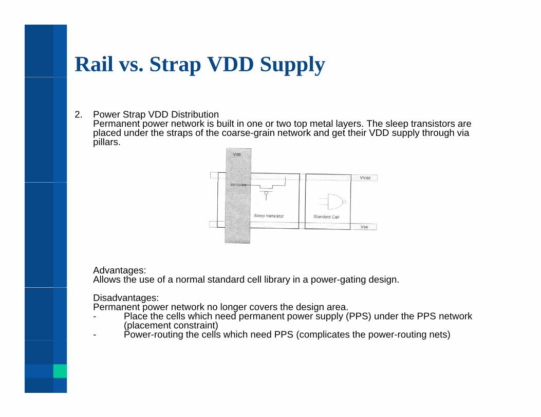
2. Power Strap VDD DistributionPermanent power network is built in one or two top metal layers. The sleep transistors are
l d d th t f th i t k d t th i VDD l th h iplaced under the straps of the coarse-grain network and get their VDD supply through via pillars.
Advantages:Allows the use of a normal standard cell library in a power-gating design.
Disadvantages:Permanent power network no longer covers the design area. - Place the cells which need permanent power supply (PPS) under the PPS network
(placement constraint)- Power-routing the cells which need PPS (complicates the power-routing nets)
Rail vs. Strap VDD Supply
3. Recommendations for supply Distribution
If no available standard cell library which provides extra VDD rail, select power strap VDD.
If impact on routing resources is the main concern, select power strap VDD.
If th i ifi t b f t ti i t i d i d i t it iIf there are a significant number of retention registers in a design and power integrity in power-routing are the main concern, select parallel distribution.

A Sleep Transistor Example
Double row 90nm header switch cell.60 small pMOS transistors of 0 55um width60 small pMOS transistors of 0.55um width.6-row transistor array.Normal body bias.VSS is in the middle of the two rowsA pair of inverters that drive the sleept i t i i l t d i th ll ftransistors is implemented in the cell for area efficiency.

Wakeup Current and Latency Control MethodsMethods
In power gating design, thousands of sleep transistors waking up simultaneous -> a very large current in charging the design to a full power-on state -> IR drop -> functional error / h t t VDD ll t t i t ti i t d i t dshort term VDD collapse -> state in retention registers and memories corrupted.
Possible solution: control in-rush current by separating the chip power supply to many rows and the power is turned on row by row. Disadvantage: crowbar currents -> IR drop. Not practical in power gating design industry.
1. Single Daisy Chain Sleep Transistor Distributiong y pTurn on the sleep transistors gradually by configuring the sleep transistors in a daisy chain style.
Advantages: simple design. Disadvantages: the short delay of the buffers in the chain usually turns on the sleep transistors too quickly -> larger than acceptable in-rush current during wakeup.
2. Dual Daisy Chain Sleep Transistor DistributionU k t i t t t i kl h th d i t t l i h tUse weak transistors to trickle charge the design to prevent large in-rush current. When the design is trickle charged close to VDD, large transistors of the optimal drive strength are turned on.
Wakeup Current and Latency Control MethodsMethods
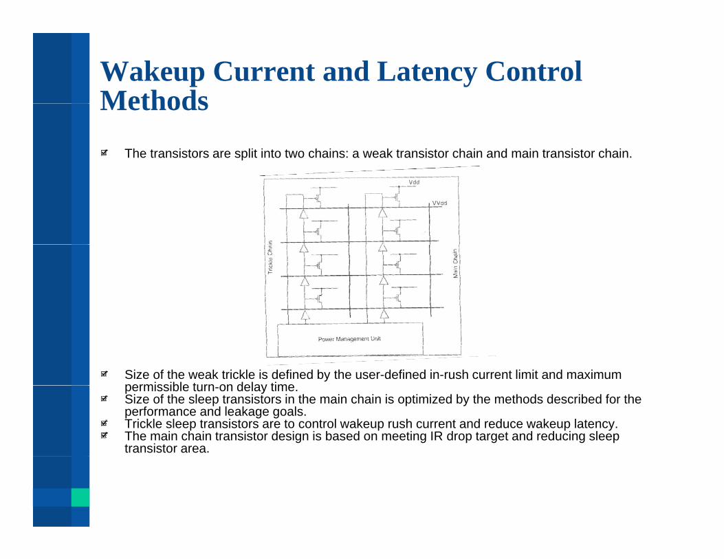
The transistors are split into two chains: a weak transistor chain and main transistor chain.
Size of the weak trickle is defined by the user-defined in-rush current limit and maximum permissible turn on delay timepermissible turn-on delay time.Size of the sleep transistors in the main chain is optimized by the methods described for the performance and leakage goals. Trickle sleep transistors are to control wakeup rush current and reduce wakeup latency. The main chain transistor design is based on meeting IR drop target and reducing sleep transistor area.

Wakeup Current and Latency Control MethodsMethods
3. Parallel Short Chain Distribution of the Main Sleep TransistorWakeup Latency = trickle charge time + turn on time of main chainWakeup Latency trickle charge time + turn on time of main chainReduce main chain turn time to reduce wakeup latency. Single daisy chain -> longest time to charge up & small peak charge current.Parallel array -> smallest delay & largest peak currentCompromise: Parallel short chain – sleep transistors are connected as a number of short daisy h i t d i ll l Th h t d i h i t d i lt lchains connected in a parallel manner. The short daisy chains are turned on simultaneously
when the main chain is turned on. -> The delay is shortened and peak current is controlled.
4. Main Chain Turn-on ControlWhen weak and main chain design are fixed, it is needed to determine the threshold to turn on g ,the main chain. Lower threshold -> turn on early & higher peak current.
5. Buffer Delay Based Main Chain Turn-on ControlControl the time to trickle charge the design to the required threshold. In real power-gating design trickle charge is controlled by the buffer chain which turns on the weak transistors indesign, trickle charge is controlled by the buffer chain which turns on the weak transistors in sequence.

Summary
Power gating design style Ring vs. Grid Implementation of Ring GridImplementation of Ring, GridRow vs. Column GridHybrid Style
Header vs. Footer SwitchS it h ffi iSwitch efficiencyArea efficiencyBody biasSystem level design
R il St VDD lRail vs. Strap VDD supplyParallel Rail vs. Power Strap
Wakeup Current and Latency Control MethodsSingle Daisy ChainSingle Daisy ChainDual Daisy ChainParallel Short Chain Distribution of the Main Sleep TransistorsMain Chain Turn-on Control