design reference of 3w ac-dc power supply 12v output
TRANSCRIPT

MS-PM-03R01
2019.05.08-A/1 Page 1 of 11 MORNSUN Guangzhou Science & Technology Co., Ltd. reserves the copyright and right of final interpretation
Design reference of 3W AC-DC power supply
12V output, input 85-305Vac,
SCM1702ASA & TTLS03-15B12T
Modification Date Version No. Reasons for Revision Model Application Field
2019.04.22 A0 First version SCM1702ASA Industrial control, Smart home ,Instruments
and apparatus
2019.05.08 A/1 Format and content optimization SCM1702ASA Industrial control, Smart home ,Instruments
and apparatus
MS-PM-03R01
2019.05.08-A/1 Page 2 of 11 MORNSUN Guangzhou Science & Technology Co., Ltd. reserves the copyright and right of final interpretation
Contents
1. Overview ........................................................................................................................................................................................................... 3
2. Input & Output Specifications .................................................................................................................................................................. 3
3. Schematic Circuit Diagram .......................................................................................................................................................................... 4
4. Bill of material ............................................................................................................................................................................................ 5
5. Test Data.......................................................................................................................................................................................................... 6
5.1. Input Specifications ........................................................................................................................................................................ 6
5.1.1. No Load Power Consumption .................................................................................................................................................. 6
5.1.2. No Load Power Consumption .................................................................................................................................................. 6
5.2. Output Specifications ...................................................................................................................................................................... 6
5.2.1. Output Voltage&Output Current .......................................................................................................................................... 6
5.2.2. Linear Regulation&Load Regulation .................................................................................................................................. 7
5.2.3. Ripple & Noise ........................................................................................................................................................................ 7
5.2.4. Efficiency ................................................................................................................................................................................ 8
5.2.5. Capacitive Load ...................................................................................................................................................................... 9
5.3. Time series Test ................................................................................................................................................................................ 9
5.3.1. Start-up Time&Hold-up Time ................................................................................................................................................ 9
5.4. Protection specification .............................................................................................................................................................. 11
5.4.1. Over-current Protection(OCP) .......................................................................................................................................... 11

MS-PM-03R01
2019.05.08-A/1 Page 3 of 11 MORNSUN Guangzhou Science & Technology Co., Ltd. reserves the copyright and right of final interpretation
1. Overview
This application is a reference design for an isolated AC-DC power supply based on 85-305VAC input and 12V/3W output. It is widely used
in Industrial control, power instrument and meters, smart home and other occasions that have strict requirements on volume, need to meet UL/CE
certification and low requirements on EMC. The circuit scheme adopts flyback circuit to attack, and the control core adopts SCM1702ASA chip
independently developed by our company. Its peripheral circuit is simple and has certain advantages in cost. In terms of performance, the chip has a
built-in 700V high-voltage start circuit that can start the controller in a wide input voltage range .After starting, the start circuit is closed to reduce the
loss of controller. At the same time, the output over-voltage protection circuit, FB pin fault protection, CS pin fault protection and over-temperature
protection are also integrated to meet the safety requirements.
2. Input & Output Specifications
Input Specifications
Item Operating Conditions Min Typ Max Unit
Voltage AC Input 85 -- 305 VAC
DC Input 70 -- 430 VDC
Input Current Vin=115VAC -- -- 0.12
A Vin=277VAC -- -- 0.06
No Load Power Consumption Vin=230V -- -- 0.25 W
Output Specifications
Item Operating Conditions Min Typ Max Unit
Output Voltage Input voltage range 11.40 12.00 12.60 V
Output Current Input voltage range -- -- 0.25 A
Output Power Input voltage range -- -- 3 W
Ripple & Noise 20MHz bandwidth -- 80 150 mVp-p
Linear Regulation Input voltage variation from low to high at full load -- ±1.5 -- %
Load Regulation 10%-100% load -- ±3.0 -- %
Efficiency nominal input voltage , full load -- 74 -- %
Short-circuit Protection Input voltage range Continuous, self-recovery
Short-circuit Protection 110%-500%Io, self-recovery
Hold-up Time Vin=115VAC -- 10 --
ms Vin=230VAC -- 40 --
Note: * Ripple and noise are measured by “parallel cable” method, please see AC-DC Converter Application Notes for specific operation.
Other Specifications
Item Operating Conditions Min Typ Max Unit
Operating Temperature -40 -- +85 ℃
Isolation Input --Output The test time is 1minute 3000 -- -- VDC
MS-PM-03R01
2019.05.08-A/1 Page 4 of 11 MORNSUN Guangzhou Science & Technology Co., Ltd. reserves the copyright and right of final interpretation
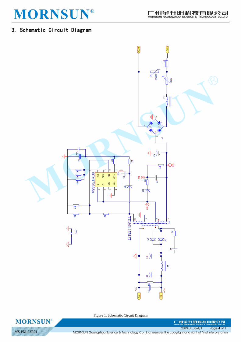
3. Schematic Circuit Diagram
Figure 1. Schematic Circuit Diagram

MS-PM-03R01
2019.05.08-A/1 Page 5 of 11 MORNSUN Guangzhou Science & Technology Co., Ltd. reserves the copyright and right of final interpretation
4. Bill of material
Device description Specification Quantity Position No.
Capacitor 106K/25V/1206/X7R 1.0 C6
Capacitor 271J/250V/0805/NP0 1.0 C1
Resistor 240KΩ 1/4W ±1% 1206 1.0 R2
Resistor 51Ω 1/4W ±1% 1206 1.0 R1
Capacitor 102K/2000V/1206/X7R 1.0 C2
Resistor 4.7KΩ 1/4W ±1% 1206 1.0 R4
Diode 1000V/1A eSGA 1.0 D2
Diode 200V/1.5A/SMA 1.0 D1
IC SCM1702ASA(MOTNSUN) 1.0 U1
Resistor 1KΩ 1/10W ±1% 0603 1.0 R5
Resistor 120Ω 1/8W ±1% 0805 1.0 R3
Resistor 8.2Ω 1/4W ±1% 1206 2.0 R10,R11
Resistor 4.7Ω 1/4W ±1% 1206 1.0 R12
Resistor 680KΩ 1/10W ±1% 0603 1.0 R8
Resistor 17.4KΩ 1/10W ±1% 0603 1.0 R7
Capacitor 104K/50V/0603/X7R 2.0 C3,C5
Resistor 68KΩ 1/10W ±1% 0603 1.0 R6
Resistor 100Ω 1/10W ±1% 0603 1.0 R13
Diode 600V/1A/35ns/1206 1.0 D3
Rectifier bridge 1000V/1.0A/ABS 1.0 D7
Transformer TTLS03-15B12T(MORNSUN) 1.0 T1
Electrical inductance 4.7uH/60mΩ/2.2A 1.0 L2
Safety capacitor Y1/102M/400VAC 1.0 CY1
Fuse wire 2A/300V 1.0 F1
Aluminum electrolytic capacitor 22uF/450V/Φ12.5*20 1.0 C7
Piezoresistor 561K/3500A/10D 1.0 MOV1
NTC Thermistor 10Ω/1A/5D 1.0 NTC1
Inductance 4.7mH/15Ω/0.1A 1.0 L1
Aluminum electrolytic capacitor 100uF/35V/Φ6.3*11 1.0 C9
Solid Capacitor 270uF/16V/Φ8*8 1.0 C8
Terminal 2*Φ1.0/Φ2.0-0.5/9.1 4.0 1,2,3,4
Note: Operating temperature and pressure value depend on the type of the device, and have a lot of to do with PCB layout. MORNSUN IC,
transformer TTLS03-15B12T working temperature; it is recommended to use surface -40-+85℃,TTLS03-15B12T isolation-pressure:3000VAC, the
leakage current is less than 5mA.
MS-PM-03R01
2019.05.08-A/1 Page 6 of 11 MORNSUN Guangzhou Science & Technology Co., Ltd. reserves the copyright and right of final interpretation
5. Test Data
Test Item Test Result
1. Input Specifications
Input Current(230VAC/full load) 42.71mA
No Load Power Consumption(230VAC/no load) 0.14W
2. Output Specifications
Output Voltage 12VDC
Output Current 0.25A
Load Regulation 1.00%
Linear Regulation 0.67%
Ripple & Noise <70mV
Efficiency(230VAC/full load) 76.81%
Capacitive Load >2000uF
3. Time series
Start-up Time(230VAC) 204mS
Hold-up Time (230VAC) 142mS
4. Protection specification
Over-current Protection OK
Short-circuit Protection OK
5.1. Input Specifications
5.1.1. No Load Power Consumption
Operating Conditions: Input voltage variation from low to high at full load, measure input current.
Test Standard:115VAC<0.12A。
Table 1. Input Current(full load)
Input Voltage 85VAC 230VAC 300VAC
Input Current(mA) 80.35 42.71 35.33
5.1.2. No Load Power Consumption
Operating Conditions: Input voltage variation from low to high at no load, measure input power.
Test Standard: <0.25W.
Table 2. No Load Power Consumption
Input Voltage 85VAC 230VAC 300VAC
Input Power(W) 0.08 0.14 0.14
5.2. Output Specifications
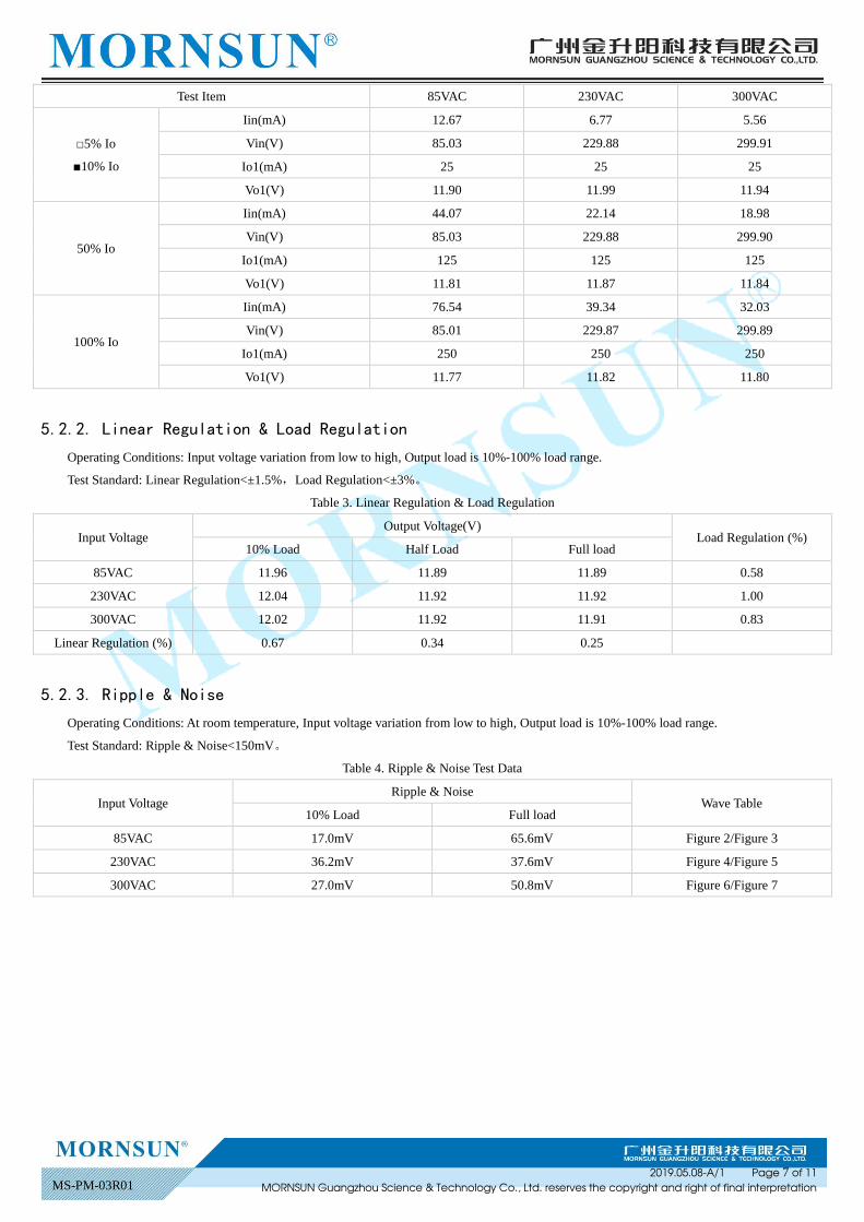
5.2.1. Output Voltage & Output Current
Test Item 85VAC 230VAC 300VAC
0% Io
Iin(mA) 3.27 1.64 1.39
Vin(V) 85.09 229.98 299.91
Vo1(V) 12.04 12.06 11.93
MS-PM-03R01
2019.05.08-A/1 Page 7 of 11 MORNSUN Guangzhou Science & Technology Co., Ltd. reserves the copyright and right of final interpretation
Test Item 85VAC 230VAC 300VAC
□5% Io
■10% Io
Iin(mA) 12.67 6.77 5.56
Vin(V) 85.03 229.88 299.91
Io1(mA) 25 25 25
Vo1(V) 11.90 11.99 11.94
50% Io
Iin(mA) 44.07 22.14 18.98
Vin(V) 85.03 229.88 299.90
Io1(mA) 125 125 125
Vo1(V) 11.81 11.87 11.84
100% Io
Iin(mA) 76.54 39.34 32.03
Vin(V) 85.01 229.87 299.89
Io1(mA) 250 250 250
Vo1(V) 11.77 11.82 11.80
5.2.2. Linear Regulation & Load Regulation
Operating Conditions: Input voltage variation from low to high, Output load is 10%-100% load range.
Test Standard: Linear Regulation<±1.5%,Load Regulation<±3%。
Table 3. Linear Regulation & Load Regulation
Input Voltage Output Voltage(V)
Load Regulation (%) 10% Load Half Load Full load
85VAC 11.96 11.89 11.89 0.58
230VAC 12.04 11.92 11.92 1.00
300VAC 12.02 11.92 11.91 0.83
Linear Regulation (%) 0.67 0.34 0.25
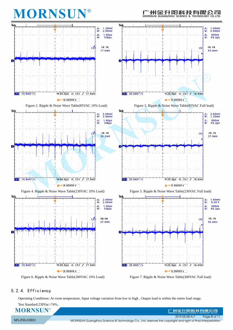
5.2.3. Ripple & Noise
Operating Conditions: At room temperature, Input voltage variation from low to high, Output load is 10%-100% load range.
Test Standard: Ripple & Noise<150mV。
Table 4. Ripple & Noise Test Data
Input Voltage Ripple & Noise
Wave Table 10% Load Full load
85VAC 17.0mV 65.6mV Figure 2/Figure 3
230VAC 36.2mV 37.6mV Figure 4/Figure 5
300VAC 27.0mV 50.8mV Figure 6/Figure 7
MS-PM-03R01
2019.05.08-A/1 Page 8 of 11 MORNSUN Guangzhou Science & Technology Co., Ltd. reserves the copyright and right of final interpretation
Figure 2. Ripple & Noise Wave Table(85VAC 10% Load) Figure 3. Ripple & Noise Wave Table(85VAC Full load)
Figure 4. Ripple & Noise Wave Table(230VAC 10% Load) Figure 5. Ripple & Noise Wave Table(230VAC Full load)
Figure 6. Ripple & Noise Wave Table(300VAC 10% Load) Figure 7. Ripple & Noise Wave Table(300VAC Full load)
5.2.4. Efficiency
Operating Conditions: At room temperature, Input voltage variation from low to high , Output load is within the entire load range.
Test Standard:230Vac>74%。

MS-PM-03R01
2019.05.08-A/1 Page 9 of 11 MORNSUN Guangzhou Science & Technology Co., Ltd. reserves the copyright and right of final interpretation
Table 5. Efficiency
Input Voltage 10%Io Max 25%Io Max 50%Io Max 75%Io Max 100%Io Max Average Efficiency
85VAC 69.77% 77.73% 78.39% 78.47% 77.28% 76.32%
230VAC 59.21% 72.00% 73.94% 75.81% 76.81% 71.55%
300VAC 57.88% 66.26% 72.52% 74.40% 75.40% 69.29%
5.2.5. Capacitive Load
Operating Conditions: At room temperature, Input voltage variation from low to high, Output load is within the entire load range.
Test Standard: Capacitive Load>470uF.
Table 6. Capacitive Load Test Data
Capacitive Load
Input Voltage No Load Wave Table Full load Wave Table
85VAC >2000uF Figure 8 >2000uF Figure 9
230VAC >2000uF -- >2000uF --
300VAC >2000uF -- >2000uF --
Figure 8. No load with 2000uF Capacitive Load (85VAC)
Blue: VIN, Green: Vo
Figure 9. Full load with 2000uF Capacitive Load(85VAC)
Blue: VIN, Green: Vo
5.3. Time series Test
5.3.1. Start-up Time & Hold-up Time
Operating Conditions: Full load
Test Standard: Start-up Time<2S, Hold-up Time>10ms。
Table 7. Start-up Time/Hold-up Time Test Data
Test Item Input Voltage Data Wave Table
Start-up Time
85VAC 206ms Figure 10
230VAC 204ms Figure 11
300VAC 196ms Figure 12
Hold-up Time
85VAC 19.2ms Figure 13
230VAC 142ms Figure 14
300VAC 240ms Figure 15

MS-PM-03R01
2019.05.08-A/1 Page 10 of 11 MORNSUN Guangzhou Science & Technology Co., Ltd. reserves the copyright and right of final interpretation
Figure 10. Power on waveform Blue: VIN ,Green: Vo(85VAC) Figure 13. Power off waveform Blue: VIN, Green: Vo(85VAC)
Figure 11. Power on waveform Blue: VIN, Green: Vo(230VAC) Figure 14. Power off waveform Blue: VIN, Green: Vo(230VAC)
Figure 12. Power on waveform Blue: VIN, Green: Vo(300VAC) Figure 15. Power off waveform Blue: VIN, Green: Vo(300VAC)

MS-PM-03R01
2019.05.08-A/1 Page 11 of 11 MORNSUN Guangzhou Science & Technology Co., Ltd. reserves the copyright and right of final interpretation
5.4. Protection specification
5.4.1. Over-current Protection (OCP)
Operating Conditions: At the lowest, rated, and highest input voltage, the load is gradually increased until the output is turned off.
Test Standard: 110%-500%,self-recovery
Table 8. OCP Test Data
Input Voltage 85VAC 230VAC 300VAC
OCP output current(A) 0.410A 0.410A 0.395A
Recovery current(A) 0.370A 0.376A 0.356A
Figure 16. Protection specification Figure 17. self-recovery
If you have any suggestions or questions about this article, or consult other applications, please contact us [email protected] , we will give
you a detailed answer!
MORNSUN Guangzhou Science & Technology Co., Ltd.
Address: No. 5, Kehui St. 1, Kehui Development Center, Science Ave., Guangzhou Science City, Luogang District, Guangzhou, P. R. China
Tel: 86-20-38601850-8801 Fax: 86-20-38601272 E-mail: [email protected]