design techniques for high-speed low-power wireline receivers · design techniques for high-speed...
TRANSCRIPT

Design Techniques for High-SpeedLow-Power Wireline Receivers
by
Arash Zargaran-Yazd
A THESIS SUBMITTED IN PARTIAL FULFILLMENT OFTHE REQUIREMENTS FOR THE DEGREE OF
DOCTOR OF PHILOSOPHY
in
The Faculty of Graduate Studies
(Electrical and Computer Engineering)
THE UNIVERSITY OF BRITISH COLUMBIA
(Vancouver)
July 2013
c© Arash Zargaran-Yazd 2013

Abstract
High-speed data transmission through wireline links, either copper or optical
based, has become the backbone for modern communication infrastructure.
Since at multi-Gb/s data rates the transmitted signal is attenuated and dis-
torted by the channel, sophisticated analog front-end and/or digital signal
processing are required at the receiver (RX) to recover data and clock from
the received signal.
In this thesis, both analog- and digital-based receivers are investigated, and
power-reduction techniques are exploited at both system- and circuit-levels.
A speculative successive-approximation register (speculative/SAR) digitiza-
tion algorithm is proposed for use at the receiver front-end of digital re-
ceivers that combines equalization and data recovery with the digitization
step at the front-end analog-to-digital converter (ADC). Furthermore, an
architecture for quadrature clock generation is proposed which is of use in
both analog and digital receivers. Then, an analog clock and data recovery
(CDR) architecture suitable for high data rates (e.g., beyond 10 Gb/s) is
proposed that utilizes a wideband data phase generation technique to facil-
itate mixer-based phase detection. The CDR architecture is implemented
and experimentally validated for a 12.5 Gb/s system. Finally, a mixed-mode
hardware-efficient CDR architecture is proposed that exploits both analog
ii

Abstract
and digital design techniques to reach a robust operation suited for long-haul
optical link communications. Proof-of-concept prototypes of the proposed
RX architectures are designed and implemented in 65 nm and 90 nm CMOS
processes. The prototypes are successfully tested. Note that although indi-
vidual performance merits of the each prototype may not necessarily outper-
form that of the state-of-the-art, however, the prototypes confirm the fea-
sibility of the proposed structure. Furthermore, the proposed architectures
can be used at higher data rates particularly if more advanced technologies
with higher device transit frequency, (fT ), is used.
iii

Preface
I, Arash Zargaran-Yazd, am the principle contributor of all chapters. Profes-
sor Shahriar Mirabbasi who supervised the research has provided technical
consultation and editing assistance on the manuscript. Hooman Rashtian
and Kamyar Keikhosravy have respectively contributed to the design of VCO
and comparator of the prototype chip presented in Chapter 6. As described
below, some of the chapters in this thesis have been written based on the
following published work.
Conference papers:
A. Zargaran-Yazd, S. Mirabbasi, and R. Saleh, “A 10 Gb/s low-power
SerDes receiver based on a hybrid speculative/SAR digitization tech-
nique,” in ISCAS, may 2011, pp. 446 –449 →Chapter 3
A. Zargaran-Yazd and S. Mirabbasi, “A 25 Gb/s full-rate CDR circuit
based on quadrature phase generation in data path,” in ISCAS, May
2012, pp. 317–320 →Chapters 4, and 5
Journal papers:
A. Zargaran-Yazd and S. Mirabbasi, “Low-power design technique
for decision-feedback equalisation in serial links,” Electronics Letters,
iv
Preface
vol. 48, no. 17, pp. 1042–1044, 2012 →Chapter 2
A. Zargaran-Yazd, K. Keikhosravy, H. Rashtian, and S. Mirabbasi,
“Hardware-efficient phase-detection technique for digital clock and
data recovery,” Electronics Letters, vol. 49, no. 1, pp. 20 –22, 3 2013
→Chapter 6
A. Zargaran-Yazd and S. Mirabbasi, “12.5-Gb/s full-rate CDR with
wideband quadrature phase shifting in data path,” Circuits and Sys-
tems II: Express Briefs, IEEE Transactions on, vol. 60, no. 6, pp.
297–301, 2013 →Chapter 5
v

Table of contents
Abstract . . . . . . . . . . . . . . . . . . . . . . . . . . . . . . . . . ii
Preface . . . . . . . . . . . . . . . . . . . . . . . . . . . . . . . . . . iv
Table of contents . . . . . . . . . . . . . . . . . . . . . . . . . . . . vi
List of tables . . . . . . . . . . . . . . . . . . . . . . . . . . . . . . . x
List of figures . . . . . . . . . . . . . . . . . . . . . . . . . . . . . . xi
List of acronyms . . . . . . . . . . . . . . . . . . . . . . . . . . . . xvii
List of symbol definitions . . . . . . . . . . . . . . . . . . . . . . . xix
Acknowledgments . . . . . . . . . . . . . . . . . . . . . . . . . . . xxi
Dedication . . . . . . . . . . . . . . . . . . . . . . . . . . . . . . . . xxiii
1 Introduction . . . . . . . . . . . . . . . . . . . . . . . . . . . . . 1
1.1 Motivation . . . . . . . . . . . . . . . . . . . . . . . . . . . . 1
1.2 Serial-link data transmission and reception . . . . . . . . . . 3
1.3 Clocking schemes in serial links . . . . . . . . . . . . . . . . 6
1.4 Power efficiency of wireline TX and RX . . . . . . . . . . . . 9
vi
Table of contents
1.5 Summary of objectives and contributions . . . . . . . . . . . 11
1.6 Organization of thesis . . . . . . . . . . . . . . . . . . . . . . 12
2 Low-power equalization . . . . . . . . . . . . . . . . . . . . . . 14
2.1 Channel as a low-pass filter . . . . . . . . . . . . . . . . . . . 14
2.2 Inter-symbol interference . . . . . . . . . . . . . . . . . . . . 16
2.3 Channel equalization . . . . . . . . . . . . . . . . . . . . . . 20
2.3.1 Continues-time linear equalizer . . . . . . . . . . . . . 21
2.3.2 FIR filter . . . . . . . . . . . . . . . . . . . . . . . . . 22
2.4 Decision feedback equalization . . . . . . . . . . . . . . . . . 24
2.4.1 Conventional analog DFEs . . . . . . . . . . . . . . . 25
2.4.2 Loop-unrolled DFE . . . . . . . . . . . . . . . . . . . 28
2.5 Proposed adaptive slicing technique . . . . . . . . . . . . . . 28
2.6 Comparison of power-equalization efficiency . . . . . . . . . . 31
2.7 Chapter summary . . . . . . . . . . . . . . . . . . . . . . . . 34
3 Low-power DSP-based RX . . . . . . . . . . . . . . . . . . . . 36
3.1 Quantifying power efficiency in RX . . . . . . . . . . . . . . 37
3.2 ADC performance requirements . . . . . . . . . . . . . . . . 39
3.3 Speculative/SAR digitization algorithm . . . . . . . . . . . . 41
3.4 Implementation of the proposed algorithm . . . . . . . . . . 45
3.4.1 Necessity of SAR cycles . . . . . . . . . . . . . . . . . 51
3.5 Power/resolution trade-off in ADC and DAC . . . . . . . . 53
3.6 Measurement results and comparison . . . . . . . . . . . . . 54
3.7 Chapter summary . . . . . . . . . . . . . . . . . . . . . . . . 58
vii
Table of contents
4 Quadrature clock generation in RX . . . . . . . . . . . . . . 59
4.1 Ring oscillators . . . . . . . . . . . . . . . . . . . . . . . . . . 60
4.2 LC oscillators . . . . . . . . . . . . . . . . . . . . . . . . . . 62
4.2.1 Differential LC oscillators . . . . . . . . . . . . . . . . 62
4.2.2 Quadrature LC oscillators . . . . . . . . . . . . . . . 63
4.3 Phase noise and power trade-off . . . . . . . . . . . . . . . . 63
4.3.1 Phase noise in LC VCO . . . . . . . . . . . . . . . . . 65
4.3.2 Phase noise of ring oscillator . . . . . . . . . . . . . . 66
4.3.3 L(∆ω)-power-area trade-off in ring and LC oscillators 66
4.4 Proposed quadrature clock generator . . . . . . . . . . . . . 67
4.5 Enhancing the power efficiency of QCG . . . . . . . . . . . . 70
4.6 Jitter in QCG block . . . . . . . . . . . . . . . . . . . . . . . 79
4.6.1 Maximizing voltage swing . . . . . . . . . . . . . . . 79
4.6.2 Noise of actives and passives in inverter stage . . . . 83
4.7 Chapter summary . . . . . . . . . . . . . . . . . . . . . . . . 85
5 Analog CDR in high-speed links . . . . . . . . . . . . . . . . 87
5.1 Line codes in serial links . . . . . . . . . . . . . . . . . . . . 87
5.2 Clock recovery using high-Q filter . . . . . . . . . . . . . . . 88
5.3 Monolithic high-Q clock recovery . . . . . . . . . . . . . . . . 90
5.4 PLL-based clock recovery . . . . . . . . . . . . . . . . . . . . 91
5.5 Frequency doubling for mixer-based PD . . . . . . . . . . . . 94
5.6 Implementation of mixer-based PD . . . . . . . . . . . . . . 95
5.7 The proposed CDR architecture . . . . . . . . . . . . . . . . 97
5.8 Design of system-level parameters . . . . . . . . . . . . . . . 100
viii
Table of contents
5.8.1 Loop filter . . . . . . . . . . . . . . . . . . . . . . . . 101
5.8.2 System-level performance . . . . . . . . . . . . . . . . 103
5.9 Calibration phase interpolator . . . . . . . . . . . . . . . . . 106
5.10 Performance of QCG block . . . . . . . . . . . . . . . . . . . 107
5.11 Experimental results . . . . . . . . . . . . . . . . . . . . . . . 110
5.12 Chapter summary . . . . . . . . . . . . . . . . . . . . . . . . 113
6 Hardware-efficient eye monitoring technique for clock and
data recovery . . . . . . . . . . . . . . . . . . . . . . . . . . . . 116
6.1 Digital clock recovery methods . . . . . . . . . . . . . . . . . 117
6.2 Proposed CDR technique . . . . . . . . . . . . . . . . . . . . 118
6.3 Measurement results . . . . . . . . . . . . . . . . . . . . . . . 126
6.4 Chapter summary . . . . . . . . . . . . . . . . . . . . . . . . 126
7 Conclusion . . . . . . . . . . . . . . . . . . . . . . . . . . . . . . 129
7.1 Research contributions . . . . . . . . . . . . . . . . . . . . . 129
7.2 Performance comparison . . . . . . . . . . . . . . . . . . . . 131
7.3 Future work . . . . . . . . . . . . . . . . . . . . . . . . . . . 135
Bibliography . . . . . . . . . . . . . . . . . . . . . . . . . . . . . . . 137
Appendix
A Additional circuit schematics . . . . . . . . . . . . . . . . . . 149
A.1 Comparator . . . . . . . . . . . . . . . . . . . . . . . . . . . 149
A.2 Digital-to-analog converter . . . . . . . . . . . . . . . . . . . 150
ix

List of tables
3.1 Performance Summary and Comparison . . . . . . . . . 57
5.1 Values of loop parameters . . . . . . . . . . . . . . . . . 103
5.2 Performance Summary and Comparison . . . . . . . . . 115
6.1 Phase detection truth table for the arrangement
shown in Fig.6.1b. . . . . . . . . . . . . . . . . . . . . . . . 119
7.1 Selection of CDR architecture based on channel
loss . . . . . . . . . . . . . . . . . . . . . . . . . . . . . . . . 134
x

List of figures
1.1 Trend of global IP traffic based on type of network (a), and
the traffic trend based on type of usage (b). Plotted based
on data provided in [1]. . . . . . . . . . . . . . . . . . . . . . 2
1.2 Historical trend of channel data rates in optical link and Eth-
ernet standards. . . . . . . . . . . . . . . . . . . . . . . . . . . 4
1.3 Visual comparison of the zero skew allowance in parallel links
versus arbitrary skew allowance in serial links. . . . . . . . . . 5
1.4 Typical usage of TX-RX pairs in backplanes and mother-
boards (a), and usage of TX-RX pairs as repeaters in long-
haul optical communication (b). . . . . . . . . . . . . . . . . . 6
1.5 Classification of clocking schemes in serial links. . . . . . . . . 7
1.6 Illustration of various clocking schemes in serial links. . . . . 8
1.7 Trend in power efficiency FoM for TX and RX. . . . . . . . . 10
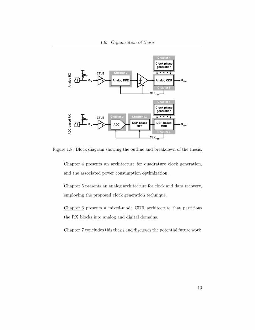
1.8 Block diagram showing the outline and breakdown of the thesis. 13
2.1 Side and top views of a CPW PCB trace. . . . . . . . . . . . 15
2.2 Frequency response of a 10 inch CPW FR4 channel. . . . . . 17
2.3 Simulated impulse response of a band limited FR4 channel . 18
2.4 Eye diagram of 2Gb/s, and 4Gb/s received data patterns. . . 19
xi
List of figures
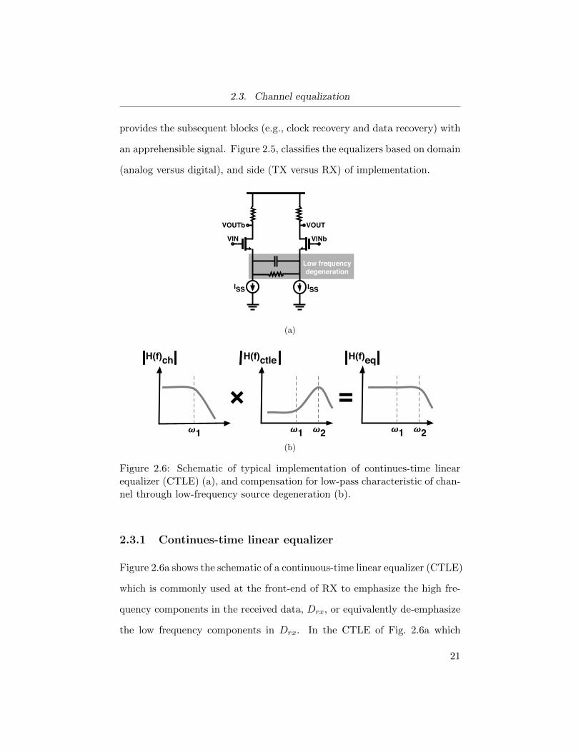
2.5 Classification of equalizers used in high speed links. . . . . . . 20
2.6 Continues-time linear equalizer and its frequency response. . 21
2.7 Equalization using a finite impulse response filter at TX and
RX. . . . . . . . . . . . . . . . . . . . . . . . . . . . . . . . . 23
2.8 A 3-tap ADFE (a), and a (1+2)-tap LUDFE, i.e., the first
tap is unrolled (b). . . . . . . . . . . . . . . . . . . . . . . . . 26
2.9 Illustration of the impulse response of a h0 +h1z−1 +h2z
−2 +
h3z−3 channel. . . . . . . . . . . . . . . . . . . . . . . . . . . 27
2.10 ASDFE technique (a). The gray lines indicate low-speed sig-
nals. SASDFE architecture (b). . . . . . . . . . . . . . . . . . 29
2.11 Comparison of gm,total/WDFE trade-off between ADFE and
ASDFE (a), and between LUDFE and SASDFE (b). . . . . . 32
2.12 Graphical illustration of the block(s) addressed in Chapter 2. 34
3.1 Simplified block diagram of an ADC-based RX. . . . . . . . . 37
3.2 Power consumption versus sampling frequency for ADC’s pub-
lished in literature from 1997 to 2012. . . . . . . . . . . . . . 38
3.3 Illustration of speculative and SAR digitization steps for two
different data patterns. . . . . . . . . . . . . . . . . . . . . . . 41
3.4 The hybrid speculative/SAR digitization algorithm implemented
as a finite state machine. . . . . . . . . . . . . . . . . . . . . . 42
3.5 Block diagram of the proposed DSP-based RX. . . . . . . . . 44
3.6 Schematic of the divide-by-5 circuit . . . . . . . . . . . . . . . 46
3.7 Detailed block diagram of each channel in RX . . . . . . . . . 48
3.8 Timing diagram of the five time-interleaved channels. . . . . . 49
xii
List of figures
3.9 Distribution of the recovered data of each channel, bCHX , to
other channels. . . . . . . . . . . . . . . . . . . . . . . . . . . 51
3.10 Residual ISI in channel impulse response after the speculative
digitization step (a), and the effect of residual ISI in changing
data levels (b). . . . . . . . . . . . . . . . . . . . . . . . . . . 52
3.11 The die micrograph of the prototype implemented in 65-nm
CMOS (a), and the measured eye diagram of the recovered
10 Gb/s data (b). . . . . . . . . . . . . . . . . . . . . . . . . . 56
3.12 Graphical illustration of the block(s) addressed in this Chap-
ter 3. . . . . . . . . . . . . . . . . . . . . . . . . . . . . . . . . 58
4.1 Schematic of a quadrature ring oscillator. . . . . . . . . . . . 60
4.2 Schematic of an LC VCO (a), and canceling the parasitic
resistance of inductor, Rp, in LC tank using an active element
(b). . . . . . . . . . . . . . . . . . . . . . . . . . . . . . . . . . 62
4.3 Quadrature clock generation using two current-coupled LC
oscillators (a), and another method of coupling using a trans-
former (b). . . . . . . . . . . . . . . . . . . . . . . . . . . . . 64
4.4 Quadrature clock generation using coupling a differential VCO
to the quadrature phase generation block. . . . . . . . . . . . 67
4.5 Unilateral coupling through current injection into the QPS
ring. . . . . . . . . . . . . . . . . . . . . . . . . . . . . . . . . 68
4.6 Quadrature clock generator. . . . . . . . . . . . . . . . . . . . 69
xiii
List of figures
4.7 (a) Legend indicating the type and function of inverters used
in QPS and QPC sub-blocks. (b) Format of CML half-inverters
used in QPS and QPC. . . . . . . . . . . . . . . . . . . . . . 70
4.8 QPS sub-block (a), and QPC sub-block (b) in 8× 45 config-
uration. . . . . . . . . . . . . . . . . . . . . . . . . . . . . . . 71
4.9 AC representation of the half CML inverter. . . . . . . . . . . 72
4.10 Simplified model used for delay calculation. . . . . . . . . . . 72
4.11 Speed versus power efficiency of an n-channel device in 90nm
CMOS. . . . . . . . . . . . . . . . . . . . . . . . . . . . . . . 74
4.12 QPS sub-block (a), and QPC sub-block (b) in 8× 90 config-
uration. . . . . . . . . . . . . . . . . . . . . . . . . . . . . . . 76
4.13 Delay of inverter as a function of v∗. . . . . . . . . . . . . . . 77
4.14 Power consumption of the inverter as a function of v∗. . . . . 78
4.15 Effect of using a discrete load capacitance, CL, on power con-
sumption per inverter stage. . . . . . . . . . . . . . . . . . . . 78
4.16 DC-coupled connection between the inverter stages. . . . . . 80
4.17 AC-coupled connection between the inverter stages. . . . . . . 82
4.18 Graphical illustration of the block(s) addressed in this Chap-
ter 4. . . . . . . . . . . . . . . . . . . . . . . . . . . . . . . . . 85
5.1 Comparison of RZ data, NRZ data, and the baud rate clock. 88
5.2 The harmonics around fbaud in the spectrum of NRZ data,
which are used to extract the baud-rate clock. . . . . . . . . . 89
5.3 Block diagram showing the concept of high-Q filter based
clock recovery . . . . . . . . . . . . . . . . . . . . . . . . . . 90
xiv

List of figures
5.4 Block diagram of the monolithic high-Q CDR. . . . . . . . . 91
5.5 Phase-Interpolator-based CDR (a), conventional method of
generating multiple data phases using delay elements, for
mixer-based phase detection (b), wideband quadrature data
phase generation in the proposed CDR (c). . . . . . . . . . . 92
5.6 Schematic of the mixer used as phase detector. . . . . . . . . 96
5.7 Detailed block diagram of the proposed CDR. . . . . . . . . . 97
5.8 Schematic of the phase shifting mixer. . . . . . . . . . . . . . 98
5.9 Linearized model of the proposed CDR. . . . . . . . . . . . . 100
5.10 Type II, order 2 loop filter, as used in the proposed CDR. . . 102
5.11 Frequency response of the closed loop CDR. . . . . . . . . . . 104
5.12 Step response of the CDR. . . . . . . . . . . . . . . . . . . . . 105
5.13 Frequency locking behavior of the CDR when the DR is switched
from 12.5 Gb/s to 12.6 Gb/s. . . . . . . . . . . . . . . . . . . 105
5.14 Normalized PDCopt as a function of Φoff (a). Variation in
Φopt due to various amounts of channel loss (b). . . . . . . . . 108
5.15 Phase jitter in generated clock phases as a function of inverter
delay variation (a). Jitter performance of QCG versus offset
from f0 (b). . . . . . . . . . . . . . . . . . . . . . . . . . . . . 109
5.16 Comparison of power spectral densities of DX . . . . . . . . . 111
5.17 Die micrograph of the prototype chip implemented in 90-nm
CMOS. . . . . . . . . . . . . . . . . . . . . . . . . . . . . . . 112
5.18 Measured eye diagram of the recovered data. . . . . . . . . . 112
5.19 Measured jitter tolerance. . . . . . . . . . . . . . . . . . . . . 113
xv
List of figures
5.20 Graphical illustration of the block(s) addressed in this Chap-
ter 5. . . . . . . . . . . . . . . . . . . . . . . . . . . . . . . . . 114
6.1 The arrangement of DT i and TH i for comparators in binary
and ADC-based CDRs (a), and the arrangement in proposed
CDR (b). . . . . . . . . . . . . . . . . . . . . . . . . . . . . . 117
6.2 The proposed CDR architecture; shaded blocks and signals
are off-chip. . . . . . . . . . . . . . . . . . . . . . . . . . . . 120
6.3 Phase detection characteristic (a), and frequency detection
characteristic of the proposed CDR (b). . . . . . . . . . . . . 121
6.4 Schematic of phase interpolators. . . . . . . . . . . . . . . . . 123
6.5 Die photo of the prototype chip implemented in 90-nm CMOS.127
6.6 Graphical illustration of the block(s) addressed in this Chap-
ter 6. . . . . . . . . . . . . . . . . . . . . . . . . . . . . . . . . 128
7.1 Comparison of the performance of bang-bang CDR, Linear
CDR, and eye monitoring CDR. . . . . . . . . . . . . . . . . 133
A.1 Block diagram of the CML comparator. . . . . . . . . . . . . 150
A.2 Preamplifier (a), latch (b), and CML-to-CMOS circuits. . . . 151
A.3 Schematic of a 4-bit current steering DAC. . . . . . . . . . . 152
xvi

List of acronyms
ADC analog to digital converter
ADFE analog decision feedback equalizer
ASDFE adaptive slicer decision feedback equalizer
BER bit error rate
CDR clock and data recovery
CPW coplanar wave guide
CTLE continuous time linear equalizer
DAC digital to analog converter
DFE decision feedback equalizer
DLL delay locked loop
DR data rate
DSP digital signal processing
FD frequency detector
FFE feed forward equalizer
FIR finite impulse response
IC integrated circuit
IP internet protocol
ISI inter symbol interference
xvii

List of acronyms
LUDFE loop unrolled decision feedback equalizer
MUX multiplexer
NRZ non return to zero
PCB printed circuit board
PD phase detector
PDC phase detector characteristic
PI phase interpolator
PLL phase locked loop
PSD power spectral density
QCG quadrature clock generator
QPC quadrature phase corrector
QPS quadrature phase splitter
RX receiver
SAR successive approximation register
SASDFE speculative adaptive slicer decision feedback equalizer
SERDES serializer deserializer
TRX transceiver
TX transmitter
UI unit interval
VCO voltage controlled oscillator
XO crystal oscillator
xviii

List of symbol definitions
A signal amplitude
cdd total drain capacitance
cgd gate drain capacitance
cgg total gate capacitance
cgs gate source capacitance
clat lateral capacitance
csub capacitance to substrate
CL load capacitance
CLKH full-rate clock
CLKL sub-rate clock
CLKrec recovered clock
Deq equalized data
Drec recovered data
Drx received data
Dx XORed data
f0 nominal frequency
fbw 3-dB bandwidth frequency
fT unity gain frequency of transistor
gm transistor transconductance
xix
List of symbol definitions
Icpl coupling current
Id drain current
Iss tail current
L inductance
Q quality factor
ro output resistance of transistor
RT termination resistance
tp propagation time
vcursor absolute cursor voltage
vgs transistor gate source voltage
Vo output voltage
vod transistor overdrive voltage
vsw peak voltage swing
vth transistor threshold voltage
λ channel length modulation factor
θ phase error
φI in-phase signal component
φIb in-phase inverted signal component
φq quadrature-phase signal component
φqb quadrature-phase inverted signal component
L phase noise
ω angular frequency
ωn natural angular frequency
τ time constant
xx
Acknowledgments
First and foremost, I want to thank my academic advisor, Professor Shahriar
Mirabbasi, for being my mentor and friend, and for the numerous hours that
he spent guiding me to become a better researcher. I was always amazed by
his intelligence and ability to quickly apprehend the design idea that I had
come up with, point out its shortcomings, and suggest neat modifications.
Without his help, advice, and kindness, reaching this stage would have been
impossible for me.
I am thankful to professors Alen Hu, Marek Syrzycki, Peyman Servati, and
Steve Wilton for serving on my Ph.D. examination committee, and provid-
ing me with valuable comments to my research and thesis.
I want to thank my lab mates, Mohammad Beikahmadi, Kamyar Keikhos-
ravy, Hooman Rashtian, Ahmadreza Farsaei, Pouya Kamalinejad, Nima
Taherinejad, and Parisa Behnamfar for all the technical discussions, and
the fun moments which I had with them.
My heart is full of gratitude for my mother, farther, and sister who gave
me hope and encouragement throughout my adventurous journey towards
the Ph.D. degree. They passionately shared all the pains, excitements, frus-
trations, and eventually the ultimate fruit with me. I am truly indebted to
them. My sister, she kept calling me “Doctor” for the past several years,
xxi

Acknowledgments
which stressed me out every single time I heard that word! as I knew there
was a difficult path in front of me. However, it also reminded me how they
had bet all their hopes over my success, which in turn made me more deter-
mined.
Finally, I am thankful to Nazafarin, for her love and support. She patiently
tolerated the not-so-fun Ph.D. candidate Arash, when I had to stay in the
lab all night to test a chip, or spend the whole weekend to write a paper. I
am so grateful to her.
xxii
Dedication
To my parents
xxiii
Chapter 1
Introduction
1.1 Motivation
Fueled in part by the growing trend of cloud-based computation and storage,
and high-speed wireless data access, the global demand for communication
bandwidth has continued to unprecedentedly increase. It is expected that
by 2016, the global annual data traffic will reach 1.3 zettabytes per year
(1021 bytes per year) or 110.3 exabytes per month (1018 bytes per month).
Such data traffic would be equivalent to transferring all movies ever made
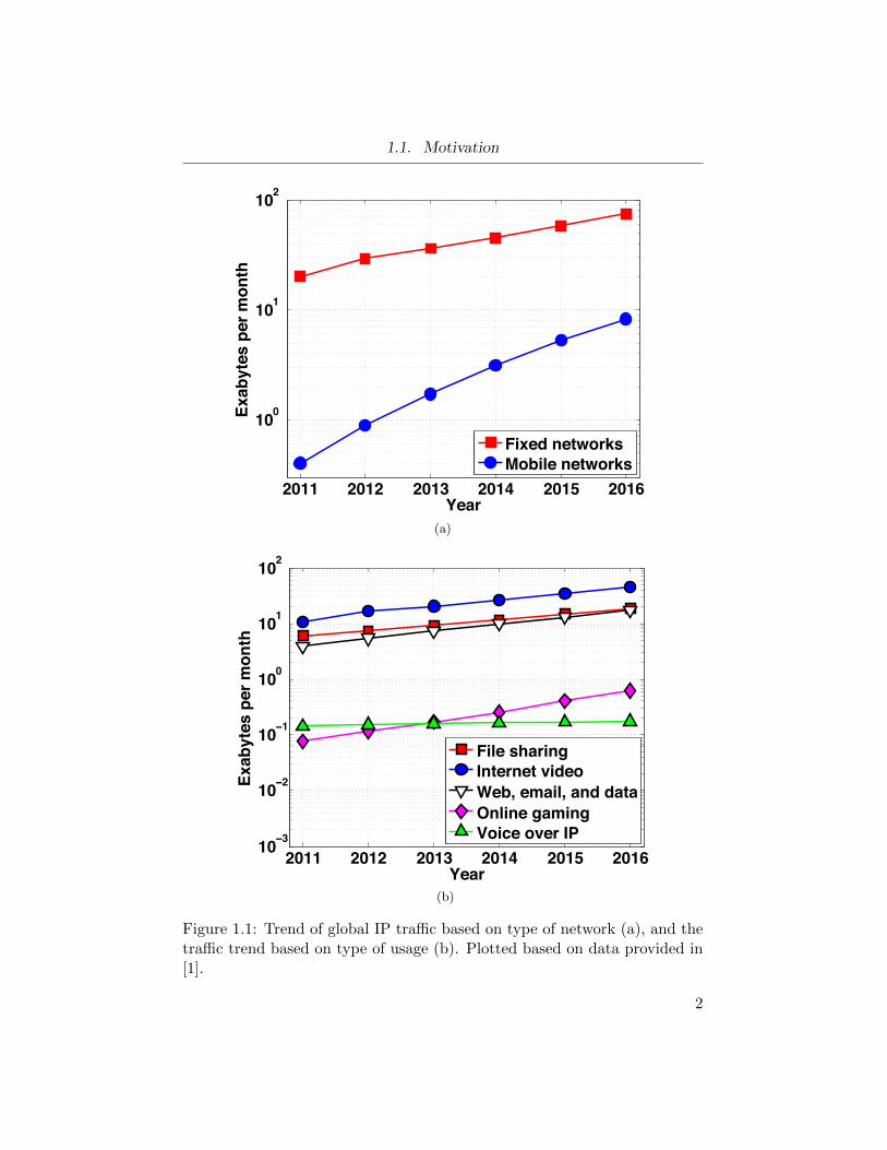
in history every 3 minutes [1]. Figure 1.1a shows the speculated trend in
global internet protocol (IP) traffic growth for fixed and mobile networks.
Figure 1.1b categorizes the total IP traffic based on the type of usage. It
can be observed that the data traffic is expected to increase by roughly
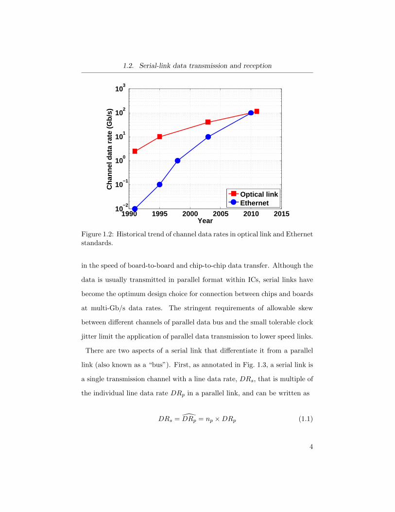
two orders of magnitude by 2016, over a decade period. Figure 1.2 shows
the historical trend of data rates in both optical links and Ethernet stan-
dards. Note that the data rates in these standards are mostly set based on
the trend of the bandwidth demand as illustrated in Fig. 1.1a, rather than
by the speed limits of the available monolithic integrated circuit (IC) tech-
nologies. According to Fig. 1.2, to address the trend in global bandwidth
demand, the most recent standards call for data rates up to 100 Gb/s in the
1
1.1. Motivation
2011 2012 2013 2014 2015 2016
100
101
102
Year
Exab
ytes
per
mon
th
Fixed networksMobile networks
(a)
2011 2012 2013 2014 2015 201610−3
10−2
10−1
100
101
102
Year
Exab
ytes
per
mon
th
File sharingInternet videoWeb, email, and dataOnline gamingVoice over IP
(b)
Figure 1.1: Trend of global IP traffic based on type of network (a), and thetraffic trend based on type of usage (b). Plotted based on data provided in[1].
2

1.2. Serial-link data transmission and reception
backbone wireline channels. While the higher cost of optical modules and
challenges in integration with a monolithic transmitter (TX) and receiver
(RX) increases the overall cost of optical data transmission as compared
to electrical transmission, optical mediums have been historically preferred
in high-speed standards. This is primarily due to the lower high-frequency
loss of an optical medium compared to a metal-based medium (e.g., cop-
per cables). However, as illustrated in Fig. 1.2, the data-rate gap between
optical and electrical (Ethernet) links has been continuously reduced in the
recent years. One major motivation for such trend is the vital role that the
cost factor plays in commercial applications. However, technically this can
be explained by the advancements in the wireline transmitter and receiver
designs which enable high-speed data transmission over lossy and low-cost
electrical channels. Among the TX and RX, the design of a wireline RX can
be more challenging due to the distortion of data in the channel. Addressing
some of the most important trade-offs and challenges specific to the RX is
the goal of this research.
1.2 Serial-link data transmission and reception
The infrastructure of modern wireless and wireline communication systems
is composed of multiple backplanes, each of which having several chips on
them. The connection between different boards and chips is realized through
a series of package I/Os, as well as vias, stubs, connectors and copper traces
drawn on printed circuit boards (PCBs). The ever increasing Ethernet traffic
and prevalence of multicore CPU architectures calls for a substantial increase
3
1.2. Serial-link data transmission and reception
1990 1995 2000 2005 2010 201510
−2
10−1
100
101
102
103
Year
Cha
nnel
dat
a ra
te (
Gb/
s)
Optical linkEthernet
Figure 1.2: Historical trend of channel data rates in optical link and Ethernetstandards.
in the speed of board-to-board and chip-to-chip data transfer. Although the
data is usually transmitted in parallel format within ICs, serial links have
become the optimum design choice for connection between chips and boards
at multi-Gb/s data rates. The stringent requirements of allowable skew
between different channels of parallel data bus and the small tolerable clock
jitter limit the application of parallel data transmission to lower speed links.
There are two aspects of a serial link that differentiate it from a parallel
link (also known as a “bus”). First, as annotated in Fig. 1.3, a serial link is
a single transmission channel with a line data rate, DRs, that is multiple of
the individual line data rate DRp in a parallel link, and can be written as
DRs = DRp = np ×DRp (1.1)
4

1.2. Serial-link data transmission and reception
b14 b13 b12 b11Serial link 2
b24 b23 b22 b21
Parallel link 2 b16 b15 b14 b13
Deserializer
Deserializer
Serial link 1 b26 b25 b24 b23
Serializer
b14 b13 b12 b11 b16 b15
b24 b23 b22 b21b26 b25
Parallel link 1 TXTX
RX
RX
DRs
DRs
DRp
DRp
Figure 1.3: Visual comparison of the zero skew allowance in parallel linksversus arbitrary skew allowance in serial links.
where DRp and np are the total data rate of a parallel link, and the num-
ber of transmission channels (lines) in the parallel link, respectively. The
conversion from multiple channels to a single channel running at a faster
data rate is performed using a serializer. The data on a serial link can be
converted to a parallel format through a deserializer.
Second, a group of data lines in a parallel link are logically differentiated
from a group of serial links through the difference in skew tolerance among
the channels in each of the groups. As shown in Fig. 1.3, by definition, there
is typically a very small (i.e., a fraction of unit interval) tolerance for skew
among the channels in the former group. However, in serial links, there
can be an arbitrary skew among the channels. The freedom in skew, and
a smaller physical footprint of a serial link as compared to a parallel link
have proved advantageous in high-speed data transmission from both cost
and design standpoints.
Figures 1.4a and 1.4b show two common forms of serial data transmission.
In Fig. 1.4a, the transmitter and receiver pairs are typically located in the
5
1.3. Clocking schemes in serial links
SSD core
TX
TX
TX
TX
RX
RX
RX
RX
RX
Solid state drive
GPU core
TX
TX
TX
TX
RX
RX
RX
RX
RX
Graphics processing unit
CPU core
TX TX TX TX
RX
RX
RX
RX
RX
TX
TX
TX
TX
RX
RX
RX
RX
RX
TXTXTXTX
RX
RX
RX
RX
RX
TX
TX
TX
TX
RX
RX
RX
RX
RX
Central processing unit
(a)
RX TX
Repeater
RX TX
RepeaterHigh-loss channel
(b)
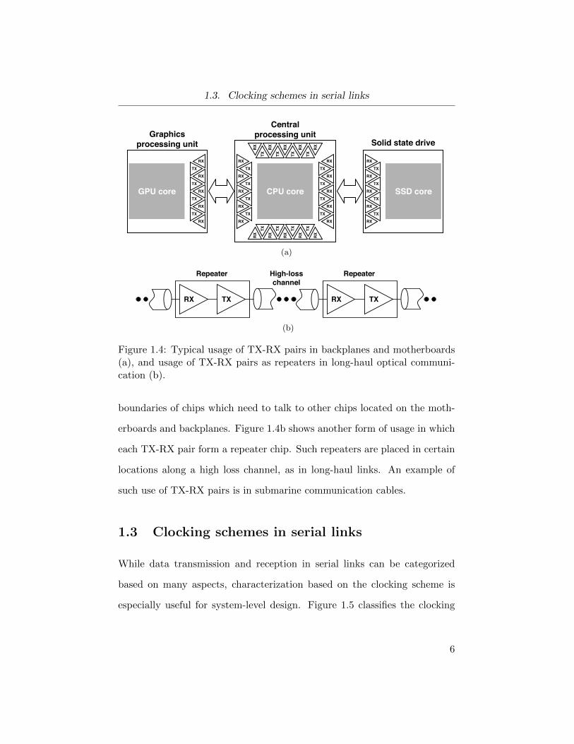
Figure 1.4: Typical usage of TX-RX pairs in backplanes and motherboards(a), and usage of TX-RX pairs as repeaters in long-haul optical communi-cation (b).
boundaries of chips which need to talk to other chips located on the moth-
erboards and backplanes. Figure 1.4b shows another form of usage in which
each TX-RX pair form a repeater chip. Such repeaters are placed in certain
locations along a high loss channel, as in long-haul links. An example of
such use of TX-RX pairs is in submarine communication cables.
1.3 Clocking schemes in serial links
While data transmission and reception in serial links can be categorized
based on many aspects, characterization based on the clocking scheme is
especially useful for system-level design. Figure 1.5 classifies the clocking
6

1.3. Clocking schemes in serial links
Clocking schemes in serial links
Source synchronous CDR-based
Mesochronous
(Phase tracking)
Plesiochronous
(Phase & frequency tracking)
Figure 1.5: Classification of clocking schemes in serial links.
schemes in serial links. In the source synchronous scheme (Fig. 1.6a), the
clock is forwarded along with data from TX to RX. The clock path and
data paths are designed to have equal propagation delays. This insures that
the relative phase offset between data and clock remains constant as they
travel through the matched channels. An active or passive delay element
producing the delay value clkdel is used at RX to align the sampling edge of
the clock to the middle of the data eye. There are two drawbacks associated
with this clocking scheme: First, it is challenging to maintain a constant
clkdel among process, voltage , and temperature (PVT) corners. Second, it
might be challenging or unfeasible to maintain the delay match between the
data and clock channels due to the area constrains imposed by other blocks
and transceivers. Also, the channel incurs different propagation delays for
the data which has broadband frequency characteristic, and the relatively
narrowband clock.
7

1.3. Clocking schemes in serial links
TX RXchdel1
chdel1
Clock synthesizer
XTAL
txdata D Qrecdata
clkdelPLL
D Q
Buffer Buffer
(a)
TX RXchdel1
chdel2
Clock synthesizer
XTAL
txdata D Qrecdata
PLL
D Q
DLL
Buffer Buffer
(b)
chdel1
txda
ta
D Q
recdata
Clock synthesizer
XTALPLL
D Q
Clock recovery
TX side
PLL
EqualizerLine driverRX side
(c)
Figure 1.6: Source synchronous (a), Mesochronous (b), and Plesiochronous(c) clocking schemes in serial links.
A clock and data recovery (CDR) based clocking schemes can be either
Mesochronous, or Plesiochronous. In the Mesochronous scheme (Fig. 1.6b),
clock is still forwarded to RX; however, there is no matching constraint for
the delay of data channel, chdel1, relative to the delay of the clock channel,
chdel2. Therefore, while the clock frequency at RX and TX match, RX needs
a mechanism to recover the correct phase of the sampling clock based on the
received data. Such task is usually performed through a delay-locked loop
8

1.4. Power efficiency of wireline TX and RX
(DLL).
In the Plesiochronous scheme (Fig. 1.6c), only data is sent to RX. Hence,
both TX and RX have their own local clocks. The TX and RX clocks
are both synthesized locally using a phase-locked loop (PLL). However, TX
PLL utilizes a local crystal oscillator (XO) as the reference, while RX uses
the received data as the reference for the clock synthesis PLL. This allows
for arbitrary, yet limited, phase and frequency offset between RX and TX
clocks. Therefore, a Plesiochronous TX-RX pair is more flexible to be used
in applications that do not allow for a separate clock route, or wherever a
perfect match between chdel1 and chdel2 is not possible. While such clocking
scheme doesn’t have the disadvantages mentioned for the source synchronous
method, it comes at the price of complexity and area/power overhead that
CDR imposes on RX. Designing power efficient CDRs at multi Gb/s speeds
is an active area of research.
1.4 Power efficiency of wireline TX and RX
To motivate this work and investigate techniques for enhancing the overall
power efficiency of a serial link, it is helpful to compare the power consump-
tion of TX versus that of RX. A commonly used figure-of-merit (FoM) for
wireline systems is the power efficiency of the link1 which is measured in
mW/(Gb/s) and provides a mean to compare the efficiency of TX, RX, or
the overall transceiver (TRX). The associated FoMs are denoted as FoMTX ,
FoMRX , or FoMTRX , respectively. Figure 1.7a compares the power effi-
1Or similarly, power efficiency of a stand-alone TX or RX.
9
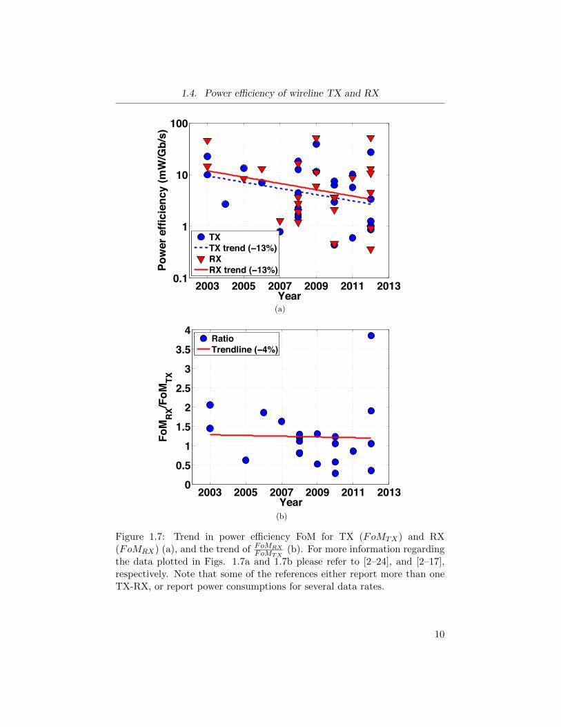
1.4. Power efficiency of wireline TX and RX
2003 2005 2007 2009 2011 20130.1
1
10
100
Year
Pow
er e
ffici
ency
(mW
/Gb/
s)
TXTX trend (−13%)RXRX trend (−13%)
(a)
2003 2005 2007 2009 2011 20130
0.5
1
1.5
2
2.5
3
3.5
4
Year
FoM
RX/F
oMTX
RatioTrendline (−4%)
(b)
Figure 1.7: Trend in power efficiency FoM for TX (FoMTX) and RX(FoMRX) (a), and the trend of FoMRX
FoMTX(b). For more information regarding
the data plotted in Figs. 1.7a and 1.7b please refer to [2–24], and [2–17],respectively. Note that some of the references either report more than oneTX-RX, or report power consumptions for several data rates.
10

1.5. Summary of objectives and contributions
ciency of TX and RX architectures which have been published in the past
decade. The trendline of both FoMTX and FoMRX demonstrate a reduc-
tion of −13% per year. Also, the average power consumption for the RX
block is approximately 15% more than that of the TX block. Note that Fig.
1.7a illustrates results from literature that report either individual TX or
RX, or a TRX. Figure 1.7b shows the ratio FoMRXFoMTX
for the published work
that present a TRX where the power for RX and TX blocks are individually
reported. As the trendline in this figure demonstrates, power consumption
of RXs are on average 25% more than that of the TX. This trend is almost
flat over time which indicates that the RX is typically expected to consume
a larger portion of the overall link power budget. Additionally, given that a
large portion of TX power consumption is due to the requirement of driving
a 25 Ω impedance ( 50 Ω channel || 50 Ω termination) with a certain volt-
age swing dictated by the standard, the power budget of the TX is more
constrained. Therefore, in this research we focus on the RX.
1.5 Summary of objectives and contributions
The main research objectives of this work are as follows:
• Designing a digitization algorithm to address the specific requirements
of low-power multi-Gb/s wireline RX. Currently, the major obstacle
in designing digital high-speed serial link receivers is the power con-
sumption of the front-end baud-rate ADC. The power consumption
and area of a generic full-flash ADC makes its integration into the
receiver a challenging task. To address this issue, we have developed
11

1.6. Organization of thesis
a speculative/SAR ADC which can operate at speeds comparable to
a full-flash ADC, while consuming less power.
• Designing and analyzing the performance and power consumption of
an injection-locked quadrature clock generator. Such block is an inte-
gral part of CDRs that require a quadrature-phase clock in a addition
to the in-phase clock component. Optimizing the power dissipation
of this block is discussed from both circuit-level and system-level per-
spectives.
• Proposing and developing an analog receiver architecture that utilizes
a mixer-based phase detection mechanism to achieve relatively low
power consumption at data rates beyond 10 Gb/s. The CDR comprises
the proposed quadrature clock generator.
• Design of a hardware-efficient mixed-mode eye monitoring technique
for clock and data recovery. The design addresses the power consump-
tion issue from system-level.
1.6 Organization of thesis
Figure 1.8 demonstrates the receiver blocks that are addressed in chapters
of this thesis. Below is the description and breakdown:
Chapter 2 focuses on equalization in both analog and digital RX.
Chapter 3 discusses a digitization algorithm for ADC-based RX.
12
1.6. Organization of thesis
Chapter 4
Chapter 2,3Chapter 3
DrxDSP-based
DFE
RTCTLE
ADC DSP-based CDR Drec
CLKrec
Drx Analog DFE
RTCTLE
Analog CDR Drec
CLKrec
Clock phase generation
Clock phase generation
AD
C-b
ased
RX
Chapter 6
Ana
log
RX
Chapter 4
Chapter 5
Chapter 2
Figure 1.8: Block diagram showing the outline and breakdown of the thesis.
Chapter 4 presents an architecture for quadrature clock generation,
and the associated power consumption optimization.
Chapter 5 presents an analog architecture for clock and data recovery,
employing the proposed clock generation technique.
Chapter 6 presents a mixed-mode CDR architecture that partitions
the RX blocks into analog and digital domains.
Chapter 7 concludes this thesis and discusses the potential future work.
13
Chapter 2
Low-power equalization
The continues scaling of integrated circuits has increased the speed of the
on-chip signal processing. However, the data transmission channels (i.e.
copper wires in printed circuit boards) have roughly stayed the same. Long
gone are the days where the transmission channels were considered ideal
over the bandwidth of signal. In this chapter, first the mechanism of data
distortion due to a lossy channel is described. Then, various methods of data
equalization are introduced. Finally, this Chapter focuses on addressing the
power consumption aspect of decision feedback equalization in high-speed
serial links.
2.1 Channel as a low-pass filter
Due to dielectric loss, skin effects, and parasitic crosstalk with adjacent
channels, the signal observes the channel as a low pass filter, which attenu-
ates the high-frequency components of the transmitted signal, and also adds
deterministic and random noises to it.
Figure 2.1 shows the top and side views of a simple one layer printed
circuit board (PCB). The bottom layer is a grounded conductor (typically
copper) to serve as a global ground, and provide noise isolation. Each layer
14

2.1. Channel as a low-pass filter
G S G
GDielectric G S G
Top viewSide view
Csub
Clat
Figure 2.1: Side and top views of a CPW PCB trace.
of conductor is isolated from the next conductor layer through a dielectric.
As Fig. 2.1 illustrates, the signal trace (S) is shielded from both sides us-
ing ground (G) traces. Such structure forms a coplanar wave guide (CPW)
channel and is useful to reduce crosstalk among different signal traces. How-
ever, such isolation comes at the price of lateral parasitic capacitance, clat,
on the signal line, which degrades the frequency response of the channel.
Also, the parasitic capacitance to the grounded substrate, csub, results in
additional signal loss. For the value of Csub per unit area, csub we can write
csub ∝ε
d(2.1)
where ε and d are the dielectric constant and thickness of dielectric, respec-
tively. Therefore, based on 2.1, to reduce csub, we should either decrease ε
or increase d. Increasing d is not optimal as results in a thicker PCB, and
decreasing ε requires materials that considerably increase the cost of PCB.
15

2.2. Inter-symbol interference
2.2 Inter-symbol interference
The Nyquist criterion states that if the relation given by
T ≥ 1
2×W(2.2)
holds, a Nyquist pulse2 can be transmitted through the channel without be-
ing distorted. Here, T is symbol (bit) duration and W is the channel band-
width. However, while serial link data rates have considerably increased in
the last decade (Fig. 1.2), the bandwidths of the links have not increased at
the same rate and typically we have T 1/(2W ). As the symbol duration
is reduced below the limit defined by the Nyquist criterion, distortion-free
data transmission becomes impossible. To explain the mechanism of data
distortion, we briefly discuss the frequency response of channel.
Figure 2.2 shows the frequency and phase responses of a 10” CPW FR4
channel. The magnitude response of channel resembles that of a low-pass
filter. As a result, the sharp edges in the transmitted waveform would be
observed as rounded curves at the receive side [25].
The phase response indicates that depending on frequency, the various har-
monics of broadband received data experience unequal propagation delays
through the channel. This separates the frequency components of the data
in time domain; hence, partially merging a bit to its pre-cursor and post-
cursor bits. This issue, being described as Inter-symbol interference (ISI),
degrades the quality of the data at the receive side of the channel. Higher
data rates (i.e. shorter T ), or lower channel bandwidth aggravate this prob-
2As an example, a pulse that has a raised-cosine spectra.
16
2.2. Inter-symbol interference
0 5 10 15−75
−50
−25
0
Am
plitu
de a
ttenu
atio
n (d
B)
0 5 10 15 −6pi
−4pi
−2pi
0
Phas
e sh
ift (r
ad)
Frequency (GHz)
S21 phaseS21 magnitude
Frequency (GHz)
Atte
nuat
ion
(dB
)
Phas
e sh
ift (r
ad)
Figure 2.2: Frequency response of a 10 inch CPW FR4 channel.
lem.
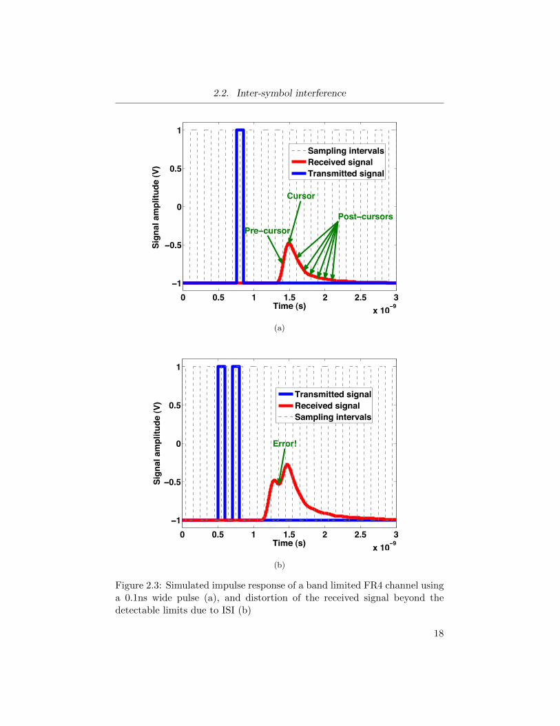
The channel’s impulse response provides and intuitive perspective of how
data gets distorted by the low-frequency characteristic of channel. To gener-
ate such impulse response, we can transmit an isolated ‘1’ which is preceded
and succeeded by a group of ‘0’s and observe the output of channel. Figure
2.3a illustrates this concept. If we sample the impulse response of channel
at each bit interval, the sample with largest amplitude is called cursor, and
the samples with non-zero values before and after the cursor are called pre-
cursor and post-cursor, respectively [26]. Figure 2.3b shows how ISI shifts
the amplitude of the cursor below the decision threshold, and thus bit error
results.
The time-domain responses of the channel in Fig. 2.2 to 2Gb/s, and 4Gb/s
NRZ data are shown in Fig.2.4. As shown in Fig.2.4b, and Fig.2.4d, the
17
2.2. Inter-symbol interference
0 0.5 1 1.5 2 2.5 3x 10 9
1
0.5
0
0.5
1
Time (s)
Sign
al a
mpl
itude
(V)
Sampling intervalsReceived signalTransmitted signal
Pre cursorPost cursors
Cursor
(a)
0 0.5 1 1.5 2 2.5 3x 10 9
1
0.5
0
0.5
1
Time (s)
Sign
al a
mpl
itude
(V)
Transmitted signalReceived signalSampling intervals
Error!
(b)
Figure 2.3: Simulated impulse response of a band limited FR4 channel usinga 0.1ns wide pulse (a), and distortion of the received signal beyond thedetectable limits due to ISI (b)
18

2.2. Inter-symbol interference
10 20 30 40 50
1
0
1
2 Gb/s Signal
Inpu
t sig
nal
Time (ns)
0 10 20 30 40
1
0
1
Time (ns)
Out
put s
igna
l
Differential Output
(a)
In phase Signal
Time (s)
Am
plitu
de (A
U)
0 2 4 6 8x 10 10
1
0.5
0
0.5
1
(b)
5 10 15 20 25
1
0
1
4 Gb/s Signal
Inpu
t sig
nal
Time (ns)
0 5 10 15 20
1
0
1
Time (ns)
Out
put s
igna
l
Differential Output
(c)
In phase Signal
Time (s)
Am
plitu
de (A
U)
0 1 2 3 4x 10 10
1
0.5
0
0.5
1
(d)
Figure 2.4: Simulated response of the band-limited channel of Fig.2.2 alongwith the corresponding eye diagrams using 2Gb/s (a-b), and 4Gb/s (c-d)random data patterns.
channel non-idealities result in small vertical eye opening at the receiver
side and this problem gets aggravated as data rate increases. This makes
the data recovery task more complicated and increases the bit error rate
(BER) of the receiver. Low-pass property of channel does not allow the
channel’s output to properly follow the abrupt changes of transmitted sig-
nal waveform. For a lossy channel without reflections, the smallest vertical
19

2.3. Channel equalization
eye opening typically occurs when an isolated ‘0’ or an isolated ‘1’ is trans-
mitted (i.e., ...00001000... or ...11110111...). Such cases determine the worst
case voltage margin at RX sampler(s), which affects the bit error rate of the
link. If the ISI is large enough, it can completely close the data eye and make
the detection of the transmitted symbols without equalization impossible.
As a result, Different types of equalization are used at both TX and RX to
partially cancel ISI.
Equalization schemes in serial links
TX side RX side
Analog DigitalDigital
Pre-cursor + Post-cursor
FIR filter FFE (FIR filter) DFEDFE CTLE FFE (FIR filter)
Post-cursor
Post-cursor
Pre-cursor + Post-cursor
Pre-cursor + Post-cursor
Pre-cursor + Post-cursor
Figure 2.5: Classification of equalizers used in high speed links.
2.3 Channel equalization
As signal distortion due to ISI is inevitable in high speed links, the data
should be equalized either at TX, RX, or both TX and RX sides. This
20
2.3. Channel equalization
provides the subsequent blocks (e.g., clock recovery and data recovery) with
an apprehensible signal. Figure 2.5, classifies the equalizers based on domain
(analog versus digital), and side (TX versus RX) of implementation.
ISS
VIN VINb
VOUTVOUTb
ISS
Low frequency degeneration
(a)
×!1
H(f)ch
!1 !2
H(f)ctle
!1 !2
H(f)eq
=
(b)
Figure 2.6: Schematic of typical implementation of continues-time linearequalizer (CTLE) (a), and compensation for low-pass characteristic of chan-nel through low-frequency source degeneration (b).
2.3.1 Continues-time linear equalizer
Figure 2.6a shows the schematic of a continuous-time linear equalizer (CTLE)
which is commonly used at the front-end of RX to emphasize the high fre-
quency components in the received data, Drx, or equivalently de-emphasize
the low frequency components in Drx. In the CTLE of Fig. 2.6a which
21

2.3. Channel equalization
utilizes resistive loads, low-frequency components in Drx are attenuated
through reducing the DC gain of the differential stage using source degener-
ation. Considering the simple channel in Fig. 2.6b with low pass frequency
response and 3-dB bandwidth of ω1, the zero in the CTLE frequency re-
sponse, |H(f)ctle|, should be ideally located at ω1 to flatten the overall
equalized frequency response, |H(f)eq|. Note that as |H(f)ctle| can not
sustain an increasing gain till infinite frequency, inevitably the magnitude
response will fall at ω2, where |H(f)ctle| has two poles. To provide a sat-
isfactory equalization at a reasonable power consumption, ω2 should be set
such that
1
2×DR < ω2 <
2
3×DR (2.3)
where DR is the data rate in Gb/s [24].
2.3.2 FIR filter
Figure 2.7a shows the block diagram of a finite impulse response (FIR) filter
as used in TX to pre-emphasis the high frequency contents of transmitted
data, Dtx. Flip flops (FFs) are used to delay the signal for one clock cycle
or equivalently 1 unit interval (UI). Based on channel impulse response, a
weight, Wi is applied to the digital data through an operational transcon-
ductance amplifier (OTA) stage. The overall combination of the FF and
OTA form a filter tap. The taps which precede and succeed the main tap
are called anti-causal taps and causal taps, respectively. Anti-causal taps
(i.e. W−1) are used to cancel pre-cursor components in channel impulse re-
22

2.3. Channel equalization
Q D
RT
W0
W-1
W2
W1 Q D
Q D
Dtx
Q D
1st pre-cursor
Cursor
1st post-cursor
2nd post-cursor
(a)
S/H
Rs
W0
W-1
W2
W1 S/H
S/H
Drx
S/H
1st pre-cursor
Cursor
1st post-cursor
2nd post-cursor
RT
DrecVth
Slicer
(b)
Figure 2.7: Block diagram of FIR filter as used in TX (a), and schematic ofFIR filter as used in RX (b).
sponse; likewise, causal taps are used to cancel the post-cursor components.
Although such filters are simple and inherently fast, their major drawback
is degradation of signal-to-noise ratio (SNR) at the TX node due to the
23

2.4. Decision feedback equalization
limited swing of output stage. In other words, as in CTLE, high frequency
components are emphasized at the price of de-emphasizing low-frequency
components, which translates to a lower SNR.
Figure 2.7b shows the potential implementation of an FIR filter in analog do-
main at RX. Although feasible, FIR filters are rarely implemented in analog
domain. One significant challenge in such implementation is noise enhance-
ment in the sample and hold (S/H) chain. However, in DSP-based RX,
where equalization is performed on the digitized data, FIR filters are com-
monly used before a decision feedback equalizer (DFE) to cancel pre-cursor
taps of channel. Such FIR filters are commonly referred to as a feed-forward
equalizer (FFE) [27].
2.4 Decision feedback equalization
Decision feedback equalizers (DFEs) use the knowledge of previously re-
covered bits to estimate their effect on the current bit, and subtract the
estimated distortion value from the received signal. DFE is a key compo-
nent of high speed3 wireline receivers, and plays a vital role in the emerging
40 to 100 Gb/s links [28]. In channels with a long impulse response tail, can-
celing the post-cursor inter-symbol interference using a DFE is a preferred
choice over a feed-forward equalizer. Such design choice is based on the fact
that unlike FFEs, DFEs do not enhance the noise, or deliberately attenuate
high-frequency components of the received signal [29]. However, DFEs suffer
from stringent requirement for timing closure in the feedback loop within 1
3In this manuscript we refer to data rates > 10 Gb/s as “high speed”.
24
2.4. Decision feedback equalization
unit interval. Depending on the speed and the amount of necessary post-
cursor ISI cancellation, the power consumption of the DFE block may not fit
within the receiver’s power budget [30]. Furthermore, given a certain tech-
nology, the implementation of DFE may not be feasible due to capacitive
self-loading of devices. In this chapter, we propose a DFE implementation
technique which relaxes the trade-off between the power consumption, the
speed, and the amount of post-cursor ISI needed to be canceled.
2.4.1 Conventional analog DFEs
To make a decision, conventional analog DFEs (ADFEs) utilize a static slic-
ing threshold equal to the voltage at the mid-point of the equalized data
eye. Figure 2.8a shows a 3-tap ADFE where using DAC1, the ISI is sub-
tracted from the distorted received signal at the summing node. The result
is compared with the static slicing threshold voltage Vs to recover the data.
Lets consider the channel of Fig. 2.9, whose transfer function is
Hch(z) = h0 + h1z−1 + h2z
−2 + h3z−3 (2.4)
In addition to the cursor h0, the channel impulse response has three post-
cursor components, i.e., h1 to h3. Thus, the total amount of post-cursor ISI
with respect to cursor can be written as
WDFE =|h1|+ |h2|+ |h3|
|h0|(2.5)
To force all post-cursor components to zero, the transconductance of the
25
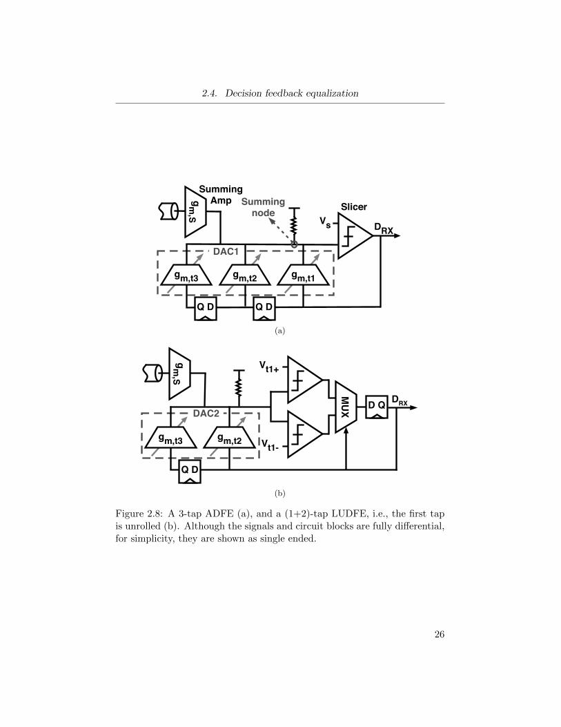
2.4. Decision feedback equalization
DAC1
gm,t1gm,t2gm,t3
Q D Q D
DRXVs
gm,S
Summing Amp SlicerSumming
node
(a)
Vt1-
DRX
Vt1+
MU
X D QDAC2
gm,t2gm,t3
Q D
gm,S
(b)
Figure 2.8: A 3-tap ADFE (a), and a (1+2)-tap LUDFE, i.e., the first tapis unrolled (b). Although the signals and circuit blocks are fully differential,for simplicity, they are shown as single ended.
26

2.4. Decision feedback equalization
h(↑)ch
h0 h1 h3h2
cursor
Figure 2.9: Illustration of the impulse response of a h0 + h1z−1 + h2z
−2 +h3z−3 channel.
summing amplifier, gm,S , and total transconductance of the taps in DAC1,
gm,DAC1, have to be chosen such that:
gm,S =A1ωbw1CL
1−(A1ωbw1
ωT /γ
)︸ ︷︷ ︸
term α
(1 +
2WDFEVcursorvod,t
)︸ ︷︷ ︸
term β
(2.6)
gm,DAC1 =2gm,SWDFEVcursor
vod,t(2.7)
where A1ωbw1, CL, ωT , γ, vod,t, and Vcursor are the gain-bandwidth required
to meet the timing closure at the summing node, input capacitance of the
slicer, the unity-gain frequency of the input devices in the summing am-
plifier, cdd/cgg (i.e., Cdrain/Cgate) of input devices, overdrive voltage of the
tap devices, and the amplitude of the cursor, respectively. Allocating mτ
(m times the time constant of the summing node) for settling, the required
bandwidth is ωbw1 = m/(1UI − tdel1), where tdel1 is the worst-case data
27

2.5. Proposed adaptive slicing technique
propagation delay among taps (usually is the highest for the first tap). In
Eq. 2.6, term α is due to the self loading of the summing amplifier and
termβ introduces the effect of WDFE on self loading of the summing ampli-
fier. The total transconductance required for timing closure gm,total is equal
to gm,DAC1 + gm,S .
2.4.2 Loop-unrolled DFE
Compared to the shift-register flip-flops in Fig. 2.8a, the comparator has a
higher propagation delay as it should resolve a small signal difference to the
full swing. Thus, the overall timing margin for the entire loop is limited
by the small timing margin of the first tap. One well-known remedy is
the loop-unrolled DFE (LUDFE) architecture shown in Fig. 2.8b, in which
the first tap is taken out of the critical path by having two comparators
in parallel. However, this is achieved at the price of the added multiplexer
(MUX) delay and the doubled CL, which in turn may increase the overall
required A1ωbw1 at the summing node [31]. Hence, considering channels
with different first post-cursor h1 (or equivalently the weight of first DFE
tap, t1), this approach does not necessarily decrease DFE’s power penalty
or enhance the timing margin. For the LUDFE shown in Fig. 2.8b, the term
WDFE in Eqs. 2.6 and 2.7 shall be replaced by WDFE − (|h1/h0|).
2.5 Proposed adaptive slicing technique
The proposed adaptive slicer DFE (ASDFE) technique is based on [32] and
is shown in Fig. 2.10a. Here, instead of subtracting the post-cursor ISI from
28

2.5. Proposed adaptive slicing technique
DAC3
gm,P
gm,t1gm,t2
Q D
DRXVs
Lookup Table
gm,t3
Q D
VS Adaption
Pre-Amp
(a)
gm,P
DRX D Q
VS+ Adaption
VS- Adaption
MUX
(b)
Figure 2.10: ASDFE technique (a). The gray lines indicate low-speed sig-nals. SASDFE architecture (b).
the signal itself and performing a bit decision using a static threshold, the
slicer (comparator) threshold Vs is adaptively adjusted in each UI and the
distorted signal coming from the channel is left unaltered. Based on the
29
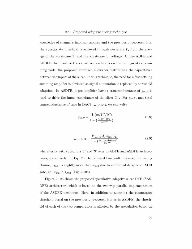
2.5. Proposed adaptive slicing technique
knowledge of channel’s impulse response and the previously recovered bits,
the appropriate threshold is achieved through deviating Vs from the aver-
age of the worst-case ‘1’ and the worst-case ‘0’ voltages. Unlike ADFE and
LUDFE that most of the capacitive loading is on the timing-critical sum-
ming node, the proposed approach allows for distributing the capacitance
between the inputs of the slicer. In this technique, the need for a fast-settling
summing amplifier is obviated as signal summation is replaced by threshold
adaption. In ASDFE, a pre-amplifier having transconductance of gm,P is
used to drive the input capacitance of the slicer CL. For gm,P , and total
transconductance of taps in DAC3, gm,DAC3, we can write
gm,P =A1(m/1UI)CL
1−(A1(m/1UI)
ωT /γ
) (2.8)
gm,DAC3 =WDFEA1ωbw3CL
1−(WDFEA1ωbw3
ωT /γ
) (2.9)
where terms with subscripts ‘1’ and ‘3’ refer to ADFE and ASDFE architec-
tures, respectively. In Eq. 2.9 the required bandwidth to meet the timing
closure, ωbw3, is slightly more than ωbw1 due to additional delay of an XOR
gate, i.e., tdel3 > tdel1 (Fig. 2.10a).
Figure 2.10b shows the proposed speculative adaptive slicer DFE (SAS-
DFE) architecture which is based on the two-way parallel implementation
of the ASDFE technique. Here, in addition to adapting the comparator
threshold based on the previously recovered bits as in ASDFE, the thresh-
old of each of the two comparators is affected by the speculation based on
30
2.6. Comparison of power-equalization efficiency
the two possible bit outcomes ‘0’ or ‘1’. The threshold Vs+ is based on a
speculated value of ‘1’ for the cursor. In the same manner, threshold Vs− is
adjusted based on a speculated cursor value of ‘0’. The main motivation for
having two ASDFE loops in parallel is to enable signal digitization, which
is required by clock recovery (CR) algorithms such as Mueller-Muller [33].
For digitization, Vs+ and Vs− are set below and above the corresponding
speculated cursor voltage levels, respectively. While holding the sampled
signal, the two thresholds are swept in opposite directions in consecutive
search cycles similar to successive approximation ADC (SAR) [32]. How-
ever, unlike the SAR method, the proposed digitization method has a much
smaller search domain and hence a significant speed advantage. Considering
k number of search cycles, Eq. 2.8 can be modified for SASDFE architecture
by using (k×m)/1UI, as the pre-amplifier should settle before the first dig-
itization cycle. Additionally, the capacitive load CL is doubled. Finally, in
Eq. 2.9 we have ωbw4 = (k×m)/(1UI−tdel4), where the term with subscript
‘4’ refers to SASDFE. Note that the parallelism in SASDFE of Fig. 2.10b is
equivalent to 1-tap loop unrolling; therefore, we typically have tdel4 < tdel3.
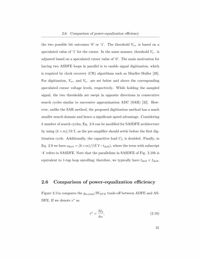
2.6 Comparison of power-equalization efficiency
Figure 2.11a compares the gm,total/WDFE trade-off between ADFE and AS-
DFE. If we denote v∗ as
v∗ =2Idgm
, (2.10)
31

2.6. Comparison of power-equalization efficiency
0 1 2 3 4 5 610
−3
10−2
10−1
100
WDFE
g m,to
tal (
S)
ADFEASDFE
(a)
0 1 2 3 4 5 610
−3
10−2
10−1
100
101
WDFE
g m,to
tal (
S)
LUDFE(t1=0.2)
LUDFE(t1=0.7)
SASDFE(1X full−rate)SASDFE(5X sub−rate)
(b)
Figure 2.11: Comparison of gm,total/WDFE trade-off between ADFE andASDFE (a), and between LUDFE and SASDFE (b).
32
2.6. Comparison of power-equalization efficiency
then, considering that during the design process v∗ is typically chosen to be
a fixed value 4, we would have
Ptotal ∝ gm,total (2.11)
where Ptotal is the total power consumption. Therefore, while the vertical
axis is in units of Siemens, it is also generally proportional to the overall
power consumption.
In ADFE, the power penalty due to WDFE increases considerably if the
amount of post-cursor ISI that needs to be canceled is more than the Vcursor.
Such power penalty can quickly dominate the RX power consumption. On
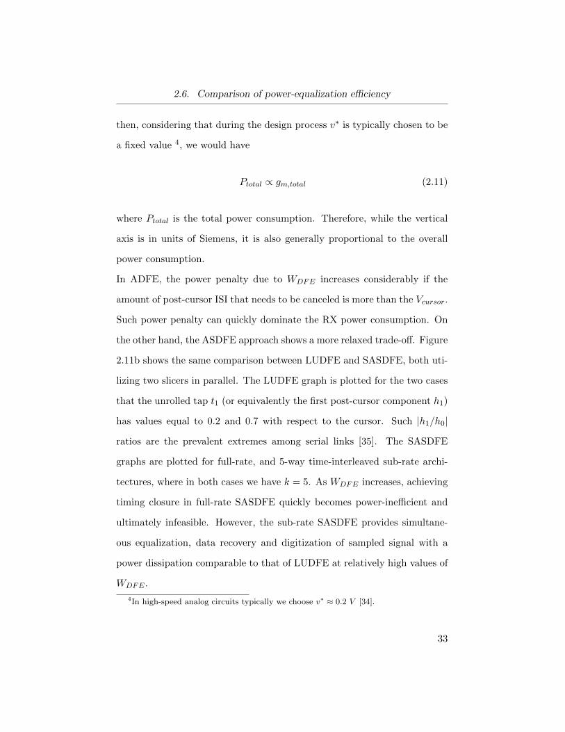
the other hand, the ASDFE approach shows a more relaxed trade-off. Figure
2.11b shows the same comparison between LUDFE and SASDFE, both uti-
lizing two slicers in parallel. The LUDFE graph is plotted for the two cases
that the unrolled tap t1 (or equivalently the first post-cursor component h1)
has values equal to 0.2 and 0.7 with respect to the cursor. Such |h1/h0|
ratios are the prevalent extremes among serial links [35]. The SASDFE
graphs are plotted for full-rate, and 5-way time-interleaved sub-rate archi-
tectures, where in both cases we have k = 5. As WDFE increases, achieving
timing closure in full-rate SASDFE quickly becomes power-inefficient and
ultimately infeasible. However, the sub-rate SASDFE provides simultane-
ous equalization, data recovery and digitization of sampled signal with a
power dissipation comparable to that of LUDFE at relatively high values of
WDFE .
4In high-speed analog circuits typically we choose v∗ ≈ 0.2 V [34].
33

2.7. Chapter summary
2.7 Chapter summary
This chapter
DrxDSP-based
DFE
RTCTLE
ADC DSP-based CDR Drec
CLKrec
Drx Analog DFE
RTCTLE
Analog CDR Drec
CLKrec
Clock phase generation
Clock phase generation
AD
C-b
ased
RX
Ana
log
RX This chapter
Figure 2.12: Graphical illustration of the digital and analog DFE blocksaddressed in this chapter, and their interaction with other RX blocks.
With the emerging high-speed wireline data rates, canceling higher amounts
of post-cursor ISI would be a necessity. As noted on Fig. 2.12, this chapter
investigates the power penalty of canceling a certain amount of post-cursor
ISI taps (WDFE) using DFE. From Fig. 2.12 it can be seen that the equal-
ized signal is used for recovering the data and aligning the sampling edge
of clock to the middle of data eye. While the analog and digital CDR ar-
chitectures proposed in Chapters 5 and 6 do not include a DFE5, it should
be noted that an under-equalized data eye can severely degrade the perfor-
5For the purpose of measurements, high-frequency cables and probes are used to provideinterface to the chip
34
2.7. Chapter summary
mance of the CDR; this is further discussed in Chapter 7. In this Chapter,
the sub-rate SASDFE architecture was proposed, which facilitates canceling
significant amount of post-cursor ISI and simultaneous digitization of sam-
pled data, while avoiding unreasonable power dissipation at RX front-end.
In particular, in high-loss channels that ADFE or LUDFE based RXs may
be impracticable due to excessive power consumption, ASDFE and sub-rate
SASDFE designs provide a relaxed power-equalization trade-off. In Chapter
3, we propose a digital RX architecture which builds on the SASDFE.
35

Chapter 3
Low-power DSP-based RX
While CMOS scaling has been promising to enhance the performance of
digital circuits, from an analog perspective, the performance of N-channel
and P-channel devices has deteriorated in scaled CMOS technologies [34].
Hence, the trend of moving as much as signal processing tasks as possible
from analog domain to digital domain is becoming more and more popular.
Following this trend, advanced high-speed serializer/deserializer (SerDes)
circuits are becoming more DSP-based to take advantage of improved func-
tionality and flexibility of the digital clock and data recovery (CDR) and
equalization [25, 27, 36, 37]. Figure 3.1 shows the simplified block-diagram
of a DSP-based (ADC-based) wireline RX. Usually, a gain block precedes
the ADC to adjust the swing of received signal based on the input range
of ADC. Additionally, as explained in Chapter 2, the gain stage may act
as CTLE to provide high-frequency peaking to partially compensate for ISI.
The digitized signal provided by ADC is processed by succeeding DSP-based
equalization and clock recovery blocks.
As wireline data rates increase in the multi-Gb/s range in the emerging
standards, e.g., IEEE 802.3ba Ethernet standard, sophisticated feed-forward
equalization and decision feedback equalization are needed to compensate
36

3.1. Quantifying power efficiency in RX
DrxDSP-based equalization
RTCTLE
ADC DSP-based CDR Drec
CLKrec
Figure 3.1: Simplified block diagram of an ADC-based RX.
for ISI. Such elaborate equalization translates into tens of FFE and DFE
taps, that if implemented in analog domain, result in a large silicon area
and a high power consumption beyond what can be afforded in a practical
RX. Therefore, the evolution towards a digital architecture seems vital to
enhance the power/area scalability, achieve bit error rates (BERs) equal to
or better than 10−12 under high channel loss [38], and simplify the migration
of circuits to more advanced process technologies.
3.1 Quantifying power efficiency in RX
Although promising, the performance merits of DSP-based receivers is con-
fined by metrics such as power consumption, speed, digitization resolution,
and the impairments of the front-end ADC [25, 37]. Among these issues,
the high power consumption of an ADC operating beyond 10 GS/s is a pro-
hibiting factor to integrate one within an RX. Figure 3.2 shows6 the trade-off
between power consumption and sampling frequency, Fs, of different ADC
architectures, which have been published in literature from 1997 to 2012.
To provide a fair comparison, an FoM is defined for power consumption per
6Plotted based on data from [39].
37

3.1. Quantifying power efficiency in RX
Spee
d ra
nge
of
wire
line
RX
1.E+00!
1.E+01!
1.E+02!
1.E+03!
1.E+04!
1.E+05!
1.E+04! 1.E+05! 1.E+06! 1.E+07! 1.E+08! 1.E+09! 1.E+10! 1.E+11!
FoM
adc (
fJ/c
onv-
step
)!
Fs (Hz)!
ISSCC 2012!
VLSI 2012!
ISSCC 1997-2011!
VLSI 1997-2011!
Figure 3.2: Power consumption versus sampling frequency for ADC’s pub-lished in literature from 1997 to 2012.
conversion step and is defined as follows
FoMadc =Padc
2n × Fs(fJ/conversion step) (3.1)
where n is the digitization resolution. Based on Fig. 3.2, the total power
consumption, Padc, of a 5-bit 10 GS/s ADC which samples the 10 Gb/s
received data, Drx, once every UI (i.e., baud-rate sampling), is given by
Padc > 25 × 10 (GHz)× 500 (fJ/conversion step) = 160 (mW) (3.2)
38
3.2. ADC performance requirements
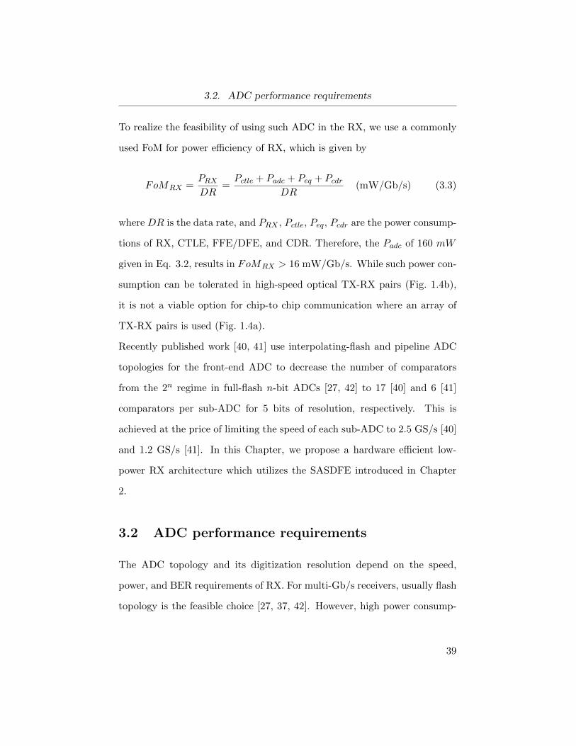
To realize the feasibility of using such ADC in the RX, we use a commonly
used FoM for power efficiency of RX, which is given by
FoMRX =PRXDR
=Pctle + Padc + Peq + Pcdr
DR(mW/Gb/s) (3.3)
where DR is the data rate, and PRX , Pctle, Peq, Pcdr are the power consump-
tions of RX, CTLE, FFE/DFE, and CDR. Therefore, the Padc of 160 mW
given in Eq. 3.2, results in FoMRX > 16 mW/Gb/s. While such power con-
sumption can be tolerated in high-speed optical TX-RX pairs (Fig. 1.4b),
it is not a viable option for chip-to chip communication where an array of
TX-RX pairs is used (Fig. 1.4a).
Recently published work [40, 41] use interpolating-flash and pipeline ADC
topologies for the front-end ADC to decrease the number of comparators
from the 2n regime in full-flash n-bit ADCs [27, 42] to 17 [40] and 6 [41]
comparators per sub-ADC for 5 bits of resolution, respectively. This is
achieved at the price of limiting the speed of each sub-ADC to 2.5 GS/s [40]
and 1.2 GS/s [41]. In this Chapter, we propose a hardware efficient low-
power RX architecture which utilizes the SASDFE introduced in Chapter
2.
3.2 ADC performance requirements
The ADC topology and its digitization resolution depend on the speed,
power, and BER requirements of RX. For multi-Gb/s receivers, usually flash
topology is the feasible choice [27, 37, 42]. However, high power consump-
39

3.2. ADC performance requirements
tion and capacitive loading of a flash ADC make its use in high-speed digital
RX, and the move from conventional binary RX to ADC-based RX, debat-
able [36]. Recently, using SAR topology, promising performance has been
achieved at speeds up to 24 GS/s [43] and 40 GS/s [44] . Nevertheless,
such ADCs do not necessarily consume less power than a full-flash ADC
[45]. As the maximum conversion rate of a single SAR ADC is still less
than 100 MS/s [46], it should be highly interleaved (i.e., 160× in [43]) to
reach sampling rates beyond 10 GS/s. Such immense level of interleaving
results in high area overhead due to peripheral circuitry, and an elaborate
calibration mechanism is needed to cancel the sub-ADC non-idealities to
avoid pattern-noise in ADC array [47]. In our design, by using the proposed
speculative digitization technique in the SAR ADC, we have limited the in-
terleaving factor of the ADC to 5 for a 10 GS/s speed, in 65 nm CMOS.
To determine the sampling frequency of the ADC, a trade-off should be
made between Padc and the amount of information provided to the clock
recovery algorithm (i.e., more information is extracted from Drx in an over-
sampling clock recovery scheme) [40]. In this work, as in [27], the overall
ADC sampling and digitization rate is equal to the baud-rate to achieve a
data recovery rate equal to the highest clock rate in the system. Hence,
Mueller-Muller [33] algorithm would be a candidate for the clock recovery
scheme.
There are several factors such as channel characteristics, and the signaling
scheme that determine the resolution of ADC. In presence of higher amounts
of ISI, the ADC resolution needs to be higher to allow for optimum equal-
ization and clock recovery with the aid of the DSP core. Also, In multi-level
40

3.3. Speculative/SAR digitization algorithm
b(i)= 1
b(i)= 0Speculative Digitization
(DSP)
SAR Digitization
(C2)
SAR Digitization
(C1)
Figure 3.3: Illustration of speculative (solid lines) and SAR digitization steps(dashed lines) for two different data patterns. The two patterns differ in thereceived bit at time=1.1ns.
signaling schemes, the maximum number of signal levels that can be trans-
mitted is confined by the receiver’s ADC resolution [25].
3.3 Speculative/SAR digitization algorithm
Figure 3.3 shows two distorted 10 Gb/s patterns at the RX end of the chan-
nel, which only differ in the bit received at time=1.1 ns. Due to the lowpass
nature of the channel, the received data can no longer maintain the original
voltage levels which are represented by a ‘0’ or a ‘1’. The high-frequency
signal components are filtered out and hence, if a consecutive ‘0’ and ‘1’ pat-
tern is transmitted, the difference in the values of ab(i) (i.e., analog value
41
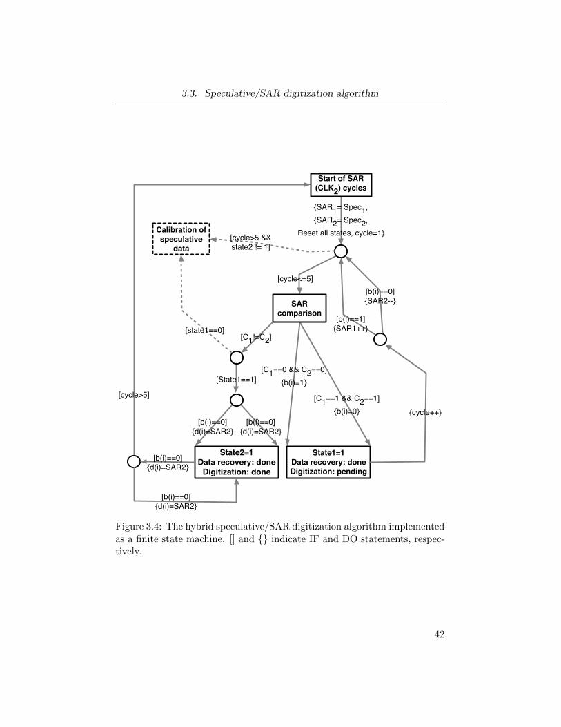
3.3. Speculative/SAR digitization algorithm
Start of SAR (CLK2) cycles
State2=1Data recovery: done
Digitization: done
State1=1Data recovery: doneDigitization: pending
SAR comparison
Calibration of speculative
data
SAR1= Spec1,SAR2= Spec2,
Reset all states, cycle=1
[cycle<=5]
[C1!=C2]
[C1==0 && C2==0]b(i)=1
[C1==1 && C2==1]b(i)=0 cycle++
[State1==1]
[b(i)==0]d(i)=SAR2
[b(i)==0]d(i)=SAR2
[cycle>5 && state2 != 1]
[b(i)==0]d(i)=SAR2
[b(i)==0]d(i)=SAR2
[cycle>5]
[b(i)==0]SAR2--
[b(i)==1]SAR1++[state1==0]
Figure 3.4: The hybrid speculative/SAR digitization algorithm implementedas a finite state machine. [] and indicate IF and DO statements, respec-tively.
42
3.3. Speculative/SAR digitization algorithm
of current sampled bit) and ab(i − 1) are reduced compared to that at the
TX side. The value of ab(i) depends on its preceding bits, as if the channel
has a memory [26]. Hence, if a full-flash ADC is used in the AFE, only a
few comparators will be decisive in digitizing ab(i) at each sampling cycle
of ADC. This is due to the fact that ab(i) will not cross the threshold of the
rest of the comparators. Through the hybrid speculative/SAR digitization
algorithm of Fig. 3.4, we exploit channel’s memory to quickly speculate the
digitized value of each received bit based on the 4 previously recovered bits,
and then use the conventional SAR digitization cycles to fine-tune the specu-
lated value to yield d(i). As shown in the algorithm of Fig. 3.4, a finite state
machine (FSM) uses the speculated value to narrow down the SAR search
domain. The SAR step (dashed horizontal lines in Fig. 3.3) takes over the
speculative step of the algorithm from the points specified by the two spec-
ulated values (solid vertical lines in Fig. 3.3). In this work, due to the fact
that there are typically two separated domains based on either transmitting
a ‘1’ or a ‘0’, two comparators (C1 and C2) are used to perform the SAR
cycles for each of the two cases b(i)=0 or b(i)=1. Breaking the SAR search
domain into two separate paths enhances the speed of digitization and data
recovery functions. As shown in Figs. 3.3 and 3.4, in the speculative step of
the hybrid algorithm, the thresholds of comparators C1 and C2 are simul-
taneously adjusted at the beginning of each SAR sampling cycle. Note that
the thresholds of C1 and C2 are chosen such that they fall below, and above
the speculated analog values for b(i) = 1 and b(i) = 0, respectively. Inter-
estingly, the proposed speculative/SAR digitization algorithm resembles the
SASDFE architecture proposed in Chapter 2. Therefore, as explained in the
43
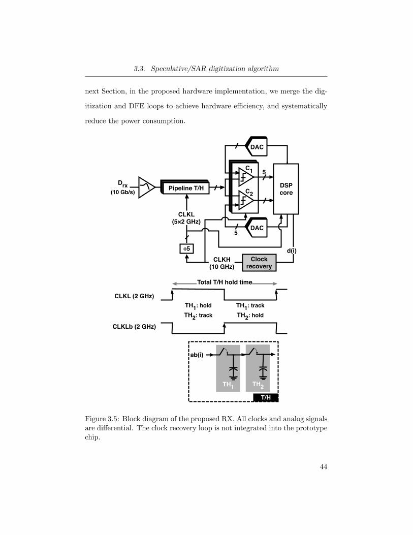
3.3. Speculative/SAR digitization algorithm
next Section, in the proposed hardware implementation, we merge the dig-
itization and DFE loops to achieve hardware efficiency, and systematically
reduce the power consumption.
C1
C1
C1
C1
C1
C1
C1
C1
C1
C2
Drx (10 Gb/s)
5
DACDACDACDACDAC
DSP core
DACDACDACDACDAC5
÷5CLKH
(10 GHz)
Pipeline T/HPipeline T/HPipeline T/HPipeline T/HPipeline T/H
Clock recovery
CLKL (5×2 GHz)
CLKL (2 GHz)
CLKLb (2 GHz)
Total T/H hold time
TH1: trackTH2: hold
TH1: holdTH2: track
T/H
TH1
ab(i)
TH2
d(i)
Figure 3.5: Block diagram of the proposed RX. All clocks and analog signalsare differential. The clock recovery loop is not integrated into the prototypechip.
44

3.4. Implementation of the proposed algorithm
3.4 Implementation of the proposed algorithm
Figure 3.5 shows the block diagram of the proposed DSP-based RX, which
is a modified version7 of the SASDFE architecture proposed in Chapter 2.
The RX is implemented as 5 time-interleaved channels. Following the ter-
mination and peaking block, the received data from the channel is sampled
by a two stage track-and-hold (T/H). As shown in the timing diagram at
the bottom of Fig. 3.5, the sampling time of T/H in each channel is con-
trolled by one of the five phases8 of the 2 GHz clock CLKL. The pipelined
arrangement of T/H allows to keep the sampled analog signal ab(i) constant
for 5 sampling cycles in C1 and C2 comparators, controlled by the 10 GHz
clock CLKH. As shown in Fig. 3.6, the 5 phases of CLKL are generated by
a divide-by-10 function applied to CLKH, followed by multiply-by-2 using
XOR and XNOR gates. The delay ring is implemented using 10 latches.
Unlike the conventional divide-by-5 circuits [48] that yield only three phases
with 40% duty cycle, the proposed architecture of Fig. 3.6 achieves 5 phases
(i.e. 10 differential phases) with 50% duty cycle. To minimize determin-
istic jitter in CLKL phases, inputs and outputs of all latches are equally
loaded. Additionally, the frequency-doubling XOR and XNOR gates are
implemented as shown in the bottom of Fig. 3.6 to yield equal propagation
delays.
Following the T/H, the sampled data, ab(i), is equalized, recovered, and
ultimately digitized by the SASDFE loop shown in Fig. 3.7. Note that,
7While the principal of the operation is the same as Fig. 2.10b, the implementation ofFig. 3.7 is slightly modified to enable timing closure in the feedback loop.
85 phases single-ended, or equivalently 10 phases differential.
45

3.4. Implementation of the proposed algorithm
D
Q
D
QL6
D
Q
D
QL1
D
Q
D
QL7
D
Q
D
QL2
D
Q
D
QL8
D
Q
D
QL3
D
Q
D
QL9
D
Q
D
QL4
D
Q
D
QL10
D
Q
D
QL5
CLKL1
CLKLb1
CLKL2
CLKLb2
CLKL3
CLKLb3
CLKL4
CLKLb4
CLKL5
CLKLb5
XOR
0
XOR
1
XNOR
XNOR
CLKH
CLKH
b
Figure 3.6: Schematic of the divide-by-5 circuit generating five differentialphases of the 2 GHz clock CLKL, from the 10 GHz clock CLKH.
46

3.4. Implementation of the proposed algorithm
ab(i) is the received bit which has been distorted by the channel and has an
analog nature, d(i) is the digitized value of ab(i), and bCHX9 denotes the
recovered bit from each channel, which is known to the receiver only after
data recovery. Finally, b(i) refers to the most recent recovered bit, in the
overall stream of recovered bits from the 5 channels. As shown in Fig. 3.7,
each sub-ADC10 has two comparators whose thresholds are adjusted using
digital-to-analog converter (DAC). The comparators have a CML topology
[49], and the DACs are implemented with a current-steering architecture
[50]. The latches inside the comparators operate in a pipeline manner and
are controlled by differential clock CLKH-CLKHb which is recovered from
the received data11. As demonstrated in the timing diagram of Fig. 3.8,
there are 5 SAR sampling cycles within the 500 ps time that T/H keeps
ab(i) constant. Based on characterizing the channel, the thresholds of C1
and C2 are set in a manner to recover the data (i.e., bCHX) in the first SAR
cycle. The four remaining SAR cycles are performed to find the digitized
value of ab(i), d(i), which is in turn used by the DSP-based clock recovery
algorithms such as Mueller-Muller [33] to update the phase of CLKH. As
explained in Chapter 2, adjusting the thresholds of C1 and C2 in each SAR
cycle of the RX channel shown in Fig. 3.7 is equivalent to implementing
a 4-tap DFE. Thus, the demonstrated implementation of the RX architec-
ture is suitable for a channel that d(i) of the most recent sampled bit ab(i)
is mostly influenced by the last four bits b(i − 1), b(i − 2), b(i − 3), and
9“X” refers to the channel number.10the comparator pair C1 and C2 in each channel make a sub-ADC, while the top level
ADC consists of 5 time-interleaved sub-ADCs.11Note that the DSP-based clock recovery algorithm has not been integrated into the
prototype chip.
47
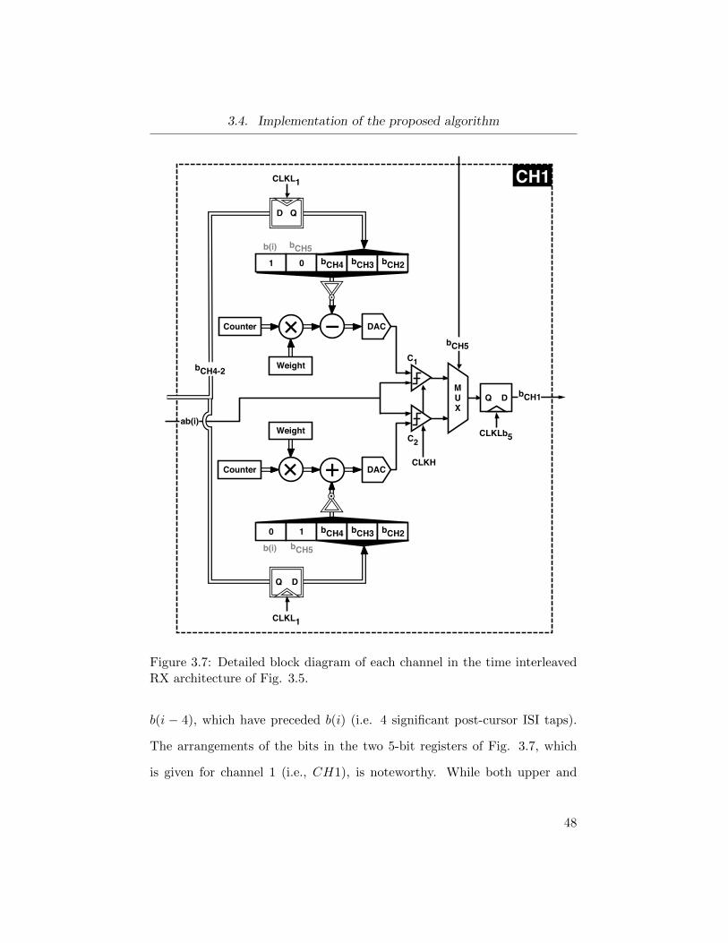
3.4. Implementation of the proposed algorithm
C1Weight
× DACCounter
bCH5b(i)
1 0 bCH4 bCH3 bCH2
−
Weight
× DACCounter
bCH5b(i)
0 1 bCH4 bCH3 bCH2
+C2
MUX
Q D
CLKLb5
bCH1
ab(i)
bCH5
CH1
CLKH
D Q
CLKL1
Q D
CLKL1
bCH4-2
Figure 3.7: Detailed block diagram of each channel in the time interleavedRX architecture of Fig. 3.5.
b(i − 4), which have preceded b(i) (i.e. 4 significant post-cursor ISI taps).
The arrangements of the bits in the two 5-bit registers of Fig. 3.7, which
is given for channel 1 (i.e., CH1), is noteworthy. While both upper and
48

3.4. Implementation of the proposed algorithm
CLKL5 (T/H5)
CLKL1 (T/H1)
CLKL2 (T/H2)
CLKLb4
CLKLb3
CLKLb5
CLKLb1
CLKL4 (T/H4)
CLKL3 (T/H3)
CLKLb2
CLKH
first SAR sample in CH1
last SAR sample in CH1
Figure 3.8: Timing diagram of the five time-interleaved channels.
49
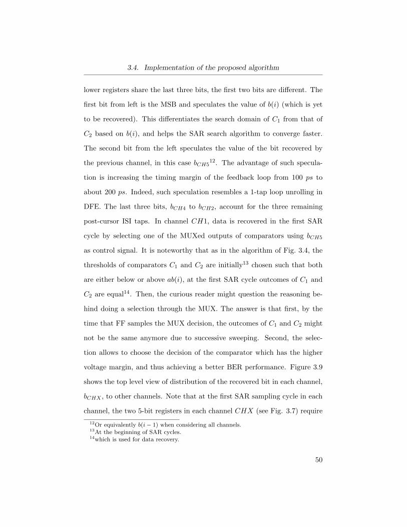
3.4. Implementation of the proposed algorithm
lower registers share the last three bits, the first two bits are different. The
first bit from left is the MSB and speculates the value of b(i) (which is yet
to be recovered). This differentiates the search domain of C1 from that of
C2 based on b(i), and helps the SAR search algorithm to converge faster.
The second bit from the left speculates the value of the bit recovered by
the previous channel, in this case bCH512. The advantage of such specula-
tion is increasing the timing margin of the feedback loop from 100 ps to
about 200 ps. Indeed, such speculation resembles a 1-tap loop unrolling in
DFE. The last three bits, bCH4 to bCH2, account for the three remaining
post-cursor ISI taps. In channel CH1, data is recovered in the first SAR
cycle by selecting one of the MUXed outputs of comparators using bCH5
as control signal. It is noteworthy that as in the algorithm of Fig. 3.4, the
thresholds of comparators C1 and C2 are initially13 chosen such that both
are either below or above ab(i), at the first SAR cycle outcomes of C1 and
C2 are equal14. Then, the curious reader might question the reasoning be-
hind doing a selection through the MUX. The answer is that first, by the
time that FF samples the MUX decision, the outcomes of C1 and C2 might
not be the same anymore due to successive sweeping. Second, the selec-
tion allows to choose the decision of the comparator which has the higher
voltage margin, and thus achieving a better BER performance. Figure 3.9
shows the top level view of distribution of the recovered bit in each channel,
bCHX , to other channels. Note that at the first SAR sampling cycle in each
channel, the two 5-bit registers in each channel CHX (see Fig. 3.7) require
12Or equivalently b(i− 1) when considering all channels.13At the beginning of SAR cycles.14which is used for data recovery.
50
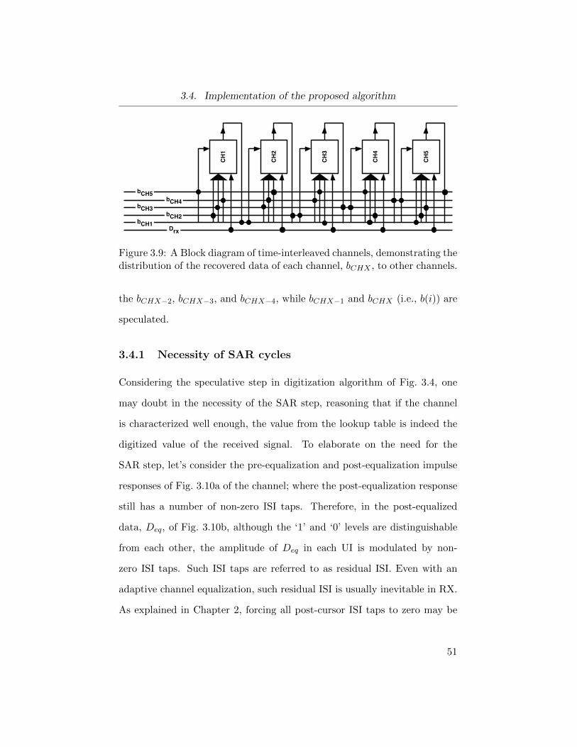
3.4. Implementation of the proposed algorithm
CH1
CH2
CH3
CH5
CH4
DrxbCH1
bCH2bCH3
bCH4bCH5
Figure 3.9: A Block diagram of time-interleaved channels, demonstrating thedistribution of the recovered data of each channel, bCHX , to other channels.
the bCHX−2, bCHX−3, and bCHX−4, while bCHX−1 and bCHX (i.e., b(i)) are
speculated.
3.4.1 Necessity of SAR cycles
Considering the speculative step in digitization algorithm of Fig. 3.4, one
may doubt in the necessity of the SAR step, reasoning that if the channel
is characterized well enough, the value from the lookup table is indeed the
digitized value of the received signal. To elaborate on the need for the
SAR step, let’s consider the pre-equalization and post-equalization impulse
responses of Fig. 3.10a of the channel; where the post-equalization response
still has a number of non-zero ISI taps. Therefore, in the post-equalized
data, Deq, of Fig. 3.10b, although the ‘1’ and ‘0’ levels are distinguishable
from each other, the amplitude of Deq in each UI is modulated by non-
zero ISI taps. Such ISI taps are referred to as residual ISI. Even with an
adaptive channel equalization, such residual ISI is usually inevitable in RX.
As explained in Chapter 2, forcing all post-cursor ISI taps to zero may be
51

3.4. Implementation of the proposed algorithm
h(↑)ch
h-1 h0 h2h1h-2 h3 h5h4
cursor
pre-equalisation ISI
residual ISI
(a)
0 125 250 375 500 6250.2
0.3
0.4
0.5
0.6
0.7
0.8
0.9
1
Rec
eive
d da
ta w
ith IS
I (V)
Time (ps)
residual ISI
(b)
Figure 3.10: Residual ISI in channel impulse response after the speculativedigitization step (a), and the effect of residual ISI in changing data levels(b).
52

3.5. Power/resolution trade-off in ADC and DAC
very power inefficient, or impossible15.
If the distortion in Deq is not captured at baud-rate, it can mislead the
CR algorithm and result in data dependent wandering around the optimal
locking point (i.e., where the maximum vertical eye-opening occurs). In
contrast, if the CR algorithm receives a precise digital representation of Deq
in each UI, it would be able to effectively track data dependent jitter (DDJ).
3.5 Power/resolution trade-off in ADC and DAC
In the proposed ADC, although the number of comparators remain con-
stant as the resolution increases, the resolution of the DAC should increase
accordingly. Therefore, at the first glance, it may seem that the power
consumption of the DAC offsets the power savings of the proposed ADC,
resulting in an overall power consumption comparable to that of a full-flash
architecture. However, a closer look at the elements of the high speed com-
parator and DAC reveals that power-consumption/resolution trade-off in
high speed ADCs is substantially more aggressive than in DACs operating
at comparable speeds. Our comparators are similar to that in [49] having
a preamplifier, two CML latches, and a CML-to-CMOS stage; all of which
drawing static current. On the other hand, if we neglect the typically low
power consumption of the digital logic, the price that we pay to increase the
resolution in a current-steering DAC is confined to that of a differential pair
with a tail current source [51]. It is important to mention that while all of
the CML blocks inside the comparator are constantly drawing static cur-
15Due to the self loading of the equalizer taps.
53

3.6. Measurement results and comparison
rent, the current sources inside the DAC can be completely switched on/off
based on the value of the digital code, further decreasing DAC’s power con-
sumption at the price of a slightly compromised conversion speed. With
the proposed ADC structure, we are pushing the power toll of increased
resolution towards the digital logic (low power consumption) and DAC (fair
power consumption), as opposed to the power-hungry comparators of flash
ADC.
3.6 Measurement results and comparison
As a proof-of-concept, an RX chip incorporating a 4-tap SASDFE is designed
and fabricated in a 65-nm CMOS technology. Figure 6.5a shows the chip
layout that occupies 1.242 × 1.239 mm (excluding the pads). To enable
digitization of the sampled signal, and facilitate a baud-rate clock-recovery
algorithm, 5 channels of SASDFE are time-interleaved at the RX front-
end. This allows for 5 SAR digitization cycles to adjust the speculated
level of the distorted received bit and find the digitized signal value. Each
channel runs at 10 GS/s which considering the 5 SAR cycles yields an overall
digitization and data recovery speed of 2 GS/s and 2 Gb/s, respectively. The
5 parallel channels used in this prototype provide a total data recovery speed
of 10 Gb/s. Figure 3.11b shows the measured eye diagram of the full rate
recovered data. The eye edges are rounded due to the bandwidth limitation
of measurement instrument. The circuit achieves a BER of better than
10−12 in response to a 27 − 1 pseudorandom binary sequence (PRBS) from
a channel with 19 dB loss at 5 GHz, while consuming overall power of 263
54

3.6. Measurement results and comparison
mW (all 5 channels collectively) from a 1 V supply. Table 3.1 compares the
characteristics and performance metrics of this work with recently published
ADC-based receivers. It can be seen that the proposed RX has a better16
power efficiency FoM compared to those of [27, 40–42, 52]. Additionally, the
systematically reduced comparator count in this work results in a smaller
die area for RX, compared to [41, 42, 52].
16A lower number for power efficiency FoM is considered to be better.
55

3.6. Measurement results and comparison
1239µmA
B
C D E
1242µm
B
(a)
(b)
Figure 3.11: The die micrograph of the prototype implemented in 65-nmCMOS (a); where the blocks A, B, C, D, and E are variable gain ampli-fier, clock phase generation, comparator array, DAC array, and DSP core,respectively. The measured eye diagram of the recovered 10 Gb/s data (b).
56
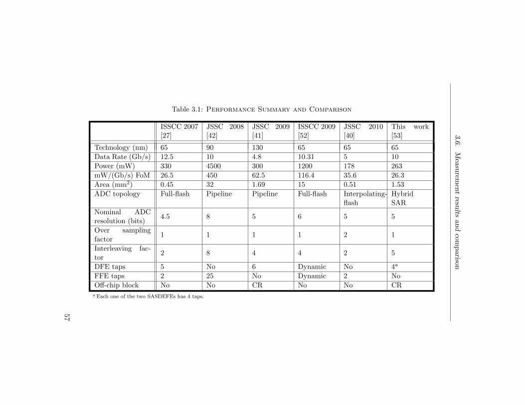
3.6.
Mea
surem
ent
results
and
comp
arison
Table 3.1: Performance Summary and Comparison
ISSCC 2007[27]
JSSC 2008[42]
JSSC 2009[41]
ISSCC 2009[52]
JSSC 2010[40]
This work[53]
Technology (nm) 65 90 130 65 65 65
Data Rate (Gb/s) 12.5 10 4.8 10.31 5 10
Power (mW) 330 4500 300 1200 178 263
mW/(Gb/s) FoM 26.5 450 62.5 116.4 35.6 26.3
Area (mm2) 0.45 32 1.69 15 0.51 1.53
ADC topology Full-flash Pipeline Pipeline Full-flash Interpolating-flash
HybridSAR
Nominal ADCresolution (bits)
4.5 8 5 6 5 5
Over samplingfactor
1 1 1 1 2 1
Interleaving fac-tor
2 8 4 4 2 5
DFE taps 5 No 6 Dynamic No 4a
FFE taps 2 25 No Dynamic 2 No
Off-chip block No No CR No No CRa Each one of the two SASDEFEs has 4 taps.
57

3.7. Chapter summary
3.7 Chapter summary
This chapter
Drx
RTCTLE
ADC DSP-based CDR Drec
CLKrec
Clock phase generation
AD
C-b
ased
RX
DSP-based DFE
Figure 3.12: Graphical illustration of ADC and DFE blocks addressed inthis Chapter, and their interaction with other RX blocks.
In this Chapter, a low-power architecture for high-speed ADC-based
wireline RX is presented. As illustrated in Fig. 3.12, we seek the power re-
duction goal through system-level enhancements of the digitization front-end
and DFE, similar to the SASDFE proposed in Chapter 2. As an alternative
to the power-hungry flash ADCs, a custom digitization algorithm is devel-
oped which utilizes the channel low-pass characteristic in order to speculate
the digitized value of the sampled signal and achieve a fast converging SAR
ADC. The hybrid speculative/SAR digitization algorithm allows to reach
a digitization speed of 2 GS/s per channel. Additional power savings are
achieved by obviating the need for the multi-stage buffers preceding the
ADC, and by embedding the data recovery and DFE functions within the
ADC algorithm. The timing margin of the DFE feedback loop is improved
by means of 1-tap loop unrolling, and the 5-way time-interleaved implemen-
tation of RX.
58

Chapter 4
Quadrature clock generation
in RX
Due to the orthogonality of quadrature clock phases, ΦI and ΦQ, they are
used at the front-end of “wireless” receivers to decode the data that has
been encoded in the phase of received signal. A simple form of such decod-
ing can be done through mixing two copies of the received data, which are
provided by a splitter, one with ΦI and the other with ΦQ. Two well known
modulation schemes that utilize phase encoding are quadrature phase shift
keying (QPSK), and quadrature amplitude modulation (QAM); where in
the former the data is merely encoded in phase of signal, whereas in the
latter data has been encoded in both phase and amplitude of signal. The
other potential use of quadrature phases in wireless RX is image rejection
in low-IF receivers [54].
In“wireline” systems, however, it is most common to encode the data in the
amplitude of transmitted signal as in binary or pulse amplitude modulation
(PAM) signaling. While in its conventional form, wireline RX may not need
quadrature clock phases, as discussed in Chapter 5, we utilize ΦI and ΦQ
for data phase shifting, and frequency doubling at CDR front-end.
59
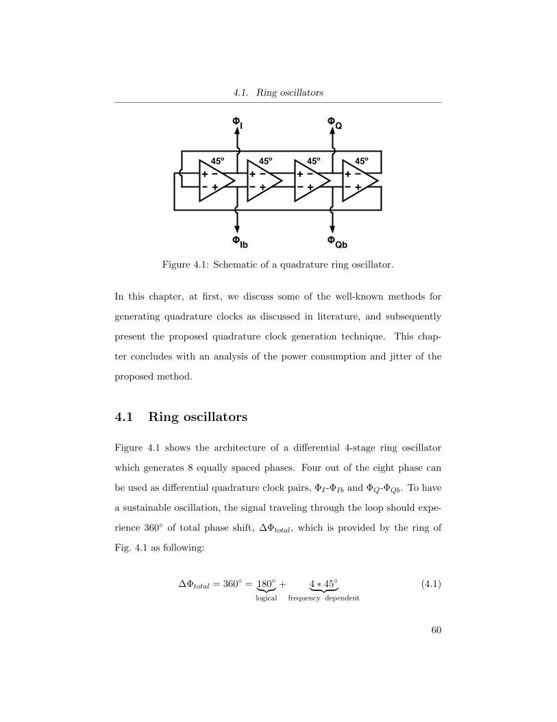
4.1. Ring oscillators
++
++
++
++
45º 45º 45º 45º
ΦIb ΦQb
ΦI ΦQ
Figure 4.1: Schematic of a quadrature ring oscillator.
In this chapter, at first, we discuss some of the well-known methods for
generating quadrature clocks as discussed in literature, and subsequently
present the proposed quadrature clock generation technique. This chap-
ter concludes with an analysis of the power consumption and jitter of the
proposed method.
4.1 Ring oscillators
Figure 4.1 shows the architecture of a differential 4-stage ring oscillator
which generates 8 equally spaced phases. Four out of the eight phase can
be used as differential quadrature clock pairs, ΦI -ΦIb and ΦQ-ΦQb. To have
a sustainable oscillation, the signal traveling through the loop should expe-
rience 360 of total phase shift, ∆Φtotal, which is provided by the ring of
Fig. 4.1 as following:
∆Φtotal = 360 = 180︸︷︷︸logical
+ 4 ∗ 45︸ ︷︷ ︸frequency dependent
(4.1)
60

4.1. Ring oscillators
The logical and frequency dependent phase shifts are provided by the cross-
connection in the feedback loop, and the phase shift of the inverter at the
frequency of the clock (f0), respectively.
The curious reader may wonder, if only 90 separated phases are required
and not the additional 45 phases, why the ring oscillator of Fig. 4.1 employs
4×45 scheme for frequency dependent delay and not 2×90 ? Specifically,
this question is legitimate as in first glance the 2 × 90 may provide less
phase jitter as employs half the number of noisy active elements in the
ring. Although such reasoning is partially true, it should be noted that a
stand alone inverter without an explicit load capacitance17, CL, may have a
smaller propagation delay compared to the desired propagation delay, tp,inv,
as given by
tp,inv = 90 =1
4× 1
f0(4.2)
Thus, compared to the 4×45 scheme, the 2×90 requires a larger CL. While
2×90 scheme offers less active elements, from a power consumption stand-
point, it may not provide an overall power saving as a larger capacitance
should be driven by each inverter. Also, a higher tp,inv usually translates to
a higher time constant in the output of each inverter, which aggravates the
effect of clock jitter. The 4× 45 configuration provides sharper clock edges
compares to the 2× 90 configuration.
17CL is not explicitly shown in Fig. 4.1.
61

4.2. LC oscillators
4.2 LC oscillators
4.2.1 Differential LC oscillators
Varactor
VCOtune
ΦIbΦI
(a)
Oscillator tank CL Rp
Active circuit(-Rp)
(b)
Figure 4.2: Schematic of an LC VCO (a), and canceling the parasitic resis-tance of inductor, Rp, in LC tank using an active element (b).
Figure 4.2a shows a typical architecture for an LC voltage controlled
oscillator, VCO, in which both NMOS and PMOS cross coupled pairs are
used to re-use the current and provide a higher negative resistance −Rp [55].
Figure 4.2b illustrates the fundamental of oscillation in the tank formed by
the inductor, L, capacitor, C, parallel resistance of inductor, Rp, and the
62

4.3. Phase noise and power trade-off
actively generated negative resistance −Rp. As Rp and −Rp cancel each
other, VCO should provide a sustainable oscillation at frequency f0 given
by
f0 =1
2π ×√L× C
(4.3)
unlike the ring oscillator which oscillates based on delay generation in feed-
back loop, the LC oscillator oscillates due to exchange of energy between
magnetic and electric fields.
4.2.2 Quadrature LC oscillators
Two LC tanks can be injection locked (coupled) to each other to generate
Quadrature phases. Figures 4.3a and 4.3b show two possible forms of in-
jection locking, where the former illustrates current-mode injection locking
using transistors, and the latter utilizes magnetic coupling between the two
tanks. Coupling through active devices (Fig. 4.3a) degrades the phase noise
of the overall quadrature oscillator due to the thermal and flicker noise of
coupling devices [56]. While magnetic coupling (Fig. 4.3b) provides a better
phase noise performance, the large area required by the coupling transformer
makes it an inferior design choice.
4.3 Phase noise and power trade-off
Each of the discussed clocking methods are subject to a trade-off among
area, power, and phase noise. In this section, we discuss such trade-off in
63
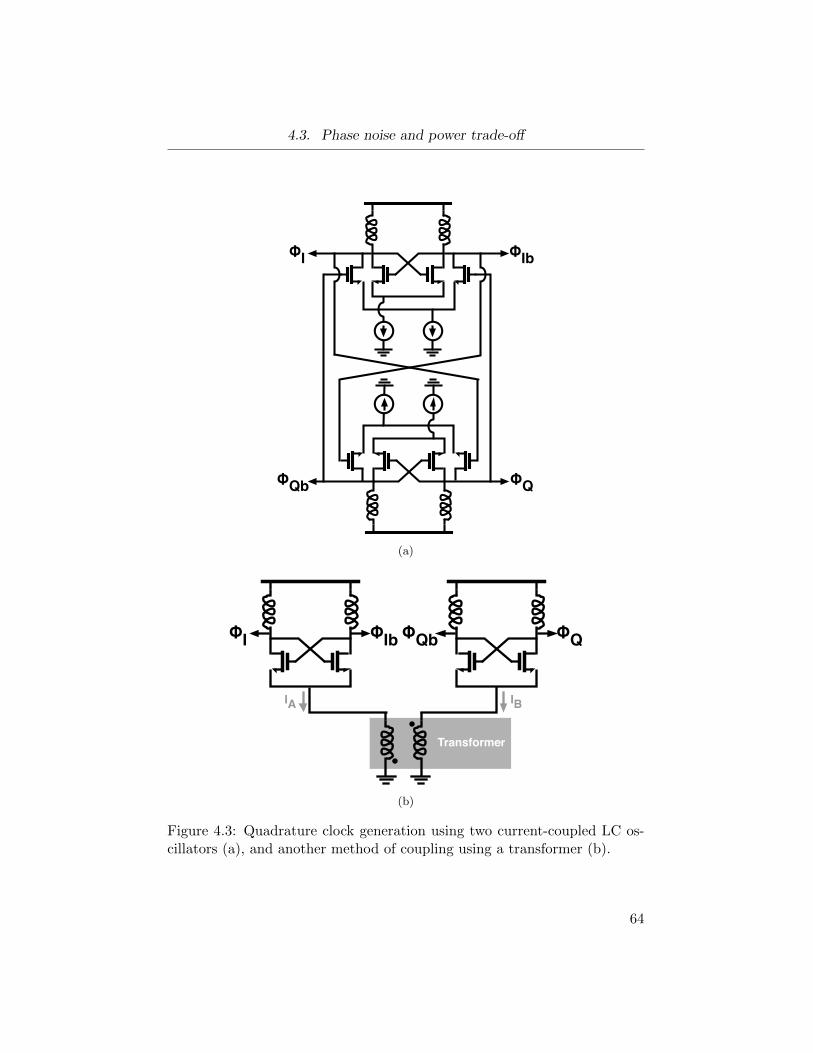
4.3. Phase noise and power trade-off
ΦI
ΦQb ΦQ
ΦIb
(a)
IB
Transformer
IA
ΦI ΦIb ΦQb ΦQ
(b)
Figure 4.3: Quadrature clock generation using two current-coupled LC os-cillators (a), and another method of coupling using a transformer (b).
64

4.3. Phase noise and power trade-off
LC tank VCO, ring VCO, and the proposed injection-locked QPG clocking
method.
4.3.1 Phase noise in LC VCO
Considering the simplified LC tank of Fig. 4.2b, the phase noise, Llc(∆ω),
of the LC VCO at frequency offset ∆ω is given by the following equation
[55]
Llc(∆ω) = 2kT
(3
8γ + 1
)(Rpvsw2
2
)(ω0
2Q∆ω
)2
(4.4)
where ω0 is the main oscillation frequency, and vsw,lc is the differential peak
swing which can be written as
vsw,lc =
(4
π
)(RpIlc
2
)=
2IlcRpπ
(4.5)
Hence, considering that
Rp = Q× L× ω0 (4.6)
we can re-write Eq. 4.4 as
Llc(∆ω) = π2kT
(3
8γ + 1
)(ω0
4LQ3Ilc2∆ω2
)(4.7)
65

4.3. Phase noise and power trade-off
4.3.2 Phase noise of ring oscillator
The first source of phase noise in a ring oscillator is the uncorrelated noise
of input devices in each inverter, that modulate the inverter delay and result
in phase noise. The second source of phase noise in ring oscillators is the 1f
(flicker) noise of tail current source in each inverter. As the current through
tail current sources are mirrors of a golden reference current, these noise
sources are correlated. The latter noise source results in significant phase
noise in ring oscillators and is inversely proportional to the tail current,
Iinv, in each inverter; hence, trading-off with the power consumption. For
the phase noise of a ring oscillator we can write
Lring(∆ω) =
(2kT
Iinv ln 2
)(7γ
4v∗+
1
vsw,ring
)( ω0
∆ω
)2(4.8)
where vsw,ring is the peak differential swing per stage, and v∗ ∝ (vgs − vth).
4.3.3 L(∆ω)-power-area trade-off in ring and LC oscillators
While a ring oscillator occupies an area equal to a fraction of smallest on
chip inductor, its phase noise is considerably higher than a well-designed LC
oscillator [55].
To investigate the phase noise/power trade-off between ring and LC oscilla-
tors, we set Llc(∆ω) of Eq. 4.7 equal to Llc(∆ω) of Eq. 4.8, and find the
relationship between the tail currents as following
IinvIlc≈ 8×Q2 × VDD
v∗(4.9)
66

4.4. Proposed quadrature clock generator
while for the total current in an N stage ring oscillator we can write
Iring = N × Iinv (4.10)
This reveals a steep trade-off between phase noise and power in ring oscilla-
tors as compared to the considerably more relaxed trade-off in LC oscillators.
Therefore, based on Eqs. 4.9 and 4.10, a 4-stage ring oscillator (that pro-
vides quadrature phases) should approximately dissipate 1000× the power
of an LC oscillator which has a tank Q of 2.5.
4.4 Proposed quadrature clock generator
LC VCO
Quadrature clock generator
!CLK
CLKb
ΦIΦQΦIbΦQb
Figure 4.4: Quadrature clock generation using coupling a differential VCOto the quadrature phase generation block.
In this work, quadrature clock phases are generated using injection lock-
ing of a delay ring to a differential LC VCO. Figure 4.4 shows how the
quadrature clock generator (QCG) block is injection locked through a transcon-
ductance stage to the relatively low-jitter clock phases, CLK and CLKb,
generated by a differential LC VCO.
Figure 4.5 illustrates the implementation of injection locking (coupling) in
67

4.4. Proposed quadrature clock generator
current domain. the coupling factor, α, is set by
α =IcplIss
(4.11)
where Icpl and Iss are the coupling current provided by the transconduc-
tance stage, and the tail current of the current mode logic (CML) inverters
of the QCG block.
Figure 4.6 shows the block diagram of the QCG block, which com-
DXBDXA
VIN VINb
VOUT
IcplIss
VOUTbCLKb CLK
Figure 4.5: Unilateral coupling through current injection into the QPS ring.
prises two cascaded sub-blocks, namely, quadrature phase splitter (QPS)
and quadrature phase corrector (QPC). Figures 4.8a and 4.8b show the de-
tailed structure of QPS and QPC, respectively. These sub-blocks are com-
posed of several inverters whose function is noted in the legend shown in
Fig. 4.7a. As shown in Fig. 4.7b, the single-ended inverters are used in pairs
and each pair of two such inverters form a differential current-mode logic
(CML) inverter. These inverters are used for three purposes: generate delay,
logically invert the signal, and act as buffer. The inverters used for logical
68
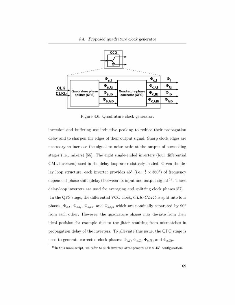
4.4. Proposed quadrature clock generator
Quadrature phase splitter (QPS)
Q
IQCG
Φs,IΦs,QΦs,IbΦs,Qb
Φc,IΦc,QΦc,IbΦc,Qb
Quadrature phase corrector (QPC)
ΦIΦQΦIbΦQb
CLKCLKb
Figure 4.6: Quadrature clock generator.
inversion and buffering use inductive peaking to reduce their propagation
delay and to sharpen the edges of their output signal. Sharp clock edges are
necessary to increase the signal to noise ratio at the output of succeeding
stages (i.e., mixers) [55]. The eight single-ended inverters (four differential
CML inverters) used in the delay loop are resistively loaded. Given the de-
lay loop structure, each inverter provides 45 (i.e., 18 × 360) of frequency
dependent phase shift (delay) between its input and output signal 18. These
delay-loop inverters are used for averaging and splitting clock phases [57].
In the QPS stage, the differential VCO clock, CLK-CLKb is split into four
phases, Φs,I , Φs,Q, Φs,Ib, and Φs,Qb which are nominally separated by 90
from each other. However, the quadrature phases may deviate from their
ideal position for example due to the jitter resulting from mismatches in
propagation delay of the inverters. To alleviate this issue, the QPC stage is
used to generate corrected clock phases: Φc,I , Φc,Q, Φc,Ib, and Φc,Qb.
18In this manuscript, we refer to such inverter arrangement as 8 × 45 configuration.
69
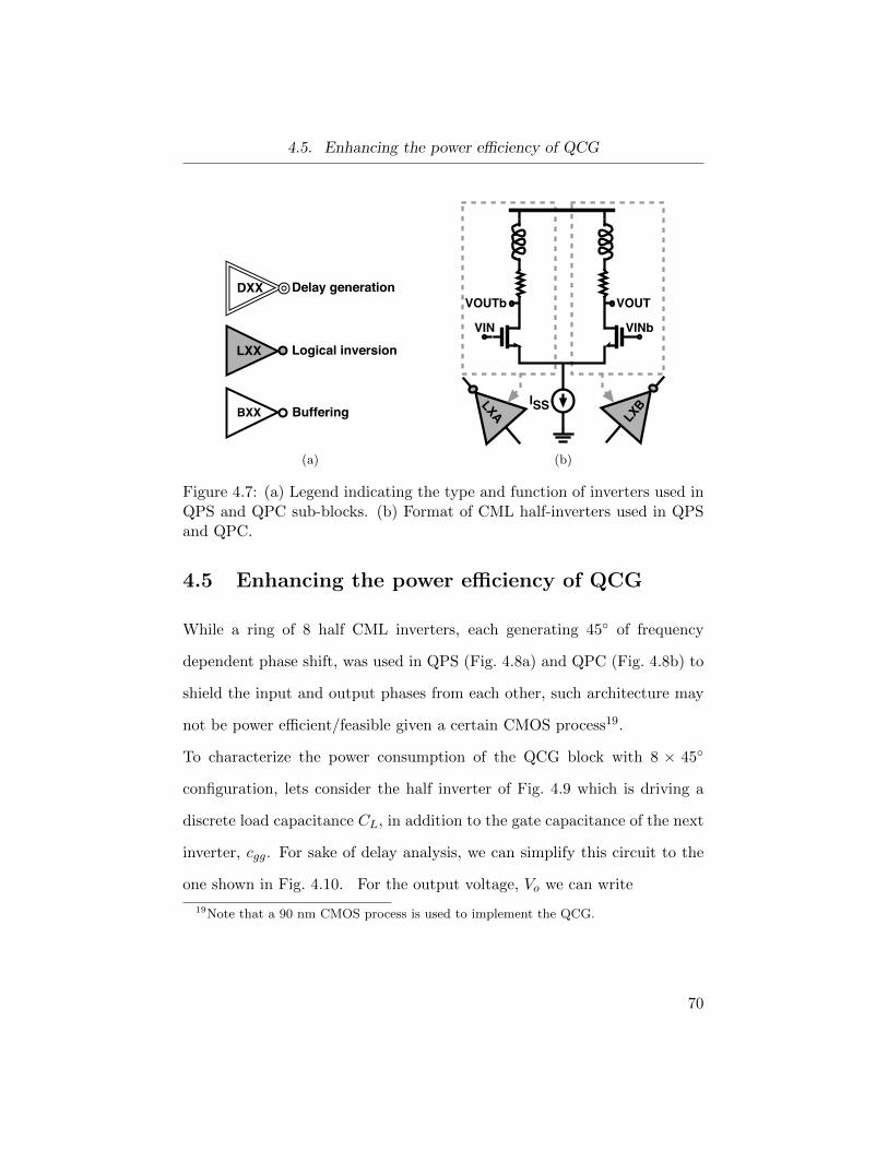
4.5. Enhancing the power efficiency of QCG
DXX
LXX
BXX
Delay generation
Logical inversion
Buffering
(a)
ISS
LXBLXA
VIN VINb
VOUTVOUTb
(b)
Figure 4.7: (a) Legend indicating the type and function of inverters used inQPS and QPC sub-blocks. (b) Format of CML half-inverters used in QPSand QPC.
4.5 Enhancing the power efficiency of QCG
While a ring of 8 half CML inverters, each generating 45 of frequency
dependent phase shift, was used in QPS (Fig. 4.8a) and QPC (Fig. 4.8b) to
shield the input and output phases from each other, such architecture may
not be power efficient/feasible given a certain CMOS process19.
To characterize the power consumption of the QCG block with 8 × 45
configuration, lets consider the half inverter of Fig. 4.9 which is driving a
discrete load capacitance CL, in addition to the gate capacitance of the next
inverter, cgg. For sake of delay analysis, we can simplify this circuit to the
one shown in Fig. 4.10. For the output voltage, Vo we can write
19Note that a 90 nm CMOS process is used to implement the QCG.
70
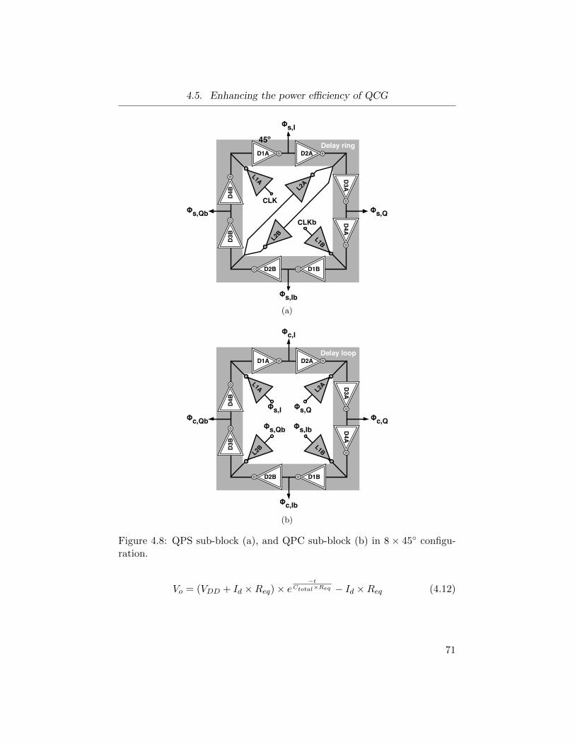
4.5. Enhancing the power efficiency of QCG
Delay ringD1A D2A
D3B
D4B
D1BD2B
D3A
D4A
Φs,QΦs,Qb
Φs,I
Φs,Ib
45º
L1A
CLK
L1B
CLKb
L2A
L2B
(a)
Delay loopD1A D2A
L2BD3B
D4B
L1A L2A
L1B
D1BD2B
D3A
D4A
Φs,IbΦs,Qb
Φs,QΦs,IΦc,QΦc,Qb
Φc,I
Φc,Ib
(b)
Figure 4.8: QPS sub-block (a), and QPC sub-block (b) in 8 × 45 configu-ration.
Vo = (VDD + Id ×Req)× e−t
Ctotal×Req − Id ×Req (4.12)
71

4.5. Enhancing the power efficiency of QCG
VibCL
RL
VoId,sat
Iss
Figure 4.9: AC representation of the half CML inverter.
Device in saturation
CtotalRLId,sat 1/(!Id,sat)
Figure 4.10: Simplified model used for delay calculation.
where λ is the channel length modulation factor. For Req we have
Req = (RL||1
λId) (4.13)
and considering the self loading capacitance of M1, cdd, the total capacitance
at node Vo, Ctotal, is given by
Ctotal = cgg + cdd + CL (4.14)
72
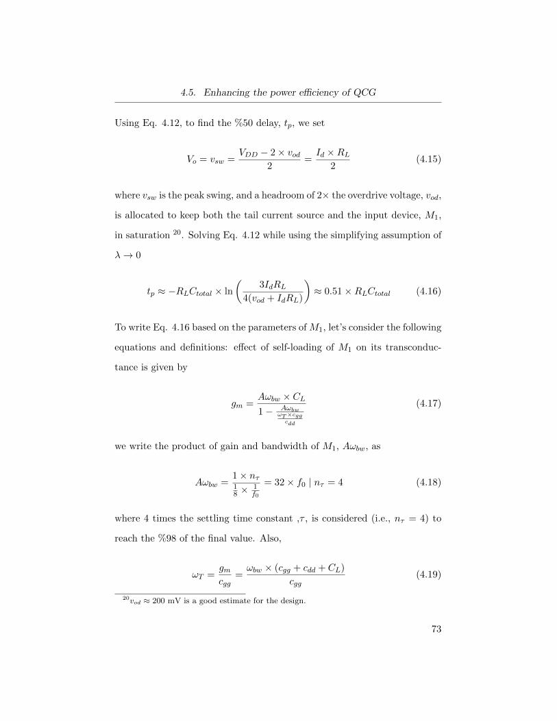
4.5. Enhancing the power efficiency of QCG
Using Eq. 4.12, to find the %50 delay, tp, we set
Vo = vsw =VDD − 2× vod
2=Id ×RL
2(4.15)
where vsw is the peak swing, and a headroom of 2× the overdrive voltage, vod,
is allocated to keep both the tail current source and the input device, M1,
in saturation 20. Solving Eq. 4.12 while using the simplifying assumption of
λ→ 0
tp ≈ −RLCtotal × ln
(3IdRL
4(vod + IdRL)
)≈ 0.51×RLCtotal (4.16)
To write Eq. 4.16 based on the parameters of M1, let’s consider the following
equations and definitions: effect of self-loading of M1 on its transconduc-
tance is given by
gm =Aωbw × CL1− Aωbw
ωT×cggcdd
(4.17)
we write the product of gain and bandwidth of M1, Aωbw, as
Aωbw =1× nτ18 ×
1f0
= 32× f0 | nτ = 4 (4.18)
where 4 times the settling time constant ,τ , is considered (i.e., nτ = 4) to
reach the %98 of the final value. Also,
ωT =gmcgg
=ωbw × (cgg + cdd + CL)
cgg(4.19)
20vod ≈ 200 mV is a good estimate for the design.
73
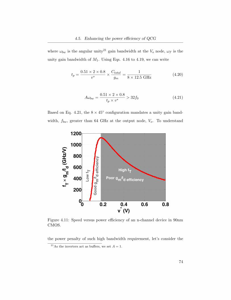
4.5. Enhancing the power efficiency of QCG
where ωbw is the angular unity21 gain bandwidth at the Vo node, ωT is the
unity gain bandwidth of M1. Using Eqs. 4.16 to 4.19, we can write
tp =0.51× 2× 0.8
v∗× Ctotal
gm=
1
8× 12.5 GHz(4.20)
Aωbw =0.51× 2× 0.8
tp × v∗> 32f0 (4.21)
Based on Eq. 4.21, the 8 × 45 configuration mandates a unity gain band-
width, fbw, greater than 64 GHz at the output node, Vo. To understand
0 0.2 0.4 0.6 0.80
200
400
600
800
1000
1200
v* (V)
f T × g
m/I d (G
Hz/
V)
High fTPoor gm/Id efficiencyLo
w f T
Goo
d g m
/I d ef
ficie
ncy
Figure 4.11: Speed versus power efficiency of an n-channel device in 90nmCMOS.
the power penalty of such high bandwidth requirement, let’s consider the
21As the inverters act as buffers, we set A = 1.
74

4.5. Enhancing the power efficiency of QCG
intrinsic speed versus power efficiency of an N-channel device. Figure 4.11
shows the fT×gmId
FoM for an NMOS in 90-nm technology. The peak of FoM
graph, where device offers the best trade-off between speed and power ef-
ficiency, occurs at v∗ ≈ 200 mV. For v∗ > 0.2 V the device provides good
speed but poor power efficiency, while v∗ < 0.2 V results in good power
efficiency at the price of lower speed (lower fT ). An fbw value compara-
ble to maximum fT of device (i.e., fbw = fT,max) can push the operation
point of the device towards the right region, in which the device quickly
becomes power-inefficient, and requires large vod. Therefore, to allow for a
lower required fbw at node Vo, we can modify the architecture of the QCG
from a 8× 45 configuration to the 8× 90 configuration shown in Fig. 4.12.
Figures 4.12a and 4.12b show the modified architectures for QPS and QPC
sub-blocks in which the delay ring inverters have a frequency dependent
phase shift of 90 at the clock frequency, f0. This reduces the required fbw
at node V0 of ring inverters to ≈ 32.5 GHz. Equation 4.21 sets an upper
limit for v∗, while as shown in Fig. 4.13, the lower limit is partially set by the
sensitivity of tp to variation in v∗. Figure 4.14 shows the power consumption
of a single inverter in each of the configurations versus v∗. The exponen-
tial increase in the power consumption of the inverter for the lower values
of v∗ is noteworthy. Specially, Eq. 2.10 suggests that given a certain gm,
the power consumption is proportional to v∗, while Fig. 4.14 suggests and
inverse relationship. Such inverse relationship for lower values of v∗ (e.g.,
v∗ < 0.2 V) can be explained by considering the self loading effect of the
transistor. As the fT of the device degrades in this region and gets closer
to fbw, the power penalty due to driving the self loading capacitance of the
75
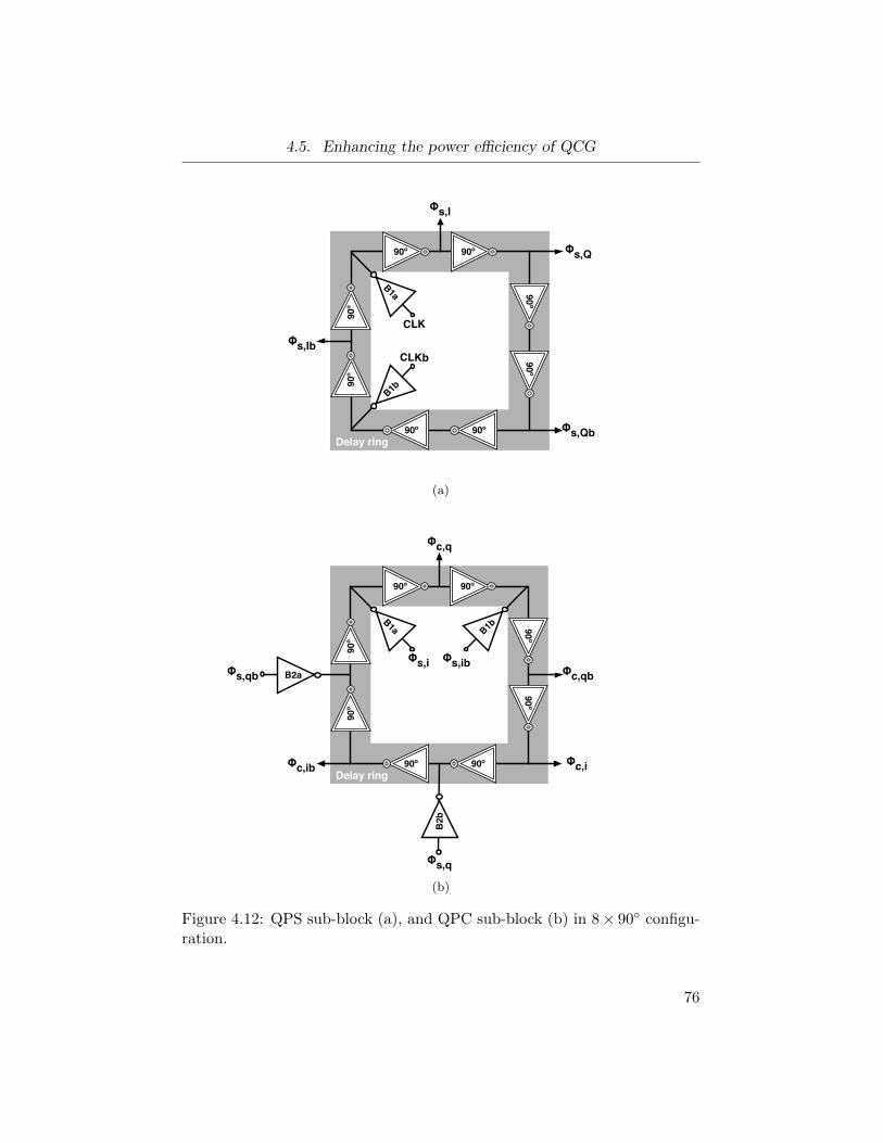
4.5. Enhancing the power efficiency of QCG
90º 90º
Φs,I
90º
90º
CLK
CLKb
90º90º
90º90º
B1a
B1b
Delay ring
Φs,Q
Φs,Qb
Φs,Ib
(a)
90º 90º
Φc,q
90º
90º
90º90º
90º90º
B1a B1b
Delay ringΦc,i
Φs,i Φs,ibB2aΦs,qb Φc,qb
B2b
Φs,q
Φc,ib
(b)
Figure 4.12: QPS sub-block (a), and QPC sub-block (b) in 8× 90 configu-ration.
76

4.5. Enhancing the power efficiency of QCG
device (cdd) becomes significant. Therefore, power consumption is the other
key factor in determining the lower limit of v∗.
0.15 0.2 0.25 0.3
5
10
15
20
25
v* (V)
Del
ay (t
p, ps)
8×45°, CL=0.4×cgg
8×90°, CL=2×cgg
Figure 4.13: Delay of inverter as a function of v∗.
Note that for each graph in Figs. 4.13 and 4.14, a certain amount of CL
has been used to set the desired delay (i.e., for f0= 12.5 GHz, inverter delays
should be equal to 10 ps and 20 ps for 8 × 45 and 8 × 90, respectively).
As Figure 4.15 suggests, one remedy is to coarsely set v∗ ≈ 0.2 V, and
then fine tune the value of tp using CL. Fig. 4.15 reveals another interesting
result; while operating in the left hand region of Fig. 4.11, increasing the
delay through adding CL, versus decreasing v∗ can significantly reduce the
power consumption of each delay stage (inverter).
77
4.5. Enhancing the power efficiency of QCG
0.12 0.14 0.16 0.18 0.20
0.5
1
1.5
v* (V)
Pow
er (m
W)
8×45°, CL=0.4×cgg
8×90°, CL=2×cgg
Figure 4.14: Power consumption of the inverter as a function of v∗.
0 5 10 151
1.5
2
2.5
3
CL (×cgg)
Pow
er (m
W)
8×90° config
Figure 4.15: Effect of using a discrete load capacitance, CL, on power con-sumption per inverter stage. Plotted for a constant value of tp.
78

4.6. Jitter in QCG block
4.6 Jitter in QCG block
To analyze the jitter22 performance of the proposed QCG, let’s consider the
half inverter of Fig. 4.9. The AC voltage at node Vo is given by
Vo = vsw sin(ω0t+ φ1) + n(t) (4.22)
where ω0 = 2π×12.5 GHz23, φ1 is the arbitrary phase of the waveform, and
n(t) is a term representing the contribution of all noise sources (i.e., noise of
passives and actives). Hence, the variance of absolute time jitter, στ2, and
variance of phase jitter, σφ2, are given [58] as
σφ2 = ω0
2 × στ 2 =σn
2
vsw2(4.23)
Based on Eq. 4.23, to reduce the jitter contribution of each inverter, we
should either increase vsw, or decrease σn2. We discuss the trade-offs asso-
ciated with each of these options.
4.6.1 Maximizing voltage swing
While connecting the cascaded inverters in the DC-coupled format shown
in Fig. 4.16 provides the lowest CL at the timing critical node, Vo, such ap-
proach limits the maximum vsw achievable at Vo. In a 8×90 configuration,
the voltages at nodes Vo and V bi can be written with respect to each other
22Jitter and phase noise are used interchangeably in this manuscript, where the formerrefers to quality of clock edges in time domain, whereas thee latter refers to purity of clockspectrum in frequency domain.
23The VCO clock, CLK, is considered to have a frequency of 12.5 GHz.
79
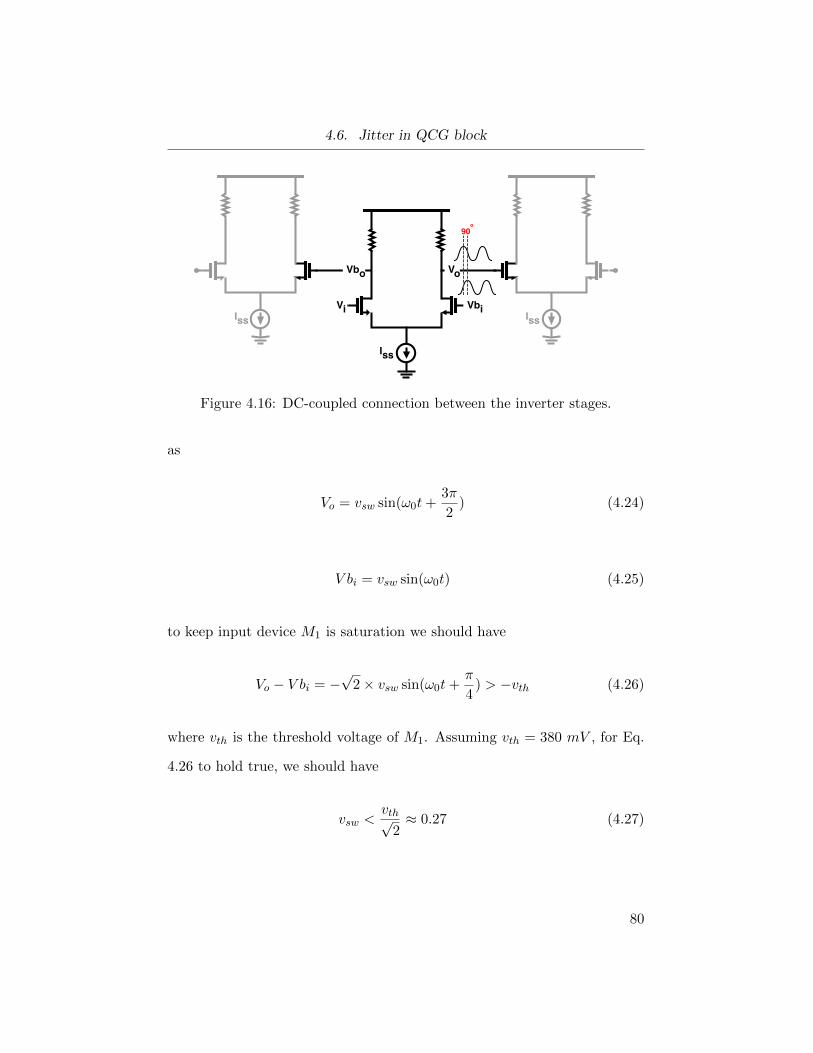
4.6. Jitter in QCG block
Iss
IssIss
Vo
90º
Vbo
Vbi Vi
Figure 4.16: DC-coupled connection between the inverter stages.
as
Vo = vsw sin(ω0t+3π
2) (4.24)
V bi = vsw sin(ω0t) (4.25)
to keep input device M1 is saturation we should have
Vo − V bi = −√
2× vsw sin(ω0t+π
4) > −vth (4.26)
where vth is the threshold voltage of M1. Assuming vth = 380 mV , for Eq.
4.26 to hold true, we should have
vsw <vth√
2≈ 0.27 (4.27)
80

4.6. Jitter in QCG block
which indeed limits the maximum swing achievable 24 at node Vo. Note that
the 8× 45 configuration offers a higher upper-bound for DC-coupled swing
as we have
vsw <vth√
2−√
2≈ 0.5 (4.28)
which indicates that the 8 × 45 configuration allows for the desired vsw
of 0.4 V. Therefore, to choose either 8 × 45 or 8 × 90 configuration, we
should consider parameters such as f0, fT×gmId
of devices (Fig. 4.11), vsw,
sensitivity of tp to v∗ variations (Fig. 4.13), and power efficiency of inverters
(Fig. 4.14) given the values chosen for v∗ and CL.
The AC-coupled version of the circuit shown in Fig. 4.16 deserves some
attention. Figure 4.17 illustrates AC-coupled biasing of inverter stages
through a “T” connection. The voltage at the gate of device M3 is at-
tenuated through the capacitive voltage division of the coupling capacitor
Ccop with the gate capacitance of M3, cgg, for which we can write
Vg3 =Vo × CcopCcop + cgg
(4.29)
Hence we choose Ccop ≈ 10 × cgg. Also, we set the cutoff frequency of the
high-pass filter formed by Ccop and R1 well below f0. Hence, we have
1
R1 × Ccop f0 (4.30)
24Note that without considering the biasing of succeeding and preceding stages, themaximum achievable vsw, in each CML inverter stage is ≈ 0.4 V (i.e., VDD−2v∗
2) in a
90-nm technology with 1.2 V supply.
81

4.6. Jitter in QCG block
Vib
Ibias
Vo
CcopRL
Cdecap
R1
M1M2
M3 M4
Figure 4.17: AC-coupled connection between the inverter stages.
A decoupling capacitor, Cdecap, is used at the gate of the tail current to
avoid the modulation of Id through high frequency deterministic and random
noise. As the value of Cdecap need not precisely match a specific value25, it
is realized through forming metal-oxide-metal (MoM) caps using the metal
layers that are used to fill the chip.
25The larger the value of Cdecap, the lower the bandwidth at gate of tail current sourcewould be, hence Cdecap would be capable of filtering noise up-to lower frequencies.
82

4.6. Jitter in QCG block
4.6.2 Noise of actives and passives in inverter stage
The mean square noise voltage, vn2, at the Vo node in the differential inverter
of Fig. 4.9 is given by
vn2(f) = 2× (RL||ro1)2 ×
Kgm12
CoxWLf︸ ︷︷ ︸1f
noise
+8KTgm1
3+
4KT
RL︸ ︷︷ ︸thermal noise
(4.31)
note that the factor 2× in Eq. 4.31 is due to the fact that the noise voltage
power of a differential stage is twice that of a single-ended stage [34]. To
find the phase noise spectral density, Sφ(∆f), we can write
Sφ(∆f) = 2Linv(∆f) =vn2(f)
vsw2=
4× vn2(f)
(Id ×RL)2 (4.32)
where Linv(∆f) is the single-sided phase noise spectrum of Vo around f0.
From Eq. 4.32, we can calculate the variance of the period jitter, σ2pj,inv,
as
σ2pj,inv =
(1
πf0
)2 ∫ f02
0sin2
(π ×∆f
f0
)Sφ(∆f) d∆f (4.33)
While due to the 1f term in Eq. 4.31 an explicit answer for the integral
of Eq. 4.33 does not exist, by ignoring the contribution of flicker noise to
vn2(f) we can write
σ2pj,inv =
(2
f0
)×(RL||ro1πIdRL
)2
×(
8KTgm1
3+
4KT
RL
)(4.34)
83
4.6. Jitter in QCG block
Using the maximum allowable peak swing of 2v∗, and based on Eqs. 4.15,
and 2.10, we simplify Eq. 4.34 as
σ2pj,inv =
(1
Id
)×(
38KT
3π2v∗f0
)︸ ︷︷ ︸≈ 2×10⁻³⁰
(4.35)
where we have assumed RL ro1. Using Eq. 4.35 we can get to the RMS
period jitter, Jpj,inv, by
Jpj,inv (fs) =√σ2
pj ≈√
2
Id(4.36)
Eq. 4.36 shows that Jpj,inv trades-off with 1√Id
. Thus revealing the steep
power penalty in achieving a low-jitter design for a single inverter cell. As the
noise in each of the 8 inverters in the rings of QPS and QPC are uncorrelated,
for the total period jitter variance of the rings, σ2pj,rqp, we can write
σ2pj,rqp = 8× σ2
pj,inv (4.37)
Likewise, for the RMS period jitter contribution of QPS and QPC rings,
Jpj,rqp, we have
Jpj,rqp (fs) = 2√
2× Jpj,inv =4√Id
(4.38)
Equation 4.38 demonstrates the fundamental amount of jitter that would
be added to the clock phases by the QPS and QPC rings.
84

4.7. Chapter summary
4.7 Chapter summary
DrxDSP-based
DFE
RTCTLE
ADC DSP-based CDR Drec
CLKrec
Drx Analog DFE
RTCTLE
Analog CDR Drec
CLKrec
Clock phase generation
Clock phase generation
AD
C-b
ased
RX
Ana
log
RX
This chapter
This chapter
Figure 4.18: Graphical illustration of quadrature clock generation blockintroduced in this Chapter, and its interaction with other RX blocks.
An open loop method for generating quadrature clock phases from the
differential clock provided by a VCO is presented. The proposed technique is
utilized in the analog and digital CDRs presented in Chapters 5 and 6. The
orthogonality of CLKI and CLKQ makes quadrature clock phases an inte-
gral part of most modern CDRs. Figure 4.18 shows the interaction of QCG
with other blocks in analog and digital CDRs. While in a phase interpola-
tor based CDR (i.e., dual-loop CDR), QCG clock phases are feed-forwarded
to the interpolation/DLL loop, in a PLL based CDR (i.e., the single-loop
CDRs presented in Chapter 5), the QCG is located in the main feedback
85
4.7. Chapter summary
loop. When quadrature clock phases are needed at various locations in a
large system-on-a-chip (SoC), the QCG block allows to locally generate the
phases and avoid the challenges and distortions associated with routing the
phases over long distances. Finally, this Chapter analyzes the phase noise
performance of the QCG. Such analysis helps to determine the optimum
number of QPC blocks which follow the QPS block.
86
Chapter 5
Analog CDR in high-speed
links
Clock and data recovery (CDR) systems play a vital role in high-speed
wireline links to achieve power and hardware efficient data transmission at
bit error rates (BERs) better than 10−12. In this Chapter, we investigate
analog CDR architectures, and propose a PLL-based CDR suited for multi-
Gb/s speeds, which exploits a mixer as phase detector (PD).
5.1 Line codes in serial links
While there are numerous line coding methods discussed in literature [59],
this manuscript focuses on non-return to zero (NRZ) signaling. Such line
coding has universally become the method of choice for transmitting binary
data across wireline channels. Let’s consider the waveforms in Fig. 5.1,
which represent return to zero (RZ) and NRZ lines codes along with a baud-
rate clock. For a data pattern of consecutive ‘1’s and ‘0’s, the number of
transitions in an RZ code are equal to that of baud-rate clock and twice
the transitions in NRZ code. Therefore, unlike the RZ code, NRZ does
not have a clock component in its spectrum. Due to the presence of a clock
87
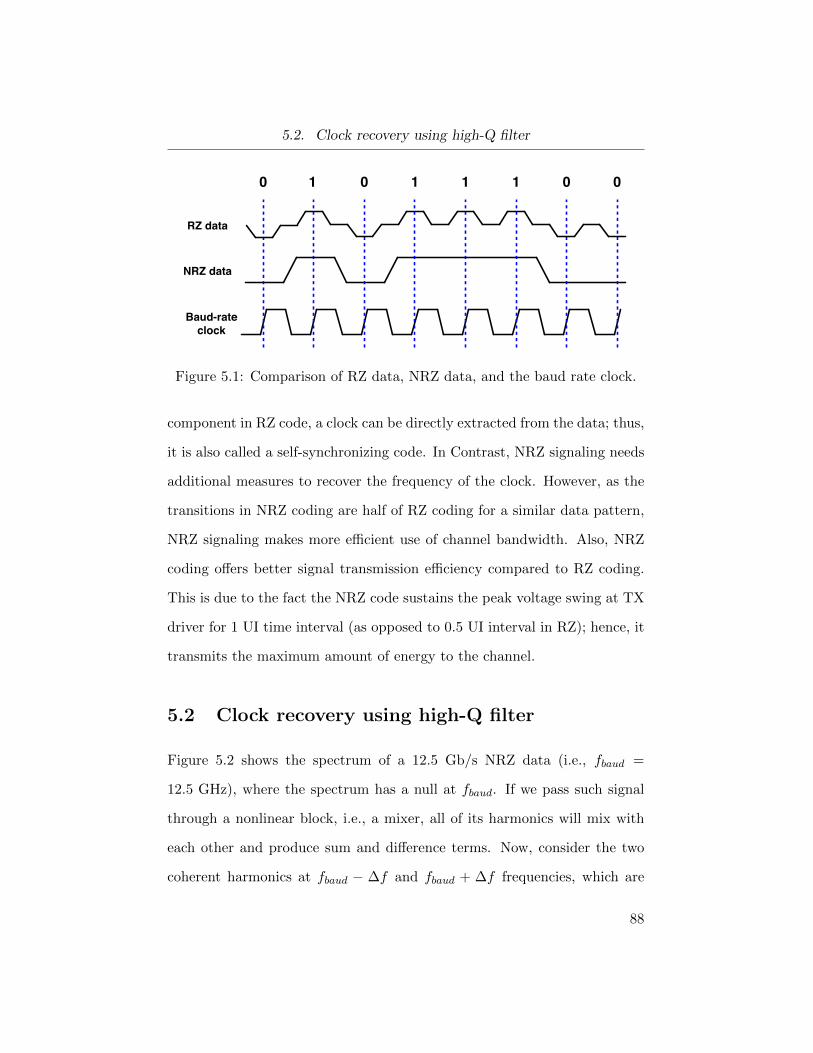
5.2. Clock recovery using high-Q filter
0 1 0 1 1 1 0 0
NRZ data
Baud-rate clock
RZ data
Figure 5.1: Comparison of RZ data, NRZ data, and the baud rate clock.
component in RZ code, a clock can be directly extracted from the data; thus,
it is also called a self-synchronizing code. In Contrast, NRZ signaling needs
additional measures to recover the frequency of the clock. However, as the
transitions in NRZ coding are half of RZ coding for a similar data pattern,
NRZ signaling makes more efficient use of channel bandwidth. Also, NRZ
coding offers better signal transmission efficiency compared to RZ coding.
This is due to the fact the NRZ code sustains the peak voltage swing at TX
driver for 1 UI time interval (as opposed to 0.5 UI interval in RZ); hence, it
transmits the maximum amount of energy to the channel.
5.2 Clock recovery using high-Q filter
Figure 5.2 shows the spectrum of a 12.5 Gb/s NRZ data (i.e., fbaud =
12.5 GHz), where the spectrum has a null at fbaud. If we pass such signal
through a nonlinear block, i.e., a mixer, all of its harmonics will mix with
each other and produce sum and difference terms. Now, consider the two
coherent harmonics at fbaud − ∆f and fbaud + ∆f frequencies, which are
88

5.2. Clock recovery using high-Q filter
0 6.25 12.5 18.75 25 31.25−120
−110
−100
−90
−80
−70
−60
−50
−40
Frequency (GHz)
Pow
er (d
B)
fbaud-Δf fbaud+Δf
Figure 5.2: The harmonics around fbaud in the spectrum of NRZ data, whichare used to extract the baud-rate clock.
annotated as two impulses in Fig. 5.2. Each of these harmonics can be
represented by a sine wave in time domain as following
hrm1 = A1 × sin(2π(fbaud −∆f) + φ1) (5.1)
hrm2 = A2 × sin(2π(fbaud + ∆f) + φ2) (5.2)
If we pass the sine waves of Eqs. 5.1 and 5.2 through a non-linear element,
we would get a DC term and another term at 2fbaud. In the same manner,
the coherent terms around fbaud2 and 2fbaud will produce tones at fbaud, and
4fbaud, respectively. By filtering tones at frequencies higher or lower than
fbaud, we would be able to recover a clock whose frequency is equal to the
baud rate of data, and has an arbitrary phase. The system shown in Fig. 5.3
89
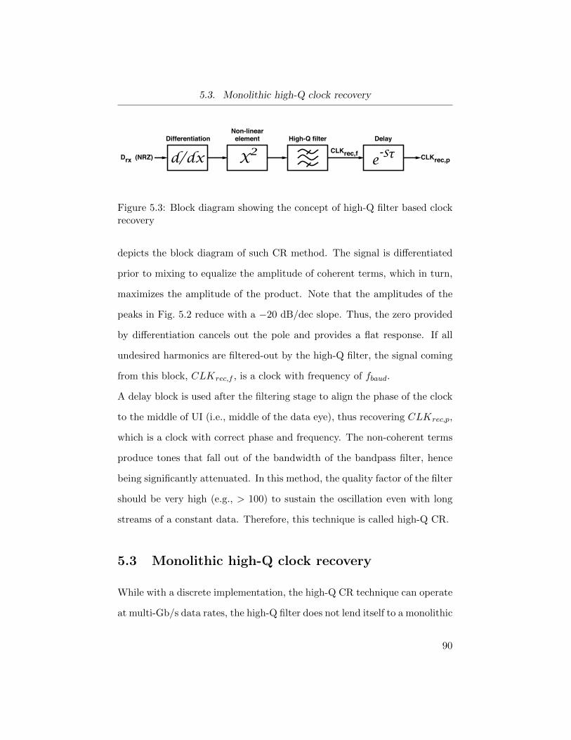
5.3. Monolithic high-Q clock recovery
d/dx
Non-linear elementDifferentiation High-Q filter
CLKrec,f CLKrec,pX2Delay
e-s!Drx (NRZ)
Figure 5.3: Block diagram showing the concept of high-Q filter based clockrecovery
depicts the block diagram of such CR method. The signal is differentiated
prior to mixing to equalize the amplitude of coherent terms, which in turn,
maximizes the amplitude of the product. Note that the amplitudes of the
peaks in Fig. 5.2 reduce with a −20 dB/dec slope. Thus, the zero provided
by differentiation cancels out the pole and provides a flat response. If all
undesired harmonics are filtered-out by the high-Q filter, the signal coming
from this block, CLKrec,f , is a clock with frequency of fbaud.
A delay block is used after the filtering stage to align the phase of the clock
to the middle of UI (i.e., middle of the data eye), thus recovering CLKrec,p,
which is a clock with correct phase and frequency. The non-coherent terms
produce tones that fall out of the bandwidth of the bandpass filter, hence
being significantly attenuated. In this method, the quality factor of the filter
should be very high (e.g., > 100) to sustain the oscillation even with long
streams of a constant data. Therefore, this technique is called high-Q CR.
5.3 Monolithic high-Q clock recovery
While with a discrete implementation, the high-Q CR technique can operate
at multi-Gb/s data rates, the high-Q filter does not lend itself to a monolithic
90
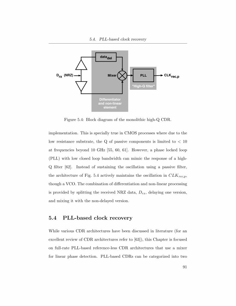
5.4. PLL-based clock recovery
"High-Q filter"
Mixer
datadel
PLL CLKrec,p
Differentiator and non-linear
element
Drx (NRZ)
Figure 5.4: Block diagram of the monolithic high-Q CDR.
implementation. This is specially true in CMOS processes where due to the
low resistance substrate, the Q of passive components is limited to < 10
at frequencies beyond 10 GHz [55, 60, 61]. However, a phase locked loop
(PLL) with low closed loop bandwidth can mimic the response of a high-
Q filter [62]. Instead of sustaining the oscillation using a passive filter,
the architecture of Fig. 5.4 actively maintains the oscillation in CLKrec,p,
though a VCO. The combination of differentiation and non-linear processing
is provided by splitting the received NRZ data, Drx, delaying one version,
and mixing it with the non-delayed version.
5.4 PLL-based clock recovery
While various CDR architectures have been discussed in literature (for an
excellent review of CDR architectures refer to [63]), this Chapter is focused
on full-rate PLL-based reference-less CDR architectures that use a mixer
for linear phase detection. PLL-based CDRs can be categorized into two
91
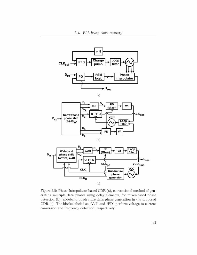
5.4. PLL-based clock recovery
PFD Charge pump
÷ N
Loop filter
FSM logic
Phase interpolator
Drx PD
CLKref
Drec
(a)
V/I
FD V/I
Drx Drec Narrowband
phase shift (!"@f0)
PD(Mixer)XOR
Dx
VCOLoop filter
Q FF D
DI
DQ
D3
D4
D5(b)
PD(Mixer)
Loop filter
Quadrature phase
generator
Q FF D
Wideband phase shift
(!"@f0 ± !f)
V/IXORDrx
Drec CLKpd VCOtune
Dx
VCO
DI
DQ
CLKI
CLKQ(c)
Figure 5.5: Phase-Interpolator-based CDR (a), conventional method of gen-erating multiple data phases using delay elements, for mixer-based phasedetection (b), wideband quadrature data phase generation in the proposedCDR (c). The blocks labeled as “V/I” and “FD” perform voltage-to-currentconversion and frequency detection, respectively.
92
5.4. PLL-based clock recovery
main groups: those that do not control V COtune, and those which adjust
the phase and frequency of the clock by tweaking V COtune. A good example
of the first group is phase-interpolator (PI) based CDR. Shown in Fig. 5.5a,
such CDR interpolates among the quadrature phases provided by VCO, to
adjust the phase of the PD clock. The frequency of the VCO is locked to
multiples of an external reference using a secondary PLL loop.
Figure 5.5b shows a generic block diagram of the second group of PLL-based
CDRs[64, 65], in which phase detection is performed using a mixer. A no-
table advantage of mixer-based phase detection is that unlike conventional
linear phase detection methods [66], it does not require pulse generation and
comparison for detection of the clock misalignment. Hence, mixer-based PDs
are a suitable candidate for phase detection at data rates beyond 10 Gb/s
[64]. In previous works, the various data phases required for equalization
and phase/frequency detection are generated either actively through the de-
lay of cascaded inverters [64, 65], or passively using emulated transmission
lines [5]. In these methods, the phase shift is typically frequency depen-
dent and thus the desired phase shift (e.g., 90) is only achieved at or in a
narrowband vicinity of a particular input frequency. In general, these con-
ventional phase-shifters have a narrowband response and they are typically
augmented by additional circuitry to adjust the phase shift. Note that the
received data, Drx, typically has a broadband spectrum; thus, the phase
shifter should provide the desired phase shift over a wide frequency range
which is a challenging task [55]. Additionally, if there is any variation be-
tween the nominal baud frequency, f0, (i.e., 12.5 GHz for 12.5 Gb/s data)
and the actual baud frequency, fbaud, for example due to process, supply
93

5.5. Frequency doubling for mixer-based PD
or temperature (PVT) variations, the CDR performance will be degraded
(e.g., additional jitter will be added to the data phases). In view of these
challenges of conventional phase shifters, which typically have a narrowband
response, we propose the architecture of Fig.5.5c. In this architecture, phase
shifting of the data is achieved by first generating quadrature clock phases,
CLKI and CLKQ, from the recovered clock; then, I/Q components of the
received data, DI and DQ, are generated by means of mixing Drx with
CLKI and CLKQ. The proposed architecture applies a modified form of
delay-based phase generation to the relatively narrowband recovered clock,
as opposed to directly applying it to the broadband data.
Prior to discussing the details of the top-level block diagram of Fig. 5.7,
first, we investigate the requirements and challenges of mixer-based phase
detection.
5.5 Frequency doubling for mixer-based PD
In the CDR system of Fig. 5.5c, if we directly mix Drx with CLKpd26, we
can write
Vpd = Drx⊗CLKpd =
α1α2
2[cos(
ωt
2+ θ) + cos(
3ωt
2+ θ)], ∆D = 1
α1α2 cos(ωt+ θ), ∆D = 0
(5.3)
where CLKpd = α1 cos(ωt + θ), Drx = α2 cos(ωt2 ), θ is the phase error in
clock with respect to data eye center, and ∆D is a binary (true/false) value
that indicates whether data has a transition (‘01’ or ‘10’) within 1 unit
26For simplicity, the equations are only written for single-ended signals instead of dif-ferential signals.
94
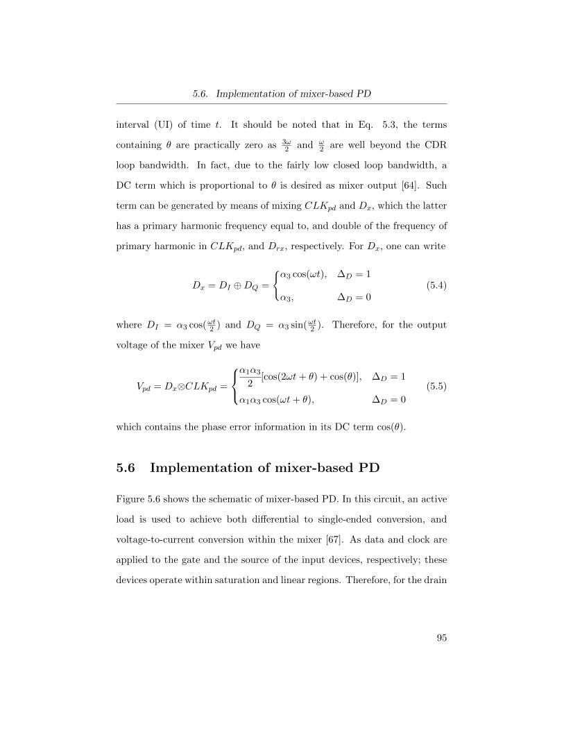
5.6. Implementation of mixer-based PD
interval (UI) of time t. It should be noted that in Eq. 5.3, the terms
containing θ are practically zero as 3ω2 and ω
2 are well beyond the CDR
loop bandwidth. In fact, due to the fairly low closed loop bandwidth, a
DC term which is proportional to θ is desired as mixer output [64]. Such
term can be generated by means of mixing CLKpd and Dx, which the latter
has a primary harmonic frequency equal to, and double of the frequency of
primary harmonic in CLKpd, and Drx, respectively. For Dx, one can write
Dx = DI ⊕DQ =
α3 cos(ωt), ∆D = 1
α3, ∆D = 0(5.4)
where DI = α3 cos(ωt2 ) and DQ = α3 sin(ωt2 ). Therefore, for the output
voltage of the mixer Vpd we have
Vpd = Dx⊗CLKpd =
α1α3
2[cos(2ωt+ θ) + cos(θ)], ∆D = 1
α1α3 cos(ωt+ θ), ∆D = 0
(5.5)
which contains the phase error information in its DC term cos(θ).
5.6 Implementation of mixer-based PD
Figure 5.6 shows the schematic of mixer-based PD. In this circuit, an active
load is used to achieve both differential to single-ended conversion, and
voltage-to-current conversion within the mixer [67]. As data and clock are
applied to the gate and the source of the input devices, respectively; these
devices operate within saturation and linear regions. Therefore, for the drain
95

5.6. Implementation of mixer-based PD
IpdId2
Id1Id2
DX DXb
CLKpdbCLKpd
Figure 5.6: Schematic of the mixer used as phase detector.
current of device Mn, we can write
Idn = β1(vgs,n − vth) + β2(vgs,n − vth)2 + β3(vgs,n − vth)3 (5.6)
where as an example, for device M1 we have vgs,1=Dx-CLKpd. In the mixer,
branch currents Id1 and Id2 add up at the output node and result in Ipd.
Based on Eqs. 5.5 and 5.6, Ipd can be analytically written as
Ipd = Id1 + Id2 (5.7)
∝
4α1α3β2[cos(4πfbaudt+ θ + Φopt) + cos(θ − Φopt)], ∆D = 1
8α1α3β2[cos(2πfbaudt+ θ)], ∆D = 0
where θ represents the phase error in CLKI with respect to the point in
Drx eye where the maximum vertical opening occurs, Φopt is a constant
term representing the optimal phase offset (explained in Section 5.9). As
the loop filter attenuates all components at 2ω and ω, for the phase detector
96

5.7. The proposed CDR architecture
Mixer (PD)
XOR Loop filterV/I
Calibrationphase
interpolator
I
QQuadrature clock
generator
Drx (12.5 Gb/s)
VCO (EWV1202YF)
Q FF D
12.5 GHz
CLKI (12.5 GHz)CLKQ (12.5 GHz)
Wideband phase shifter
CLKpd(12.5 GHz)
Drec
CPItune
Dx
2
Mixer (PS1)
Mixer (PS2)
DI
DQ
Figure 5.7: Detailed block diagram of the proposed CDR. In the proof-of-concept chip, the shaded blocks are off-chip.
characteristic, PDC, we can write
PDC ∝ cos(θ − Φopt). (5.8)
Equation 5.8 reveals two important properties of the proposed architecture:
First, among parameters β1, β2 and β3; only β2 is present in Ipd. Thus,
the phase error θ is measured while the devices operate in saturation. This
is, indeed, a desired result for high-speed operation. Second, while no data
transitions are present (∆D = 0), Ipd will be silent; hence, it is not per-
turbing the VCO control voltage. The latter is crucial for minimizing clock
jitter.
5.7 The proposed CDR architecture
Figure 5.7 shows the detailed block diagram of the proposed full-rate CDR
topology, which uses a mixer as a linear PD. The shaded blocks are not inte-
grated on the proof-of-concept prototype chip and are implemented off-chip.
97
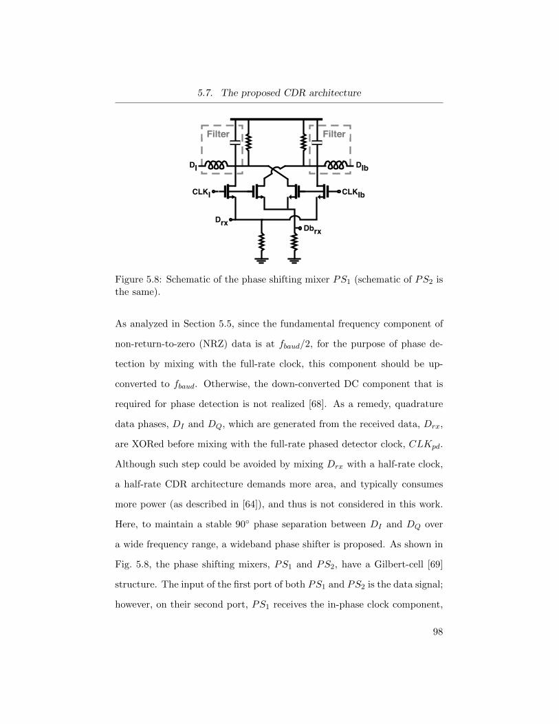
5.7. The proposed CDR architecture
Filter Filter
Drx Dbrx
CLKIbCLKI
DIbDI
Figure 5.8: Schematic of the phase shifting mixer PS1 (schematic of PS2 isthe same).
As analyzed in Section 5.5, since the fundamental frequency component of
non-return-to-zero (NRZ) data is at fbaud/2, for the purpose of phase de-
tection by mixing with the full-rate clock, this component should be up-
converted to fbaud. Otherwise, the down-converted DC component that is
required for phase detection is not realized [68]. As a remedy, quadrature
data phases, DI and DQ, which are generated from the received data, Drx,
are XORed before mixing with the full-rate phased detector clock, CLKpd.
Although such step could be avoided by mixing Drx with a half-rate clock,
a half-rate CDR architecture demands more area, and typically consumes
more power (as described in [64]), and thus is not considered in this work.
Here, to maintain a stable 90 phase separation between DI and DQ over
a wide frequency range, a wideband phase shifter is proposed. As shown in
Fig. 5.8, the phase shifting mixers, PS1 and PS2, have a Gilbert-cell [69]
structure. The input of the first port of both PS1 and PS2 is the data signal;
however, on their second port, PS1 receives the in-phase clock component,
98
5.7. The proposed CDR architecture
CLKI , while PS2 receives the quadrature clock component, CLKQ. As fun-
damental harmonics of Drx, CLKI , and CLKQ are at fbaud/2, fbaud, and
fbaud, respectively; DI and DQ are signals whose fundamental harmonics
are at fbaud/2 and are 90 separated in the time domain (or equivalently
14×fbaud ). As shown in Fig. 5.8, to avoid undesired higher frequency harmon-
ics to reach the XOR and PD, and being down-converted to a frequency
within the CDR loop bandwidth, second-order LC low-pass filters are used
at the output nodes of the differential mixer [55].
To improve clock edge alignment and data recovery, CLKpd and the CLKI -
CLKQ pair should maintain a certain constant phase offset, Φoff , relative
to each other. As explained in section 5.9, the value of Φoff depends on the
amount of channel loss, or equivalently the post-equalization residual ISI in
Drx. Therefore, a calibration phase interpolator (CPI) is used to provide
Φoff , by interpolating between CLKI and CLKQ. Note that unless the
channel is considerably time-variant, the CPI tuning signal, CPItune, needs
to be adjusted once, at the startup cycle of the CDR operation. On-chip
realization of a DSP-based calibration loop [70, 71] was beyond the scope of
this work; therefore, for the purpose of testing the prototype chip, CPItune
is manually set based on the loss of the channel used to transmit the data
to the chip.
To confirm the potential of such architecture in tracking moderate frequency
offsets without the help of a frequency detector, a single-loop topology is
used in the implementation of the proposed CDR. If a wider frequency
tracking range is required, the CDR architecture of Fig. 5.7 can be modified
by adding a second loop containing a frequency detection mechanism and
99
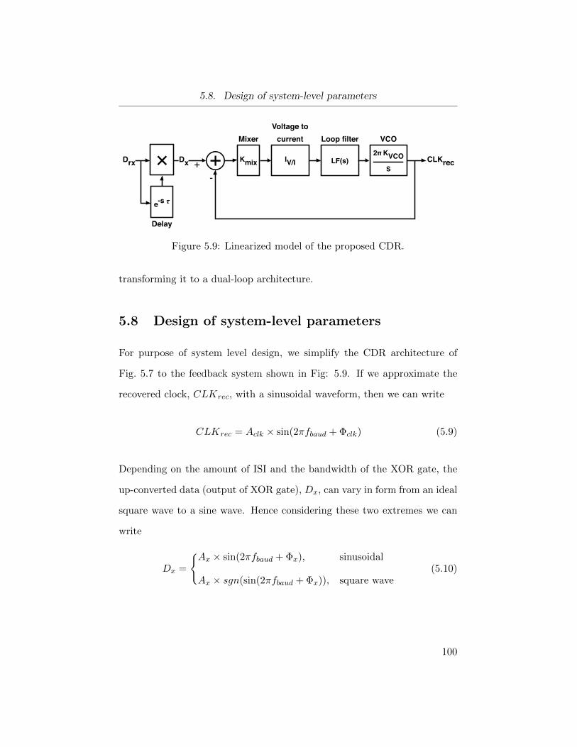
5.8. Design of system-level parameters
VCO2π KVCO
S
Loop filter
LF(s)IV/I
Voltage to current
Kmix
Mixer
+Dx +-
CLKrec×Drx
e-s !
Delay
Figure 5.9: Linearized model of the proposed CDR.
transforming it to a dual-loop architecture.
5.8 Design of system-level parameters
For purpose of system level design, we simplify the CDR architecture of
Fig. 5.7 to the feedback system shown in Fig: 5.9. If we approximate the
recovered clock, CLKrec, with a sinusoidal waveform, then we can write
CLKrec = Aclk × sin(2πfbaud + Φclk) (5.9)
Depending on the amount of ISI and the bandwidth of the XOR gate, the
up-converted data (output of XOR gate), Dx, can vary in form from an ideal
square wave to a sine wave. Hence considering these two extremes we can
write
Dx =
Ax × sin(2πfbaud + Φx), sinusoidal
Ax × sgn(sin(2πfbaud + Φx)), square wave(5.10)
100
5.8. Design of system-level parameters
where |Dx|, and Φx are the amplitude and phase of up-converted data at a
given time.
Kmix =
AxAclk
2, sinusoidal Dx
2AxAclkπ
, square wave Dx
(5.11)
For the open loop transfer function, OLTF (s), we can write
OLTF (s) =Dx(s)
CLKrec(s)=
2πKmix|Iv/i|KvcoLF (s)
s(5.12)
and the closed loop transfer function, CLTF (s), can be written as
CLTF (s) =OLTF (s)
1 +OLTF (s)(5.13)
5.8.1 Loop filter
There are two important design parameters associated with the loop filter of
an analog CDR (or PLL), namely type, and order. The type of a CDR loop
is regarded as the number of integrators in the OLTF (s). The minimum
type is ‘I’ as the VCO provides one integration, i.e. the ‘s’ in denominator
of Eq. 5.12. The order is referred to the roll-off factor in CLTF (s).
In this work, a type II architecture is utilized for the closed loop system
to achieve a high DC closed loop gain, which in turn results in consistent
steady state phase error. Additionally, having a second integration in the
loop filter in addition to the integration provided by VCO, allows to use the
entire tuning range of VCO. Therefore, the loop filter is designed as shown
in Fig. 5.10. The transfer function of the loop filter, LF (s) can be written
101

5.8. Design of system-level parameters
Loop filter
Iv/i VCOtune
C1 C2
R1
Figure 5.10: Type II, order 2 loop filter, as used in the proposed CDR.
as
LF (s) =V COtune(s)
Iv/i(s)=
1 + sR1C2
s(C1 + C2)(1 + sR1C∗)=Klf × (1 + s
2πfz)
s× (1 + s2πfp
)(5.14)
where C∗ and the gain of loop filter, Klf are given by
C∗ =C1C2
C1 + C2(5.15)
Klf =β
2πKvcoKmix|Iv/i|(5.16)
and for β, and fp we can write
β =2π2 × CDRbw ×QQ
CDRbw+ 1
fz− 1
Q×CDRbw
(5.17)
fp = CDRbw ×(
1
Q+
Q× fzQ× CDRbw − fz
)(5.18)
102
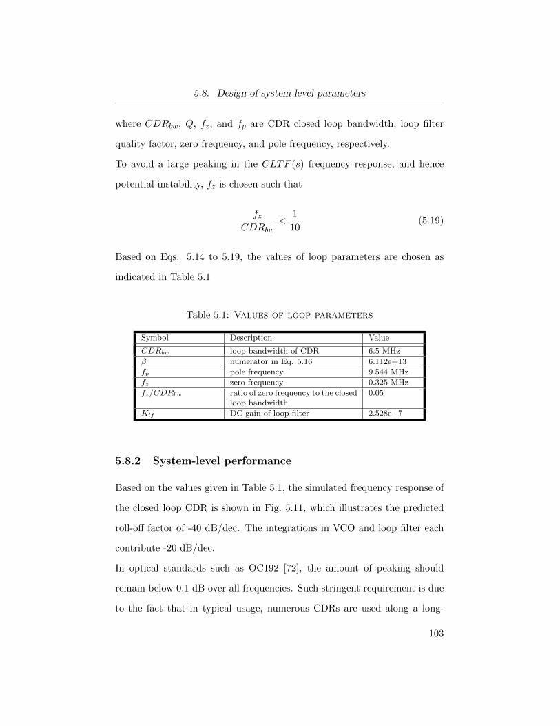
5.8. Design of system-level parameters
where CDRbw, Q, fz, and fp are CDR closed loop bandwidth, loop filter
quality factor, zero frequency, and pole frequency, respectively.
To avoid a large peaking in the CLTF (s) frequency response, and hence
potential instability, fz is chosen such that
fzCDRbw
<1
10(5.19)
Based on Eqs. 5.14 to 5.19, the values of loop parameters are chosen as
indicated in Table 5.1
Table 5.1: Values of loop parameters
Symbol Description Value
CDRbw loop bandwidth of CDR 6.5 MHz
β numerator in Eq. 5.16 6.112e+13
fp pole frequency 9.544 MHz
fz zero frequency 0.325 MHz
fz/CDRbw ratio of zero frequency to the closedloop bandwidth
0.05
Klf DC gain of loop filter 2.528e+7
5.8.2 System-level performance
Based on the values given in Table 5.1, the simulated frequency response of
the closed loop CDR is shown in Fig. 5.11, which illustrates the predicted
roll-off factor of -40 dB/dec. The integrations in VCO and loop filter each
contribute -20 dB/dec.
In optical standards such as OC192 [72], the amount of peaking should
remain below 0.1 dB over all frequencies. Such stringent requirement is due
to the fact that in typical usage, numerous CDRs are used along a long-
103

5.8. Design of system-level parameters
1M 10M 100M−70
−60
−50
−40
−30
−20
−10
0
10
Mag
nitu
de (d
B)
Frequency (Hz)
Figure 5.11: Frequency response of the closed loop CDR.
haul fiber channel to repeat the signal and avoid signal loss at the RX end
of channel. As the CDRs are cascaded, the peaking amounts add-up in
frequency domain, which can potentially make the overall system unstable.
Figure 5.12 reveals the step response of the CDR. The amount of overshoot
in the step response has a direct relationship with the value of fzCDRbw
. Figure
5.13 shows the response of CDR to an abrupt change in the data rate, DR, of
the received data. AsDR changes from the nominal value of 12.5 Gb/s to the
offset data rate of 12.6 Gb/s, the CDR demonstrates an unstable response
known as cycle slipping, during which gradually adjusts the VCO frequency.
While cycle slipping, the frequency of VCO is constantly changing in a
non-monotonic fashion. Therefore, during such period the CDR is prone
to making bit decision errors. The duration of cycle slip has an inverse
104

5.8. Design of system-level parameters
0 0.2 0.4 0.6 0.8 10
0.2
0.4
0.6
0.8
1
1.2
1.4
Am
plitu
de
Time (µs)
Figure 5.12: Step response of the CDR.
0 10 20 30 40 500.4
0.6
0.8
1
1.2
1.4
VCO
tune
Time (ms)
DR=12.6 Gb/s
DR=12.5 Gb/s
Figure 5.13: Frequency locking behavior of the CDR when the DR isswitched from 12.5 Gb/s to 12.6 Gb/s.
105

5.9. Calibration phase interpolator
relationship with CDRbw.
5.9 Calibration phase interpolator
Depending on the channel frequency response, the optimal position for sam-
pling the data (where maximum vertical eye opening occurs) can deviate
from the center of the unit interval [71]. Figure 5.14a shows normalized
PDC graphs for various values of channel loss. To obtain each PDC graph,
the CDR feedback path is opened and the phase of CLKpd is swept with re-
spect to phase of CLKI , while the sampling edge of CLKI is forced to align
with the optimal sampling point of Drx. As these PDC graphs are plotted
for the optimal sampling point, the vertical axis is labeled as PDCopt. Also,
the zero crossing of each PDC graph is denoted as Φopt. The horizontal axis
of Fig. 5.14a represents the phase offset between CLKpd and CLKI , Φoff .
It can be observed that within a π domain of Φoff values, for each PDC
graph, there is only one point27 for which we have Φoff = Φopt. Note that
the PD error signal at Φopt is zero, hence, it is the only point at which CDR
can sustain lock. For other values of Φoff such that Φoff 6= Φopt, the closed
loop CDR may still lock to a certain point of the Drx eye; however, such
point would be sub-optimal. If we plot Φopt versus different values of channel
loss, we would get the graph of Fig. 5.14b, which demonstrates that Φopt is
a strong function of the channel loss (or residual ISI in Drx), an undesired
result indeed. Therefore, using CPI block, we allow a degree of freedom in
CLKpd, through Φoff , to decouple it from CLKI (CLKQ). By adjusting
27The other point in the 2π domain flips the polarity of PDC in Eq. 5.8.
106

5.10. Performance of QCG block
CPItune, one can interpolate between CLKI and CLKQ to generate the
desired phase shift, Φoff = Φopt. For a constant BER, such calibration
technique allows for tolerating more residual ISI in Drx, and hence lower
power consumption in equalizer [53]. Note that in the conventional CDR
of Fig. 5.5b, although DI and DQ are decoupled from CLKpd, the integrity
of the 90 phase shift between DI and DQ still depends on the frequency
content of Drx, e.g., the magnitude of the harmonics in Drx; therefore, con-
ventional CDR of Fig. 5.5b is more sensitive to under/over equalization of
Drx.
5.10 Performance of QCG block
Figure. 5.15a shows the Monte Carlo simulations of RMS phase jitter of the
quadrature phases in cascaded inverters, QPS without QPC 28, and QPS
with QPC. The addition of the QPC sub-block enhances the quality of the
quadrature phases by reducing the RMS phase jitter due to deterministic
variations in the delay of inverters (e.g., due to mismatches in layout). How-
ever, cascading more than one quadrature phase correction stage (QPC) is
avoided due to area considerations, and the fact that the overall jitter in
clock phases will gradually become dominated by the random noise of the
inverters.
As QCG block is located in CDR’s feedback path, the quality of the gener-
ated clock phases directly affects the CDR performance in phase detection
and frequency tracking. In particular, in the presence of a frequency offset
28note that throughout this manuscript, the cascaded combination of QPS and QPCsub-blocks are called “quadrature phase generator” (QPG).
107

5.10. Performance of QCG block
ï
ï
Phase offset (+off, rad)
PDC op
t (nor
mal
ized
)G%ORVVG%ORVVG%ORVVG%ORVV
Linear regionΦopt
-3π/2 -π -π/2 π/20
(a)
1 100
20
40
60
80
100
120
Drx attenuation at Nyquist (dB)
Φop
t (°)
PDC∝−sin(θ−Φopt)PDC∝cos(θ−Φopt)PDC∝−cos(θ−Φopt)
90º phase shift
270º phase shift
(b)
Figure 5.14: Normalized PDCopt as a function of Φoff (a). Variation inΦopt due to various amounts of channel loss (b).
108

5.10. Performance of QCG block
−20 −10 0 10 200
5
10
15
∆ Inverter delay (%)
Pha
se ji
tter
(rm
s,
°)
Cascaded invertersQPS without QPCQPS with QPC
(a)
−15k−10k −5k 0 5k 10k 15k1.5
2
2.5
3
3.5
Frequency offset (ppm)
Jitte
r (σ
, de
gree
) ±10 kppm
(b)
Figure 5.15: Phase jitter in generated clock phases as a function of inverterdelay variation (a). Jitter performance of QCG versus offset from f0 (b).
109

5.11. Experimental results
between TX PLL and RX CDR, QCG should be able to provide low-jitter
phases over the part of VCO tuning range that falls within the operation
range of the CDR. Figure 5.15b shows the standard deviation of jitter in
outputs of QCG versus frequency offset from f0 (i.e., nominal fbaud). As can
be seen from the figure, the QCG block achieves a satisfactory performance
within ±10 kppm offset from f0 of 12.5 GHz. Note that this value sets
the upper limit for the frequency tracking range of the overall CDR. Fig-
ure 5.16 compares the power spectral density (PSD) of the signal Dx, when
DI and DQ are generated using the conventional narrowband phase shifting
method, and the proposed wideband phase shifting method. In respect to
the desired harmonic at 12.5 GHz, the PSD graphs of the conventional and
proposed phase shifting methods reveal jitters of 4 psrms and 2.32 psrms in
Dx, respectively.
5.11 Experimental results
The chip is designed and fabricated in a 90-nm CMOS technology. Figure
5.17 shows the die micrograph which occupies 0.98×0.84 mm2 excluding the
pads. As mentioned earlier, the chip integrates all the non-shaded blocks
shown in Fig. 5.7. The CDR’s loop bandwidth is set to about 6.5 MHz
through the external second-order type-II loop filter. In order to close
the CDR loop, an external VCO (Endwave EWV1202YF) is controlled by
filtered output of PD, to provide the recovered differential clock back to
the test-chip. The VCO provides ±0.25 GHz of symmetrical tuning range
around an f0 of 12.5 GHz. The free running phase noise of VCO is mea-
110
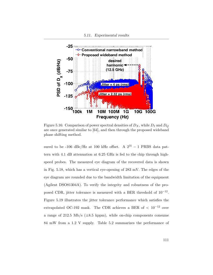
5.11. Experimental results
desired harmonic (12.5 GHz)
Jitter = 4 ps (rms)
Jitter = 2.32 ps (rms)
Figure 5.16: Comparison of power spectral densities ofDX , whileDI andDQ
are once generated similar to [64], and then through the proposed widebandphase shifting method.
sured to be -106 dBc/Hz at 100 kHz offset. A 231 − 1 PRBS data pat-
tern with 4.1 dB attenuation at 6.25 GHz is fed to the chip through high-
speed probes. The measured eye diagram of the recovered data is shown
in Fig. 5.18, which has a vertical eye-opening of 283 mV. The edges of the
eye diagram are rounded due to the bandwidth limitation of the equipment
(Agilent DSO81304A). To verify the integrity and robustness of the pro-
posed CDR, jitter tolerance is measured with a BER threshold of 10−12.
Figure 5.19 illustrates the jitter tolerance performance which satisfies the
extrapolated OC-192 mask. The CDR achieves a BER of < 10−12 over
a range of 212.5 Mb/s (±8.5 kppm), while on-chip components consume
84 mW from a 1.2 V supply. Table 5.2 summarizes the performance of
111

5.11. Experimental results
BDA
840μ
980μ
EC
Figure 5.17: Die micrograph of the prototype chip implemented in 90-nmCMOS; where the blocks A, B, C, D, and E are dynamic phase shifter,quadrature clock generator, phase interpolator and buffering, XOR gate,and phase detector.
283 mV
Figure 5.18: Measured eye diagram of the recovered data.
this work and compares it with recently published CDRs. Note that the
proof-of-concept implementation of the proposed CDR utilizes a single-loop
architecture; A wider operation range may be achieved by using a frequency
112

5.12. Chapter summary
tracking mechanism similar to [64] and [5]. However, even with a single-loop
implementation, the operation range of this work outperforms those of [24]
and [66]. As seen in Table 5.2, this works has a better power consumption
FoM compared to [5, 64, 66, 73]. Although, [24] reports a lower FoM, it
should be noted that it is fabricated in faster CMOS process (i.e., 65 nm
versus 90 nm in this work) while operating at a lower data rate; additionally,
[24] doesn’t include an on-chip VCO.
100k 1M 10M
0.1
1
10
100
Jitte
r tol
eran
ce (U
I pp)
Frequency (Hz)
MeasurementMask (extrapolated from OC−192)
instrument limited
Figure 5.19: Measured jitter tolerance.
5.12 Chapter summary
A wideband technique for quadrature data phase generation at multi-Gb/s
data rates is demonstrated. Based on the proposed technique, an analog
CDR architecture employing a mixer-based PD is proposed. Figure 5.20
113

5.12. Chapter summary
Drx Analog DFE
RTCTLE
Linear CDR
Drec
CLKrec
Ana
log
RX
This chapter
Figure 5.20: Graphical illustration of the analog CDR block addressed inthis Chapter, and its interaction with other RX blocks.
demonstrates the location of such CDR within the binary (analog) RX. In
this work, instead of achieving the data phases by passing the broadband
data through a frequency-dependent delay line; first, the QCG block (as
proposed in Chapter 4) is used to generate quadrature phases of the recov-
ered clock. Then, using two mixers, the quadrature clock phases are utilized
to generate the quadrature data phases. Because the recovered clock tracks
the data rate (DR), the amount of phase shift applied to data using this
method is dynamically adjusted to provide the desired phase shift over the
operation range of the CDR. Although bounded by the inherent shortcom-
ings and trade-offs of a single-loop architecture, the proposed CDR structure
provides a reasonable performance over a relatively wide operation range.
114
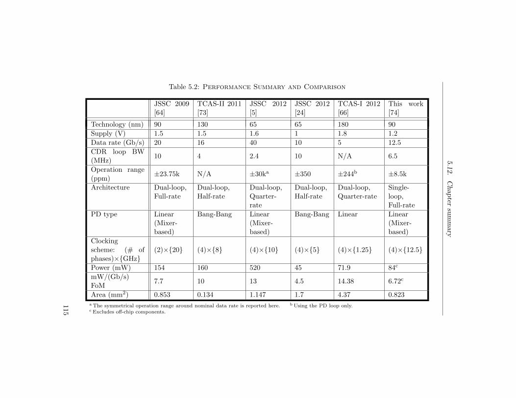
5.12.
Ch
apter
sum
mary
Table 5.2: Performance Summary and Comparison
JSSC 2009[64]
TCAS-II 2011[73]
JSSC 2012[5]
JSSC 2012[24]
TCAS-I 2012[66]
This work[74]
Technology (nm) 90 130 65 65 180 90
Supply (V) 1.5 1.5 1.6 1 1.8 1.2
Data rate (Gb/s) 20 16 40 10 5 12.5
CDR loop BW(MHz)
10 4 2.4 10 N/A 6.5
Operation range(ppm)
±23.75k N/A ±30ka ±350 ±244b ±8.5k
Architecture Dual-loop,Full-rate
Dual-loop,Half-rate
Dual-loop,Quarter-rate
Dual-loop,Half-rate
Dual-loop,Quarter-rate
Single-loop,Full-rate
PD type Linear(Mixer-based)
Bang-Bang Linear(Mixer-based)
Bang-Bang Linear Linear(Mixer-based)
Clockingscheme: (# ofphases)×GHz
(2)×20 (4)×8 (4)×10 (4)×5 (4)×1.25 (4)×12.5
Power (mW) 154 160 520 45 71.9 84c
mW/(Gb/s)FoM
7.7 10 13 4.5 14.38 6.72c
Area (mm2) 0.853 0.134 1.147 1.7 4.37 0.823a The symmetrical operation range around nominal data rate is reported here. b Using the PD loop only.c Excludes off-chip components.
115
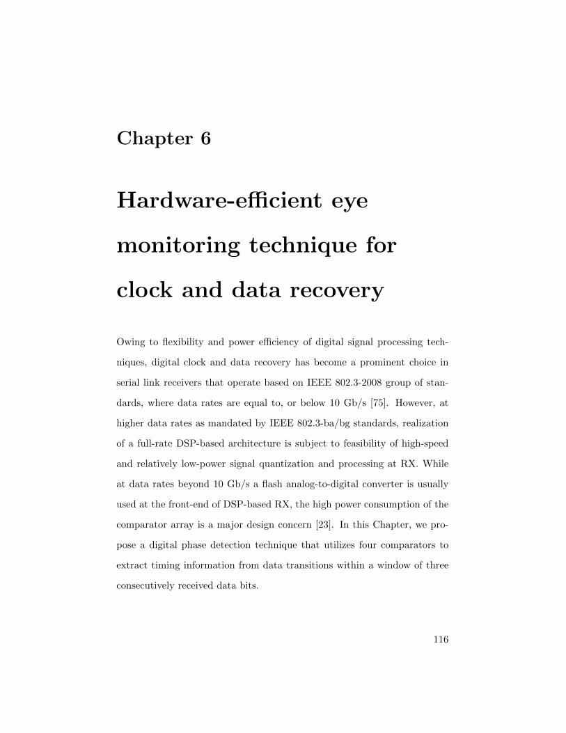
Chapter 6
Hardware-efficient eye
monitoring technique for
clock and data recovery
Owing to flexibility and power efficiency of digital signal processing tech-
niques, digital clock and data recovery has become a prominent choice in
serial link receivers that operate based on IEEE 802.3-2008 group of stan-
dards, where data rates are equal to, or below 10 Gb/s [75]. However, at
higher data rates as mandated by IEEE 802.3-ba/bg standards, realization
of a full-rate DSP-based architecture is subject to feasibility of high-speed
and relatively low-power signal quantization and processing at RX. While
at data rates beyond 10 Gb/s a flash analog-to-digital converter is usually
used at the front-end of DSP-based RX, the high power consumption of the
comparator array is a major design concern [23]. In this Chapter, we pro-
pose a digital phase detection technique that utilizes four comparators to
extract timing information from data transitions within a window of three
consecutively received data bits.
116

6.1. Digital clock recovery methods
CD1
CE
CD2
CDData sampleEdge sample
THi range in baud-rate ADC-based CDRs
Proposed (DTi , THi)
(a)
Δt1 Δt2
Δv1 Δv2C2
C3C4
C1
θ>0θ<0
(b)
Figure 6.1: The arrangement of DT i and TH i for comparators in binaryand ADC-based CDRs (a), and the arrangement in proposed CDR (b).
6.1 Digital clock recovery methods
Considering the decision time of comparators, DT i, where i is the identify-
ing tag of each comparator, conventional digital clock recovery methods fall
into two categories, namely, baud-rate or over-sampling. In the former, dur-
ing each unit interval data is sampled once, whereas in the latter, sampling
is performed at multiple time instances within each UI. Additionally, based
117

6.2. Proposed CDR technique
on the number of comparators with different decision thresholds, TH i, CR
schemes can be regarded as either binary, where there is only one compar-
ison threshold, or ADC-based, where there are more than one comparison
thresholds. Two well-known combinations of DT i and TH i, are Alexander
(Bang-Bang) [76] and Mueller-Muller [33]; where the former is binary and
usually 2×-oversampled, and the latter is ADC-based and baud-rate. As
noted on the conceptual eye diagram of Fig. 6.1a, in Mueller-Muller CR,
CD1 and CD2 represent two groups of data-sampling comparators that op-
erate in the vicinity of the data levels. However, in Alexander CR, CD is
a single data-sampling comparator and CE is a single edge-sampling com-
parator.
6.2 Proposed CDR technique
Figure 6.1b shows the decision coordinates, (DT i, TH i), of four compara-
tors, Ci,i=1:4, as used in this work to monitor the equalized received data,
Deq; where
∆t1 = DT 3 −DT 1 = DT 4 −DT 2 (6.1)
∆t1 + ∆t2 = 1UI (6.2)
∆v1 = TH1 − TH2 = TH3 − TH4 (6.3)
118

6.2. Proposed CDR technique
Table 6.1: Phase detection truth table for the arrangementshown in Fig.6.1b.
C1C2C3C4
∆t1 Q ∆t2b ∆t1 > ∆t2
Dataa θ = 0 −∆t2 ≤ θ < 0 0 < θ ≤ ∆t2 θ < −∆t2 θ > ∆t2
000 0000 0000 0000 0000 0000
001 0000 0000 0001 0000 0011
010 1111 0111 1101 0011 1100
011 1111 0111 1111 0011 1111
100 0000 0100 0000 1100 0000
101 0000 0100 0001 1100 0011
110 1111 1111 1101 1111 1100
111 1111 1111 1111 1111 1111a bn−1bnbn+1
b ∆t1 less than, equal to, or larger than ∆t2
θ is the phase error, and ∆v2 is the vertical eye opening in Deq. Note that
the coordinates (DT i, TH i) are essentially defined by ∆t1 and ∆v1 values.
Each comparator samples Deq once in every UI. Such arrangement enables
extracting timing information from data transitions within a 3-UI window
of consecutively received data bits denoted by bn−1bnbn+1. At the nth UI,
the binary representation of analog signal Deq, bn, is the current bit, bn−1
is the previous bit, bn+1 is the next bit, and C1C2C3C4 is the 4-bit word
formed by the binary decisions of the four comparators. The phase detection
(PD) truth table for the comparator arrangement of Fig. 6.1b is provided
in Table 6.1. Column 1 shows the eight possible values for the 3-bit word
bn−1bnbn+1. Column 2 (θ = 0) represents the phase-locked state, columns
3 and 4 (0 < |θ| ≤ ∆t2) represent the vicinity-of-lock state, and columns
5 and 6 (|θ| > ∆t2) represent the out-of-lock state. While the C1C2C3C4
words in columns 3 and 4 are true for all possible relationships between ∆t1
119
6.2. Proposed CDR technique
THiPItune
Loop filter
Quadraturephase
generator
VCO PD
FD
Phase interpolator
Charge pumps
Ipd
Ifd
Comparators & CML logic
C3
C2
C1
C4
CML
logi
c
Linear equalizer
!I
!Q
VCOtune
!1
!2 Q
I
Recovered data
PI1
PI2
updo
wn
updo
wn
CPpd
CPfd
DeqChannel
Figure 6.2: The proposed CDR architecture; shaded blocks and signals areoff-chip.
and ∆t2, as explained later, only ∆t1 > ∆t2 is used in this work. To detect
all possible timing scenarios using the bn−1bnbn+1 sequence, the amount of
ISI equalization prior to phase detection should be enough to cancel the
significant pre-cursor and post-cursor ISI taps, except the first pre-cursor
tap, h−1, and first post-cursor tap, h1, in the channel impulse response.
However, if |h−1| and |h1| are too large, i.e., with a magnitude comparable
to that of the main tap of the channel, |h0|, a portion of them should be
canceled by the equalizer to open Deq eye such that (DT i, TH i) coordinates
can be set within the eye as in Fig. 6.1b. The specifications of ∆v1 and ∆t1
are discussed later in this Chapter.
The architecture of the proposed full-rate CDR is shown in Fig. 6.2. A
quadrature phase generator [57, 68] is used to split the differential clock from
VCO into in-phase, ΦI , and quadrature, ΦQ, components that are 90 out of
phase. Subsequently, the differential clock phases Φ1 and Φ2 that are needed
120

6.2. Proposed CDR technique
−0.5 −0.25 0 0.25 0.50
0.1
0.2
0.3
0.4
0.5
Phase error, θ (UI)
Prob
abili
ty o
f occ
urre
nce
A1: 0001 | 1101B1: 0100 | 0111C1: 0000 | 1111D1: 0011 | 1100
C1
A1B1
vicinity-of-lock
phase-locked
vicinity-of-lock
out-of-lockout-of-lock
D1 D1
(a)
−400 −200 0 200 4000
0.1
0.2
0.3
0.4
Data rate offset, Δ f (ppm)
Prob
abili
ty o
f occ
urre
nce
A2: 0001 | 1101B2: 0011 | 1100C2: 0000 | 1111D2: Adjusted C2 FA C2
FCFB
D2B2 A2
(b)
Figure 6.3: Phase detection characteristic (a), and frequency detection char-acteristic of the proposed CDR (b).
121

6.2. Proposed CDR technique
for setting DT 1,2 and DT 3,4 are generated by the phase interpolator block
which consists of two phase interpolator sub-blocks, namely, PI1 and PI2.
Both PI1 and PI2 share the external tuning current PItune; however, PI1
interpolates between ΦI and ΦQ, while PI2 interpolates between ΦI and ΦQ.
ΦI and ΦQ represent 180 out-of-phase versions of ΦI and ΦQ, respectively.
With this approach, Φ1 and Φ2 can be tuned such that 90 < Φ2−Φ1 < 270.
Note that
Φ2 − Φ1 = ∆t1 ×360
1UI(6.4)
Figure 6.4a shows the schematic of the PIs. The bias voltages Vb1 and Vb2
are generated using the PI control circuit shown in Fig. 6.4b. The main
function of the control circuit is to generate a differential signal from the
current PItune.
The C1C2C3C4 word is processed by phase detection and frequency detection
(FD) logic to control the up/down signals of PD charge pump, CP pd, and FD
charge pump, CP fd. While CDR is in the vicinity-of-lock state (columns
3 and 4 in Table 1), data recovery, i.e., recovering bn, is done based on
a majority vote among C1 to C4; i.e., the current bit (bn) is ‘1’ (‘0’) if
the majority of bits in C1C2C3C4 word are ‘1’ (‘0’). The logic block is
implemented using current-mode logic (CML) gates. Ipd and Ifd, which
are the output currents of CP pd and CP fd, are averaged using the CDR
loop filter, and adjust the control voltage of oscillator, V COtune. Figs.
6.3a and 6.3b show the PD and FD characteristics of the proposed CDR,
respectively. Each graph in these figures is associated with two values for
122

6.2. Proposed CDR technique
Vb1 Vb2
ΦIb[ΦQ]
ΦI[ΦQb]
ΦQ[ΦIb]
ΦQb[ΦI]
Φ1[Φ2]
Φ1b[Φ2b]
(a)
PItune Vb1 Vb2
(b)
Figure 6.4: The schematic of PI1 and [PI2] (a), and the control circuit forPIs (b).
123

6.2. Proposed CDR technique
C1C2C3C4, as one relates to ‘0’→‘1’ data transition and the other relates to
‘1’→‘0’ transition. In Fig. 6.3a, the words whose probability of occurrence
(PO) is shown in graphs A1 and B1, are used as indicators for 0 < θ ≤
∆t2 and −∆t2 ≤ θ < 0, respectively. Detecting either of 0011 or 1100
words, whose PO is shown in graph D1, indicates that CDR is in the out-
of-lock state. When CDR is in such state, Ipd is deactivated, and CDR
re-locks through adjusting Ifd based on the FD characteristic. In the FD
characteristic (Fig. 6.3b), the C1C2C3C4 words associated with graphs B2
and D2 are indicators of ∆f < 0 and ∆f > 0 states, respectively; where
∆f is the frequency offset of the recovered clock. When ∆f is in the range
indicated as FA in Fig. 6.3b, Ifd is deactivated since small frequency offsets
are trackable through tuning V COtune using Ipd. When ∆f is within the
ranges indicated as FB and FC in Fig. 6.3b, i.e., |∆f | is relatively large, the
current supplied to the loop filter is Ifd and therefore, V COtune is controlled
by FD logic. While CDR operates in region FB, on the occurrence of 0011
or 1100 words, Ifd,up current is supplied to the loop filter. However, in
region FC , although the occurrence of 0000 or 1111 words is an indication
of ∆f > 0, drawing Ifd,down current from loop filter based on occurrence of
these words saturates V COtune. This is due to the fact that as shown in
Fig. 6.3b, unlike graph B2, graph C2 has a non-zero PO over all ∆f values.
Hence, to allow for proper frequency detection, only those 0000 words that
are either preceded by 0001, or succeed by 1101 are used to control Ifd,down.
In contrast, a 1111 word is only used when it is either preceded by 1101,
or succeed by 0001. The PO of such adjustment is shown in graph D2 of
Fig. 6.3b.
124

6.2. Proposed CDR technique
Among the three possible configurations, ∆t1 < ∆t2, ∆t1 = ∆t2, and ∆t1 >
∆t2, this work utilizes ∆t1 > ∆t2 as it yields indicator words for out-of-
lock state, and provides codes that are unique to each one of the PD and
FD states. ∆t1 < ∆t2 and ∆t1 = ∆t2 configurations are avoided since the
former results in codes that are common among PD and FD states, and the
latter lacks out-of-lock indicator word(s). However, we still limit ∆t1 such
that ∆t1 / 1.25×∆t2. This ensures that the D1 graph in Fig. 6.3a has the
desired maximum PO of 0.25, while avoiding the unnecessary29 extension in
the span of region where POD1 > 0.
Based on the measured S-parameters of the channel used in the test setup,
and those of the external linear equalizer (LE), simulations are preformed in
Matlab to find the optimal placement of (DT i, TH i) coordinates within eye
of Deq. To converge to an optimal solution while considering the RX power
budget, the amount of peaking in LE is set to its minimum that provides
enough ∆v2, such that ensures a value for ∆v1 (∆v1 < ∆v2) exists for which
∆t1 > ∆t2; and PD and FD characteristics are symmetrical around θ = 0
and ∆f = 0 points, respectively. For a measured post-equalization loss
of 3.9 dB at Nyquist frequency, simulations yield ∆t1 = 1.24 × ∆t2, and
∆v1 = 0.69 × ∆v2; which are used to generate PD and FD characteristics
of CDR as shown in Figs 6.3a and 6.3b. Based on ∆t1 and ∆v1 values,
the DC voltages PItune, TH1,3, and TH2,4 are supposed to be calibrated
at the start of CDR operation. While such calibration can be performed
using a DSP core [52], its implementation is beyond the scope of this work.
29Note that D1 region serves as out-of-lock indicator, and does not provide informationregarding the sign of phase error.
125

6.3. Measurement results
Therefore, in this work, we have manually adjusted the PItune, TH1,3, and
TH2,4 voltages.
6.3 Measurement results
As a proof-of-concept, a 12.5 Gb/s CDR chip is designed and fabricated
in a 90-nm CMOS technology. Fig. 6.5a shows the die micrograph which
occupies 0.93×0.825 mm2 excluding the pads. The loop bandwidth of the
CDR is set to 5 MHz through an external loop filter. A 231 − 1 pseudo-
random binary sequence (PRBS) data with 3.9 dB attenuation at 6.25 GHz
is fed to the chip using high-speed probes. The measured eye diagram of
the recovered data is shown in Fig. 6.5b, which has a jitter of 16.9 ps,pp.
The recovered clock reveals a jitter of 1.13 ps,rms. The CDR achieves a bit
error rate (BER) of < 10−12 while tracking data rate offsets over a range of
4.57 Mb/s (±183 ppm), without the help of a separate frequency detection
mechanism. The on-chip blocks (excluding buffers) consume 277 mW from
a 1.2 V supply.
6.4 Chapter summary
An eye-monitoring CDR is proposed, in which, unlike the conventional sam-
pling CDRs, the comparators are positioned within the data eye. Figure 6.6
demonstrates the potential application of such CDR architecture in a digital
RX, where a CTLE is used to partially open the data eye to address the
conditions introduces in Section 6.2. The QCG block proposed in Chapter
4 is used to provide the inputs of phase interpolators. The proposed phase-
126
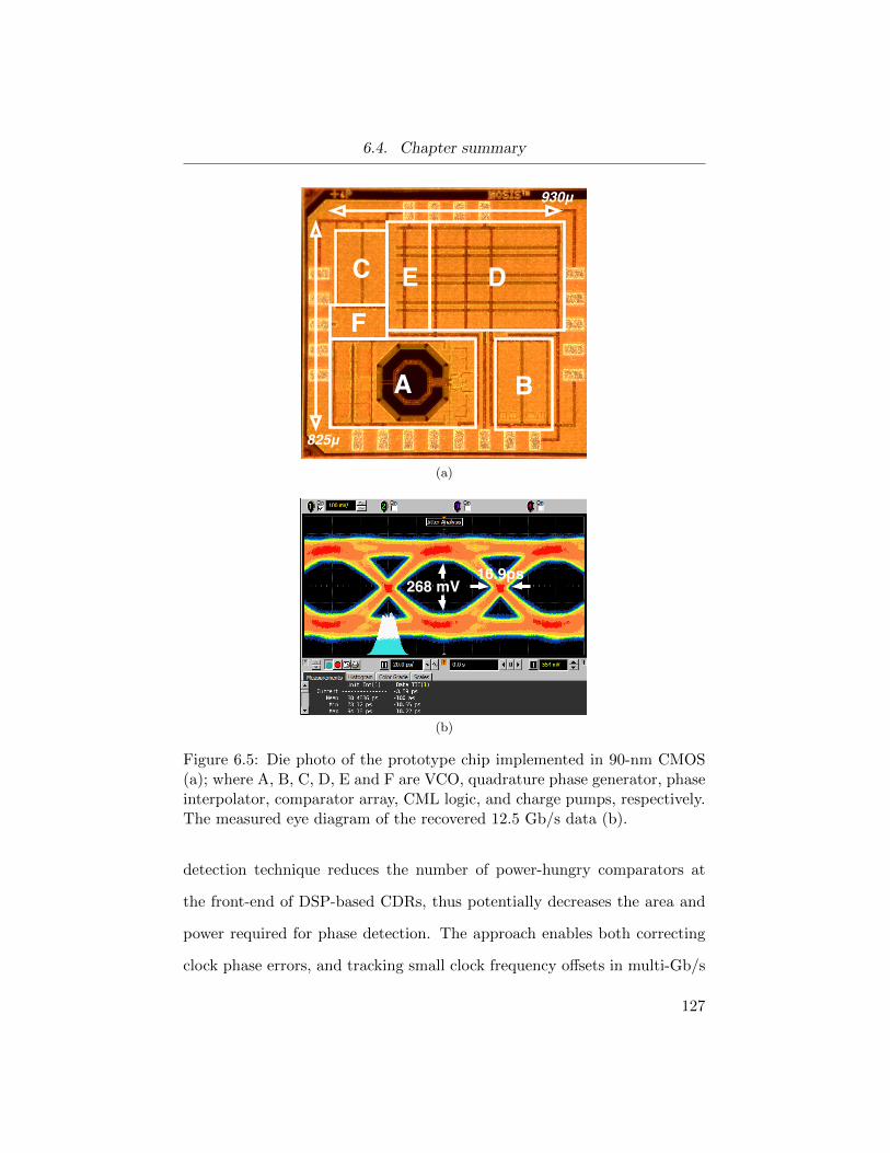
6.4. Chapter summary
A B
825μ
930μ
DEF
C
(a)
268 mV16.9ps
(b)
Figure 6.5: Die photo of the prototype chip implemented in 90-nm CMOS(a); where A, B, C, D, E and F are VCO, quadrature phase generator, phaseinterpolator, comparator array, CML logic, and charge pumps, respectively.The measured eye diagram of the recovered 12.5 Gb/s data (b).
detection technique reduces the number of power-hungry comparators at
the front-end of DSP-based CDRs, thus potentially decreases the area and
power required for phase detection. The approach enables both correcting
clock phase errors, and tracking small clock frequency offsets in multi-Gb/s
127
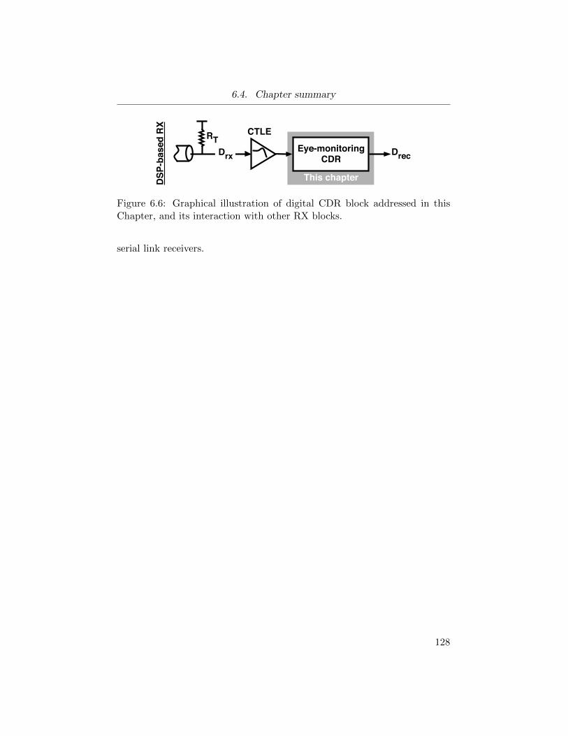
6.4. Chapter summary
This chapter
Drx
RTCTLE
Eye-monitoring CDR
DrecD
SP-b
ased
RX
Figure 6.6: Graphical illustration of digital CDR block addressed in thisChapter, and its interaction with other RX blocks.
serial link receivers.
128
Chapter 7
Conclusion
7.1 Research contributions
This thesis addresses some of the system-level and circuit-level challenges
associated with reducing the power consumption of multi-Gb/s wireline re-
ceivers. Several key functions of an RX, including equalization, clock recov-
ery, and generating multiple phases of the clock have been analyzed. The
following are the key contributions of this thesis (as partially published in
[32, 53, 68, 74, 77]):
• The power consumption of high speed DFEs is examined and a solution
to integrate the DFE within the front-end ADC is proposed. The
idea is validated through implementing a 10 Gb/s DSP-based RX in
a 65 nm CMOS technology.
• The DSP-based RX operates based on the proposed speculative/SAR
digitization algorithm, which is specifically designed for wireline ap-
plications. The algorithm allows for digitizing and recovering the data
using two comparators. Decision feedback equalization is achieved as
a natural product of this algorithm. The RX chip demonstrates the
feasibility of digitizing a 10 Gb/s data stream with 5 bits of resolu-
129
7.1. Research contributions
tion using 2 comparators, versus 31 (25 − 1) comparators needed in a
full-flash font-end ADC.
• Techniques and challenges of quadrature clock generation are analyzed.
An open-loop architecture based on active delay stages is proposed.
The power consumption of delay stages is investigated and a circuit-
level design technique is suggested which allows to achieve the desired
delay at certain clock frequency, while minimizing the power consump-
tion. The proposed architecture is embedded within both analog and
digital CDRs, and its performance is evaluated.
• An analog CDR, which utilizes a mixer-based PD is proposed. Using
the developed QCG block, a method for wideband data phase shifting
is implemented. While the prototype 90 nm chip contains a 12.5 Gb/s
version of this architecture, the architecture is suited for higher data
rates were an ADC-based front-end is not feasible.
• A hardware-efficient digital CDR architecture is proposed that en-
ables monitoring, and tracking the phase and frequency of the random
data. The architecture utilizes 4 comparators that are clocked from
the phases generated by QCG block. The comparators monitor the
data eye at baud-rate, and provide a digital 4-bit word that is sub-
sequently used to extract (recover) the phase and frequency of the
clock. The 12.5 Gb/s prototype CDR, implemented in 90 nm CMOS,
demonstrates a system level solution to reduce the comparator count.
Unlike the conventional ADC-based RX which choose the number of
comparators based on the required digitization resolution, in the pro-
130
7.2. Performance comparison
posed approach the comparator count is fundamentally set based on
the shape of the data eye formed by the eight possible combinations
of three consecutive bits. While avoiding data digitization, the digital
eye-monitoring CDR allows for detecting phase and frequency offsets
in the sampling clock in respect to the data eye.
7.2 Performance comparison
To choose the optimum RX architecture for a serial link, in addition to
power consumption, one should consider the BER and jitter performance of
the potential CDRs compatible with chosen RX topology. For the BER of
an RX we can write [78]
BER = 0.5× erfc(
WC1√2σnoise
)(7.1)
where WC1, and σnoise are worst case amplitude of the bit ‘1’ at sampling
time instance, and RMS noise voltage. Note that σnoise represents both
thermal voltage noise, and the voltage noise to to the random jitter in sam-
pling clock, RJclk. To convert the RMS value of RJclk, σclk, to σnoise we
can write [58]
σnoise =vsw × 2πfclk × σclk√
2(7.2)
where vsw is the signal swing. On the other hand, to calculate the contribu-
tion of data dependent jitter, DDJ30, to σclk, for bang-band CDR we can
30Or equivalently jitter due to ISI.
131
7.2. Performance comparison
write [79]
σclk =
√√2πθstepσddj
8(7.3)
θstep is the phase step of the CDR loop per decision cycle of PD, and has
the following relationship with the phase step of a binary bang-bang PD,
θstep,b,
θstep =θstep,b2n − 1
(7.4)
in which, n represents the sampling resolution. Additionally, for a linear
CDR (i.e. one with mixer-based PD) we have [80]
σclk = σddj
√3ωntbit√
2(7.5)
where ωn, and tbit are the natural frequency of the CDR loop, and duration
of each bit, respectively. Figure 7.1 compares the sampling time margin
versus amount of residual ISI in data, among bang-bang CDRs with various
resolutions in data and edge samplers, linear CDR (Chapter 5), and eye
monitoring CDR (Chapter 6). In Fig. 7.1, BER=10−12 has been considered
which simplifies Eq. 7.1 to
WC1 = 7× σn (7.6)
Figure 7.1 suggests that the sampling time margin for bang-bang CDRs
improves if the resolution of data/edge samplers increases. For large values
132

7.2. Performance comparison
−20 −15 −10 −5 0
0
0.2
0.4
0.6
0.8
1
Signal attenuation at Nyquist (dB)
Sam
plin
g tim
e m
argi
n (U
I)
BB, n=1BB, n=2BB, n=3BB, n=4BB, n=5LinearEM
Figure 7.1: Comparison of the sampling time margin of bang-bang CDR,analog CDR (with mixer-based PD), and eye monitoring CDR, as functionof different amounts of residual ISI in signal. BB, and EM refer to bang-bangand eye monitoring architectures.
of n, the power penalty of samplers may be partially offset by the lower
power consumption in CTLE. This is due to the fact that for a constant
BER, higher sampling resolution allows to tolerate more loss, and hence,
reduce the peaking demanded from CTLE. Additionally, note that if the
frequency response of channel has deep notches (i.e., due to via stubs),
equalization using CTLE may not be the feasible/optimal approach, and a
multi-tap high-resolution DFE may be inevitable.
From Fig. 7.1 we can see that a linear analog CDR typically offers lower
sampling time margin at left half of the signal loss spectrum, as the high
residual ISI in data modulates the gain of the mixer-based PD and results
133

7.2. Performance comparison
Table 7.1: Selection of CDR architecture based on channelloss
Channel loss at Nyquist CDR architecture
Low Bang-bang (low-resolution)a
Low-Medium Linear (Mixer-based)
Medium-High Eye monitoring
High Bang-bang (high-resolution)a Although linear CDR provides a marginally better jitter performance in this category, itmight not be as area efficient.
in excessive jitter. However, for the right side of the signal loss spectrum
(i.e., low loss channels), linear PDs prove to be a superior choice as they not
prone to the power versus sampling resolution trade-off of a digital RX.
Finally, the eye monitoring CDR proves useful when data has higher residual
ISI (i.e. higher σddj). This can be explained by considering that the timing-
threshold coordinates (DT i, TH i) of comparators are located within the
data eye as opposed to the sampling scheme where they are distributed
in the range set by ISI. While this is beneficial for lossy channels31, the
timing margin of such CDR architecture is fundamentally limited by the
∆t1 / 1.25×∆t2 condition discussed in Chapter 6 (i.e., the flat region of
the corresponding time margin curve in Fig. 7.1). This partially diminishes
the advantage of such architecture while communicating through low-loss
channels. Table 7.1 summarizes the above discussion.
31Because DDJ does not modulate the bit decision of the comparators
134

7.3. Future work
7.3 Future work
The channel characteristics, data transmission rate, and power budget are
three main factors which should be considered in the design process of mod-
ern wireline RX. The first factor is usually dictated by the network infras-
tructure, the second factor is set by the particular standard of operation,
and the last factor depends on the application and operation medium (e.g.,
chip-to-chip versus long-haul links). While the wireline channels have ex-
perienced relatively minor improvements over the years, wireline data rates
have constantly increased in each generation of IEEE 802.3 group of stan-
dards. Although power consumption is mostly a degree of freedom in the
design process, it is indeed the most prominent differentiating factor among
RX is the same class. Therefore, reducing the power dissipation of wireline
RX (and TX), is expected to remain an interesting area of research. Note
that although the proposed techniques are targeted towards wireline RX,
with minor modification, they can be employed at the baseband of wireless
RX too. The following items are the potential future tasks that can be done
to exploit the results of this thesis, and further enhance the power versus
performance trade-off in both analog and digital RX:
• While offering great flexibility and enhancing sophisticated digital sig-
nal processing, an ADC-based RX architecture is still not considered
an optimal solution at very high data rates (e.g., > 25 Gb/s). One
can further minimize the power consumption through exploiting high-
speed comparator architectures other than CML. The main challenge
would be providing a sampling and conversion speed at least equal to
135
7.3. Future work
baud rate; a difficult task beyond 10 Gb/s.
• The trade-off between achieving sharp edges at comparator output ver-
sus having low comparator latency remains a challenge. Specifically,
the delay of cascaded latches may introduce large latencies, which may
not be tolerated if the comparator falls within the timing critical loop
of DFE. In such scenario, reducing comparator latency to a small por-
tion of UI would be necessary; otherwise, either the timing would be
violated at the summing node, or less than optimal settling time would
result in digitization (quantization) error.
• While this thesis focuses on binary signaling, it should be noted that
multi-level signaling is an active area of research. An advantage of
ADC-based RX over binary RX is that it can recover both binary
and multi-level data with minimal adjustment to the DSP-based al-
gorithm; whereas in an analog RX, the hardware should be mostly
redesigned. The proposed speculative/SAR digitization algorithm can
be modified to accommodate multiple data levels. Furthermore, adap-
tively adjusting the comparator thresholds to digitize > 25 Gb/s data
streams poses interesting challenges.
• In applications that require dense arrays of TX/RX pairs, realizing
a separate QCG block for each transceiver may not be area efficient.
On the other hand, if transceivers share the QCG, maintaining the
integrity of quadrature clock phases over long distances is challeng-
ing. Finding an algorithm for distributing an optimal number of QCG
blocks within a large chip is a notable design challenge.
136

Bibliography
[1] Cisco visual networking index: Cisco Visual Networking In-
dex: Forecast and Methodology, 2011–2016. [Online]. Available:
http://www.cisco.com/en/US/solutions/collateral/ns341/ns525/
ns537/ns705/ns827/white paper c11-481360 ns827 Networking
Solutions White Paper.html
[2] G. Balamurugan, J. Kennedy, G. Banerjee, J. Jaussi, M. Mansuri,
F. O’Mahony, B. Casper, and R. Mooney, “A scalable 5-15 Gbps, 14-75
mW low-power I/O transceiver in 65 nm CMOS,” Solid-State Circuits,
IEEE Journal of, vol. 43, no. 4, pp. 1010–1019, 2008.
[3] K.-Y. K. Chang, J. Wei, C. Huang, Y. Li, K. Donnelly, M. Horowitz,
Y. Li, and S. Sidiropoulos, “A 0.4-4 Gb/s CMOS quad transceiver cell
using on-chip regulated dual-loop PLLs,” Solid-State Circuits, IEEE
Journal of, vol. 38, no. 5, pp. 747–754, 2003.
[4] K. Chang, S. Pamarti, K. Kaviani, E. Alon, X. Shi, T. J. Chin,
J. Shen, G. Yip, C. Madden, R. Schmitt, C. Yuan, F. Assaderaghi,
and M. Horowitz, “Clocking and circuit design for a parallel I/O on a
first-generation CELL processor,” in Solid-State Circuits Conference,
137

Bibliography
2005. Digest of Technical Papers. ISSCC. 2005 IEEE International,
2005, pp. 526–615 Vol. 1.
[5] M.-S. Chen, Y.-N. Shih, C.-L. Lin, H.-W. Hung, and J. Lee, “A fully-
integrated 40-Gb/s transceiver in 65-nm CMOS technology,” JSSC,
vol. 47, no. 3, pp. 627–640, Mar. 2012.
[6] J.-K. Kim, J. Kim, G. Kim, and D.-K. Jeong, “A fully integrated 0.13-
µm CMOS 40-Gb/s serial link transceiver,” Solid-State Circuits, IEEE
Journal of, vol. 44, no. 5, pp. 1510–1521, 2009.
[7] D. Cui, B. Raghavan, U. Singh, A. Vasani, Z. Huang, D. Pi, M. Khan-
pour, A. Nazemi, H. Maarefi, T. Ali, N. Huang, W. Zhang, B. Zhang,
A. Momtaz, and J. Cao, “A dual 23Gb/s CMOS transmitter/receiver
chipset for 40Gb/s RZ-DQPSK and CS-RZ-DQPSK optical transmis-
sion,” in Solid-State Circuits Conference Digest of Technical Papers
(ISSCC), 2012 IEEE International, 2012, pp. 330–332.
[8] K. Fukuda, H. Yamashita, G. Ono, R. Nemoto, E. Suzuki, N. Masuda,
T. Takemoto, F. Yuki, and T. Saito, “A 12.3-mW 12.5-Gb/s complete
transceiver in 65-nm CMOS process,” Solid-State Circuits, IEEE Jour-
nal of, vol. 45, no. 12, pp. 2838–2849, 2010.
[9] J. Bulzacchelli, M. Meghelli, S. Rylov, W. Rhee, A. Rylyakov,
H. Ainspan, B. Parker, M. Beakes, A. Chung, T. Beukema, P. Pepelju-
goski, L. Shan, Y. Kwark, S. Gowda, and D. Friedman, “A 10-Gb/s
5-tap DFE/4-tap FFE transceiver in 90-nm CMOS technology,” Solid-
State Circuits, IEEE Journal of, vol. 41, no. 12, pp. 2885–2900, 2006.
138

Bibliography
[10] F. Spagna, L. Chen, M. Deshpande, Y. Fan, and D. Gambetta, “A
78mW 11.8Gb/s serial link transceiver with adaptive RX equalization
and baud-rate CDR in 32nm CMOS,” in ISSCC, Feb. 2010, pp. 366–
367.
[11] K. Fukuda, H. Yamashita, F. Yuki, M. Yagyu, R. Nemoto, T. Take-
moto, T. Saito, N. Chujo, K. Yamamoto, H. Kanai, and A. Hayashi,
“An 8Gb/s transceiver with 3x-oversampling 2-threshold eye-tracking
CDR circuit for -36.8dB-loss backplane,” in Solid-State Circuits Con-
ference, 2008. ISSCC 2008. Digest of Technical Papers. IEEE Interna-
tional, 2008, pp. 98–598.
[12] N. Kocaman, A. Garg, B. Raghavan, D. Cui, A. Vasani, K. Tang,
D. Pi, H. Tong, S. Fallahi, W. Zhang, U. Singh, J. Cao, B. Zhang,
and A. Momtaz, “11.3 Gbps CMOS SONET compliant transceiver for
both RZ and NRZ applications,” Solid-State Circuits, IEEE Journal
of, vol. 46, no. 12, pp. 3089–3100, 2011.
[13] K.-I. Oh, L.-S. Kim, K.-I. Park, Y.-H. Jun, J.-S. Choi, and K. Kim,
“A 5-Gb/s/pin transceiver for DDR memory interface with a crosstalk
suppression scheme,” Solid-State Circuits, IEEE Journal of, vol. 44,
no. 8, pp. 2222–2232, 2009.
[14] S. Palermo, A. Emami-Neyestanak, and M. Horowitz, “A 90 nm CMOS
16 Gb/s transceiver for optical interconnects,” Solid-State Circuits,
IEEE Journal of, vol. 43, no. 5, pp. 1235–1246, 2008.
[15] J. Poulton, R. Palmer, A. Fuller, T. Greer, J. Eyles, W. Dally, and
139
Bibliography
M. Horowitz, “A 14-mW 6.25-Gb/s transceiver in 90-nm CMOS,” Solid-
State Circuits, IEEE Journal of, vol. 42, no. 12, pp. 2745–2757, 2007.
[16] J. Proesel, C. Schow, and A. Rylyakov, “25Gb/s 3.6pJ/b and 15Gb/s
1.37pJ/b VCSEL-based optical links in 90nm CMOS,” in Solid-State
Circuits Conference Digest of Technical Papers (ISSCC), 2012 IEEE
International, 2012, pp. 418–420.
[17] I. Young, E. Mohammed, J. Liao, A. Kern, S. Palermo, B. Block,
M. Reshotko, and P. L. D. Chang, “Optical I/O technology for tera-
scale computing,” Solid-State Circuits, IEEE Journal of, vol. 45, no. 1,
pp. 235–248, 2010.
[18] A. Amirkhany, A. Abbasfar, J. Savoj, M. Jeeradit, B. Garlepp, R. Kol-
lipara, V. Stojanovic, and M. Horowitz, “A 24 Gb/s software pro-
grammable analog multi-tone transmitter,” Solid-State Circuits, IEEE
Journal of, vol. 43, no. 4, pp. 999–1009, 2008.
[19] J.-Y. Song and O.-K. Kwon, “Low-power 10-Gb/s transmitter for high-
speed graphic DRAMs using 0.18-µm CMOS technology,” Circuits and
Systems II: Express Briefs, IEEE Transactions on, vol. 58, no. 12, pp.
921–925, 2011.
[20] Y.-H. Song and S. Palermo, “A 6-Gbit/s hybrid voltage-mode trans-
mitter with current-mode equalization in 90-nm CMOS,” Circuits and
Systems II: Express Briefs, IEEE Transactions on, vol. 59, no. 8, pp.
491–495, 2012.
140

Bibliography
[21] K.-L. Wong, H. Hatamkhani, M. Mansuri, and C.-K. Yang, “A 27-
mW 3.6-Gb/s I/O transceiver,” Solid-State Circuits, IEEE Journal of,
vol. 39, no. 4, pp. 602–612, 2004.
[22] A. Agrawal, A. Liu, P. Hanumolu, and G.-Y. Wei, “An 8×5 Gb/s par-
allel receiver with collaborative timing recovery,” Solid-State Circuits,
IEEE Journal of, vol. 44, no. 11, pp. 3120–3130, 2009.
[23] E.-H. Chen, R. Yousry, and C.-K. Yang, “Power optimized ADC-based
serial link receiver,” JSSC, vol. 47, no. 4, pp. 938 –951, April 2012.
[24] C. Thakkar, L. Kong, K. Jung, A. Frappe, and E. Alon, “A 10 Gb/s
45 mW adaptive 60 GHz baseband in 65 nm CMOS,” JSSC, vol. 47,
no. 4, pp. 952–968, Apr. 2012.
[25] A. Sheikholeslami, “Multi-level signaling for chip-to-chip and backplane
communication (a tutorial),” in ISMVL, May 2009, pp. 203–207.
[26] J. Proakis and M. Salehi, Digital Communications, 5th ed. New York,
NY, USA: McGraw-Hill, Inc., 2008.
[27] M. Harwood, N. Warke, R. Simpson, T. Leslie, and S. Batty, “A
12.5Gb/s SerDes in 65nm CMOS using a baud-rate ADC with digi-
tal receiver equalization and clock recovery,” in ISSCC, Feb. 2007, pp.
436–437.
[28] H. Toyoda, G. Ono, and S. Nishimura, “100GbE PHY and MAC layer
implementations,” Communications Magazine, IEEE, vol. 48, no. 3, pp.
S41–S47, March 2010.
141
Bibliography
[29] B. Abiri, A. Sheikholeslami, H. Tamura, and M. Kibune, “An adapta-
tion engine for a 2x blind ADC-Based CDR in 65 nm CMOS,” JSSC,
vol. 46, no. 12, pp. 3140 –3149, dec. 2011.
[30] M.-S. Chen, Y.-N. Shih, C.-L. Lin, H.-W. Hung, and J. Lee, “A 40Gb/s
TX and RX chip set in 65nm CMOS,” in ISSCC, Feb. 2011, pp. 146–
148.
[31] S. Quan, F. Zhong, W. Liu, P. Aziz, T. Jing, J. Dong, C. Desai,
H. Gao, M. Garcia, G. Hom, T. Huynh, H. Kimura, R. Kothari, L. Li,
C. Liu, S. Lowrie, K. Ling, A. Malipatil, R. Narayan, T. Prokop,
C. Palusa, A. Rajashekara, A. Sinha, C. Zhong, and E. Zhang,
“A 1.0625-to-14.025Gb/s multimedia transceiver with full-rate source-
series-terminated transmit driver and floating-tap decision-feedback
equalizer in 40nm CMOS,” in ISSCC, feb. 2011, pp. 348 –350.
[32] A. Zargaran-Yazd, S. Mirabbasi, and R. Saleh, “A 10 Gb/s low-power
SerDes receiver based on a hybrid speculative/SAR digitization tech-
nique,” in ISCAS, may 2011, pp. 446 –449.
[33] K. Mueller and M. Muller, “Timing recovery in digital synchronous data
receivers,” Communications, IEEE Transactions on, vol. 24, no. 5, pp.
516–531, May 1976.
[34] W. Sansen, Analog Design Essentials. Springer, 2006.
[35] Y. Hidaka, W. Gai, T. Horie, J. H. Jiang, Y. Koyanagi, and H. Osone,
“A 4-channel 1.25-10.3 Gb/s backplane transceiver macro with 35 dB
142

Bibliography
equalizer and sign-based zero-forcing adaptive control,” JSSC, vol. 44,
no. 12, pp. 3547 –3559, dec. 2009.
[36] A. Sheikholeslami, B. Payne, and J. Lin, “Will ADCs overtake binary
frontends in backplane signaling (special evening session, se3),” ISSCC,
p. 514, feb 2009.
[37] C.-K. K. Yang and E.-H. Chen, “ADC-based serial I/O receivers,” in
CICC, Sept. 2009, pp. 323–330.
[38] O. Ishida, “40/100GbE technologies and related activities of IEEE stan-
dardization,” in Optical Fiber Communication - incudes post deadline
papers, 2009. OFC 2009. Conference on, March, pp. 1–29.
[39] B. Murmann. (2012) ADC Performance Survey 1997-2012. [Online].
Available: http://www.stanford.edu/∼murmann/adcsurvey.html
[40] O. Tyshchenko, A. Sheikholeslami, H. Tamura, M. Kibune, and
J. Ogawa, “A 5-Gb/s ADC-based feed-forward CDR in 65 nm CMOS,”
JSSC, vol. 45, no. 6, pp. 1091–1098, jun. 2010.
[41] A. Varzaghani and C.-K. Yang, “A 4.8 GS/s 5-bit ADC-based receiver
with embedded DFE for signal equalization,” JSSC, vol. 44, no. 3, pp.
901–915, March 2009.
[42] O. Agazzi, M. Hueda, D. Crivelli, H. Carrer, and G. Luna, “A 90 nm
CMOS DSP MLSD transceiver with integrated AFE for electronic dis-
persion compensation of multimode optical fibers at 10 Gb/s,” JSSC,
vol. 43, no. 12, pp. 2939–2957, Dec. 2008.
143
Bibliography
[43] P. Schvan, J. Bach, C. Fait, P. Flemke, and R. Gibbins, “A 24GS/s 6b
ADC in 90nm CMOS,” in ISSCC, Feb. 2008, pp. 544–545.
[44] Y. Greshishchev, J. Aguirre, M. Besson, R. Gibbins, and P. Flemke, “A
40GS/s 6b ADC in 65nm CMOS,” in ISSCC, Feb. 2010, pp. 390–391.
[45] B. Murmann, “A/D converter trends: Power dissipation, scaling and
digitally assisted architectures,” in CICC, Sept. 2008, pp. 105–112.
[46] Y. Zhu, C.-H. Chan, U.-F. Chio, S.-W. Sin, and R. Martins, “A 10-bit
100-MS/s reference-free SAR ADC in 90 nm CMOS,” JSSC, vol. 45,
no. 6, pp. 1111–1121, jun. 2010.
[47] O. Agazzi and V. Gopinathan, “Background calibration of interleaved
analog to digital converters for high-speed communications using inter-
leaved timing recovery techniques,” in ISCAS, May 2005, pp. 1390–1393
Vol. 2.
[48] H.-I. Cong, J. Andrews, D. Boulin, S.-C. Fang, S. Hillenius, and
J. Michejda, “Multigigahertz CMOS dual-modulus prescaler IC,” JSSC,
vol. 23, no. 5, pp. 1189–1194, Oct.
[49] M. Choi and A. Abidi, “A 6-b 1.3-Gsample/s A/D converter in 0.35-µm
CMOS,” JSSC, vol. 36, no. 12, pp. 1847–1858, dec. 2001.
[50] C.-H. Lin and K. Bult, “A 10-b, 500-MSample/s CMOS DAC in 0.6
mm2,” JSSC, vol. 33, no. 12, pp. 1948–1958, dec. 1998.
[51] C.-H. Lin, F. van der Goes, J. Westra, J. Mulder, and K. Bult, “A 12
144

Bibliography
bit 2.9 GS/s DAC With IM3 60 dBc beyond 1 GHz in 65 nm CMOS,”
JSSC, vol. 44, no. 12, pp. 3285–3293, dec. 2009.
[52] J. Cao, B. Zhang, U. Singh, D. Cui, and A. Garg, “A 500mW digitally
calibrated AFE in 65nm CMOS for 10Gb/s serial links over backplane
and multimode fiber,” in ISSCC, Feb. 2009, pp. 370–371.
[53] A. Zargaran-Yazd and S. Mirabbasi, “Low-power design technique
for decision-feedback equalisation in serial links,” Electronics Letters,
vol. 48, no. 17, pp. 1042–1044, 2012.
[54] T. H. Lee, The Design of CMOS Radio-Frequency Integrated Circuits,
2nd ed. Cambridge University Press, 2003.
[55] B. Razavi, RF Microelectronics, 2nd ed. Prentice Hall, 2011.
[56] A. Mazzanti and P. Andreani, “A time-variant analysis of fundamental
phase noise in cmos parallel -tank quadrature oscillators,” Circuits and
Systems I: Regular Papers, IEEE Transactions on, vol. 56, no. 10, pp.
2173 –2180, oct. 2009.
[57] K. hyoun Kim, P. Coteus, D. Dreps, S. Kim, and S. Rylov, “A 2.6mW
370MHz-to-2.5GHz open-loop quadrature clock generator,” in ISSCC,
Feb. 2008, pp. 458–627.
[58] K. W. M. Tony Chan Carusone, David A. Johns, Analog Integrated
Circuit Design, 2nd ed. Wiley, 2011.
[59] K. S. D. Oh and X. C. C. Yuan, High-Speed Signaling: Jitter Modeling,
Analysis, and Budgeting. Prentice Hall, 2012.
145

Bibliography
[60] B. razavi, Design of Integrated Circuits for Optical Communications,
1st ed. McGraw-Hill Science, 2002.
[61] H. Lakdawala, X. Zhu, H. Luo, S. Santhanam, L. Carley, and G. Fedder,
“Micromachined high-Q inductors in a 0.18-µm copper interconnect
low-k dielectric CMOS process,” JSSC, vol. 37, no. 3, pp. 394 –403,
mar 2002.
[62] N. Ishihara and Y. Akazawa, “A monolithic 156 Mb/s clock and data re-
covery PLL circuit using the sample-and-hold technique,” JSSC, vol. 29,
no. 12, pp. 1566 –1571, dec 1994.
[63] M. ta Hsieh and G. Sobelman, “Architectures for multi-Gb wire-linked
clock and data recovery,” Circuits and Systems Magazine, IEEE, vol. 8,
no. 4, pp. 45–57, quarter 2008.
[64] J. Lee and K.-C. Wu, “A 20-Gb/s full-rate linear clock and data recov-
ery circuit with automatic frequency acquisition,” JSSC, vol. 44, no. 12,
pp. 3590–3602, Dec. 2009.
[65] K.-C. Wu and J. Lee, “A 2 × 25-Gb/s receiver with 2:5 DMUX for
100-Gb/s Ethernet,” JSSC, vol. 45, no. 11, pp. 2421–2432, Nov. 2010.
[66] Y. S. Tan, K. S. Yeo, C. C. Boon, and M. A. Do, “A dual-loop clock
and data recovery circuit with compact quarter-rate CMOS linear phase
detector,” TCAS-I, vol. 59, no. 6, pp. 1156–1167, Jun. 2012.
[67] C. Liang and B. Razavi, “Transmitter linearization by beamforming,”
JSSC, vol. 46, no. 9, pp. 1956–1969, Sept. 2011.
146

Bibliography
[68] A. Zargaran-Yazd and S. Mirabbasi, “A 25 Gb/s full-rate CDR circuit
based on quadrature phase generation in data path,” in ISCAS, May
2012, pp. 317–320.
[69] B. Gilbert, “A precise four-quadrant multiplier with subnanosecond
response,” JSSC, vol. 3, no. 4, pp. 365–373, Dec. 1968.
[70] W. Kim, C. Seong, and W. Choi, “A 5.4Gb/s adaptive equalizer using
asynchronous-sampling histograms,” in ISSCC, Feb. 2011, pp. 358–359.
[71] H. Noguchi, N. Yoshida, H. Uchida, M. Ozaki, S. Kanemitsu, and
S. Wada, “A 40Gb/s CDR with adaptive decision-point control using
eye-opening-monitor feedback,” in ISSCC, Feb. 2008, pp. 228–609.
[72] H. Muthali, T. Thomas, and I. Young, “A CMOS 10-Gb/s SONET
transceiver,” JSSC, vol. 39, no. 7, pp. 1026 – 1033, july 2004.
[73] C.-L. Hsieh and S.-I. Liu, “A 1-16-Gb/s wide-range clock/data recovery
circuit with a bidirectional frequency detector,” TCAS-II, vol. 58, no. 8,
pp. 487–491, Aug. 2011.
[74] A. Zargaran-Yazd and S. Mirabbasi, “12.5-Gb/s full-rate CDR with
wideband quadrature phase shifting in data path,” Circuits and Sys-
tems II: Express Briefs, IEEE Transactions on, vol. 60, no. 6, pp. 297–
301, 2013.
[75] M. Talegaonkar, R. Inti, and P. Hanumolu, “Digital clock and data
recovery circuit design: Challenges and tradeoffs,” in Custom Integrated
Circuits Conference (CICC), 2011 IEEE, sept. 2011, pp. 1 –8.
147

[76] J. Alexander, “Clock recovery from random binary signals,” Electronics
Letters, vol. 11, no. 22, pp. 541 –542, 30 1975.
[77] A. Zargaran-Yazd, K. Keikhosravy, H. Rashtian, and S. Mirabbasi,
“Hardware-efficient phase-detection technique for digital clock and data
recovery,” Electronics Letters, vol. 49, no. 1, pp. 20 –22, 3 2013.
[78] S. Hall and H. Heck, Advanced Signal Integrity for High-Speed Digital
Designs. Wiley-IEEE Press, 2009.
[79] B. Razavi, Phase-Locking in Phase-Locking in High-Performance Sys-
tems. IEEE Press, 2003, ch. Designing Bang-Bang PLLs for Clock and
Data Recovery in Serial Data Transmission Systems.
[80] J. Buckwalter and A. Hajimiri, “Analysis and equalization of data-
dependent jitter,” JSSC, vol. 41, no. 3, pp. 607–620, March.
148
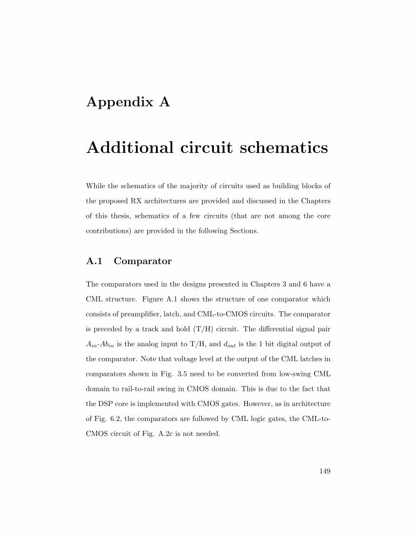
Appendix A
Additional circuit schematics
While the schematics of the majority of circuits used as building blocks of
the proposed RX architectures are provided and discussed in the Chapters
of this thesis, schematics of a few circuits (that are not among the core
contributions) are provided in the following Sections.
A.1 Comparator
The comparators used in the designs presented in Chapters 3 and 6 have a
CML structure. Figure A.1 shows the structure of one comparator which
consists of preamplifier, latch, and CML-to-CMOS circuits. The comparator
is preceded by a track and hold (T/H) circuit. The differential signal pair
Ain-Abin is the analog input to T/H, and dout is the 1 bit digital output of
the comparator. Note that voltage level at the output of the CML latches in
comparators shown in Fig. 3.5 need to be converted from low-swing CML
domain to rail-to-rail swing in CMOS domain. This is due to the fact that
the DSP core is implemented with CMOS gates. However, as in architecture
of Fig. 6.2, the comparators are followed by CML logic gates, the CML-to-
CMOS circuit of Fig. A.2c is not needed.
149

A.2. Digital-to-analog converter
T/HAin
Abin
Preamplifier 1st Latch 2nd Latch CML to CMOS
CML comparator
dout
Figure A.1: Block diagram of the CML comparator.
A.2 Digital-to-analog converter
Figure A.3 shows the schematic of a current steering DAC similar to the
one used in architecture of Fig. 3.5. Note that to avoid timing errors while
converting the digital bits dn,n=1:4 to the differential signals used to control
the gates of the steering devices in transconductance stages, an XOR gate
is used both as buffer (while one input is set to ‘0’) and as inverter (while
one input is set to ‘1’).
Additionally, to achieve a better linearity, the current sources in the DAC
are implanted in a thermometer-coded manner instead of the binary-wighted
alternative.
150

A.2. Digital-to-analog converter
Vbias
VOUTVOUTb
VIN VREFb VINbVREF
(a)
CLKbCLK
Vbias
VIN Track Hold
VOUTVOUTb
VINb
(b)
Vbias
VOUT
VIN VINb
(c)
Figure A.2: Preamplifier (a), latch (b), and CML-to-CMOS circuits.
151

A.2. Digital-to-analog converter
10d1d2d3d4
Aout
AboutIss
8×Iss
4×Iss
2×Iss
Figure A.3: Schematic of a 4-bit current steering DAC.
152