design, technology and characterization of micromechanised...
TRANSCRIPT

UNIVERSIDAD POLITÉCNICA DE MADRID
ESCUELA TÉCNICA SUPERIORDE INGENIEROS DE TELECOMUNICACIÓN
TESIS DOCTORAL
Design, Technology and Characterizationof Micromechanised Sensors and Actuators
for Harsh Environments
Eugenio Sillero Herrero2015


DEPARTAMENTO DE INGENIERÍA ELECTRÓNICA
ESCUELA TÉCNICA SUPERIORDE INGENIEROS DE TELECOMUNICACIÓN
TESIS DOCTORAL
Design, Technology and Characterizationof Micromechanised Sensors and Actuators
for Harsh Environments
AUTOR:Eugenio Sillero HerreroIngeniero de Telecomunicación
DIRECTOR:Fernando Calle Gómez
Doctor en Ciencias Físicas
2015


Tribunal nombrado por el Magfco. y Excmo. Sr. Rector de la Universidad Politécnica
de Madrid, el día de de 20 .
Presidente:
Secretario:
Vocal:
Vocal:
Vocal:
Realizando el acto de defensa y lectura de la Tesis el día de de 20 en
la Escuela Técnica Superior de Ingenieros de Telecomunicación, este Tribunal decide
otorgar la calificación de
EL PRESIDENTE EL SECRETARIO
LOS VOCALES


To Marina and ourlittle family.


Acknowledgements
I have to thank all the ISOM staff that has co-worked with me, either sharingtopic or sharing lab. It has been a real pleasure to work with all of you, students,technicians and professors. I owe special gratitude to my advisor, Fernando Calle,that has always supported me. A special mention is also owed to Sebastian Dubieland Javier Zugasti that have contributed to the work presented in this volume.
I also want to have a word about the people that opened their labs so I couldwork with them during my research years. First, the people I met at the TUD, Prof.Hartnagel, Prof. Pavlidis, Eunjung Cho, Sangyong Seo, Dr. Mutamba and OktayYilmazoglu. Of course I also remember the fantastic folk that I worked with at theIAF, specially Volker Cimalla, Vadim Lebedev, Oliver Williams, Claus-Christian Röhlig,Fabian Knöbber, Wilhelm Pfletcher, Waldemar Smirnov, Christoph Nebel and manyothers.
Finally, I must thank the wonderful family I have. They have supported andencouraged me along the whole path.


Contents
Contents xi
List of Figures xvii
List of Tables xxiii
Abstract xxv
Resumen xxvii
I Introduction and methodology 1
1 Introduction 31.1 Technologies for harsh environment MEMS and sensors . . . . . . . . . 41.2 Material selection criteria for MEMS . . . . . . . . . . . . . . . . . . . 7
1.2.1 Group III nitrides and their applications . . . . . . . . . . . . . 81.2.2 Diamond and its applications . . . . . . . . . . . . . . . . . . . 111.2.3 Material selection . . . . . . . . . . . . . . . . . . . . . . . . . . 14
1.3 Thesis objectives . . . . . . . . . . . . . . . . . . . . . . . . . . . . . . 151.3.1 Optimization of etching processes for the three dimensional
fabrication of nitride and diamond MEMS structures . . . . . . 161.3.2 Study of the mechanical and electrical properties of micromech-
anised structures . . . . . . . . . . . . . . . . . . . . . . . . . . 171.3.3 Development and characterization of NCD and nitride resonators
and sensors . . . . . . . . . . . . . . . . . . . . . . . . . . . . . 171.4 Thesis methodology . . . . . . . . . . . . . . . . . . . . . . . . . . . . 181.5 Thesis structure . . . . . . . . . . . . . . . . . . . . . . . . . . . . . . . 18
1.5.1 Notes about conventions . . . . . . . . . . . . . . . . . . . . . . 20
2 Design, fabrication and experimental techniques 212.1 Simulation tools . . . . . . . . . . . . . . . . . . . . . . . . . . . . . . 21
2.1.1 ANSYS finite element method SW . . . . . . . . . . . . . . . . . 212.1.2 Other software . . . . . . . . . . . . . . . . . . . . . . . . . . . 23
2.2 Fabrication techniques . . . . . . . . . . . . . . . . . . . . . . . . . . . 232.2.1 Epitaxial growth techniques . . . . . . . . . . . . . . . . . . . . 23
xi

xii CONTENTS
2.2.2 Chemical vapor deposition of NCD . . . . . . . . . . . . . . . . 252.2.3 Reactive sputtering . . . . . . . . . . . . . . . . . . . . . . . . . 272.2.4 Reactive ion etching . . . . . . . . . . . . . . . . . . . . . . . . 322.2.5 Wet etching . . . . . . . . . . . . . . . . . . . . . . . . . . . . . 352.2.6 Plasma enhanced chemical vapor deposition . . . . . . . . . . . 352.2.7 Metallization . . . . . . . . . . . . . . . . . . . . . . . . . . . . 36
2.3 Structural characterization . . . . . . . . . . . . . . . . . . . . . . . . . 372.3.1 X-ray diffraction . . . . . . . . . . . . . . . . . . . . . . . . . . 382.3.2 Scanning electron microscopy . . . . . . . . . . . . . . . . . . . 402.3.3 Atomic force microscopy . . . . . . . . . . . . . . . . . . . . . . 412.3.4 White light interferometry . . . . . . . . . . . . . . . . . . . . . 42
2.4 Optical characterization . . . . . . . . . . . . . . . . . . . . . . . . . . 442.4.1 Photoluminescence . . . . . . . . . . . . . . . . . . . . . . . . . 442.4.2 Raman spectroscopy . . . . . . . . . . . . . . . . . . . . . . . . 462.4.3 Fourier transform infrared spectroscopy . . . . . . . . . . . . . 47
2.5 Electrical characterization . . . . . . . . . . . . . . . . . . . . . . . . . 482.5.1 Current-voltage curves . . . . . . . . . . . . . . . . . . . . . . . 482.5.2 Capacitance-voltage curves . . . . . . . . . . . . . . . . . . . . 482.5.3 Characterization equipment . . . . . . . . . . . . . . . . . . . . 49
2.6 Electromechanical characterization . . . . . . . . . . . . . . . . . . . . 492.6.1 Beam deflection . . . . . . . . . . . . . . . . . . . . . . . . . . 492.6.2 Magnetomotive spectroscopy . . . . . . . . . . . . . . . . . . . 522.6.3 Piezoresponse characterization . . . . . . . . . . . . . . . . . . 542.6.4 Determination of piezoelectric properties of thin films . . . . . 58
II Manufacturing and material issues 59
3 Dry etching of functional materials 613.1 Dry etching of GaN . . . . . . . . . . . . . . . . . . . . . . . . . . . . . 62
3.1.1 Preliminary trials . . . . . . . . . . . . . . . . . . . . . . . . . . 623.1.2 Etch rate optimization . . . . . . . . . . . . . . . . . . . . . . . 633.1.3 Surface morphology . . . . . . . . . . . . . . . . . . . . . . . . 653.1.4 Profile morphology . . . . . . . . . . . . . . . . . . . . . . . . . 66
3.2 Dry etching of AlN . . . . . . . . . . . . . . . . . . . . . . . . . . . . . 673.2.1 Preliminary results . . . . . . . . . . . . . . . . . . . . . . . . . 683.2.2 Etch rate and selectivity to GaN . . . . . . . . . . . . . . . . . 693.2.3 Surface morphology . . . . . . . . . . . . . . . . . . . . . . . . 70
3.3 Dry etching of InN . . . . . . . . . . . . . . . . . . . . . . . . . . . . . 703.3.1 Residual accumulation on the etched surface . . . . . . . . . . 713.3.2 Etch rate and selectivity to GaN . . . . . . . . . . . . . . . . . 713.3.3 Surface morphology . . . . . . . . . . . . . . . . . . . . . . . . 72
3.4 Dry etching of AlInN lattice matched to GaN . . . . . . . . . . . . . . . 733.4.1 Etch conditions . . . . . . . . . . . . . . . . . . . . . . . . . . . 743.4.2 Etch rate and selectivity . . . . . . . . . . . . . . . . . . . . . . 753.4.3 Etched surface morphology . . . . . . . . . . . . . . . . . . . . 77

CONTENTS xiii
3.5 Nanocrystalline diamond etching . . . . . . . . . . . . . . . . . . . . . 773.5.1 Material description . . . . . . . . . . . . . . . . . . . . . . . . 783.5.2 Etching with Ti/Au/Ni masks . . . . . . . . . . . . . . . . . . . 78
3.6 Conclusions . . . . . . . . . . . . . . . . . . . . . . . . . . . . . . . . . 79
4 Patterning MEMS structures by sacrificial layer etching 834.1 Patterning of (Al, Ga)N/AlInN structures . . . . . . . . . . . . . . . . . 84
4.1.1 Wet etching of AlInN . . . . . . . . . . . . . . . . . . . . . . . . 844.1.2 Micromechanised GaN/AlInN structures . . . . . . . . . . . . . 91
4.2 Patterning of (Al, Ga)N/LT-AlN structures . . . . . . . . . . . . . . . . 924.2.1 Wet etching of LT-AlN . . . . . . . . . . . . . . . . . . . . . . . 934.2.2 Micromechanised GaN/LT-AlN structures . . . . . . . . . . . . . 95
4.3 Patterning of (Al, Ga, In)N/Si(111) structures . . . . . . . . . . . . . . 984.3.1 Wet isotropic etching of Si(111) . . . . . . . . . . . . . . . . . . 994.3.2 Dry isotropic etching of Si(111) . . . . . . . . . . . . . . . . . . 1014.3.3 Micromechanised (Al, Ga, In)N/Si(111) structures . . . . . . . 104
4.4 Conclusions . . . . . . . . . . . . . . . . . . . . . . . . . . . . . . . . . 106
5 AlN deposition by pulsed DC reactive sputtering 1095.1 Experimental procedure . . . . . . . . . . . . . . . . . . . . . . . . . . 1095.2 Deposition rate . . . . . . . . . . . . . . . . . . . . . . . . . . . . . . . 1115.3 Structural characterization . . . . . . . . . . . . . . . . . . . . . . . . . 112
5.3.1 X-Ray diffraction . . . . . . . . . . . . . . . . . . . . . . . . . . 1125.3.2 FTIR spectroscopy . . . . . . . . . . . . . . . . . . . . . . . . . 1145.3.3 Piezoresponse . . . . . . . . . . . . . . . . . . . . . . . . . . . . 1175.3.4 Surface morphology . . . . . . . . . . . . . . . . . . . . . . . . 118
5.4 Electrical characterization . . . . . . . . . . . . . . . . . . . . . . . . . 1195.4.1 Breakdown field measurements . . . . . . . . . . . . . . . . . . 1205.4.2 Current-Capacitance characteristics . . . . . . . . . . . . . . . . 1205.4.3 Current-Voltage characteristics . . . . . . . . . . . . . . . . . . 123
5.5 Capacitively coupled RF MEMS switches . . . . . . . . . . . . . . . . . 1245.6 Conclusions . . . . . . . . . . . . . . . . . . . . . . . . . . . . . . . . . 125
6 Nanoporous Gallium Nitride 1276.1 Porous material fabrication process description . . . . . . . . . . . . . 127
6.1.1 Etching basin description . . . . . . . . . . . . . . . . . . . . . 1286.1.2 UV illumination system description . . . . . . . . . . . . . . . . 129
6.2 Experimental conditions . . . . . . . . . . . . . . . . . . . . . . . . . . 1306.3 Morphology of the porous layers . . . . . . . . . . . . . . . . . . . . . 131
6.3.1 Etchings performed on samples without metallization . . . . . . 1316.3.2 Etchings performed on samples with Pt metallization . . . . . . 132
6.4 Optical properties . . . . . . . . . . . . . . . . . . . . . . . . . . . . . . 1336.5 Etching of porous layers . . . . . . . . . . . . . . . . . . . . . . . . . . 1366.6 Chemical properties . . . . . . . . . . . . . . . . . . . . . . . . . . . . 1386.7 Conclusions . . . . . . . . . . . . . . . . . . . . . . . . . . . . . . . . . 140

xiv CONTENTS
III Devices 143
7 III-N MEMS structures 1457.1 Introduction and motivation . . . . . . . . . . . . . . . . . . . . . . . . 145
7.1.1 Elastic modulus of thin nitride free-standing structures . . . . . 1477.2 Structure description . . . . . . . . . . . . . . . . . . . . . . . . . . . . 148
7.2.1 Buckling bridges for compressive stress determination . . . . . 1497.2.2 Stress pointers . . . . . . . . . . . . . . . . . . . . . . . . . . . 1507.2.3 Strain gauge . . . . . . . . . . . . . . . . . . . . . . . . . . . . 1517.2.4 H-Shaped beams . . . . . . . . . . . . . . . . . . . . . . . . . . 1517.2.5 Single clamped cantilevers . . . . . . . . . . . . . . . . . . . . . 1527.2.6 Structure selection . . . . . . . . . . . . . . . . . . . . . . . . . 153
7.3 Material and fabrication . . . . . . . . . . . . . . . . . . . . . . . . . . 1547.3.1 Material description . . . . . . . . . . . . . . . . . . . . . . . . 1547.3.2 GaN and AlGaN/GaN epitaxial layers on Si(111) . . . . . . . 1547.3.3 Fabrication of the microstructures . . . . . . . . . . . . . . . . . 156
7.4 Static characterization of Young’s modulus . . . . . . . . . . . . . . . . 1587.4.1 Elastic modulus of GaN . . . . . . . . . . . . . . . . . . . . . . 1587.4.2 Elastic modulus of AlN . . . . . . . . . . . . . . . . . . . . . . 1597.4.3 Elastic modulus of InN . . . . . . . . . . . . . . . . . . . . . . 1607.4.4 Result discussion . . . . . . . . . . . . . . . . . . . . . . . . . . 162
7.5 Residual stress and relaxation of free-standing structures . . . . . . . . 1637.5.1 Stress value and gradient of GaN and AlGaN/GaN epitaxial
layers on Si(111) . . . . . . . . . . . . . . . . . . . . . . . . . . 1647.5.2 Stress value and gradient of InN epitaxial layers on Si(111) . . 1667.5.3 Stress value and gradient of AlN epitaxial layers on Si(111) . . 168
7.6 Conclusions . . . . . . . . . . . . . . . . . . . . . . . . . . . . . . . . . 169
8 Nanocrystalline diamond resonators 1718.1 Introduction and motivation . . . . . . . . . . . . . . . . . . . . . . . . 1718.2 Structure fabrication . . . . . . . . . . . . . . . . . . . . . . . . . . . . 172
8.2.1 Free-standing structure description . . . . . . . . . . . . . . . . 1738.2.2 Resonator fabrication process . . . . . . . . . . . . . . . . . . . 1748.2.3 Material description . . . . . . . . . . . . . . . . . . . . . . . . 175
8.3 Static determination of the mechanical properties of NCD . . . . . . . 1768.3.1 Young’s modulus determination . . . . . . . . . . . . . . . . . . 1768.3.2 Metal layer stress determination . . . . . . . . . . . . . . . . . 179
8.4 Dynamic characterization of NCD microdevices . . . . . . . . . . . . . 1808.4.1 Previous considerations . . . . . . . . . . . . . . . . . . . . . . 1818.4.2 Dynamic response of double clamped beams . . . . . . . . . . . 1828.4.3 Dynamic response of U-shaped resonators . . . . . . . . . . . . 1858.4.4 Nonlinear effects . . . . . . . . . . . . . . . . . . . . . . . . . . 1888.4.5 Characterization of NCD grown with 0.5% methane concentration190
8.5 Simulation and modeling . . . . . . . . . . . . . . . . . . . . . . . . . 1928.6 Characterization of undercut effect . . . . . . . . . . . . . . . . . . . . 195
8.6.1 Undercut effect modeling . . . . . . . . . . . . . . . . . . . . . 196

CONTENTS xv
8.6.2 Verification of model combined with stress component . . . . . 1998.6.3 Effect on the quality factor . . . . . . . . . . . . . . . . . . . . . 201
8.7 Characterization of ambient pressure effect . . . . . . . . . . . . . . . 2028.8 Conclusions . . . . . . . . . . . . . . . . . . . . . . . . . . . . . . . . . 203
9 MEMS design and simulation 2079.1 AlN/NCD beams . . . . . . . . . . . . . . . . . . . . . . . . . . . . . . 208
9.1.1 Optimal AlN actuator layer thickness . . . . . . . . . . . . . . 2099.1.2 AlN transducer optimal coverage ratio . . . . . . . . . . . . . . 2159.1.3 Static deflection of AlN/NCD beam switches . . . . . . . . . . 217
9.2 AlN/NCD membranes . . . . . . . . . . . . . . . . . . . . . . . . . . . 2219.2.1 Structure description . . . . . . . . . . . . . . . . . . . . . . . . 2229.2.2 Optimal piezoelectric actuator . . . . . . . . . . . . . . . . . . . 2239.2.3 Structure deformation analysis . . . . . . . . . . . . . . . . . . 224
9.3 GaN tunable Fabry-Pérot filters . . . . . . . . . . . . . . . . . . . . . . 2269.3.1 Structure description . . . . . . . . . . . . . . . . . . . . . . . . 2279.3.2 Residual stress effect . . . . . . . . . . . . . . . . . . . . . . . . 2299.3.3 Electrostatic actuation . . . . . . . . . . . . . . . . . . . . . . . 231
9.4 Conclusions . . . . . . . . . . . . . . . . . . . . . . . . . . . . . . . . . 233
IV Conclusions and Future Work 235
10 General conclusions 237
11 Future work 243
V Appendixes 245
A Analytic model for the resonance modes of beams 247
B Publications 251B.1 Paper published in peer reviewed journals . . . . . . . . . . . . . . . . 251B.2 Contributions to conferences . . . . . . . . . . . . . . . . . . . . . . . . 252
C Glossary 255C.1 Acronyms . . . . . . . . . . . . . . . . . . . . . . . . . . . . . . . . . . 255C.2 Symbols . . . . . . . . . . . . . . . . . . . . . . . . . . . . . . . . . . . 257
References 259


List of Figures
1.1 Main crystal structures which form the III-N materials. . . . . . . . . . 91.2 Plane stack sequence of the two most common III-N crystal structures. 101.3 Comparison of material sound speed comparison. . . . . . . . . . . . . 15
2.1 Meca 2000 and Riber Compact 21 MBE reactors at the ISOM facilities. 242.2 CVD equipment with ellipsoidal reactor used for NCD deposition. . . . 262.3 Nucleation and morphology of NCD layers deposited by CVD. . . . . . 272.4 Effect of the pulsed DC signal on the sputtering process. . . . . . . . . 292.5 Reactive sputtering equipment used in this thesis for the AlN film de-
position. . . . . . . . . . . . . . . . . . . . . . . . . . . . . . . . . . . . 312.6 RIE and PECVD Oxford Plasmalab µ80 reactors used in this thesis work. 342.7 Balzers BAE 250 Joule effect metal evaporators at the ISOM facilities. . 372.8 D3 Bede Scientific X-ray diffractometer used in this work. . . . . . . . 392.9 JEOL scanning electron microscope used in this work. . . . . . . . . . 412.10 Nanoscope atomic force microscope used in this work. . . . . . . . . . 422.11 Ambios white light interferometer used in this work. . . . . . . . . . . 432.12 Cryostat and PL optical setup used in this thesis. . . . . . . . . . . . . . 462.13 Nicolet FTIR instrument used in this thesis. . . . . . . . . . . . . . . . 472.14 Measurement principle of the beam deflection curves with AFM loading. 502.15 Loading of single clamped cantilevers. . . . . . . . . . . . . . . . . . . 512.16 Magnetomotive setup used in this work. . . . . . . . . . . . . . . . . . 532.17 Piezoresponse measurement setup used in this thesis. . . . . . . . . . . 542.18 Piezoelectric normal response (d′′33) of LiNbO3. . . . . . . . . . . . . . 572.19 Calibration curves corresponding to a reference LiNbO3 sample. . . . . 58
3.1 Constant etch rate for GaN reactive ion etching. . . . . . . . . . . . . . 643.2 Etch rate of GaN in SiCl4 : Ar : SF6 plasmas. . . . . . . . . . . . . . . 643.3 AFM images of GaN etched without and with SF6, evidencing the
surface smoothening. . . . . . . . . . . . . . . . . . . . . . . . . . . . . 653.4 Effect of the application of O2 plasma before the etching of GaN with
SiCl4 : Ar : SF6. . . . . . . . . . . . . . . . . . . . . . . . . . . . . . . 663.5 GaN dry etched with SiCl4 : Ar : SF6 with various SF6 concentrations. 663.6 Dependence with the SF6 proportion of the GaN etched profile side-
wall angle. . . . . . . . . . . . . . . . . . . . . . . . . . . . . . . . . . 673.7 Effects of the native oxide on the AlN RIE etch rate. . . . . . . . . . . 683.8 AlN etch rate and selectivity to GaN . . . . . . . . . . . . . . . . . . . 69
xvii

xviii LIST OF FIGURES
3.9 SEM images of the droplet accumulation on InN surface for etcheswith SF6. . . . . . . . . . . . . . . . . . . . . . . . . . . . . . . . . . . 71
3.10 InN etch rate and selectivity to GaN . . . . . . . . . . . . . . . . . . . 723.11 SEM images of InN etched with SiCl4 : Ar : SF6 (1:1:0.1) at VDC =
300 V . . . . . . . . . . . . . . . . . . . . . . . . . . . . . . . . . . . . . 733.12 Lattice parameters and band gap energies of the three main binary
materials of the III-N family. . . . . . . . . . . . . . . . . . . . . . . . . 743.13 RIE etch rate under various conditions for Al0.83In0.17N layers. . . . . . 763.14 RIE etch selectivity of GaN to Al0.83In0.17N layers. . . . . . . . . . . . 763.15 SEM images of NCD etched with Ti/Au masks. . . . . . . . . . . . . . 783.16 Etch rate and sidewall definition of NCD etched with Ti/Au/Ni masks. 79
4.1 Linear dependence of etch rate with time of the wet etching of AlInNlayers. . . . . . . . . . . . . . . . . . . . . . . . . . . . . . . . . . . . . 85
4.2 Arrhenius plot of the KOH etch rate of the AlInN layers. . . . . . . . 864.3 Dependence of the activation energy of the etch rate with the KOH
concentration for the wet etching of AlInN layers. . . . . . . . . . . . 874.4 Etch rate versus etchant molarity for AlInN layers at different tem-
peratures. . . . . . . . . . . . . . . . . . . . . . . . . . . . . . . . . . . 874.5 Fitting parameter b for the wet etching rate of AlInN layers. . . . . . . 884.6 HRXRD and AFM measurements of theAlInN used for the wet etching
experiments. . . . . . . . . . . . . . . . . . . . . . . . . . . . . . . . . 894.7 Evolution of the surface morphology of an AlInN layer etched in KOH. 904.8 GaN double clamped bridge fabricated on a Al0.83In0.17N sacrificial
layer. . . . . . . . . . . . . . . . . . . . . . . . . . . . . . . . . . . . . . 914.9 GaN/LT − AlN layer structure of the sample used for this study. . . . 934.10 GaN layer dry etched over an LT − AlN buffer. . . . . . . . . . . . . . 944.11 Arrhenius plot of LT − AlN wet etch rate and the activation energy. . 944.12 SEM micrographs of the surface of GaN/LT −AlN samples after long
KOH etches. . . . . . . . . . . . . . . . . . . . . . . . . . . . . . . . . 954.13 GaN/LT − AlN sample etched with nickel mask. . . . . . . . . . . . . 964.14 HRXRD reflection of the GaN/LT − AlN wafer used in this study. . . . 974.15 AFM measurement of the GaN/LT − AlN sample. . . . . . . . . . . . 974.16 Studied HNA combinations and the obtained vertical and lateral etch
rates without agitation. . . . . . . . . . . . . . . . . . . . . . . . . . . 1004.17 Surface morphology of silicon (111) wafers after HNA sacrificial wet
etching. . . . . . . . . . . . . . . . . . . . . . . . . . . . . . . . . . . . 1004.18 Gold microbridges fabricated on Si (111) byHNA sacrificial wet etching.1014.19 Vertical and lateral etch rates for dry silicon sacrificial etching in SF6
plasma. . . . . . . . . . . . . . . . . . . . . . . . . . . . . . . . . . . . 1034.20 Cross section of underetched InN , GaN and AlGaN sample showing
no etching at all. . . . . . . . . . . . . . . . . . . . . . . . . . . . . . . 1044.21 Comparison of nitride structure underetching in SF6 plasma andHNA
solution. . . . . . . . . . . . . . . . . . . . . . . . . . . . . . . . . . . . 1054.22 Comparison of dry and wet etch procedures for sacrificial removal of
Si(001) substrate beneath NCD layers. . . . . . . . . . . . . . . . . . . 106

LIST OF FIGURES xix
5.1 Sample structures used in the AlN deposition research. . . . . . . . . . 1105.2 AlN deposition rate. . . . . . . . . . . . . . . . . . . . . . . . . . . . . 1115.3 Effect of the discharge power on the AlN film orientation. . . . . . . . 1135.4 FTIR spectrum of a sputtered AlN layer. . . . . . . . . . . . . . . . . . 1155.5 Width and displacement of the E1(TO) peak on the FTIR spectra. . . . 1155.6 Layer thickness influence on the FTIR spectrum of a sputtered AlN film.1165.7 AFM surface measurement of a highly and poorly texturized AlN layer. 1185.8 MIS and MIM contact diagram used for the electrical characterization
of the AlN deposited films. . . . . . . . . . . . . . . . . . . . . . . . . 1195.9 RF MEMS device and response with sputtered AlN as contact dielectric.124
6.1 PEC etching basin and sample holder. . . . . . . . . . . . . . . . . . . . 1286.2 PEC etching setup. . . . . . . . . . . . . . . . . . . . . . . . . . . . . . 1296.3 PEC lamp and fiber characteristics. . . . . . . . . . . . . . . . . . . . . 1306.4 nP −GaN samples processed using methanol and water buffers. . . . 1326.5 Comparison of the surface morphology under the 3 nm Pt mask and
the area between metallizations. . . . . . . . . . . . . . . . . . . . . . 1336.6 Photoluminescence of nP −GaN etched during different times. . . . . 1346.7 Photoluminescence of nP −GaN etched with Pt metallization. . . . . 1356.8 Raman spectroscopy spectra of nP −GaN . . . . . . . . . . . . . . . . . 1376.9 SEM image of the surface of an nP −GaN sample before and after an
etching with KOH. . . . . . . . . . . . . . . . . . . . . . . . . . . . . . 1386.10 Comparison of the wetting angle of a water droplet on a GaN and an
nP −GaN surface. . . . . . . . . . . . . . . . . . . . . . . . . . . . . . 1396.11 Comparison of the fluorescence of functionalized GaN and nP −GaN
surfaces. . . . . . . . . . . . . . . . . . . . . . . . . . . . . . . . . . . . 139
7.1 Anisotropic Young’s modulus and Poisson ratio of the III-N semicon-ductors. . . . . . . . . . . . . . . . . . . . . . . . . . . . . . . . . . . . 147
7.2 Structure definitions of stress pointer and micro strain gauge. . . . . . 1507.3 H-shaped beams and cantilever structures used for the determination
of stress gradients. . . . . . . . . . . . . . . . . . . . . . . . . . . . . . 1527.4 XRD characterization of the GaN and AlGaN/GaN layers. . . . . . . . 1547.5 Removal of silicon substrate under the nitride structures. . . . . . . . . 1577.6 Measurement of a GaN cantilever by AFM beam bending technique
with the fit using the average flexural elastic modulus that has beendetermined from the experimental data. . . . . . . . . . . . . . . . . . 159
7.7 Measurement of an AlN cantilever by AFM beam bending techniquewith the fit using the average flexural elastic modulus that has beendetermined from the experimental data. . . . . . . . . . . . . . . . . . 160
7.8 Measurement of an InN cantilever by AFM beam bending techniquewith the fit using the average flexural elastic modulus that has beendetermined from the experimental data. . . . . . . . . . . . . . . . . . 161
7.9 Fit results for the deviation of GaN stress pointers. . . . . . . . . . . . 1647.10 Undercut and gradient effect on the uneven stress relaxation in GaN
cantilevers. . . . . . . . . . . . . . . . . . . . . . . . . . . . . . . . . . 165
xx LIST OF FIGURES
7.11 Simulation and SEM images of GaN H-shaped beams. . . . . . . . . . 1657.12 InN free-standing H-shaped beams and stress pointers showing a buck-
ling toward the substrate. . . . . . . . . . . . . . . . . . . . . . . . . . 1667.13 Tip displacement of the InN as measured by white light interferometry.1677.14 Tip displacement of the AlN as measured by white light interferometry. 168
8.1 U-shaped microstructures. . . . . . . . . . . . . . . . . . . . . . . . . . 1748.2 Determination of Young’s modulus of a NCD layer by AFM force cali-
bration curves on single and double clamped free-standing structures. 1788.3 SEM images of the deformation of NCD cantilever before and after the
removal of the metal layer. . . . . . . . . . . . . . . . . . . . . . . . . . 1808.4 Experimental and fitted data of the resonance frequencies of NCD dou-
ble clamped beams measured in the magnetomotive setup. . . . . . . . 1838.5 Double clamped beam resonance frequencies measured at ambient
pressure. . . . . . . . . . . . . . . . . . . . . . . . . . . . . . . . . . . . 1858.6 Experimental and fitted data of the resonance frequencies of NCD U-
shaped resonators measured in the magnetomotive setup. . . . . . . . 1868.7 First to mode shapes of the U-shaped resonators with W = L and
W = L/2. . . . . . . . . . . . . . . . . . . . . . . . . . . . . . . . . . . 1878.8 U-shaped beams resonance frequencies measured at ambient pressure. 1888.9 Double clamped beam under nonlinear vibration and critical excita-
tion power. . . . . . . . . . . . . . . . . . . . . . . . . . . . . . . . . . 1898.10 Measured and modeled resonance frequency of the U-shaped and dou-
ble clamped NCD (grown with 0.5% methane concentration) resonators.1918.11 Frequency limit simulations for double clamped NCD beam resonators. 1938.12 Effect of the metal thickness and width to thickness ratio on the reso-
nance frequency of double clamped beams. . . . . . . . . . . . . . . . 1938.13 Simulated effect on the resonance frequency of the underetch length. . 1948.14 Effect on the resonance frequency and quality factor for resonating
beams as the length of the beam gets shorter. . . . . . . . . . . . . . . 1958.15 Geometrical model for the analysis of the underetching at the clampings.1968.16 Analytical and numerical approximation of the mode shape with un-
deretched clampings. . . . . . . . . . . . . . . . . . . . . . . . . . . . . 1988.17 Comparison of experimental results, simple, numerical and corrected
model for the resonance frequency of short double clamped beamswith underetched clampings. . . . . . . . . . . . . . . . . . . . . . . . 199
8.18 Model fitting of experimental results for the resonance frequency ofshort double clamped beams with underetched clampings and largeresidual tensile strain. . . . . . . . . . . . . . . . . . . . . . . . . . . . 200
8.19 Underetch at the clamping region effect on the quality factor of beamresonance. . . . . . . . . . . . . . . . . . . . . . . . . . . . . . . . . . . 201
8.20 Resonance peak evolution with ambient pressure and Lorentzian fitused for Q determination of double clamped beams. . . . . . . . . . . 202
8.21 Evolution of quality factor with measurement pressure for resonatorswith low and high intrinsic Q. . . . . . . . . . . . . . . . . . . . . . . . 203

LIST OF FIGURES xxi
9.1 Optimal thickness of AlN piezoelectric actuation layer on a NCD elas-tic carrier for a cantilever bimorph at constant voltage and constantfield across the AlN . . . . . . . . . . . . . . . . . . . . . . . . . . . . . 211
9.2 Frequency drop of the AlN/NCD cantilever resonance frequency as afunction of the AlN thickness ratio. . . . . . . . . . . . . . . . . . . . . 212
9.3 AlN/NCD bimorph sensitivity to load forces as a function of AlNlayer thickness. . . . . . . . . . . . . . . . . . . . . . . . . . . . . . . . 213
9.4 Influence of a top Ti metallization on the optimal piezoelectric layerthickness. . . . . . . . . . . . . . . . . . . . . . . . . . . . . . . . . . . 214
9.5 Double clamped beam AlN coverage ratio numerical model and sim-ulation results for various γ and underetch lengths. . . . . . . . . . . . 216
9.6 Field emission AlN/NCD switch design scheme with vertical and lat-eral actuation. . . . . . . . . . . . . . . . . . . . . . . . . . . . . . . . . 218
9.7 Tip displacement of the AlN/NCD switch in the vertical actuationmode for several beam widths. . . . . . . . . . . . . . . . . . . . . . . 220
9.8 Tip displacement of the AlN/NCD switch in the lateral actuationmode for variable beam widths. . . . . . . . . . . . . . . . . . . . . . . 221
9.9 NCD/AlN andAlN/NCD membrane MEMS: electrode geometry andrespective structures 1 and 2. . . . . . . . . . . . . . . . . . . . . . . . 222
9.10 AlN/NCD membrane optimal thickness ratio and electrode covering. 2239.11 Deformed shape of the AlN/NCD membrane under actuation for op-
timal thickness ratio and electrode. . . . . . . . . . . . . . . . . . . . . 2249.12 Center displacement of the AlN/NCD membrane versus NCD thick-
ness for an optimized AlN actuator. . . . . . . . . . . . . . . . . . . . . 2259.13 Radius of curvature of the AlN/NCD membrane for the optimized
design. . . . . . . . . . . . . . . . . . . . . . . . . . . . . . . . . . . . . 2269.14 Optical response of the GaN based air gap DBR and Fabry-Pérot filter. 2279.15 GaN based air gap DBR and tunable Fabry-Pérot layer and device design.2289.16 Stress distribution in a tether suspended membrane after release and
displacement map on the membrane surface. . . . . . . . . . . . . . . 2309.17 Displacement and deformation of the GaN membranes after release. . 231


List of Tables
1.1 Comparison of the properties of silicon, silicon carbide, various III-nitrides and diamond. . . . . . . . . . . . . . . . . . . . . . . . . . . . 6
2.1 Piezoelectric constants for LiNbO3. . . . . . . . . . . . . . . . . . . . . 572.2 Piezoelectric d33 response for LiNbO3 for different cuts. . . . . . . . . 58
3.1 Etch rate of GaN layers with low pressure SiCl4 plasma. . . . . . . . . 623.2 Etch rate of GaN with SiCl4 : Ar plasmas. . . . . . . . . . . . . . . . . 633.3 Gas mixtures employed in the AlInN RIE experiments. . . . . . . . . . 75
5.1 Constants and parameters used for the C-V calculations. . . . . . . . . 122
7.1 Lattice constants of the III-N binary materials (a-axis) and of Si(111). . 1537.2 Conditions used for the determination of elastic modulus and residual
stress of III-N materials. . . . . . . . . . . . . . . . . . . . . . . . . . . 1577.3 Flexural elastic modulus of the III-N binaries measured by AFM force
calibration curve method. . . . . . . . . . . . . . . . . . . . . . . . . . 162
8.1 Material coefficients assumed for the analysis of the dynamic charac-terization of double clamped beams. . . . . . . . . . . . . . . . . . . . 183
8.2 Material coefficients calculated from the resonators fabricated withNCD grown with 0.5% methane concentration. . . . . . . . . . . . . . . 190
9.1 Efficient material parameters used in the calculation of the optimalAlN thickness in AlN/NCD bimorphs. . . . . . . . . . . . . . . . . . . 210
9.2 Comparison of the mechanical properties of various metals. . . . . . . 2149.3 Candidate geometries for the Fabry-Pérot filter optimization. . . . . . . 2299.4 Absolute value of the compressive residual stress at the GaN surfaces
for various thicknesses and growth regimes. . . . . . . . . . . . . . . . 2299.5 Pull-in voltages and gaps for the 20 µm membrane as a function of
GaN thickness and initial gap. . . . . . . . . . . . . . . . . . . . . . . 232
xxiii


Abstract
Micro Electro Mechanical Systems (MEMS) have proven to be a successful fam-ily of devices that can be used as a platform for the development of devices withapplications in optics, communications, signal processing and sensorics. StandardMEMS devices are usually fabricated using silicon based materials. However, theperformance of these MEMS can be improved if other material systems are used.For instance, nanocrystalline diamond (NCD) offers excellent mechanical properties,optical transparency and ease of surface functionalization. On the other hand, the(In,Ga,Al)N material system, the III-N materials, can be used to produce singlecrystal structures with high mechanical and chemical sensitivity. Also, AlN can bedeposited by reactive sputtering on various substrates, including NCD, to form ori-ented polycrystalline layers with high piezoelectric response. In addition, both NCDand III-N materials exhibit high thermal and chemical stability, which makes thesematerial the perfect choice for the development of devices for high temperatures,harsh environments and even biocompatible applications.
In this thesis these materials have been used for the design and measurement oftechnological demonstrators. Three main objectives have been pursued:
• Development of suitable fabrication processes.
• Measurement of the material mechanical properties and device performancelimiting factors.
• Use the gathered data to design complex demonstrator devices.
In a first part of the thesis several fabrication processes have been addressed. Thestability of these materials hinders the etching of the layers and hampers the produc-tion of free standing structures. The first chapters of this dissertation are devotedto the development of a dry patterning etching process and to sacrificial etching op-timization of several proposed substrates. The results of the etching processes arepresented and the optimization of the technique for the manufacturing of NCD andIII-N free standing structures is described.
In a later chapter, sputtering growth of thin AlN layers is studied. As calculatedin this dissertation, for efficient MEMS piezoelectric actuation the AlN layers have tobe very thin, typically d < 200 nm, which poses serious difficulties to the productionof c-axis oriented material with piezoelectric response. The deposition conditionshave been mapped in order to identify the boundaries that give rise to the growth ofc-axis oriented material from the first deposition stages.
xxv

Additionally, during the etching optimization a procedure for fabricating nano-porous GaN layers was also studied. Such porous layers can serve as a sacrificiallayer for the release of low stressed GaN devices or as a functionalization enhance-ment layer for chemical and biological sensors. The pore induction process will bediscussed and etching and functionalization trials are presented.
Secondly, the mechanical properties of NCD and III-N materials have been de-termined. Several free standing structures were fabricated for the measurement ofthe material Young’s modulus and residual stress. In addition, NCD structures weremeasured under resonance in order to calculate the device performance in terms offrequency and quality factor. Intrinsic and extrinsic limiting factors for both figureswere identified and models have been developed in order to take into account theseimperfections in the device design stages. On the other hand, III-N materials usuallypresent large strain gradients that lead to device deformation after release. Theseeffects have been measured and modeled for the three binary materials of the systemin order to provide the interpolation points for predicting the behavior of the III-Nalloys.
Finally, the gathered data has been used for developing analytic and numericmodels for the design of various devices. The transduction properties are studiedand optimized topologies are provided. Optimized design of the following devices ispresented at the last chapter of this dissertation:
• AlN/NCD piezoelectrically actuated beams applied to RF nanoswitches forlarge power signals.
• AlN/NCD piezoelectrically actuated circular membranes applied to tunablelenses.
• GaN based air gap tunable optical Fabry-Pérot filters with electrostatic actua-tion.
On the whole, new optimized fabrication processes has been developed for thefabrication of NCD and III-N MEMS structures. These processing techniques wasused to produce structures that led to the determination of the main mechanicalproperties and device parameters needed for MEMS design. Lastly, the gathered datawas used for the design of various optimized demonstrator devices.
Keywords: MEMS, Diamond, NCD, Nitride semiconductors, Resonators, Mechanicalproperties, Etching, Aluminum Nitride, porous GaN.
xxvi

Resumen
Los sistemas micro electro mecánicos (MEMS) han demostrado ser una exitosafamilia de dispositivos que pueden usarse como plataforma para el desarrollo dedispositivos con aplicaciones en óptica, comunicaciones, procesado de señal y sen-sorización. Los dispositivos MEMS estándar suelen estar fabricados usando tec-nología de silicio. Sin embargo, el rendimiento de estos MEMS se puede mejorarsi se usan otros materiales. Por ejemplo, el diamante nanocristalino (NCD) ofreceunas excelentes propiedades mecánicas, transparencia y una superficie fácil de fun-cionalizar. Por otro lado, el sistema de materiales (In,Ga,Al)N , los materiales III-N, se pueden usar para producir estructuras monocristalinas con alta sensibilidadmecánica y química. Además, el AlN se puede depositar por pulverización catódicareactiva sobre varios substratos, incluyendo NCD, para formar capas policristalinasorientadas con alta respuesta piezoeléctrica. Adicionalmente, tanto el NCD como losmateriales III-N muestran una gran estabilidad térmica y química, lo que los hace unaelección idónea para desarrollar dispositivos para aplicaciones para alta temperatura,ambientes agresivos e incluso para aplicaciones biocompatibles.
En esta tesis se han usado estos materiales para el diseño y medición de de-mostradores tecnológicos. Se han perseguido tres objetivos principales:
• Desarrollo de unos procesos de fabricación apropiados.
• Medición de las propiedades mecánicas de los materiales y de los factores quelimitan el rendimiento de los dispositivos.
• Usar los datos medidos para desarrollar dispositivos demostradores complejos.
En la primera parte de esta tesis se han estudiado varias técnicas de fabricación.La estabilidad de estos materiales impide el ataque y dificulta la producción de estruc-turas suspendidas. Los primeros capítulos de esta disertación se dedican al desarrollode unos procesos de transferencia de patrones por ataque seco y a la optimizacióndel ataque húmedo sacrificial de varios substratos propuestos. Los resultados de losprocedimientos de ataque se presentan y se describe la optimización de las técnicaspara la fabricación de estructuras suspendidas de NCD y materiales III-N.
En un capítulo posterior se estudia el crecimiento de AlN por pulverizacióncatódica. Como se ha calculado en esta disertación para obtener una actuación efi-ciente de MEMS, las capas de AlN han de ser finas, típicamente d < 200 nm, loque supone serias dificultades para la obtención de capas orientadas con respuesta
xxvii

piezoeléctrica. Las condiciones de depósito se han mapeado para identificar las fron-teras que proporcionan el crecimiento de material orientado desde los primeros pasosdel proceso.
Además, durante la optimización de los procesos de ataque se estudió un pro-cedimiento para fabricar películas de GaN nanoporoso. Estas capas porosas puedenservir como capas sacrificiales para la fabricación de estructuras suspendidas de GaNcon baja tensión residual o como capas para mejorar la funcionalización superficialde sensores químicos o biológicos. El proceso de inducción de poros se discutirá ytambién se presentarán experimentos de ataque y funcionalización.
En segundo lugar, se han determinado las propiedades mecánicas del NCD y delos materiales III-N. Se han fabricado varias estructuras suspendidas para la medicióndel módulo de Young y de la tensión residual. Además, las estructuras de NCD se mi-dieron en resonancia para calcular el rendimiento de los dispositivos en términos defrecuencia y factor de calidad. Se identificaron los factores intrínsecos y extrínsecosque limitan ambas figuras de mérito y se han desarrollado modelos para considerarestas imperfecciones en las etapas de diseño de los dispositivos. Por otra parte, losmateriales III-N normalmente presentan grandes gradientes de deformación residualque causan la deformación de las estructuras al ser liberadas. Se han medido y mo-delado estos efectos para los tres materiales binarios del sistema para proporcionarpuntos de interpolación que permitan predecir las características de las aleacionesdel sistema III-N.
Por último, los datos recabados se han usado para desarrollar modelos analíticosy numéricos para el diseño de varios dispositivos. Se han estudiado las propiedadesde transducción y se proporcionan topologías optimizadas. En el último capítulo deesta disertación se presentan diseños optimizados de los siguientes dispositivos:
• Traviesas y voladizos de AlN/NCD con actuación piezoeléctrica aplicados ananoconmutadores de RF para señales de alta potencia.
• Membranas circulares de AlN/NCD con actuación piezoeléctrica aplicadas alentes sintonizables.
• Filtros ópticos Fabry-Pérot basados en cavidades aéreas y membranas de GaNactuadas electrostáticamente.
En resumen, se han desarrollado unos nuevos procedimientos optimizados para lafabricación de estructuras de NCD y materiales III-N. Estas técnicas se han usado paraproducir estructuras que llevaron a la determinación de las principales propiedadesmecánicas y de los parámetros de los dispositivos necesarios para el diseño de MEMS.Finalmente, los datos obtenidos se han usado para el diseño optimizado de variosdispositivos demostradores.
Palabras clave: MEMS, Diamante, NCD, Nitruros semiconductores, Resonadores,Propiedades mecánicas, Ataque, Nitruro de Aluminio, GaN poroso.
xxviii

Part I
Introduction and methodology
1


Chapter 1
Introduction
It is commonly regarded that Richard P. Feynman originated the field of micro-
and nano-electro-mechanical systems (MEMS and NEMS), and more generally the
field of micromechanised sensors and actuators, in 1959 when he observed that
“There’s plenty of room at the bottom” [1]. Feynman concluded that miniaturization
of systems would open a vast, unexplored and virtually boundless territory. Feynman
anticipated much of the next four decades of research in MEMS and NEMS:
“It is a staggeringly small world that is below. In the year 2000, when theylook back at this age, they will wonder why it was not until the year 1960that anybody began to seriously move in this direction.”
Our ability to make physically small objects received a big impetus with the ad-
vent of the integrated circuit (IC) fabrication technology in the 1960s. For IC pro-
cessing, photographic and chemical etching techniques are used to pattern circuits
on a substrate, the wafer. Since the circuits could be scaled, and still perform the
same function, a race ensued to develop ways of printing more and more circuits on
a semiconductor wafer. On the economic side, this is beneficial because the greater
the number of circuits that could be included on a given wafer area, the greater the
profits. The number of devices on a circuit has increased by more than seven orders
of magnitude, namely, from less than 10 in the 1960s, to more than 10 million in
early 2000s, which is universally known as Moore’s Law.
The witnessing of such an exemplary success in mass production motivated the
pursuit of applying the concepts of integrated electronics manufacturing to mechan-
ics, optics, and fluidics, with the hope of repeating the same outstanding improve-
ments in performance and cost effectiveness. However, one fundamental difference
becomes apparent when considering the extension of IC fabrication techniques to
3

4 Chapter 1. Introduction
micromechanical structures, namely, whereas the domain of the first is two dimen-
sional, that of the latter is three dimensional. Thus, the first step in the realization of
small micromechanical structures had to await the development of fabrication tech-
niques for sculpting the three spatial dimensions.
The field was so exciting and of such economical interest that the first results
arrived early. In his 1959 speech, Feynman challenged the scientific community to
construct a working electric motor able to fit in a 1/64 inch cube. In a few months,
William McLellan fabricated a 250 µg 2000 rpm motor consisting of 13 separate parts
- the entire motor was as big as a dot. In 1964, H. C. Nathanson and his colleagues at
Westinghouse produced the first batch-processed MEMS device [2]. Their resonant
gate transistor exhibited mainly all the features of modern MEMS. In 1979, the first
MEMS accelerometer was developed by researchers at Stanford University [3], and
this device would become the first commercially successful MEMS.
A good deal of interest in nanotechnology was stimulated by developments of the
1980s and 1990s. The invention of the scanning tunneling microscope in 1982 [4],
the follow-up development of the atomic force microscope in 1986 [5], the discovery
of the carbon nanotube in 1991 [6], and the technique developed by Smalley in 1996
for uniform nanotube production [7], rank among the most important developments
of this period.
At present, the variety of MEMS devices and applications is continually increas-
ing. True nanosystems, while limited in number today, promise to become even
more important in the future for a wide range of applications, from aerospace and
automotive, defense and security, communications and infotainment, medicine and
environments, industrial equipment and energy, etc.
1.1 Technologies for harsh environment MEMS and
sensors
The applications that have pushed the search for harsh environment materials are
control of electrical power distribution, high frequency and high power systems, in
situ monitoring of combustion processes, aerospace sensing applications or scientific
applications such as uncooled radiation detectors. Silicon and more specially polysil-
icon are the preferred materials for MEMS due to their low cost, scaling capabilities
and established technology [8]. Most of the commercially available devices are still
based on silicon. However, for applications featuring high temperature or hostile
environments, materials with special properties are needed. For harsh environment

1.1. Technologies for harsh environment MEMS and sensors 5
applications properties such as temperature and chemical stability, high thermal con-
ductivity, radiation resistance or high critical electric field are needed. It is clear that
silicon cannot perform properly for these kind applications. Therefore, alternative
technology has to be developed for MEMS based on other materials.
Silicon carbide has been very popular for harsh environment MEMS [9, 10]. The
3C − SiC polytype is more common for MEMS-based sensors [9] because it may
be grown in polycrystalline form on Si wafers (thus reducing the overall wafer cost
compared with bulk SiC technology). Other material advantages for all forms of SiC
include high radiation and chemical tolerance, thermal conductivity (better than Cu)
and hardness and Young’s modulus (typically ∼ 450 GPa compared with ∼ 130 GPa
for Si); also, for some polytypes (notably 4H and 6H), a high critical electric field
(in excess of 2 MV cm−1) is found. This combination of excellent of electronic and
mechanical properties offers many possibilities for using SiC as a material for wide
range of devices and sensors.
The interest of diamond and its nanocrystalline forms for MEMS technology are
presently gaining relevance, as proven by the recent special issue of the Journal of
Nanomaterials devoted to this topic [11]. Properties like a huge stiffness, its thermal
conductivity, optical transparency range, chemical stability and erosion resistance
make this material extremely interesting for harsh environment MEMS. Nanostruc-
tures of diamond materials have extraordinary multifunctional properties such as
high thermal conductivity and a Young’s modulus close to the one for single crys-
tal diamond. Controlled nucleation and growth of nanocrystalline diamond (NCD)
along with their applicability for MEMS and NEMS structures are useful for future
generation sensor platforms. The control of the growth of NCD allows the chemical
vapor deposition of layers with thicknesses under 100 nm on Si without the degrada-
tion of the material properties [12], allowing the development of an advanced thin
layer technology for MEMS and NEMS. Thus, NCD is a heavy duty multifunctional
material for extreme conditions gathering different features. This allows an essential
reduction in device structure complexity and thus reduced fabrication complexity,
resulting in high reliability under high dynamic mechanical, electrical and thermal
stresses [13].
The experience with SiC showed that some high bandgap semiconductors may
be used for harsh environment MEMS 1. Recently, the interest in high bandgap semi-
conductors has shifted to group III nitrides [14]. On one side, these materials may
be used to implement the functions performed by functional ceramics in standard
1Some high bandgap materials are not chemically stable, as for instance ZnO, that becomes de-graded in humid environments.

6 Chapter 1. Introduction
Property Unit Si SiC AlN GaN InN DiamondPoint
— Fd3mF43m
P63mc P63mc P63mc Fd3mgroup P63mc
Band gapeV 1.12
2.46.13 3.44 0.7 5.5
at 300K 3.2Max. electric
MV/cm 0.3 2.52
2 ∼ 1 10field 10
Permittivity 11.8 9.8 9.1 7.8 8.4 5.5e33 C/m2 — 0.395 1.55 0.67 0.97 —e31 C/m2 — −0.198 −0.58 −0.34 −0.57 —e15 C/m2 — −0.197 −0.48 −0.22 −0.57 —
Young’sGPa
130 330 280 280 140 500modulus 170 500 330 390 200 1100Density g/cm3 2.33 3.21 3.23 6.15 6.81 3.52Thermal
W/cmK 1.53.6
2.8 1.42
conductivity 4.9 20Thermal
10−6K−1 2.63.28
5.27 5.59 3.8 1.0exp. coef. a 3.35
Thermal10−6K−1 —
—4.15 3.17 2.9 —
exp. coef. c 3.25Melting pt. K 1690 3103 3273 2400 1373 3750
Table 1.1: Comparison of the properties of silicon, silicon carbide1, various III-nitridesand diamond2. The data has been extracted from the papers cited throughout the textbut a review on the functional material properties may be found at [10] and [14].
MEMS, due to their elevated stiffness and high resistance. On the other hand, the
high structural quality and the dimensional control up the monolayer level for group
III nitrides favor their application for nanoscale devices. The III-nitride compounds
show high Young modulus and are chemically and thermally stable.
Moreover, III-N materials show high piezoelectric fields, especially AlN , allowing
the substitution of the commonly used ceramics, such as PZT [15]. Furthermore,
AlGaN/GaN heterostructures contain a highly conductive two-dimensional electron
gas (2DEG) at the interface, which is sensitive to mechanical load, as well as to chem-
ical modification of the surface, and can be used for novel sensing principles [14].
Other useful property of the III-N materials is their direct bandgap, that enables them
for the integration of optical emitters and detectors into MEMS structures. Finally,
the pyroelectricity of III-nitrides [14] offers a broad range of new possibilities to in-
1The properties are highly dependent on the SiC polytype.2The properties depend on the grain size; however as the grain size increases the properties quickly
approach the values of bulk material.

1.2. Material selection criteria for MEMS 7
tegrate additional functionality into MEMS devices. Although the III-nitride MEMS
technology is very challenging, complex devices have been demonstrated. In June
2009 M. Faucher et al. have demonstrated an integrated sensor-actuator based on
an AlGaN/GaN heterostructure grown on Si(111) [16]. In this device, a transistor is
integrated with a piezoelectrically actuated double clamped beam in order to exploit
the mechanical and electronic properties of the III-N materials for a multifunctional
integrated MEMS device. Currently this technology is being explored and new de-
vices are being published, mainly by two active groups at the Massachusets Institute
of Technology [17] and at the University of Michigan [18].
In this thesis two harsh compatible material families have been considered: nano-
crystalline diamond and group III nitrides. The first material offers the highest ther-
mal conductivity (> 5Wcm−1K−1) and Young modulus (∼ 1000 GPa) of all materials
compatible with thin layer technology. Moreover, the low mass density (3.1 Kg/cm3)
makes NCD the preferred material for high frequency applications due to the high
acoustic velocity (∼ 18000 m/s). From all diamond types (ultranano-, nano-, and
micro-polycrystalline), NCD has been chosen because it preserves the superb single
crystal diamond properties, unlike ultrananocrystalline diamond, while providing a
thin layer technology at much lower cost and it is compatible with the technology
for Si, AlN and most metals. Conversely, III nitrides demonstrate a high piezoelec-
tric field and excellent electronic properties. Therefore, these materials are suitable
for the piezoelectric sensing and acting of harsh environment MEMS. Additionally,
the high acoustic velocity (∼ 8000 m/s for GaN and ∼ 11200 m/s for AlN) makes
this material family compatible with high frequency NCD based MEMS. Finally, both
material families are thermal and chemical stable. The interest in the development
of MEMS structures based on NCD and group III nitrides is therefore clearly justified
due to their excellent properties. In addition, the combination of these materials of-
fers the possibility of improving, from both mechanical and functional point of view,
the performance of the harsh environment MEMS fabricated with standard materials,
such as Si or even SiC. However, the novelty of this concept requires a big effort in
the development of a technology for the fabrication of such devices.
1.2 Material selection criteria for MEMS
In the following paragraphs the properties of the III-N and NCD materials will be
described and their selection for this work justified.

8 Chapter 1. Introduction
1.2.1 Group III nitrides and their applications
The compound nitride semiconductors belong to the III-V semiconductor material
family. They form partially ionic crystals [19] whose band gap has wide variety of
energies. In fact, the three main binary materials of this family, namely AlN , GaN
and InN , have band gaps ranging from 6.13 eV for AlN , 3.44 eV for GaN and even
below 0.7 eV for InN [20–23].
Some of these materials where first obtained during the mid 60s. The first metal-
insulator-semiconductor (MIS) light emitting diodes (LEDs) were developed at mid
70s, indeed. However, few attention was paid to the III-N material family until S.
Nakamura achieved to produce blue LEDs at his lab in Nichia Corporation, a work
that has been awarded the 2014 Nobel Prize. A review on the history of the develop-
ment of GaN based LEDs may be found at [24].
The growth of these materials possess a serious practical problem. The bulk
growth of GaN crystals has to be carried out at high pressure and high tempera-
ture conditions [25, 26]. The technique is based in the dilution of nitrogen in liquid
gallium. Although the crystal quality is improving, this method provides small wafer
sizes and with high defect density. Therefore, the most spread technique for III-N
material growth is the heteroepitaxy on various substrates.
There are many materials which may serve as substrates but only a few unfold to
be suitable from different points of view. The main issue is the lattice and thermal
expansion coefficient mismatch between the substrate and the III-N overgrown mate-
rial. This produces the appearance of a large defect density in the epilayers, specially
dislocations appear in order to relax the accumulated stain energy. For instance, the
lattice mismatch between GaN and sapphire (Al2O3), a commonly used substrate
for nitride wafers, is as high as 13.8%. There are several way of reducing the defect
density, being the use of an accomodation buffer layer between the substrate and
the epilayer the most usual [27–29]. Indeed, the early efforts to reduce the defect
density and obtain a functional material have been overcomed, making easy to find
nowadays wafers which provide a very good device quality. Nevertheless, the strain
issue is of outermost importance for MEMS device, since they rely on the mechanical
properties of the functional material as well as on the electrical ones. The influence
of residual stress in the material and the mechanical properties of III-N material will
be analysed and discussed in this dissertation in the corresponding chapter.

1.2. Material selection criteria for MEMS 9
Figure 1.1: Main crystal structures which form the III-N materials.
Crystal structure
There are three crystal forms which the III-N materials may adopt [30]: wurtzite,
zincblende and rock-salt. However, the wurtzite structure is the most thermodynam-
ically stable, whereas the zincblende phase has been stabilized by means of epitaxial
growth on the (001) planes of cubic crystals. The third phase may only be obtained
at high pressures. In figure 1.1 the unit cells corresponding to the two first structures
have been depicted.
The wurtzite structure presents an hexagonal unit cell. Consequently, two lat-
tice parameters are defined, namely a and c. Every cell contains six atoms of each
element. It can be thought of as two interpenetrating hexagonal sublattices, each
formed by atoms corresponding to one element. This sublattices are displaced one
with respect to the other 5/8 of the cell height along the c-axis. The symmetry of this
cell corresponds to the P63mc(C46v) point group.
The two aforementioned forms have certain similarities. In both cases each atom
of the group III is coordinated with four nitrogen atoms and vice-versa, each nitrogen
atom is coordinated with four group III atoms. The main difference between both
structures is the stacking sequence. For the wurtzite phase the stacking sequence
is ABABAB along the <0001> direction. Whereas for the zincblende phase the se-
quence is ABCABC along the <111> direction. Both cases have been sketched in
figure 1.2, where the differences between them are clearly observable. The bonding
energy are very high, which translates in a high stability. The bonding energy of AlN
is 2.88 eV , for GaN is 2.2 eV and for InN is 1.93 eV .

10 Chapter 1. Introduction
Figure 1.2: Plane stack sequence of the two most common III-N crystal structures.
Electrical properties
GaN grown by epitaxial techniques often presents a residual n type doping with
electron concentrations ranging from 1018 cm−3 to 1016 cm−3, depending on the qual-
ity of the epilayer. Various origins to this high electron concentration have been
suggested [31]:
• Nitrogen vacancy
• Ga interstitial as native defect
• Contaminant atoms such as Si or O
Nevertheless, the growth techniques have been improved, making it easy to grow
p type GaN layers. Therefore, GaN can be grown to form p-n junctions although
achieving very heavy p type doping is still challenging.
Additionaly, the III-N materials exhibit piezoelectric and pyroelectric effects which
can be played with in order to create thin layers of high mobility and high concentra-
tion carriers. Consequently, the device engineer has more parameters to play with,
adding the stress to the band engineering and doping levels.
The electrical properties of nitride semiconductors are excellent. The electron
mobility is very high specially if a 2DEG is formed at a properly tailored heterointer-
face, allowing the application of GaN based devices to high frequency applications.
The hole mobility is lower than the electron but sufficiently high for the considera-
tion of bipolar devices such as pn diodes. The fabrication of ohmic contacts to GaN

1.2. Material selection criteria for MEMS 11
has been widely researched and many different metalization and annealing schemes
have been published; for instance, a common achievable value of the specific con-
tact resistance is 10−8 Ωcm−2 [32] and saturation velocities of 3 · 107 cms−1. Due
to the extremely high stability and large band gap energy of the GaN and Al-rich
AlInGaN alloys the properties that have been described remain stable even at high
temperatures. Consequently the III-N material are suited for high temperature or
high dissipated power applications.
Piezoelectric properties
Nitrides do not possess inversion symmetry, therefore they present piezoelectric
effect along the [0001] direction. This effect is larger than for other III-V mate-
rials [33], being the piezoelectric constants for III-N up to 10 times higher than
for the other III-V materials, see table 1.1. Therefore, when stress is applied along
certain directions, a distortion in the valence charge of the unit cell is produced,
arising a large internal electric field [34]. Spontaneous polarizations also appear at
the interfaces between materials along the c-axis of the wurtzite crystal structure.
These polarizations may increase or decrease the charge density at the interface.
This principle applies to the AlGaN/GaN heterojunction without external stresses,
allowing the formation of the aforementioned two dimensional electron gas (2DEG).
These properties are exploited in practical devices such as high electron mobility
transistors (HEMTs) [33], without the need of doping at the barrier as it is with the
AlGaAs/GaAs heterojunction.
Other devices use the piezoelectric effect such as the surface acoustic wave de-
vices (SAWs), the thin film bulk acoustic resonators (FBARs) or the piezoelectric
MEMS resonators. All these devices use the high piezoelectric response of the III-N
materials as transduction principle between the mechanical and electrical domain.
The high sensitivity of these devices to surface modifications or external forces allow
the fabrication of very sensitive sensors and actuators. These properties remain even
at high temperatures as mentioned before, therefore the III-N materials are specially
suited for harsh environment sensors.
1.2.2 Diamond and its applications
Excellent reviews have been written on NCD growth, properties and applications.
In what follows a summary of the nanocrystalline technology will be given following
the review by Williams [35].

12 Chapter 1. Introduction
Diamond films and particles are interesting in many fields of fundamental and
applied sciences due to their outstanding properties. Despite huge research efforts in
the other allotropes and forms of carbon such as C60 carbon nanotubes and graphene,
diamond remain the most successful commercially exploited allotrope to data. The
advent of chemical vapor deposition (CVD) has widened the field of application and
sophistication of diamond film technology since it allows the deposition of this ma-
terial on foreign substrates.
Diamond films also find application where bulk diamond is inappropriatein di-
verse fields, such as microelectromechanical systems or tribological coatings. In fact,
it is in these fields were nanocrystalline diamond, NCD, finds its most suitable appli-
cations as it exhibits many of the superior properties of diamond. Those properties
of bulk diamond that are not exhibited by NCD are due to crystal size limitations.
Good examples of these are electron/hole mobility and thermal conductivity, both
obviously being limited by grain boundary scattering of electron/holes or phonons
respectively [36, 37]. There are also mechanical properties that are affected by the
grain size of nano-structured diamond. Nano-diamond particles are also of critical
importance as seeds for the deposition of nano-diamond films [38].
Grain size
As already mentioned, diamond properties are significantly affected by crystalline
size. High surface-to-volume fractions result in enhanced disorder, sp2 bonding, hy-
drogen content and scattering of electrons and phonons. Increased sp2 bonding re-
sults in additional disorder, a significantly more complex density of states within
the bandgap, reduction of Young’s modulus, increased optical absorption, etc. Con-
versely, regarding particles, when the size gets greater than 20 nm, nano-diamond
particles behave like bulk diamond. This is predominantly due to the far reduced
concentration of atoms at the surface with regards to the bulk.
The term “nanocrystalline diamond” was firstly used for films with poor quality.
However, nanocrystalline diamond has developed into a sophisticated material with
a wide variety of application and terminology [39]. The smallest grain size diamond
films are called ultrananocrystalline diamond (UNCD) [40]. These films have grain
sizes around 5 nm, with a considerable amount of amorphous grain boundaries which
are very similar to diamond-like-carbon (DLC).
NCD films have grain sizes generally below 100 nm, but sometimes films with
grains up to 500 nm are also labeled NCD [41]. Generally speaking NCD contains
less sp2 and are thus more transparent than UNCD films.

1.2. Material selection criteria for MEMS 13
Nucleation and growth
Successful growth of single crystalline diamond over larger areas and on foreign
substrates is almost completely limited to growth on single crystal iridium [42]. Thus,
diamond growth on the majority of foreign substrates results in polycrystalline ma-
terial. Non diamond substrates require some pre-treatment in order to enhance the
nucleation densities to the point where very thin (< 50 nm) coalesced films can be
grown. The interested reader may find a review on several nucleation techniques
at [35]. It is just worth mentioning that in the case of nanocrystalline diamond the
first few tens of nanometers of the film are often a significant part of the film and
certainly have profound impact on surface roughness. The CVD growth of the NCD
has been covered by excellent reviews, see for example [43].
NCD properties
Thermal conductivity is a phonon scattering limited process in nanocrystalline
materials and thus strongly influenced by the grain size. The thermal conductivity of
films with very small grain sizes is comparable to diamond like carbon and thus is of
little use for heat spreading. As the grain sizes approach 100 nm thermal conductivity
rapidly approaches that of bulk diamond. The values for NCD films with grain sizes
from 50 nm to 100 nm span from 20 to 200 W/mK [44], which are values still one
order of magnitude lower than for bulk diamond.
Regarding the elastic properties, these are also dominated by the grain size.
Young’s modulus has been measured by various techniques and the values in the
literature show small values for UNCD type materials, as low as 440 GPa. When the
grain size is increased above 50 nm NCD exhibits large Young’s modulus approaching
the single crystal diamond value (1100 GPa) [45–47].
The optical and electrical properties of NCD films are a complex area with strong
correlation between grain size and sp2 bonding effects which are deeply addressed
at the review by Williams [39]. The larger the grain size the closer the optical and
electronic properties correlate with single crystal diamond. Thus the grain size is a
critical determinative factor in the optical transparency as small grain sizes result in
a larger grain boundary volume and thus higher sp2 content.
NCD films exhibit very high resistivities when undoped, approaching that of single
crystal diamond (> 1010 Ωm). The addition of boron leads to p type conductivity
and the films behave identically to single crystal and microcrystalline diamond albeit
with a lower mobility and hence lower overall maximum conductivity [37]. Thus
the transport phenomena of NCD films with boron doping are easily explained by

14 Chapter 1. Introduction
conventional doping of diamond by boron. Despite the low mobility values NCD can
be of use as high temperature stable (and UV transparent) electrodes to materials
such as SiC or GaN [48,49].
Applications
NCD has a very wide field of possible applications. The high thermal conductivity
of NCD films makes it of interest for silicon on diamond applications [50, 51]. The
friction coefficients, as low as single crystal diamond [52], make it a candidate for
tribology applications and for optical coatings due to the NCD transparency.
Of particular interest for this thesis are the applications of NCD in MEMS and
NEMS. The fabrication of such structures with single crystalline diamond is quite dif-
ficult as it requires the availability of thin films of diamond on a sacrificial layer such
as SiO2 for most structures. With NCD films this is possible and allows the fabrication
of a diverse array of micro and nanostructures; such as resonators [47, 53–56], tun-
able lenses [46], strain gauges [57], bistable membranes [58] and superconducting
wires [59], among others [60–62].
High Young’s modulus of NCD can be used for fabricating high frequency res-
onators with high quality factors. The fabrication with diamond is no more complex
than polysilicon, in fact it can be easier due to the lack of the requirement of critical
point drying due to the strength of diamond. Nevertheless, the etching of diamond
is an aggressive procedure and has to be optimized to be compatible with the other
fabrication processes used.
NCD allows the fabrication of unique devices. Phonon mismatch between silicon
is very high and high frequency resonators (f = 1.5 GHz) have been demonstrated
with a superlative frequency-quality factor product [63].
Additionally, piezoelectric driver integration of NCD microstructures has been
demonstrated using several piezoelectric materials such as PZT [64], ZnO [65] and
AlN [66].
Finally, NCD has been demonstrated to be an excellent electrochemical electrode
[67] and a good material for field emission devices [68].
1.2.3 Material selection
The previous sections have described the III-N and NCD material properties. It has
been pointed out that these materials have excellent properties for MEMS devices
and are stable for harsh and high temperature environments. The integration of

1.3. Thesis objectives 15
Figure 1.3: Comparison of material sound speed comparison. The equation of the fun-damental resonance frequency of a double clamped beam is included to understress theimportance of the depicted figure of merit. In the equation f is the resonance frequency,E the Young’s modulus, ρ the mass density, d the beam thickness and L the beam length.
these material systems is possible and a complete new family of devices is yet to be
produced.
Figure 1.3 provides a comparison of the sound speed between different electronic
materials. It is observed that AlN and specially diamond have outstanding√E/ρ
figures, were E is the Young’s modulus and ρ the mass density. These materials can
be combined for high frequency piezoelectrically driven resonators with resonance
frequencies in the GHz range. Besides this application III-nitrides provide a good al-
ternative due to the excellent electronic properties that are modulated by mechanical
excitation by means of the pyroelectric effect. These device concepts are explored in
this thesis. Technology, demonstrators and device design toward the development of
these technology is the main topic addressed in this dissertation.
1.3 Thesis objectives
The general objective of the present thesis is to develop and optimize the fabrica-
tion techniques for the three dimensional processing of harsh compatible materials in
order to produce MEMS demonstrators. These demonstrators will be studied in order
to assess the material properties and create behavioral models of the devices. The

16 Chapter 1. Introduction
main material systems chosen for these studies are polar (grown along the c-axis)
group III nitrides and nanocrystalline diamond (NCD). This selection is justified by
the excellent properties of these materials, as above listed, although there is a lack of
a mature MEMS technology as in opposition to other harsh environment compatible
materials such as SiC.
The proposed development implies the optimization of a compatible processes for
metalization and etching in order to produce the demonstrator structures. Both wet
and dry etching techniques have to be investigated and optimized for the different
processing steps. Using these processes, test structures will be produced for the study
of the properties of the functional materials. Hence, the investigated data will allow
building theoretical models which will allow the development of further functional
devices using the optimized processing.
Therefore, the partial objectives of the thesis can be itemized in the following
subpoints related with
1. Fabrication processes
2. Investigation of the material properties as inputs for the modeling of the demon-
strators
3. The production and characterization of the demonstrators.
1.3.1 Optimization of etching processes for the three dimensional
fabrication of nitride and diamond MEMS structures
The first step addressed in this thesis is the development of etching processes
compatible with the proposed materials and usual substrates. On the one hand, dry
and wet techniques need to be explored in order to find a pattern transfer process to
the functional material. This process has to be selective, anisotropic and induce low
damage to the patterned material.
On the other hand, an etching process for the mechanical release of the functional
structures has to be developed. This process can be used for the etching of the sub-
strate or of a sacrificial layer. Dry and wet techniques have to be investigated in order
to find the optimal process for the material combinations of substrate, functional lay-
ers and metalization. This process needs to be highly selective and isotropic.
Additionally, those etching techniques can be used for the modification of the ma-
terial. The good stability, durability and biocompatibility of the nitrides have also led
to the development of GaN based chemical and biological gas sensors. These devices
1.3. Thesis objectives 17
have been developed using Schottky diodes with platinum or palladium contacts on
GaN and AlGaN/GaN structures [69,70] and showed high sensitivity. However, the
response may be further improved if the effective surface area is increased, allowing
a more efficient accumulation of the gas induced dipole layer [71]. Thus, the pro-
duction of nanoporous GaN layers will be discussed and the relation between pore
morphology, etching conditions and material properties, such as defect density or
doping level, will be addressed.
1.3.2 Study of the mechanical and electrical properties of mi-
cromechanised structures
The main properties that have to be assessed in the functional materials are the
residual stress and Young’s modulus. In order to measure these properties test struc-
tures have to be fabricated and tested using different techniques for a consistent and
complete characterization. Static and dynamic loading techniques need to be used in
order to compare the obtained numbers and assure that the data are consistent with
the operation mode of the devices. For the residual stress characterization structural
and optical measurements have to be performed, in order to correlate the data and
its influence on the other material properties.
Additionally, nitrides are piezoelectric materials and their properties may be used
for mechanical sensing and actuation. Polycristalline AlN can be specially used since
it can be easily deposited on a wide range of substrates by the reactive sputtering
technique. The layers deposited by this technique have to be investigated to optimize
the deposition conditions and improve the material properties. The most relevant for
this thesis are conductivity, density, residual stress, Young’s modulus and piezoelectric
parameters.
1.3.3 Development and characterization of NCD and nitride res-
onators and sensors
The third and final work package that has to be developed in this thesis is the fab-
rication and characterization of demonstrators. Simple micromechanised structures
based in single and double clamped beams, as well as membranes, will be produced
using the different material systems under study in this thesis.
The resonators will be studied measuring the resonant frequency and quality fac-
tor of the various harmonics. These measurements will be performed varying the
functional material properties (Young’s modulus, residual stress state) and ambient

18 Chapter 1. Introduction
conditions, mainly the ambient pressure. Therefore, a behavioral characterization
under different conditions will be performed for both, resonance frequency and qual-
ity factor.
Additionally, static actuation of piezoelectric structures will also be studied. Sin-
gle and double clamped micromechanised structures based on group III-nitride and
NCD materials will be analyzed for determining the optimal design parameters. Sim-
ple structures based on beams and membranes will be modeled for the optimization
analysis.
Finally, the acquired data will be used for assembling complete models for the
design of complex MEMS structures. Various actuation principles will be taken into
account and the device paramenter influence on performance will be investigated.
1.4 Thesis methodology
In order to achieve the aforementioned objectives an experimental plan has been
designed and is presented in the following chapters of this volume. The experiments
were carried out in the facilities of ISOM-UPM and other labs, during respective stays
in Darmstadt and Freiburg. We have used different materials and structures that were
provided by several collaborators. The fabrication technology was developed using
the equipment described in chapter 2 and several structural, optical and electrical
characterization techniques were used in order to asses the observations and extract
reliable conclusions. The measurements were used in the development of computer
phenomenological models which were validated with further measurements on other
structures.
1.5 Thesis structure
This volume has been structured following three different parts. The first block is
an introduction to the research topic, the pursued objectives, the methodology and
the employed resources and techniques are also explained. As mentioned before the
experimental techniques (for fabrication, characterization and modeling) used in this
thesis are described in chapter 2.
The second part of the dissertation is devoted to the presentation of the results re-
lated to the fabrication technology that has been specifically optimized or developed
for the fabrication of the devices presented in this dissertation. It is composed of:

1.5. Thesis structure 19
• Chapter 3. Dry etching of functional materials. The dry etching optimiza-
tion for several functional materials is described in this chapter. The etching
of III-N materials that can serve as functional material or sacrificial layer is ad-
dressed here. A section devoted to the NCD dry etching optimization is also
included. In this section etch rate, etched surface morphology and selectivity
among materials of the optimized dry etching processing is analyzed.
• Chapter 4. Patterning MEMS structures by sacrificial layer etching. In
this chapter several approaches for producing free-standing III-N and NCD
microstructures are proposed and deeply studied. The processing techniques
based on sacrificial etching are presented and explained. The processes pre-
sented in this chapter were used to produce the microstructures used for this
thesis.
• Chapter 5. AlN deposition by pulsed DC reactive sputtering. The results of
the deposition of thin layers of AlN by RF reactive sputtering on different sub-
strates are here described. Additionaly, the conditions leading to the deposition
of thin AlN layers with piezoelectric response are discussed.
• Chapter 6. Nanoporous Gallium Nitride. The use of a specially developed
etching technique of GaN for the production of nanoporous (nP ) layers is pre-
sented in this chapter. Preliminary results on material properties suggesting
that nP − GaN could be a promising material for enhanced chemical sensors
are also discussed.
The third part is devoted to present how the technology optimized with the afore-
mentioned researched has been applied to the design and characterization of several
demonstrators.
• Chapter 7. III-N MEMS structures. This chapter is devoted to discussing the
results obtained from the mechanical characterization of various III-N MEMS
structures. The elastic modulus and strain relaxation effects of free-standing
devices is here determined for various III-N materials.
• Chapter 8. Nanocrystalline diamond resonators. In this chapter the results
for statical and dynamical characterization of NCD MEMS, mainly focused on
resonators, are presented. The research of ambient and geometric effects on
the response of the MEMS is thoroughly discussed.

20 Chapter 1. Introduction
• Chapter 9. MEMS design and simulation. Analysis, design and theoreti-
cal results on various structures with diverse actuation principles (piezoelectric
and electrostatic) are presented in this chapter. Optimal design parameters are
determined and used for the modeling of beam and membrane based devices.
Finally, The dissertation concludes with two additional chapters devoted to the
general conclusions and to the various researched topics which can be followed after
the work presented in this volume.
1.5.1 Notes about conventions
Several conventions have been assumed in this text and are here stated.
When naming heterostructures the substrate will be omitted unless otherwise
stated. The substrate will of course be mentioned when describing the wafers used
at the experiments but when presenting the results it will be omitted to ease the
reading.
Additionally, when naming heterostructures two conventions exist, the material
stack may be named starting by the material at the top of the wafer or at the inter-
face with the substrate. Device engineers prefer the former whereas growers tend to
use the later convention. Since this dissertation is about fabrication technology and
devices the reader may eventually become confused. In order to avoid misinterpreta-
tion, throughout the entire text the top-bottom convention will be used. For instance,
if the reader finds the heterostructure GaN/AlN in this text it has to be interpreted
as the GaN being on top of the wafer and the AlN between the GaN and the growth
substrate.
The punctuation at the formulas is omitted and considered to be implicit. Al-
though many texts and schools follow the convention of punctuating the equations,
the commas, stops, colons and semicolons at the end of the equations will be consid-
ered implicit in this dissertation in the sake of clarity.
The list of the acronims used in this document and the meaning of the most
common symbols may be found at appendix C.

Chapter 2
Design, fabrication and experimentaltechniques
In this chapter the fabrication, characterization and analysis techniques used in
this thesis are described. The objective of this chapter is to provide the necessary
background about the principles of the techniques so it can be used as a reference
for a better understanding of the discussed results in the following chapters. The
common techniques are just mentioned and the used equipment is listed. On the
other hand, the special techniques used in this thesis are thoroughly described and
the principles for understanding the technique, either fabrication or measurement
acquisition, are presented.
2.1 Simulation tools
In this section the scientific software used for simulating the devices and analyzing
the measured data are listed and explained. The software explanation is intended to
be illustrative rather than exhaustive. For deeper details of the software packages
refer to the vendor or project sites, where in depth documentation is available.
2.1.1 ANSYS finite element method SW
Complex structures with 3D geometry and various materials have been simulated
and analyzed by means of a commercial software package, ANSYS Multiphysics. This
package provides a user friendly interface for defining and running 3D finite element
analysis for coupled mechanical, thermal, electrical and fluid problems. The soft-
ware suite provides an analyzer for extracting data for the simulated geometries and
21

22 Chapter 2. Design, fabrication and experimental techniques
has a scripting language which has been used for running batch simulations with
parametrization.
ANSYS software allows performing static, dynamic, modal and transient analy-
sis. It incorporates a wide library of elements that can be used for defining coupled
analysis (combining several domains such as thermal, electrical and mechanical) or
even non linear simulations. The preprocessor allows the use of materials with user
defined properties, where piezoelectricity or anisotropic elasticity can be used for
properly modeling the materials used for this dissertation. The solver is optimized
and although it is difficult to adjust an learn how to use correctly it allows a better
control and suppression of simulation artifacts than scripts written from scratch.
In this thesis ANSYS Classic suite was used, although some simulations have been
easily ported to ANSYS Workbench providing the same results. For more information
the reader is invited to visit the ANSYS website where documentation on the up to
date features of the ANSYS suite.
Finite element method
Finite element method (FEM) is a numerical technique for finding approximate
solutions to boundary value problems for partial differential equations. It uses subdi-
vision of a whole domain into smaller parts, called elements, and a special formula-
tion of the equation, the weak formulation, for solve the problem over the subdomain
using error minimization techniques. If the discretization function is also used as the
weighting function for the error equation the method is said to use the Galerkin
method, which is the most common approach in FEM.
The advantages of subdivision into several subdomains are:
• Accurate representation of complex 2D or 3D geometry
• Inclusion of dissimilar material properties
• Easy assembly of complete solution
• Capture of local effects by using finer meshes in the areas of interest
The application of FEM to the analysis of engineering problems and for simulat-
ing complex structures as an aid for data interpretation is usually referred as Finite
Element Analysis (FEA).
The description of the method is a very wide topic and providing a detailed ex-
planation is completely out of the scope of this text. A huge amount of literature

2.2. Fabrication techniques 23
about the method is available. The interested reader may refer to the excellent text
by Claes Johnson [72] for introduction. A detailed derivation of the method is avail-
able at the classical texts by Bathe [73] or Zienkiewicz and Taylor [74]. A more
modern approach is provided by Ern and Guermond [75] or Brenner and Scott [76].
MEMS specific FEM analysis review is included in the book by Beeby, Ensell, Kraft
and White [77]. For a general theory description of resonant MEMS with a chapter
devoted to numerical analysis is given by the recent book by Brand, Dufour, Henry
and Josse [78].
2.1.2 Other software
Other software was used for fitting and analyzing data. Mainly Octave was used
as a versatile scripting language for performing mathematical calculations, perform-
ing simple simulations, plotting and analyzing data. Other scripts for data analysis
automation were written using Python with the numpy, scipy and matplotlib pack-
ages. For analytical analysis wxMaxima graphical interface to the Maxima ComputerAlgebra System was used. Yet another tool for data plotting and curve fitting was
used, Origin Pro. Lastly, the HRXRD diffractograms were analyzed using an ad hocsimulator, as later described at 2.3.1.
Several masks were produced for fabricating the devices used in this thesis. The
masks were designed using the AutoCAD software suite.
2.2 Fabrication techniques
Semiconductor processing techniques have been optimized as part of this thesis
work for the production of III-N and NCD MEMS structures. The used techniques
will be described in this section. A special focus will be made on the techniques that
have been optimized in this thesis. The details of the optimization conditions and
background will be presented in specific sections in the result discussion parts of this
thesis. Here only general functioning principles are presented, to serve as a guide for
better understanding the results and discussion presented in the following chapters.
2.2.1 Epitaxial growth techniques
Crystalline material has been used in this thesis to optimize the MEMS processing
technology and produce III-N MEMS structures. The high quality crystalline material
used in this thesis was mainly produced by two epitaxial growth techniques:

24 Chapter 2. Design, fabrication and experimental techniques
• Molecular beam epitaxy
• Metal-Organic vapor phase epitaxy
Molecular beam epitaxy
The molecular beam epitaxy (MBE) is a growth process used for a great variety
of materials due to its capacity of producing thin films with very high purity and
excellent crystalline quality. It is used for compound semiconductor growth, specially
III-V materials and device structures.
MBE requires a ultra high vacuum chamber were a pressure of the group V ele-
ment is maintained by means of an effusion cell or a plasma. Effusion cells containing
the diverse group III materials are used to provide the group II atoms. Both species
arrive at the substrate, heated to Tsub. The species react on the surface and auto-
arrange to follow the substrate crystal pattern. Tsub has to be sufficiently high to
allow the reaction and rearrangement but not high enough for producing the desorp-
tion of the reactants.
The amount of reactants can be controlled by means of the process parameters.
Controlling the growth rate by adjusting temperatures and fluxes allows the growth
or thin-film materials. The thickness control of this technique is such that it allows
the growth of multiple quantum well structures with atomic thickness resolution.
The growth parameters may be tuned to promote other growth conditions, such as
the 3D growth of self-arranged nanocolumns.
This growth method has been used to produce high quality crystalline material
that has been used in this thesis. Several reactors were used to produce the material
and the growth parameters were adjusted by the growers. Therefore, the material
Figure 2.1: Meca 2000 (left) and Riber Compact 21 (right) MBE reactors at the ISOMfacilities.

2.2. Fabrication techniques 25
properties of the samples used in the experiments will be discussed at the appropriate
chapters, rather than presenting the specific growth conditions.
Metal-organic vapor phase epitaxy
The Metal-Organic vapor phase epitaxy (MOVPE), sometimes also referred to as
metal-organic chemical vapor deposition (MOCVD), is another epitaxial technique
for producing high quality thin layer crystalline films. It is used for producing com-
pound semiconductor structures and is widely used for the growth of III-N materials.
The principle of this growth technique is simple. The atoms that will be forming
the semiconductor layer are combined with organic gas molecules and the gases are
blown on the hot surface of the sample. In order to control the environment on the
sample surface and the nature and amount of species, ultra high vacuum equipment
is typically used.
The hot surface of the substrate breaks the bound of the metallic atom to the
organic molecule and the atom is deposited on the surface. The heat produces the
desorption of the organic molecule and the deposited atoms react to form the semi-
conductor layer, self-arranging to follow the substrate lattice.
This technique produces excellent quality crystals with subnanometric thickness
control of the different layers. The substrate temperature is a fundamental parameter
for controlling the crystal quality as it provides the energy required by the deposited
atoms to rearrange.
2.2.2 Chemical vapor deposition of NCD
Nanocrystalline diamond is conventional diamond grown with a very high nucle-
ation density. The growth follows the van der Drift growth model, i.e. columnar
growth [79]. The renucleation rate is low and the material can be doped, although
for this thesis no doping was added to the NCD layers. The nanocrystalline diamond
layers used in this thesis have been produced by chemical vapor deposition. This
deposition technique is well established for the deposition of various materials and
is known to produce very good quality NCD material.
The reactor used was an elliptical reactor specially designed at the Fraunhofer
IAF in Freiburg, Germany. The precursors are insufflated into the chamber and a
microwave plasma is induced. The growth substrate is placed on the focal point of
the ellipsoid and heated to allow the crystal formation.

26 Chapter 2. Design, fabrication and experimental techniques
Figure 2.2: CVD equipment with ellipsoidal reactor used for NCD deposition. Thisequipment is located at the Fraunhofer IAF facilities at Freiburg, Germany
Substrate preparation
For successful growth of NCD layers the substrate has to be seeded to form proper
nucleation sites for the diamond crystals formation. The substrate chosen for this
thesis is standard silicon (001) due to its low cost, excellent processing possibilities,
availability and excellent achievable nucleation densities.
The substrate was prepared using a monodisperse colloid prepared from a nan-
odiamond powder formed by detonation. When a detonation is performed in low
oxygen conditions ultradispersed diamond nanocrystals (UDD) are formed in the
front of the detonation wave [80]. The size of this diamond crystals is around 5 nm
and are used to form a suspension colloid.
The colloid is used to seed the silicon substrate. Using an optimized procedure
densities of closed packed nucleation sites above 1011 cm−2 have been achieved [38].
The regrowth on this nucleation density forms continuous material with thicknesses
even under 50 nm with no haze or opacity [39].
NCD deposition
The deposition is performed in H2 : CH4 plasmas with a substrate heating to
700 − 900C.The layer is formed on the seeded substrate with excellent adhesion.
The origin for the good layer adhesion is believed to be that the gaps between the
seeds get carburized [81]. With this growth method NCD layers with good quality

2.2. Fabrication techniques 27
Figure 2.3: Nucleation and morphology of NCD layers deposited by CVD.
have been achieved [82]. The grain size is in the order of 50 − 100 nm with clear
faceting leading to surface RMS roughnesses of around 25 nmRMS.
Optical characterization of the grown material allows to determine the ratio of
sp3 to sp2 bonding. Raman spectroscopy demonstrates that the predominant bond-
ing corresponds to sp3 complex, but a peak at 1120 cm−1 due to sp2 and hydrogen
complexes at the grain boundaries is also present. Raman spectroscopy thus confirms
the small but finite amount of sp2 in this material [39, 83, 84]. The sp2 ratio varies
with methane concentration and temperature used during the deposition.
2.2.3 Reactive sputtering
The sputtering deposition technique was developed several decades ago as an
alternative to other metallization techniques. Ever since it has been gaining popu-
larity and it has been modified to deposit various materials. The advantages of the
sputtering technique are:
• Low temperature deposition: the deposited material does not need to be heated.

28 Chapter 2. Design, fabrication and experimental techniques
• Versatility, as many different materials may be deposited.
• Good adhesion of the deposited film as the species reach the sample with an
energy up to several eV .
• Good control of the deposition rate.
In this dissertation a sputtering reactor for the deposition of AlN films has been
used. A pulsed DC magnetron reactive sputtering deposition equipment has been
used.
Sputtering principle
The sputtering deposition technique is based on the bombardment of a target
material with the ionized species from a cold plasma. The impinging ions with the
target material produces the material ablation and the deposition on the exposed
surfaces. The process follows the following steps:
1. Plasma formation of an inert gas (typically Ar is used)
2. Positive ion acceleration and target bombardment
3. Energy transfer
4. Material ablation from the target
The target acts as the negative electrode for the plasma discharge. Therefore the
heavy positive ions are accelerated across the stealth toward the target. The impact
of the ion on the target produces secondary electrons that are accelerated toward the
plasma where new ions are generated by the collisions of the electrons. This is the
mechanism that balances the ion loss and production for achieving a self maintained
plasma discharge.
The plasma may be generated using any high atomic mass inert gas. The high
atomic mass is required to enhance the bombardment of the target and increase the
material ablation. Typically Ar (m = 40) is used due to availability and cost reasons.
Magnetron effect
If a magnetic field is added in the stealth region the electron trajectory will the
modified. The electrons will describe helical trajectories increasing the impact ratio
and therefore enhancing the ionization cross section. Thus the discharge current is

2.2. Fabrication techniques 29
increased and the deposition rate is higher. The most common configuration is to
use a planar magnet so the field lines are parallel to the target surface closing at
the center. This configuration modifies the trajectory of the secondary electrons and
confines them to the target proximity. The effect is that the plasma has a higher
ionization but is magnetically confined to the proximity of the target. Hence the
substrate is separated from the plasma and the damage by high energy radiation
from the plasma is largely reduced.
Pulsed DC signal
Another improvement to the technique is the used of a pulsed DC signal rather
than a continuous voltage. It has the advantage over an RF signal that high sputtering
duty cycles are maintained while improves the DC sputtering by reducing the electric
arc formation in the chamber. The pulsed DC principle is illustrated in figure 2.4.
The deposition of dielectric material produces accumulation of insulating mate-
rial on the chamber walls. During the discharge, this material becomes charged and
uncontrolled electric arcs may be formed. The electric arcs produce undesired reac-
tions that lead to contamination of the deposited film. Moreover, discharge arcs may
eventually damage the deposition equipment.
Pulsing the signal prevents the arc formation and solves this problem. The DC
signal is maintained during a time τon and the target is negatively polarized with
hundreds of volts. After this time the voltage is reverted and the target is positively
polarized, typically in the range of 20 V . This period is called the reverse period,
τrev and is maintained to allow the controlled discharging of the chamber surfaces.
Figure 2.4: Effect of the pulsed DC signal on the sputtering process.

30 Chapter 2. Design, fabrication and experimental techniques
Usually a 90% duty cycle signal is sufficient to prevent the arc formation. More details
may be found in [85].
Reactive sputtering
The reactive sputtering technique consists in adding a reactive gas to the plasma
used to sputter the metallic target. It has to be taken into account that the presence of
a reactive gas in the plasma changes the discharge conditions and the plasma interac-
tions. The reactive species get also accelerated toward the target. The metallic atoms
reaching the substrate surface act as a sink for the reactive species. Although the
capture speed depends on the number of metallic atoms reaching the substrate, the
composition, the structure and the temperature of the process, the most important
parameter is the reactive gas proportion in the chamber.
If the reactive gas flux is small compared to the inert gas flux, it gets completely
captured by the growing film on the substrate. However if stoichiometry in the layer
is overcome, the trapping of the gas turns inefficient and the concentration of reactive
gas in the plasma increases significantly. If this increase takes place the reactive gas
reacts on the target surface contaminating it. Getting back to the efficient trapping
regime requires reducing the reactive gas partial pressure far below stoichiometry, in
order to allow the contaminated layer on the target to be sputtered away.
Deposition setup used in this thesis
The deposition chamber is shown on figure 2.5. It is a custom equipment that has
been built and optimized at the ISOM facilities by Dr. G. F. Iriarte. Here a general
description of the equipment will be included, for an in depth description of the setup
and calibration please refer to [86,87].
The system is formed by the following elements:
• A dual chamber with a precharge chamber. Two chambers are used in order to
maintain a good vacuum in the main deposition chamber.
• Heated susceptor. The sample can be heated up to 900C. However, this feature
was not used in this thesis and all the depositions were performed at room
temperature.
• Dual pumping system. A rotary and turbomolecular pumping system is used to
ensure base pressures of 10−4 mtorr which is sufficiently low for high quality
AlN deposition.

2.2. Fabrication techniques 31
Figure 2.5: Reactive sputtering equipment used in this thesis for theAlN film deposition.
• Gas system. A gas control system is used for controlling the fluxes of Ar and
N2 injected in the chamber as well as the working pressure.
• Target. A 99.9995% aluminum target is used for the sputtering. The target
holder allows adjusting the target-substrate distance. The target holder also
has a planar magnetron setup.
• Pulsed DC 500 W power source.
Deposition process
Although all the substrates are prepared for the deposition by undergoing a clean-
ing procedure and the precharge chamber was used, a chamber preparation process
was applied prior to every deposition. After the samples are loaded and the base
pressure is achieved the target is sputtered only with Ar for cleaning it from con-
taminants. During this process the sample is placed under a shutter in order to
prevent the metal deposition. After a determined cleaning time, N2 is insufflated in
the chamber and the sputtering is initiated at the preconfigured parameters. The
shutter covering the sample is only opened after the reactive sputtering conditions
have been stabilized.

32 Chapter 2. Design, fabrication and experimental techniques
2.2.4 Reactive ion etching
Reactive ion etching is a dry etching technique used in microelectronic fabrica-
tion due to the cleanliness and controllability of the technique. RIE is a technique
that uses discharge plasmas for creating the reactive species that will react with the
sample. The plasmas are maintained at low pressure so a physical component of
the etching due to ion bombardment is also present. The processing equipment is
composed of:
• Vacuum chamber. Used for controlling the environment and containing the low
pressure cold plasma that promotes the etching reaction.
• Gas control system. Used for controlling the reactants that are used and the
fluxes that are insufflated into the reaction chamber.
• Pressure control system. The pumping system is controlled for providing a
constant pressure in the chamber for a given gas mixture and inlet flux.
• Discharge system. RIE technique uses cold discharge plasmas for creating the
reactive species. The plasma is created by ionization of the gas mixture insuf-
flated in the chamber.
Reactive ion etching uses RF discharge plasmas. An RF signal is applied to two
electrodes to initiate a discharge and ionize the gases in the chamber. The reac-
tive species are prevented to diffuse out of the plasma by the high frequency of the
signal, which has to be higher than the mobility of the species in the plasma. A nor-
malized industrial frequency, 13.56 MHz, is used for RIE reactors to ensure that the
discharge signal frequency is sufficiently high. Conversely, the degree of ionization
in the plasma is controlled modifying the power of the discharge signal.
Autopolarization voltage
One of the main parameters governing the plasma behavior in the reaction cham-
ber is the autopolarization voltage VDC . Electrons in a plasma move faster than ions
and arrive faster at the containing surfaces. Thus, the surface containing a plasma, ie.
the chamber walls, will be negatively charged with respect to the plasma. A narrow
region were this potential drops is formed and it spans several Debye lengths, this re-
gion is called plasma stealth. The positively charged species are accelerated through
the stealth toward the chamber walls. The voltage difference that builds up at the

2.2. Fabrication techniques 33
stealth is the autopolarization voltage of the plasma. This voltage is self-adjusted to
balance the high energy electron and ion fluxes toward the containing surfaces.
In RF discharge plasmas a capacitor is connected in series with the smallest elec-
trode, the susceptor holding the samples to be processed. The effect of the decoupling
capacitor is modifying the stealth width. The plasma satisfies the equation
V1V2
=
(A2
A1
)4
(2.1)
were Ai and Vi are the area and the polarization across the plasma stealth for
surface i. Consequently, the polarization across the susceptor stealth is much higher
than for the other surfaces, directing the reaction toward the sample. The plasma
characteristics impose that VDC depends on the reactor geometry (2.1) and the ion-
ization degree, following
VDC ∝
√PRFp
(2.2)
were PRF is the power of the discharge signal and p the chamber pressure. This
relation shows that the polarization voltage, and therefore the acceleration of the
reacting species, may be controlled externally with the processing parameters. For
more details on plasma processing principles the interested reader may refer to the
classical text by Rossnagel, Cuomo and Westwood [88].
Etching process
The plasma contained in the RIE chamber creates reactive species that are formed
by the gas ionization. The reactive species are accelerated toward the sample by the
above described stealth polarization voltage. Therefore, the sample is subjected to
the chemical reaction with the species in the plasma and to physical bombardment
by the accelerated ions. The parameters that can be used to control the process are:
• Gas mixture. By controlling the nature and ratios of the gases in the chambers,
the amount and chemistry of the reactive species is modified.
• Chamber pressure (p). It is used for controlling the mobility and quantity of
the species in the chamber.
• Inlet flux (φ). For a given working pressure the inlet flux determines the resi-
dence time of the reactive species in the chamber.

34 Chapter 2. Design, fabrication and experimental techniques
• Autopolarization voltage (VDC). For a given pressure the discharge power is
adjusted for determining VDC and therefore the acceleration of the species.
Adjusting p and VDC the processes can be controlled to promote the chemical or
physical component. A certain degree of sputtering is always present due to the high
polarization voltages (≥ 200 V ) but it is useful as it helps desorbing the reaction
by-products. The reaction residues have to be volatile or sputtered to desorb in the
vacuum chamber and prevent the formation of residues on the etched surface.
Conversely, adjusting p and φ controls the directionality of the etching. RIE is a
highly directional technique due to the physical component of the etch. It is actually
used for high aspect ratio profile definition. Nevertheless, the chemical component
may incorporate a certain degree of isotropic etching. If the residence time of the
species is high, the chemical component could contribute to etch along the in-plane
direction, depending on the species nature. This feature will be heavily exploded in
this thesis, as described in chapter 4.
RIE usage in this thesis
The Oxford Plasmalab µ80 reactor located at the ISOM facilities has been used for
this dissertation. The optimization of the etching procedures has been performed for
several III-N materials, NCD and sacrificial silicon etching, as discussed in chapters 3
and 4.
Figure 2.6: RIE and PECVD Oxford Plasmalab µ80 reactors used in this thesis work.

2.2. Fabrication techniques 35
The optimization of the following etching procedures will be discussed:
• Etching of III-N materials in chlorine and fluorine plasmas
• Etching of NCD in oxygen plasmas
• Etching of silicon in fluorine plasmas
The particularities of each of the optimized techniques will be discussed in the
following chapters when presenting the research results.
2.2.5 Wet etching
Wet etchings have been performed using standard chemical equipment. The
chemical processing room of the ISOM clean room provides all the necessary equip-
ment for the wet etching procedures. Chemicals, hotplates and agitators are available
for the sample processing. The only peculiarity of the procedure used in this thesis
is that the free-standing structures that were wet etched were dried using a special
technique in order to avoid stiction problems that could, otherwise collapsed the
structures:
• After the etching the sample was rinsed in deionized water in order to stop the
reaction.
• Following the bath in deionized water and before drying, the sample was rinsed
in isopropanol.
• After the isopropanol rinse, the sample was placed on a hot plate at T > 100C
in order to evaporate the isopropanol.
Using this procedure, the collapse of the MEMS structures was avoided.
A special setup was used for producing nanoporous GaN . Due to the specificity
of this technique the setup and procedure will be described in chapter 6, were the
nP −GaN study is discussed.
2.2.6 Plasma enhanced chemical vapor deposition
The plasma enhanced chemical vapor deposition (PECVD) is a technique for pro-
ducing thin film materials. It is similar to the reactive ion etching technique described
before. The particularity of the PECVD is that plasma polarization voltages are much

36 Chapter 2. Design, fabrication and experimental techniques
lower. Thus a different electrode configuration is used, although the reaction cham-
ber is the same. Other parameters that are also changed are the gas chemistry, the
heating of the substrate and the residence time, that is usually increased with respect
to RIE.
An RF discharge plasma is generated in order to generate the reactant species.
The sputtering component has to be minimized, thus the electrode configuration is
modified for working with much lower VDC . The reactants are accelerated across the
plasma stealth and reach the substrate. The sample is heated in order to promote the
reaction of the species. The high temperature also favors the desorption of impurities
and reaction by-products. A special configuration of this kind of reactors was already
presented when describing the diamond layer deposition.
In this technique, pressure, residence time and substrate temperature are used to
adjust the reaction in the sample to form the material layer. Density, residual thermal
stress and stoichiometry can be controlled tuning these parameters. In this thesis the
reactor shown at figure 2.6 has been used for depositing silicon nitride layers used as
insulators or etch masks. Details on the optimization of the silicon nitride deposition
may be found in our previous study [89].
2.2.7 Metallization
Metallization of the structures has been performed using standard techniques:
• Joule evaporation. Metal is molten in a crucible inside a vacuum chamber ap-
plying a high current to the resistive crucible. The metal is evaporated and is
deposited on the cold surfaces of the metal chamber and sample. The thick-
ness of the metal layer is controlled using a resonator with an exposed surface.
The metal deposits on the resonator and shifts the resonance frequency; if the
exposed surface and metal density are known, the real time thickness determi-
nation is straightforward.
• E-beam evaporation. Very similar to the Joule evaporation, the metal vapor
is produced focusing an electron beam on the metal placed in the crucible.
This produces a local heating that sublimates the metal. The deposition on
the sample and thickness control follow the same principle as for the Joule
evaporation.
The patterning of the metal layer is performed by the lift-off technique:
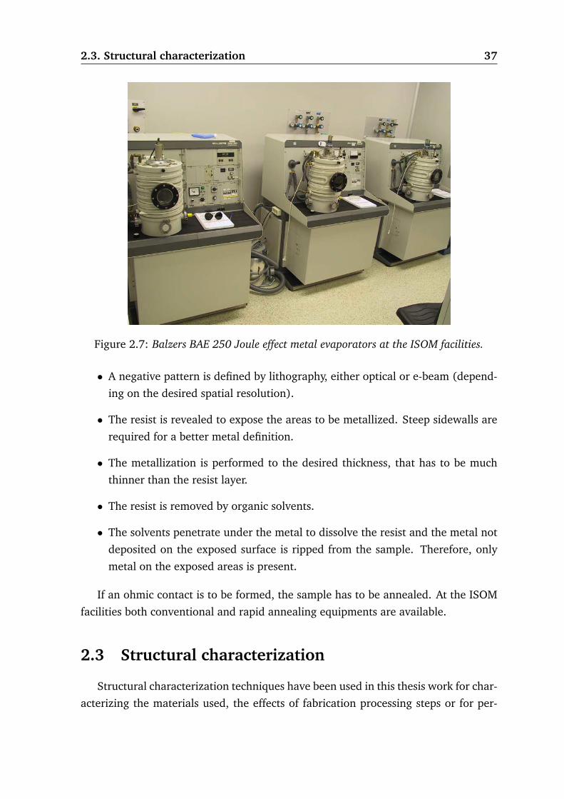
2.3. Structural characterization 37
Figure 2.7: Balzers BAE 250 Joule effect metal evaporators at the ISOM facilities.
• A negative pattern is defined by lithography, either optical or e-beam (depend-
ing on the desired spatial resolution).
• The resist is revealed to expose the areas to be metallized. Steep sidewalls are
required for a better metal definition.
• The metallization is performed to the desired thickness, that has to be much
thinner than the resist layer.
• The resist is removed by organic solvents.
• The solvents penetrate under the metal to dissolve the resist and the metal not
deposited on the exposed surface is ripped from the sample. Therefore, only
metal on the exposed areas is present.
If an ohmic contact is to be formed, the sample has to be annealed. At the ISOM
facilities both conventional and rapid annealing equipments are available.
2.3 Structural characterization
Structural characterization techniques have been used in this thesis work for char-
acterizing the materials used, the effects of fabrication processing steps or for per-

38 Chapter 2. Design, fabrication and experimental techniques
forming measurements on fabricated devices. This section describes the usual prin-
ciples of the structural characterization techniques that have been employed. Mod-
ifications of these techniques for performing more sophisticated measurements for
device characterization are later described, in sections 2.6 and 2.6.3.
2.3.1 X-ray diffraction
This characterization technique allows a fast and non destructive measurement
of the parameters of a crystalline material. The simplest description of the X-ray
diffraction technique is based on the Bragg observations [90]. An X-ray beam that is
focused on the surface of a three-dimensional crystal lattice will be diffracted when
the impinging angle satisfies the Bragg condition:
nλ = 2d sin θB (2.3)
where n is the diffraction order, d is the distance between the diffracting atom
layers, λ is the beam wavelength and θB the impinging angle (Bragg angle).
In order to obtain a constructive interference (2.3) has to be satisfied. The diffrac-
tometer varies the impinging angle recording the diffraction peaks that appear at the
detector. The full width at half maximum (FWHM) is a measurement of the crys-
talline quality of the sample and is influenced by the spectral and angular divergence
of the X-ray beam.
Diffractometer used in this thesis
For the analysis discussed in this thesis a D3 Bede Scientific diffractometer was
used, located at the ISOM facilities. It is composed of the following components:
• X-ray tube. A copper C-Tech tube is used as X-ray source.
• Primary optics. It is a monochromator that eliminates all the spectral lines
except the copper Kα1 line (λ = 1.54056 Å).
• Sample holder. It has a set of goniometers that allow the alignment of the
sample with the beam.
• Detector. It also has a goniometer for correcting the alignment.
The primary optics, sample holder and detector are allowed to rotate in order
to perform various type of measurements. A system for adding slits to the beam

2.3. Structural characterization 39
Figure 2.8: D3 Bede Scientific X-ray diffractometer used in this work.
path is also available. Slits from 0.5 mm to 5 mm may be added to the source, for
adjusting the beam section to the sample size, or to the detector, for filtering noise
and improving resolution.
Measurement types
Basically two types of measurements have been performed using the high resolu-
tion X-ray diffraction (HRXRD) equipment.
• Rocking curves. This configuration fixes the source and detector angles to a
maximum diffraction angle. The sample is rotated around the maximum posi-
tion in order to assess the dispersion in the orientation of the diffracting planes.
The figure of merit is the FWHM of the obtained peak, which provides infor-
mation about the crystal quality. The narrower the reflection is, the better
alignment of parallel planes, so low mosaicity of the crystal leads to narrow
peaks in rocking curves.
• θ/2θ curves. The sample and source are rotated to change the impinging angle.
The different reflections determine the Bragg angle of the crystal planes. The
beam at the detector is usually filtered using a slit in order to better separate
the diffraction peaks. The position of the peaks provide information about

40 Chapter 2. Design, fabrication and experimental techniques
crystal composition and residual strain deforming the lattice. If the detector
is fully opened information about mosaicity can also be extracted (this scan is
also referred as ω/2θ), but the reflection peaks must be sufficiently separated
to avoid overlapping.
Measurement analysis
Performing the two types of scans information about crystal quality, composition
and residual strain can be extracted. The theory of X-ray diffractometry is well es-
tablished and can be found at [91]. In this thesis the measured diffractograms were
analyzed with a simulation software that was used to fit the peaks and extract the
desired information. The software is based on a dynamic diffraction model following
the Takagi-Taupin formalism. It uses exact parameters in order to avoid errors when
working with large lattice parameters, such as those for nitrides [92].
2.3.2 Scanning electron microscopy
The scanning electron microscope images shown in this thesis report have been
obtained with various instruments. However, the majority of the SEM analysis was
performed using the JEOL 5800 SM microscope located at the ISOM facilities.
The SEM instrument uses electrons that are emitted from a filament and colli-
mated to for a beam. The beam is accelerated to typical energies of 20 − 40 KeV .
This beam is focused on the sample and used to scan the surface. The electron-
matter interaction produces the emission of secondary electrons from the sample
that are collected to form the image. The amount of the secondary electrons emitted
depends on the material that is being illuminated, providing contrast for the different
materials in the sample.
As a drawback, the sample has to be conductive, either intrinsically or with the
aid of a metallization. Otherwise, the electron accumulate on the surface and deflect
the beam, blurring the image or even preventing an image to be formed.
The samples were scanned either in plan view mode with the surface aligned per-
pendicular to the beam or in lateral view mode with tilted samples. The variation of
the view angle allows the characterization of the surface, structures or even thickness
of the samples. Therefore, the SEM technique provides a versatile means of imaging
analysis of the materials and structures produced in this thesis.

2.3. Structural characterization 41
Figure 2.9: JEOL scanning electron microscope used in this work.
2.3.3 Atomic force microscopy
The atomic force microscopy (AFM) is a precise surface characterization tech-
nique, which is used to acquire high resolution topographic images of the surface of
a sample. There are several operation modes, among which the most important are
the contact mode and the tapping mode.
The tapping mode has been used in this work for topographic imaging. The
operation principle relies on the interaction of a vibrating tip and a surface in close
proximity. The AFM drives a cantilever close to its resonant frequency and sets an
operation amplitude. The amplitude of the vibration is measured on a four segment
photodiode by means of the reflex of a laser spot directed to the tip’s end. When
the tip approaches the surface the amplitude is modified and the microscope will
control to maintain the vibration amplitude constant, using a feedback loop. The
amplitude is controlled moving the sample in the vertical direction by means of a
piezoelectric actuator. Therefore, as the sample is scanned, the control loop will force
the sample to move upwards and downwards in order to maintain the tip’s vibration
constant. This movement is controlled by the voltage applied to the piezoelectric
holder where the sample is mounted. Consequently, the control signal is a very
precise representation of the surface under study.
The tapping mode has been used due to certain advantages, namely

42 Chapter 2. Design, fabrication and experimental techniques
Figure 2.10: Nanoscope atomic force microscope used in this work.
1. High lateral resolution (ranging from 1 nm to 5 − nm depending on the scan
size and speed).
2. Low contact force, leading to low surface damage.
3. Virtually zero lateral forces and interactions, producing no scratching on the
scanned surfaces.
Nevertheless, this technique is slow and requires a deep expertise in order to
produce an artifact free image. The AFM microscope which was used for most of the
measurements for this thesis was a Digital Instruments Nanoscope IIIa located in the
ISOM facilities.
2.3.4 White light interferometry
White light interferometry is a technique that uses a phase shifting interferometer
combined with an optical microscope to provide a non-contact 3D method for mea-
suring roughness and feature morphology on the sample surface. This technique is
able to rapidly measure features on large areas form the sub-nanometer to the mi-
cron scale. An Ambios Xi-100 interferometer, located at the ISOM facilities, was used
in this thesis for characterizing the deformations of free-standing structures.
Measurement principle
The measurement is based in viewing the optical path difference between a sam-
ple beam and a reference beam. The beam undergoes constructive and destructive
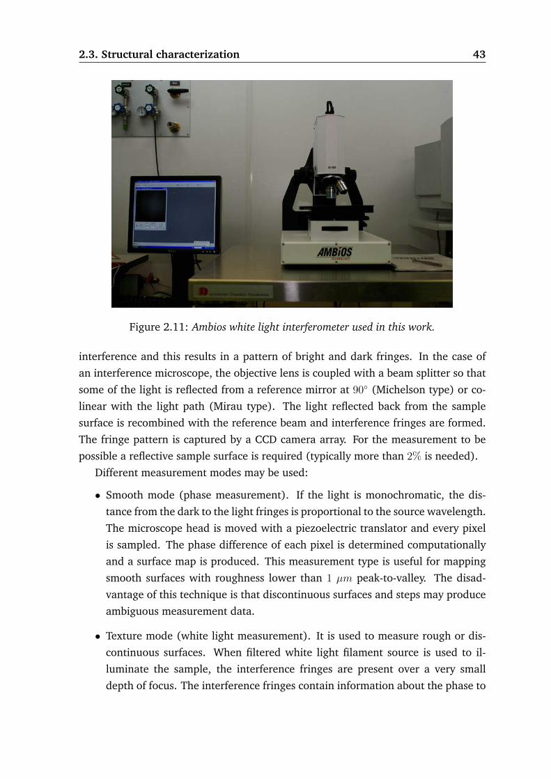
2.3. Structural characterization 43
Figure 2.11: Ambios white light interferometer used in this work.
interference and this results in a pattern of bright and dark fringes. In the case of
an interference microscope, the objective lens is coupled with a beam splitter so that
some of the light is reflected from a reference mirror at 90 (Michelson type) or co-
linear with the light path (Mirau type). The light reflected back from the sample
surface is recombined with the reference beam and interference fringes are formed.
The fringe pattern is captured by a CCD camera array. For the measurement to be
possible a reflective sample surface is required (typically more than 2% is needed).
Different measurement modes may be used:
• Smooth mode (phase measurement). If the light is monochromatic, the dis-
tance from the dark to the light fringes is proportional to the source wavelength.
The microscope head is moved with a piezoelectric translator and every pixel
is sampled. The phase difference of each pixel is determined computationally
and a surface map is produced. This measurement type is useful for mapping
smooth surfaces with roughness lower than 1 µm peak-to-valley. The disad-
vantage of this technique is that discontinuous surfaces and steps may produce
ambiguous measurement data.
• Texture mode (white light measurement). It is used to measure rough or dis-
continuous surfaces. When filtered white light filament source is used to il-
luminate the sample, the interference fringes are present over a very small
depth of focus. The interference fringes contain information about the phase to

44 Chapter 2. Design, fabrication and experimental techniques
< 1 nm and also have unique assignment of fringe count. The microscope head
is scanned vertically through the surface focal point and the resulting camera
images are stored as a series of frames. Vertical ranges beyond microscope
focus can be measured with this technique (up to 100 µm).
2.4 Optical characterization
Material quality is fundamental for achieving good electronic and mechanic per-
formance. For semiconductors a very fast and accurate manner of determining ma-
terial properties is through optical characterization. There are various techniques
suitable for this purpose, and describing them deeply falls out of the scope and objec-
tives of the present work. Nevertheless, the fundamental aspects of the main optical
techniques that have been employed in this thesis will be presented in the following
paragraphs.
2.4.1 Photoluminescence
This technique has been used for studying good quality crystalline semiconductor
materials. The sample is illuminated with a monochromatic source, normally a laser,
with a wavelength sufficiently short to be absorbed by the material under study and
generate electron-hole pairs. These pairs will eventually recombine after reaching
thermal equilibrium, and photons will be generated, whith a wavelength that is a
fingerprint of the energy levels present in the material. Studying the emitting energy
levels, the width of their emission lines and the variation of their energy with temper-
ature and illumination power, valuable information may be obtained. For material
with sufficient quality and under low temperature conditions, the electron-hole pairs
tend to form free excitons. The recombination of an exciton leads to the emission of
a photon with energy equal to
EFX = Eg − Eb (2.4)
where Eg is the bandgap energy and Eb is the exciton binding energy. Therefore, the
variation of the energy of the exciton (EFX) follows that of the bandgap and it may
be adjusted to a Varshni model [93,94]:
Eg = Eg(0)− σ · T 2
θ + T(2.5)

2.4. Optical characterization 45
where Eg(0) is the bandgap at 0K, θ is the Debye temperature and σ is a fitting
parameter.
Also, the excitons may become localized near an impurity site. These fixed exci-
tons have a localization energy (ELD or ELA) related with the ionization energy of
the donor (ED) or acceptor (EA) to which they are fixed, using the Haynes rule [95]
it could be written:
ELD = EFX − EDX = (0.2)ED → donors
ELA = EFX − EAX = (0.1)EA → acceptors(2.6)
where the energies EDX and EAX are the associated photoluminescence (PL)
lines with the fixed exciton transition. Combining with the above expressions it is
immediate to find that the behavior with the temperature is equal to that for the
gap until kT approaches the localization energy of the exciton, which then becomes
delocalized and behaves as a free exciton.
Other allowed transition is the recombination from a band edge to an impurity
level. This may happen when a free electron falls to an ionized acceptor site (e− A)
or when a hole recombines with an ionized donor site (h − D). In this case the
transition is given by
Ee−A = Eg − EA + kT2
Eh−D = Eg − ED + kT2
(2.7)
where the term kT2
represents the kinetic energy of the free carrier. For high
temperature the variation with the temperature is that as for the bandgap. However,
at low temperature, the kinetic energy term is dominant.
Finally, transitions between donor and acceptor energy levels (D − A) is also
observable [94]. In this case the transition energy is given by
EDA = Eg − ED − EA +q2
4πεr(2.8)
where r is the distance between impurity sites, ε is the electrical permittivity
of the material and, therefore, the last term accounts on the Coulomb attraction
energy between the ionized donors. For this type of emission a ripple is observable
because the electrically active impurities may only be placed at lattice sites. When
the temperature increases, the donors become ionized and the electron population
rises, shielding the distant electron hole pairs. Therefore, the Coulomb attraction
term becomes dominant and the emission energy shifts to higher values when the
temperature is further increased.
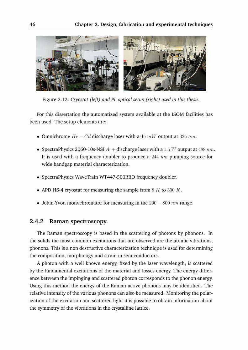
46 Chapter 2. Design, fabrication and experimental techniques
Figure 2.12: Cryostat (left) and PL optical setup (right) used in this thesis.
For this dissertation the automatized system available at the ISOM facilities has
been used. The setup elements are:
• Omnichrome He− Cd discharge laser with a 45 mW output at 325 nm.
• SpectraPhysics 2060-10s-NSIAr+ discharge laser with a 1.5W output at 488 nm.
It is used with a frequency doubler to produce a 244 nm pumping source for
wide bandgap material characterization.
• SpectraPhysics WaveTrain WT447-500BBO frequency doubler.
• APD HS-4 cryostat for measuring the sample from 8 K to 300 K.
• Jobin-Yvon monochromator for measuring in the 200− 800 nm range.
2.4.2 Raman spectroscopy
The Raman spectroscopy is based in the scattering of photons by phonons. In
the solids the most common excitations that are observed are the atomic vibrations,
phonons. This is a non destructive characterization technique is used for determining
the composition, morphology and strain in semiconductors.
A photon with a well known energy, fixed by the laser wavelength, is scattered
by the fundamental excitations of the material and losses energy. The energy differ-
ence between the impinging and scattered photon corresponds to the phonon energy.
Using this method the energy of the Raman active phonons may be identified. The
relative intensity of the various phonons can also be measured. Monitoring the polar-
ization of the excitation and scattered light it is possible to obtain information about
the symmetry of the vibrations in the crystalline lattice.

2.4. Optical characterization 47
The experimental setup is composed of a monochromatic laser for the excitation,
a illumination system for focusing the spot on the sample, a photodetector and a
spectrometer for measuring the scattered spectrum. The Raman measurements pre-
sented in this thesis were performed at the facilities of the Instituto de Ciencias de
Materiales de Madrid (ICMM) of the Consejo Superior de Investigaciones Científicas
(CSIC).
2.4.3 Fourier transform infrared spectroscopy
The Fourier transform infrared (FTIR) spectroscopy technique is used for the char-
acterization of thin layers. It is based on the absorption of photons by the vibration
modes of the atomic bonds in the material. The absorption is produced at deter-
mined wavelengths in the middle infrared spectrum range. The absorption peaks
reveal information about the structure and composition of the material.
The measurement equipment has a Michelson interferometer with a mobile mir-
ror and a wide band infrared source. The light is splited and reflected by a fixed and
a mobile mirror. The reflected beams are recombined and are passed through the
sample under measurement. The interfering beams are collected by a detector which
registers the intensity for a given mirror displacement. The registered interferogram
is converted to the frequency domain by a Fourier transform and the absorption peaks
versus illumination wavelength are obtained.
Figure 2.13: Nicolet FTIR instrument used in this thesis.

48 Chapter 2. Design, fabrication and experimental techniques
For normalizing the measurement and eliminating the substrate contribution,
measurements without sample and with a substrate reference sample have to be
performed. The collected spectra are used to calibrate the measurement and extract
the thin layer contribution to the absorption spectrum.
In this thesis a Nicolet 5-PC FTIR instrument, located at the ISOM facilities,
was used to characterize AlN thin layers deposited on Si(001) in the 400 cm−1 to
4000 cm−1 range.
2.5 Electrical characterization
Electrical characterization techniques were also used in this thesis, using the
equipment available at the ISOM facilities. The techniques used were very direct
and no deep explanation is needed. In this section the equipment used for this dis-
sertation is described.
2.5.1 Current-voltage curves
The measurement of the current-voltage characteristic of a structure is used to
reveal several properties:
• Layer electrical resistance.
• Loss currents as a function of polarization voltages.
• Breakdown fields. Measured as the field for which the current shows a very
high increase.
The measurement setup is very simple. A structure is fabricated with metal pads
that are contacted with probes. A voltage is supplied and the current flowing through
a given pair of contacts is measured.
2.5.2 Capacitance-voltage curves
This measurements are similar to the current-voltage characteristics with the par-
ticularity that capacitance is measured instead of current. The capacitance changes
and hysteresis reveal the amount of free carriers, trapped charges, depletion layers
and other electrical characteristics of thin layers.
Interfaces between semiconductors can also be analyzed. The accumulation, de-
pletion and inversion regions can be modified by applying voltages to the contacts.

2.6. Electromechanical characterization 49
The voltages limiting these regions are determined and provide a useful tool for the
material characterization.
2.5.3 Characterization equipment
For the measurements standard equipment was used:
• Parameter analizer, used for measuring I-V characteristics.
• Capacitometer, used for the determination of C-V curves.
• Probing station, used to contact structures directly on chip by means of probing
needles.
• Mercury probe. This probe is used to form a Schottky contact on a semicon-
ductor surface without the need of metallizing the sample. The back of the
substrate has to be metallized in order to be contacted by a standard contact so
the complete stack can be polarized vertically.
2.6 Electromechanical characterization
Special characterization techniques for mechanically characterizing free-standing
microstructures have been used. These techniques, although not new, have been
adjusted in this thesis for the measurement of the developed MEMS. In fact, this
task required a significant amount of time for adjusting and calibrating the required
equipment.
2.6.1 Beam deflection
The beam deflection technique is used for statically characterize free-standing
structures and determine the elastic modulus. The principle is simple, the structure
is point loaded at a certain point and the deflection is measured. The deflections
obtained applying the load on different points is fitted to a theoretical curve for the
structure under study and the mechanical parameters are obtained.
Instrumental setup
Microbeam structures were statically characterized using a Veeco Multimode AFM
with a Nanoscope IIIa controller at the ISOM facilities. Both standard piezoelectric

50 Chapter 2. Design, fabrication and experimental techniques
and an nPoint position controller scanner were employed. Veeco rectangular silicon
RTESP7 and diamond-like-carbon coated TESPD probing tips were used for loading
the structures under measurement. The microbeams were loaded by pressing with
the AFM cantilever tip at different points. Force-separation curves were recorded in
order to extract the spring constant for different loading points. In order to ensure
a correct spring constant value, the AFM cantilever tip has to be driven from out of
contact position to deflection due to contact for each probing point.
The procedure is very reliable as the results obtained for all combinations of scan-
ner and AFM tip were very similar, with a dispersion lower than 5%. In order to
extract the effective string constant a calibration of the setup has to be performed for
every measurement. The calibration process consists in recording the force separa-
tion curve while pressing the AFM cantilever tip on a solid surface. The calibration
curve is associated to the cantilever tip spring constant and is used to extract the
effective spring constant of the loading points on the free-standing structure. The
method is depicted in figure 2.14.
Figure 2.14: Measurement principle of the beam deflection curves with AFM loading.
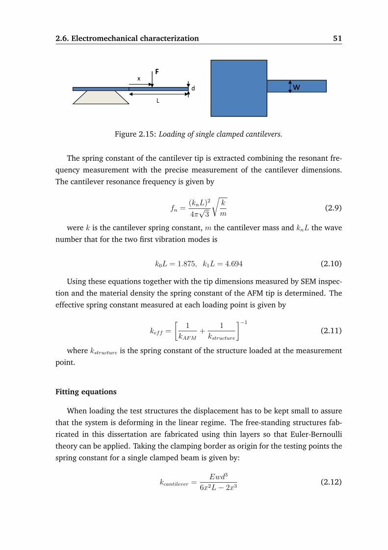
2.6. Electromechanical characterization 51
Figure 2.15: Loading of single clamped cantilevers.
The spring constant of the cantilever tip is extracted combining the resonant fre-
quency measurement with the precise measurement of the cantilever dimensions.
The cantilever resonance frequency is given by
fn =(knL)2
4π√
3
√k
m(2.9)
were k is the cantilever spring constant, m the cantilever mass and knL the wave
number that for the two first vibration modes is
k0L = 1.875, k1L = 4.694 (2.10)
Using these equations together with the tip dimensions measured by SEM inspec-
tion and the material density the spring constant of the AFM tip is determined. The
effective spring constant measured at each loading point is given by
keff =
[1
kAFM+
1
kstructure
]−1(2.11)
where kstructure is the spring constant of the structure loaded at the measurement
point.
Fitting equations
When loading the test structures the displacement has to be kept small to assure
that the system is deforming in the linear regime. The free-standing structures fab-
ricated in this dissertation are fabricated using thin layers so that Euler-Bernoulli
theory can be applied. Taking the clamping border as origin for the testing points the
spring constant for a single clamped beam is given by:
kcantilever =Ewd3
6x2L− 2x3(2.12)

52 Chapter 2. Design, fabrication and experimental techniques
where E is the material Young’s modulus, w the cantilever width, L the cantilever,
d the cantilever thickness and x the loading point, as depicted in figure 2.15. Double
clamped beams can be also characterized by this technique. Nevertheless, measuring
these structures by this technique is difficult as they are much stiffer than the probing
tip, so the achieved deformations are smaller than for cantilevers. Besides, if residual
tensile stress is present in the structure an additional stiffening is produced. However,
for measuring a double clamped beam without residual stress the following equation
has been used:
kbeam =L2Ewd3
6x3(L− x)2(1− L−2x3L
)(2.13)
Combining (2.12) and (2.13) with (2.11) the equations used to fit the measure-
ments are obtained.
2.6.2 Magnetomotive spectroscopy
The magnetomotive spectroscopy consists of a setup used for determining the
resonance frequencies of free-standing structures. A structure is placed in a vacuum
chamber and a magnetic field is applied in the same plane of the structure. A current
is injected to flow through the structure perpendicularly to the applied magnetic
field. This produces a Lorentz force in the vertical direction. Therefore, the sample
is uniformly loaded perpendicularly to the structure plane.
If the injected current frequency equals an out-of-plane resonance mode fre-
quency a large vibration will be induced on the structure. The out-of-plane defor-
mation produces an induced voltage that can be approximated by:
Vind ∝1√Eρ· L
3
wd2iB2 (2.14)
where i is the injected current and B the applied magnetic field. The induced
voltage originates a reflection in the excitation signal that can be measured by a
network analyzer.
The setup used in this thesis is composed of:
• Network analyzer. Equipment used for driving the structures and measuring
the induced reflections. The measurement range is from 10 Hz to 1 GHz.
• Network impedance adapter. Used to adapt the impedance in order to sup-
press the artifacts induced in the radio frequency measurement due to spurious
reflections and maximize the signal generated by the beam vibration.

2.6. Electromechanical characterization 53
• Coplanar radiofrequency probes. Used to drive and measure the vibrating struc-
tures.
• Vacuum chamber. Used to measure the vibrating structures at different ambient
pressures.
• Permanent magnet. A permanent magnet setup was used to apply a 0.5 T
magnetic field on the sample plane.
The restrictions of this technique is that the sample has to be conductive, so metal-
lization of the structure is required and that the current has to cross the free standing
Figure 2.16: Magnetomotive setup used in this work.

54 Chapter 2. Design, fabrication and experimental techniques
structure. Thus, only double clamped structures can be measured by this technique,
as cantilevers lack a second contact to close the current path.
2.6.3 Piezoresponse characterization
The piezoelectric coefficient determination of the material is required for the de-
vice simulation. A technique for the accurate determination of the vertical piezoelec-
tric coefficient has been calibrated as part of this dissertation. The equipment was
located at the facilities of the IAF at Freiburg, and the measurement instrument was
calibrated when the candidate was working under Dr. V. Lebedev and Dr. V. Cimalla
supervision, although it was later reproduced at the ISOM facilities.
The measurement principle is simple. A piezoelectric material is contacted from
the bottom and top surfaces by means of metallization patterns. The structure is
placed in an AFM setup with a Nanoscope IIIa controller. The AFM tip is driven
into static contact with the surface. A voltage applied to the electrodes will induce
a deformation that will deflect the AFM tip, displacing the laser reflection on the
detector [96–99].
The detector output voltage has to be accessed and connected to a low noise
lock-in amplifier. The driving signal is tuned to the amplifier lock frequency and
the detector signal amplitude is measured for different excitation amplitudes. The
relation between the measured and applied amplitudes is linear and proportional to
the d33 piezoelectric coefficient. The proportion coefficient is obtained by measuring
Figure 2.17: Piezoresponse measurement setup used in this thesis.
2.6. Electromechanical characterization 55
a reference sample with a well known piezoelectric coefficient. The setup has been
schematically represented at figure 2.17.
This technique provides an easy and reliable characterization of the d33 param-
eter. Nevertheless, the vibration induced on the sample has an amplitude in the
subnanometer range. Therefore, accurate calibration and noise filtering is required
in order to suppress the distortions that affect the measurement. With accurate han-
dling good determination of the piezoelectric coefficients have been obtained.
Reference measurements
For a correct interpretation of the measurements it is of utmost importance to
calibrate with a known standard before every measurement session. In this manner
all the variations due to geometry changes, temperature drift or piezoelectric scanner
creep are taken into account, and error sources are minimized. For this dissertation
LiNbO3 standards have been used. This is because it is a relatively cheap piezo-
electric material with a good long term stability and with piezoelectric constants
accurately determined by the cut. The LiNbO3 is material which forms a trigonal
crystal lattice with threefold symmetry. It belongs to the 3m or C6v point group, and
therefore, has four piezoelectric coefficients defining the [d] matrix as 0 0 0 0 d15 −d22−d22 d22 0 d15 0 0
d31 d31 d33 0 0 0
(2.15)
In order to evaluate the longitudinal component of [d] normal to different oriented
surfaces a transformation has to be made. This transformation is a counterclockwise
rotation with angle φ around Z and a clockwise rotation θ around the new X ′ axis in
the following manner
[d′′] = [Ax][Az][d][Nz]T [Nx]
T (2.16)
The new [d′′] matrix will contain the piezoelectric coefficients in various orienta-
tions (cuts of the crystal). We are interested in the d′′33(φ, θ) coefficient, which is the
one which is directly measurable by the piezoresponse technique. Using (2.17) and
(2.18), a general expression may be given to d′′33 as follows

56 Chapter 2. Design, fabrication and experimental techniques
[Az]
=
cos(φ
)si
n(φ
)0
−si
n(φ
)co
s(φ
)0
00
1
[Nz]
=
cos2
(φ)
sin2(φ
)0
00
cos(φ
)·s
in(φ
)
sin2(φ
)co
s2(φ
)0
00
−co
s(φ
)·s
in(φ
)
00
10
00
00
0co
s(φ
)−
sin(φ
)0
00
0si
n(φ
)co
s(φ
)0
−2·c
os(φ
)·s
in(φ
)2·c
os(φ
)·s
in(φ
)0
00
cos2
(φ)−
sin2(φ
)
(2.1
7)
[Ax]
=
10
0
0co
s(θ)−
sin(θ
)
0si
n(θ
)co
s(θ)
[Nx]
=
10
00
00
0co
s2(θ
)si
n2(θ
)−
cos(θ)·s
in(θ
)0
0
0si
n2(θ
)co
s2(θ
)co
s(θ)·s
in(θ
)0
0
02·c
os(θ
)·s
in(θ
)−
2·c
os(θ
)·s
in(θ
)co
s2(θ
)−
sin2(θ
)0
0
00
00
cos(θ)
sin(θ
)
00
00
−si
n(θ
)co
s(θ)
(2.1
8)
d′′ 33
=d33·c
os(θ
)3+d22·(
cos2
(φ)−
2·c
os(φ
)·s
in2(φ
))·s
in3(θ
)+
(d15
+d31)·s
in2(θ
)·c
os(θ
)(2
.19)

2.6. Electromechanical characterization 57
Figure 2.18: Piezoelectric normal response (d′′33) of LiNbO3. The 3D response has beenplotted (up) together with the cut for the cut for xz plane (down, left) and yz plane(down, right).
From this equation and taking into account the values of the piezoelectric coeffi-
cients after Warner et al. [100] the value of d′′33 for the commercial available orienta-
tions have been calculated.
The general normal piezoresponse of LiNbO3 has a characteristic double sad-
dle shape as depicted in figure 2.18. It is observed that this material has a strong
anisotropic piezoelectric response with directions that have a very strong response
and other for which no response exists. For the experiments performed in this dis-
sertation the Y + 128o cut was used due the its large piezoresponse, long term time
stability and because its a common commercial available substrate.
With the used set-up stable calibration measurements were performed as shown
in figure 2.19. A nice linear fit is observable, providing accurate and reliable slope
Parameter d15 d22 d31 d33Value (pm/V ) 68 21 −1 6.2
Table 2.1: Piezoelectric constants for LiNbO3, as from Warner et al. [100].

58 Chapter 2. Design, fabrication and experimental techniques
Cut d′′33 (pm/V )X axis 0Z axis 6.2Y axis 21.0
Y axis + 41o 35.82Y axis + 64o 17.85Y axis + 128o 18.15Y axis + 163o 0.3
Table 2.2: Piezoelectric d33 response for LiNbO3 for different cuts.
parameter that defines the relation between the measured millivolt amplitude and
the induced picometer vibration. This relation allows the determination of the vi-
bration amplitude of a sample for a given excitation and, therefore, calculating the
piezoelectric parameter of the layer under test.
2.6.4 Determination of piezoelectric properties of thin films
This measurement method has been used for the determination of the piezoelec-
tric properties of thin AlN films over a foreign substrate. As described at [101,102]
the boundary conditioins imposed on the film film grown on a substrate impose a
clamping of one side of the film. The effect is that the value measured is not directly
that of d33 but d33eff , given by:
d33eff = d33 + 2
(d31s
E13
sE11 + sE12
)(2.20)
where d31 ≈ −d33eff/2 for AlN and sEij are the terms of the elastic compliance
matrix, that can be taken from [103].
Figure 2.19: Calibration curves corresponding to a reference LiNbO3 sample.

Part II
Manufacturing and material issues
59

Chapter 3
Dry etching of functional materials
The first technological step that has to be optimized is the pattern transfer to the
functional materials. The processing of functional materials for MEMS devices has
the peculiarity that deep etchings have to be performed. The complete thickness
of the layer has to be removed, so large anisotropic etch rates are required. Low
damage and selectivity to sacrificial layer are also desired, so the technology is more
controllable. The variety of material used in this dissertation and the low maturity of
bulk processing techniques for them, led to make the optimization of the dry etching
technology the starting point for this thesis.
In this chapter the results for the optimization of several etching procedures are
presented. Etching rates, anisotropy and surface morphologies of the materials used
in this thesis have been deeply studied and optimized. The results and discussion
include considerations of the possible usage of the employed materials, either as
functional material or sacrificial layers. The etching of sacrificial layers for releasing
free-standing structures is presented in chapter 4.
Reactive ion etching (RIE) with SiCl4 : Ar : SF6 gas mixtures have been studied
for:
• GaN . Basic material of the III-N system and candidate for structural material
for MEMS sensors.
• AlN . This material can be used as sacrificial layer or a piezoelectric functional
material for MEMS structures.
• InN . Third main binary semiconductor of the III-N system that can be used for
sensor fabrication.
• AlInN lattice matched to GaN . This ternary alloy is a good candidate for
sacrificial layer for the fabrication of relaxed GaN free-standing structures.
61

62 Chapter 3. Dry etching of functional materials
Additionally, RIE etching with H2 : O2 gas mixtures were used for:
• Nanocrystalline diamond, NCD. Used as structural material for MEMS due to
its outstanding mechanical properties.
3.1 Dry etching of GaN
As a first approach to the dry etching of nitrides, GaN dry etching was studied.
The aim of the technological optimization is to achieve a clean etching with smooth
and vertical sidewalls at the highest possible etch rate. GaN is the main functional
material of the nitride semiconductor system and it is intended to be etched to form
the functional structures of the MEMS devices. Thus, high selectivity with the sacri-
ficial layer is pursued in order to use the later layer as an etch stop.
GaN samples grown on sapphire by MOCVD were used for the dry etching opti-
mization study. The RIE reactor described in chapter 2 was used and the following
gases were employed:
• SiCl4 as the main etching reactant
• SF6 as a secondary reactant used to enhance the etch rate
• Ar for plasma stabilization
3.1.1 Preliminary trials
Pressure, flow and discharge power (PRF ) were varied for fixing the autopolar-
ization voltage of the plasma (VDC). As a first step, preliminary etches using SiCl4plasma were performed in order to identify the limitations of the equipment and pro-
vide a starting point for the study of the etch process. The resulting etch rates are
shown in table 3.1.
From the table 3.1 it is concluded that the etch rate is linear, so the influence of
the native oxide layer is negligible. The etch rate is low and increases with pressure,
Chamber pressure t = 5′ t = 10′ t = 20′ < vSiCl4 >10 mtorr 6.6 nm/min 5.5 nm/min 6.2 nm/min 6.1 nm/min20 mtorr 8.5 nm/min 8.0 nm/min 8.3 nm/min 8.3 nm/min
Table 3.1: Etch rate of GaN layers with low pressure SiCl4 plasma.

3.1. Dry etching of GaN 63
which suggest that the process is in the reaction limited regime. The preliminary
results also showed that for stabilizing the plasma the addition of Ar was required, as
it significantly improved the etching uniformity. Also, the pressure has to be increased
in order to achieve a more efficient reaction.
3.1.2 Etch rate optimization
For improving the preliminary results in terms of uniformity Ar was added to the
gas mixture. As suggested by Feng et al. [104] the addition of fluorine chemistry
to the chlorine gas should increase the etch rate. Actually, Karouta et al. [105, 106]
claim a fourfold etch rate increase when adding SF6 to an SiCl4 : Ar plasma using
a RIE reactor, achieving a maximum etch rate of 150 nm/min and a smooth etched
surface. The explanation of this effect is that the SF6 reacts with the nitrogen planes
found along the GaN c-axis to form NF3 which is a much more volatile molecule
than NCl3 [107]. Nevertheless, GaF3 might also be formed, which is difficult to
remove, therefore a trade-off between the formation of both compounds is expected
to be observed. On the whole, SF6 was added to a SiCl4 : Ar (1:1) mixture with a
flux proportion up to 40%. The fluxes of SiCl4 and Ar were kept constant to 15 sccm.
The reference etch rates without SF6 are showed in table 3.2 for several pressures
and polarization voltages. At the higher pressures, the plasma was not stable for the
higher voltages used, therefore the etch rates were not measured. Although the
etching is reaction limited and the rate increases with the chamber pressure, the
marginal increase when changing from 40 mtorr to 60 mtorr was much lower than
when increasing from 20 mtorr to 40 mtorr. A severe increase in the etch rate is
also observed when increasing VDC from 350 V to 400 V , which could indicate that
physical etching mechanisms are activated at these polarization voltages. Conversely,
etch rate has been measured to be constant with time, so no effect of native oxide
has been observed.
The addition of SF6 to the gas mixture led to an etch rate increase, as seen in
figure 3.2. Proportion of SF6 higher than 30% led, under certain etch conditions,
Chamber pressure VDC = 300 V VDC = 350 V VDC = 400 V20 mtorr 8.0 nm/min – 17.1 nm/min40 mtorr 19.1 nm/min 20.0 nm/min 34.8 nm/min60 mtorr 23.1 nm/min – –
Table 3.2: Etch rate of GaN with SiCl4 : Ar plasmas.

64 Chapter 3. Dry etching of functional materials
Figure 3.1: Constant etch rate for GaN reactive ion etching.
to difficulties in stabilizing the plasma. Thus, only proportions up to 30% are reli-
able, results with higher SF6 proportions are included in figure 3.2 only for those
conditions were reproducible etching processes were achieved.
It has been observed that a significant increase may be obtained if SF6 is added to
the gas mixture, achieving a maximum etch rate of 80 nm/min. The SF6 proportion
that optimizes the etch rate is between 25% and 30%, being the exact proportion
only dependent of the chamber pressure. The saturation of the etch rate increase
is due to the trade off in the formation of easy to etch NF3 and difficult to remove
GaF3. Moreover, if SF6 in proportions greater than 20% is added to the gas mixture
Figure 3.2: Etch rate of GaN in SiCl4 : Ar : SF6 plasmas.

3.1. Dry etching of GaN 65
a drop in the etch rate during the first minutes of etching has been observed. This
effect is attributed to the formation of GaF3 on the Ga face of the GaN which delays
the stabilization of the etching process. A similar effect has been described for other
materials [108]. This etch rate increase and saturation is a general observation for
the process, whereas the exact etch rate depends on material quality, substrate and
reactor geometry.
3.1.3 Surface morphology
The etched surface topology was studied in order to find conditions that provide
a smooth etching of the surface and sidewall. Therefore, an AFM survey has been
performed on the etched samples. It has been observed that for the etches without
SF6 the surface roughness is not modified. Conversely, addition of SF6 at proportions
higher than 20% produces a reduction of the surface roughness, if the polarization
voltage is above 300 V , see figure 3.3.
The activation of the smoothening mechanism is related to the formation of NF3
and GaF3 on the surface. The etch tends to flatten the surface for forming alterna-
tively layers of these two compounds. The smoothening of the surface appears for
concentrations of SF6 near to the optimal etch rate concentration and do not de-
pend on other parameters, as long as VDC ≥ 350 V . The surface roughness has been
measured to decrease up to a factor 8.
Another effect has been observed for the etched samples. With high chamber
pressure or high concentrations of SF6 (≥ 30%), the accumulation of droplets on the
Figure 3.3: AFM images (1 µm x 1 µm) of GaN etched without (left) and with SF6
(right), evidencing the surface smoothening.

66 Chapter 3. Dry etching of functional materials
Figure 3.4: Effect of the application of O2 plasma before the etching of GaN withSiCl4 : Ar : SF6. Samples etched under the same conditions without application of O2
plasma (left) and with the application of the cleaning plasma before the etching (right).
surface has been detected. These droplets are believed to be GaF3 that has not been
removed because they only appear with high SF6 concentration in the chamber. It
is believed that this droplets are fixed by polymerization of residues on the surface
and etch sidewalls. The etched surface cleanliness drastically improves if an oxygen
plasma is applied to burn out any polymer residues present on the exposed area, see
figure 3.4. This process has been measured not to have any influence on the etch
rate as the GaN surface oxide is etched at the same rate than the bulk material, as
discussed before.
3.1.4 Profile morphology
It has also been observed that the addition of SF6 to the plasma affected the etch
sidewall, besides of the etched surface. For etching procedures with low SF6 concen-
tration or low VDC , the obtained sidewall was vertical but rather rough. However, if
the above discussed smoothening mechanism is activated, the sidewall morphology
was also affected.
Figure 3.5: GaN dry etched with SiCl4 : Ar : SF6 with SF6 concentrations of 0% (left),10% (center) and 20% (right).

3.2. Dry etching of AlN 67
Figure 3.6: Dependence with the SF6 proportion of the GaN etched profile sidewallangle.
The transfered sidewall is smoother when the proportion of SF6 in the etching
mixture is higher. SEM images of etching profiles with various SF6 concentrations
are showed in the figure 3.5. From the pictures we conclude that the profile gets
smoother with higher SF6 concentrations. This smoothening of the transferred side-
wall has been found to depend only on the proportion of SF6 in the gas mixture.
Additionally, the transferred profile inclinations have been measured by AFM. A
strong dependence of the sidewall angle with the SF6 concentration has been found.
The modification of the inclination angle follows the same activation mechanism as
the surface smoothening. A large decrease in the measured sidewall angle has been
measured, the maximum drop was quantified to be of 20. The evolution of the side-
wall angle with the SF6 concentration has been depicted in figure 3.6. This effect
on the sidewall inclination has been first reported in this thesis work. The smoothin-
ing of the surface and sidewall is a general observation of the process, whereas the
smoothening ratio might depend on crystal quality and reactor geometry.
3.2 Dry etching of AlN
The etching of AlN was studied for two reasons, namely:
• AlN is a piezoelectric material that can be used to drive nitride or III-N/NCD
MEMS structures.
• AlN can act as sacrificial layer, as discussed in chapter 4. Therefore it may act
as stop layer for the dry etching of other III-N materials.

68 Chapter 3. Dry etching of functional materials
3.2.1 Preliminary results
AlN grown epitaxially on different substrates by different techniques was used for
the preliminary study:
• AlN grown by MOCVD on sapphire
• AlN grown by MOCVD on SiC
• AlN grown by MBE on Si(111)
The first dry etching attempts of these materials were extremely slow, with mea-
sured etch rates under 1 nm/min. Nevertheless, if the processes were maintained for
long periods the etch rate increased drastically, as shown in figure 3.7. This is because
the native oxide of AlN forms a compact layer on the sample surface that is very dif-
ficult to etch. Actually, the etching is only performed by the physical component of
the process because the reactivity of AlO3 is virtually inexistent. The thickness of the
oxide layer is variable and depends on the defect density of the material and sample
processing prior to the etching experiments.
In order to study of the etching of AlN without the effect of the native oxide layer,
a special sample of AlN was grown by MOCVD on SiC, using a 30 nm cap of GaN .
The GaN cap layer acts as a diffusion barrier in order to prevent the oxidation of the
AlN .
Figure 3.7: Effects of the native oxide on the AlN RIE etch rate.

3.2. Dry etching of AlN 69
3.2.2 Etch rate and selectivity to GaN
For the etching experiments of AlN with the GaN cap, the chamber pressure was
fixed to 40 mtorr and only VDC and the SF6 content in the SiCl4 : Ar : SF6 mixture
were varied. For all the studied etching conditions, it was observed that after etching
the first 25 nm to 30 nm, corresponding to the GaN cap, the etch rate was stable.
Thus, it may be confirmed that the GaN cap acted as a successful diffusion layer,
preventing the formation of the difficult-to-etch native oxide on the AlN layer.
Observing the etch rate plot versus SF6 concentration in figure 3.8, it is noticeable
that for concentrations of this gas lower than 20% the etch rate does not significantly
depend on VDC . This is due to the hardness of AlN , that makes this material ex-
tremely difficult to etch. For SF6 proportion of 20% the influence of VDC is much
stronger. This is explained by the physical-chemical interaction that activates the for-
mation of NF3 allowing a more efficient removal of the N planes. This effect was
already observed for the GaN samples but with a less drastic influence.
The measured etch rates are high for what is expected for AlN , which is usually
very difficult to etch, and all the studied conditions led to reproducible and uniform
results. Comparing the etch rates to those obtained for the GaN etches, it is observed
that the selectivity is maximized for SF6 proportions that enhance the etch rate of
GaN but are not sufficiently high to trigger the formation of NF3 during the etching
of AlN . At these conditions, the VDC that produces highest selectivities is 400 V as for
this plasma voltage the GaN etch rate is highly incremented and the AlN sputtering
component is still small. On the whole, an etch rate selectivity of GaN to AlN of 13
is achievable while preserving large GaN etch rates, 55 nm/min. These conditions
allow the etching of large GaN structures precisely an relying on an AlN etch stop
layer.
If higher selectivity is required, small proportions of O2 may be added to the gas
Figure 3.8: AlN etch rate (left) and selectivity to GaN (right).

70 Chapter 3. Dry etching of functional materials
mixture. Smith et al. [109] claim to have obtained selectivities as high as 50. This is
because the oxidation of GaN does not has a significant impact on the etch rate, as
opposed to the large influence showed in AlN . These observations have been con-
firmed in the experiments carried out for this dissertation. Nevertheless, the addition
of O2 might difficult the masking technology, as photoresist masks will be rapidly
etched in plasmas containing active oxygen species. Probably, this technique would
require the use of metal masks, which could difficult the production of functional
MEMS structures.
3.2.3 Surface morphology
The AlN samples could not be studied by means of scanning electron microscopy.
This is because the material exhibits strong insulating characteristics, due to the large
band gap. Thus, the sample gets rapidly charged and SEM imaging is impossible
because the impinging electron get deflected by the accumulated electrostatic charge
on the AlN surface. Consequently, only AFM survey was used for characterizing the
etched surface.
The roughness of the unetched surface has been considered to be similar to the
surface roughness of the AlN . The presence of a thin GaN cap has a negligible
influence on the surface roughness, as the growth of GaN by MOCVD has been opti-
mized. The measurements of the roughness of the etched surface was very similar to
the values measured on the original surface. No defect was induced during etching.
Conversely, the chemical polishing effect described for the GaN etching study was
not observed in the case of the RIE experiments with AlN .
Lastly, no residues were found to accumulate neither on the etched surface nor on
the pattern sidewall. This indicates that either the reaction by-products are removed
efficiently or that they form a continuous layer on the etched surface. In any case,
no influence on the resulting surface morphology was found for any of the studied
conditions.
3.3 Dry etching of InN
InN is a material with interesting properties for the manufacturing of semicon-
ductor devices for optical communications, sensors and photoelectrical applications.
Besides, it is a limit composition of the ternary (Al, In)N and (Ga, In)N compounds.
Therefore, studying the etching properties of this material is interesting for produc-

3.3. Dry etching of InN 71
Figure 3.9: SEM images of the droplet accumulation on InN surface for etches withSF6.
ing patterns on InN functional layers. For the dry etching study InN samples grown
on Si(111) by MBE have been used. For the etching experiments the pressure was
fixed to 40 mtorr and VDC and the SF6 addition were varied.
3.3.1 Residual accumulation on the etched surface
The first effect that has been observed is that the addition of SF6 to the etching
gas mixture produces droplet accumulation on the etched surface. Only for SF6
proportion of 10% and VDC ≤ 300 V clean etched surfaces were obtained. These
residuals are believed to be accumulations of a low volatile compound, likely InF3,
that forms droplets on the surface when it is produced in large quantities [110,111].
Therefore, when the amount of reactive fluorine in the chamber, either because SF6
proportion or VDC are high, InF3 is produced in excess and cannot be removed by
sputtering, forming the observed droplets, see figure 3.9.
In this case the droplet accumulation was slightly reduced if an O2 plasma inciner-
ation process was applied prior to the etch but droplets are still present on the etched
surface after the processing even using the O2 plasmas to remove organic residues.
Thus, the mechanism for droplet accumulation in the case of InN is considered to
be intrinsic to the etching with SF6 and not favored by residuals as was the case for
GaN .
3.3.2 Etch rate and selectivity to GaN
The etches performed at the conditions that do not produce droplets on the etched
surface show the following characteristics:

72 Chapter 3. Dry etching of functional materials
Figure 3.10: InN etch rate (left) and selectivity to GaN (right).
• Those performed with a SiCl4 : Ar gas mixture depend linearly with VDC . This
observation suggests that no change in the etch mechanism is produced when
changing the plasma autopolarization voltage.
• The etch rate is increased when SF6 is added to the gas mixture. This is due
to the more efficient removal of the N planes, this effect is common to all the
III-N materials. However, as discussed before, low concentrations of active F
have to be maintained in the plasma in order to avoid InF3 droplet formation.
The etch rate and selectivity to GaN are plotted in figure 3.10. In all cases, the
etch rate was constant with the etching time, indicating that no effect of the native
oxide is present. All the etching procedures exhibited an excellent uniformity and
reproducibility, providing a reliable etching technology.
The selectivity to GaN is poor and varies from 1.4 to 0.75. It has been measured
that InN is easier etched than GaN if VDC is increased. Moreover, the addition of
SF6 to the plasma lowers the etch rate compared to GaN . This etch rate lowering
is explained by the formation of InF3, which is much more difficult to remove than
GaF3.
3.3.3 Surface morphology
The etched surface was studied by SEM and AFM techniques. As was the case
for GaN no change in the surface morphology was observed for the SiCl4 : Ar gas
mixtures. The surface roughness ratio of the etched to unetched surface for this
mixture was found to be between 0.9 and 1.1, see figure 3.11.
However, the addition of SF6 to the plasma, in the conditions that did not let to
droplet formation, produced an approximate twofold surface roughness reduction.

3.4. Dry etching of AlInN lattice matched to GaN 73
Figure 3.11: SEM images of InN etched with SiCl4 : Ar : SF6 (1:1:0.1) at VDC =300 V .
This is the same effect that was discussed for the GaN etching experiments. Further
investigation of this effect is not possible as other etch conditions with SF6 produce
InF3 droplet accumulation on the etched surface.
3.4 Dry etching of AlInN lattice matched to GaN
The main issue which hinders the application of III-N materials to MEMS de-
vices is the large residual stress present at the heterojunctions. When released, the
material relieves the residual stress and the micromechanical structure is deformed,
usually by an out-of-plane buckling. The origin of this large residual stress is due to
the material growth techniques. III-N materials are grown epitaxially on substrates
which are not lattice matched to the grown material. Therefore, during growth, the
material is largely strained in order to adapt to the substrate lattice. Most of this
strain is plastically relaxed by the formation of defects in the lattice structure [112].
Nevertheless, sufficient residual stress is retained, enough to deform the microme-
chanical structures, usually in the order of hundreds of MPa [113]. Moreover, due to
the growth conditions this strain is not evenly distributed in the material and large
strain gradients usually exist along the growth direction [112]. These issues cause
the buckling of the structures when the substrate is removed, hindering the applica-
tion of III-N materials in MEMS devices [114–116].
Consequently, the need of finding a solution to this issue has led to the consider-
ation of alternative substrates or sacrificial layers. In this dissertation, thick AlInN
layers have been considered as possible solution. Selecting the molar fraction of Al
and In in the material it is possible to tune, not only the optical and electronic prop-
erties of the material, but also the mechanical characteristics. The lattice parameter

74 Chapter 3. Dry etching of functional materials
Figure 3.12: Lattice parameters and band gap energies of the three main binary mate-rials of the III-N family. It is seen that the lattice parameter of GaN is very close to thatof the Al0.83In0.17N .
may be adjusted to that of a layer of (Al,Ga)N grown on top. Figure 3.12 illustrates
the principle and shows that for obtaining AlInN layers lattice matched to GaN it is
required to grow material with an In molar fraction close to 0.17.
In this thesis, several etching techniques have been investigated using various
AlInN layers with different In molar fractions. In the following section the re-
sults for the dry etching experiments will be presented and the wet etching of the
(Al,Ga)N/AlInN heterostructures will be discussed in section 4.1.
3.4.1 Etch conditions
The dry etching experiments were performed using the Oxford Plasmalab µ80
reactive ion etching reactor available at the ISOM facilities. Different mixtures of
sulfur hexafluoride and silicon tetrachloride were employed and Ar was used for
plasma stabilization. The gas mixtures which were used are shown in table 3.3.
The rest of the etch conditions were set to the following:
• Total gas flux: 15 sccm: it is the maximum gas flux which leads to stable work-
ing conditions.
• Chamber pressure fixed at 40 mtorr, which is the pressure at which the etching
is most efficient for other III-N materials in the RIE reactor used for the study.

3.4. Dry etching of AlInN lattice matched to GaN 75
Mixture SiCl4 : Ar : SF6
A 1 : 1 : 0B 1 : 1 : 0.1C 1 : 1 : 0.2
Table 3.3: Gas mixtures employed in the AlInN RIE experiments.
As described at 3.1.
• DC bias from 300 V to 400 V , as it is the bias range which leads to the higher
etch rates but without appreciable bombardment damage.
The presented results were obtained for a sample ofAl0.83In0.17N grown by MOVPE
on sapphire and are compared to GaN reference layers grown by the same tech-
nique. The results were similar for the other studied molar fractions, which were in
the range of In molar fraction from 0.15 to 0.22. The results for the reference GaN
etching were previously discussed in section 3.1.
3.4.2 Etch rate and selectivity
The inclusion ofAr in the gas mixture makes the dry etching process of theAlInN
stable and reproducible. All the previous attempts of etching without Ar led to a very
poor homogeneity of the etching. The etching of the AlInN layer under the three
gas plasma is stable, reproducible and uniform, even for etching times exceeding 40
minutes.
The plot of the etch depth versus time reveals a strong linear dependence. There-
fore, even for an Al rich material such as Al0.83In0.17N , the influence of the native
oxide on the etch rate is negligible, contrary to what was observed for AlN layers
(see 3.2). The plot evidencing this effect is represented in figure 3.13.
The etch rate is increased when etching under larger DC bias. This dependence
is consistent with the previous observations for other III-N materials and with the
theory. Indeed, increasing the DC bias leads to an increase of the energy of the
impinging radicals and the physical sputtering component of the etching is increased
producing higher etch rates.
As observed for GaN , the addition of SF6 to the plasma leads to much higher
etch rates. This is due to the formation of NF3 at the nitrogen planes of the etched
material [105, 106], which is an extremely volatile by product. Nevertheless, if too
much SF6 is added to the plasma, the formation of AlF3 and InF3 should cause a
decrease of the etch rate. However, under the studied conditions this saturation effect

76 Chapter 3. Dry etching of functional materials
Figure 3.13: RIE etch rate under various conditions for Al0.83In0.17N layers.
was not observed indicating that the formation of NF3 is clearly dominant over the
formation of the low volatile III-F by products.
The intended application of this etching technology is for the patterning of AlInN
sacrificial layers. Therefore, a comparison of the etch rates for this material with the
etch rates of GaN is made in figure 3.14. The AlInN would be used as a sacrificial
layer beneath a functional layer of (Al,Ga)N . Thus, lower etch rates for the AlInN
are desired, in order to allow a patterning of the functional layer protecting the layers
which may be eventually beneath the MEMS structure. The etch stop is not critical
and may be tuned by controlling the etching time, therefore an etch rate ratio of 10
has been estimated as sufficient for this technology.
Figure 3.14 shows that the selectivity is maximized for plasmas without SF6,
unlike as what was observed for AlN, where a small amount of this gas improved
Figure 3.14: RIE etch selectivity of GaN to Al0.83In0.17N layers (vGaN/vAlInN).

3.5. Nanocrystalline diamond etching 77
the selectivity. This difference is due to the easy to etch In-N bounds present at the
AlInN layers, although the addition of SF6 reduces the influence of the bias voltage
on the selectivity, as can be seen in figure 3.14. The maximum obtained selectivity
was of 17.5, which is well above of the required threshold. Therefore, the addition of
small amounts of SF6 is tolerable because the etch rate of GaN is increased and the
selectivity with AlInN is higher than 7 in the worst case. In fact, the SF6 ratio can be
used to adjust the trade-off between etch rate and selectivity, as deduced from figure
3.13 and 3.14.
3.4.3 Etched surface morphology
All the etched material was subjected to an AFM investigation in order to compare
the morphologies prior and after the dry etching. There was no evidence of induced
defects in any of the etched samples and no debris or etch-by product accumulation
was found. In fact, the surface roughness is not significantly modified by the etching.
The low density of In atoms and the unfavorable conditions for the formation of
AlCl3 or AlF3 is consistent with the absence of residual droplets. As a consequence,
it may be concluded that a clean etching procedure has been found, for processing
lattice matched GaN/AlInN heterostructures, where selectivity and etch rate can be
adjusted.
3.5 Nanocrystalline diamond etching
NCD has excellent mechanical properties and is used in this thesis for the devel-
opment of high frequency resonators. The processing of the NCD has been performed
in the facilities of the IAF Fraunhofer Institute at Freiburg, Germany. The dry etching
of the nanocrystalline material was not optimized and several trials were performed
in order to find the correct technology that allowed the fabrication of the NCD free-
standing structures. The pattern transfer on diamond is usually performed using oxy-
gen plasmas, therefore, metal masks were used for defining the pattern [117,118].
Preliminary results on other diamond materials show that the optimal flux rela-
tion for the reacting gases is:
• φ(O2) = 10 sccm.
• φ(H2) = 80 sccm.

78 Chapter 3. Dry etching of functional materials
Pressure and polarization voltage were varied for finding the optimal pattern
transfer conditions.
3.5.1 Material description
The nanocrystalline diamond layers were prepared by microwave plasma CVD on
silicon (100) wafers at 830C with H2 : CH4 plasmas with methane concentration
between 2% and 4% using a standard deposition procedure described at [82]. Sili-
con (001) wafers were seeded with a monodisperse diamond colloid known to yield
NCD nucleation densities higher than 1011 cm−2 [38]. Raman spectroscopy (using a
458 nm laser) of these NCD diamond films show a sharp peak at 1332 cm−1, which is
the characteristic fingerprint of the crystal structure of diamond. Accompanying this
peak there is some broadening due to the D band at 1350 cm−1, a broader band at
1560 cm−1 due to the G band and a shoulder at 1150 cm−1 due to sp2 and hydrogen
complexes at the grain boundaries. Raman spectroscopy thus confirms the small but
finite amount of sp2 in this material; for more details refer to [39].
3.5.2 Etching with Ti/Au/Ni masks
First, Ti/Au (20 nm/100 nm) metalizations were used, they were deposited by
evaporation and patterned by standard lift-off procedure. Pressure was fixed to
4.5 Pa and VDC was varied from 300 V to 500 V . Very low etch rates are expected so
the polarization voltage has to be high in order to promote physical etching and the
etching times are high (from 60 min to 80 min).
The etched samples showed a significant etching of the mask. The gold layer is
not sufficiently hard to withstand the etching conditions of the diamond layer. The
etching of the gold mask at VDC = 500 V was severe but even at VDC = 300 V
Figure 3.15: SEM images of NCD etched with Ti/Au masks at VDC = 300 V (left) andVDC = 500 V (center). The mask etching is appreciable through pinhole formation orcomplete etching. The mask border is completely etched even for VDC = 300 V (right).

3.6. Conclusions 79
Figure 3.16: Etch rate and sidewall definition of NCD etched with Ti/Au/Ni masks.The sidewall is well defined with a vertical profile visible on the diamond (dark layer)under the metal mask (bright layer).
the apparition of pinholes on the metal mask was detected. Besides, a very poor
pattern definition was obtained because the metal mask was completely etched at
the borders.
On the whole, the Ti/Au masking stack revealed to be inadequate for the NCD
dry etching.
In order to avoid the metal mask etching the metalization stack was modified.
A nickel layer of 80 nm was added on top of the Ti/Au metalization. This metal
selection provides a much harder mask that should withstand the NCD dry etching
process.
Preliminary tests conducted with this hard mask showed that the nickel layer was
not affected by the etching, providing a successful protection of the diamond layer.
Thus, the chamber pressure was reduced to 3.2 Pa in order to promote the physical
etching of the NCD and increase the etch rate. The highest stable VDC achievable
under these conditions was 400 V .
With these etch conditions an etch rate of around 5.5 nm/min was achieved. It
was verified that the etch rate did not depend on the methane concentration used
for the diamond deposition, within the tested limits. The optimized NCD dry etch
provided well defined pattern borders with steep sidewalls, as seen in figure 3.16.
3.6 Conclusions
Dry etching of functional and potential sacrificial layers has been analyzed in
this chapter. The reactive ion etching of the III-N system materials was performed
in SiCl4 : Ar : SF6 gas mixtures due to their high chemical stability. Additionally,
nanocrystalline diamond was etched in H2 : O2 plasmas using metal masks due to

80 Chapter 3. Dry etching of functional materials
the incompatibility of standard photolithographic masking with the chemistry used.
For GaN reactive ion etching it was observed that:
• The use of Ar in the gas mixture is required for providing more stable plasmas
and enhancing the uniformity of the process.
• The use of a ternary gas mixture increases the etch rate with SF6 flux ratio to
SiCl4 flux up to 30%. Higher SF6 concentrations lead to an etch rate saturation
and to the residual accumulation on the etched surface. An explanation for this
effect has been given, justifying the etch rate increase by the formation of easy-
to-remove NF3 molecules. The etch rate increase is triggered by an interaction
of the physical and chemical component of the RIE process. A maximum etch
rate of 80 nm/min has been measured for the reactor used in this thesis.
• The addition of SF6 not only increases the etch rate but also promotes a smoothen-
ing of the etched surface. The smoothening appears above a VDC threshold that
promotes the interaction of the physical and chemical component of the etch
process. The smoothening ratio of the etched surface to the original surface has
been measured to be high, achieving a ratio of 8 between the RMS roughness
of the etched and original surfaces. Besides to the smoothening of the surface
a decrease in the angle of the transferred sidewall has been also observed. The
decrease in the sidewall angle has been found to depend only on the SF6 flux
ratio, above the VDC threshold.
• The exposure of the sample to oxygen plasmas before the etching procedure
has been found to drastically reduce the residues accumulation, providing clean
etched surfaces even at high SF6 ratios. The oxygen plasma has no effect on
the etch rate as the native oxide has been measured to be etched at the same
rate as the bulk GaN for all conditions.
Extending the research of the dry etching in SiCl4 : Ar : SF6 plasmas to other
III-N materials has lead to the following findings:
• The native oxide of Al rich III-N materials produces a severe drop in the etch
rate.
• For InN no influence of the native oxide on the etch rate has been found. For
this material a large residual accumulation effect has been observed in the pres-
ence of SF6. The residuals are believed to be accumulation of InF3 by-product
droplets, that are hard to remove due to the low volatility of the compound.

3.6. Conclusions 81
• No residues accumulation has been observed for AlN at any of the studied
etching conditions.
• The etch rate is observed to increment with VDC and the SF6 ratio. For Al rich
materials this is also verified after removing the influence of the native oxide
by means of a thin diffusion barrier covering the material.
• Regarding the etched surface morphology no effect of the etching was ob-
served for AlN whereas for InN a roughness reduction was measured if SF6
was added in sufficiently low ratio not to form residues accumulation. The
smoothening effect observed for the InN etching follows the same mechanism
as in the GaN case.
• Very poor selectivity of the etches of InN compared toGaN has been measured.
For the AlN case a selectivity increase is observed in the presence of small SF6
ratios and high VDC achieving a maximum etch rate drop of 13 as compared to
the GaN etch rate.
The dry etching study was also applied to Al0.83In0.17N layers. This material is
lattice matched to GaN and can be used as a substrate and sacrificial layer for the
fabrication of GaN MEMS structures with low residual stress. The main observations
can be summarized as follows:
• No effect of the native oxide has been measured. Additionally, no residues
accumulation has been found for any of the studied etching conditions.
• The roughness reduction effect measured for GaN and InN etching has not
been detected.
• The selectivity to GaN is high in the absence of SF6 but the addition of this
gas highly increases the etch rate causing the selectivity to fall. However, se-
lectivity values above 10 are achievable while etching GaN at high rates (over
60 nm/min).
• The general behavior measured for this material is similar to the observed for
the AlN except for the absence of measurable effect of the native oxide on the
etch rate.
Finally, the etching experiments of NCD layers in H2 : O2 plasmas with metal
masks led to the following conclusions:

82 Chapter 3. Dry etching of functional materials
• The severe etching conditions require a hard metal mask. Ti/Au masks were
destroyed during the etching experiments. however when a thin nickel layer
is added to the mask good etch resistance is obtained. Diamond layers were
etched and patterns were successfully transfered with virtually no etching of
the nickel mask.
• Low etch rates have been obtained but the processing is viable due to the re-
sistance of the Ti/Au/Ni mask to the etching procedure. The etch rate was
optimized to a 5.5 nm/min value that was measured to be constant for all the
diamond layers used, even if grown using different methane content.
• Good sidewall definition was obtained with steep vertical sidewalls.

Chapter 4
Patterning MEMS structures bysacrificial layer etching
A second technological step has to be optimized in order to successfully produce
the MEMS structures. After having studied the pattern transfer techniques on the
functional layer, the sacrificial layer has to be removed on order to achieve the free-
standing structures. The sacrificial etching has to be selective to the functional ma-
terials and has to present large lateral etch rates in order to etch the material under
the free-standing structure.
In this dissertation the use of silicon substrates (using the (001) and (111) inter-
faces) has been used as a primary approach. The use of nitride sacrificial layers is
possible but requires a large effort in the heterostructure growth optimization. In this
dissertation two alternatives have been proposed as alternatives to silicon. However,
these alternatives were not thoroughly explored because the facing the challenging
growth optimization of such structures would be a thesis work itself. Additionally,
silicon provides a perfect, well established platform for the NCD growth.
Nevertheless, the III-N and NCD MEMS structures used in this dissertation have all
been fabricated using the processes described in the present chapter, which includes
the following:
1. Sacrificial etching of lattice matched AlInN layers for producing (Al,Ga)N
MEMS
2. Sacrificial etching of single crystal AlN layers grown at low temperature (LT −AlN) for producing (Al,Ga)N MEMS
3. Sacrificial etching of silicon substrates for producing III-N and NCD MEMS
83

84 Chapter 4. Patterning MEMS structures by sacrificial layer etching
4.1 Patterning of (Al, Ga)N/AlInN structures
As previously described, in order to avoid the issues produced by the growth
of III-N material on lattice mismatched substrates, the study of (Al,Ga)N/AlInN
heterostructures has been done in this thesis. The functional (Al,Ga)N material
stack is to be grown on an AlInN buffer layer which will be selectively removed
in order to liberate the MEMS device. The following paragraphs explain the study
and optimization of the sacrificial etching of such structures and the application of
this approach to simple demonstrators. For these experiments several nitride wafers
grown by MOVPE on sapphire have been used.
4.1.1 Wet etching of AlInN
A research on the wet etching of AlInN layers was performed in this thesis as
part of the optimization of the techniques for the fabrication of (Al,Ga)N/AlInN
MEMS. The etchant that was studied was KOH-based aqueous solutions. It is known
that this etchant easily dissolves AlN layers but does not affect GaN on the gallium
face [119]. However, the nitrogen face of GaN is crystallographically etched at low
rates, inducing the formation of hexagonal base pyramids. For these experiments
the molar concentration of the KOH solution was varied from 2M to 6M , this one
leading to the higher etch rates for other III-N materials [120, 121]. The etchant
temperature was also changed from 20C to 60C. Higher temperatures were not
considered because the etching process depends exponentially with the temperature
and GaN etching may become large for this molarities at higher temperatures, which
would significantly hinder selectivity. Moreover, the aqueous etchant is difficult to
control at high temperatures due to degradation and evaporation effects
The experiments were carried out on various AlInN samples with different In
molar fraction. In the following discussion two samples with In molar fractions of
0.14 and 0.16 will be considered in order to illustrate the results. The wet etching
of the AlInN was performed using silicon nitride masks deposited by plasma en-
hanced chemical vapor deposition (PECVD). The PECVD silicon nitride was removed
after etching in an HF solution which was checked not to affect the III-N materials.
The results were analyzed by profilometry, atomic force microscopy (AFM), scanning
electron microscopy (SEM) and high resolution x-ray diffractometry (HRXRD).

4.1. Patterning of (Al, Ga)N/AlInN structures 85
Etch rate
As shown in figure 4.1 the etched depth has a linear dependence with the etching
time. Thus, the influence of the surface contamination or the native oxide may be
considered negligible. The linearity holds under very different conditions for both
samples.
The etch rate is mainly influenced by the temperature, showing an exponential
dependence. Therefore the wet etching may be fitted to an Arrhenius dependence,
using equation:
V = B · eEa/KT (4.1)
where Ea is the activation energy, K the Boltzmann constant, T the temperature
and B a constant.
Figure 4.2 shows the Arrhenius plot of the etch rates of both samples. It is seen
that the fitting to equation 4.1 is very good. The obtained activation energies are
high and slightly differ from one sample to the other. This difference may be due to
an influence of composition or the crystal quality. However, such a small change in
composition is unlikely to produce such a difference in the activation energies of the
etch rate.
For each sample, we obtain similar values in the experiments perfomed using dif-
ferent molar concentration of the KOH solution, as shown in figure 4.3. Therefore,
Figure 4.1: Linear dependence of etch rate with time of the wet etching of AlInN layers.

86 Chapter 4. Patterning MEMS structures by sacrificial layer etching
Figure 4.2: Arrhenius plot of the KOH etch rate of the AlInN layers.
under all studied conditions the high activation energy evidences the reaction lim-
ited nature of the etching process, which is expectable for high quality material. The
obtained activation energies are close to 0.67 eV , which is the energy commonly re-
ported for high quality AlN [122–124]. The results depicted in figure 4.3 show that
the etching is in the reaction limited regime for all the studied concentrations.
The obtained etch rates are up to 30 times higher than those reported for the
GaN nitrogen face [119], under the same etch conditions. Along all the experiments
a GaN Ga face reference sample was etched with the AlInN . Under no conditions
an etch step was formed on the reference sample. Thus, the selectivity of the AlInN
etching with respect to GaN is very high and indicates that it may be a suitable
sacrificial layer.
However, the etchant concentration does have a big influence on the fitting pa-
rameter B and, therefore, on the overall etch rates: figure 4.4 shows a strong de-
pendence of the etch rate on the etchant concentration. The etch rate is higher for

4.1. Patterning of (Al, Ga)N/AlInN structures 87
Figure 4.3: Dependence of the activation energy of the etch rate with the KOH concen-tration for the wet etching of AlInN layers. The high activation energy values and thelow dependence with the etchant concentration evidences a reaction limited regime.
Figure 4.4: Etch rate versus etchant molarity for AlInN layers at different tempera-tures.

88 Chapter 4. Patterning MEMS structures by sacrificial layer etching
the highly concentrated solutions, up to a saturation value. Only for comparison
purposes the results in figure 4.4 have been fitted to an empirical law, for a fixed
temperature:
V = a · (1− e−bC) (4.2)
where C is the etchant concentration and a and b are fit parameters. The param-
eter a represents the saturation etch rate. As expected, the Arrhenius plot of this
parameter provides the same values of activation energy as the experimental data.
Conversely, the parameter b represents the concentration at which the rate satura-
tion becomes significant. Therefore, this parameter should be highly dependent on
the crystalline quality of the processed material and very insensitive to temperature.
Thus, this parameter may be used as an indicator of the structural quality of the ma-
terial. Figure 4.5 shows the fit parameter for the two discussed samples at various
temperatures. It is clearly visible that the sample with In molar fraction of 0.16 re-
quires higher KOH concentrations in order to have its reaction saturated, resulting
more chemically stable. Consequently, its crystalline quality should be higher than
that of the other sample.
In order to verify this hypothesis, both samples were analyzed prior to the wet
Figure 4.5: Fitting parameter b for the wet etching rate of AlInN layers. The smalldispersion with temperature indicates that the parameter is quality dependent. The plotindicates that the wafer with 0.16 In molar fraction has better quality.

4.1. Patterning of (Al, Ga)N/AlInN structures 89
Figure 4.6: HRXRD and AFM measurements of the AlInN used for the wet etchingexperiments.
etching. The rocking curve HRXRD diffractograms for the symmetrical (0002) re-
flection evidence that both wafers provide narrow peaks, typical for high quality
material. This observation is consistent with the high activation energies obtained
from the Arrhenius plot. Nevertheless, the AFM investigation reveals the differences
expected from the study of the fit parameter b.
Figure 4.6 shows that the x-ray diffraction peaks of the sample with In molar
fraction of 0.16 are slightly narrower whereas the surface morphology, on the insets, is
significantly different. The surface morphology shows large defects, although the full
width at half maximum of the x-ray peaks is narrow (380′′ < FWHM < 400′′). The
wafer with 0.14 In molar fraction shows a granular surface with no fully coalesced
area. This poor surface morphology is the result of the extremely narrow growth
condition window which makes th epitaxial growth of such material very difficult.
Furthermore, the other sample shows areas of fully coalesced material, although
granular areas are still present. This surface morphology differences lead to the
above discussed variations in the etch rate.
Etching mechanism
Once the etch rate dependence with the etch conditions were established the etch
mechanism was also investigated. For this purpose the sample with 0.14 In molar
fraction was etched and analyzed. The concentration was fixed to 4M and the other
parameters were:
• T = 40C for 1 minute producing an etch step of 30 nm.
• T = 40C for 2 minutes producing an etch step of 60 nm.
• T = 40C for 3 minutes producing an etch step of 90 nm.

90 Chapter 4. Patterning MEMS structures by sacrificial layer etching
Figure 4.7: Evolution of the surface morphology of an AlInN layer etched in KOH.
• T = 20C for 10 minutes producing an etch step of 60 nm.
• T = 60C for 30 seconds producing an etch step of 60 nm.
The surface morphology was studied by AFM in order to correlate the observation
with the etch rate. The original surface revealed a granular pattern formed by non
coalesced hexagonal grains. The original mean grain diameter is about 100 nm and
the original RMS surface roughness is 5.86 nm.
When the sample is etched the surface morphology changes drastically. This
change in the surface morphology depends on the etching time but not on the etchant
temperature. Therefore, the temperature affects the etch rate but not the etching
mechanism. Figure 4.7 shows the evolution of the morphology as the etch takes
place. At a first stage hexagonal pits appear on the surface. As the etching continues
those pits widen and become deeper, although the rest of the surface is also etched
but at a lower rate. Therefore, there are two competing processes, a 3D pit formation
etching and a 2D plane by plane removal etching, the latter ocurring on the compact
material areas.
Along with the hexagonal pits other structures may form as well, such as hexag-
onal base inverted pyramids. These structures were measured by AFM and revealed
an uniform face inclination angle between 52 and 60. Using Vegard’s law for inter-
polating the lattice parameters of the AlInN and calculating the inclination of the
crystal planes, it has been determined that the planes forming the inverted pyramids
are [1122] planes (which have a theoretical inclination of 58). This result is consis-
tent with previously reported results [119,125,126] which showed the formation of
pyramids on nitrogen face GaN defined by these planes. Indeed, these planes for the
wurtzite crystal structure are high density planes with strong bounds and, therefore,
difficult to etch. Other defects have been also found to form with the wet etching
of AlInN . At the cracking sites an enhanced lateral etching has been observed. The
crack width has been characterized prior to the etching and after several etches at

4.1. Patterning of (Al, Ga)N/AlInN structures 91
different times. The measured lateral etch rate was between 25% and 40% higher
that the vertical etch rate.
4.1.2 Micromechanised GaN/AlInN structures
As a final step in the investigation of AlInN sacrificial layers a test structure of
GaN on a Al0.83In0.17N sacrificial layer was fabricated. As shown in figure 4.8, a
high quality heterostructure was employed in this experiment. The surface showed
no defects and the growth steps were clearly visible. The high quality of the sample
made the fabrication process extremely difficult and very aggressive etching condi-
tions were needed in order to form the desired structure.
The pattern was transferred to the functional GaN layer by means of a RIE etch-
ing using 400 V DC bias and the gas mixture which provided the highest selectivity
between functional and sacrificial layers (i.e., without SF6). The pattern was defined
by means of e-beam lithography and PMMA was used as resist for the lithography
and etch mask for the RIE. The lattice matched AlInN layer was etched in KOH 5M
at 60C. As shown in figure 4.8, the GaN layer was etched during the process in the
lateral plane directions, causing the transformation from circular holes to hexagonal
apertures in the material. This is an indicator of the difficulty of having an efficient
wet etching of the AlInN layer without affecting the functional layers. A possible
solution is using a sacrificial material with a higher defect density, allowing its etch-
ing at milder conditions. However, it is very difficult to grow such AlInN layers
Figure 4.8: GaN double clamped bridge fabricated on a Al0.83In0.17N sacrificial layer.On the AFM image at the inset the high quality of the end surface is appreciated, as thegrowth steps are clearly visible.

92 Chapter 4. Patterning MEMS structures by sacrificial layer etching
without phase separation as demonstrated when the wet etching of this material was
discussed. Nevertheless, the fabricated structures showed a very little deformation
due to residual stress, and no out-of-plane deflection or buckling was observed.
Thus, it has been demonstrated that the fabrication of (Al,Ga)N suspended struc-
tures on AlInN sacrificial layer it is possible and that the structures show no appre-
ciable deformation after mechanization. However, an optimization of the growth
of the sacrificial layer is required in order to improve the selectivity of the sacrifi-
cial etching. In particular, if the substrate is changed larger defect density may be
produced, enhancing the isotropic component of the etch process.
This work established the etch mechanism and included the first reported free-
standingGaN structure produced usingAlInN as sacrificial layer. Nevertheless, after
the publication of this work [127], another group at the EPFL (Ecole Polytechnique de
Laussane) published a method of improving the selectivity of this sacrificial etch. The
method employed by this group consists in the selective oxidation of the AlInN layer
prior to the wet etching [128–130]. Other group has also published an alternative
etching procedure using chelating amine 1,2-diaminoethane solutions [131].
4.2 Patterning of (Al, Ga)N/LT-AlN structures
Other technological approach for the fabrication of sacrificial layers is the use of
single crystal AlN layers grown at low temperature, which for an epitaxial layer is
850C. As concluded for the AlInN sacrificial layers it is paramount that its crystal
quality is not optimal, as the crystal defects favor the layer removal. Therefore,
the low temperature AlN (further referred to as LT − AlN) seems as a feasible
sacrificial layer and can be integrated in the growth of nitride heterostructures, as
the growth temperature of the other nitride semiconductors is considerably lower
than the optimal AlN growth temperature [132].
A test structure was grown for the study using a vertical MOVPE reactor, com-
posed of 250 nm of GaN over a buffer of 700 nm of low temperature AlN using
a sapphire substrate. The AlN layer has been grown at two steps at a tempera-
ture of 850C, separated by a thin high temperature AlN (HT − AlN in figure 4.9)
reconstruction layer grown at 1050C. At the end of the growth of the sacrificial
layer the temperature was incremented up to the optimal temperature (1050C) in
order to anneal the defects at the interface and increase the crystal quality of the
GaN functional layer. After several heterostructures the annealing step before the
GaN layer growth was identified as the critical step for attaining a stable structure

4.2. Patterning of (Al, Ga)N/LT-AlN structures 93
Figure 4.9: GaN/LT − AlN layer structure of the sample used for this study.
which allowed the etching processing. The heterostructure growth optimization was
performed by Dr. Armin Dadgar from the company Azurro Semiconductors AG at
Magdeburg. The resulting GaN layer is expected to have Ga polarity as indicated by
the characterization of test samples grown by Dr. Dadgar. Thus, a large selectivity to
the AlN wet etching is expected.
In order to perform the etching experiments the wafer was cut into dices for
having control sets and sample sets for performing KOH concentration and etch
temperature sweeps. This study was carried out at the facilities of the Technical
University of Darmstad in collaboration with the group directed by Prof. Pavlidis.
4.2.1 Wet etching of LT-AlN
The samples were cleaned using a standard organic cleaning procedure, in ace-
tone and isopropanol. The pattern was defined using an AZ1518 photoresist, an-
nealed at 120C, and transfered using an Ar plasma dry etching. The dry etching
was performed in a PlasmaLab reactor at 50 mtorr using an etching potential of
VDC = 580 V . The etching was stopped after 5 minutes of continuous etching for
avoiding the heating of the sample and the hard baking of the photoresist. The etch
depth was measured to be equal after 15 and 20 minutes of etching, evidencing that
the selectivity of the etching of the GaN layer compared to the AlN layer was very
large.
Figure 4.10 shows the surface of a sample after the dry etching procedure. It
is observed that the GaN layer is completely removed from the exposed area. The
roughness of the AlN layer is due to the physical bombardment of the surface during
the dry etching. Conversely, the inhomogeneities observed on the GaN surface are
not induced by the etching because the surface is protected by a thick resist layer.
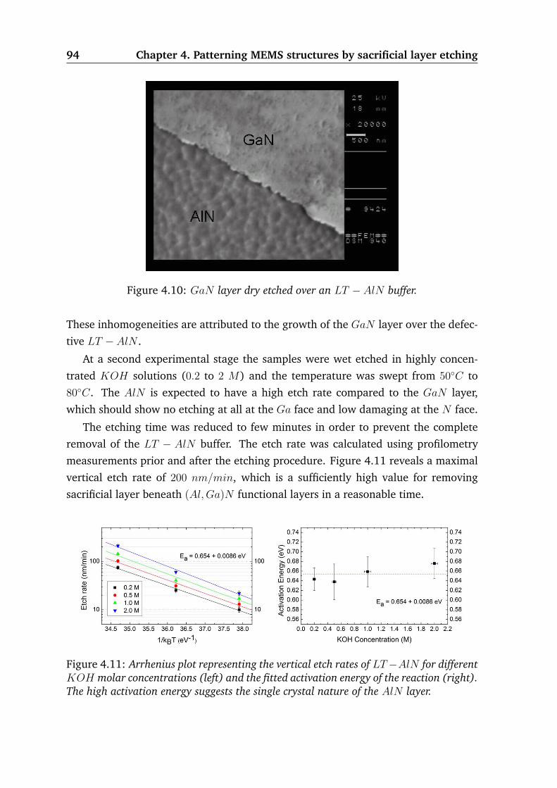
94 Chapter 4. Patterning MEMS structures by sacrificial layer etching
Figure 4.10: GaN layer dry etched over an LT − AlN buffer.
These inhomogeneities are attributed to the growth of the GaN layer over the defec-
tive LT − AlN .
At a second experimental stage the samples were wet etched in highly concen-
trated KOH solutions (0.2 to 2 M) and the temperature was swept from 50C to
80C. The AlN is expected to have a high etch rate compared to the GaN layer,
which should show no etching at all at the Ga face and low damaging at the N face.
The etching time was reduced to few minutes in order to prevent the complete
removal of the LT − AlN buffer. The etch rate was calculated using profilometry
measurements prior and after the etching procedure. Figure 4.11 reveals a maximal
vertical etch rate of 200 nm/min, which is a sufficiently high value for removing
sacrificial layer beneath (Al,Ga)N functional layers in a reasonable time.
Figure 4.11: Arrhenius plot representing the vertical etch rates of LT−AlN for differentKOH molar concentrations (left) and the fitted activation energy of the reaction (right).The high activation energy suggests the single crystal nature of the AlN layer.

4.2. Patterning of (Al, Ga)N/LT-AlN structures 95
Figure 4.12: SEM micrographs of the surface of GaN/LT − AlN samples after longKOH etches. The decomposition of the GaN layer into hexagonal pyramids is clearlynoticeable.
The repetition of the etching experiments showed a very good reproducibility of
the etch rate and a clear linearity of etched depth versus etching time. The linearity
of the etched depth is interpreted as that the thin AlN layers within the buffer grown
at optimal temperature have little influence on the etch rate. Nevertheless, the pres-
ence of these layers behaved as excellent etch stopping layers for the dry etching, as
discussed above.
The measured etch rates are represented on an Arrhenius plot for calculating the
activation energy of the process. As showed on figure 4.11, the activation energy
is constant for the different KOH concentrations. The achieved mean activation
energy was Ea = 0.654 eV , close to 0.67 eV , the characteristic value of the wet
etching of high quality AlN layers [122–124]. The small deviation is attributed to
the growth of the AlN layer at a suboptimal temperature. Nevertheless, the value of
Ea is indicative of a rate limited reaction, typical for single crystal materials.
4.2.2 Micromechanised GaN/LT-AlN structures
After the calibration of the vertical etch rate long wet etches were performed for
fabricating micromechanised GaN structures. The etched samples were studied by
SEM and it was observed that the GaN layer decomposed during the etching. As
shown in figure 4.12, the GaN after the etching does not form a continuous layer
but clusters of small hexagonal pyramidal structures. These pyramids are formed
along crystallographic planes of the wurtzite structure. The mean diameter of these
structures is slightly larger than 500 nm.
This behavior is typical for large defect density material. These materials suffer

96 Chapter 4. Patterning MEMS structures by sacrificial layer etching
Figure 4.13: GaN/LT − AlN sample etched with nickel mask. It is observed a slightunderetching under the metal mask.
from low coalescence during growth, originating a large amount of grain boundaries,
where the etchant may penetrate. Nevertheless, due to the special growth conditions
of the sample a phase reversion could have happened, attaining an N -phase upper
face [133–136], and not the expected Ga phase. In order to verify this hypothesis a
sample with a nickel mask was etched under the same conditions. Figure 4.13 shows
that the GaN protected under the metal mask was also etched, which is not typical of
high quality layers. Consequently, the decomposition of the layer may be attributed
to a large defect density induced during growth.
Structural characterization of the GaN/LT − AlN heterostructures
In order to asses that the heterostructures used for the etching investigation were
grown with a large defect density, a complementary HRXRD and AFM study was
performed. A reflexion measurement of the (0002) direction using a θ/2θ sweep
revealed that at the GaN angle there was no peak present. Actually, as shown in
figure 4.14, a plateau of width larger than 1 was detected. Therefore, it may be con-
cluded that the GaN layer atop the LT −AlN is polycrystalline showing a significant
misorientation. Nevertheless, at the AlN angle a strong peak is observed, indicating
its single crystal nature, as determined by the etching experiments. The width of the
peak is due to the variation of the temperature during the AlN growth.
For estimating the deformation state of the GaN layer, the (0004) reflection was
observed for separating the peaks, and a 0.5 mm slit was used. The slit filtered out

4.2. Patterning of (Al, Ga)N/LT-AlN structures 97
Figure 4.14: HRXRD reflection of the GaN/LT − AlN wafer used in this study. Thewidth of the AlN peak is attributed to the various temperatures used during the layergrowth. The plateau observed for the (0002) reflection (left) is due to a polycrystallineGaN layer. The measurement with a slit of the (0004) reflection (right) indicates thatthe layer is fully relaxed due to the large defect density.
the plateau allowing the main component to be observed. The GaN peak appears to
be almost completely relaxed, the calculated residual stress is 88 MPa which is much
smaller than the typical stress values for GaN layers grown on AlN [112,137,138].
The large defect density induced during growth is believed to be responsible for the
strain relaxation of the GaN layer.
Figure 4.15: AFM measurement of the GaN/LT −AlN sample. A GaN polycrystallinesurface is clearly observed.

98 Chapter 4. Patterning MEMS structures by sacrificial layer etching
Lastly, AFM measurements were performed for investigating the polycrystalline
nature of the GaN layer, by using the tapping mode in order to minimize the lateral
forces. As shown in figure 4.15 the surface shows a granular morphology with a grain
size from 1000 nm to 2500 nm. However, these large grains show a finer structure
composed of coalesced grains of 100 nm to 500 nm. The size of these fine structures
is consistent with the pyramids observed at the KOH etching experiments.
4.3 Patterning of (Al, Ga, In)N/Si(111) structures
In the above discussions it has been stated many times that the processing of III-N
materials is very challenging due to their chemical stability. However, it is possible to
produce III-N materials on processing friendly materials such as Si(111). The quality
of the nitrides semiconductors grown on silicon has improved from early days and it
is nowadays comparable to wafers produced on SiC or sapphire [28,139–141]. The
chemical nature of these materials is very different and it is possible to find a nice se-
lective etch in order to use the silicon as both, growth substrate and sacrificial layer.
Consequently, silicon sacrificial layers were considered as the primary approach for
the MEMS fabrication, and the above experiments were performed as alternative ap-
proaches. Silicon is largely used in MEMS industry and, therefore, there are plenty
of etching techniques available for the micromachining. In this dissertation two tech-
niques have been used:
• Wet etching in HF −HNO3 − CH3COOH (HNA) solutions
• Dry etching in SF6 plasmas
Other alternatives may be found in the literature. KOH and trans-3-Methyl-
2-hexenoic acid (TMHA) are two commonly used wet etchants but they produce
etches with rates depending on the crystallographic orientation. This effect is not de-
sirable since for the sacrificial etching the isotropy is the main figure of merit. For this
reason HNA-based etches have been investigated. The isotropy requirement may be
relaxed if the etch is made from the back side of the wafer. However, backalignment
was not available for this thesis and, thus, only etches performed on the functional
side of the wafer have been considered. On the other hand, there are several gas
combinations for the dry etching of silicon. The highest isotropy is obtained with
XeF2 [142, 143], but special equipment is required in order to perform the etching
with this gas. Unfortunately, this equipment was not available in our facilities, and
an alternative method had to be used. It is known that under certain conditions

4.3. Patterning of (Al, Ga, In)N/Si(111) structures 99
SF6 plasmas produce an etch with a very high isotropy. Therefore, in the follow-
ing paragraphs the optimization of the sacrificial etching of silicon substrates with
HNA and SF6 plasmas will be described and their application to the fabrication of
demonstrators will be presented.
4.3.1 Wet isotropic etching of Si(111)
As explained above, HNA was used for the wet chemical etching of silicon sub-
strates. The HNA is a well known etchant in silicon VLSI technology [142] and is
composed from a combination of three acids:
• Nitric acid.
• Acetic acid.
• Hydrofluoric acid.
The reaction which leads to the etching of silicon is very complex but may be
summarized as follows [142]:
• The HNO3 is dissociated in the acetic acid to form HNO−3 +H+.
• The HNO3 combines with HNO2 present in the dissolution to form water and
NO2.
• Sites on the silicon surface act as a cathode and provide electrons to form NO−2 .
• The NO−2 reacts with H+ to form HNO2 until equilibrium is reached and the
reaction is maintained.
• The holes produced at the cathode sites combine with silicon atoms to form
Si2+.
• The Si2+ reacts with OH− groups present at the dissolution to form SiO2. Due
to the hole diffusion law this oxide is isotropically generated on all the exposed
surface, originating a very isotropic etch.
• Finally, the SiO2 is dissolved in HF .
The process is very complex and needs a balance between the reactants in order
to maintain the described reaction and provide a controllable and reproducible etch.
Therefore, an optimization on Si(111) growth substrates has been performed as part

100 Chapter 4. Patterning MEMS structures by sacrificial layer etching
Figure 4.16: Studied HNA combinations and the obtained vertical and lateral etch rateswithout agitation.
of this thesis work. Various combinations of acids were used under different agitation
conditions.
It was soon observed that agitation promoted the isotropy, whereas without ag-
itation the lateral etch component was very small. The etch rates obtained by this
method have been very high and have been depicted in figure 4.16 for the stud-
ied etching solutions. The lateral etch rate sweeps a range between 2 µm/min to
16 µm/min. These values are appropriate for MEMS device processing and allow the
selection of an adequate etching for the device size and geometry.
The surface morphology was analyzed by SEM after the etch. Silicon plays a
passive role in MEMS devices but a uniform surface is preferred for several reasons.
First, silicon may be used as back contact and therefore the absence of spikes in
the etched regions will avoid the formation of field concentrations which may affect
the performance of the device. Secondly, a smooth clamping region is desirable in
order to provide uniform boundary conditions to the moving parts of the device.
Figure 4.17 shows that the etched surface morphology depends mainly on the ratio
between the concentrations of HF and HNO3. For the studied conditions, the ratio
Figure 4.17: Surface morphology of silicon (111) wafers after HNA sacrificial wet etch-ing with HF : HNO3 ratio 1 : 3 (left), 2 : 3 (center) and 3 : 3 (right).

4.3. Patterning of (Al, Ga, In)N/Si(111) structures 101
Figure 4.18: Gold microbridges fabricated on Si (111) by HNA sacrificial wet etching.
providing the smoother surfaces was HF : HNO3 (2 : 3).
In order to asses the possibility of using this process for the fabrication of MEMS
devices, metal structures where mechanized. These experiments were performed in
order to optimize the etching procedure and the drying technique. A thick gold layer
(1 µm) was deposited on silicon (111) wafers, previously cleaned with a buffered ox-
ide etch solution (HF : NH4F ). The results were good and showed that the vertical
component of the etching avoided the formation of capillaries which could make the
structures collapse. However, in order to fully avoid sticking the samples were rinsed
in deionized water and then in isopropanol. After the rinse and before the evapora-
tion of the solvent the samples were placed on a hot plate at a temperature above
100C. By this procedure, sticking was completely avoided and structures such as the
one shown in figure 4.18 were produced.
4.3.2 Dry isotropic etching of Si(111)
As described in the previous paragraph a wet isotropic etching technique of silicon
substrates was optimized for the etching of nitride MEMS. However, this method
presents several disadvantages among which the most important is that it is difficult
to have a precise control of the underetch length. For this reason, when using wet
etching, it is possible to produce too much under etching at the clamping regions
and therefore reduce the device performance. Other disadvantage common to wet
etching techniques is that such methods usually produce an irregular etch and that
there may be contaminants left on the surface after the processing. Thus, in order
to avoid these undesirable side effects, another etching method was required and
pursued in this thesis.

102 Chapter 4. Patterning MEMS structures by sacrificial layer etching
Dry etching is usually preferred because it produces cleaner, more regular and
controllable etches compared to wet etching techniques. The main problem that
the dry etching presents is that it produces normally rather anisotropic etch profiles.
Therefore, it is important to find a gas and plasma conditions which maximize the
lateral etching component of the silicon etch. Selectivity is also fundamental at this
step. A mild plasma which would only etch the silicon and would not neither etch the
nitrides nor induce defects due to bombardment has to be found. For this purpose
the RIE reactor described at chapter 2 has been used and SF6 has been chosen as
etching gas.
Fluorine and chlorine plasmas etch silicon [143, 144] whereas if fluorine plasma
is used to etch (Al,Ga)N an (Al,Ga)F3 passivation will be created on the surface
and the etch will be stopped. In practice a slow etch rate is observed because some
molecules of this passivation layers are removed by physical sputtering leaving the
nitrogen plane exposed to the plasma and, as discussed at 3.1, the nitrogen planes
are efficiently removed in fluorine plasmas. For this reason, it is very important to
use very mild plasma conditions. The low directionality pursued leads to mild plasma
conditions as well, if a high DC voltage plasma is used the radicals in the plasma will
be accelerated and will result in an anisotropic etch.
The conditions which has been used for the optimization study are:
• Gas: SF6 (due to the high pressure and flux no other gas has been necessary
for stabilizing the plasma)
• Flux: 10 − 15 sccm
• Pressure: 40 − 60 mtorr
• DC voltage: 40 − 50 V
For all the studied conditions no etch step has been observed on a reference GaN
wafer which was introduced together with the silicon samples in the etch reactor.
The exposed silicon areas were efficiently etched, and a significant amount of lateral
etching was observed for all conditions. The etching results for all the studied con-
ditions are shown in figure 4.19, where it is possible to observe that, although the
vertical etch rate is higher, there exists a significant amount of lateral under etching.
It is observable that the higher the pressure, the higher is the proportion of the
lateral etch rate compared to the vertical etch rate, going from 35% for 40mtorr up to
40% for 60 mtorr. What is also remarkable is that if the plasma DC bias is increased
from 40 V to 50 V , the proportion of the lateral etching compared to the vertical etch

4.3. Patterning of (Al, Ga, In)N/Si(111) structures 103
Figure 4.19: Vertical and lateral etch rates for dry silicon sacrificial etching in SF6
plasma.
rate falls below 25%. However, experiments performed at even lower DC voltages led
to non stable plasmas and therefore slow and inhomogeneous etches. Thus, for the
equipment used in this thesis work an optimum DC voltage has been identified to be
40 V . As mentioned before, when increasing the chamber pressure, the proportion
of lateral etching to vertical etching is favored. However, the absolute highest lateral
etch rate is obtained for 50 mtorr because for higher pressures reactions and colli-
sions within the plasma cause the etch rates to fall. Further increase in the pressure
was not possible with the available equipment and a detailed study of the interac-
tions in the plasma could not be carried out, and in any case such study falls out of
the scope of the present thesis.
Finally, the influence of the flux was observed on the absolute etch rates. When
increasing the flux of the gas the residence time of the radicals is also increased
and therefore, as with increased pressure, the etch rates are lower due to enhanced
interactions within the plasma. However, it has been observed that both the vertical
and lateral etch rates are reduced in the same proportion, remaining the rate ratio
unchanged when the total flux is varied.
As a result of this research, the optimal etching conditions for sacrificial under-
etching of Si(111) substrates have been identified. These conditions will be used for
the rest of the dissertation with minor adjustments in order to tune the etch rate:
• Gas: SF6
• Flux: 10 sccm
• Pressure: 50 mtorr

104 Chapter 4. Patterning MEMS structures by sacrificial layer etching
• DC voltage: 40 V
• Achieved lateral etch rate: 80 − 83 nm/min (depending on the quality of the
substrate)
4.3.3 Micromechanised (Al, Ga, In)N/Si(111) structures
After the etching technique optimization the wet etching and the dry etching
were applied to the fabrication of free-standing structures. For this purpose nitride
structures on silicon where etched with the above conditions in order to check for
selectivity and the possibility of etching wide structures in order to liberate cantilever
and bridge structures. In the case of nanocrystalline diamond (NCD) on silicon, was
also etched using the above described wet etching procedure but the dry etching was
performed in the Fraunhofer Institut für Angewandte Festkörperphysik in Freiburg.
Therefore a different reactor was used for the dry etching, namely, an ICP reactor
with a similar SF6 plasma to the one optimized in this thesis was used.
Etching of nitride structures
In order to asses the compatibility of the sacrificial etching procedures with the ni-
tride technology, several experiments were carried out on different materials. GaN ,
AlGaN and InN structures on Si(111) were patterned using the dry etching proce-
dure described at chapter 3 and subjected to different sacrificial etches. As nitride
structures on silicon were used for the optimization of the wet and dry etches the se-
lectivity of the etching procedure was already established. Figure 4.20 shows a SEM
micrograph of underetched nitride structures in order to demonstrate that an excel-
lent selectivity is achieved, as no etch was measured on the nitride semiconductor
surface. In any case it was observed etching of neither GaN , AlGaN nor InN in any
Figure 4.20: Cross section of underetched InN (left), GaN (center) and AlGaN (right)sample showing no etching at all.

4.3. Patterning of (Al, Ga, In)N/Si(111) structures 105
Figure 4.21: Comparison of nitride structure underetching in SF6 (right) plasma andHNA(left) solution.
of the dry or wet etching procedures. Therefore, the compatibility of the fabrication
process is assured.
With both procedures it has been possible to successfully underetch wide (up to
8 µm) nitride structures as shown in figure 4.21. It is observed that while both pro-
cedures allow the fabrication of free-standing structures, the dry etching provides
much better results in terms of surface contamination after etching, smoothness of
the etched area and specially in terms of uniformity of the clamping area. For a cor-
rect performance of the device, it is of utmost importance to control the uniformity of
the boundary conditions and therefore to ensure that no irregularities in the clamp-
ing region are induced during the sacrificial etching procedure. For these reasons
the dry etching will be generally preferred. Other reason for the preference of the
dry etching is that the SF6 plasma will only etch metals due to ion bombardment.
Nevertheless, the mild plasma conditions used in this work ensure the compatibility
of the procedure with most metals. On the contrary, HNA etching is not compatible
with aluminum due to the HF content which etches very efficiently thin aluminum
layers.
Etching of nanocrystalline diamond structures
As with the nitride structures, the same assessment procedure was employed with
nanocrystalline diamond layers deposited on silicon (001) substrates. The deposition
conditions were varied in order to produce high quality NCD layers with grain sizes
below 70 nm, although without adding as much methane as to degrade the mechan-
ical properties. The NCD wafers were dry etched, in order to transfer a pattern for
the sacrificial etch calibration, using the plasma procedure described in section 3.5.
It has been observed that both dry and wet etching procedures produce the under-
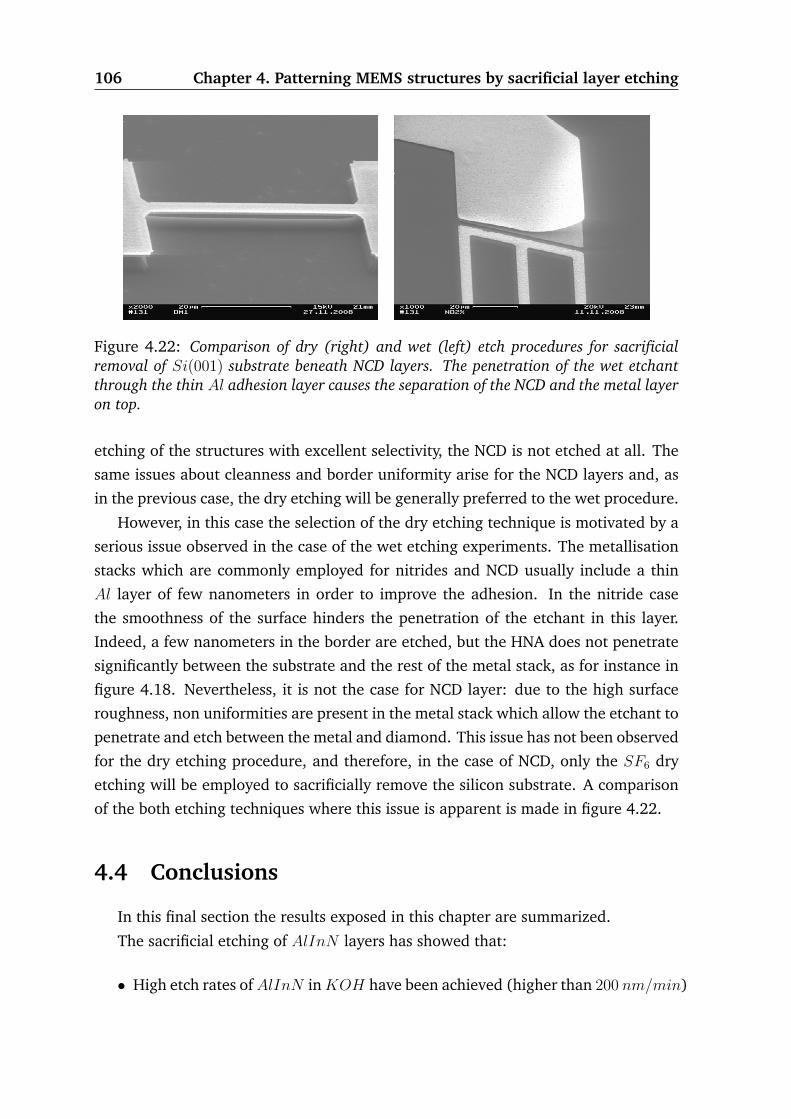
106 Chapter 4. Patterning MEMS structures by sacrificial layer etching
Figure 4.22: Comparison of dry (right) and wet (left) etch procedures for sacrificialremoval of Si(001) substrate beneath NCD layers. The penetration of the wet etchantthrough the thin Al adhesion layer causes the separation of the NCD and the metal layeron top.
etching of the structures with excellent selectivity, the NCD is not etched at all. The
same issues about cleanness and border uniformity arise for the NCD layers and, as
in the previous case, the dry etching will be generally preferred to the wet procedure.
However, in this case the selection of the dry etching technique is motivated by a
serious issue observed in the case of the wet etching experiments. The metallisation
stacks which are commonly employed for nitrides and NCD usually include a thin
Al layer of few nanometers in order to improve the adhesion. In the nitride case
the smoothness of the surface hinders the penetration of the etchant in this layer.
Indeed, a few nanometers in the border are etched, but the HNA does not penetrate
significantly between the substrate and the rest of the metal stack, as for instance in
figure 4.18. Nevertheless, it is not the case for NCD layer: due to the high surface
roughness, non uniformities are present in the metal stack which allow the etchant to
penetrate and etch between the metal and diamond. This issue has not been observed
for the dry etching procedure, and therefore, in the case of NCD, only the SF6 dry
etching will be employed to sacrificially remove the silicon substrate. A comparison
of the both etching techniques where this issue is apparent is made in figure 4.22.
4.4 Conclusions
In this final section the results exposed in this chapter are summarized.
The sacrificial etching of AlInN layers has showed that:
• High etch rates ofAlInN inKOH have been achieved (higher than 200 nm/min)

4.4. Conclusions 107
while keeping a high selectivity with GaN .
• The high activation energy of the etching process (0.64 eV < Ea < 0.68 eV )
is an evidence of the high crystal quality of the used samples.
• The etch rate has been found to depend on the KOH concentration, increasing
with the etchant molarity. Nevertheless, the etch rate saturates at a certain
etchant concentration, which depends on the crystal quality of the material.
• An increased etch rate has been observed at the defect sites.
Free-standingGaN structures have been obtained with this sacrificial layer. However,
the high crystal quality of the samples has hindered the fabrication of large structures.
During the experiments it has been observed that a certain accumulation of defects
on the sacrificial layer is beneficial for the etching.
The observations made for the AlInN etching led to proposing an alternative sac-
rificial material, low temperature AlN . Nevertheless, the attempts to etch a sacrificial
layer of GaN on LT −AlN were not successful due to the extreme difficulty of over-
growing a functional material with the sufficient quality over the material grown at
low temperature. The LT −AlN layers used for this dissertation apparently formed a
single crystal, as determined from XRD and the high activation energy of the etching
reaction, but the GaN layers grown on top were polycrystalline. In order to use this
approach, a previous optimization work of the growth technique has to be performed,
which is far beyond the scope of the present thesis.
An alternative to the compound sacrificial layers is the use of material grown
over silicon. From the vast amount of silicon etching techniques, two of them are
proposed because they have showed both high etching rates, vertical and lateral, and
large selectivity with the functional materials proposed in this thesis. The etching
processes that have been used successfully to produce III-N and NCD free-standing
structures are:
• Wet etching in HNA solution, with the aid of agitation.
• Dry reactive ion etching with SF6 plasmas using high flux and high chamber
pressure.
Both techniques have been used to fabricate MEMS structures, but the dry etching
is preferred because it is cleaner and more controllable. Moreover, for the NCD pro-
cessing the wet etching technique is not recommended because the high roughness
of the NCD surface promotes the etching of the typical metalization stacks, rendering

108 Chapter 4. Patterning MEMS structures by sacrificial layer etching
the etching incompatible with the metalization of the surface. Nevertheless, if large
structures are to be underetched, the HNA may be appropriate due to the extremely
high etching rates that can be attained.

Chapter 5
AlN deposition by pulsed DC reactivesputtering
Sputtered polycristalline AlN layers may be used as a piezoelectric driving layer
for III-N and NCD MEMS. It has been demonstrated that polycristalline AlN can be
used for surface acoustic wave devices on NCD with excellent results [145, 146].
However, for MEMS, extremely thin layers of AlN are required for an efficient driv-
ing, as will be discussed in chapter 9. Thus, the first stage of the growth is a consid-
erable proportion of the AlN layer. For SAW applications, the thin adaptation layer,
present at AlN deposited by sputtering under certain conditions [147–150], has not
a big impact on device response. However, this is not true for MEMS.
In this thesis the boundary between amorphous and texturized deposition of AlN
has been explored. Deposition parameters have been varied in order to identify
the region where thin (d ≤ 120 nm) AlN films turn from amorphous to texturized
growth region. The presence of a preferential orientations of such films is of utmost
importance for the fabrication of efficient piezoelectric driving layers for III-N and
NCD MEMS structures. The optimization ofAlN for SAW devices has been performed
in the PhD thesis by Dr. J. G. Rodríguez [87,151].
This work was performed in collaboration with J. Zugasti [152] at the ISOM
facilities.
5.1 Experimental procedure
Two power to pressure mappings have been performed for the sputtering deposi-
tion of AlN . Pressure, voltage and target to substrate distance are the most relevant
parameters used to control the transition between growth regimes [153–155]. Other
109

110 Chapter 5. AlN deposition by pulsed DC reactive sputtering
influential parameters such as reactive to inert gas ratio and temperature have been
fixed for this research. The temperature has been fixed to room temperature and the
gas ratio was fixed to 50% following previous work [86] for AlN film deposition.
The process parameters were selected to explore the boundary between texturized
and amorphous layer growth. The selected values are:
• Pulsed DC power, P : 100, 175 and 250 W
• Chamber pressure, p: 1, 2, and 5 Pa
• Target to substrate separation, dts: 50 and 70 mm
For establishing the total gas flux a previous calibration was performed. Power
sweeps from 50 to 350 W were performed with total fluxes from 10 to 100 sccm. It
was obtained that at 30 sccm the plasma was stable for discharge powers higher than
75 W . With the pumping system fully opened the chamber pressure was 7 mtorr
which roughly corresponds to the lowest pressure selected for the pressure. Hence,
the total flux was fixed to 30 sccm and the pressure in the chamber was controlled
closing the throttle valve of the pumping system.
For each studied point two layers were deposited with nominal thicknesses of
60 and 120 nm. For controlling the deposition rate, preliminary depositions were
performed for both dts. The obtained deposition rates (v) were used to estimate the
deposition rates for the studied parameter set using
v′ ≈ v
√δP
δp(5.1)
Good agreement between the predicted thickness and the finally measured value
were observed for all the deposition conditions. The thickness of the deposited ma-
terial was verified by profilometry on test samples that were deposited at the same
time as the study samples by means of a shadow mask (see below).
Figure 5.1: Sample structures used in the AlN deposition research.

5.2. Deposition rate 111
The AlN deposition was performed on silicon substrates. Two samples were de-
posited simultaneously at every study point, a bare Si(001) and a metalized sample.
This samples were used to measure structural and electrical characteristics of the
deposited material, using metal-insulator-semiconductor (MIS) and metal-insulator-
metal (MIM) structures. The metalization over which the deposit was performed is
Au (100 nm) with a thin Ti adhesion layer (20 nm).
The obtained results may vary for different substrates, but qualitative conclusions
about the trends that lead to the formation of the thin adaptation layer can be ex-
tracted. It is worth to note that both substrates provide a interface for the AlN
deposition with very low roughness. Therefore, in order to extrapolate the observa-
tions to NCD it would be necessary to deposit on the back surface of the diamond or
to polish the upper surface of theNCD layer.
5.2 Deposition rate
The deposition rate has been measured on a test sample placed in all the deposi-
tion processes. This sample was partially covered with a shadow mask and the step
was measured by profilometry.
It has been seen that the deposition rate follows well the relation given by 5.1.
A large difference is observed when varying dts: for the 50 mm configuration the
measured rates are more than double than for the 70 mm configuration. Very high
etch rates have been achieved with maximum values of 15.5 nm/min and 6 nm/min
for the 50 mm and 70 mm configurations, respectively. The complete set of measured
values has been represented at the figure 5.2.
Figure 5.2: AlN deposition rate.

112 Chapter 5. AlN deposition by pulsed DC reactive sputtering
Such large deposition rates may have a big impact on the structure and orienta-
tion of the film [156]. This impact will be discussed when interpreting the results of
the structural characterization.
5.3 Structural characterization
The structural characterization of the deposited material was analyzed in order to
asses the degree crystallinity. This information is useful for determining the growth
regime boundaries and for helping in the interpretation of the electrical measure-
ments. The material organization was explored by HRXRD, the composition was
verified by FTIR spectroscopy and the morphology was characterized by AFM. In
what follows the findings by these three techniques are discussed.
In this section, the results of the depositions of AlN over silicon will be discussed.
The depositions made over the Au metalization could not be measured by FTIR spec-
troscopy but the XRD and AFM analysis showed no substantial difference with the
results obtained for samples deposited directly over silicon. Finally, a subset of films
deposited over Au were analyzed using the piezoresponse setup described at 2.6.3.
The results were completely coherent with the predictions made from the results
obtained for the AlN/Si(001) samples.
5.3.1 X-Ray diffraction
The preferred orientation of the AlN films deposited by reactive sputtering is the
(00.2) orientation. Nevertheless, under certain growth conditions the (10.0) and
(10.1) are also present [153, 154, 156]. The formation of the different planes is
related with the energy with which the adatoms reach the surface were they react to
form the film [157].
Target substrate distance [154] and pressure-power relation [153] determine the
AlN deposition mode and the preferred orientation of the film, if the growth condi-
tions lead to a texturized layer. In the wurtzite crystal two types of Al −N bondings
are formed, B1 and B2. The formation energy of the B2 bonds is higher then for
B1 bonds. The (10.0) plane is formed by B1 bonds whereas the (00.2) and (10.1)
are formed by B2 bonds. Thus, for favoring the (00.2) and (10.1) directions, higher
energy adatoms are required.
Other factors that influence the orientation of the AlN film are:
• The deposition rate. Low rates favor closed packed crystallization as the adatoms
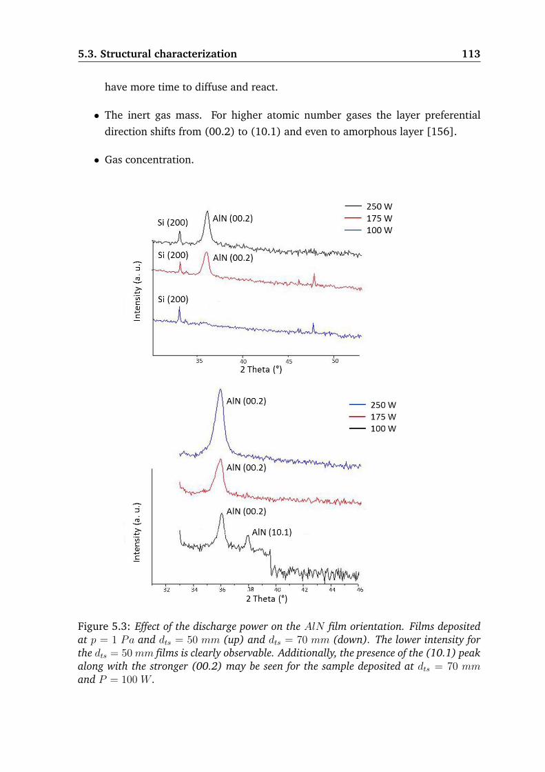
5.3. Structural characterization 113
have more time to diffuse and react.
• The inert gas mass. For higher atomic number gases the layer preferential
direction shifts from (00.2) to (10.1) and even to amorphous layer [156].
• Gas concentration.
Figure 5.3: Effect of the discharge power on the AlN film orientation. Films depositedat p = 1 Pa and dts = 50 mm (up) and dts = 70 mm (down). The lower intensity forthe dts = 50 mm films is clearly observable. Additionally, the presence of the (10.1) peakalong with the stronger (00.2) may be seen for the sample deposited at dts = 70 mmand P = 100 W .

114 Chapter 5. AlN deposition by pulsed DC reactive sputtering
A profound discussion on the deposition mechanics is provided at [158] and ref-
erence therein.
The XRD measurements of the polycristalline AlN layers were performed in the
Instituto de Ciencia de Materiales (Madrid) by Dr. Ana Ruiz. A D8 Bruker diffrac-
tometer, without monochromator, was used. The general tendencies observed at the
XRD analysis is that (00.2) peak appears for high energy adatoms. The (00.2) peak is
detected for depositions made at p = 1 Pa. For higher pressures only at dts = 70 mm
and P ≥ 175 W , a small (00.2) peak has been detected. Analogously, as the power
is increased the formation of (00.2) oriented films is favored. The (10.1) orientation
peak was measured for samples deposited either with low pressure (p = 1 Pa) and
low power (P = 100 W ), or with intermediate pressure (p = 2 Pa and p = 5 Pa only
for dts = 70 mm) and high power (P ≥ 175 W ). In summary, the (00.2) orientation
is the preferred orientation but is formed only for high energy adatoms; if the energy
of the adatoms is reduced the (10.1) orientation peak appears, and if the energy is
further reduced amorphous layers are deposited.
The dts influence requires a separate analysis, contrary to what was expected
[154], the layers deposited with greater dts showed more intense XRD peaks. This
could be explained by the elevated deposition rate of the material deposited at
dts = 50 mm; if the rate is high the adatoms do not have time to diffuse and an
amorphous layer is formed [156]. The competing deposition mechanisms tend to
form an oriented layer after the first stages of growth of this amorphous film [147],
thus explaining that the (00.2) peak appears but much weaker than for films de-
posited under same pressure-power conditions but with larger dts. This hypothesis is
reinforced by the observation of the layer thickness influence. The 60 nm thick sam-
ple deposited at dts hardly showed an (00.2) peak for the more energetic conditions
(p = 1 Pa and P = 250 W ,) whereas a small but appreciable peak was measured for
the samples deposited at dts = 70 mm.
5.3.2 FTIR spectroscopy
FTIR spectroscopy for AlN sputtered layers has been long established [159,160].
It provides a qualitative measurement of the crystal quality, related with the width of
the absorption peaks, and the residual stress in the layer, related with the position of
the peaks. In this section both figures of merit for the deposited material with 120 nm
thickness are discussed. For additional determination of the deposition dynamics
some of the 60 nm thick films were studied.
The FTIR has been measured using the transmission setup and a Si(001) back-

5.3. Structural characterization 115
Figure 5.4: FTIR spectrum of a sputtered AlN layer.
ground measurement was performed before each AlN measurement in order to sub-
tract the Si contribution. The transverse optical modes E1(TO), at 672 cm−1, and
A1(TO), at 612 cm−1 have been measured. The presence of each peak is related with
the B2 and B1 bondings respectively [161]. It has to be noted that the A1(TO) mode
has not been resolved for all the deposition conditions as it is much weaker than the
E1(TO) peak for all spectra. In our experiments, the measurements of the A1(TO)
peak were very difficult because of the low level of the peak and the overlapping
with the E1(TO) peak. Hence the FWHM measurement of the A1(TO) peak are very
unreliable.
Analyzing the FWHM of the E1(TO) absorption peak shows a decrease as the
energy of the adatoms is increased. The higher energy of the adatoms allows the for-
mation of better crystalline structures and thus to the width reduction of the E1(TO)
peak. As pressure is reduced or discharge power is increased, a fall in the FWHM
of the FTIR peak is observed. From figure 5.5 it is observed that a big reduction is
obtained when increasing P from 100 W to 175 W , being this effect much higher for
the larger dts configuration. Varying dts has also a large impact in the FWHM of the
E1(TO) FTIR peak. It is clear that for low texturized films, the FWHM of the peak for
Figure 5.5: Width (left) and displacement (right) of the E1(TO) peak on the FTIRspectra.

116 Chapter 5. AlN deposition by pulsed DC reactive sputtering
Figure 5.6: Layer thickness influence on the FTIR spectrum of a sputtered AlN film.
dts = 70 mm is much larger than for dts = 50 mm.
Analyzing the position of the E1(TO) peak the residual stress in the AlN film
may be determined [162]. The measurements reveal that the samples deposited
at the dts = 50 mm configuration have a much lower residual stress than for the
dts = 70 mm configuration. The power and pressure have an analogous effect than
for the FWHM, as the energy of the adatoms is increased the residual stress falls.
Actually at the more energetic configuration (dts = 50 mm, P = 250 W , p = 1 Pa),
the residual stress turns to compression in contrast to the other conditions were
tensile stress was measured. Nevertheless, it is observed a tendency to turn toward
compressive stress if pressure in the chamber is increased, as seen for the p = 5 Pa
points.
The data points with higher pressures for dts = 70 mm and P = 100 W have
been left out of the discussion due to the high displacement that has been measured.
This defective data points correspond to spectra where the width of the peak was
extremely large (> 400 cm−1), so the exact peak position determination is prone to
errors. It is unclear if such a large width and displacement is due to stress or contam-
ination in the layer. These samples have shown clearly amorphous AlN films so the
contamination hypothesis may not be discarded, as it is known that contamination
drastically hinders the formation of texturized layers [153].
By analyzing the 60 nm thick sample, the same tendencies are observed but much
weakened. The residual stress for all the studied samples was much lower and the

5.3. Structural characterization 117
peaks were wider. This effect suggests the existence of an adaptation layer. Indeed,
for the samples deposited at dts = 50 mm the drop in the E1(T0) peak width as
the films get thicker is a sign that a thick adaptation layer exits. The low stress of
the films deposited at dts = 50 mm is explained by the fact that adaptation layers
form plenty of defects that help the stress relaxation. When the oriented deposition
starts to take place, the grains adapt to the amorphous layer and less stress is build
up [147]. For the films deposited at dts = 70mm the deposition rate is lower and thus
the adaptation layer is thinner, as the adatoms have time to diffuse and react to form
oriented grains. The thinner adaptation layer hinders a complete stress relaxation so
that bigger residual stress is attained.
The measured stress values for the deposited material are high, ranging from
0.9 GPa compressive to 3.98 GPa tensile for dts = 50 mm, and 1.1 GPa compressive
to 3.97 GPa tensile for dts = 70 mm. These values are high for MEMS fabrication and
will induce a deformation or stiffening of the free-standing structures. For the high
energetic configuration (dts = 50 mm, P = 250 W , p = 1 Pa), the measured stress is
lower than for the other configurations. It also provides the better texturized films,
thus being the ideal conditions for AlN deposition for MEMS, from the microme-
chanical point of view. From this configuration, an optimization has to be made for
further reducing the residual stress while improving the orientation for enhancing
the piezoelectric response.
5.3.3 Piezoresponse
Piezoresponse was measured for the MIM structures with 120 nm AlN thickness
for the samples deposited at the following conditions:
• dts = 50 mm, p = 2 Pa, P = 175 W
• dts = 50 mm, p = 2 Pa, P = 250 W
• dts = 50 mm, p = 1 Pa, P = 175 W
• dts = 50 mm, p = 1 Pa, P = 250 W
• dts = 70 mm, p = 1 Pa, P = 175 W
• dts = 70 mm, p = 1 Pa, P = 250 W
No response was observed for the samples deposited at p = 2 Pa, while a small
response was detected for p = 1 Pa. The sample deposited at higher power had a

118 Chapter 5. AlN deposition by pulsed DC reactive sputtering
more defined response than the samples deposited at P = 175 W , which provide
very low signal level. No clear influence of dts has been established due to the low
signal levels and instrumental artifacts. Indeed, problems with the instrumentation,
described at 2.6.3, hindered the quantification of the piezoelectric response. The
signal was very noisy and unstable making it impossible to obtain a reliable set of
values for comparing with the reference sample. Although good, the signal was so
weak that the piezoelectric response is believed not to be optimal. Further improve-
ment of the orientation of such thin films has to be done for fabricating efficient AlN
driven MEMS structures. Nevertheless, it has been proven that samples deposited at
p = 1 Pa and P = 250 W show a measurable piezoresponse for both dts for films as
thin as 120 nm.
5.3.4 Surface morphology
The samples deposited at dts = 70 mm that showed higher ordering were exam-
ined under AFM. The gain size and roughness of the texturized surface was inves-
tigated. The surface morphologies of samples with strong (00.2) orientation show
regular granular surface with a low dispersion of the grain size. On the opposite, the
samples where the orientation was measured to be weak, the regular granular sur-
face is mixed with irregular grains. It must be stated that all the investigated samples
were perfectly coalesced and no pinhole or void has been seen for any of the studied
films.
The surface RMS roughness has been found to vary between 3 and 4.5 nm with
Figure 5.7: AFM surface measurement of a highly (left) and poorly (right) texturizedAlN layer.

5.4. Electrical characterization 119
no clear dependence on the deposition conditions. In contrast, the grains mea-
sured for texturized samples with high (00.2) XRD peak had sizes between 20 and
25 nm, regardless of the deposition conditions. Thus the deposition conditions seem
not to have a big impact on the surface morphology and (00.2) grains follow a
self organized growth once the deposition enters the columnar deposition region
[147,153,163].
5.4 Electrical characterization
The depositedAlN films were electrically characterized as explained in section 5.1.
Breakdown field, C-V and I-V characteristics were measured using MIS and MIM
structures. Nevertheless, the MIM structures with the thin amorphous films showed
elevated leakage currents due to the high defect density. Although the structural
characterization showed no difference in the film morphologies, the electrical char-
acterization of MIM structures was only possible for samples with good orientations.
In fact, MIM structures could only be used for piezoresponse characterization of thick
oriented layers.
As a result, the electrical characterization was performed only on the MIS struc-
tures. The Si(001) substrate was p doped with a resistivity of 5 − 10 Ωcm. The
backside of the Si wafer was contacted with a gold metalization using a Ti adhesion
layer. The AlN film was contacted with a Hg probe that formed the diode for the
measurements without the need of any processing, see figure 5.8.
Figure 5.8: MIS (left) and MIM (right) contact diagram used for the electrical charac-terization of the AlN deposited films.

120 Chapter 5. AlN deposition by pulsed DC reactive sputtering
5.4.1 Breakdown field measurements
The breakdown field measurement was done by increasing the supplied voltage
until a value that triggers a high current response. The threshold voltage is then
normalized to calculate the breakdown field. It must be stated that only for 120 nm
thick samples was a threshold measured.
The crystalline quality of the AlN film was observed to be determinant in the
threshold measurement. For low crystal quality samples a big increase in the leakage
current was found in the vicinity of the breakdown. This effect made the determina-
tion of the breakdown voltage difficult as the uncertainty of the calculated value was
very high. Conversely, for samples that showed a certain orientation, specially for
those deposited with dts = 50 mm, a well defined threshold voltage was determined.
The values measured for the films with good crystal quality oscillated from 2.3 to
2.8 MV/cm. No variation in the value was found with dts, being the only difference
that for 70 mm a current increase was observed before triggering the breakdown.
This value is lower than other breakdown field previously reported [164]. This is
believed to be due to the influence of the amorphous layer; the adaptation material
has poor dielectric properties and for such thin films it forms a significant proportion
of the total layer thickness.
5.4.2 Current-Capacitance characteristics
The samples were measured for determining the C-V characteristics. The voltage
was swept from accumulation (−13 V ) to inversion (10 V ) and back. The crossing
between regions induces a band flattening of the structure and the capacitance falls
to the flat band value (Cfb). The voltage that induces this state is called flat band
voltage (Vfb). The measurement of Vfb and the hysteresis provide information about
the charge density in the AlN film and the injected charge during the measurement.
A frequency sweep was performed for determining the optimal measurement
conditions. The capacitance values measured for accumulation and inversion are
different but tend to a similar value as the measurement frequency increases. Nev-
ertheless, the maximum capacitance drop at the flat band condition is obtained for
f = 100KHz and thus this frequency was selected for performing the measurements.
Charge density determination
The measurement and interpretation of C-V curves is a standard method for semi-
conductor characterization. Details on the measurement principles may be consulted

5.4. Electrical characterization 121
at [165]. In what follows a brief summary of the calculations used for the AlN
characterization is provided.
The flat band capacitance is given by
Cfb =ε0εAlNεSi
εAlNLD + εSidAlN(5.2)
where ε0, εAlN and εSi are the electrical permittivities of vacuum, AlN and Si,
respectively, dAlN the thickness of the AlN film and LD the Debye length. The Debye
length is calculated as
LD =
√εSiε0KBT
q2NSi
(5.3)
were KB is the Boltzmann constant, T the temperature in degrees Kelvin, q the
electron charge and NSi the dopant density of the silicon substrate. As all of these
are known quantities, LD is calculated to be approximately 40 µm.
Taking the calculated value for LD and the theoretical values for the electrical
permittivities, Cfb can be calculated. The variation due to the thickness of the AlN
layer is small (as dAlN LD) and will be masked by the uncertainties in other factors,
such as the exact dopant density of Si or the permittivities. Hence a constant average
value of Cfb is considered regardless the AlN thickness,
Cfb ≈ 2.59 · 10−6 F/m2 (5.4)
Taking into account the contact surface of the Hg probe results in
Cfb ≈ 4.4 pF (5.5)
The trapped charge in the dielectric layer is given by Vfb following
NF =
(φms − VfbqdAlN
)εAlNε0 (5.6)
where NF is the density of charge trapped in the dielectric layer and φms is the
work function of the metal-semiconductor contact.
It has to be stated that all the measurement provided a minimum capacitance very
close to the 4.4 pF value. The small variations could be attributed to uncertainties
in the values used in the calculation, but their magnitude has to be small as the
dispersion of the measured Cfb is also small (< 5%). Therefore, the value of the
electrical permittivity of the AlN layer can be assumed to be close to the theoretical

122 Chapter 5. AlN deposition by pulsed DC reactive sputtering
value of ε = 9.14.
Additionally, large capacitance hysteresis effect was observed when performing
the voltage sweep. The hysteresis turns counterclockwise so the effect is attributed
to hole carrier injection. When starting from the accumulation regions, holes are
injected in the dielectric, and when starting from inversion electrons are injected.
Therefore, the mean value of Vfb has been taken as an estimator of the charge trapped
in the dielectric and the hysteresis amplitude as an estimator of the charge injection.
Measurement results
A large dispersion in the measured values has been observed. The values of
trapped charge are high, between 8 · 1011cm−2 and 4 · 1012cm−2, and comparable
to other published results [164, 166]. The hysteresis effect produces densities of in-
jected charges of about an order of magnitude lower, from 1 ·1011cm−2 to 1 ·1012cm−2,
but following the trends of NF .
The only clear trend that has been identified is the fall of the trapped and injected
charge values as the layers get thicker. Indeed, the trapped charge value falls from
the range 2 − 4 · 1012cm−2 to 0.8 − 2 · 1012cm−2 as the AlN thickness evolves from
60 nm to 120 nm. This effect suggests that the majority of the carrier is trapped at the
interface [164, 166] and that some of it is removed during growth of thicker layers,
probably due to defect annealing by self-heating effect.
The rest of the data suggests a small decrease of the charge density value for
samples with greater texture, altough it is difficult to confirm due to the scarce data
points and the large dispersion of NF . What is clear from the data is that the disper-
sion of NF for samples deposited with dts = 70 mm is lower than for dts = 50 mm.
The measured values of the samples deposited at dts = 70 mm tend to concentrate
Constant ValueHg probe diameter 735 µmHg work function 4.53 eV
χAlN 0.6 eVφms 3.93 eVεAlN 9.14εSi 11.7T 300 KNSi 1016cm−3
Table 5.1: Constants and parameters used for the C-V calculations.

5.4. Electrical characterization 123
around 2.6 · 1012cm−2 for the thinner films and around 1.2 · 1012cm−2 for the thicker.
In summary, it can be concluded from the C-V characterization that:
• A large density of trapped charge is preset at the deposited films. It is believed
to be mostly near the interface at the adaptation layer.
• The trapped charge decreases with increasing thickness probably due to defect
annealing.
• The thicker adaptation layer for the samples deposited at dts = 50 mm cause a
larger dispersion in the calculated Nfb.
• The density of injected charge is large, although an order of magnitude lower
than NF , and follows the trends with the deposition conditions of the trapped
charge in the layer.
5.4.3 Current-Voltage characteristics
The MIS structures were also used to determine the resistivity of the deposited
AlN films. As expected the results showed that the material is highly resistive. The
measured currents have been very small (< 100 pA) and often in the measurement
limit of the equipment. Thus a strong noise was measured along with the leakage
currents. Hence the I-V curves were differentiated and averaged in order to fit them
to a constant conductivity value. The resistivity was calculated normalizing the con-
ductivity to the actual layer thickness measured by profilometry.
The high resistivity of the layers and measuring in the limit of the instrumentation
range caused a big dispersion in the collected data. No clear trend is identifiable
in the measured values. The only clear separation of the data is attending to the
layer thickness. The data forms two clusters grouped by the layer thickness with the
ranges:
• Thin layers (nominal thickness of 60 nm): 0.5− 2.1 TΩcm.
• Thick layers (nominal thickness of 120 nm): 2.5− 7.5 TΩcm.
Despite the large resistivities, the first stages of deposited material show more
current paths due to their deficient crystal quality. This observation is coherent with
the global trend observed in all the measurements discussed above; the adaptation
layer has a poor electrical response and limits the global characteristics of the thin
AlN layer.

124 Chapter 5. AlN deposition by pulsed DC reactive sputtering
5.5 Capacitively coupled RF MEMS switches
During the thesis work the candidate has also worked in a parallel project for the
development of high frequency RF switches, for the Spanish enterprise Indra. The
switches were designed to be a suspended double clamped beam supporting a plate
that induced a parasitic capacitance on a coplanar waveguide (CPW) defined over a
GaN substrate. The switch is actuated electrostatically, driving the plate into contact
with the waveguide, an image is shown in figure 5.9.
The direct contact of the membrane and the central conductor of the CPW is
prevented by a dielectric layer. The switch rejection characteristics are governed by
the plate and suspending beam widths, WL and WC , and the dielectric thickness. For
a good performance for frequencies above 10 GHz the dielectric has to be very thin
(< 300 nm). In order to keep low insertion losses at the open state the gap between
the switching plate and CPW is of 5 µm. Such a large initial gap induces actuation
voltages between 22 and 34 V . If AlN is used as contact dielectric a thickness of
250 nm is required, therefore a break down field above 1.5 MV/cm is needed. The
details on the design and actuation of this devices may be consulted at [167–169].
A terminated device with an AlN contact layer and the RF characteristics are shown
in figure 5.9. The devices were designed and simulated using FEM software, ANSYS
for the mechanical and actuation design and HFSS for the RF response simulation.
The discussion of the RF characteristics and fabrication of these RF MEMS falls
out of the scope of this work. Although the structures are MEMS and nitrides are
used as passive materials, the devices are standard MEMS using well established
principles and technology, thus there is little interest in describing their design here.
Nonetheless, the demanding requirements on the contact AlN layer justify mention-
Figure 5.9: RF MEMS device (left) and response (right) with sputtered AlN as contactdielectric.

5.6. Conclusions 125
ing these real device tests of the optimized thin AlN layers deposited by pulsed DC
reactive sputtering.
As designed, the dielectric has to provide a nice covering and breakdown field
above 1.5 MV/cm. The selected material was AlN sputtered with dts = 50 mm,
P = 250 W and p = 1 Pa. In the discussion above it has been stated that this material
provides a large resistivity and sufficiently high breakdown voltage. Moreover, the
properties of thicker layer rendered better electrical characteristics and lower losses.
The 250 nm thick layers were used in functioning devices.
The measured devices provided RF responses close to the simulated curves. The
good agreement between theory and measured devices showed that the sputtered
AlN permittivity is close to the 9.14 theoretical value and that the dielectric is strong
enough to withstand the electrostatic actuation.
5.6 Conclusions
A deposition condition mapping has been performed on the pulsed DC magnetron
reactive sputtering equipment at the ISOM for the deposition of thin AlN films. The
mapping of the conditions had the objective of finding the boundaries between amor-
phous and oriented AlN deposition. The formation of amorphous AlN adaptation
layers was studied in order to identify the conditions for the deposition of thin AlN
films with strong piezoelectric response.
From the structural characterization of the deposited material several conclusions
are extracted, that have been justified in the discussion above:
• The formation of (00.2) oriented thin AlN oriented films requires the deposi-
tion under low pressure and high power for providing sufficient energy to the
adatoms to crystallize into a textured layer.
• Lower energy conditions lead to a loss of texture, with mixed (00.2) and (00.1)
orientations, or even to amorphous layers.
• The use of low target to substrate distances provides better crystal quality sam-
ples; however the elevated deposition rate induces a thick amorphous adapta-
tion layer to be formed at the early stages of the deposition process.
• A piezoelectric response has been measured for the samples deposited at p =
1 Pa and P = 250 W . Although a value for the piezoelectric coefficient could
not be measured, due to instrumentation issues, the response for the samples
deposited at both dts was similar.

126 Chapter 5. AlN deposition by pulsed DC reactive sputtering
• It seems that the better crystal quality of the oriented grains for dts = 50 mm
compensates for the thicker adaptation layer.
• On the texturized material AFM showed a clear grain definition with diameters
in the 20− 25 nm range.
The electrical characterization showed that the material had a large breakdown
voltage (2−3 MV/cm) and large resistivity (> 3 TΩcm for d ≥ 120 nm). The amount
of trapped charge in the material is large and the charge injection is also significant.
The obtained results suggest that the trapped charge is mostly near the interface with
the substrate and therefore the deposition of thicker layers decreases the trapped
charge density. The influence of the adaptation layer has been clearly measured. It
has been found that the adaptation layer is mainly responsible for the charge trapping
and conduction losses, as well as for the lowering of the breakdown field, due to the
large defect density present in this layer. The electrical permittivity has been found
to be close to the 9.14 theoretical value, within measurement uncertainties. The
observations and measured values are similar to those performed by other groups
[164,166].
Finally, the coalescence of the deposited material results be complete. Continuous
layers have been characterized on silicon and gold. The good quality of the material
deposited on metal layers have been demonstrated by successfully measuring the
piezoresponse of 120 nm thick films and using 250 nm thick films as contact dielectric
for shunt capacitive RF MEMS switches.

Chapter 6
Nanoporous Gallium Nitride
In chapter 4 different technologies for the fabrication of nitride MEMS structures
were presented and discussed. It was stated that a sacrificial layer with a large defect
density is needed in order to promote the underetching rate. In this thesis an alterna-
tive sacrificial layer was considered, the nanoporous GaN (nP −GaN from now on).
The nP − GaN offers some special characteristics associated with its large surface
area, which changes the material properties significantly. This material may be used
for tuning the optical properties of GaN , for enhancing the sensitivity of chemical
sensors or as a buffer for overgrowing relaxed GaN layers. It is this last application
which justifies the study of the nP −GaN fabrication technology in this thesis.
The nP −GaN allows the overgrowth of relaxed (Al,Ga)N layers and has a vast
exposed area with different crystallographic planes. Having such a large surface area
with various orientations, chemical reactions are easier to take place on this material.
Thus, the nP − GaN is a good candidate for serving as a buffer for growing relaxed
(Al,Ga)N layers and acting as a sacrificial layer at the same time.
6.1 Porous material fabrication process description
The pore formation is done by photo-electro-chemical etching (PEC) of GaN .
These experiments were done using a special etching basin and an UV lamp in the
ISOM facilities. This technique is used for selective etching of materials with differ-
ent doping or bandgap but can also be used to enhance reactions on otherwise inert
materials. The fabrication of nP−GaN is performed by a redox reaction on the semi-
conductor surface. GaN donates holes to a mixture of HF : H2O2 in order to oxidize
and the formed oxide is latter removed by the acid [170, 171]. In order to prevent
applying current to the etching setup, the semiconductor is illuminated with a large
127

128 Chapter 6. Nanoporous Gallium Nitride
Figure 6.1: PEC etching basin (left) and sample holder (right).
source of wavelength shorter than the GaN bandgap. As a result, a large amount of
electron-hole pairs are formed, promoting the etching mechanism. The excess elec-
trons are donated to the electrolyte in secondary reactions. The hole accumulation
on the surface may be enhanced using thin metallizations that would produce a band
bending on the surface. Normally, n-type material and Pt metallizations are used for
this purpose, keeping the metal thickness to few nanometers in order to allow the
diffusion of the etchant to the surface of the GaN .
6.1.1 Etching basin description
The etching basin consists of two fundamental parts, the electrolytic basin and
the sample holder. The basin is fabricated to be resistant to the majority of acids
and bases used in the electronic industry. It has a capacity of 500 ml but 400 ml is
enough to fully cover a sample placed in the sample holder and achieve a correct
uniformity and reproducibility of the process. The frontal part of the basin has an
observation window which is resistant to the etchants and transparent up until the
near UV. This observation window will be used for illuminating the surface of the
GaN with a near UV source in order to perform the PEC etching. Finally, the basin
has also two electrodes that allow powering a steering motor if agitation is required
during the etching process.
The sample holder is also resistant to the etching solutions and leaves an exposed
circular area of 5 mm diameter. The sample is sealed in the holder and the reaction
only takes place on the exposed area. The holder has also two metal strings inside
that can be used to contact the sample and drive a current through it. This feature has
not been used in this thesis as the etching has been photo-assisted, without driving
any external current through the samples. In order to ensure reproducibility, the
clamping system of the basin ensures that the sample exposed area is always centered

6.1. Porous material fabrication process description 129
Figure 6.2: PEC etching setup.
in the observation window at a distance of 65 mm.
6.1.2 UV illumination system description
For the illumination to be effective it is required that the spectral lines of the
source appear at shorter wavelengths than the bandgap energy of the material to be
etched. Thus, the illumination energy is absorbed by the material generating excess
electron-hole pairs which aid the reaction. The components of the illumination setup
used in this thesis are:
• An ultraviolet lamp (Hamamatsu LC8-L9566-01)
• A quartz optic fiber (Hamamatsu A10014-50-0110)
• A condensing lens (Hamamatsu E5147-06)
The optical system has a discharge Hg−Xe lamp with large endurance electrodes
and high output optical power. It also incorporates collimating mirrors and an iris
that allows controlling the output power injected in the fiber. The main spectral line
of the lamp is at 365 nm and other lines appear near 300 nm. This spectrum allows
the usage of this lamp for etching GaN , (In,Ga)N and (Al,Ga)N with Al molar
fractions lower than 20%. This characteristic also enables the system to be used for
bandgap selective wet etching.

130 Chapter 6. Nanoporous Gallium Nitride
Figure 6.3: PEC lamp (left) and fiber (right) characteristics.
The quartz optical fiber allows illuminating the sample with minimum losses due
to light propagation. The fiber and the condensing lens ensure an uniform illumina-
tion of the sample exposed area. The whole setup has been calibrated (lamp with
quartz optical fiber, condensing lens and etching basin), and an optical power density
of 0.95 W/cm2 at a 100% lamp programmed output has been measured on the sample
surface site.
6.2 Experimental conditions
Various etchant mixtures were used in the study of nP − GaN fabrication, in
order to study the etching mechanism as a function of the relative concentrations of
reactants. Namely, the employed etchants were:
• CH3OH : HF : H2O2 (1:4:1)
• CH3OH : HF : H2O2 (1:4:2)
• CH3OH : HF : H2O2 (1:4:3)
Preliminary experiments were carried out using deionized water instead of metha-
nol. Nevertheless, methanol was found to help to obtain more reproducible and more
stable etchings. Moreover, slightly higher porous formation rates were obtained using
methanol. Thus, water was discarded as the solvent in favour of the alcohol.
Additionally, illumination power was also varied by steps of 20% from 40% to
100%. This sweep was used to study the influence of UV illumination on the different

6.3. Morphology of the porous layers 131
studied samples. Lastly, the study was repeated using samples covered with ultrathin
Pt metallization (thickness between 3 nm and 5 nm). This metal layer induces a sur-
face band bending of the electronic structure of GaN , which is expected to enhance
the reaction efficiency [172, 173]. The extreme thinness of the layers is required in
order not to hinder the diffusion of the etchant to the GaN surface.
The semiconductor material used for this study has been GaN templates grown
by MOVPE on sapphire by Lumilog. Two kind of samples were used, silicon doped
GaN with a dopant substitutional density of 1018 atm/cm3 and semi-insulating Fe
doped GaN . The Si doped material exhibits a large n-type nature and favor the
porosification. The trials performed on the semi-insulating material lead to very low
pore formation rates and to unreproducible etching results. Therefore, only results
for n-type material will be discussed in the following sections.
In all the nP − GaN fabrication etchings performed in this thesis, agitation was
used in order to prevent bubble formation on the reacting surface.
6.3 Morphology of the porous layers
The morphology of the nanoporous material has been studied by SEM, because
AFM images were almost impossible to obtain, as the surface of nP − GaN tends
to form a water capillary between the AFM tip and the material, rendering the AFM
images useless.
6.3.1 Etchings performed on samples without metallization
The density of pores induced on the GaN surface has been seen to be uniform
regardless of the process used for the fabrication. Nevertheless, two different pore
size have been observed, a small diameter pore of a diameter between 40 nm and
60 nm and a bigger pore with diameters larger than 100 nm. The small pore density
is around 109 cm−2 while the density of larger pores is of several orders of magnitude
lower.
The pore definition is observed to be worse when the luminous intensity is lower
than 100%. The pore formation rate has also been found to decrease for concentra-
tions of H2O2 larger than 25% in volume than that of HF . The relation that has been
found to optimize the pore formation is HF : H2O2 (4:1). This indicates that a large
hole injection is required to maintain the reaction which is limited by the dissolution
rate of the oxide in HF .

132 Chapter 6. Nanoporous Gallium Nitride
Figure 6.4: SEM images of two nP − GaN samples etched under 100% illuminationwith HF : H2O2 (4:1) during 60 minutes using deionized water (left) and methanol(right) as buffer.
As mentioned before, two buffers have been used for the HF : H2O2 etchant,
water and methanol. It has been observed that the pore definition is better for the
methanol buffered etchings, with all other parameters equal. Figure 6.4 shows the
comparison of two samples from the same wafer, etched under the same conditions
of etchant, illumination and time. It is clearly visible that the pore edges are better
defined and the pores are more densely packed for the sample etched using methanol.
The vertical etch rate has been established by cleaving the samples and observing
the GaN edges. Unfortunately, cleaving the sapphire substrate leaves borders on the
GaN layer which are not clean, due to the different crystal structure. Consequently,
the vertical etch rate measurements have a significant error, although a vertical etch
rate of 5 nm/min has been estimated for 100% illumination and HF : H2O2 (4:1)
etchant, has been estimated.
The SEM images were analyzed using two dimensional Fourier Transform; how-
ever, no clear spatial distribution pattern was obtained.
6.3.2 Etchings performed on samples with Pt metallization
For the metallized samples no etching has been observed without illumination,
but a large increase of the efficiency is observed if the UV lamp is used. The etch-
ing times are much smaller for obtaining well defined porous layers. Two different
morphologies have been observed for the nP − GaN . Whereas under the metalliza-
tion the morphology is similar to the samples without the metallization, the resulting
surface is altered between the metal patterns, as seen in figure 6.5.
The material that is not protected by the Pt mask is decomposed during the pro-

6.4. Optical properties 133
Figure 6.5: Comparison of the surface morphology of an nP − GaN sample etchedunder 100% illumination with CH3OH : HF : H2O2 (1:4:1) during 15 minutes underthe 3 nm Pt mask (left), and the area between metallizations (right).
cess. Side view SEM images show the clear step formation at the GaN layer. If the
etching process is continued, the nP−GaN formed under the Pt mask is also etched,
although no severe decomposition has been observed. The etch rates under the metal
layer have been estimated to be around 40 nm/min, which is much higher than the
rate obtained for the trials without metallization. In other study the formation of
the porous pattern with a ridge pattern, similar to the observed in this thesis, for Pt
enhanced etching has been reported [174].
The difficulty of controlling the process and the non uniformity of the etching
turn the Pt aided nP − GaN formation useless in practice. The etching without
metallization will be employed, at the cost of working with slower etch rates.
6.4 Optical properties
Photoluminescence (PL) spectra were measured for the nP −GaN samples fabri-
cated during this thesis. The optical pumping were performed using an He−Cd laser
(325 nm) chopped at 50 Hz. A band associated to the nP −GaN layer was measured
for experiments carried out at low temperatures (10 K). This band is red-shifted with
respect to the bulk GaN emission, as showed in figure 6.6, as the compressive resid-
ual strain is relaxed during the formation of the nanopores. This strain relaxation
has also been reported for other porous layers [175–178].
The nP − GaN emission is weak and can only be measured at low tempera-
tures and high pumping powers. As seen in figure 6.6, the relative intensity of the
nP−GaN emission with respect to the bulk GaN emission decreases rapidly with the

134 Chapter 6. Nanoporous Gallium Nitride
Figure 6.6: Evolution of the PL spectrum with laser power of nP − GaN etched un-der 100% illumination with CH3OH : HF : H2O2 (1:4:1) during 60 (center) and 90(down) minutes without metallization, compared to the original GaN spectrum (up).

6.4. Optical properties 135
optical pumping power. Moreover, measurements performed at room temperature do
not exhibit any emission associated with the nP − GaN layer. This behavior is at-
tributed to the large surface area of nP −GaN , it is believed that such a large surface
incorporates states which allow a large non radiative recombination of the induced
electron-hole pairs. Consequently, low temperature to prevent carrier diffusion and
large electron-hole injections are required to observe the emission associated to the
nP −GaN layer.
The PL emission evolution with temperature was also measured. The lumines-
cence of the porous layer was observable until 100 K, for higher temperatures only
the emission from the continuous GaN layer could be measured. These observations
are consistent with the explanation given before.
In figure 6.6 it is observed that the relative intensity of the nP − GaN emission
with respect to the bulkGaN emission increases with the processing time. The reason
for that is simple, longer processing times induce thicker porous layers that absorb
the optical excitation and produce stronger emissions.
The PL spectra of samples etched in CH3OH : HF : H2O2 (1:4:2) without met-
allization and in CH3OH : HF : H2O2 (1:4:1) with a 3 nm Pt metallization have
been represented in figure 6.7. For the first layer, the illumination was fixed at 100%
anf the etch was performed for 60 minutes. However, no PL emission associated to
the nP − GaN layer has been measured, probably due to the low efficiency of the
etching process, as already stated during the morphological study.
The sample with metallization was etched for 15 minutes with a 100% illumination
power. It has to be noted that the laser spot is larger that the metallization patterns
so the contribution of the areas beneath and between the metallization are mixed
Figure 6.7: Evolution of the PL spectrum with laser power of nP − GaN etched under100% illumination with CH3OH : HF : H2O2 (1:4:2) during 60 minutes (left) andwith CH3OH : HF : H2O2 (1:4:1) during 15 minutes with a 3 nm Pt metallization(right).

136 Chapter 6. Nanoporous Gallium Nitride
in the measured spectra. As with the samples without metallization a peak shifted
to the relaxed GaN position appears associated with the nP − GaN layer. This
peak is only visible at low temperatures; however, the dependence with the pumping
power is weaker than for the non-metallized samples. The nP − GaN peak is also
narrower than for the samples without metallization. Both observations suggest that
the density of surface defects in the samples with the Pt layer is smaller than for the
samples etched without this layer.
Raman spectroscopy experiments were also performed, in the facilities of the In-
stituto de Ciencias Materiales de Madrid, in order to confirm the aforementioned
observations (see figure 6.8). First, the backscattering geometry was used, by excit-
ing the sample perpendicular to the surface (i.e., along c-axis). The contribution of
the bulk and the porous surface were discriminated by changing the laser focus in
order to capture the effect at different depths. Using this technique a non invasive
characterization of the optical properties of bulk GaN and top nP − GaN layer was
achieved. It has been observed that the E2 phonon shifts from 573.3 nm to 571.7 nm
as the focus approaches the surface. As a result, the Raman spectroscopy measure-
ment confirms the relaxation of the residual strain in the porous layer. Conversely, the
A1 phonon remains at 752 nm for all focuses, although it losses intensity with respect
to the E2 phonon as the focus approaches the surface. This behavior is attributed to
the large defects present at the porous layer.
The samples used for the Raman measurements were cleaved and Raman spec-
troscopy was performed illuminating from the side and moving the spot from the
surface to the bulk. Again, the A1(TO) and E1(TO) peaks were hardly measurable
when the spot illuminated mainly the porous layer but were clearly visible when the
spot was moved to the bulk. In fact, the same shift of the E2 peak was measured
when the spot was placed near the sample surface. These observations are consistent
with the conclusions extracted from the PL measurements and confirm the complete
relaxation of the nP −GaN layer.
6.5 Etching of porous layers
As the aim of the study of nP − GaN is pursuing a substrate for growing high
quality relaxed GaN layers on a sacrificial layer [179–182], etching of the nP −GaN material has been studied. Several samples of nP − GaN fabricated using
CH3OH : HF : H2O2 (1:4:1) under 100% illumination were etched in KOH with a
5 M concentration at 60C. The bulk Ga material is Ga face oriented and, therefore,

6.5. Etching of porous layers 137
Figure 6.8: Raman spectroscopy spectra measured illuminating the sample from thetop (up) and from the side (down). For the backscattering (along c-axis) the focus hasbeen varied to capture the contribution from the bulk and from the surface. For the90 scattering the spot was moved from the surface to the bulk in order to capture thecontributions of the porous material compared to the GaN buffer.

138 Chapter 6. Nanoporous Gallium Nitride
Figure 6.9: SEM image of the surface of an nP−GaN sample fabricated with CH3OH :HF : H2O2 (1:4:1) under 100% illumination before (left) and after (right) etching withKOH 5 M at 60C.
it is not expected to be etched. Conversely, the porous material exposes other surfaces
different than the c-orientation, so a certain etching is expected to be measured.
In figure 6.9 the surface of the etched sample can be observed before and after the
etching procedure. The vertical etch rate has been measured by profilometry to be
6 nm/min. As can be seen in the SEM micrograph, a lateral etching is also produced,
with an increased rate at the larger pore sites. A crystallographic etching mechanism
is observed leaving the characteristic hexagonal pits on the surface. Despite that the
pores allow the etching of a material that otherwise cannot be etched, GaN (Ga
face), the etching rate is small. The selectivity with the N face (Al,Ga)N bottom
surface that will be revealed during the wet etching of the nP − GaN sacrificial
layer will probably not be sufficient in order to release high quality nitride MEMS
structures.
Although the nP − GaN has certain advantages as a substrate for growing re-
laxed nitride material on top, we have been not able to demonstrate that the etching
properties are better than other sacrificial layers already discussed in chapter 4.
6.6 Chemical properties
Although the nP −GaN usage as a sacrificial layer for III−N MEMS technology
may not be clear, perhaps it could be used as a functionalization layer for sensors,
either solid state or electromechanical. A polar nature of the nP − GaN surface has
been observed during the AFM measurements, where a water capillary was formed
between the tip and the porous material. The affinity of the surface of the nP −GaN

6.6. Chemical properties 139
Figure 6.10: Comparison of the wetting angle of a water droplet on a GaN surface(left) and an nP − GaN surface (right). The surface of the nP − GaN sample may beobserved on the inset in the right figure.
to water was tested measuring the wetting angle of a droplet deposited at the porous
area and at the unprocessed GaN surface.
The droplet volume was controlled to be the same and the wetting angle was
measured with a Nomarsky contrast microscope. Figure 6.10 shows that the wetting
angle decreases for the nP − GaN sample. This observation is contrary to the high
surface affinity assumption. However, the wetting angle decrease may be explained if
it is considered that the droplet is captured by the surface of the pores and penetrates
into the material. The capturing of the droplet will increase the tension inducing a
decrease in the wetting angle.
As a confirmation of the enhancement that this material could provide to chemi-
cal sensors, a surface functionalization test was conducted. Prof. Guillermo Orellana
(Faculty of Chemistry from Universidad Complutense de Madrid) performed a sur-
face functionalization of a sample of nP − GaN with a Ru(s2d)−43 complex. This
complex has a fluorescence response that can be used for chemical sensing [183].
The fluorescence response appeared to be much stronger on the porous area of the
Figure 6.11: Comparison of the fluorescence of Ru(s2d)−43 functionalized GaN (center)and nP−GaN (right) surfaces with the original non functionalized GaN (left). A muchstronger response from the nP −GaN surface is evident.

140 Chapter 6. Nanoporous Gallium Nitride
sample than on the unprocessed GaN surface, as depicted in figure 6.11. This result
confirms that nP − GaN is a very promising material for the enhancement of the
GaN surface functionalization and sensing applications.
Further studies were attempted by processing a set of Schottky diodes in order
to measure the electrical behavior of the porous material as it has been found to
enhance the sensitivity of solid state gas sensors [184–186]. Nevertheless, due to
technological issues the metallization were not properly defined and the diodes pre-
sented high leakage currents. The processing optimization for fabricating electrical
structures with nP−GaN might require a long work as many steps have to be defined
(such as mesa etching, back contact definition, lithography development optimiza-
tion, Schottky contact metallization optimization, and so on). Therefore, it has been
left out of the scope of this thesis and is proposed as future work for the improvement
of nitride-based chemical sensors.
6.7 Conclusions
In the previous sections the results of the fabrication and characterization of nano-
porous GaN layers have been presented and discussed. The general conclusions that
have been withdrawn depend on the Pt metallization of the layer.
For the samples fabricated without the ultrathin Pt metallization:
• The pore formation process is only effective for HF : H2O2 (4:1) proportions
and the maximum illumination power.
• The pore formation rate is small (estimated to be 5 nm/min at most, along
the growth direction), but has been observed to be constant within the studied
etching times (up to 90 min).
• The pore density, of pores with 50 nm diameter, is between 109 and 1010 atm/cm2
with no clear spatial distribution pattern.
• Optical measurements indicate that the porous layer is fully relaxed.
• The optical efficiency of the porous layer is very poor.
• The porous layer can be crystallographically etched in KOH solutions, al-
though the etch rates (maximum etch rate measured was 6 nm/min) are low.
Even worse, the selectivity with the revealed N face of the nitride materials
grown on top is not expected to be sufficient for MEMS fabrication.

6.7. Conclusions 141
For the samples fabricated using the ultrathin Pt metallization:
• The pore formation rate is highly increased by the metallization, which allows
reducing the illumination power or the HF concentration with the only effect
of lowering the etch rate.
• The material between the metallization patterns has been observed to be rapidly
etched, rendering the process very difficult to control.
• The optical efficiency is slightly higher than the nP − GaN fabricated without
the metallization.
The nP − GaN surface has also been observed to exhibit a highly polar behav-
ior. The extended surface may be exploited in the development of enhanced nitride
chemical sensors. However, the attempts of performing a preliminary assessment of
such properties failed due to device fabrication issues. The technology optimization
for the fabrication of such enhanced sensors is proposed as future work.


Part III
Devices
143


Chapter 7
III-N MEMS structures
In the second part of this thesis (chapters 3 to 6) the development of the pro-
cessing technology for the fabrication of free-standing structures with III-N and NCD
materials was presented and discussed. This technology was used for the manufac-
turing of micromachined structures of various III-N materials. These microstructures
were characterized in order to asses the issues posed by the large residual stress ac-
cumulated in the material due to the epitaxial growth on foreign substrates. Residual
stress and mechanical properties of the material have been measured in order to ex-
tract the necessary data for designing more complex structures. The three corner ma-
terials of the III-N system grown on Si(111) have been characterized and the results
are discussed in this chapter. Silicon substrate was chosen for the good processing
properties that have been discussed in chapter 4.
7.1 Introduction and motivation
As explained at the general introduction of this thesis, the nitride semiconduc-
tors provide unique properties for the development of high frequency, high power
and high temperature devices [187]. In addition, the (In,Ga,Al)N material sys-
tem can also benefit from the formation of two-dimensional electron gas induced
in the interface of the different alloys. The high electron mobility transistors with
2DEG conducting channel are widely used in power amplifiers, high frequency de-
vices and sensors. Thanks to these properties and to the strong piezoelectric field, the
(In,Ga,Al)N material system allows the incorporation on the same substrate vari-
ous types of devices, such as microelectromechanical resonators and filters, HEMTs,
optoelectronic components and high Q passive elements. Thus the GaN system pro-
vides the perfect platform for multifunctional sensing and electronic processing in
145

146 Chapter 7. III-N MEMS structures
harsh environments.
The fabrication of nitride semiconductors on silicon has been long established, as
stated in [187] and references therein. All three nitride binaries have been grown
on Si(111) by different techniques providing excellent crystal quality. The properties
of such layers is comparable to those grown on other common substrates such as
sapphire and silicon carbide. Consequently, structures on silicon substrate can be
produced exploiting the ease of processing of silicon, although a specific etching
technology has to be defined [188].
The first GaN suspended microstructures were published by Strittmatter et al.[189,190] and Stonas et al. [113]. They used electrochemical wet etching to produce
GaN free-standing structures. It is important to notice that they observed that the
devices were severely affected by deformation issues after release, due to the large
residual stress and stress gradients in the nitride materials. Later the growth of GaN
on patterned silicon technique has been used for producing GaN free-standing struc-
tures with reduced deformation after release [191], that showed electronic properties
similar to those before release [192], allowing the fabrication of high quality sensors.
The group of Dr. Volker Cimalla has demonstrated the excellent capabilities of the
2DEG nitride structures as actuator and sensing mechanisms of III-N MEMS [14,193,
194] using an optimized processing technology for silicon substrate [195]. They have
demonstrated successful use of the 2DEG for driving AlGaN/GaN based structures
into resonance [196, 197]. The same HEMT structures were also used for sensing
applications [198]. Additionally, GaN based free-standing structures have also been
proposed as biological sensor applications. The surface of these materials can be
functionalized for detecting changes in the electronic [199] or mechanical [200]
properties.
Faucher et al. exploited the principles presented in the previous works for fabricat-
ing resonant HEMT structures [16,201–203]. They used integrated HEMT structures
for sensing the variations in the resonance of double clamped structures. The mea-
surements show very high sensitivity to the resonance frequency and amplitude varia-
tions. The 2DEG in suspended membranes has also been exploited for the fabrication
of high Q (Q = 1885) and high frequency (f = 1.2 GHz) FBAR structures using the
acoustic air cavity [17, 204]. Finally, Ansari et al. have used suspended 2DEG struc-
tures for RF and timing applications [205], by means of resonant structures [206].
They presented an analysis of the electronic behavior of the suspended 2DEG struc-
tures and published resonators at very high frequencies (f = 8.7 GHz) [18]. The
development of these devices has led to the current state of the art of GaN based
MEMS [207], and new actuation electrode topologies are being investigated for ac-

7.1. Introduction and motivation 147
Figure 7.1: Anisotropic Young’s modulus (left) and Poisson ratio (right) of the III-Nsemiconductors.
tuation improvement [208].
In recent workGaN based MEMS have also been used for optical applications, de-
veloping high quality LEDs [209], tunable gratings [210] and optical microswitches
[211].
For the production of mechanical devices using the III-N system the determination
of the material properties is of utmost importance. Although the fabrication of large
area nitride structures on silicon is possible [212], the accurate determination of
elastic modulus and residual stress distribution is required, as it can have a large
impact on the performance of GaN based free-standing structures [213]. The stress
in the material can be used for tuning the HEMT structure properties [214] and many
of the above mentioned devices exploit this effect as a functioning principle.
Consequently, this thesis addresses the mechanical characterization of the binaries
of the group III nitride semiconductor system. This characterization aims to provide
a characterization of the elastic modulus and stress state of the high crystal quality
III-N materials grown on Si(111) by MBE. This characterization shall provide the
boundaries for the design of complex structures by interpolating the properties of
the alloys from the binaries.
7.1.1 Elastic modulus of thin nitride free-standing structures
The group III nitrides grown by MBE on Si(111) crystallize in the wurtzite phase
(P63mc(C46v) point group). The growth direction is aligned with the c axis and,
therefore, the flexural stiffness of the material is given by s−111 , the inverse of the first
diagonal element of the elastic compliance matrix. In terms of the elastic coefficients
it is given by:

148 Chapter 7. III-N MEMS structures
E =(c212 − c211) c33 + 2 (c11 − c12) c213
c213 − c11c33(7.1)
Flexural stiffness can be simplified if the Euler-Bernoulli assumptions hold for the
analyzed structures, which is true for wide and thin devices; in that case the flexural
stiffness is given by
E ′ =(c11 − c12) (c11 + 2c12)
c11 − c12(7.2)
Using the elastic coefficients given by Wright [103], the elastic modulus for vari-
ous orientations has been plotted in figure 7.1. It can be observed that the direction
of interest for the planar devices fabricated in this thesis, the a axis, the values of the
elastic modulus for GaN and AlN are between 320 GPa and 340 GPa, whereas for
InN it approaches 150 GPa. The values obtained for the studied structures will be
discussed in section 7.4.
7.2 Structure description
As justified above, the mechanical properties of the material are very critical to
the microstructure devices and can affect the performance of these MEMS struc-
tures [215]. One of the most important mechanical properties of thin films is the
residual stress. Excessive compressive or tensile stress results in buckling, cracking
and sticking issues. In particular, the residual stress is very important in MEMS ap-
plications and in cases where the thin film is designed to be a moving part, as the
displacement of the film is largely affected by the stress [215].
It is very difficult to predict the residual stress from a growth process because
it is strongly affected by growth conditions, substrate, defect density and structure
processing steps. The conventional method for measuring the residual stress is mea-
suring the wafer curvature to calculate the average stress using the Stoney equa-
tion [216]:
σ ≈ − Es(1− νs)
d2s6df
1
R(7.3)
where Es is the substrate Young’s modulus, νs the substrate Poisson ratio, R the
wafer curvature radius, and ds and df the thickness of substrate and stressed thin
film. This formula is limited by the requirement that df ds, so the position of
the neutral plane can be considered to be coincident with the central plane of the

7.2. Structure description 149
substrate. A more elaborate model for multilayered heterostructures may be found
in [217].
Other techniques for the evaluation of residual stress are the measurement of
the resonance frequency, microindentation, and X-ray diffraction. Nevertheless, the
simplest direct method is the micromachining technique, as it does not require special
equipment and allows in-situ measurement by simple SEM or optical microscope
inspection. Several structures have been proposed for the in-situ characterization of
the residual stress after the release of the micromachined structures [218–222].
In the following subsections several structures are presented. The stress deriva-
tion using these structures is given and in a final subsection, the use of these struc-
tures that has been made for this thesis is described.
7.2.1 Buckling bridges for compressive stress determination
The compressive stress presses against the clampings and, if it is above the critical
threshold, the beam is deformed out of the wafer plane. The compressive stress
in a double clamped beam is relaxed if the the stress value is above a threshold
given by the dimension and elastic modulus of the beam. The upward or downward
buckling direction are determined by slight differences of the strain along the growth
direction. In practice, the residual stress is usually better relaxed on the surface due
to the contour conditions imposed on the lower surface by the interface with the
substrate at the clampings of the beam. Thus, the double clamped beam is buckled
upwards unless a large stress gradient is present along the growth direction.
Guckel et al. [223] proposed the fabrication of an array of double clamped beams
for the determination of the compressive residual stress in the micromachined film.
The determination of the length of the beams that do not exhibit buckling requires
the measurement of the critical stress. The expression of the critical stress which
leads to the buckling of the double clamped beam is given by
σcr = − E
(1− ν)
π2d2
3L2(7.4)
where the knowledge of the biaxial elastic modulus (E/ (1− ν)) is needed for the
determination of the stress in the film. As can be readily seen, these structures are
useless for tensile stress characterization, as the tensile stress would not deform the
structure. Therefore, the determination of the tensile stress requires the microma-
chining of conversion structures such as those proposed by the same group [224].

150 Chapter 7. III-N MEMS structures
Figure 7.2: Structure definitions of stress pointer (left) and micro strain gauge (right).
7.2.2 Stress pointers
A special conversion structure proposed by Drieenhuizen et al. [225,226] can be
used for the determination of tensile and compressive stress after mechanization. It
is formed by three beams, two traverse beams and a longitudinal pointer beam, as
can be seen in figure 7.2.
The traverse beams are connected to the pointer from both sides at one of the ends
of the beam. The connections of the traverse beams are separated a distance O. The
relaxation of the stress makes the traverse beams either push or pull the connections,
depending on either the residual stress is compressive or tensile. Hence, due to
the separation of the beams, the pointer beam is rotated. Microscopy inspection of
the displacement of the tip from the initial position provides a measurement of the
residual stress in the film, given by
|σ| = E
(1− ν)
O
(LA + LB)(LC + 1
2O) |δ| (7.5)
where LA and LB are the lengths of the traverse beams and LC is the longitude
of the pointer from the connection of the traverse beams to the tip. The geometry of
the beam provides a proportionality factor between the tip displacement, δ and the
residual stress. The direction of the displacement indicates if the strain is compressive
or tensile.
This structure and other variations have been used to accurately calculate the
residual stress in micromachined films [225,227,228].

7.2. Structure description 151
7.2.3 Strain gauge
Yet another structure for the stress measurement has been proposed by Lin et al.,the micro strain gauge [229], which scheme is shown in figure 7.2. This structure
is a variation of the stress pointer and has been measured to provide more accurate
stress estimations than the former [222].
The micro strain gauge is composed by three beams. A wide and long beam is
used for bending the stress pointer, the test beam with a length Ltb. The test beam
elongates (compressive strain) or shrinks (tensile strain) after the sacrificial etch of
the substrate. This change of length results in a small rotation of the small slope
beam, with length Lsb. This rotation is magnified with the aid of a long indicator
beam, with length Lib, attached to the slope beam. The indicator beam is ended with
a Vernier indicator, which is used for determining the displacement of the beam, δ,
that can be measured by simple optical microscopy. The direction of the displacement
indicates if the stress is tensile or compressive, and its absolute value is given by
|σ| = 2
3
E
(1− ν)
LsbLibLtb
|δ| (7.6)
7.2.4 H-Shaped beams
The H-shaped structure described in this thesis is a modification over the T-shaped
and H-shaped beams proposed by Drieenhuizen et al. [225], it has been drawn in
figure 7.3. The structure principle is simple, two narrow long beams, (with length Lland width wl) are connected by a traverse wide beam (with length Lt and width wt).
Under tensile stress the traverse beam pulls the narrow beams together. The stress in
the material is calculated from the lateral displacement of the longitudinal beams, δ,
and is given by
σ =E
(1− ν)
[2
Lt+
32w3l
wt (2L3l − 2w2
tLl + w3t )
]δ (7.7)
This structure yields only very small displacements, making accurate measure-
ment difficult. However, the wide free-standing traverse beam is free to relax the
residual stress. If a gradient is present in the material, the traverse beam will exhibit
a large buckling. The buckling of the beam can be accurately measured by white
light interferometry and fitted by a numerical FEM model in order to calculate the
residual stress gradient.

152 Chapter 7. III-N MEMS structures
Figure 7.3: H-shaped beams (left) and cantilever (right) structures used for the deter-mination of stress gradients.
7.2.5 Single clamped cantilevers
Due to the clamping of just one end of the structures, the cantilever beams are
free to relax the residual strain by deformation. These structures have been used for
the determination of stress gradients [227]. A detailed analysis on the deformation
of the structure under various stress configurations is given by Fang et al. [219].
If the effect of the mean stress in the film is neglected, the buckling of the structure
is only due to the stress gradient along the vertical axis of the film. If a tensile stress
gradient is present at the cantilever, the structure will be deflected outward from the
substrate. The stress gradient can be calculated from the tip deflection, δ, as
∂σ
∂d=
E
(1− ν)
2
L2δ (7.8)
Nevertheless, the above equation is seldom accurate for III-N materials as the
mean residual stress in the nitride film is large. Therefore, the effect of such large
mean stress has to be taken into account. The stress is unevenly relaxed along the z
axis due to the different contour conditions on the layer faces. The top face of the
layer is mechanically free to relax, whereas the bottom layer is attached to the sub-
strate. This effect on the cantilever deflection has been long known and a detailed
analysis on the various possible scenarios has been published by Fang and Wieck-
ert [219]. In this sense, mean and uniform stress gradient can be determined using
numerical models by inspection of the deformation of arrays of cantilevers with dif-
ferent lengths.

7.2. Structure description 153
7.2.6 Structure selection
The objectives of the work performed for this thesis was to characterize the resid-
ual stress, stress gradient and elastic modulus of the III-N binary materials grown on
Si(111). Therefore, double clamped beams and cantilevers were fabricated for the
characterization of the Young’s modulus with the AFM setup described at section 2.6.
The in-plane lattice constants of the III-N materials are smaller than the lattice con-
stant of Si(111), as noted in table 7.1, thus tensile residual stress is expected for
the epitaxially grown III-N films. Moreover, the larger thermal expansion coefficient
of III-N materials as compared to the silicon coefficient causes an additional tensile
strain when cooling after material growth. Several stress pointer based and beam
based structures have been designed for the stress and stress gradient determination.
The structures that have been analyzed in this thesis are:
• Double clamped beams with lengths from 10 µm to 500 µm.
• Stress pointers with traverse beam separation between 40 µm and 350 µm, on
a longitudinal beam of L = 500 µm.
• Micro strain gauges with test beam length between 10 µm and 240 µm
• H-shaped beams with traverse beam width from wt = wl to wt = 15wl.
• Cantilever beams with length from 10 µm to 500 µm.
These structures have been used with the provided equations for stress determi-
nation but substituting the flexural stiffness by the expression for wurtzite crystalline
materials, given by (7.2). In the following sections the results obtained for the char-
acterization of these suspended microstructures for GaN , InN and AlN epitaxially
grown on Si(111) are presented and discussed.
Material Lattice constant [nm]AlN 0.311GaN 0.319InN 0.353Si(111) 0.384
Table 7.1: Lattice constants of the III-N binary materials (a-axis) and of Si(111).

154 Chapter 7. III-N MEMS structures
7.3 Material and fabrication
In this section the material growth and the preliminary characterization of the
films using X-ray diffraction and photoluminescence is presented. The crystal quality
and strain state is discussed as assessed from the standard structural and optical char-
acterization techniques. Finally, the processing steps for producing the free-standing
structures are listed for the sake of completeness.
7.3.1 Material description
7.3.2 GaN and AlGaN/GaN epitaxial layers on Si(111)
GaN films grown by MBE on Si(111) have been produced by Dr. Bengoechea
and Dr. Grandal, using the Riber Compact 21 and MECA 2000 MBE reactors of the
ISOM facilities. The layer thickness was 200 nm, 500 nm and 1 µm. The first film was
used for static characterization of the mechanical properties by AFM beam bending.
The thinner layer was selected for this experiment in order to try to compensate the
stiffening effect expected for the double clamped beams. The other two materials
were used for stress characterization using the free-standing structures described in
the previous section. The thicker material was covered with a 20 nm AlGaN barrier,
with Al molar fractions of 0.2 and 0.25, in order to form a HEMT heterostructure, so
as to analyze the impact of the barrier on the mechanical properties.
For all the wafers a thin AlN buffer layer was grown on the silicon before the
growth of the Ga in order to improve the nucleation and thus the quality of the GaN
film [31]. The growth temperature of the buffer was between 800C and 900C, and
the thickness is of 30 nm for the thicker GaN wafers whereas a 20 nm AlN buffer was
used for the 200 nm GaN wafer. The details of the growth of GaN and AlGaN/GaN
Figure 7.4: XRD characterization of the GaN (left) and AlGaN/GaN (right) layers.

7.3. Material and fabrication 155
on Si(111) are thoroughly discussed in [31].
The optical characterization revealed a tensile strain in the material as the energy
of the free exciton A optical transition in GaN was measured to be between EFXA =
3.4692 eV and EFXA = 3.4699 eV , although the accurate determination of the stress
was not possible due to the broadness of the peak. On the other hand, the XRD
characterization revealed that nearly 98.5% of the pseudomorphic strain had been
relaxed in the material, yielding consistent strain values among the layers of εGaN ≈0.27%. This strain value was converted to stress using the elastic tensor provided by
Polian et al. [230], and the calculated values spanned from 750 MPa to 960 MPa
with no evident dependence with the layer thickness. The stress value is high, and
deflection of the stress-evaluation structures is expected to be observed after their
mechanical release.
InN epitaxial layers on Si(111)
InN was grown on Si(111) by Dr. Grandal, using the Riber Compact 21 MBE re-
actor of the ISOM facilities. Two wafers with different layer thickness were produced,
400 nm and 600 nm. The growth was performed at T = 485C and a 20 nm high tem-
perature AlN adaptation layer (T = 900C) was grown on the silicon substrate prior
to the growth of InN in order to improve the crystal quality of the InN epilayer. Low
surface roughness and fully coalesced material was achieved, as described in [231].
The XRD characterization showed an almost complete relaxation, with an estima-
tion of the residual strain of just εInN = 1.83 ·10−4 (∼ 99.8% relaxation) from the θ/2θ
curves. The rocking curve of the (0002) peaks present a FWHM of 680 arcsec show-
ing a very good crystal quality. The AlN has a large tensile strain (εAlN ≈ 3 · 10−3).
However, the AlN buffer shows a good crystal quality for the low thickness of the
film, with 750 arcsec FWHM of the (0002) peak. A detailed description of the growth
conditions and characterization may be found at [231].
AlN epitaxial layers on Si(111)
AlN layers of 500 nm thickness were grown on Si(111) using the optimized con-
ditions described in [31]. The layers were produced and characterized using XRD
in collaboration with Dr. Grandal. The AlN was grown using the Riber Compact 21
MBE reactor of the ISOM facilities.
In short, the growth conditions are similar to those of the AlN buffer for the
epitaxial growth of other nitride semiconductors. The growth temperature was fixed
to T = 900C and layers with good crystal quality are produced, FWHM of 900 arcsec

156 Chapter 7. III-N MEMS structures
for the rocking curve of the (0002) peak. The large amount of defects in the layer
produces θ/2θ peaks almost relaxed, but with a small tail toward the tensile strain
region. Thus a small tensile strain may be present in the material. More details on
the growth and characterization of these films may be found at [31,231].
7.3.3 Fabrication of the microstructures
The microstructures were fabricated using the etching technology presented in
chapters 3 and 4. Optical lithography masks were developed for transferring the
patterns to the nitride layers. Standard optical lithography and AZ5214e resist were
used for the structure definition. The exposed resist was developed using a KOH
free developer in order to preserve the integrity of the material.
The fabrication steps that have been used are:
1. The structures were defined on the nitride semiconductors using a photoresist
mask.
2. The structure pattern was transferred using SiCl4 : Ar : SF6 plasma dry etch-
ing. The conditions used for etching the different materials were p = 40 mtorr,
VDC = 350 V and SF6 relative fluxes of:
• GaN : 20%.
• AlN : 20%.
• InN : 0%.
3. The resist was stripped using standard organic cleaning for the samples pro-
cessed with the wet sacrificial etching.
4. The silicon substrate was sacrificially etched using either HNA or SF6 plasma
dry etching, as described in chapter 4.
5. The resist was stripped using standard organic cleaning for the samples pro-
cessed with the dry sacrificial etching.
6. The samples were rinsed in isopropanol and placed in a furnace at 120C in
order to avoid stiction issues. The rinse was performed either after the wet
sacrificial etching or the resist removal.
The dry etching of the nitride layer was tuned in order to have etching times
lower than 30 min because this time has been tested to guarantee the integrity of the

7.3. Material and fabrication 157
Nitride heterostructure Thickness [nm] Process ExperimentGaN/AlN 200/20 Dry SF6 E modulusGaN/AlN 500/30 Wet HNA Stress
Al0.2Ga0.8N/GaN/AlN 20/1000/30 Wet HNA StressAl0.25Ga0.75N/GaN/AlN 20/1000/30 Wet HNA Stress
InN/AlN 400/20 Dry SF6 E modulus and stressInN/AlN 600/20 Dry SF6 StressAlN 500 Dry SF6 E modulus and stress
Table 7.2: Conditions used for the determination of elastic modulus and residual stressof III-N materials.
1.4 µm resist layer, under the used conditions. The etching rates obtained for GaN
and InN are close to rates described in chapter 3 (52 nm/min and 28 nm/min).
However, those rates for AlN were higher, 18 nm/min, and the effect of the surface
oxide was much lower than previously discussed, the etch rate was stabilized after
5 min of starting the etch. These effects are probably due to higher defect density of
the AlN grown on silicon than on sapphire. This effect has also been discussed when
analyzing the preliminary results of AlN dry etching, figure 3.7, where the point of
AlN/Si(111) shows higher etch rate than for the other substrates.
The conditions that have been used for the experiments discussed in this thesis
are summarized in table 7.2. The sacrificial etching technique is also listed on the
same table. The SF6 dry etching has been preferred as it provides a more controllable
removal at the sidewalls. Nevertheless, some of the samples were processed for the
mechanical stress determination before the optimization of the SF6 sacrificial etching
of silicon, thus HNA wet etching was used. In all the cases, the substrate has been
tested to be fully removed, and the structures were verified to be neither touching
Figure 7.5: Removal of silicon substrate under the nitride structures.

158 Chapter 7. III-N MEMS structures
the substrate nor affected by stiction issues.
7.4 Static characterization of Young’s modulus
The elastic modulus of the material has been directly measured using the AFM
force calibration method described in section 2.6, also sometimes referred to as AFM
beam bending. Double clamped and single clamped beams of 4 µmwidth and various
lengths were used in the experiments. In order to have a reliable calibration of the
elastic constant of the tip, long probes with a large contact area were selected. The
calibration was performed bending the tip as less as possible in order to ensure that
the indentation depth at the surface was small enough in order to be neglected in the
measurement postprocessing.
For minimizing the effect of the underetching at the clamping regions the silicon
substrate was sacrificially etched using the SF6 dry etching, described at 4.3.2. The
films that were subject of this characterization have been described in section 7.3.
7.4.1 Elastic modulus of GaN
Suspended microstructures of GaN over Si(111) were characterized in order to
extract the elastic modulus. The cantilevers fabricated with this material presented
a severe out-of-plane buckling, indicative of large stress or stress gradient in the
material. The determination of the exact stress state will be discussed in the following
section.
The GaN layer had a thickness of 200 nm, as determined by SEM inspection.
The effect of the thin AlN adaptation layer has been neglected for the purpose of
this study, as dAlN dGaN and both materials have similar elastic modulus. For the
measurement an AFM carbon-like-diamond tip was used. The elastic constant of the
tip was determined from the resonance frequency and AFM assessment to be kAFM =
8.41 N/m. For ensuring the correct measurement the structure was measured from
5 µm inside the clamping region and moving 1 µm every step. After measuring every
structure, the tip deflection was newly calibrated in order to verify that the tip was
not damaged during the measurement and validate the collected data. Cantilever
lengths of 10 µm and 15 µm were used for the beam bending measurements.
The large stress observed in the material hindered the correct interpretation of the
curves obtained for the double clamped beam structures, due to the large stress stiff-
ening present in the device. Hence, only cantilever single clamped beams have been

7.4. Static characterization of Young’s modulus 159
Figure 7.6: Measurement of a GaN cantilever by AFM beam bending technique withthe fit using the average flexural elastic modulus that has been determined from theexperimental data.
analyzed in order to fit the force calibration curve with (2.12). Excellent fits were ob-
tained for the cantilever structures, as seen in figure 7.6. The values extracted for the
various cantilevers with both lengths yielded very low data dispersion. The elastic
modulus of the GaN cantilevers, working in vertical flexural mode, was calculated
after statistic treatment of the measured data, reaching:
EGaN = 316± 21
7.4.2 Elastic modulus of AlN
AlN microstructures were also characterized using the AFM beam bending tech-
nique. The AlN material was grown on Si(111) by MBE. The preliminary character-
ization showed little residual strain in the AlN film. After the mechanization of the
free-standing structures virtually no out-of-plane buckling and very low stress was
measured for this materials, as discussed in depth in the following section.
The AlN film thickness was determined to be dAlN = 500 nm by SEM inspection.
As with the GaN a Diamond-Like-Carbon tip with kAFM = 8.41 N/m was used for
the characterization. Again, the structures were measured by starting well inside the
clamping region and moving toward the opposite end of the structure by 1 µm steps.
The measured data were validated by confirming that the tip suffered no degradation

160 Chapter 7. III-N MEMS structures
Figure 7.7: Measurement of an AlN cantilever by AFM beam bending technique withthe fit using the average flexural elastic modulus that has been determined from theexperimental data.
during the measurement by measuring after the end of the structure against the fixed
substrate. The absence of residual stress allowed the use of (2.13) for fitting the data
measured on double clamped beams. Therefore, both cantilever and double clamped
beams were used for the flexural modulus determination of AlN . Cantilever lengths
of 10 µm and 15 µm and double clamped beams with lengths of 10 µm and 20 µm
were used.
The data measured for the double clamped beams showed large dispersion of the
calculated flexural modulus. This is because of the large value of the coefficients of
the elastic tensor of AlN and to the large thickness used for the structure fabrication.
On the contrary, cantilever beams were successfully fitted using (2.12). The data
calculated for the cantilever structures showed little dispersion, as seen in figure 7.7.
The statistical treatment of these results provides a value of the flexural stiffness of
AlN has been calculated to be
EAlN = 329± 24
7.4.3 Elastic modulus of InN
Finally, InN free-standing microstructures were also measured with the AFM
bending technique. The InN was grown on Si(111) with a thin AlN interlayer that

7.4. Static characterization of Young’s modulus 161
Figure 7.8: Measurement of an InN cantilever by AFM beam bending technique withthe fit using the average flexural elastic modulus that has been determined from theexperimental data.
has been neglected for the analysis of the measurements. The measured buckling of
the cantilevers is very low. This fact and the absence of significant residual stress in
preliminary XRD measurements lead to the assumption that little stress is accumu-
lated in the structure, and that stress stiffening effects can be neglected.
The layer thickness was measured by SEM inspection to be approximately dInN =
400 nm. Contrary to the GaN and AlN cases, the stiffness of the structures is ex-
pected to be low. Therefore, a silicon AFM tip was used for the AFM trials. The
spring constant of the testing tip was calculated to be kAFM = 4.87 N/m. As for the
other materials, the tip deflection was calibrated prior and after each measurement
to ensure that the data extraction is correct and that it is not affected by degradation.
The low residual stress allowed the usage of both cantilever and double clamped
structures for the determination of the flexural rigidity. Cantilever lengths of 10 µm
and 15 µm and double clamped beams with lengths of 10 µm and 20 µm were used.
The elevated thickness of the InN and the rigidity of the double clamped structure
caused the data fitted for these structures to have higher residuals than for cantilever
beams. Nevertheless, the data obtained for both structures was similar and has been
statistically treated without distinction. An example of the trace measured for a
cantilever has been shown on figure 7.8. In this figure, the good agreement between
the theoretical plot using the mean value of the calculated InN flexural stiffness can
be observed. The data on this figure can be compared with the fits for GaN and AlN ,

162 Chapter 7. III-N MEMS structures
figures 7.6 and 7.7, respectively. The value of the flexural stiffness of InN has been
calculated to be
EAlN = 137± 10
7.4.4 Result discussion
The static AFM beam bending technique has been successfully used for determin-
ing the vertical flexural elastic modulus of GaN , AlN and InN ,and the obtained
values have been summarized in table 7.3. It is readily observed that the values
are very close to those theoretically predicted using (7.2) and the elastic constants
published in the literature.
Many reviews on the mechanical properties of nitride semiconductors have been
published, as for example [103, 235, 236]. In what follows the values obtained for
the measured materials are compared with those published in the literature in order
to asses the mechanical quality of the epitaxial material that is grown on Si(111) by
MBE.
The values of the flexural strength of GaN calculated from the elastic constants
reported in the literature yield 327 GPa for high quality epitaxial layers [237],
312 GPa for single crystal [230] and 295 − 319 GPa for theoretical calculations
[103, 238]. Early works on GaN cantilever structures yielded low elastic modulus
values (E ≈ 250 GPa) [239]. However, measurements on GaN by microindenta-
tion have yielded similar results [240] to the obtained in this thesis, being the most
commonly reported values between 295 GPa and 325 GPa as summarized in [233],
although other author claim to have measured E = 330 GPa [241]. Measurements
of GaN nanowires provide Young’s modulus with a very large scattering of the ob-
tained values, reported elastic modulus from 220 GPa to 400 GPa are cited in [242]
and in [243]. As can be seen, the measured value is relatively high compared to the
reported values in the literature. Therefore, the crystalline quality is excellent and
Material Measured E [GPa] Literature reported E [GPa]AlN 329± 24 ∼ 345 [232]GaN 316± 21 295− 325 [233]InN 137± 10 140− 160 [234]
Table 7.3: Flexural elastic modulus of the III-N binaries measured by AFM force calibra-tion curve method.

7.5. Residual stress and relaxation of free-standing structures 163
the defect density is not sufficient to affect the elastic properties of theGaN . This fact
is important, as it suggests that the properties on the GaN thin film are not affected
by the micromachining and that the devices can be designed as on a standard layer.
The value obtained for the elastic modulus of AlN is very high and close to
345 GPa, which is the value commonly reported in the literature [103,232,244,245].
The calculated flexural stiffness differs less than 5% from the prediction. The small
reduction in the elastic modulus with respect to the previously reported values for
single crystal cantilevers [232] can be attributed to the large defect density present
in such a thick AlN layer (500 nm).
The value measured for InN is in accordance with the published values evaluated
by other techniques on various substrates. In an early work Edgar et al. [246] estab-
lished the basic mechanical parameters of InN . In this work, the elastic modulus
was found to vary between 150 GPa and 190 GPa, depending on the growth tem-
perature. In other works, the calculations and measurements of the InN have been
reviewed and a great scattering of the calculated and measured data is reported. Val-
ues between 115 GPa and 208 GPa are given for InN [103,235,247–249], although
the most commonly reported values span from 140 GPa to 160 GPa. In fact, Lu etal. [234] claim to have measured E = 149 GPa on InN cantilevers grown on an
AlN buffer. In comparison with the data found in the literature the value measured
is slightly lower. It is believed to be so low due to the difficulty of growth of the
material, that has an impact on the elastic modulus of the film. Further discussion is
presented for the characterization of the residual stress in the following section.
7.5 Residual stress and relaxation of free-standing struc-
tures
The material described in section 7.3.1 was processed in order to produce the
free-standing structures described in section 7.2 for stress evaluation. None of the
measured double clamped beams showed an out-of-plane deformation, indicating
that none of the characterized materials had a compressive residual stress. The ten-
sile stress and stress distribution have been analyzed using analytical and numerical
model to fit the deformations of the other structures. In the following subsections the
results obtained for the micromechanical characterization of the stress in the studied
materials are presented and discussed.

164 Chapter 7. III-N MEMS structures
7.5.1 Stress value and gradient of GaN and AlGaN/GaN epitax-
ial layers on Si(111)
Three GaN and AlGaN/GaN wafers were analyzed for determining the stress
and stress gradient. The results were very similar for the three layer structures, nor-
malizing the displacement with the material thickness. The variations in the values
of the stress, gradient and Young’s modulus are lower than the calculation uncer-
tainty. Therefore no distinction between the samples will be made in the following
discussion. It is worth noting that no measurable effect of the AlGaN barrier has
been observed.
The stress pointers were analyzed using a numerical model and compared with
the analytical equation for the displacement and the measured data. The numerical
model was developed in ANSYS using the SOLID187 10-node tetrahedral anisotropic
solid element. The numerical model showed a large deviation from the analytic
model, given by (7.5), for low transverse beam separation. This deviation is due to
the force cancellation produced when rotating the indicator beam. The model was
used to extract the average strain in the materials, as shown in figure 7.9. For the
analyzed layers the strain obtained form the stress pointers is consistent with the XRD
measurement, providing a mean tensile residual strain of εGaN = 3.1 ·10−3−3.3 ·10−3.
Conversely, the measurement of the micro strain gauges was not accurate due
to the severe out-of-plane bending. Nevertheless, the FEM model developed for the
stress pointers was used for simulating the displacement of the strain gauges, and
the results were similar to those observed in white light interferometry. The high
uncertainty due to the buckling of the gauges hindered the calculation of the exact
Figure 7.9: Fit results for the deviation of GaN stress pointers.

7.5. Residual stress and relaxation of free-standing structures 165
Figure 7.10: Undercut (left) and gradient (right) effect on the uneven stress relaxationin GaN cantilevers. The simulation results on the left show the slope increase in thereleased cantilever with the undercut length. The image of the curled cantilever on theright, evidences the necessity of adding a strain gradient to the simulation, as shown inthe inset.
mean strain in the material; however, the validity of the FEM model for predicting
the buckling validates the value calculated from the stress pointers.
The large mean strain was used to calculate the displacement of the cantilevers.
The numerical model predicts an uneven relaxation of the theGaN layer. The bound-
ary condition on the lower interface prevents a complete strain relaxation due to the
clamping to the substrate. This effect induces a slope on the cantilever. This slope has
found to be proportional to the underetch length at the clamping region. Neverthe-
less, the predicted displacements are smaller than those observed for the fabricated
structures, as plotted in figure 7.10, so an additional effect has to be taken into ac-
count. In order to fit the buckling shape, a strain gradient has to be added to the
layer [219]. The H-shaped beams were used for determining this gradient.
Figure 7.11: Simulation and SEM images of GaN H-shaped beams.

166 Chapter 7. III-N MEMS structures
The H-shaped beams show a complete strain relaxation so that the buckling,
which is measured with white light interferometry, has been used for tailoring the
strain model in the layer. A simple model with a thin layer at the bottom of the struc-
ture with lower strain was used to adjust the model to the measured data. The dif-
ferent H-shaped beams and structure thicknesses were used to extract the thickness
and strain of the bottom layer. The modeling yielded that using a thin (50− 100 nm)
layer with a strain of ε = 2.6 ·10−3 successfully reproduced the buckling of the 500 nm
and 1 µm thick GaN structures.
Hence, the simulation yields that the AlN buffer and the GaN close to it have
a more efficient residual strain relaxation that the GaN grown on top. This ob-
servation is surprising as it is contradictory with other established strain relaxation
models [112]. No clear evidence is available for providing a complete explanation
of such mechanism. However, it is speculated that defects originated at the bottom
layer during release of the structure are the responsible for the lower contraction
after release of this surface. Indeed, the large residual strain starts relaxing as the
substrate is removed, originating large in-plane strain gradients that can lead to the
degradation of the bottom surface. Using the Young’s modulus measured in the beam
bending experiments, the stress of the initial layer is∼ 820MPa and it later increases
to ∼ 980 MPa.
7.5.2 Stress value and gradient of InN epitaxial layers on Si(111)
The free-standing structures of InN showed an evident downward buckling. The
XRD characterization of the layer and the measurement of the elastic modulus sug-
gest the existence of a low tensile stress in the InN film, ∼ 25 MPa. The mea-
Figure 7.12: InN free-standing H-shaped beams (left) and stress pointers (right) show-ing a buckling toward the substrate. The H-shaped beams in the image have a 400 nmthickness, whereas the stress pointers have a 600 nm thickness.

7.5. Residual stress and relaxation of free-standing structures 167
Figure 7.13: Tip displacement of the InN as measured by white light interferometry.
surement of such a low residual stress was not possible using the stress pointer and
gauge structures. The downward buckling and low mean stress rendered impossible
the accurate determination of the indicator displacement. However, the mean stress
magnitude in the structure has to be low.
The low displacement of the stress pointers, together with the low strain visible
in the XRD measurements, reinforce the hypothesis of a complete relaxation of the
InN film. The downward buckling of the cantilever tips was fitted with a parabolic
function for extracting the dependence of the tip displacement with the cantilever
length. As the InN is believed to be relaxed, the residual strain responsible for
the deflection of the cantilevers has to be originated at the AlN interlayer. The
lattice mismatch of the AlN with the substrate is large, so that a considerable amount
of stress can be retained in the adaptation layer even if it has a large degree of
relaxation. In order to fit the stress value in the AlN layer, the equation of the static
deflection of a strained bimorph [250] was used:
δ =3EAlNEInNdAlNdInN (dAlN + dInN) (εInN − εAlN)
4EAlNEInNdAlNdInN (dAlN + dInN)2 + (EAlNd2AlN − EInNd2InN)2L
2 (7.9)
This equation has been used for fitting the deflected data measured by WLI. Using
both film thicknesses and assuming that for both wafers the AlN interlayer has the
same thickness and residual stress, the interlayer has been characterized. The result
is that the AlN adaptation layer has a thickness of ∼ 22 nm and a large residual
stress between of ∼ 750 MPa. These values were used for numerically modeling the
buckling of the H-shaped structures with a good agreement with the experimental
data measured by WLI. Consequently, it has been confirmed that the InN is relaxed
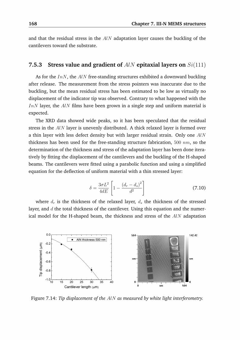
168 Chapter 7. III-N MEMS structures
and that the residual stress in the AlN adaptation layer causes the buckling of the
cantilevers toward the substrate.
7.5.3 Stress value and gradient of AlN epitaxial layers on Si(111)
As for the InN , the AlN free-standing structures exhibited a downward buckling
after release. The measurement from the stress pointers was inaccurate due to the
buckling, but the mean residual stress has been estimated to be low as virtually no
displacement of the indicator tip was observed. Contrary to what happened with the
InN layer, the AlN films have been grown in a single step and uniform material is
expected.
The XRD data showed wide peaks, so it has been speculated that the residual
stress in the AlN layer is unevenly distributed. A thick relaxed layer is formed over
a thin layer with less defect density but with larger residual strain. Only one AlN
thickness has been used for the free-standing structure fabrication, 500 nm, so the
determination of the thickness and stress of the adaptation layer has been done itera-
tively by fitting the displacement of the cantilevers and the buckling of the H-shaped
beams. The cantilevers were fitted using a parabolic function and using a simplified
equation for the deflection of uniform material with a thin stressed layer:
δ =3σL2
4dE
[1− (dr − ds)2
d2
](7.10)
where dr is the thickness of the relaxed layer, ds the thickness of the stressed
layer, and d the total thickness of the cantilever. Using this equation and the numer-
ical model for the H-shaped beam, the thickness and stress of the AlN adaptation
Figure 7.14: Tip displacement of the AlN as measured by white light interferometry.

7.6. Conclusions 169
layer have been determined. It has been estimated that a layer of ∼ 50 nm has a
residual tensile stress of 1 GPa, while the rest of the film is completely relaxed. This
is of course a rough approximation to the real stress distribution in the layer, that
empirically fits the measurement data. In reality a smooth evolution of the residual
stress is expected. However, what seems clear from the models is that a thin layer
close to the interface with the silicon has a large residual stress that is rapidly relaxed
moving in the z axis, leaving a thick layer of AlN under a low residual stress state.
7.6 Conclusions
Nitride semiconductor free-standing test structures have been fabricated for the
analysis and modeling of the main mechanical parameters for MEMS: flexural stiff-
ness, residual strain and stress gradient. The material elastic modulus has been mea-
sured and the stress distribution has been modeled in close agreement with the ob-
served data. It is also worth noting that the fabrication technology optimized in this
thesis, and already discussed in previous chapters, has been proven successful for
producing free-standing structures of high crystal quality epitaxially grown nitride
semiconductors.
The elastic modulus of the three main binaries of the III-N semiconductor system
has been measured. The value for the alloys can be interpolated using the Vegard’s
law from the three corner values, that are:
• EGaN ≈ 316 GPa
• EAlN ≈ 329 GPa
• EInN ≈ 137 GPa
The residual strain has been measured by XRD and the relaxation induced effects
have been studied and modeled using special free-standing test structures. The fit
of the developed models with the experimental data has been excellent for all the
materials: GaN , AlGaN/GaN , AlN and InN .
In the case of InN and AlN layers, it has been seen that the material is completely
relaxed and that the residual stress can be neglected in the design of the structures.
Nevertheless, for structures with asymmetric clampings, a small buckling toward the
substrate has been observed. The origin of this deformation has been modeled to
be related with a small adaptation layer that is formed on the silicon substrate. The
thickness of this layer is of few tenths of nanometers. In the case of the InN the

170 Chapter 7. III-N MEMS structures
adaptation layer is believed to be coincident with the AlN buffer layer grown on the
silicon for improving the nucleation and crystal quality of the InN . The stress of the
thin AlN adaptation film has been estimated to be between 750 MPa and 1 GPa.
On the contrary, for the GaN layer a large bulk residual stress has been found.
The mean stress value that has been measured is around 980 MPa (ε = 3.1 · 10−3).
Additionally, a severe out-of-plane buckling has been observed. The addition of a
layer with lower residual stress at the bottom of the structure was necessary for suc-
cessfully modeling the deformation of the structure. The stress of this layer has been
estimated to be 820MPa (ε = 2.6·10−3). The explanation for this stress distribution is
speculated to be a defect related relaxation of the lower GaN surface. These defects
are believed to be induced during the structure release. These observations were
made regardless of the GaN layer thickness and of the presence of a thin AlGaN
barrier. Therefore it is believed to be an intrinsic effect of the processing of GaN
free-standing structures.
Finally, an effect of the underetching of the clampings has also been observed.
The etching beneath the clampings induces a deformation on the asymmetrically
clamped structures. The deformation is due to the uneven stress relaxation because
of the different boundary conditions on the layer faces due to the ambient and the
substrate. This uneven relaxation produces an upward deformation of the structures,
in the case of tensile residual stress. This deformation is incremented if the clampings
are underetched, as the slope has been found to be proportional to the underetch
length, using the numerical model. This effect produces a large deformation of the
GaN asymmetric structures, together with the stress gradient generated during the
GaN growth. Therefore double clamped structures have to be used for the design of
GaN based MEMS structures. If a stress-free working point is required by the device
design, an H-shaped beam can be used as the simulations show a complete relaxation
of the central beam. Anyway, the deformation is low due to the stiffness of the two
longitudinal beams.

Chapter 8
Nanocrystalline diamond resonators
The technology developed in this thesis, described in the second part of this dis-
sertation, has been used to produce NCD free-standing structures that have been
statically and dynamically characterized. The characterization of these structures al-
lowed the determination of the mechanical parameters of the NCD layers as well as
the measurement of the resonator performance. The acquired knowledge was used
for modeling and designing more complex structures, described later in chapter 9.
8.1 Introduction and motivation
The intrinsic mechanical properties of diamond, such as its high Young’s modulus,
fracture strength, and low mass density [35], make diamond a perfectly suited mate-
rial for high frequency and harsh environment MEMS [251,252]. Depending on the
deposition conditions the mechanical properties of the NCD can be modified [45],
but when the grain size of NCD is larger than 50 nm the properties of this material
approach to those of the crystalline diamond [35]. The details on the superlative
properties of NCD have already been presented in the chapter 1.
NCD has been employed for the fabrication of RF switches [253] and several
types of resonators [53, 64, 254–256]. In these devices the outstanding mechani-
cal properties of diamond have been exploited to reach high resonant frequencies
(640 MHz [53]) and low switching times [251,253].
Other functioning principles have yielded very high frequency NCD resonators,
such as the disk resonator by Wang et al. [63], operating at 1.51GHz withQ = 11555.
In other published work, Gaidarzhy et al. [54] claim a cantilever type resonator fab-
ricated with NCD operating at frequencies as high as 1.441 GHz and a frequency-
quality factor product of Qf = 1013 Hz. In a recent work, Yang et al. [257] have
171

172 Chapter 8. Nanocrystalline diamond resonators
used ultrathin NCD layers (50 nm) for the fabrication of resonant membranes sus-
pended by two nanoscale tethers operating in torsional mode in the 10 MHz range,
with quality factors above 103. NCD has been also used in piezoelectrically actuated
devices [258], but this type of devices will be specifically addressed in chapter 9.
Finally, NCD can also be used for other type of sensors, such as gas sensors [259].
Extremely high quality factors have been reported for NCD beam resonators op-
erated at the MHz range at room temperature (∼ 10000) [260]. Other recent works
claim the fabrication of NCD resonant structures with Q = 28800 [261], although
this value is still far from the quality factor obtained for similar devices fabricated
with single crystal diamond (∼ 500000) [260]. Nevertheless, NCD is much easier to
produce, process and integrate with other materials. Consequently, NCD is the more
suitable material for functional MEMS from the carbon material family.
All these published results provide sufficient ground for claiming that NCD is an
excellent material for MEMS sensors and actuators fabrication for high frequency and
high Q applications. Moreover, the excellent thermal and chemical stability of NCD
allows the usage of the fabricated devices in harsh environment applications. Hence
the fabrication of NCD MEMS is one of the objectives in this thesis.
For a correct design of the device performance and the actuation principles, sim-
ple devices have to be fabricated and characterized in order to asses the material
properties and the performance limiting factors. At a later stage, the obtained knowl-
edge may be used for the design of complex structures. In this chapter this first
research step is addressed. Simple beam resonators have been fabricated for the
analysis of the material properties and device performance using magnetomotive ac-
tuation.
The technology developed in the previous part of this thesis was used for the
fabrication of metal/NCD free-standing structures. The structures were completely
covered by a Ti/Au/Ni (20 nm/100 nm/80 nm) metal stack that served as both
etch mask and current conductor for the magnetomotive actuation. Various NCD
materials have been used and the mechanical properties of the NCD and the resonant
structures have been calculated. Finally, behavioral models were derived for their use
in the design of more complex structures, which will be described in chapter 9.
8.2 Structure fabrication
Several structures have been fabricated to fulfill the objectives set for the NCD
resonator study. In this section the geometry and material used for the free-standing

8.2. Structure fabrication 173
structure fabrication process are presented and discussed. Additionally, the fabrica-
tion process steps are summarized, although the technological details have already
been discussed in chapters 3 and 4.
8.2.1 Free-standing structure description
A lithography mask was specially developed for this thesis. Different structures
were included on this mask. Stress characterization structures, etch resolution and
undercut control structures were added to the arrays of functional resonators. Three
types of functional structures have been fabricated:
1. Single clamped cantilevers
2. Double clamped beams
3. U-shaped resonators
The cantilever structures are simple rectangular beams clamped from one side
to the substrate. The structure is characterized by the length (L), width (w) and
thickness of the cantilever (d). The thickness of the cantilever is determined by the
material thickness and the width will be fixed to 4 µm for this dissertation. Several
arrays of cantilevers with variable length have been fabricated, with 10 µm ≤ L ≤200 µm. This structure has only one contact and cannot be excited by a current
as the circuit is not closed along the free-standing structure. Thus the cantilever
beams will only be used for static experiments as they cannot be measured using the
magnetomotive setup.
The double clamped structures are rectangular beams clamped to the substrate
on both sides. As for the cantilevers, the structure is characterized by the length
(L), width (w) and thickness of the cantilever (d), where d is given by the material
thickness and w has been fixed to 4 µm. Several arrays with variable length have
been fabricated, with L spanning from 20 µm to 500 µm. These structures have two
contacts, one at each clamping region, and can be tested using the magnetomotive
setup.
The U-shaped structure is a combination of two cantilever beams joined at their
free end by another transverse beam, see figure 8.1. This structure is characterized
by the length of the longitudinal beams (L), width of the beams (w), thickness of the
structure (d) and separation between the longitudinal beams (W ). The advantage of
this structure is that it provides two contacts but an asymmetric clamping that allows
the relaxation of the residual stress along the beam direction. Therefore, even with

174 Chapter 8. Nanocrystalline diamond resonators
Figure 8.1: U-shaped microstructures.
material under residual stress, the U-shaped structures provide a residual stress free
device. As for the other structures, d is given by the material thickness and w has
been fixed to 4 µm. Several arrays have been fabricated with L spanning from 20 µm
to 160 µm. Two different sets of U-shaped devices have been fabricated:
1. Narrow devices with W = L/2
2. Wide devices with W = L
Due to the existence of two contacts, the U-shaped beams can be measured using
the magnetomotive setup. An additional advantage exists for these devices. In fact, if
the in-plane magnetic field is directed perpendicularly to the transverse beam, when
the structure starts vibrating a spire effect will appear. When the longitudinal beams
deflect, the transverse beam is displaced out-of-the plane forming a square spire
normal to the magnetic field. This effect increases the susceptibility of the structure
to small displacements. Hence the resonance peaks provide larger reflections leading
to improved peak determination even for higher order modes.
All the structures have the clamping regions patterned in such a way that they
can be contacted using RF GSG probes. These probes are used by the magnetomotive
setup to provide the frequency variable excitation.
8.2.2 Resonator fabrication process
The fabrication process is simple and can be summarized in the following steps:
1. Deposition of NCD over a Si(001) substrate (described in the following subsec-
tion).

8.2. Structure fabrication 175
2. Deposition of metal etch mask. A Ti/Au/Ni (20 nm/100 nm/80 nm) stack is
used, as described at section 3.5.
3. Dry reactive ion etching of NCD in H2 : O2 plasma. The etching optimization is
described in section 3.5.
4. Overgrowth of Au (200 nm) over the Ti/Au/Ni metal stack for improving the
contact with GSG RF probes.
5. Dry sacrificial etching of the silicon substrate in SF6 plasma as described in
section 4.3.2.
The fabrication procedure was performed in the Fraunhofer IAF clean room using
a mask set specially developed for this thesis.
8.2.3 Material description
The structures described before were used for studying the properties of two NCD
materials. Moderate and low methane concentrations were used for the deposition
of these materials:
1. NCD film deposited over Si(001) with a 3% methane concentration and a thick-
ness of 300 nm
2. NCD film deposited over Si(001) with a 0.5% methane concentration and a
thickness of 140 nm
Both wafers were deposited at 830C in a H2 : CH4 plasma, following a stan-
dard deposition procedure described in [82]. The silicon wafers were seeded using
a monodisperse diamond colloid known to yield NCD nucleation densities above
1011 cm−2 [38]. AFM characterization showed a grain size around 70 nm and a sur-
face RMS roughness of approximately 20 nm. SEM inspection was used to verify the
excellent coalescence of the layers and to measure the thickness of the NCD. Raman
spectroscopy showed that the material was fundamentally formed by sp3 bonds but
a small amount of sp2 bondings were present at the grain boundaries [39]. Addition-
ally, a tensile residual stress was detected for the layer deposited with 0.5% methane
concentration, although the exact amount was not quantified.
The studied material properties were used for analyzing the performance of the
fabricated microstructures. In what follows, the Young’s modulus, mass density and
residual stress determination for these films is discussed. The obtained values will

176 Chapter 8. Nanocrystalline diamond resonators
be also used for developing analytical and numerical models of the performance of
resonators. The results and models developed in this chapter will be used in chapter 9
for the modeling and design of more complex structures.
8.3 Static determination of the mechanical properties
of NCD
The fabricated structures were characterized using the AFM force calibration
method described in section 2.6. These measurements are intended to obtain the
static elastic properties of the micromachined NCD. Both, double clamped and sin-
gle clamped structures were tested and the force calibration curves were fitted using
equations (2.12) and (2.13), respectively. The following structure sizes were selected
for the static mechanical characterization:
• Single clamped cantilevers with w = 4 µm and L from 10 µm to 30 µm
• Single clamped cantilevers with w = 4 µm and L from 10 µm to 40 µm
For accurately determining the Young’s modulus of the NCD, the metal mask was
removed. The metal was etched in HF (10%) and the structure was rinsed in iso-
propanol and placed in a furnace at 120C, in order to avoid stiction problems. SEM
inspection confirmed that the structures did not collapse after the metal layer re-
moval. As mentioned before, two different NCD layers were characterized:
• NCD grown with 3% methane concentration
• NCD grown with 0.5% methane concentration
8.3.1 Young’s modulus determination
The AFM force calibration curve measurement technique was used to measure
the Young’s modulus of free-standing NCD structures. The AFM cantilever tip was
calibrated as explained in section 2.6. In order to have a reliable calibration of the
elastic constant of the tip, long probes with a large contact area were selected. The
calibration was performed bending the tip as less as possible in order to ensure that
the indentation depth at the surface was small enough in order to be neglected in the
measurement postprocessing. It was verified that the cantilever suffered no degra-
dation during the measurements by measuring beyond the characterized structure
((x/L) > 1).

8.3. Static determination of the mechanical properties of NCD 177
The larger deflection of the single clamped cantilever structures provide a bet-
ter estimation of the Young’s modulus. Moreover, the absence of residual stress for
cantilever structures, as it gets completely relaxed by releasing the structure, makes
the interpretation of the measurements straightforward. Conversely, the fit of the
double clamped beams yields higher residuals due to the high stiffness of the NCD
structure. Besides, the direct measurement of the Young’s modulus of the material
can be affected by the stress stiffening effect if tensile residual stress is present in the
film.
Similar AFM characterization experiments have been performed for the mechan-
ical characterization of other materials. Several examples in the literature for mi-
cro and nanoscale structure mechanical characterization are given by [262–265].
This technique has been even applied for characterizing lung tissue [266] or cell nu-
cleus [267]. Very recently, this technique has been used for the determination of the
flexural rigidity of ultrathin diamond-like-carbon membranes [268].
For the characterization of the two materials under study, single clamped can-
tilevers and double clamped beams were measured for the NCD layer grown at higher
methane concentration. Unfortunately, due to processing issues only double clamped
structures were available for static mechanical characterization of the NCD deposited
with 0.5% methane concentration.
Results for the sample deposited with 3% methane concentration
For this material, single and double clamped structures were analyzed and the
values of Young’s modulus were extracted and averaged for both device types. The
separation of the statistics for both structures was done in order to identify a devia-
tion that could be attributed to residual stress in the NCD film. Indeed, if a residual
stress is accumulated in the NCD layer, the double clamped structure will not be ca-
pable of relaxing along the beam axis, and a modification of the measured Young’s
modulus will be detected. The exact geometry of every characterized structure was
measured by SEM, getting an NCD layer thickness of d = 300 nm.
The measurements of both structures provided very consistent values of E. The
large measured deflections, specially for the single clamped cantilever structures
yielded values of E with low residual fitting. The averaged values obtained for both
structures are
Ecantilever = 954± 38 GPa
Ebeam = 941± 43 GPa(8.1)

178 Chapter 8. Nanocrystalline diamond resonators
Figure 8.2: Determination of Young’s modulus of a NCD layer by AFM force calibrationcurves on single and double clamped free-standing structures.
The measurement fit with the obtained values is shown at figure 8.2. The ex-
cellent agreement of the fit to the measured data is observable. The values of E
calculated for the asymmetric and symmetric clamping structures indicate that the
residual stress in the layers is low and can be neglected for the elastic calculations.
Thus, a combined value can be calculated yielding ENCD = 947± 40 GPa.
The literature regarding the determination of the Young’s modulus of NCD by var-
ious techniques is extense [46,47,53,269–271]. The values obtained for these NCD
layer are high compared with other reported values. A complete characterization of
the dependence of the elastic properties of thin NCD films with growth conditions
was later performed by Dr. O. A. Williams et al. [45]. They show that the value ob-
tained by the AFM technique is completely coherent with the reported values at [45],
that were determined by measuring the deflection of membranes for various pressure
differences.
Results for the sample deposited with 0.5% methane concentration
For this material only double clamped beams were analyzed. The structures were
fabricated following the process described in section 8.2. The thickness of the layer
was measured by SEM inspection, d = 140 nm, as well as the exact magnitudes of
the geometrical parameters of the tested structures. The experiments were carried
out using a tip with kAFM ≈ 4.87 N/m.

8.3. Static determination of the mechanical properties of NCD 179
A very low deflection of the structure was measured even with such a low thick-
ness. An estimation of the Young’s modulus was extracted for the longer beams,
although the obtained value was much higher than 1100 GPa but with a very high
fit residual (ε > 200 GPa) caused by the uncertainty due to the low deflection. Such
high Young’s modulus could be obtained due to stress stiffening effect by a tensile
residual stress.
No single clamped beams were available for verifying this hypothesis. Neverthe-
less, measurements on resonators fabricated with this material will be discussed in
later sections. In fact, the dynamic measurements will show that the high values of
Young’s modulus measured with the AFM setup can be attributed to a stress stiffen-
ing effect caused by a large tensile residual stress accumulated in this NCD layer, as
described in section 8.4.
8.3.2 Metal layer stress determination
A large out-of-plane buckling of the single clamped structures, cantilevers and
U-shaped beams, has been observed after the sacrificial etching of silicon. This ef-
fect was larger specially for the sample grown with 3% methane, despite the met-
allizations and processes were equal for both NCD materials. The buckling may be
attributed to a stress gradient built up during growth or to a large tensile stress in
the metal layer.
The NCD material was optically characterized in collaboration with Dr. O. A.
Williams. It was expected that little or inexistent residual stress for the NCD grown
with 3% methane was expected, whereas a certain tensile stress for the NCD grown
with 0.5% methane was detected. The residual stress was not quantified because the
measurement objective was the assessment of peak existence and not the accurate
determination of their position.
After the removal of the metal layer in the wet etching procedure, it was ob-
served that the structures exhibited no out-of-plane buckling (figure 8.3). Hence, the
deformation of the single clamped structures is attributed to residual tensile stress in
the metal layer. The residual stress in the NCD material grown with 0.5% methane
reduced the gradient along the structures, and therefore the buckling.
The structures were measured before and after the metal layer removal by WLI in
order to asses the buckling displacement. The NCD material grown with 3% methane
was assumed to be fully relaxed, and the deformation was entirely attributed to an
uniform stress in the metal layer. The stress in the metal stack was determined using
a simplification of (7.9) for the deformation of a cantilever beam due to a stressed

180 Chapter 8. Nanocrystalline diamond resonators
Figure 8.3: SEM images of the deformation of NCD cantilever before (left) and after(right) the removal of the metal layer.
layer [250]:
∆z =3σL2
4dEd
[1− (d1 − d2)2
d2
](8.2)
where Ed is the volume average of the Young’s modulus of the metal/NCD mul-
tilayer, d1 is the thickness of the NCD film and d2 the thickness of the metal mul-
tilayer. For the Young’s modulus of materials the values were taken from [272],
ENi = 200 GPa and EAu = 78 GPa. The titanium adhesion layer was neglected
because it is very thin compared to the NCD roughness to produce any appreciable
effect. The Young modulus used for the NCD layer was the calculated value from the
AFM force calibration measurements. Using these values and (8.2), the tensile stress
in the metal layer was calculated to be
σm ≈ 490 MPa
Such large values may occur in evaporated metal thin layers deposited by evap-
oration. An early work analyzed the stress in metal layers deposited by evaporation
providing similar values for gold (σ ≈ 200 MPa for dAu = 100 nm) and even higher
for nickel (σNi ≈ 800 MPa for dNi = 80 nm) [273]. Thus, although the measured
value is high, similar residual stress has been reported for similar metal layers.
8.4 Dynamic characterization of NCD microdevices
In the previous section, the static determination of E of the deposited material
was done using the AFM force calibration curves. In this section, the characterization

8.4. Dynamic characterization of NCD microdevices 181
of NCD resonant structures is discussed. Double clamped beams and U-shaped struc-
tures have been characterized by means of the magnetomotive setup described in
section 2.6.2. The structures were fabricated using the NCD grown with 3% and
0.5% methane concentration. The layers deposited with 3% methane were thor-
oughly characterized and the discussion in this chapter will refer to these films. A
separate subsection is devoted to the results with NCD grown with 0.5% methane
concentration.
8.4.1 Previous considerations
The general equation for determining the flexural resonance frequencies is given
by
f0n = κn
√E
ρ
d
L2(8.3)
where the coefficients κn depend on the boundary conditions of the structure and
on the mode order (see appendix A for more details). In order to take into account
the effect of the metal/NCD multilayer, the above equation has to be reorganized as
follows:
f0n = 2√
3κn
√EI
µ
1
L2(8.4)
where I is the moment of inertia (given by I = wd3
12for a rectangular beam) and
µ the mass per unit length (µ = ρwd). In the above equation, the factor EI has to be
taken for the multilayer. In order to find the effective EI product, the position of the
neutral axis has to be calculated as [274]
zmm =Edd
2d + (2dd + dm) dmEm2 (ddEd + dmEm)
(8.5)
where dd and dm are the thicknesses of NCD and metal, respectively. The Young’s
modulus of the layers have been noted as Ed for NCD and Em for the metal layer. The
metal layer effective Young’s modulus has been calculated to be Em = 132 GPa as
described at section 8.3.2. Having determined the neutral axis position, the moment
of inertia of the layer i relative to the neutral axis is calculated using the parallel axis
theorem:
Ii =wd3i12
+ wdi (zi − zmm)2 (8.6)

182 Chapter 8. Nanocrystalline diamond resonators
where zi is the centroid of the layer (zd = dd/2 and zm = dd + dm/2). Finally, the
effective EI product is given using the Young’s modulus of each material pondered
by the moment of inertia of the layer,
EI = EdId + EmIm (8.7)
In what follows, the stress effect in the multilayer will be analytically character-
ized. Therefore, the model given by (8.3) has to be modified to take into account
the stress stiffening effect of the residual tensile stress that is not relaxed during the
mechanization of the structure. In order to asses the tensile stress stiffening effect on
the resonance frequency, the equation (8.3) is corrected by a term that depends on
the stress in the layer [275]
f0n = κn
√E
ρ
d
L2
√1 + γn
L
dε (8.8)
where ε is the longitudinal residual tensile strain in the beam, and the coefficients
γn depend on the considered mode shape
γn =12
L2
∫ L0
(∂u∂x
)2dx∫ L
0
(∂2u∂x2
)2dx
(8.9)
For a double clamped beam the coefficient of the fundamental mode is γ1 ≈ 0.295.
This model has been used for accurate determination of the residual strain in free-
standing structures [276].
8.4.2 Dynamic response of double clamped beams
The double clamped beam structures have been characterized using the magne-
tomotive setup at an ambient pressure of 5 · 10−5 mbar. These structures, when in
resonance, create out-of-plane lobes that act as a spire and induce a voltage. This
induced voltage causes the impedance of the RF setup to get out of balance and a
reflected wave appears, that is measured by the network analyzer used in the setup.
If the number of lobes in the beam is even, they are oriented in opposite direction
in the z axis, and the originated voltages are canceled. Therefore, for these struc-
tures only the fundamental mode and odd order overtones can be measured. For
the following discussion, the beams were measured in the linear vibration regimes,
whereas the non linear vibration regime is analyzed in a later subsection.
The measured data was fitted using the models given by (8.3) and (8.8). The

8.4. Dynamic characterization of NCD microdevices 183
Coefficient ValueEd 947 GPaEm 132 GPaρm 14.68 g/cm3
σm 490 MPa
Table 8.1: Material coefficients assumed for the analysis of the dynamic characterizationof double clamped beams.
material properties of the NCD film were calculated taking into account the effective
EI product due to the displaced neutral axis position. A numerical model was also
developed for fitting the data using ANSYS FEM software. The beam was modeled us-
ing the high order (20 nodes) structural SOLID95 elements with pre-stress and stress
stiffening capabilities. A Bloc-Lanczos spectral solver was used for the determination
of the resonance frequencies and mode shapes of the structures. The parameters in
table 8.1 have been used for the analytical and numerical calculations. These values
were extracted for the static characterization results and from [272].
The measured data has been shown in figure 8.4 together with the fits using the
different models. The analytical model fit at the lower frequency range is very good.
Nevertheless, a deviation for the shorter beams, specially notable for the fundamental
mode, has been found. The best fitting of the data was achieved using the analytical
Figure 8.4: Experimental and fitted data of the resonance frequencies of NCD doubleclamped beams measured in the magnetomotive setup.

184 Chapter 8. Nanocrystalline diamond resonators
model (8.8), adding a 490MPa tensile stress to the metal layer and 50MPa of tensile
stress to the NCD film. These stress values are coherent with the initial assumptions
based on the static characterization.
Nevertheless, the model fails for the shorter beams, overestimating the resonance
frequency. The FEM numerical model was adjusted using the calculated stress in
the layers and the measured material parameters. In order to asses all the possible
effects, the stress stiffening of the structure for large vibrations was considered and
the exact geometry, with the underetching at the clampings, was included in the
model. The results show an excellent agreement between the numerical model and
the measured data. The frequency deviation has been attributed to the effect of
the underetching at the clampings. This effect has been analyzed separately and
analytical approximation models are derived in section 8.6.
The material parameters of the NCD have been extracted from the fitting of
the analytical data. A high acoustic velocity has been derived for the NCD layer,√Eρ≈ 17283 ms−1. Using the value of Young’s modulus calculated from the static
mechanical characterization (947 GPa), the value of mass density is
ρd = 3.17± 0.15 g/cm3 (8.10)
This mass density is in agreement with those commonly found in the literature
[61,251,277], confirming the good quality of the deposited material. The appearance
of a seventh-order resonance peak is also indicative of the outstanding quality of the
NCD material. The FEM model confirms that the measured data corresponds to the
pure flexural z-directed odd modes. The large acoustic velocity also yields a high
resonant frequency, well above 1 MHz for devices made by using a standard optical
contact lithography technique.
The quality factor of the resonators was around 2200 due to the severe damping
imposed by the metal layer used for the actuation. The thickness of the metal is
comparable to that of the diamond, and, therefore, hinders the achievement of the
expected narrow bandwidth resonance peaks. A similar effect has been previously
reported by Sepulveda et al. [254] for electrostatic actuation schemes. They observed
that the damping produced by the metal leads to similar quality factor values. As
a result, a compromise has to be reached for the thickness of the metal layer: if
reduced, the quality factor is expected to improve, although the actuation force will
decrease significantly. A detailed study of the quality factor is addressed later in this
chapter.
If the obtained resonance frequencies are normalized by the effective geometric
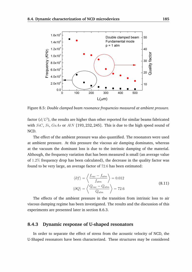
8.4. Dynamic characterization of NCD microdevices 185
Figure 8.5: Double clamped beam resonance frequencies measured at ambient pressure.
factor (d/L2), the results are higher than other reported for similar beams fabricated
with SiC, Si, GaAs or AlN [193, 232, 245]. This is due to the high speed sound of
NCD.
The effect of the ambient pressure was also quantified. The resonators were used
at ambient pressure. At this pressure the viscous air damping dominates, whereas
at the vacuum the dominant loss is due to the intrinsic damping of the material.
Although, the frequency variation that has been measured is small (an average value
of 1.2% frequency drop has been calculated), the decrease in the quality factor was
found to be very large, an average factor of 72.6 has been estimated:
〈∂f〉 =
⟨fvac − fatm
fatm
⟩= 0.012
〈∂Q〉 =
⟨Qvac −Qatm
Qatm
⟩= 72.6
(8.11)
The effects of the ambient pressure in the transition from intrinsic loss to air
viscous damping regime has been investigated. The results and the discussion of this
experiments are presented later in section 8.6.3.
8.4.3 Dynamic response of U-shaped resonators
In order to separate the effect of stress from the acoustic velocity of NCD, the
U-Shaped resonators have been characterized. These structures may be considered

186 Chapter 8. Nanocrystalline diamond resonators
Figure 8.6: Experimental and fitted data of the resonance frequencies of NCD U-shapedresonators measured in the magnetomotive setup.
as two single-clamped cantilever beams coupled by a third transverse beam which
closes the frame. The asymmetric clamping of the frame favors the relaxation of
the residual stress in the metal layer through out-of-plane bending. As a result,
the resonance frequency of such structures is expected not to be affected by stress
stiffening effects. Therefore, a better fit and a more accurate material parameter
extraction is possible, making the characterization of these asymmetrically clamped
structures not an idle exercise.
As mentioned above, the structure is used as a spire for a more efficient driv-
ing; consequently, the electrical power applied to the actuation metal layer required
to obtain a measurable resonance peak was more than 20 dBm lower than for the
double-clamped beams. Two different U-frame geometries were tested where the
separation between the coupled cantilever beams was equal (W = L) or half to their
length (W = L/2), respectively. For each one, the frequency of two resonance modes
(first and third) are represented in figure 8.6. It is observed that the fit to the numer-
ical model is excellent even for frequencies below the KHz range without including
any residual stress effect.
As expected, the stress stiffening effect observed in the double-clamped devices
is no longer present in these structures. This is because the residual stress is mostly
relieved through bending and the applied excitation is much lower. Therefore, the

8.4. Dynamic characterization of NCD microdevices 187
Figure 8.7: First to mode shapes of the U-shaped resonators with W = L (up) andW = L/2 (down).
stress at the clamping regions is kept below the value sufficient to observe a frequency
increase due to stress stiffening.
From the fit to the numerical model, which incorporates the effect of the under-
etched region at the clamping boundary on the resonance frequency, the acoustic
velocity of the NCD layer has been calculated to be 17174 ± 46 ms−1. This value is
very close to the value obtained for the double clamped beams using both the un-
stressed analytical and numerical model. Thus, these structures confirm the high
acoustic velocity of the NCD material. The excellent agreement of he data extracted
for both structures also validates the stress characterization performed for the double
clamped beams.
The modal analysis of the structures reveals that the variation of the length of the
transverse beam changes the frequency order of the overtones. As a result, the mea-
sured relation between the fundamental model and the overtones is not the same
for the narrow and wide resonators. The numerical solution reveals that the first
overtone of the narrow structure corresponds to the second flexural mode of the
longitudinal beams and no vibration of the transverse beam. Conversely, the first
overtone of the wide structure corresponds to the first flexural mode of the longitu-
dinal and transverse beams. Nevertheless, for both structures the fundamental mode
corresponds to the first flexural mode of the longitudinal beams. The configuration
of these resonators allows the measurement of the even modes of the beams due to
the spire effect.
The quality factor of the measured resonant peaks was found to be very similar to

188 Chapter 8. Nanocrystalline diamond resonators
Figure 8.8: U-shaped beams resonance frequencies measured at ambient pressure.
the observed for the double clamped beams, around 2000. The value of Q confirms
the intrinsic limitation of the quality factor, that has been attributed to dissipation
in the metal layer. Finally, the structures were also measured at ambient pressure to
produce the same behavior than the double clamped beams, as seen in (8.11):
〈∂f〉 =
⟨fvac − fatm
fatm
⟩= 0.05
〈∂Q〉 =
⟨Qvac −Qatm
Qatm
⟩= 64
(8.12)
Virtually no frequency shift has been measured, but a large quality factor drop
has been detected. As mentioned before, the influence of ambient pressure on the
quality factor is discussed later in section 8.6.3.
8.4.4 Nonlinear effects
The linear vibration model is an approximation that is only accurate for small
displacements. As the displacement becomes large, the higher order terms become
non negligible and introduce new solutions to the differential equations that turns
nonlinear. The nonlinearity leads to jumps in the frequency and force response curves
in the form of bifurcations [278].
In particular, if the vibration amplitude becomes large the nonlinear effects curves
the frequency response either to the right or to the left. The reason is that if the am-

8.4. Dynamic characterization of NCD microdevices 189
Figure 8.9: Double clamped beam under nonlinear vibration (left) and critical excitationpower (right).
plitude is increased beyond a critical point, a bifurcation point appears on the van der
Pol plane of the solutions to the differential equation [279]. The jump frequencies
determine the nonlinear behavior of the resonators. The well known model account-
ing on these phenomena is a called the Duffing model. A derivation of the Duffing
model and a general presentation of the various solutions may be found at [279]. For
the use of the Duffing model for analyzing beam and plate vibration, with a detailed
formula derivation, the interested reader may refer to [280].
The frequency bifurcation appears for an amplitude above a critical threshold
[280] given by
acr ≈32.896
L3πd
√E
ρ
√1.28πd
√E/ρ
3√
3
õ
|α|µ (8.13)
where α is the anharmonic term and µ is a damping related term given by the
product of the viscous damping and the natural resonance frequency (µ = ζωn). The
anharmonic term is composed by a positive, geometry related, hardening component
and a negative, inertia related, softening component [281]. In this term, the geo-
metrical hardening takes into account the stress stiffening that happens due to large
displacements. The sign of the anharmonic term, given by the geometric and inertia
term balance, determines the sense of the frequency bending. If the nonlinear be-
havior is dominated by the structure hardening, the resonance peak turns to higher
frequencies and, if it is dominated by inertia nonlinearity, the peak turns to lower
frequencies [280].
Other derivations of the nonlinear behavior of beams have been published at
[282,283]. The nonlinear analysis has been applied to the characterization of piezo-
electric composite beams [284] and energy harvesters [285].
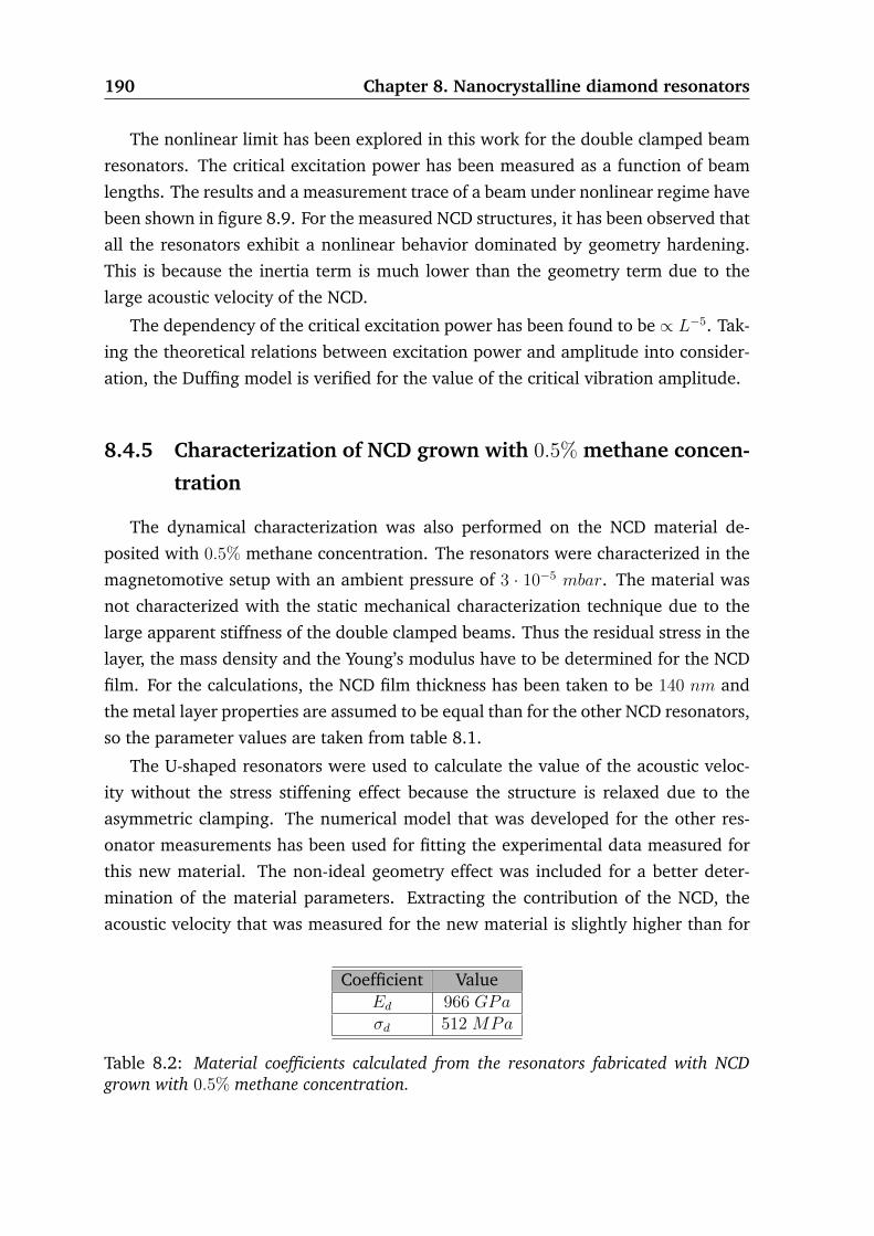
190 Chapter 8. Nanocrystalline diamond resonators
The nonlinear limit has been explored in this work for the double clamped beam
resonators. The critical excitation power has been measured as a function of beam
lengths. The results and a measurement trace of a beam under nonlinear regime have
been shown in figure 8.9. For the measured NCD structures, it has been observed that
all the resonators exhibit a nonlinear behavior dominated by geometry hardening.
This is because the inertia term is much lower than the geometry term due to the
large acoustic velocity of the NCD.
The dependency of the critical excitation power has been found to be ∝ L−5. Tak-
ing the theoretical relations between excitation power and amplitude into consider-
ation, the Duffing model is verified for the value of the critical vibration amplitude.
8.4.5 Characterization of NCD grown with 0.5% methane concen-
tration
The dynamical characterization was also performed on the NCD material de-
posited with 0.5% methane concentration. The resonators were characterized in the
magnetomotive setup with an ambient pressure of 3 · 10−5 mbar. The material was
not characterized with the static mechanical characterization technique due to the
large apparent stiffness of the double clamped beams. Thus the residual stress in the
layer, the mass density and the Young’s modulus have to be determined for the NCD
film. For the calculations, the NCD film thickness has been taken to be 140 nm and
the metal layer properties are assumed to be equal than for the other NCD resonators,
so the parameter values are taken from table 8.1.
The U-shaped resonators were used to calculate the value of the acoustic veloc-
ity without the stress stiffening effect because the structure is relaxed due to the
asymmetric clamping. The numerical model that was developed for the other res-
onator measurements has been used for fitting the experimental data measured for
this new material. The non-ideal geometry effect was included for a better deter-
mination of the material parameters. Extracting the contribution of the NCD, the
acoustic velocity that was measured for the new material is slightly higher than for
Coefficient ValueEd 966 GPaσd 512 MPa
Table 8.2: Material coefficients calculated from the resonators fabricated with NCDgrown with 0.5% methane concentration.
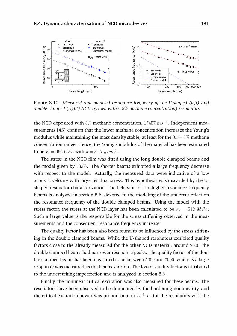
8.4. Dynamic characterization of NCD microdevices 191
Figure 8.10: Measured and modeled resonance frequency of the U-shaped (left) anddouble clamped (right) NCD (grown with 0.5% methane concentration) resonators.
the NCD deposited with 3% methane concentration, 17457 ms−1. Independent mea-
surements [45] confirm that the lower methane concentration increases the Young’s
modulus while maintaining the mass density stable, at least for the 0.5−3% methane
concentration range. Hence, the Young’s modulus of the material has been estimated
to be E = 966 GPa with ρ = 3.17 g/cm3.
The stress in the NCD film was fitted using the long double clamped beams and
the model given by (8.8). The shorter beams exhibited a large frequency decrease
with respect to the model. Actually, the measured data were indicative of a low
acoustic velocity with large residual stress. This hypothesis was discarded by the U-
shaped resonator characterization. The behavior for the higher resonance frequency
beams is analyzed in section 8.6, devoted to the modeling of the undercut effect on
the resonance frequency of the double clamped beams. Using the model with the
stress factor, the stress at the NCD layer has been calculated to be σd = 512 MPa.
Such a large value is the responsible for the stress stiffening observed in the mea-
surements and the consequent resonance frequency increase.
The quality factor has been also been found to be influenced by the stress stiffen-
ing in the double clamped beams. While the U-shaped resonators exhibited quality
factors close to the already measured for the other NCD material, around 2000, the
double clamped beams had narrower resonance peaks. The quality factor of the dou-
ble clamped beams has been measured to be between 5000 and 7000, whereas a large
drop in Q was measured as the beams shorten. The loss of quality factor is attributed
to the underetching imperfection and is analyzed in section 8.6.
Finally, the nonlinear critical excitation was also measured for these beams. The
resonators have been observed to be dominated by the hardening nonlinearity, and
the critical excitation power was proportional to L−5, as for the resonators with the

192 Chapter 8. Nanocrystalline diamond resonators
relaxed NCD. Nevertheless, the threshold for the critical excitation was found to be
lower. This difference is attributed to the residual stress in the layer that allows
smaller vibration amplitudes before the geometry nonlinearity affects the resonance
frequency.
As stated before, the values measured for these resonators are in accordance with
the values reported in the literature measured by other techniques [45]. The high
calculated Young’s modulus is an indicative of the excellent quality of the NCD ma-
terial. The effect of the residual stress allows the design of the resonators so the
frequency response and quality factor can be tuned.
8.5 Simulation and modeling
The data obtained from the static and dynamic characterization of the NCD res-
onators was used to develop models in order to fit the experimental data. These
models have already been discussed in the previous sections. It was shown that a
very good fitting of the experimental data was obtained.
These models have been used for exploring the limit values of the resonator de-
sign in order to identify the limiting factors for fabricating ultra high frequency res-
onators. A numerical FEM model was developed in ANSYS using the high order
structural SOLID95 element. The double clamped beam NCD resonator geometry
was simulated with the following parameters:
• Beam length from 0.5 to 5 µm
• Beam width from 0.1 to 0.5 µm
• Metal to NCD thickness ratio from 0.5 to 0.1
• Undercut length from 0.4 to 0.2 µm
The results show that a frequency limit around 1 GHz exists for this resonator
topology with the material parameters measured in the previous sections. The ob-
tained curves are shown in figure 8.11, where the frequency limit is clearly identifi-
able.
The effect of the different parameters on the resonance frequency can be ana-
lyzed separately. As expected, the frequency is increased as the metal thickness is
decreased. The reduction of the material with low E drives the position of the neu-
tral axis near the centroid of the NCD beam increasing the effective EI of the struc-

8.5. Simulation and modeling 193
Figure 8.11: Frequency limit simulations for double clamped NCD beam resonators.
ture. Unfortunately, the metal layer cannot be completely suppressed as a 1 GHz
frequency current has to circulate through the structure.
Additionally, other limiting factor that has been found for the high frequency
operation is the w/d ratio. As the width of the beam structure gets smaller, the
Euler-Bernoulli assumptions turn invalid and the normal planes to the neutral axis
get deformed, leading to the Timoshenko beam model. This deformation introduces
Figure 8.12: Effect of the metal thickness (left) and width to thickness ratio (right) onthe resonance frequency of double clamped beams.

194 Chapter 8. Nanocrystalline diamond resonators
Figure 8.13: Simulated effect on the resonance frequency of the underetch length.
a stiffening of the structure which leads to an increase of the resonance frequency.
This increment has been observed on the numerical model, which for small widths
follows a√d/w law, as shown in figure 8.12.
Finally, a critical effect of the underetch length has been found. This effect has
also been experimentally observed during the dynamic characterization of beams.
When the length of the beam approaches the underetch length at the clampings,
the frequency deviates from the theoretical curve. The effect of the underetching at
the clamping regions will be separately analyzed in the following section where an
analytical approximate model will be derived.
On the whole, for increasing the frequency of beam resonators the following de-
sign rules have to be considered:
• Reduce the metal thickness as much as possible. The limiting factor of this
reduction is the increment in resistivity that could hinder high frequency oper-
ation or lead to self heating issues.
• Reduction of the w/d ratio.
• Reduction of the underetching at the clamping region.
All of these three rules yield a stiffening of the structure. The decrease of the
underetch length and the reduction of metal thickness will also reduce the mechan-
ical losses of the resonator, thus increasing the quality factor of the resonance peak.
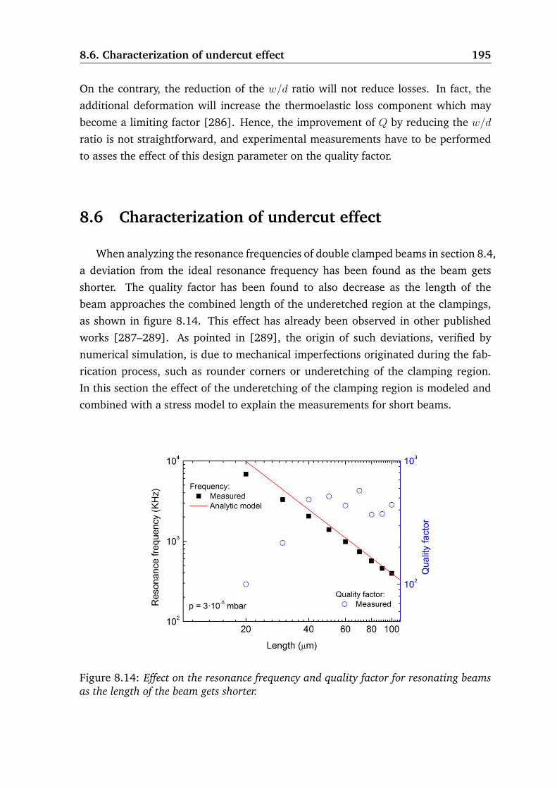
8.6. Characterization of undercut effect 195
On the contrary, the reduction of the w/d ratio will not reduce losses. In fact, the
additional deformation will increase the thermoelastic loss component which may
become a limiting factor [286]. Hence, the improvement of Q by reducing the w/d
ratio is not straightforward, and experimental measurements have to be performed
to asses the effect of this design parameter on the quality factor.
8.6 Characterization of undercut effect
When analyzing the resonance frequencies of double clamped beams in section 8.4,
a deviation from the ideal resonance frequency has been found as the beam gets
shorter. The quality factor has been found to also decrease as the length of the
beam approaches the combined length of the underetched region at the clampings,
as shown in figure 8.14. This effect has already been observed in other published
works [287–289]. As pointed in [289], the origin of such deviations, verified by
numerical simulation, is due to mechanical imperfections originated during the fab-
rication process, such as rounder corners or underetching of the clamping region.
In this section the effect of the underetching of the clamping region is modeled and
combined with a stress model to explain the measurements for short beams.
Figure 8.14: Effect on the resonance frequency and quality factor for resonating beamsas the length of the beam gets shorter.

196 Chapter 8. Nanocrystalline diamond resonators
8.6.1 Undercut effect modeling
For analyzing the effect of the undercut, a variable geometry model for the double
clamped beam has been analyzed to find an approximation to the observed behavior.
The variable width beam model modeling is similar to the method followed in [288,
290]. The total length of the resonant structure, depicted in figure 8.15, is
L = L1 + 2L0 (8.14)
where L1 is the length of the beam and L0 is the underetched length at each of
the clamping region, as observed in figure 8.15. The clamping region is considered
to be equivalent to a thin plate that verifies the Euler-Bernoulli assumptions (see
appendix A), and the displacement equation is given by
∂4u
∂x4+ 2
∂4u
∂x2∂y2+∂4u
∂y4=
q
D(8.15)
where D is the plate flexural rigidity given by
D =Ed3
12(1− ν)(8.16)
In this model the assumption w2< L0 < w is made, which allows considering that
in a region −ε < y < ε the displacement is independent of y. Thus the analysis can
be carried out reduced to the central longitudinal fiber of the beam. Then, the one
dimensional displacement model of the plate, for each clamping region, is reduced
to
∂4u
∂x4=q1DD
(8.17)
Figure 8.15: Geometrical model for the analysis of the underetching at the clampings.

8.6. Characterization of undercut effect 197
To convert the load to the one dimensional model it is divided by w arriving to
∂4u
∂x4=
qEwd3
12(1−ν)
(8.18)
The equation (8.18) is analogous to the Euler-Bernoulli equation (A.1) but in-
cluding the equivalent width
weq =w
1− ν(8.19)
The displacement equation of a beam under uniform loading (A.5) is extended to
both underetched clamping regions for the analysis:
u = A[x4 − 2Lx3 + L2x2
]sin (ωt+ φ) ; 0 ≤ x ≤ L (8.20)
The equivalent width (8.19) is used in the energy balance equation (A.6) for de-
termining the frequency of the fundamental resonance mode using the Ritz-Rayleigh
method. Solving the equations leads to
f01 ≈ κ1
√E
ρd√
72νL50 − 180νL1L4
0 + 160νL21L
30 − 60νL3
1L20 + 10νL4
1L0 + (1− ν)L51
140νL90 − 630νL1L8
0 + 1080νL21L
70 − 840νL3
1L60 + 252νL4
1L50 + (1− ν)L9
1
(8.21)
A finite element model has been developed using ANSYS with SOLID185 and
SOLID95 elements with L0 = w/2. The low and high order elements led to the same
results, so no distinction will be made in the discussion. The fundamental resonance
mode was analyzed, although the equation (8.21) was found not to yield a good
agreement with the numerical model.
To solve this deviation, the mode shape of the beam with underetched clampings
was analyzed. Figure 8.16 shows the numerical solution of the mode shape and the
approximations using (8.20) with different efficient length. It is seen that the mode
shape can be modeled extending the uniformly loaded displacement equation using
Le = L1 + L0.
Plugging this approximation into the energy balance equation leads to the funda-
mental mode approximation
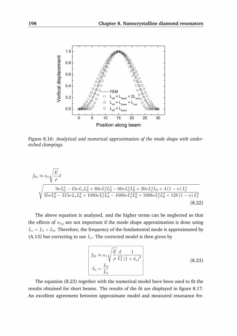
198 Chapter 8. Nanocrystalline diamond resonators
Figure 8.16: Analytical and numerical approximation of the mode shape with under-etched clampings.
f01 ≈ κ1
√E
ρd√
9νL50 − 45νLeL4
0 + 80νL2eL
30 − 60νL3
eL20 + 20νL4
eL0 + 4 (1− ν)L5e
35νL90 − 315νLeL8
0 + 1080νL2eL
70 − 1680νL3
eL60 + 1008νL4
eL50 + 128 (1− ν)L9
e
(8.22)
The above equation is analyzed, and the higher terms can be neglected so that
the effects of weq are not important if the mode shape approximation is done using
Le = L1 +L0. Therefore, the frequency of the fundamental mode is approximated by
(A.13) but correcting to use Le. The corrected model is then given by
f01 ≈ κ1
√E
ρ
d
L21
1
(1 + δu)2
δu =L0
L1
(8.23)
The equation (8.23) together with the numerical model have been used to fit the
results obtained for short beams. The results of the fit are displayed in figure 8.17.
An excellent agreement between approximate model and measured resonance fre-
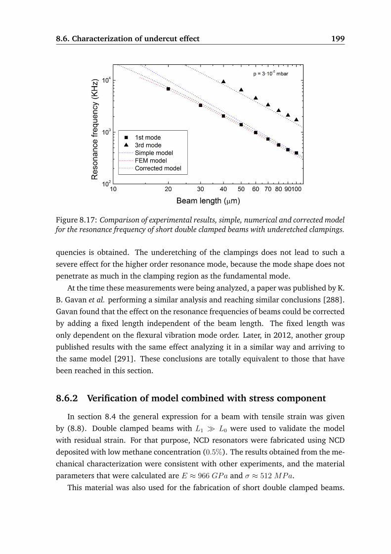
8.6. Characterization of undercut effect 199
Figure 8.17: Comparison of experimental results, simple, numerical and corrected modelfor the resonance frequency of short double clamped beams with underetched clampings.
quencies is obtained. The underetching of the clampings does not lead to such a
severe effect for the higher order resonance mode, because the mode shape does not
penetrate as much in the clamping region as the fundamental mode.
At the time these measurements were being analyzed, a paper was published by K.
B. Gavan et al. performing a similar analysis and reaching similar conclusions [288].
Gavan found that the effect on the resonance frequencies of beams could be corrected
by adding a fixed length independent of the beam length. The fixed length was
only dependent on the flexural vibration mode order. Later, in 2012, another group
published results with the same effect analyzing it in a similar way and arriving to
the same model [291]. These conclusions are totally equivalent to those that have
been reached in this section.
8.6.2 Verification of model combined with stress component
In section 8.4 the general expression for a beam with tensile strain was given
by (8.8). Double clamped beams with L1 L0 were used to validate the model
with residual strain. For that purpose, NCD resonators were fabricated using NCD
deposited with low methane concentration (0.5%). The results obtained from the me-
chanical characterization were consistent with other experiments, and the material
parameters that were calculated are E ≈ 966 GPa and σ ≈ 512 MPa.
This material was also used for the fabrication of short double clamped beams.

200 Chapter 8. Nanocrystalline diamond resonators
Figure 8.18: Model fitting of experimental results for the resonance frequency of shortdouble clamped beams with underetched clampings and large residual tensile strain. Thecurves for the simple Euler-Bernoulli model and the simple model with strain correctionhave been added for the first mode for comparison.
A large deviation from (8.8) is observed at the short beam range. The equivalent
length Le = L1 + L0 was used to modify the stress correcting factor but not for the
γ1 coefficient. This is justified by the fact that γ1 integrates the extended mode shape
over the efficient beam length and is thus not affected by the length correction.
Combining both correcting terms a complete model for the double clamped beam
with tensile strain and underetched clampings is given by the equation
f0n ≈ κn
√E
ρ
d
L21
1
(1 + δun)2
√1 + γn
(1 + δun)2 L21
d2ε (8.24)
where δu1 = L0/L1. The equation (8.24) has been used to fit the experimental
data measured with the magnetomotive response equipment. The results shown in
figure 8.18 demonstrate an excellent agreement between the complete model and
the measured resonance frequencies.
The model given by (8.24) has proven to be a very useful tool. The results shown
at figure 8.18 were first interpreted as the result for a material with low E and an
enormous residual strain. However, this interpretation was puzzling as it was not
coherent with the results obtained from the optical characterization of the NCD and
from the resonance frequency of single clamped U-shape structures. Nonetheless,

8.6. Characterization of undercut effect 201
incorporating the newly derived model solved the problem and provided a fully co-
herent explanation of all the measured data with excellent fit between model and
experiment.
8.6.3 Effect on the quality factor
A drop of the quality factor has been observed for the resonance peaks in the
region were the undercut effect causes deviations from the standard model. The
measurements for the loss mechanism determination were performed at an ambient
pressure of p = 3 · 10−5 mbar in order to ensure that the dominating loss mechanisms
are the intrinsic losses [292,293].
The low stress and large tensile stress NCD (grown with 3% and 0.5% CH4 respec-
tively) were analyzed. The resonators with low residual stress are clearly dominated
by the support loss mechanism [294, 295], while the resonators with high tensile
stress are dominated by a combination of surface and support losses. In both cases
the thermoelastic loss component in the NCD has been neglected, as it has been esti-
mated to be more than one order of magnitude above the measured Q figure [286],
due to the high thermal conductivity and low thermal expansion coefficient of NCD,
but it can be large for the metal layer.
The effect of the underetching of the clamping region is that the support loss term
is modified and introduces a large Q decay as L decreases. The values measured for
the pre-stressed resonators provide larger quality factors due to the stress stiffening
effect, but decay faster due to the larger undercut of the clamping region of 7 µm,
whereas the relaxed beams have only 4 µm of underetching at the clampings. Con-
Figure 8.19: Underetch at the clamping region effect on the quality factor of beamresonance. An example of a measurement used for Q determination is shown on the leftwheres on the right the measured Q versus beam length for two samples with differentL0 is shown.

202 Chapter 8. Nanocrystalline diamond resonators
sequently, the decrease in Q has been found to be faster if the underetching of the
clampings is bigger. The measured data, together with an example trace used for Q
determination, are shown in figure 8.19. The quality factor drop as the length of the
double clamped shortens evidences that for both materials the most prominent effect
is that of support losses, enhanced by the underetching, as the surface losses are less
sensible to L [296].
8.7 Characterization of ambient pressure effect
The resonance frequency of the double clamped structures have been analyzed in
order to identify the mechanism limiting the quality factor of the structures and to
estimate the critical pressures where the transition of dominant mechanism occurs.
As the pressure is increased, the quality factor turns from intrinsic limiting region
to a transition region where the molecular damping dominates and ends in the vis-
cous regime. The quality factor of the molecular and viscous region depends on the
geometry and measurement pressure, following the trend given by [297]:
Qmolecular ∝d2
L2p
Qviscous ∝
√d3
p
1
(1 + w)
(8.25)
where p is the measurement pressure.
The dependence of the quality factor of NCD with the ambient pressure has been
recently studied by Santos et al. [298]. Santos claims that, at the intrinsic pressure
regime, Q is limited by thermoelastic losses for long beams and by support losses
Figure 8.20: Resonance peak evolution with ambient pressure (left) and Lorentzian fit(right) used for Q determination of double clamped beams.

8.8. Conclusions 203
Figure 8.21: Evolution of quality factor with measurement pressure for resonators withlow and high intrinsic Q.
for shorter beams. As the pressure is increased, the structures with high quality
factor (longer beams) enter the molecular regime at the critical pressure. The critical
pressure is higher for the shorter beams because the intrinsic quality factor is lower,
and the crossing point with the molecular loss is produced at higher pressures. In
fact, Santos et al. claim that for structures with very low intrinsic quality factor, the
transition from intrinsic to viscous regime is produced without passing through the
molecular regime.
For the measured double clamped beams, a transition regime between intrinsic
and viscous losses has been observed for all the structures, regardless of the intrinsic
quality factor. This regime is found for the 0.01 − 1 mbar range. Final Q values in
the range of 102 have been measured, which is consistent with a viscous dominated
damping. The critical pressure, at which the transition region begins, variated from
0.005 mbar for beams with higher intrinsic Q (Q = 5100) to 0.01 mbar for beams
with lower Q, Q = 560. This change of the critical pressure is due to the interception
of the transition regime for lower pressures when the intrinsic Q is large [298].
Nevertheless, the transition regime has not been observed to vary proportionally to
p−1 as expected for a molecular limited regime. This discrepancy is probably due to
the influence of the metal layer that provides additional damping, driving the critical
pressure to lower values.
8.8 Conclusions
In this chapter the fabrication and characterization of NCD free-standing struc-
tures has been presented and discussed. The technology developed in the previous
chapters has been successfully employed for the fabrication of functional NCD res-

204 Chapter 8. Nanocrystalline diamond resonators
onators. The structures have been measured in order to extract the NCD material
parameters and identify the performance limiting factors that have to be optimized
for the fabrication of high performance NCD MEMS. In this study, NCD material
grown with 3% and 0.5% methane concentration have been analyzed.
Two different kinds of resonators have been fabricated, one with complete resid-
ual stress relaxation and other with symmetric clamping for analyzing the stress stiff-
ening effects on the resonator performance. Additionally, single clamped cantilevers
have been fabricated for the assessment of the NCD Young’s modulus. The com-
bined static and dynamic characterization lead to the determination of the Young’s
modulus, residual stress and mass density of the NCD material:
Property 3% CH4 0.5% CH4
ENCD 947 GPa 966 GPa
σNCD 50 MPa 512 MPa
ρNCD 3.19 g/cm3 3.17 g/cm3
These values are comparable to the best published values for thin NCD films and
coherent with the values measured with other techniques for equivalent material
[45].
The dynamic characterization of the resonators rendered resonance frequencies
up to 1 MHz for the fundamental mode. The good quality of the material was
evident by the measurement of the seventh order flexural mode. The quality factors
of the resonators, although high, were limited by the thick metal layer, that has been
measured to have a large residual tensile stress, σm = 490 MPa. This large residual
stress together with the poor elastic properties of the metal are responsible for the
quality factor loss, as published for other resonators by other authors [254].
Analytical and numerical models with incorporated stress effects have been de-
veloped, and they allowed to provide good fitting of the experimental data. These
models were used to explain the measurements of both resonator types for stressed
an relaxed NCD films.
The resonators were measured in the linear and nonlinear regime. The nonlinear
behavior of the resonators has been observed to be dominated by hardening effects
of the material. The resonance frequency bifurcation that has been measured is
consistent with the vibration pattern predicted by the Duffing model. The critical
amplitude of the resonance was not determined, but the critical excitation power
was measured in accordance with the nonlinear model.
The developed numerical models were used for exploring the design limits of the
double clamped beam NCD resonator performance. A limit frequency of 1 GHz for

8.8. Conclusions 205
this topology, working in the out-of-plane flexural mode with magnetomotive excita-
tion, has been identified. For higher resonator frequency other functional principles
should be used, such as acoustic wave confinement [63]. The frequency limiting
factors that have been discovered are:
• The metal layer thickness has to be reduced as much as possible. The limit to
the metal thickness is imposed by the RF requirements.
• The width to thickness ratio. A stiffening effect has been detected when the
w/d ratio is reduced. For increasing the resonance frequency the w/d shall be
reduced.
• The undercut of the clamping region has to be reduced as much as the technol-
ogy allows.
An analytical approximation for modeling the underetch imperfection has been
derived. The proposed model was modified to include the stress stiffening effect
due to tensile residual stress. The proposed model has been verified with the nu-
merical model and with experimental data measured for stressed and relaxed NCD
resonators. It has been proven that the inclusion of the underetch effect can be mod-
eled by using an effective length, larger than the beam length, that is given by the
resonant mode order.
Finally, the quality factor of the resonator has also been investigated. The intrinsic
quality factor of the resonator was measured in vacuum. It has been found that the
quality factor is severely affected by the damping in the metal layer. Nevertheless,
for short beams the limiting factor turns to be the losses at the support, aggravated
by the effect of the underetching imperfection at the clamping region. A transition
pressure range was observed when increasing the measurement pressure. This tran-
sition region deviates from the predicted molecular damping behavior [298] because
of what is believed to be an influence of the stressed metal layer. At ambient pressure
the quality factor is dominated by the well known viscous air damping.
On the whole, MEMS NCD structures were fabricated and the limiting perfor-
mance factors and material parameters were determined. The worthy knowledge
acquired by the work discussed in this section enables the development of precise
models for the design and performance prediction of more complex structures, which
are discussed in chapter 9.


Chapter 9
MEMS design and simulation
As previously discussed in other chapters of this dissertation, the NCD and III-N
materials enable the development of novel MEMS devices with high performance.
For this reason, in this final chapter the results obtained from the work described in
the previous chapters are exploited for the design and simulation of various MEMS
devices.
As an application of NCD MEMS devices, two structures will be explored. For the
actuation of these structures, piezoelectric AlN based integrated transducers have
been chosen to provide standalone actuation and sensing. In fact, a polycristalline
AlN actuator can be deposited on the NCD by reactive sputtering in order to form
the integrated actuator, If the back surface of NCD is used or the upper surface is
polished. Only a thin metal electrode is required for the actuation, as the low con-
ductivity of AlN limits the loss current to extremely low values, and the NCD can be
doped in order to provide an efficient grounding to the transducer without losing its
excellent mechanical properties. The AlN/NCD devices that have been studied are
of two types: beams and membranes.
• AlN/NCD beams. The piezoelectric actuation of single and double clamped
beams is studied, and the field emission switches design is discussed as an
application case.
• AlN/NCD membranes. The modifications on the optimal piezoelectric trans-
ducer imposed by the membrane axial symmetry are studied. NCD tunable
microlenses are designed as a case of application of the AlN/NCD membrane-
based devices.
In addition, the III-N system has also been used for producing high quality single
crystal MEMS, as discussed in chapter 7. The mechanical properties and stress mod-
207

208 Chapter 9. MEMS design and simulation
eling in the layers can be used for designing various devices. As a case of study we
have chosen:
• GaN/air electrostatically tunable optical cavity. The device is based on two
GaN membranes that are moved in order to modify the optical cavity of a
Fabry-Pérot optical filter.
The work presented for the AlN/NCD based devices was performed between
2008 and 2009 in collaboration with Dr. Cimalla and Dr. Lebedev, from the Fraun-
hofer IAF Institute at Freiburg am Breisgau, Germany. Similarly, the work presented
for the GaN membrane based Fabry-Pérot filter was developed in 2006 in collabora-
tion with Dr. Pavlidis, from the Technical University of Darmstadt (TU-Darmstadt),
Germany.
9.1 AlN/NCD beams
As measured in chapter 8, the NCD material provides an excellent elastic plat-
form for the development of MEMS devices. However, the magnetomotive actuation
principle hinders the fabrication of integrated free-standing structures, due to the
requirement of a complex equipment for the actuation and measurement.
Conversely, AlN -based beam and cantilever multimorphs have been successfully
used for the fabrication of various devices [299–301]. The good piezoelectric char-
acteristics of AlN and the excellent mechanical properties of NCD make them a per-
fect combination for MEMS bimorph structures. The AlN/NCD system has been
used to produce free-standing structures with good actuation characteristics, showing
high resonance frequencies and efficient electro mechanical transduction [258,302].
In fact, piezoelectrically driven resonant NCD/AlN/Cr multimorphs have demon-
strated resonance frequencies up to 20 MHz [303]. Therefore, the models developed
in this thesis, using the gathered data and calculated properties, have been tested in
order to find the optimal design characteristics for fabricating improved AlN/NCD
beam based devices. This work was performed in collaboration with the Fraunhofer
IAF. The results here presented were later validated in a real device [258].
As a case of application of the models, a field emission NCD switch has been
designed using an AlN driver. This system has been proven to provide a measur-
able current flow between coupled cantilevers separated by a nanometric gap [304].
Therefore, in the last subsection 9.1.3 a systematic analysis of the design parameters
of such devices is presented.

9.1. AlN/NCD beams 209
9.1.1 Optimal AlN actuator layer thickness
For calculating the optimal thickness of the AlN driver layer the displacement of
the AlN/NCD bimorph has to be studied. A model has been proposed by De Voe and
Pisano [305]. According to this model, the tip displacement of a bimorph, formed by
piezoelectric and an elastic carrier (AlN and NCD in this case), is given by
δ =
3dNCD (dNCD + dAlN)ENCDEAlNL2d31V
E2NCDd
4NCD + ENCDEAlN (4d3NCDdAlN + 6d2NCDd
2AlN + 4dNCDd3AlN) + E2
AlNd4AlN
(9.1)
where V is the applied voltage to the piezoelectric driver and d31 is the traverse
piezoelectric coefficient. This model assumes that the bimorph is working in the
elastic regime and shear effects have been neglected. The model uses the xy-plane
stress and xz-plane strain assumptions, which imply that (9.1) uses the effective
Young’s modulus and piezoelectric coefficient, given by
E → E
(1− ν2)d31 → d31 (1 + ν)
(9.2)
In the case of AlN , the Young’s modulus that has to be used is the value measured
in the AFM beam bending experiment presented in chapter 7, EAlN ≈ 330 GPa. The
value of the Poisson ratio can be estimated from the coefficients given by Wright
[103]:
νAlN ≈νyz + 2νxy
3= −(s23/s33) + 2 (s12/s22)
3=
=1
3
[c13
c12 + c11+ 2
c12c33 − c213c11c33 − c213
]≈ 0.261 (9.3)
Using the value of d31 = −2.1 pm/V which has been reported for high quality
AlN films [187], the efficient value can be calculated. For the NCD, a Poisson ratio
of 0.2 has been assumed, and the Young’s modulus is taken to be ENCD = 950 GPa
as measured in chapter 8. Using this values the effective parameters of the bimorph
have been calculated and are shown on table 9.1.
Using these material parameters, the displacement versus the applied voltage has

210 Chapter 9. MEMS design and simulation
Parameter Efficient valueENCD 990 GPaEAlN 354 GPad31 −2.65 pm/V
Table 9.1: Efficient material parameters used in the calculation of the optimal AlNthickness in AlN/NCD bimorphs.
been calculated, as shown in figure 9.1. For a given actuation voltage the displace-
ment is maximized making the AlN thickness as low as possible. Nevertheless, in
chapter 5 it was demonstrated that above a value around 3 MV/cm, the AlN film
suffers from electric breakdown and the device gets damaged. Therefore, if the equa-
tion (9.1) is modified to consider the field across the AlN layer instead of the voltage,
the displacement versus applied field can be calculated, as also shown in figure 9.1.
The cantilever displacement at a constant field across the AlN clearly shows a
maximum. The maximal displacement of the cantilever has been investigated for
various bimorph compositions. The optimal value has been found to appear at a
constant AlN to NCD thickness ratio, as it depends on the position of the neutral axis
in the bimorph structure. The optimal thickness relation for NCD cantilevers with
AlN piezoelectric actuation is given by
dAlNdNCD
∣∣∣∣opt
≈ 0.78 (9.4)
Thus, for optimal actuation the thickness of the AlN layer has to be designed to
be the 44% of the total cantilever thickness. For comparison, if the elastic carrier
material of the cantilever is changed for gold, with EAu = 83.4 GPa, the optimal
thickness of the AlN is 0.26dAu (21% of the total thickness). This thickness reduction
is due to the low stiffness of the gold carrier, that is easily deformed by the AlN
actuator.
The addition of the AlN to the cantilever obviously modifies the effective stiffness
of the cantilever structure. The position of the neutral axis is displaced toward the
AlN layer as the dAlN/dNCD increases. Using the equation (8.5), the position of the
neutral axis is calculated and the effective momenta of inertia are calculated using
(8.6).
The resonance frequency of the AlN/NCD bimorph has been calculated for var-
ious thickness ratios and cantilever geometries. The frequency drop factor has been
found to depend only on the dAlN/dNCD. The frequency drop factor versus the AlN

9.1. AlN/NCD beams 211
Figure 9.1: Optimal thickness of AlN piezoelectric actuation layer on a NCD elasticcarrier for a cantilever bimorph at constant voltage (left) and constant field (right)across the AlN . The maps of the tip displacement against the thickness of NCD andAlN layers are represented in the upper plots. The optimal value at a constant field isclearly visible in the cut for dNCD = 200 nm (down).
thickness proportion compared with the total cantilever thickness has been plotted
in figure 9.2. It is seen that the relation between the layer thicknesses evolves from
the frequency of a pure NCD cantilever (no frequency drop, the ratio is 1) to a pure
AlN cantilever (frequency drop factor 0.59). The evolution is not uniform due to the
large difference in elastic modulus. The frequency of the bimorph with the optimal
AlN layer (dAlN = 0.44d) leads to a resonance frequency of ∼ 0.75 of the pure NCD
cantilever.

212 Chapter 9. MEMS design and simulation
Figure 9.2: Frequency drop of the AlN/NCD cantilever resonance frequency as a func-tion of the AlN thickness ratio.
The AlN/NCD cantilevers can be used in the sensing mode. In this case the
sensitivity of the transducer for an applied load has to be maximized. A cantilever
with a concentrated load on the tip experiences a displacement of the tip given by
δ =qL3
3EI(9.5)
where q is the concentrated load (in Newtons) and EI has to be used using the
balanced equation in terms of the neutral axis position. Using the equation (9.1)
the sensitivity has been calculated and plotted in figure 9.3. It is clearly observable
that the AlN thickness has to be reduced as much as possible in order to maximize
the voltage output for a given load. However, as discussed in chapter 5, this is not
always possible due to the appearance of the thin adaptation layer for the AlN depo-
sition procedures. Thus, the adaptation layer has to be reduced or, better, suppressed
in order to produce thin AlN piezoelectric layers to be used for optimized sensing
transducers.

9.1. AlN/NCD beams 213
Figure 9.3: AlN/NCD bimorph sensitivity to load forces as a function of AlN layerthickness.
Influence of the metal electrode
Using an extended model of (9.1), the influence of the top electrode has been
studied. Only the top electrode is considered, as the NCD can be doped to be conduc-
tive and act as the bottom electrode for the AlN piezoelectric actuator. For the metal-
lization, several alternatives can be considered attending to the material properties.
Ti provides a relatively large Young’s modulus (Eeff = E/(1−ν2) = 110/(1−0.322) =
122.5 GPa), very good adhesion to AlN , and low mass density (ρT i = 4.5 g/cm3). In
fact, Ti is a good trade-off material for static and dynamic devices.
Other metals with higher stiffness can be used for achieving higher resonance fre-
quencies. Pt has a higher Young’s modulus (Eeff = 173 GPa) but also a large mass
density (ρPt = 21.45 g/cm3). A better choice would be Cr, that has high Young’s
modulus (Eeff = 290 GPa) and moderate mass density (ρCr = 7.2 g/cm3). Indeed, if
the figure of merit of interest for the device is achieving high resonance frequencies,
Cr is the best metal choice because it can also be easily evaporated to form elec-
trodes. Nevertheless, Ti will be analyzed as an intermmediate choice, as ET i is not
large enough to hamper static deflection and not sufficiently low to produce a severe
resonance frequency drop. A summary of the mechanical properties of interest for
various metals can be seen in table 9.2.

214 Chapter 9. MEMS design and simulation
Metal E (GPa) ν (adim) ρ (g/cm3) Eeff (GPa)√E/ρ (m/s)
Al 70 0.35 2.7 79.8 5091.8Au 79 0.4 19.3 94.0 2023.2Cr 279 0.21 7.19 291.9 6229.3Cu 119 0.34 8.96 134.6 3644.3Ni 200 0.31 8.91 221.3 4737.8Pt 168 0.38 21.45 196.4 2798.6Ti 116 0.32 4.51 129.2 5071.5W 411 0.28 19.25 446.0 4620.7
Table 9.2: Comparison of the mechanical properties of various metals.
The model derivation for the multimorph static deflection is published in [305]
and is not reproduced here for brevity sake. The Ti/AlN/NCD multimorph tip dis-
placement has been calculated using various Ti thicknesses and the results are shown
in figure 9.4.
It is seen that the Ti layer flattens the curve of displacement at constant field.
Hence, as the metal thickness increases, a drop in the maximal displacement is ob-
Figure 9.4: Influence of a top Ti (E = 110 GPa and ν = 0.32) metallization on theoptimal piezoelectric layer thickness.

9.1. AlN/NCD beams 215
served and the AlN optimal thickness evolves to higher values. Nevertheless, for
very thin metal thickness, the analysis is still valid but has to be corrected by a dis-
placement reduction factor. Indeed, for Ti thickness under 30 nm, the optimal AlN
thickness is virtually not modified and a displacement reduction of less than 10% has
to be considered.
Regarding the resonance frequency, it has been recalculated using the three layers
to find the efficient EI product. For an optimal AlN thickness, a frequency reduction
factor of 0.77 compared to the Ti/NCD bimorph has been calculated (0.69 if com-
pared to an NCD unimorph). Consequently, the electrode can be deposited on AlN
without affecting the conclusions that were withdrawn from the bimorph analysis.
In contrast, if Cr is considered for the metallization, the frequency drop for a
30 nm metal layer is just a 5% with respect to the NCD unimorph (0.73 factor, close
to the 0.75 if only AlN is considered). Nevertheless, the static deflection is reduced
by more than 20% and the optimal AlN thickness is shifted to be 0.83 the thickness
of the NCD. It is concluded that the use of Cr is justified if the resonance frequency
has to be maximized (in such case, the metal layer can be left out of the analysis by
simply adding its thickness to the AlN for the frequency calculation), but it is done
at the cost of reducing static deflections.
9.1.2 AlN transducer optimal coverage ratio
After analyzing the optimal AlN thickness for transducers acting as actuator or
sensing layer and its implications in the change of the resonance frequency, the trans-
ducer coverage factor on the structure is here discussed. The coverage ratio of the
AlN transducer, γ, is defined as the length of the transducer divided by the total
beam length. Obviously for cantilevers the coverage ratio range is γ ∈ [0, 1]. Con-
versely, for double clamped beams with symmetric actuation, that is a transducer on
each clamped end of the beam, it is γ ∈ [0, 0.5].
For the cantilever case, the deduction of the optimal coverage ratio can be made
by simple inspection of (9.1). If it is chosen γ < 1, there will be a section at the
end of the beam, of length (1− γ)L, that will have no actuation and thus will not
be deformed. Therefore, the vertical displacement for x ≥ γL will be proportional
to (x− γ)L. However, the beam section under the transducer is deformed by the
contraction or expansion of the piezoelectric layer, being the vertical displacement
proportional to x2 for x < γL. Consequently, for the cantilever case the structure
displacement is maximized if γ is chosen to be 1. Indeed, the usual cantilever bi-
morphs have the bilayer for the complete length, unless the tip is functionalized and

216 Chapter 9. MEMS design and simulation
Figure 9.5: Double clamped beam AlN coverage ratio numerical model and simulationresults for various γ and underetch lengths.
the elastic carrier is easier to functionalize than the piezoelectric layer. In fact, the
piezoelectric layer will be covered by the actuation electrode, so if functionalization
is required the NCD surface has to be exposed and the most sensitive location would
be at the tip.
For the double clamped beam the topology is more complicated. The double
clamped beam with symmetric transducers and symmetric actuation has been stud-
ied. This topology has two equal AlN transducers on each clamped end of the beam.
The symmetric actuation mode imposes equal voltages on both transducers, so each
side of the beam is deformed in the same direction with the same actuation stress. A
numerical model has been developed in order to analyze this structure. The ANSYS
FEM model used SOLID226 (20-node coupled field solid) elements for the piezoelec-
tric layer and SOLID186 (20-node structural solid) for the NCD elastic carrier. The
non linear controls were activated to ensure that the structure was deformed in the
linear regime and no large displacement conditions were met.
The device scheme used for the simulation and the results for various γ have been
plotted in figure 9.5. Only half of the beam was simulated due to the symmetry of
the structure. Zero x displacement boundary conditions were imposed at the middle
cross section of the beam for reducing the device size and accelerate the calculations.
The numerical model showed that the the optimal coverage ratio was not sensitive to
the AlN thickness ratio in the explored range ((dAlN/dNCD) ∈ [0.5, 1]). The variation
of the optimal γ with the underetching at the clampings was also found to be small,
despite the large drop in the maximal displacement when Lu approaches L, as shown
in figure 9.5. In result, the simulation shows that for the AlN/NCD bimorph and
using the material parameters determined in chapters 7 and 8, it is
9.1. AlN/NCD beams 217
γ|opt ≈ 0.3 (9.6)
Therefore, for AlN/NCD double clamped beams with symmetric transducers,
working in the symmetric mode, the displacement at the center of the beam is maxi-
mized if each transducer covers only the 30% of the total beam length.
9.1.3 Static deflection of AlN/NCD beam switches
Having analyzed the material properties of NCD and AlN and established the con-
strains for optimal actuation, the AlN/NCD bimorph can be applied to various de-
vices. The device studied in this thesis has been the high power field emission switch.
The high resonance frequencies of the cantilever system and the efficient piezoelec-
tric actuation allow the design of moving cantilevers that can act as switches. An ar-
ray of such devices can be integrated on chip for managing very high power signals.
Moreover, the excellent thermal properties of the diamond material allow managing
very large powers without dissipation issues. Hence, the high power piezoelectric
switch is a perfect demonstrator of the AlN/NCD MEMS capabilities.
Diamond show excellent field emission properties [306], and field emitter arrays
have been fabricated in 1994 using CVD diamond demonstrated strong field emission
from the Fowler-Nordheim plot [307]. This early work has been improved developing
vertical and lateral field emission devices [308]. The lateral field emission has a
potential application in MEMS devices as it could be exploited for developing planar
devices. The field emission of NCD and UNCD has been also investigated [309–311],
obtaining strong field emission characteristics for tips made from these materials.
As an application of the NCD resonator structure developed in this thesis, a field
emission switch has been designed. The device is simple, a double clamped beam of
AlN/NCD bimorph is fabricated and a tip is patterned in the center of the beam. The
tip can be separated by breaking it mechanically after release or etching a nanogap.
In this way, two coupled cantilevers are formed separated by a nanogap. This fea-
sibility of fabricating two coupled cantilevers has been already demonstrated with
AlN structures [312].
The switch works polarizing the NCD to have field emission from one tip that is
collected by the opposite tip. If the cantilevers are displaced, the alignment among
the tips is interrupted and the current is not transmitted. The excellent mechanical
properties of the AlN/NCD bimorph allow the piezoelectric actuation using high
frequency control signals for modulating the current flowing between the tips.

218 Chapter 9. MEMS design and simulation
Figure 9.6: Field emission AlN/NCD switch design scheme with vertical and lateral ac-tuation. The right figure shows the cross section of the beam together with the electrodepolarization for lateral actuation.
The cantilevers are covered with a longitudinally splited electrode, separated a
distance wel, as shown in figure 9.6. The electrodes on each cantilever can be polar-
ized symmetrically or antisymmetrically for having vertical or lateral displacement.
Ideally, for augmenting the separation gap to interrupt the field emission from one
tip to the other, the cantilevers shall be displaced in opposite directions. A mixed ac-
tuation mode can be obtained if the twin electrodes of the cantilever are modified to
have different widths. In such case, the actuation will be mixed between vertical and
lateral movements. The diagonal actuation will not be analyzed as the displacement
can be deduced using the superposition of the vertical and lateral modes.
For the switch a suboptimal AlN thickness has been chosen, dAlN = 0.5dNCD.
The reason for choosing this value is that, although a displacement for fixed field
loss of 7% with respect to the optimal thickness is obtained from figure 9.1, a higher
actuation frequency is possible. In fact, the frequency ratio with respect to pure
NCD cantilever is reduced a 0.8 factor, as oppossed to a 0.75 reduction factor for the
optimal actuator thickness. Moreover, the AlN thickness reduction allows increasing
the displacement for low actuation voltages, which is convenient for compatibility
with high frequency control signals.
In order to increase the displacement the thickness of the cantilever has to be
reduced. However, as discussed in chapter 5, very thin AlN films show poor piezo-
electric response. Hence the AlN thickness can not be reduced to lower values than
100 nm, which has been measured in this thesis to be the limit thickness for obtaining
strong piezoelectric response for films deposited under optimized conditions. On the
whole, the bimorph has been designed to be:
dNCD = 200 nm
dAlN = 100 nm
The separation gap between the twin electrodes on each cantilever has to be

9.1. AlN/NCD beams 219
reduced as much as possible in order to induce the deformation of the piezoelectric
material on the maximum cantilever area as possible. The limit for the separation
is given by the e-beam lithography resolution. The value of wel = 50 nm has been
chosen in order to ensure the compatibility with electron lithography resolution on
metallic layers.
A FEM model has been developed in ANSYS using SOLID226 high order elements
for the piezoelectric layer and SOLID186 for the structural material. The model
has been used for static and modal analysis of the switch structures, simulating just
one cantilever with the twin electrodes working in vertical and lateral displacement
modes. Various beam widths have been used in the model, and for all cases the
undercut length at the clampings was fixed to Lu = w/2. In order to minimize the
impact of the undercut on the vertical actuation mode and increase the displacement
for the lateral mode, the widths were reduced to submicrometric values.
Vertical displacement mode
The results obtained for the vertical displacement mode show no dependence with
the beam width and are coincident with the values calculated using (9.1), as shown
in figure 9.7. For the chosen bimorph layer thickness design, the tip displacement
has been found to be
δtipV L2
= 41.6 V −1m−1 (9.7)
If the maximum voltage is fixed to Vmax = 30 V , that corresponds to a field of
3 MV/cm across the AlN , and the cantilevers of the switch are driven in opposite
directions, the gap that is formed by the displacement of the cantilevers is gap/L2 ≈2500 m−1. Considering that the gap has to be at least as big as the NCD thickness
leads to
L > 9 µm (9.8)
Finally, using this limitation to fix L = 10 µm, the frequency drop factor, and
the cantilever frequency calculated using the data from chapter 8, the resonance
frequency of the first vertical flexural mode of the cantilever is calculated to be f10 =
6.2 MHz, which poses the control signal frequency limit.

220 Chapter 9. MEMS design and simulation
Figure 9.7: Tip displacement of the AlN/NCD switch in the vertical actuation modefor several beam widths.
Lateral displacement mode
The lateral displacement mode has been found to be strongly dependent on the
beam width but highly insensitive to the underetch length, as verified varying this
parameter in the simulations, as shown in figure 9.8. The maximum tip displacement
has been calculated to follow approximately a 1/w rule, and the deviation from the
exact relation is due to the influence of the gap separation wel. Hence the tip lateral
displacement, for the bimorph layer thickness designed used in the simulation, is
approximated by
δtipw
V L2≈ 5.64 · 10−6 V −1 (9.9)
Taking into account that the lateral gap between the tips of both cantilevers is
twice the displacement of one of the tips, as they are driven in opposite directions, the
gap for a cantilever length of 10 µm and an actuation voltage of 30 V is g ≈ 8460/w.
Therefore, using the switch designed for the vertical actuation mode, the width can
be fixed so the device can also be used in the lateral mode. If the gap is required to
be at least w/2, then it is required that w < 130 nm. However, the tip point will be of
a few nanometers, so the gap requirement may be relaxed and the beam width can
be incremented up to 500 nm, that would provide a gap of 17 nm.
The resonance frequencies for the lateral mode have also been calculated using

9.2. AlN/NCD membranes 221
Figure 9.8: Tip displacement of the AlN/NCD switch in the lateral actuation mode forvariable beam widths.
the numerical model. It has been determined that for L = 10 µm and w = 500 nm
the first lateral flexural mode frequency is 14.8 MHz, whereas for w = 130 nm it is
reduced to 4 MHz.
It is clear that the lateral displacement yields small separation gaps and not a
big frequency increment. Nevertheless, the lateral actuation performance can be en-
hanced using traverse beams for increasing the deflection. This principle is the same
that is exploited in the stress pointers used in chapter 7 for the stress measurement.
The advantage of the lateral actuation is that a small deviation angle makes the tips
point to the void, so that the current flow is efficiently interrupted. Moreover, this
topology is insensitive to fabrication imperfections and is less perturbed by ambient
vibrations than the vertical actuator.
9.2 AlN/NCD membranes
Together with the beam-based MEMS topology, the thin membrane device is also
widely exploited.
AlN circular membranes have been used for the determination of the material
properties [313,314]. The AlN piezoelectric actuator has been integrated with NCD
membranes showing excellent mechanical and piezoelectric characteristics [315,316].
The results are so good that the AlN membranes have been proposed for energy har-

222 Chapter 9. MEMS design and simulation
vesting applications [317, 318]. Furthermore, the AlN/NCD system has been used
for tunable microlenses [319]. In fact, if the NCD is doped for providing a grounding
to the AlN actuator, transparent tunable membranes can be fabricated [320] and
can be applied to tunable eye cameras [321].
Therefore, in this dissertation the modification of the models for optimizing the
transduction of AlN/NCD membranes has been addressed. As a case of application
of the models, the optimization of an AlN/NCD based microlens is reported. The
work here presented was performed in collaboration with the Fraunhofer IAF and it
was used for the design and fabrication of real demonstrators [319,322].
9.2.1 Structure description
As shown above, the AlN/NCD membranes show a high interest for various ap-
plications. In this thesis, a circular membrane device has been studied for providing
an optimized design. The circular AlN/NCD membrane was covered with concen-
tric annular electrode structure. The membrane bimorph can be fabricated either as
NCD/AlN/Metal or Metal/AlN/NCD. Both structures present several advantages:
• NCD/AlN/Metal (scheme 1 in figure 9.9). In this structure the silicon is back-
etched until the NCD lower surface is exposed. In a second step the AlN and
metal are deposited and patterned. The advantage of this structure is that a flat
interface between AlN and NCD is obtained without additional processing.
• Metal/AlN/NCD (scheme 2 in figure 9.9). This structure is easier to fabricate
as the metallization is can be evaporated and contacted from the top side than
through the silicon wafer. The disadvantage of this structure is that AlN is de-
posited on the NCD rough surface, although this inconvenience may be reduced
by polishing the NCD surface prior to AlN deposition.
The thickness and covering ratio of the annular electrode (γ) have been stud-
ied for providing an optimized device design. For this purpose, a 2D axisymmetric
Figure 9.9: NCD/AlN and AlN/NCD membrane MEMS: electrode geometry (left)and respective structures 1 and 2 (right).

9.2. AlN/NCD membranes 223
numerical model has been developed using SOLID183 (10-node structural solid) ele-
ments for the NCD and silicon, and SOLID223 (10-node coupled field solid) elements
for the piezoelectric actuator. As the aspect ratio of the membranes is very large (de-
vices with R > 500 µm and d < 500 nm have been considered), the Love-Kirchoff
model applies, rather than the Reisner-Mindlin one. Consequently, the conclusions,
regarding the metallization, extracted for the switch analysis also apply to the multi-
morph membranes. Thus, if the metallization is assumed to be thin, its effect can be
neglected for the simulation, and only a small displacement drop factor will have to
be added at the end of the design.
The numerical analysis of both device structures yielded to slight differences in
the displacements but no difference in the optimal design parameters. Therefore, in
what follows the results are considered applicable to both structures unless otherwise
stated.
9.2.2 Optimal piezoelectric actuator
In the first place the AlN actuator layer thickness has been optimized. The nu-
merical model was executed for various thickness ratios in order to investigate if the
conclusions extracted for the switches using (9.1) were also valid for the membrane
structure. The different constraints on the device cause a variation of the fixed field
versus thickness ratio curve. The maximum of the curve is not as acute as for the
cantilever case, showing optimal displacement for a given field across the AlN at
thickness ratios between 0.75 and 0.8.
Having established the optimal thickness ratio, the electrode covering ratio was
studied. The electrode topology has been chosen to radially cover the membrane
Figure 9.10: AlN/NCD membrane optimal thickness ratio (left) and electrode covering(right).

224 Chapter 9. MEMS design and simulation
Figure 9.11: Deformed shape of the AlN/NCD membrane under actuation for optimalthickness ratio and electrode.
from R to γR, leaving a lens diameter of 2 (1− γ)R. The simulation yielded a clear
maximum for
γ|opt = 0.4 (9.10)
leaving a working lens diameter of Dlens = 1.2R. The higher symmetry of the
circular membrane compared to the double clamped beam leads to a reduction in
the optimal covering factor. Indeed, in the case of the double clamped beam, the
60% of the device was covered by the actuator for optimizing the displacement, in
comparison to the 40% optimal covering for the membrane.
Using the optimized thickness and electrode covering design, the total thickness
and radius can be tailored for designing the displacement and sweet point size. The
shape of the membrane when actuated shows that a large sweet point with uniform
curvature is achieved using this device, as plotted on figure 9.11.
9.2.3 Structure deformation analysis
The optimized membrane lens actuator has been simulated to extract the param-
eters, namely its thickness and radius. For having a real application, let’s impose a
10% displacement of the center point compared to the membrane diameter, so that

9.2. AlN/NCD membranes 225
Figure 9.12: Center displacement of the AlN/NCD membrane versus NCD thicknessfor an optimized AlN actuator.
the curvature radius has a wide range of variation. The field across the AlN layer
has been fixed to a maximum value of 2 MV/cm in order to preserve the integrity
of the piezoelectric material and reduce charge injection. Fixing a large membrane
with R = 1 mm, the numerical model was executed for determining the membrane
thickness. The displacement of the optimized device has been plotted in figure 9.12.
It is seen that the design requirement is meet for dNCD ≈ 180 nm. However, the
thickness of the bimorph for the design has to be further reduced. This is done in or-
der to compensate for the displacement reduction, posed by the metallization layer,
that was not included in the FEM model, and to reduce the field across the AlN re-
quired for reaching the objective displacement. Hence, for meeting the displacement
requirement, the final layer thicknesses have been fixed to
dNCD = 150 nm
dAlN = 120 nm
Using this design, the center displacement has been found to follow a R−2 depen-
dence given by
δR2
V= 10.3 V −1m−1 (9.11)

226 Chapter 9. MEMS design and simulation
Figure 9.13: Radius of curvature of the AlN/NCD membrane for the optimized design.In the figure on the right a detailed plot of the curvature in the uncovered area has beendisplayed.
This value has been calculated for the structure 1, with the AlN deposited on the
back NCD surface. For the other structure the displacement has been found to be
∼ 3% higher, using the same optimal AlN transducer than for structure 1.
Using the optimized membrane with R = 1 mm and the designed layer thick-
nesses, the minimum curvature radius has been simulated. The results yield a curva-
ture radius of Rcurv = 27.7 mm ± 1%. As observed in the detailed plot in figure 9.13,
the curvature variation in the uncovered section of the membrane is very low. Thus,
the sweet point of the lens is coincident with the exposed AlN/NCD surface.
On the whole, using the techniques and models developed in this thesis, the ma-
terial parameters were characterized and the gathered data has been used for design-
ing a piezoelectrically actuated tunable lens with Rcurv ∈ [27.7 mm,∞] and a 1.2 mm
diameter.
9.3 GaN tunable Fabry-Pérot filters
III-N based MEMS structures have been discussed in depth in chapter 7. Several
free-standing structures that have been published were already presented and dis-
cussed. However, one of the most interesting applications is the integration of free-
standing structures with nitride optical detectors or emitters. In fact, MEMS struc-
tures have been used for producing high quality LEDs [209], tunable gratings [210]
and optical microswitches [211]. In another work, a GaN based air gap distributed
Bragg reflector was reported [323]; in this case InGaN was used as sacrificial layer,
which was removed by band gap selective PEC wet etching.
In this work a GaN free-standing structure is studied to form GaN/air-gap filters.
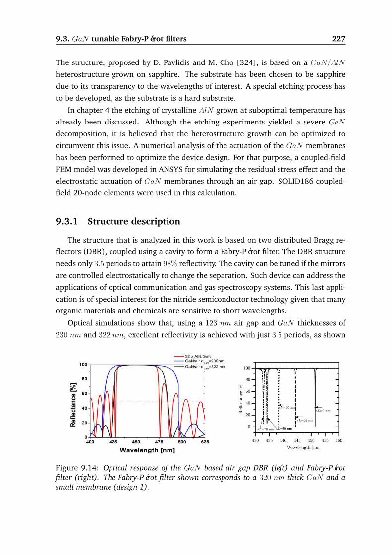
9.3. GaN tunable Fabry-Pérot filters 227
The structure, proposed by D. Pavlidis and M. Cho [324], is based on a GaN/AlN
heterostructure grown on sapphire. The substrate has been chosen to be sapphire
due to its transparency to the wavelengths of interest. A special etching process has
to be developed, as the substrate is a hard substrate.
In chapter 4 the etching of crystalline AlN grown at suboptimal temperature has
already been discussed. Although the etching experiments yielded a severe GaN
decomposition, it is believed that the heterostructure growth can be optimized to
circumvent this issue. A numerical analysis of the actuation of the GaN membranes
has been performed to optimize the device design. For that purpose, a coupled-field
FEM model was developed in ANSYS for simulating the residual stress effect and the
electrostatic actuation of GaN membranes through an air gap. SOLID186 coupled-
field 20-node elements were used in this calculation.
9.3.1 Structure description
The structure that is analyzed in this work is based on two distributed Bragg re-
flectors (DBR), coupled using a cavity to form a Fabry-Pérot filter. The DBR structure
needs only 3.5 periods to attain 98% reflectivity. The cavity can be tuned if the mirrors
are controlled electrostatically to change the separation. Such device can address the
applications of optical communication and gas spectroscopy systems. This last appli-
cation is of special interest for the nitride semiconductor technology given that many
organic materials and chemicals are sensitive to short wavelengths.
Optical simulations show that, using a 123 nm air gap and GaN thicknesses of
230 nm and 322 nm, excellent reflectivity is achieved with just 3.5 periods, as shown
Figure 9.14: Optical response of the GaN based air gap DBR (left) and Fabry-Pérotfilter (right). The Fabry-Pérot filter shown corresponds to a 320 nm thick GaN and asmall membrane (design 1).

228 Chapter 9. MEMS design and simulation
in figure 9.14. With a 322 nm thick GaN layer, a stop band of just 63 nm is achieved,
which is broader than for a 20 period AlN/GaN reflector but needs less layers and
exhibits a larger rejection ratio. The Fabry-Pérot cavity is designed to be centered in
the DBR stop band so a cavity of λ0/2 = 225 nm has been chosen. The actuation
of the mirrors can modify the cavity length; for example, optical simulation shows
that for a displacement of ∆L = 70 nm, the peak wavelength shifts from 450 nm to
431.4 nm. The optical simulations were performed in collaboration with Dr. Cho, and
more information can be consulted in her Ph. D. thesis [324].
For the structure geometry, a square membrane suspended by four beam tethers
has been chosen. The backside of the sapphire is covered with SiO2 for providing
an anti-reflection coating, as shown in figure 9.15. After preliminary analysis, four
designs have been settled to be candidates for the optical device, by varying the
width of membrane and beams, the length of the beams and the thickness of the
GaN layer. These structures were chosen attending to the trade-off between low
deformation and ease of electrostatic actuation and control. The geometry of the
studied structures is listed on table 9.3. In the following sections these structures are
discussed and the effect of residual stress and actuation is presented and analyzed.
Figure 9.15: GaN based air gap DBR and tunable Fabry-Pérot layer and device design.

9.3. GaN tunable Fabry-Pérot filters 229
Design Membrane width Beam width Beam length GaN thicknessDesign 1 20 µm 10 µm 30 µm 230 nmDesign 2 30 µm 15 µm 45 µm 230 nmDesign 1 20 µm 10 µm 30 µm 320 nmDesign 2 30 µm 15 µm 45 µm 320 nm
Table 9.3: Candidate geometries for the Fabry-Pérot filter optimization.
9.3.2 Residual stress effect
The growth of GaN on thick AlN buffers produces a compressive strain that
is rapidly relaxed as the GaN thickness increments. Nonetheless, the strain is not
completely relaxed, and large gradients appear along the heterostructure. For a
GaN/AlN multilayer the situation is more complex: the AlN interlayers tend to
gain their lattice constant and induce a larger strain on the GaN surface grown on
top than the one for the upper GaN surface of the previous layer. As a result, a
stationary strain is never reached, so that large strain gradients are present for all
the layers in the heterostructure. A complete strain relaxation model has been pub-
lished for such heterostructures by Bellet-Amalric et al. [112], a model that we have
used for the calculation of the residual strain and strain gradients along the growth
direction for the heterostructure under study.
The relaxation of the alternatingGaN andAlN layers has been taken into account
for the determination of strain on the top and bottom surfaces of the GaN layers.
The monolayer growth regime strain model was used to analyze the strain on all the
surfaces of the GaN layers for thickness of 230 nm and 320 nm. The bilayer growth
model was also used for calculating the stress on the 320 nm GaN layer. The stress
was calculated from the strain using the data from chapter 7, and the results are
shown on the table 9.4.
GaN surface σ layer 1 σ layer 2 σ layer 3 σ layer 4Low (230 nm, monolayer) 1.654 GPa 1.373 GPa 1.370 GPa 1.366 GPaUp (230 nm, monolayer) 0.595 GPa 0.428 GPa 0.426 GPa 0.425 GPa
Low (320 nm, monolayer) 1.654 GPa 1.367 GPa 1.364 GPa 1.359 GPaUp (320 nm, monolayer) 0.497 GPa 0.341 GPa 0.339 GPa 0.338 GPaLow (320 nm, bilayer) 2.445 GPa 2.061 GPa 2.051 GPa 2.059 GPaUp (320 nm, bilayer) 0.692 GPa 0.514 GPa 0.512 GPa 0.511 GPa
Table 9.4: Absolute value of the compressive residual stress at the GaN surfaces forvarious thicknesses and growth regimes.

230 Chapter 9. MEMS design and simulation
Figure 9.16: Stress distribution in a tether suspended membrane after release (left)and displacement map on the membrane surface (right). In the displacement map aquadrant of the small membrane with 320 nm thick GaN is shown, all the units are inmicrons.
It is observed that the built-in stress gradient [112] in the layers is extremely
large: a value between 2 MPa/nm and 5 MPa/nm is calculated for the layers grown
at monolayer regime. It is also observed that the stress gradient for the last layer in
the stack is about a 10% lower than for the first one. This may pose a detrimental
effect on the device performance as the layer forming the lower and upper mirror
of the Fabry-Pérot filter will have a slightly different stress gradient, and therefore
the parallelism may be compromised after release. Moreover, the layer sequence has
to be adjusted to take into account that the displacement of the two mirrors is not
equal. This can be explained because the bottom mirror is grown on a 113 nm thick
AlN layer that is not completely relaxed, whereas the upper mirror is grown on thick
AlN that can be considered to be fully relaxed.
The calculated stress distribution was used in the FEM model for the determi-
nation of the deformation of the structures induced by the stress relaxation. Large
deformations have been obtained, and a strong dependence on device geometry and
layer thickness has been found. The maximum displacement of the membrane and
the displacement difference in the free-standing membrane have been calculated.
The displacement of the membrane is given by the stress relaxation in the beams,
and the buckling of the membrane is determined by the relaxation of the stress in the
membrane. The buckling in the membrane is large because the residual stress has
been calculated to be complete, as seen in figure 9.16. The structures always buckle
toward the substrate as a result of the compressive stress distribution.
From the simulation results, shown in figure 9.17, it can seen that the design 1
yields to lower displacement but to higher buckling. Additionally, the thicker mem-

9.3. GaN tunable Fabry-Pérot filters 231
Figure 9.17: Displacement (left) and deformation (right) of the GaN membranes afterrelease.
branes exhibit lower displacement and lower buckling. Analyzing the membrane
deformation it is seen that, despite the smaller membrane leads to higher deforma-
tion, the difference with respect to the design 2 is not very large. Thus, taking into
account both displacement and deformation, the optimal design is to use the small
mirror with the thick GaN layer. The optical filter geometry can be further improved
if thicker GaN is used, as the residual strain in the additional thickness will be very
small and both displacement and deformation will be reduced.
In fact, plotting a displacement map on the membrane surface it is observed that,
although the deformation is large, the center of the membrane has little deformation.
This surface map was used in optical simulation [324], and it rendered that a sweet
point diameter between 10 µm and 15 µm could be obtained, which is sufficient for
the intended application. Nonetheless, the AlN spacer layers have to be adjusted in
order to compensate for the deformation of the structure, and thus guarantee that
the whole structure will not collapse on the substrate after release.
9.3.3 Electrostatic actuation
The Fabry-Pérot has been designed to be electrostatically actuated. When a volt-
age difference is applied to the mirrors, an electrostatic force across the air gap
pushes them together. The electrostatic actuation can be controlled up to a third
of the initial gap before the electrostatic force overcomes the elastic restoring reac-
tion. For preventing a short circuit in the structures, the mirrors were oppositely
doped, so in case of collapse a p-n junction will be formed and no current overshoot
will be triggered. The threshold pull-in voltage is given by [325]:

232 Chapter 9. MEMS design and simulation
GaN thickness h0 = 225 nm h0 = 450 nm h0 = 900 nm230 nm 0.784 V | 146 nm 2.635 V | 305 nm 6.207 V | 592 nm320 nm 1.403 V | 151 nm 4.620 V | 304 nm 10.04 V | 590 nm
Table 9.5: Pull-in voltages and gaps for the 20 µm membrane as a function of GaNthickness and initial gap.
Vpull−in =
√8kh30
27ε0A(9.12)
where k is the elastic constant of the membrane structure, h0 the initial gap, and
A the actuator area. A preliminary investigation on the electrostatic actuation, by
solving a prestressed FEM numerical model, revealed that the membranes deviated
from the theoretical behavior. Several factors are responsible for such deviation:
• The structures are small so fringing fields have a considerable influence on the
actuating force.
• The structures are deformed leading to field concentration on the elevated
edges, so the uniform field assumption does not completely hold.
• The actuator is deformed during actuation, modifying its geometry, and there-
fore the electrostatic force has a complex dependence with the gap.
Nevertheless, the deviations are not large and the structures collapse at approx-
imately two thirds of the initial gap. The displacement of the membranes is also
nearly parabolic until collapse, as the theory predicts.
The small membrane design has been analyzed for different initial gaps. The gap
values that were chosen are λ/2 = 225 nm, λ = 450 nm and 2λ = 900 nm in order to
maintain a peak at 450 nm. The results for the pull-in voltage are listed in table 9.5.
It is seen that a limit actuation voltage between 1 and 10 volts is obtained, depending
on the gap and layer thickness. The membrane deformation plot revealed that during
actuation no substantial changes were induced with respect to those obtained for the
residual strain relaxation analysis. As can be observed in table 9.5, the objective of
controlling ∆h = 70 nm is possible for both thicknesses, although the value is close to
the pull-in voltage and control at this deviation is difficult as a noise of few millivolts
can drive the structure into collapse.

9.4. Conclusions 233
9.4 Conclusions
In this chapter, both the technology optimized in this thesis and the data obtained
for the microstructure characterization, were applied to several cases of application
in order to obtain optimized devices. Two AlN/NCD piezoelectrically actuated de-
vices have been studied and a GaN based optical MEMS structure was simulated.
For the AlN/NCD system the following conclusions can be extracted:
• The Young’s modulus of both materials, AlN and NCD, yield to the existence
of an optimal AlN thickness for maximizing the displacement at a fixed field
across the piezoelectric layer. The acuteness of the optimum thickness curve
varies depending on the symmetry of the structure, but for all cases the optimal
AlN thickness was found to be 78−80% of the NCD thickness. On the contrary,
for sensing transducers, the AlN thickness shall be reduced as much as the
piezoelectric response allows.
• The frequency drop caused by the addition of the AlN layer to NCD resonant
structures has been calculated to be moderate, the frequency is multiplied by a
0.75 factor for beams covered by an optimal AlN transducer thickness.
• The AlN transducer optimal length has been calculated for three different
structures:
– Single clamped cantilever: The optimal length of the transducer is the
total cantilever length.
– Double clamped beams with a transducer on each clamping working un-
der symmetric polarization: For this structure the optimal length of each
transducer is to span a length 30% of the total beam length.
– Circular membrane with annular transducer on the outer part of the mem-
brane: For this structure the radius of the transducer is optimized at a 40%
of the membrane radius.
• The influence of the electrodes can be neglected if the NCD is doped to act as
lower electrode, and a metal with thickness below 30 nm is used as the other
electrode. The resonance frequency is virtually not affected if Cr is used. The
displacement has to be corrected by a factor below 10% in the case of Ti, having
no impact on the optimal electrode thickness and length.

234 Chapter 9. MEMS design and simulation
Coupled cantileverAlN/NCD-based structures were designed to act as high power
field emission switches. Both vertical and lateral actuation was explored, providing
design rules as a function of bimorph thickness and cantilever dimensions. Resonance
frequencies in the range of 10 MHz are attainable using this device. Conversely, the
AlN/NCD membranes were applied to the design of tunable microlenses, showing
that large actuation range may be designed. In particular, large area spherical lenses
with diameters longer than one millimeter, can be controlled to provide a curvature
radius Rcur ∈ [27.7 mm,∞].
Regarding the single crystal, nitride-based MEMS, a membrane based structure
has been analyzed. A numerical model was developed for studying the deformation
and displacement of the structure under residual strain relaxation and electrostatic
actuation. The structure was designed to be two 3.5 period Bragg reflectors separated
by an air cavity, forming a Fabry-Pérot filter. The residual strain distribution was
calculated using the Bellet-Amalric relaxation model [112] for the alternative AlN
sacrificial layers and GaN functional layers.
The deformation of the structures is large, due to the high residual compressive
stress gradient. However, the simulation results show that the 20 µm square mem-
branes have a diameter between 10 µm and 15 µm at the center that can be used
for the optical application, depending on the aberration requirements on the mirror.
Though the displacement of the structure is in the micron range, but is consistent
among layers, so it can be easily compensated adjusting the AlN spacer layer.
Finally, the electrostatic actuation was also simulated for the pre-stressed mem-
branes. Limit actuation voltages from 1 to 10 volts were calculated, depending on
the GaN layer thickness and the initial cavity length (λ/2, λ or 2λ). No significant
additional deformation of the membrane was found to be produced during the actu-
ation, and a gap reduction down to 2h0/3, before structure collapse, was obtained.
Therefore, the 225 nm cavity can be tuned down to 150 nm; it should be taken into
account that severe noise restrictions are required for a reduction beyond 170 nm, in
order to avoid accidental structure collapse.
On the whole, complex MEMS structures were simulated for the various material
systems of interest in this thesis. Detailed models were developed including the
gathered material parameters and the observed fabrication imperfections in order to
provide accurate predictions on the behavior of the studied devices.

Part IV
Conclusions and Future Work
235


Chapter 10
General conclusions
In this thesis a large amount of work on several aspects of NCD and III-N tech-
nological processing steps has been presented. The MEMS fabrication techniques
for the materials of interest has been studied and optimized, leading to several new
observations that were either published in peer-reviewed journals or presented in
international conferences. The fabricated devices were measured and a complete
mechanical characterization has been provided and published in scientific journals,
for a publication list originated by this thesis refer to appendix B. Models for the pre-
diction of the device performance were developed and the obtained results are con-
sistent with other publications that were released after the conclusion of this work.
Finally, the models were used for the design of complex devices in order to find op-
timized device topologies, that have been reused in later research by collaborating
groups. In what follows, a brief summary of the most important results reported in
this thesis is given, as well as some closing remarks on the relevance of the work pre-
sented in this dissertation. For a more detailed summary on a specific topic covered
by this thesis please refer to the conclusions of the corresponding chapter.
Regarding the fabrication techniques optimization, the following processes have
been studied:
• Dry etching for functional layer patterning
• Dry and wet etching of sacrificial layers
• Determination of the properties of the polycristalline AlN adaptation layer that
is deposited near the substrate interface using reactive sputtering, including the
exploration of the boundary conditions that give rise to the formation of this
layer
• Etching procedures for nanometric pore induction on GaN surface
237

238 Chapter 10. General conclusions
The dry anisotropic etching of III-N materials for pattern transfer was studied
using RIE with SiCl4 : Ar : SF6 plasmas and the general observations that have been
made are:
• The addition of SF6 increases the etching speed of GaN as well as produces
a polishing effect that reduces the surface roughness and the sidewall slope.
These effects have been explained by the formation of easier to etch NF3 at the
N-planes of the semiconductor.
• For AlN , the SF6 also increases etching speed but high selectivity to GaN can
be achieved. However, the surface native oxide shows a very high resistance
to the etching process, severely decreasing the etch rate at the first nanometers
of the material. This effect of the native oxide has been found to be defect
dependent. In fact, for AlN grown on Si(111) the etch rate drop is lower than
for other substrates. This effect of the native oxide was not observed for the
other III-N materials.
• For InN , the addition of SF6 may lead to residues accumulation on the surface,
attributed to low volatile InF3 droplets. The measured etching speed is similar
to that calculated for GaN .
• For Al0.17In0.83N lattice-matched to GaN layers the behavior is very similar to
the observed for the AlN films but with an easier to etch native oxide. High se-
lectivity with respect to GaN can be obtained adjusting the process parameters
and the SF6 proportion.
This optimization and characterization of the III-N patterning has been published
in a journal paper [326] and presented in international conferences [327,328].
Nanocrystalline diamond anisotropic patterning was also studied using H2 : O2
plasma reactive ion etching. The high power used for the NCD etching leads to the
fact that the use of hard metal masks is required to withstand the process, otherwise
the mask is etched away. The etch rates obtained are low, although the use Ni masks
allow to achieve etching with steep sidewalls regardless of the methane concentration
used during the growth.
Besides, the other etching processes required for the fabrication of MEMS, the
isotropic sacrificial etching, have been studied, and various sacrificial layers have
been proposed. Three approaches have been explored:
• The fabrication of good quality NCD on Si(001) and III-N devices on Si(111) has
been performed by optimizing HNA wet etching and dry reactive ion etching in

239
SF6 plasmas. The dry process has been found to be cleaner, compatible with
oxides and metallizations and easier to control. Indeed, the wet etching process
has yielded very large etching rates, which makes this procedure more suitable
for bulk rather than surface micromachining.
• AlInN lattice matched to GaN was used to produce GaN free-standing struc-
ture. High selectivity with respect to GaN using KOH wet chemical etches was
achieved and the etching process was studied to find that it is defect driven. The
results of this study have been published in a journal paper [127] and presented
in international conferences [329,330].
• Single crystal AlN grown by MOCVD at suboptimal temperature (850C). The
etching of such material has been done in KOH solutions with high speeds.
The production of GaN free-standing structures is hampered by the difficulty
of high quality layer growth over the substrate.
Having completed the optimization of the etching processes required for the fab-
rication of the free-standing structures, the functional layers have been studied, with
the following conclusions:
• For driving NCD MEMS with piezoelectric AlN actuators the sputtering deposi-
tion of thin (d < 200 nm) polycristalline AlN films with a preferred orientation
is required for the actuation of the purposed devices. In this work, the bound-
aries for the production of such thin layers with piezoelectric response have
been mapped using silicon as a substrate. It has been determined that an amor-
phous adaptation layer is formed on the substrate, which is highly responsible
for the charge trapping in the material and the lowering of the electric break-
down field. The formation of this adaptation layer is minimized at low pressure
and high power. The crystal quality of the material is enhanced if the target to
substrate distance is reduced, although the formation of a thin adaptation layer
was also observed for low dts. Nevertheless, piezoresponse has been measured
for AlN films with d = 120 nm. It is worth extending this mapping substrate
temperatures above room temperature, as it is believed that the film quality
will be enhanced and the adaptation layer suppressed.
• The formation of pores on the GaN surface has been observed for etches using
HF : H2O2 chemistry. The process has been found to require high HF concen-
trations and high UV illumination power due to the stability of GaN . For this

240 Chapter 10. General conclusions
aggressive process, a formation of pores with 50 nm diameter and a concentra-
tion of 109− 1010 cm−2 have been measured. This layer is fully relaxed and can
act as a sacrificial layer for the growth of relaxed GaN . Moreover, the porous
GaN has been found to be etched at higher speeds than GaN and can be,
therefore, used as a sacrificial layer for MEMS device technology. Additionally,
the porous surface has been found to yield to an enhanced functionalization
efficiency of the GaN , and thus it can be used for the fabrication of high sen-
sitivity gas and chemical sensors. This work was presented in an international
conference [331].
After the optimization of the fabrication processes, free-standing structures have
been produced for material and device characterization. The results obtained for the
two material systems of interest for this dissertation are the following:
• III-N materials, grown by MBE on Si(111), have been characterized in order
to extract the main materials parameters. The determination of the Young’s
modulus of the binary materials has been done using the AFM beam bend-
ing technique. The values obtained are close to the theory and to the values
obtained by other techniques on clamped films. Regarding the large residual
strain, it has been found to be fully relaxed for AlN and InN , although a thin
layer at the interface with the substrate had a residual strain that produced
a moderate buckling toward the substrate after the structures were released.
Conversely, GaN retained a large residual strain, and the release process in-
duced an uneven relaxation that severely deformed the structures with asym-
metric clamping. Moreover, the underetch at the clampings induced a slope on
the cantilever-like devices due to the uneven strain relaxation. The complete
study was presented in international conferences [332,333] and published in a
journal [334].
• NCD free-standing structures were also fabricated for static and dynamic char-
acterization. The combined analysis provided a large Young’s modulus (E ≥950 GPa) that is increased if the methane concentration is reduced during ma-
terial growth. Nevertheless, the material deposited with low methane con-
centration exhibited a large tensile residual strain. The high stiffness of the
material makes that the non-linear vibrational behavior of the structures is
dominated by geometrical parameters rather than by inertia effects, and can
be modeled using the Duffing model. A model for the resonance frequency de-
termination has been derived to include fabrication imperfections and residual

241
stress. The resonance frequency can be further improved if the metal thickness
and the w/d ratio are reduced. In fact, the metal layer hindered the achieve-
ment of highQ values, dominating the damping of the long resonators and even
hampering the measurement of the molecular damping when the pressure is in-
creased. This characterization has been published in a journal paper [335] and
presented in an international conference [336].
Finally, the models and data presented in this thesis have been applied to the
study of AlN/NCD piezoelectrically actuated devices and to GaN membranes with
electrostatic actuation.
• For AlN/NCD devices, a polycristalline AlN actuator deposited by sputtering
over an NCD elastic carrier has been considered. The optimal thickness of the
AlN actuator layer has been found to be in the range of 0.78− 0.82 of the NCD
thickness, depending on the metallization used for the upper electrode. Despite
that if the metal thickness increases the AlN proportion has to be also increased
to maintain the actuator optimality, if the metal is thin (d ≈ 30 nm) the effect
on the optimal AlN thickness may be neglected. Conversely, the resonance fre-
quency is very slightly reduced if the thin metal is considered (5% drop for Cr
electrode and 10% for Ti,) so that the metal can be left out from the modeling
and the obtained data corrected at a second step. Optimized electrode topolo-
gies have been calculated for AlN/NCD beams and circular membranes, and
have been used to model high power, beam based, microswitches and tunable
lenses using circular AlN/NCD membranes. These results and models have
been used for later research at the Fraunhofer IAF [322].
• GaN membranes have been modeled for tunable Fabry-Pérot filter applications.
The strain relaxation has been modeled and the optimized design was demon-
strated to be compatible with optical requirements. The electrostatic actuation
of the structure was also modeled and actuation voltages and thresholds have
been determined for various geometries. This work was presented in an inter-
national conference [337] and published in a journal paper [338].
On the whole, a complete device development is presented in this dissertation,
spanning from fabrication process optimization to device design, going through ma-
terial and device characterization. A wide range of techniques have been used to
provide a full characterization that has led to complete models that can be used for
the design of NCD and III-N MEMS devices for various applications in harsh environ-
ments.


Chapter 11
Future work
The extension of the work presented in this volume has opened a lot of possible
research activities that can be followed. The variety of the topics addressed in this
thesis makes impossible pursuing some of the opened ways either in fabrication of
structures, characterization of their properties, or application in MEMS devices. The
most relevant topics that can be further researched to improve or continue with the
work presented in this dissertation are listed in this last chapter.
Regarding the fabrication techniques:
• Epitaxial growth optimization of GaN/LT−AlN and GaN/AlInN heterostruc-
tures. The challenge of the all nitride etching processing technology mainly lies
on the difficulty of growing high-quality material on a suitable sacrificial layer.
A growth condition research has to be undertaken in order to improve the re-
sults obtained in this work.
• Deposition of polycristalline AlN by sputtering at high temperature (tempera-
tures up to 400C) for producing thin layers with high piezoelectric response.
Once the boundaries for adaptation layer reduction have been identified, the
adatoms can be further energized by heating the substrate. The increase of
the temperature would lead to very high quality AlN layers with piezoelectric
response for d < 200 nm.
• Epitaxial growth of GaN on porous substrates. The nP − GaN layers can be
used as a special sacrificial substrate , but the regrowth of continuous GaN
layers on top has to be optimized.
Regarding the material properties characterization:
243

244 Chapter 11. Future work
• Determination of electric properties o nitride suspended structures. The inte-
gration of electrodes on III-N free-standing structures is required for measuring
how the mechanization affects the electrical properties. The measurement of
lateral depletion lengths, carrier concentration, and mobility of the suspended
materials and HEMT heterostructures is required for adjusting the design of
advanced sensors. Moreover, the absence of parallel conduction paths would
provide accurate characterization of the intrinsic properties of the materials.
• Measurement of the electrical and mechanical properties of doped NCD. This
material can act as elastic carrier and electrode, so that the properties of this
material have to be determined in order to modify the device models.
• Measurement of field emission from free-standing NCD tips. The field emis-
sion across nanogaps has to be measured in order to validate the design of the
switch concept. Other factors that could hinder this device performance, such
as electrostatic restoration force, have also to be characterized.
Regarding the MEMS devices:
• Integration of polycristalline AlN on NCD for static and dynamic actuation.
The transduction properties of the bimorph have to be verified using static and
resonant devices.
• Functionalization of nP−GaN surfaces for high sensitivity biological and chem-
ical sensors. Additionally, the fabrication of diodes with semitransparent con-
tacts on nP −GaN layers can also be used for enhancing the sensitivity of gas
sensors working in harsh environments.
• Fabrication of membranes of GaN on LT − AlN for validating the modeling
and characterization the electrostatic actuation of the structures.

Part V
Appendixes
245


Appendix A
Analytic model for the resonancemodes of beams
In this appendix analytic equations for the resonance frequencies and mode shapes
of single and double clamped beams are derived following [339, 340]. The Euler-
Bernoulli frame work will be followed. Thus the following assumptions shall be
verified:
1. The cross-section is infinitely rigid in its own plane.
2. The cross-section of a beam remains plane after deformation.
3. The cross-section remains normal to the deformed axis of the beam.
This assumptions are easily verified by the structures used in this dissertation as
the thickness of the beams is small, thus the normal planes to the neutral axis remain
normal after deformation. Under these assumptions the Euler-Bernoulli model for
static displacement of a homogeneous beam (of length L, width w and thickness d)
under an uniform load is [339]:
∂2
∂x2
(EI
∂2u
∂x2
)= q (A.1)
where u is the displacement along z axis, E is the Young’s modulus, I the moment
of inertia (given by I = wd3
12for a rectangular beam) and q the distributed load (force
per unit length).
The boundary conditions for a cantilever, or single clamped beam are given by
u|x=0 =∂u
∂x
∣∣∣∣x=0
=∂2u
∂x2
∣∣∣∣x=L
=∂3u
∂x3
∣∣∣∣x=L
= 0 (A.2)
247

248 Chapter A. Analytic model for the resonance modes of beams
which applied to (A.1) provide the deformation function for a cantilever:
ucantilever(x) =q
24EI
[x4 − 4Lx3 + 6L2x2
]0 ≤ x ≤ L (A.3)
Conversely, the boundary conditions for a double clamped beam are
u|x=0 =∂u
∂x
∣∣∣∣x=0
= u|x=L =∂u
∂x
∣∣∣∣x=L
= 0 (A.4)
which applied to (A.1) provide the deformation function for a double clamped
beam:
ubeam(x) =q
24EI
[x4 − 2Lx3 + L2x2
]0 ≤ x ≤ L (A.5)
The dynamic beam equation is formed from the energy balance equation:
S =
∫ L
0
[ρdw
2
(∂u
∂t
)2
− EI
2
(∂2u
∂x2
)2
+ qu(x, t)
](A.6)
where ρ is the density of the material. In A.6 the first term represents the ki-
netic energy, the second the potential energy due to internal restoration forces and
the third term represents the potential energy due to the external load. For and
Euler-Bernoulli beam the function that minimizes the functional S, Euler-Lagrange
equation, is given by
∂2
∂x2
(EI
∂2u
∂x2
)= −ρdw∂
2u
∂t2+ q(x) (A.7)
For the free vibration case (q = 0) the equation (A.7) may be solved by Fourier
decomposition into the sum of harmonic vibrations of the general form
un = A1 cosh (βnx) + A2 sinh (βnx) + A3 cos (βnx) + A4 sin (βnx) (A.8)
where βn depends on the modes natural angular frequencies ωn (ω = 2πf):
βn =4
√ρdwω2
EI(A.9)
The existence of a natural resonance mode for cantilever requires that the fre-
quency satisfies:
cosh (βnL) cos (βnL) + 1 = 0 (A.10)
For doubled clamped beams the natural frequencies are given by

249
cosh (βnL) cos (βnL)− 1 = 0 (A.11)
The normalized mode shape for a cantilever beam is calculated using (A.2) in
(A.8):
un = cosh (βnx)− cos (βnx) +[cosh (βnx) + cos (βnx)] [sin (βnx)− sinh (βnx)]
sin (βnx) + sinh (βnx)(A.12)
For a double clamped beam an approximation can be followed. In the case of
forced vibrations induced by an uniform load, the mode shape of the fundamen-
tal mode can be approximated using (A.5). Using this displacement in the balance
equation (A.6), the fundamental frequency is given by
f01 =3√
14
2π√
3
√E
ρ
d
L2(A.13)
which provides a good approximation of the exact analytical solution.


Appendix B
Publications
This appendix lists the publications and contribution to conferences that the work
described in this volume has produced.
B.1 Paper published in peer reviewed journals
• E. Sillero, F. Calle, M. A. Sánchez-García. “GaN reactive ion etching usingSiCl4 : Ar : SF6 chemistry”. Journal of Material Science: Materials in Elec-
tronics 16 (2005) 409.
• E. Cho, D. Pavlidis, E. Sillero. “GaN/air gap based micro-opto-electro-mechanical(MOEM) Fabry-Pérot filters”. Physica Status Solidi (c) 4 (2007) 2764.
• E. Sillero, D. López-Romero, F. Calle, M. Eickhoff, J. F. Carlin, N. Grandjean,
M. Illegems. “Selective etching of AlInN/GaN heterostructures for MEMS tech-nology”. Microelectronic Engineering 84 (2007) 1152.
• E. Sillero, D. López-Romero, A. Bengoechea, M. A. Sánchez-García, F. Calle.
“Fabrication and stress relief modelling of GaN based MEMS test structures grownby MBE on Si(111)”. Physica Status Solidi (c) 5 (2008) 1974.
• R. Cuerdo, E. Sillero, M. F. Romero, M. J. Uren, M-A. di Forte Poisson, E.
Muñoz, F. Calle. “High-Temperature microwave performance of submicronAlGaN/GaN HEMTs on SiC”. IEEE Electron Decive Letters 30 (2009) 808.
• E. Sillero, O. A. Williams, V. Lebedev, V. Cimalla, C-C. Röhlig, C. E. Nebel,
F. Calle. “Static and dynamic determination of the mechanical properties ofnanocrystalline diamond micromachined structures”. Journal of Micromechan-
ics and Microengineering 19 (2009) 115016.
251

252 Chapter B. Publications
• W. Smirnov, A. Kriele, R. Hoffmann, E. Sillero, J. Hees, O. A. Williams, N. Yang,
C. Kranz, C. E. Nebel. “Diamond-Modified AFM probes: From diamond nanowiresto atomic force microscopy-integrated boron-doped diamond electrodes”. Analyti-
cal Chemistry 83 (2011) 4936.
B.2 Contributions to conferences
• E. Sillero, F. Calle, M. A. Sánchez-García. “Plasma processing for GaN basedtechnology”. 13th European Workshop on Heterostructure Technology (2004).
• E. Sillero, F. Calle, M. A. Sánchez-García. “GaN reactive ion etching usingSiCl4 : Ar : SF6 chemistry”. 5th International Conference on Materials for
Microeletronics and Nanoengineering (2004).
• J. Pedrós, R. Cuerdo, J. Grajal, E. Sillero, Z. Bougrioua, F. Calle. “Gate-biasedSAW devices on AlGaN/GaN heterostructures”. 14th European Workshop on
Heterostructure Technology (2005).
• E. Sillero, F. Calle, M. Eickhoff, J. F. Carlin. “Etching procedures for III-Nmicrosystems technology”. 7th International Conference on Materials for Mi-
croeletronics and Nanoengineering (2006).
• E. Sillero, F. Calle, D. López-Romero, M. Eickhoff, J. F. Carlin, N. Grandjean,
M. Ilegems. “Selective etching of AlInN/GaN heterostructures for MEMS tech-nology”. 32nd Conference on Micro- and Nano- Engineering (2006).
• E.Cho, E. Sillero, D. Pavlidis, G. Zhao, S. Seo, S. Jatta, B. Kögel, P. Meissner.
“GaN/Air gap based Micro Opto Electro Mechanical Fabry-Pérot Filters”. 4th In-
ternational Workshop on Nitride Semiconductors (2006).
• E. Sillero, A. Bengoechea, M. A. Sánchez-García, F. Calle. “III-Nitride MEMSgrown by MBE on Si(111): Fabrication and mechanical characterisation”. 16th
European Workshop on Heterostructure Technology (2007).
• E. Sillero, D. López-Romero, A. Bengoechea, M. A. Sánchez-García, F. Calle.
“Fabrication and stress relief modelling of GaN based MEMS test structures grownby MBE on Si(111)”. 7th International Conference on Nitride Semiconductors
(2007).

B.2. Contributions to conferences 253
• E. Sillero, M. Eickhoff, F. Calle. “Nanoporous GaN by UV assited electrolessetching for sensor applications”. 5th International Workshop on Nitride Semi-
conductors (2008).
• R. Cuerdo, E. Sillero, M. F. Romero, M. Uren, E. Muñoz, F. Calle. “DC and RFperformance of AlGaN/GaN HEMTs on SiC at high temperatures”. 5th Interna-
tional Workshop on Nitride Semiconductors (2008).
• E. Sillero, J. Pedrós, R. San Román, G. F. Iriarte, F. Calle. “RF MEMS switcheswith III-N technology”. 32nd Workshop on Compound Semiconductors and Inte-
grated Circuits (2008).
• E. Sillero, O. A. Williams, V. Lebedev, V. Cimalla, C. C. Röhlig, C. E. Nebel, F.
Calle. “Nanocrystalline diamond microelectromechanical resonators”. 33rd Work-
shop on Compound Semiconductors and Integrated Circuits (2009).
• G. F. Iriarte, E. Sillero, J. G. Rodríguez, A. Navarro, J. Pedrós, F. Calle. “E-beam lithography of nano interdigital transducers on insulating, semiconductingand conductive substrates”. 33rd Workshop on Compound Semiconductors and
Integrated Circuits (2009).
• F. Knöbber, E. Sillero, C-C. Röhlig, O. A. Williams, R. E. Sah, L. Kriste, V.
Cimalla, C. E. Nebel, F. Calle, V. Lebedev. “Piezoelectrically actuated AlN andnanodiamond microstructures”. 18th European Workshop on Heterostructure
Technology (2009).


Appendix C
Glossary
This appendix lists the acronims and most common symbols, with SI units, used
in this volume.
C.1 Acronyms
Acronym Definition
2DEG Two Dimensional Electron Gas
AFM Atomic Force Microscope (Microscopy)
C-f Capacitance-Frequency (curve)
C-V Capacitance-Voltage (curve)
CCD Charge-Coupled Device
CPW CoPlanar Waveguide
CSIC Consejo Superior de Investigaciones Científicas
CVD Chemical Vapor Deposition
DBR Distributed Bragg Reflector
DC Direct Current
DLC Diamond Like Carbon
eBeam Electron Beam
EPFL École Polytechnique Fédérale de Lausanne
FBAR Thin-Film Bulk Acoustic Resonator
FEA Finite Element Analysis
FEM Finite Element Method
FTIR Fourier Transform InfraRed (spectroscopy)
FWHM Full Width at Half Maximum
255

256 Chapter C. Glossary
GSG Ground-Signal-Ground
HEMT High Electron Mobility Transistor
HNA Hydrofluoric, Nitric, Acetic acid (HF − HNO3 −CH3COOH)
HRXRD High Resolution X-Ray Diffraction (Diffractometry)
I-V Current-Voltage (curve)
IAF Fraunhofer Institute für Angewandte Festkörperphysik
IC Integrated Circuit
ICCM Instituto de Ciencias de Materiales de Madrid
ICP Inducted Coupled Plasma (reactor)
III-N Group III Nitride semiconductors
ISOM Instituto de Sistemas Optoelectrónicos y Microtecnología
LED Light Emitting Diode
LT-AlN Low Temperature grown Alluminum Nitride
MBE Molecular Beam Epitaxy
MEMS Micro-Electro-Mechanical Systems
MIM Metal Insulator Metal structure
MIS Metal Insulator Semiconductor structure
MOCVD Metal-Organic Chemical Vapor Deposition
MOEMS Micro-Opto-Electro-Mechanical Systems
MOVPE Metal-Organic Vapor Phase Epitaxy
NCD NanoCrystalline Diamond
NEMS Nano-Electro-Mechanical Systems
nP-GaN NanoPorous Gallium Nitride
PEC Photo-Electro-Chemical (reaction/etching)
PECVD Plasma Enhanced Chemical Vapor Deposition
PL Photo-Luminescence
PMMA PolyMethyl Methacrylate
PZT Lead zirconate titanate
RF Radio Frequency
RIE Reactive Ion Etching
RMS Root Mean Square
RTA Rapid Thermal Annealing
SAW Surface Acoustic Wave
SEM Scanning Electron Microscope (Microscopy)

C.2. Symbols 257
SI International System of units
TMHA Tetra-Methyl-Ammonium Hydroxide
TUD Technische Universität Darmstadt
UNCD UltraNanoCrystalline Diamond
UPM Universidad Politécnica de Madrid
UV UltraViolet
WLI White Light Interferometer (Interferometry)
VLSI Very Large Scale of Integration
C.2 Symbols
Symbol Definition
A Area [m2]
B Magnetic field [T ]
cij Elastic coefficient[Nm2
]Cfb Flat band capacitance [F ]
d Layer thickness [m]
dij Piezoelectric coefficient[CN
]dts Target-substrate distance [m]
δu Underetch distance correction factor [adim]
eij Converse piezoelectric coefficient[NC
]E Young’s modulus [Pa]
E Energy [J ]
ε Strain [adim]
ε Infinitesimal [adim]
f Frequency [Hz]
γ Piezoelectric coverage ratio [adim]
γn Stress correction factor [adim]
I Inertia moment [m4]
k Spring constant[Nm
]L Beam length [m]
LD Debye length [m]
λ Wavelength [m]
m Mass [Kg]
NF Charge density [m−3]

258 Chapter C. Glossary
ν Poisson ratio [adim]
p Pressure [Pa]
PRF Radiofrequency power [W ]
φ Mass flux [sccm]
Q Quality factor [adim]
ρ Mass density[Kgm3
]sij Elastic compliance coefficient
[m2
N
]σ Stress [Pa]
t Time [s]
T Temperature [C]
θ Angle []
u Normalized mode shape [adim]
V Voltage [V ]
VDC Plasma autopolarization voltage [V ]
Vfb Flat band voltage [V ]
w Beam width [m]
W Beam separation in U-shaped resonators [m]
zmm Neutral axis position [m]

References
[1] Feynman, R. P., There’s plenty of room at the bottom, in American PhysicalSociety Meeting, Pasadena, CA, 1959.
[2] Nathanson, H. C. and Wickstrom, R. A., IEEE Transactions on Electronic De-vices ED12 (1965) 507.
[3] Roylance, R. M. and Angell, J. B., IEEE Transactions on Electronic Devices 26(1979) 1911.
[4] Binnig, G., Rohrer, H., Gerber, C., and Weibel, E., Physical Review Letters 49(1982) 57.
[5] Binnig, G., Quate, C. F., and Gerber, C., Physical Review Letters 56 (1986)930.
[6] Iijima, S., Nature 354 (1991) 56.
[7] Thess, A. et al., Science 273 (1996) 483.
[8] Yole Dévelopment reports, Status of the MEMS Industry, Yole Développement,May 2015.
[9] Wright, N., Horsfall, A. B., and Vassilevski, K., Materials Today 11 (2008) 16.
[10] Willander, M., Friesel, M., Wahab, Q. U., and Strumal, B., Journal of MaterialsScience: Materials in Electronics 17 (2006) 1.
[11] Joshi, R. K. and Kumar, A., Journal of Nanomaterials 2009 (2009) 637530.
[12] Butler, J. E. et al., Journal of Nanomaterials 2009 (2009) 637530.
[13] Kohn, E. et al., Physics D: Applied Physics 34 (2001) R77.
[14] Cimalla, V., Petzoldt, J., and Ambacher, O., Physics D: Applied Physics 40(2007) 6386.
[15] Saadon, S. and Sidek, O., Energy Conversion and Management 52 (2011)500.
[16] Faucher, M. et al., Applied Physical Letters 94 (2009) 233506.
259

260 REFERENCES
[17] Popa, L. C. and Weinstein, D., Switchable piezoelectric transduction in Al-GaN/GaN MEMS resonators, in Proceeding of the Transducers InternationalConference, page 2461, 2013.
[18] Ansari, A. and Rais-Zadeh, M., An 8.7 GHz GaN micromechanical resonatorwith an integrated AlGaN/GaN HEMT, in Proceedings of the Solid-State Sen-sors, Actuators and Microsystems Workshop, volume 812, page 295296, 2014.
[19] Gil, B., Group III Nitride Semiconductor Compounds, Number 6 in Series onsemiconductor science and technology, Clarendon press, 1998.
[20] Madelung, O., Semiconductors: Data Handbook, Springer, 2004.
[21] Levinshtein, M. E., Rumyantsev, S. L., and Shur, M. S., Properties of AdvancedSemiconductor Materials: GaN, AlN, InN, BN, and SiGe, John Wiley and Sons,2001.
[22] Matsuoka, T., Okamoto, H., Nakao, M., Harima, H., and Kurimoto, E., AppliedPhysical Letters 81 (2002) 1246.
[23] Grandal, J., Sánchez-García, M. A., Calle, F., and Calleja, E., Physica StatusSolidi C 2 (2005) 2289.
[24] Nakamura, S. and Krames, M. R., Proceedings of the IEEE 101 (2013) 2211.
[25] Porowski, S., Journal of Crystal Growth 189 (1998) 153.
[26] Grzegory, I., Journal of Physics: Condensed Matter 13 (2001) 6875.
[27] Akasaki, I., Kito, H. A. M., and Hiramatsu, K., Journal of Crystal Growth 98(1989) 209.
[28] Semond, F. et al., Physica Status Solidi A 188 (2001) 501.
[29] Calleja, E. et al., Journal of Applied Physics 82 (1997) 4681.
[30] Popovici, G., Morkoç, H., and Mohammad, S., Group III Nitride SemiconductorCompounds, Number 6 in Series on semiconductor science and technology,Clarendon press, 1998.
[31] Sánchez-García, M. A., Crecimiento y caracterización de nitruros del grupoIII sobre Si (111) por epitaxia de haces moleculares, PhD thesis, E. T. S. I.Telecomunicación, Universidad Politécnica de Madrid, 2000.
[32] Mohammad, S., Salvador, A. A., and Morkoç, H., Emerging gallium nitridebased devices, in IEEE Proceedings, volume 83, page 1306, 1995.
[33] H., Cingolani, R., and Gil, B., Solid-State Electronics 43 (1999) 1909.
[34] Pearton, S. J., Ren, F., Zhang, A., and Lee, K. P., Material Science and Engi-neering R30 (2000) 55.

REFERENCES 261
[35] Williams, O. A., Diamond and Related Materials 20 (2011) 621.
[36] Achatz, P. et al., Physical Review B 74 (2006) 155429.
[37] Gajewski, W. et al., Physical Review B 79 (2009) 45206.
[38] Williams, O. A. et al., Chemical Physics Letters 445 (2007) 255.
[39] Williams, O. A. et al., Diamond and Related Materials 17 (2008) 1080.
[40] Gruen, D. M., Material Research Society Bulletin 26 (2001) 772.
[41] Williams, O. A. et al., Diamond and Related Materials 15 (2006) 654.
[42] Ohtsuka, K., Suzuki, K., Sawabe, A., and Inuzuka, T., Japanese Journal ofApplied Physics part 2 - Letters 35 (1996) L1072.
[43] Butler, J. E., Mankelevich, Y. A., Cheesman, A., Ma, J., and Ashfold, M. N. R.,Journal of Physics - Condensed Matter 21 (2009) 364201.
[44] Angadi, M. A. et al., Journal of Applied Physics 99 (2006) 114301.
[45] Williams, O. A. et al., Chemical Physics Letters 495 (2010) 84.
[46] Kriele, A. et al., Applied Physical Letters 95 (2009) 031905.
[47] Imboden, M. and Mohanty, P., Physical Review B 79 (2009) 125424.
[48] Tadjer, M. J. et al., Applied Physical Letters 91 (2007) 163508.
[49] Zimmermann, T. et al., Diamond and Related Materials 14 (2005) 416.
[50] Rabarot, M. et al., Diamond and Related Materials 19 (2010) 796.
[51] Raleva, K., Vasileska, D., and Goodnick, S. M., IEEE Electron Device Letters29 (2008) 621.
[52] Erdemir, A. et al., Surface and Coatings Technology 121 (1999) 565.
[53] Sekaric, L. et al., Applied Physical Letters 81 (2002) 4455.
[54] Gaidarzhy, A., Imboden, M., Mohanty, P., Rankin, J., and Sheldon, B. W.,Applied Physical Letters 91 (2007) 203503.
[55] Imboden, M., Mohanty, P., Gaidarzhy, A., Rankin, J., and Sheldon, B. W.,Applied Physical Letters 90 (2007) 173502.
[56] Hutchinson, A. B. et al., Applied Physical Letters 84 (2004) 972.
[57] Krauss, A. R. et al., Diamond and Related Materials 10 (2001) 1952.
[58] Guillén, F. J. H., Janischowsky, K., Kusterer, J., Ebert, W., and Kohn, E., Dia-mond and Related Materials 14 (2005) 411.

262 REFERENCES
[59] Mandal, S. et al., Nanotechnology 21 (2010) 195303.
[60] Huff, M. A., Aidala, D. A., and Butler, J. E., Solid State and Technology 49(2006) 45.
[61] Kohn, E., Gluche, P., and Adamschik, M., Diamond and Related Materials 8(1999) 934.
[62] Kohn, E., Adamschik, M., Schimd, P., Ertl, S., and Floter, A., Diamond andRelated Materials 10 (2001) 1684.
[63] Wang, J., Butler, J. E., Feygelson, T., and Nguyen, C. T. C., 1.51 GHz nanocrys-talline diamond micromechanical disk resonator with material-mismatchedisolating support, in IEEE International Conference on Micro Electro MechanicalSystems, volume 17, page 641, 2004.
[64] Srinivasan, S., Hiller, J., Kabius, B., and Auciello, O., Applied Physical Letters90 (2007) 134101.
[65] Hikavyy, A., Clauws, P., VAnbesien, K., Visschere, P. D., and Williams, O. A.,Diamond and Related Materials 16 (2007) 983.
[66] Benedic, F. et al., Diamond and Related Materials 17 (2008) 804.
[67] Martin, H. B., Argoitia, A., Landau, U., Anderson, A. B., and Angus, J. C.,Journal of the Electrochemical Society 143 (1996) L133.
[68] Davidson, J. L., Kang, W. P., and Wisitsora, A., Diamond and Related Materials12 (2003) 429.
[69] Wang, X. H. et al., Microelectronics Journal 39 (2008) 20.
[70] Tilak, V., Matocha, K., and Sandvik, P., Physica Status Solidi C 2 (2005) 2555.
[71] Yam, F. K. and Hasssan, Z., Applied Surface Science 253 (2007) 9525.
[72] Johnson, C., Numerical Solution of Partial Differential Equations by the FiniteElement Method, Dover, 2008.
[73] Bathe, K. J., Finite Element Procedures, Prentice-Hall, 1996.
[74] Zienkiewicz, O. C. and Taylor, R. L., Finite Element Method, Butterworth-Heinemann, 2000.
[75] Ern, A. and Guermond, J. L., Theory and Practice of Finite Elements, Springer,2004.
[76] Brenner, S. and Scott, R., The Mathematical Theory of Finite Element Method,Springer, 2008.
[77] Beeby, S. P., Ensell, G., Kraft, M., and White, N. M., MEMS Mechanical Sensors,Artech House, 2004.

REFERENCES 263
[78] Brand, O., Dufour, I., Henry, S. M., and Josse, F., Resonant MEMS, Wiley, 2015.
[79] Wild, C., Herres, N., and Koidl, P., Journal of Applied Physics 68 (1990) 973.
[80] Lakoubovskii, K. et al., Diamond and Related Materials 9 (2000) 861.
[81] Arnault, J. C. et al., Diamond and Related Materials 17 (2008) 1143.
[82] Williams, O. A. and Nesladek, M., Physica Status Solidi A 203 (2006) 3375.
[83] Ferrari, A. C. and Robertson, J., Physical Review B 63 (2001) 121405.
[84] Ferrari, A. C. and Robertson, J., Physical Review B 64 (2001) 075414.
[85] Belkind, A. et al., New Journal of Physics 7 (2005) 90.
[86] Román, R. S., Optimización de un sistema de sputtering para el depósito depeliculas delgadas de nitruro de aluminio, Master’s thesis, E. T. S. I. Teleco-municación, Universidad Politécnica de Madrid, 2008.
[87] Rodríguez, J. G., Ultra-High frequency thin film SAW devices, PhD thesis, E. T.S. I. Telecomunicación, Universidad Politécnica de Madrid, 2013.
[88] Rossnagel, S. M., Cuomo, J. J., and Westwood, W. D., Handbook of plasmaprocessing technology, Noyes Publications, 1990.
[89] Sillero, E., Desarrollo de tecnologías de procesado asistidas por plasma paranitruros III-V. RIE y PECVD, Master’s thesis, E. T. S. I. Telecomunicación,Universidad Politécnica de Madrid, 2005.
[90] Bragg, W. L., The structure of some crystals as indicated by their diffractionof x-rays, in Proceedings of the Royal Society of London, volume 89, page 248,1913.
[91] Bauer, G. and Richter, W., Optical characterization of epitaxial semiconductorlayers, Springer, 1996.
[92] Brandt, O., Waltereit, P., and Ploog, K. H., Journal of Physics D 35 (2002)577.
[93] Varshni, Y. P., Physica 34 (1967) 149.
[94] Calle, F. et al., Semiconductor Science and Technology 12 (1997) 1396.
[95] Haynes, J. R., Physical Review Letters 4 (1960) 361.
[96] Kalinin, S. V. and Bonnell, D. A., Physical Review B 65 (2002) 125408.
[97] Rodriguez, B. J. et al., Applied Physical Letters 86 (2005) 012906.
[98] Gruverman, A. and Kalinin, S. V., Journal of Materials Science 41 (2006) 107.

264 REFERENCES
[99] Kalinin, S. V., Karapetian, E., and Kachanov, M., Physical Review B 70 (2004)184101.
[100] Warner, A., Onoe, M., and Coquin, G. A., The Journal of the Acoustical Societyof America 42 (1967) 1223.
[101] Tonisch, K., Cimalla, V., Foerster, C., Dontsov, D., and Ambacher, O., PhysicaStatus Solidi C 3 (2006) 2274.
[102] Tonisch, K. et al., Sensors and Actuators A 132 (2006) 658.
[103] Wright, A. F., Journal of Applied Physics 82 (1997) 2833.
[104] Feng, M. S., Guo, J. D., Lu, Y. M., and Chang, E. Y., Materials Chemistry andPhysics 45 (1996) 80.
[105] Karouta, F. et al., MRS Internet J. Nitride Semicond. Res. 5S1 (2000) W11.76.
[106] Karouta, F. et al., Electrochemical and Solid State Letters 2 (1999) 240.
[107] Lide, D. R., editor, CRC Handbook of Chemistry and Physics, CRC Press, 2005.
[108] Buttari, D. et al., Applied Physical Letters 83 (2003) 4779.
[109] Smith, S. A. et al., Journal of Vacuum Science and Technology A 18 (2000)879.
[110] Cho, H. et al., MRS Internet J. Nitride Semicond. Res. 4S1 (1999) G6.56.
[111] Hays, D. C., Selective etching of compound semiconductors, Master’s thesis,University of Florida, 1999.
[112] Bellet-Amalric, E. et al., Journal of Applied Physics 95 (2004) 1127.
[113] Stonas, A. R., MacDonald, N. C., Turner, K. L., DenBaars, S. P., and Hu, E. L.,Journal of Vacuum Science and Technology B 19 (2001) 2838.
[114] Huang, W. M., Hu, Y. Y., and An, L., Applied Physical Letters 87 (2005)201904.
[115] Zhou, Z. M. et al., Sensors and Actuators A 127 (2006) 392.
[116] Huang, S. S. and Zhang, X., Journal of Micromechanics and Microengineering16 (2006) 382.
[117] Sandhu, G. S. and Chu, K., Applied Physical Letters 55 (1989) 437.
[118] Dorsch, O. et al., Diamond and Related Materials 1 (1992) 277.
[119] Palacios, T. et al., Semiconductor Science and Technology 15 (2000) 996.
[120] Mileham, J. R. et al., Journal of Vacuum Science and Technology A 14 (1996)836.

REFERENCES 265
[121] Zhuang, D. and Edgar, J. H., Materials Science and Engineering: R: Reports48 (2005) 1.
[122] Mileham, J. R. et al., Applied Physical Letters 67 (1995) 1119.
[123] Vartuli, C. B. et al., Journal of the Electrochemical Society 143 (1996) 3681.
[124] Cimalla, I. et al., Physica Status Solidi C 3 (2006) 1767.
[125] Shiojima, K., Journal of Vacuum Science and Technology B 18 (2000) 37.
[126] Zhuang, D., Edgar, J. H., Strojek, B., Chaudhuri, J., and Rek, Z., Journal ofCrystal Growth 262 (2004) 89.
[127] Sillero, E. et al., Microelectronic Engineering 84 (2007) 1152.
[128] Dorsaz, J., Bühlmann, H. J., Carlin, J. F., Gradjean, N., and Ilegems, M., Ap-plied Physical Letters 87 (2005) 072102.
[129] Simeonov, D. et al., Applied Physical Letters 92 (2008) 171102.
[130] Altoukhov, A., Levrat, J., Feltin, E., Carlin, J. F., and Butté, B. C. R., AppliedPhysical Letters 95 (2009) 1102.
[131] Rizzi, F., Bejtka, K., Edwards, P. R., Martin, R. W., and Watson, I. M., Journalof Crystal Growth 300 (2007) 254.
[132] Zaus, E., Hermann, M., Stutzmann, M., and Eickhoff, M., Physica Status Solidi(RRL) - Rapid Research Letters 1 (2007) R10.
[133] Romano, L. T., Northrup, J. E., and O’Keefe, M. A., Applied Physical Letters69 (1996) 2394.
[134] Romano, L. T. and Myers, T. H., Applied Physical Letters 71 (1997) 3486.
[135] Sun, Q. et al., Applied Physical Letters 93 (2008) 131912.
[136] Hite, J. K., Twigg, M. E., Mastro, M. A., Eddy, C. R., and Kub, F. J., PhysicaStatus Solidi A 208 (2011) 1504.
[137] Sánchez, A. M. et al., Materials Science and Technology B 93 (2002) 181.
[138] Sánchez-García, M. A. et al., Materials Science and Technology B 93 (2002)189.
[139] Jain, S. C., Willander, M., Narayan, J., and Overstraeten, R. V., Journal ofApplied Physics 87 (2000) 965.
[140] Pal, S. and Jacob, C., Bulletin of Materials Science 27 (2004) 501.
[141] Schenk, H. P. D. et al., Journal of Crystal Growth 314 (2011) 85.

266 REFERENCES
[142] Madou, M. J., Fundamentals of microfabrication: The science of miniaturiza-tion, CRC Press, 2002.
[143] Köhler, M., Etching in Microsystem Technology, Wiley, 2007.
[144] Wolf, S. and Tauber, R. N., Silicon Processing for the VLSI Era, Vol. 1: ProcessTechnology, Lattice Press, 1999.
[145] Rodríguez-Madrid, J. G. et al., IEEE Electron Device Letters 33 (2012) 495.
[146] Rodríguez-Madrid, J. G. et al., Materials Letters 66 (2012) 339.
[147] Auger, M. A. et al., Journal of Applied Physics 97 (2005) 123528.
[148] Moreira, M. A., Doi, I., Souza, J. F., and Diniz, J. A., Microelectronic Engi-neering 88 (2011) 802.
[149] Choi, J. H., Lee, J. Y., and Kim, J. H., Thin Solid Films 384 (2001) 166.
[150] Chen, C. S., Hwang, B. H., Lu, H. Y., and Hsu, T. C., Journal of Physics D 35(2002) 2608.
[151] Iriarte, G. F., Rodríguez, J. G., and Calle, F., Materials Research Bulletin 45(2010) 1039.
[152] Zugasti, J., Depósito y caracterización de AlN amorfo por pulverizacióncatódica, Master’s thesis, E. T. S. I. Telecomunicación, Universidad Politéc-nica de Madrid, 2009.
[153] Brien, V. and Pigeat, P., Journal of Crystal Growth 299 (2007) 189.
[154] Chen, Y. et al., Journal of Crystal Growth 283 (2005) 315.
[155] Aissa, K. A. et al., Thin Solid Films 550 (2014) 264.
[156] Cheng, Y. et al., Journal of Crystal Growth 254 (2003) 46.
[157] Bhushan, B., Springer Handbook of Nanotechnology, Springer, 2006.
[158] Brien, V., Miska, P., Bolle, B., and Pigeat, P., Journal of Crystal Growth 307(2007) 245.
[159] Hobert, H., Dunken, H. H., Meinschien, J., and Stafast, H., Vibrational Spec-troscopy 19 (1999) 205.
[160] Hobert, H., Dunken, H. H., Meinschien, J., and Stafast, H., Materials Chem-istry and Physics 50 (1997) 50.
[161] Prokovyeva, T. et al., Physical Review B 63 (2001) 79409.
[162] Sánz-Hervás, A., Iborra, E., Clement, M., Sangrador, J., and Aguilar, M., Dia-mond and Related Materials 12 (2003) 1186.

REFERENCES 267
[163] Guo, Q. X., Yoshitugu, M., Tanaka, T., Nishio, M., and Ogawa, H., Thin SolidFilms 483 (2005) 16.
[164] Engelmark, F., Westlinder, J., Iriarte, G. F., and Katardjiev, I., IEEE Transac-tions on Electronic Devices 50 (2003) 214.
[165] Bhushan, B., The Electrical Characterization of Semiconductors: Majority Car-riers and Electron States, Academic Press, 1992.
[166] Adam, T., Kolodzey, J., Swann, C. P., Tsao, M. W., and Ralbot, J. F., AppliedSurface Science 175 (2001) 428.
[167] Muldavin, J. B. and Rabeiz, G., IEEE Transaction on Microwave Theory andTechniques 48 (2000) 1045.
[168] Muldavin, J. B. and Rabeiz, G., IEEE Transaction on Microwave Theory andTechniques 48 (2000) 1053.
[169] Lee, H. C., Park, J. H., and Park, Y. H., Sensors and Actuators A 136 (2007)282.
[170] Al-Heuseen, K., Hashim, M. R., and Ali, N. K., Applied Surface Science 257(2011) 6197.
[171] Soh, C. B. et al., Journal of Physics D 46 (2013) 365102.
[172] Williamson, T. L., Díaz, D. J., Bohn, P. W., and Molnar, R. J., Journal ofVacuum Science and Technology B 22 (2004) 925.
[173] Yam, F. K. and Hassan, Z., Materials Letters 63 (2009) 724.
[174] Díaz, D. J., Williamson, T. L., Adesida, I., Bohn, P. W., and Molnar, R. J.,Journal of Applied Physics 94 (2003) 7526.
[175] Mynbaeva, M. et al., Applied Physical Letters 76 (2000) 1113.
[176] Li, X., Kim, Y. W., Bohn, P. W., and Adesida, I., Applied Physical Letters 80(2002) 980.
[177] Vajpeyi, A. P., Tripathy, S., Chua, S. J., and Fitzgerald, E. A., Physica E 28(2005) 141.
[178] Al-Heuseen, K., Hashim, M. R., and Ali, N. K., Physica B 405 (2010) 3176.
[179] Mynbaeva, M. et al., MRS Internet J. Nitride Semicond. Res. 4 (1999) e14.
[180] Inoki, C. K. et al., Journal of Electronic Materials 32 (2003) 855.
[181] Fareed, R. S. Q. et al., Applied Physical Letters 84 (2004) 696.
[182] Hartono, H., Soh, C. B., Chow, S. Y., Chua, S. J., and Fitzgerald, E. A., AppliedPhysical Letters 90 (2007) 171917.

268 REFERENCES
[183] López-Guejo, J. et al., Journal of American Chemical Society 132 (2010)1746.
[184] Yam, F. K., Hassan, Z., and Hudeish, A. Y., Thin Solid Films 515 (2007) 7337.
[185] Ramizy, A., Hassan, Z., and Omar, K., Sensors and Actuators B 155 (2012)699.
[186] Al-Heuseen, K. and Hashim, M. R., Sensors and Actuators B 163 (2012) 159.
[187] Morkoç, H., Nitride Semiconductor Devices, Wiley, 2013.
[188] Lv, J., Yang, Z., and Chen, K. J., Fabrication of suspending GaN microstructureswith combinations of anisotropic and isotropic dry etching techniques, inASME International Conference on Integration and Commercialization of Microand Nanosystems, page 573, 2008.
[189] Strittmatter, R. P., Beach, R. A., and McGill, T. C., Applied Physical Letters 78(2001) 3226.
[190] Strittmatter, R. P., Development of Micro-Electromechanical Systems in GalliumNitride, PhD thesis, California Institute of Technology, 2004.
[191] Yang, Z. et al., Sensors and Actuators A 130 (2006) 371.
[192] Yang, Z. et al., GaN on patterned silicon (GPS) technique for GaN basedintegrated microsensors, in IEEE International Electron Device Meeting, page298, 2005.
[193] Foerster, C. et al., Physica Status Solidi A 203 (2006) 1829.
[194] Cimalla, V. et al., Solid State Phenomena 159 (2010) 27.
[195] Foerster, C. et al., Physica Status Solidi A 202 (2005) 671.
[196] Brueckner, K. et al., Applied Physical Letters 93 (2008) 173504.
[197] Brueckner, K. et al., Physica Status Solidi A 208 (2011) 357.
[198] Niebelschuetz, F. et al., Physica Status Solidi C 5 (2008) 1914.
[199] Cimalla, I. et al., Sensors and Actuators B 123 (2007) 740.
[200] Cimalla, V. et al., Sensors and Actuators B 126 (2007) 24.
[201] Faucher, M. et al., Gallium nitride approach for MEMS resonators with highlytunable piezo-amplified transducers, in IEEE International Conference on MicroElectro Mechanical Systems, page 581, 2011.
[202] Faucher, M. et al., GaN: A multifunctional material enabling MEMS resonatorsbased on amplified piezoelectric detection, in IEEE International FrequencyControl and the European Frequency and Time Forum, page 1, 2011.

REFERENCES 269
[203] Faucher, M. et al., Journal of Microelectromechanical Systems 21 (2012) 370.
[204] Popa, L. C. and Weinstein, D., 2DEG electrodes for piezoelectric transductionof AlGaN/GaN MEMS resonants, in IEEE Frequency Control Symposium, page922, 2013.
[205] Ansari, A., Gokhale, V. J., Roberts, J., and Rais-Zadeh, M., Monolithic in-tegration of GaN-based micromechanical resonators and HEMTs for timingapplications, in IEEE International Electron Device Meeting, page 15.5.1, 2012.
[206] Ansari, A. and Rais-Zadeh, M., IEEE Transactions on Electronic Devices 61(2014) 1006.
[207] Rais-Zadeh, M. et al., Journal of Microelectromechanical Systems 23 (2014)1252.
[208] Ansari, A. et al., Materials 8 (2015) 1204.
[209] Wakui, M., Sameshima, H., Hu, F. R., and Hane, K., Microsystem Technology17 (2011) 109.
[210] Sameshima, H., Tanae, T., and Hane, K., IEEE Photonics Technology Letters23 (2011) 281.
[211] Ramesh, P., Washington, G. N., Krishnamoorthy, S., and Rajan, S., Fabricationand characterization of gallium nitride unimorphs for optical MEMS appli-cations, in ASME Conference on Smart Materials, Adaptative Structures andIntelligent Systems, volume 1, page 201, 2011.
[212] Lv, J. et al., IEEE Electron Device Letters 30 (2009) 1045.
[213] Cismaru, A. et al., Journal of Micromechanics and Microengineering 23(2013) 015010.
[214] Vanko, G. et al., Sensors and Actuators A 172 (2011) 98.
[215] Kim, Y. J. and Allen, M. G., IEEE Transactions on Component Packaging Tech-nology 22 (1999) 282.
[216] Stoney, G., Proceedings of the Royal Society A82 (1909) 172.
[217] Olsen, G. H. and Ettenberg, M., Journal of Applied Physics 48 (1977) 2543.
[218] Allen, M. G., Mehregany, M., Howe, R. T., and Senturia, S. D., Applied PhysicalLetters 51 (1987) 241.
[219] Fang, W. and Wickert, J. A., Journal of Micromechanics and Microengineering6 (1996) 301.
[220] Elbrecht, L., Storm, U., Catanescu, R., and Binder, J., Journal of Microme-chanics and Microengineering 7 (1997) 151.

270 REFERENCES
[221] Srikar, V. T. and Spearing, S. M., Experimental Mechanics 43 (2003) 238.
[222] He, Q., Luo, Z. X., and Chen, X. Y., Thin Solid Films 516 (2008) 5318.
[223] Guckel, H., Randazzo, T., and Burns, D. W., Journal of Applied Physics 57(1985) 1671.
[224] Guckel, H. et al., IEEE Transactions on Electronic Devices 35 (1988) 800.
[225] van Drieenhuizen, B. P., Goosen, J. F. L., French, P. J., and Wolffenbuttel, R. F.,Sensors and Actuators A 37 (1993) 756.
[226] Goosen, J. F. L., van Drieenhuizen, B. P., French, P. J., and Wolffenbuttel, R. F.,Stress measurement structures for micromachined sensors, in Proceeding of theTransducers International Conference, page 783, 1993.
[227] Ericson, F., Greek, S., Söderkvist, J., and Schweitz, J. A., Journal of Microme-chanics and Microengineering 7 (1997) 30.
[228] Liu, Z. T., Huang, Q. A., and Li, W. H., Journal of Physics: Conference Series34 (2006) 552.
[229] Lin, L., Pisano, A. P., and Howe, R. T., Journal of MicroelectromechanicalSystems 6 (1997) 313.
[230] Polian, A., Grimsditch, M., and Grzegory, I., Journal of Applied Physics 79(1996) 3343.
[231] Grandal, J., Crecimiento y Caracterización de Nitruro de Indio por Epitaxia deHaces Moleculares para Aplicaciones en el Infrarrojo Cercano, PhD thesis, E. T.S. I. Telecomunicación, Universidad Politécnica de Madrid, 2009.
[232] Cleland, A. N., Pophristic, M., and Ferguson, I., Applied Physical Letters 79(2001) 2070.
[233] Martyniuk, M. et al., Electronic Materials Letters 8 (2012) 111.
[234] Lu, Y. S. et al., Applied Physical Letters 101 (2012) 221906.
[235] Reeber, R. R. and Wang, K., MRS Internet J. Nitride Semicond. Res. 6 (2001)1.
[236] Wagner, J. M. and Bechstedt, F., Physical Review B 66 (2002) 115202.
[237] Takagi, Y. et al., Physica B 218 (1996) 547.
[238] Kim, K., Lambrecht, R. L., and Segall, B., Physical Review B 53 (1996) 310.
[239] Zimmermann, T. et al., IEEE Electron Device Letters 27 (2006) 309.
[240] Nikolaev, V. I., Shpeizman, V. V., and Smirnov, B. I., Physics od the Solid State42 (2000) 437.

REFERENCES 271
[241] Yang, Z. et al., Applied Physical Letters 88 (2006) 041913.
[242] Montague, J. R. et al., Sensors and Actuators A 165 (2011) 59.
[243] Brown, J. J. et al., Sensors and Actuators A 166 (2011) 177.
[244] Ambacher, O., Journal of Physics D 31 (1998) 2653.
[245] Yang, Y. T. et al., Applied Physical Letters 78 (2001) 162.
[246] Edgar, J. H., Wei, C., Smith, D. T., Kistenmacher, T. J., and Bryden, W. A.,Journal of Materials Science: Materials in Electronics 8 (1997) 307.
[247] Wang, K. and Reeber, R. R., Applied Physical Letters 79 (2001) 1602.
[248] Peng, F., Han, Y., Fu, H., and Yang, X., Journal of Alloys and Compounds 475(2009) 885.
[249] Marmalyuk, A. A., Akchurin, R. K., and Gorbylev, V. A., Inorganic Materials34 (1998) 691.
[250] Huang, C., Lin, Y. Y., and Tang, T. A., Journal of Micromechanics and Micro-engineering 14 (2004) 530.
[251] Auciello, O., Pacheco, S., Sumant, A. V., Gudeman, C., and Sampath, S., IEEEMicrowave Magazine 8 (2007) 61.
[252] Sumant, A. V., Auciello, O., Carpick, R. W., Srinivasan, S., and Butler, J. E.,Material Research Society Bulletin 35 (2010) 281.
[253] Ertl, S. et al., Diamond and Related Materials 9 (2000) 970.
[254] Sepulveda, N., Aslam, D., and Sullivan, J. P., Diamond and Related Materials15 (2006) 398.
[255] Kusterer, J. et al., Diamond and Related Materials 17 (2008) 1429.
[256] Bernstein, J. J. et al., Journal of Micromechanics and Microengineering 23(2013) 125007.
[257] Yang, R., Zorman, C. A., and Feng, P. X. L., Diamond and Related Materials54 (2015) 19.
[258] Hees, J. et al., Nanotechnology 24 (2013) 025601.
[259] Kromka, A. et al., Diamond and Related Materials 19 (2010) 196.
[260] Tao, Y., Boss, J. M., Moores, B. A., and Degen, C. L., Nature Communications5 (2014) 3638.
[261] Ummethala, S. et al., Diamond and Related Materials 44 (2014) 49.

272 REFERENCES
[262] Amelio, S. et al., Thin Solid Films 392 (2001) 75.
[263] Cimalla, V. et al., Journal of Nanomaterials 2008 (2008) 638947.
[264] Sohn, Y. S. et al., Nanoscale Research Letters 5 (2010) 211.
[265] Paseri, D., Rossi, M., Tamburri, E., and Terranova, M. L., Anals of BioanalyticalChemistry 405 (2013) 1463.
[266] Liu, F. and Tschumperlin, D. J., Journal of Visualized Experiments 54 (2011)2911.
[267] Liu, H. et al., ACS Nano 8 (2014) 3821.
[268] Ghis, A., Sridi, N., Deleunay, M., and Gabriel, J. C. P., Diamond and RelatedMaterials 57 (2015) 53.
[269] Shen, Z. H. et al., Journal of Applied Physics 99 (2006) 124302.
[270] Mohr, M. et al., Journal of Applied Physics 116 (2014) 124308.
[271] Cicala, G. et al., Materials Chemistry and Physics 144 (2014) 505.
[272] Kaye, G. W. C. and Laby, T. H., Tables of Physical and Chemical Constants,Longman, 1993.
[273] Klokholm, E. and Berry, B. S., Journal of the Electrochemical Society 115(1968) 823.
[274] Eltaher, M. A., Alshorbagy, A. E., and Mahmoud, F. F., Composite Structures99 (2013) 193.
[275] Tilmans, H. A. C., Elwenspoek, M., and Fluitman, J. H., Sensors and ActuatorsA 30 (1992) 35.
[276] Ikehara, T., Zwijze, R. A. F., and Ikeda, K., Journal of Micromechanics andMicroengineering 11 (2001) 55.
[277] Luo, J. K. et al., Journal of Micromechanics and Microengineering 17 (2007)S147.
[278] Nayfeh, A. H. and Lacarbonara, W., Nonlinear Oscillations, Wiley, 1979.
[279] Jordan, D. W. and Smith, P., Nonlinear Ordinary Differential Equations, OxfordUniversity Press, 2007.
[280] Malatkar, P., Nonlinear Vibrations of Cantilever Beams and Plates, PhD thesis,Virginia Polytechnic Institute, 2003.
[281] Mestrom, R. M. C., Fey, R. H. B., Phan, K. L., and Nijmeijer, H., Sensors andActuators A 162 (2010) 225.

REFERENCES 273
[282] Pakar, I. and Bayat, M., Journal of Visualized Experiments 14 (2012) 741.
[283] Simsek, M., Composite Structures 112 (2014) 264.
[284] Ke, L. L., Wang, Y. S., and Wang, Z. D., Composite Structures 94 (2012) 2038.
[285] Gafforelli, G., Corigliano, A., Xu, R., and Kim, S. G., Applied Physical Letters105 (2014) 203901.
[286] Najar, H. et al., Applied Physical Letters 104 (2014) 151903.
[287] Piekarski, B., DeVoe, D., Dubey, M., Kaul, R., and Conrad, J., Sensors andActuators A 91 (2001) 313.
[288] Gavan, K. B., van der Drift, E. W. J. M., Venstra, W. J., Zuiddam, M. R., andvan der Zant, H. S. J., Journal of Micromechanics and Microengineering 19(2009) 035003.
[289] Guillon, S. et al., Nanotechnology 22 (2011) 245501.
[290] Herrera-May, A. L., Aguilera-Cortés, L. A., García-Ramírez, P. J., Plasencia-Mora, H., and Torres-Cisneros, M., Microsystem Technology 16 (2010) 2067.
[291] Jia-Hong, Z. et al., Chinesse Physics B 21 (2012) 086101.
[292] Hosaka, H., Itao, K., and Kuroda, S., Sensors and Actuators A 49 (1995) 87.
[293] Yang, J., Ono, T., and Esashi, M., Journal of Microelectromechanical Systems11 (2002) 775.
[294] Photiadis, D. M. and Judge, J. A., Applied Physical Letters 85 (2004) 482.
[295] Judge, J. A., Photiadis, D. M., Vignola, J. F., Houston, B. H., and Jarzynski, J.,Journal of Applied Physics 101 (2007) 013521.
[296] Hao, Z., Erbil, A., and Ayazi, F., Sensors and Actuators A 109 (2003) 156.
[297] Bloom, F. R., Journal of Vacuum Science and Technology B 10 (1992) 19.
[298] Santos, J. T. et al., Journal of Micromechanics and Microengineering 25(2015) 025019.
[299] Bludau, O. et al., Physica Status Solidi C 8 (2011) 476.
[300] Hampl, S., Cimalla, V., Polster, T., and Hoffmann, M., AlN-based piezoelectricbimorph microgenerator utilizing low lwvel non resonant excitation, in SmartSensors, Actuators and MEMS, volume Proc. of SPIE 8066, pages 80661E–1,2011.
[301] Sah, R. E. et al., NSTI-Nanotechnology 2 (2010) 344.

274 REFERENCES
[302] Mortet, V. et al., AlN on nanocrystalline diamond piezoelectric cantilevers forsensors/actuators, in Proceedings of the Eurosensors XXIII conference, volume 1,page 40, 2009.
[303] Heindrich, N. et al., Journal of Micromechanics and Microengineering 23(2013) 125017.
[304] Heindrich, N. et al., Nano-diamond vacuum MEMS for RF applications, inProceeding of the Transducers International Conference, page 218, 2013.
[305] Voe, D. L. D. and Pisano, A., Journal of Microelectromechanical Systems 6(1997) 266.
[306] Huang, Z. H., Cutler, P. H., Miskovsky, N. M., and Sullivan, T. E., AppliedPhysical Letters 65 (1994) 2562.
[307] Okano, K., Hoshina, K., Iida, M., Koizumi, S., and Inuzuka, T., Applied Physi-cal Letters 64 (1994) 2742.
[308] Kang, W. P., Davidson, J. L., Wong, Y. M., and Holmes, K., Diamond andRelated Materials 13 (2004) 975.
[309] Zhang, W. J. et al., Applied Physical Letters 16 (2003) 3365.
[310] Seo, S. H., Lee, T. H., Kim, Y. D., Park, C. K., and Park, J. S., Thin Solid Films447-448 (2004) 212.
[311] Pradhan, D., Lee, Y. C., Pao, C. W., Pong, W. F., and Lin, I. N., Diamond andRelated Materials 15 (2006) 2001.
[312] Lebedev, V. et al., Applied Physical Letters 100 (2012) 124104.
[313] Lebedev, V. et al., Physica Status Solidi C 9 (2012) 403.
[314] Knöbber, F. et al., Physica Status Solidi C 8 (2011) 479.
[315] Knöbber, F. et al., Physica Status Solidi A 1-8 (2012) 1.
[316] Zuerbig, V. et al., Thin Solid Films 558 (2014) 267.
[317] Heindrich, N. et al., Biocompatible AlN-based piezo energy harvesters forimplants, in Proceeding of the Transducers International Conference, page 1642,2011.
[318] Heindrich, N. et al., Sensors and Actuators A 195 (2013) 32.
[319] Zuerbig, V. et al., Piezo actuated tunable diamond/AlN micro lenses, in Pro-ceeding of the Transducers International Conference, page 2317, 2013.
[320] Zuerbig, V. et al., Diamond and Related Materials 38 (2013) 101.

REFERENCES 275
[321] Pätz, D. et al., Tunable compound eye cameras, in Micro-Optics, volume Proc.of SPIE 7716, pages 77160K–1, 2010.
[322] Knöbber, F. et al., Piezoelectrically actuated AlN and nanodiamond mi-crostructures, in 33rd Workshop on Compound Semiconductors and IntegratedCircuits, 2009.
[323] Sharma, R., Haberer, E. D., Meier, C., Hu, E. L., and Nakamura, S., AppliedPhysical Letters 87 (2005) 051107.
[324] Cho, E. M., GaN based heterostructure growth and application to electronicdevices and gas sensors, PhD thesis, University of Michigan, 2009.
[325] Rebeiz, G. M., RF MEMS: Theory, Design and Technology, Wiley, 2003.
[326] Sillero, E., Calle, F., and Sánchez-García, M. A., Journal of Materials Science:Materials in Electronics 16 (2005) 409.
[327] Sillero, E., Calle, F., and Sánchez-García, M. A., Plasma processing for GaNbased technology, in 13th European Workshop on Heterostructure Technology,2004.
[328] Sillero, E., Calle, F., and Sánchez-García, M. A., GaN reactive ion etchingusing SiCl4:Ar:SF6 chemistry, in 5th International Conference on Materials forMicroeletronics and Nanoengineering, 2004.
[329] Sillero, E., Calle, F., Eickhoff, M., and Carlin, J. F., Etching procedures forIII-N microsystems technology, in 7th International Conference on Materials forMicroeletronics and Nanoengineering, 2006.
[330] Sillero, E. et al., Selective etching of AlInN/GaN heterostructures for MEMStechnology, in 32nd Conference on Micro- and Nano- Engineering, 2006.
[331] Sillero, E., Eickhoff, M., and Calle, F., Nanoporous GaN by UV assited electro-less etching for sensor applications, in 5th International Workshop on NitrideSemiconductors, 2008.
[332] Sillero, E., Bengoechea, A., Sánchez-García, M. A., and Calle, F., III-NitrideMEMS grown by MBE on Si(111): Fabrication and mechanical characterisa-tion, in 16th European Workshop on Heterostructure Technology, 2007.
[333] Sillero, E., López-Romero, D., Bengoechea, A., Sánchez-García, M. A., andCalle, F., Fabrication and stress relief modelling of GaN based MEMS teststructures grown by MBE on Si(111), in 7th International Conference on NitrideSemiconductors, 2007.
[334] Sillero, E., López-Romero, D., Bengoechea, A., Sánchez-García, M. A., andCalle, F., Physica Status Solidi C 5 (2008) 1974.

276 REFERENCES
[335] Sillero, E. et al., Journal of Micromechanics and Microengineering 19 (2009)115016.
[336] Sillero, E. et al., Nanocrystalline diamond microelectromechanical resonators,in 33rd Workshop on Compound Semiconductors and Integrated Circuits, 2009.
[337] E.Cho et al., GaN/Air gap based Micro Opto Electro Mechanical Fabry-Pérotfilters, in 4th International Workshop on Nitride Semiconductors, 2006.
[338] Cho, E., Pavlidis, D., and Sillero, E., Physica Status Solidi C 4 (2007) 2764.
[339] Senturia, S. D., Mycrosystem Design, Kluwer Academic Publishers, 2001.
[340] Bauchau, O. A. and Craig, J. I., Structural Analysis. Euler-Bernoulli Beam The-ory, Springer, 2009.