designing and implementing an automated
TRANSCRIPT
DESIGNING AND IMPLEMENTING AN AUTOMATED
LIGHT- AND TIME-BASED CONTROL SYSTEM
FOR DRAPES AND SECURITY LIGHTS
Anthony Joseph Kiroe
A thesis submitted in partial fulfilment for the Degree of Master of Science in Physics in the
Jomo Kenyatta University of Agriculture and Technology
2008

i
DECLARATION
This thesis is my original work and has not been presented for a degree in any other university.
Signature: …………………………………………….. Date: ………………
Anthony Joseph Kiroe
This thesis has been submitted for examination with our approval as the university supervisors.
Signature: …………………………………………….. Date: ………………...
Dr. Joseph Ndisya Mutuku
JKUAT, Kenya

ii
ACKNOWLEDGEMENT
I would like to thank my supervisor, Dr. Joseph Mutuku. He has been an excellent supervisor
throughout the entire period of the project with his constant encouragement and support. He has
also graciously read the entire thesis and offered many valuable and constructive criticisms.
Thanks also to Mr. Andrew Andieri, lecturer, Electrical and Electronics Engineering
Department, JKUAT, for his teaching and technical ingenuity. He has been a constant manager
and supporter of this work through his encouragement and resourceful comments. The
experience I got through his learning-by-doing approach when he allowed me to take his students
through laboratory sessions on microprocessor programming will never be forgotten. His help
has made this whole project worthwhile.
Thanks to the chairman, Electrical and Electronics Department, JKUAT, for his permission to
use some facilities in his department. Thanks to Mr. Patrick Mbugua, technician, digital
electronics lab. His technical support, guidance, and encouragement have been immense. Thanks
also to Mrs. Waruhari, technician, illumination laboratory, who supplied the EPROM
programming equipment and Dr. Kihato for his assistance in programming the EPROM.
I am grateful to JKUAT for availing the funds to carryout this project. Thanks to Dr. Robert
Kinyua, chairman, Physics Department, JKUAT, for allowing me to work on this project with
minimal involvement on departmental tasks. I would like to thank Dr. Frederick Otieno for his
assistance especially on the formative stages of the project. Thanks also to the technical staff at
the Physics laboratories, JKUAT, for their technical support. Finally, special thanks to Barico
Maintenances Limited for importing the numerous components used in the project on my behalf.
iii
TABLE OF CONTENTS
DECLARATION ………………………………………………………………………………...i
ACKNOWLEDGEMENT …………………………………………………………..…….……ii
TABLE OF CONTENTS…………………………………………………………………….…iii
LIST OF TABLES …………………………………………………………………..….….…..vi
LIST OF FIGURES …………………………………………………………………...……....vii
LIST OF APPENDICES ……………………………………………………………...………..ix
ABBREVIATIONS ……………………………………………………………….….…….…...x
ABSTRACT ………………………………………………………………………….…..……xii
CHAPTER ONE ………………………………………………………………………………...1
INTRODUCTION ……………………………………………………………………………....1
1.1 Objectives………………………………………………………………...…...........3
1.2 Justification …………………………………………………………….……..........3
CHAPTER TWO ……………………………………………………………….…………….…5
LITERATURE REVIEW ………………………………………………………………………5
2.1 Introduction ………………………………………………………………........…..5
2.2 Related work ………………………………………………………………............6
CHAPTER THREE …………………………………………………………………………...10
METHODOLOGY …………………………………………………………………………….10
3.1 Project specification ………………………………………………………...........10
3.1.1 The input/output module ……………………………………………….........12
3.1.1.1 The input module ………………………………………………..........13
iv
3.1.1.2 The output module ……………………………………………........…21
3.1.1.3 The input /output module ………………………………………..........24
3.1.2 The Z80 microprocessor module …………………………………….…........26
3.1.2.1 The system clock ………………………………………………...........27
3.1.2.2 The system reset circuit……………………………………........……..28
3.1.2.3 The Z80 microprocessor - Z84C0008PEC CPU ……………........…...30
3.1.3 The memory module …………………………………………………............31
3.1.3.1 Timing verification …………………………………………........……32
3.1.3.2 Memory mapping ………………………………………………..........35
3.1.3.3 Interfacing the ROM and RAM chips …………………………...........36
3.2 System operating software …………………………………………………..........41
3.2.1 The algorithm ………………………………………………………................41
3.2.2 Program flow chart ……………………………………………………..........43
3.2.3 Assembly language program and the machine code ………………….............47
3.3 System troubleshooting ……………………………………………………...........48
CHAPTER FOUR ………………………………………………………..............…….............51
RESULTS AND DISCUSSION ………………………………………………………….…....51
4.1 Determination of the dawn/dusk illuminance levels ………………………...........51
4.2 Implementation of the light sensor circuit …………………………………..........53
4.3 Analogue signal amplification ……………………………………………............56
4.4 Conversion of analogue data to digital data ………………………………............58
4.5 The microprocessor system ……………………………………………….........…59
4.5.1 The system clock …………………………………………………….........….59
v
4.5.2 The reset circuit ………………………………………………………............59
4.5.3 Control signals …………………………………………………….….............61
4.6 The motor and relay control units …………………………………………...........61
CHAPTER FIVE ……………………………………………………………………………....63
CONCLUSION AND RECOMMENDATIONS …………………………………………….63
5.1 Conclusion ………………………………………………………..........................63
5.2 Recommendations ………………………………………………………...............63
REFERENCES ……………………………………………………….....................……..........65
APPENDICES ………………………………………………………............................……....71
vi
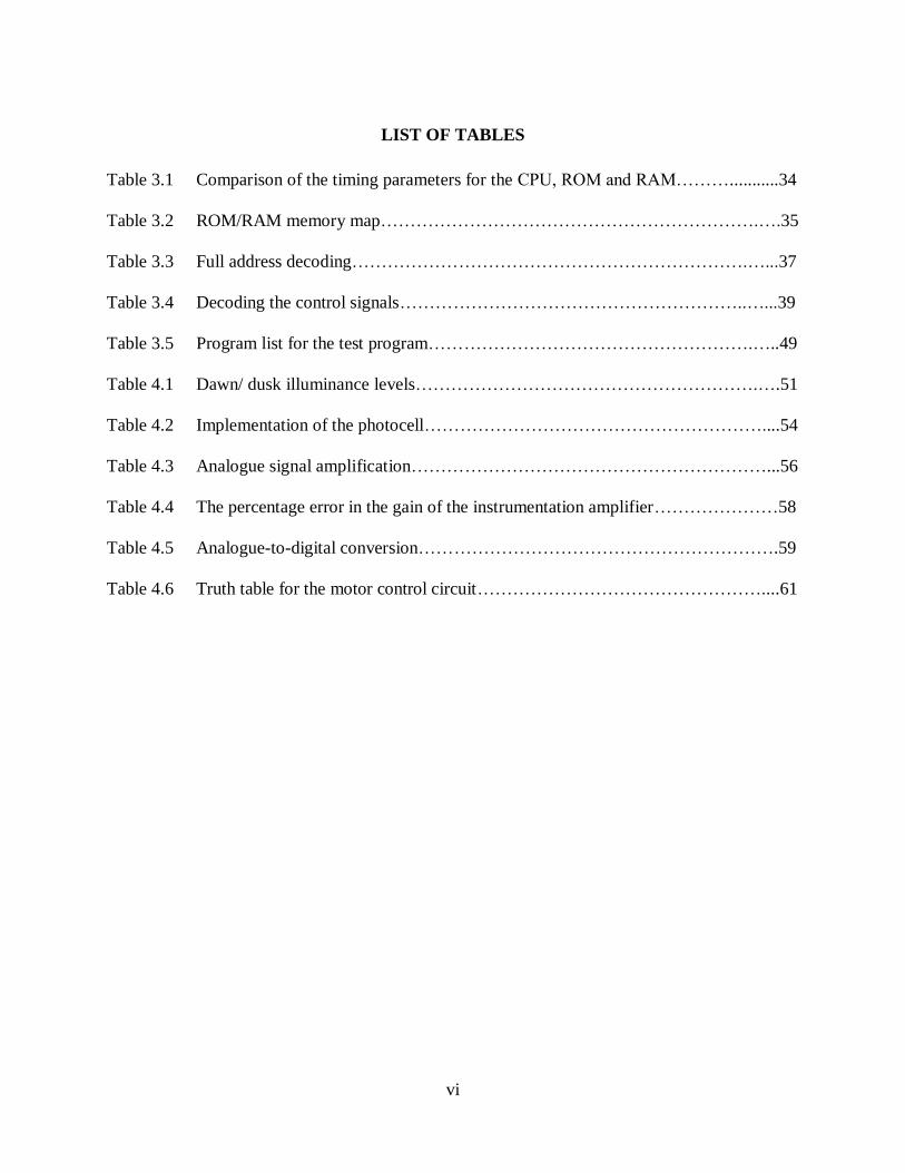
LIST OF TABLES
Table 3.1 Comparison of the timing parameters for the CPU, ROM and RAM………...........34
Table 3.2 ROM/RAM memory map……………………………………………………….….35
Table 3.3 Full address decoding………………………………………………………….…...37
Table 3.4 Decoding the control signals…………………………………………………..…...39
Table 3.5 Program list for the test program……………………………………………….…..49
Table 4.1 Dawn/ dusk illuminance levels………………………………………………….….51
Table 4.2 Implementation of the photocell…………………………………………………....54
Table 4.3 Analogue signal amplification……………………………………………………...56
Table 4.4 The percentage error in the gain of the instrumentation amplifier…………………58
Table 4.5 Analogue-to-digital conversion…………………………………………………….59
Table 4.6 Truth table for the motor control circuit…………………………………………....61
vii
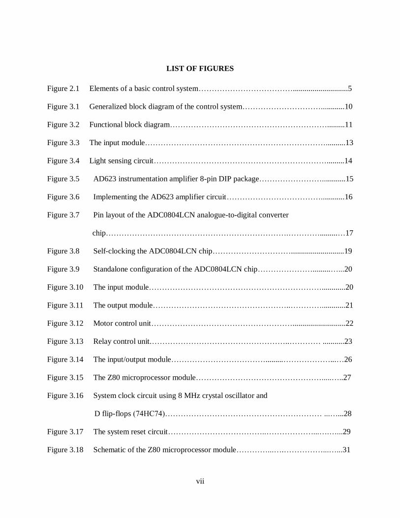
LIST OF FIGURES
Figure 2.1 Elements of a basic control system………………………………............................5
Figure 3.1 Generalized block diagram of the control system…………………………............10
Figure 3.2 Functional block diagram…………………………………………………….........11
Figure 3.3 The input module……………………………………………………………..........13
Figure 3.4 Light sensing circuit………………………………………………………….........14
Figure 3.5 AD623 instrumentation amplifier 8-pin DIP package……………………............15
Figure 3.6 Implementing the AD623 amplifier circuit………………………………............16
Figure 3.7 Pin layout of the ADC0804LCN analogue-to-digital converter
chip…………………………………………………………….………….........…17
Figure 3.8 Self-clocking the ADC0804LCN chip…………………………...........................19
Figure 3.9 Standalone configuration of the ADC0804LCN chip………………….........…...20
Figure 3.10 The input module…………………………………………………………............20
Figure 3.11 The output module……………………………………………..…………............21
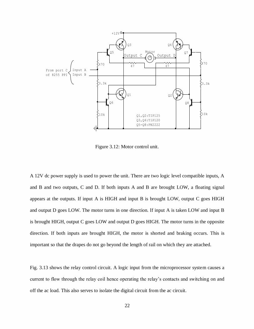
Figure 3.12 Motor control unit………………………………………………...........................22
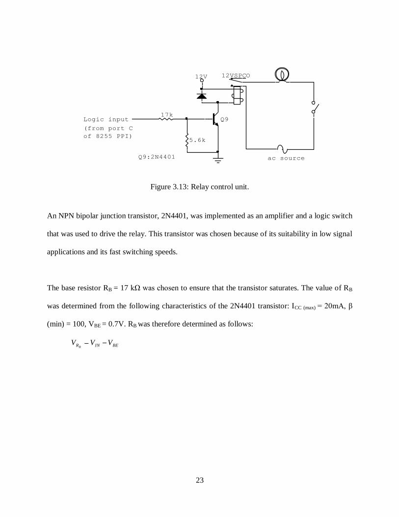
Figure 3.13 Relay control unit.……………………………………………..………… ...........23
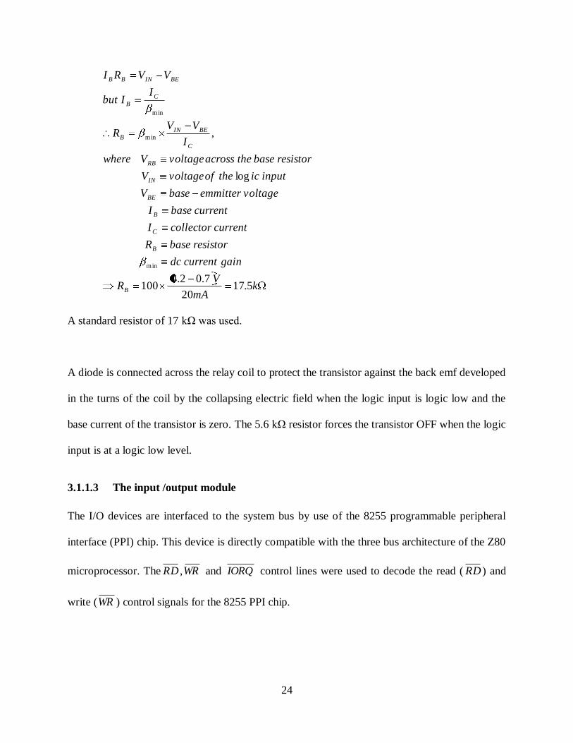
Figure 3.14 The input/output module……………………………….........………………...…26
Figure 3.15 The Z80 microprocessor module………………………………………….....…..27
Figure 3.16 System clock circuit using 8 MHz crystal oscillator and
D flip-flops (74HC74)…………………………………………………… ...…...28
Figure 3.17 The system reset circuit………………………………..………………...….…...29
Figure 3.18 Schematic of the Z80 microprocessor module…………...….……………...…...31
viii
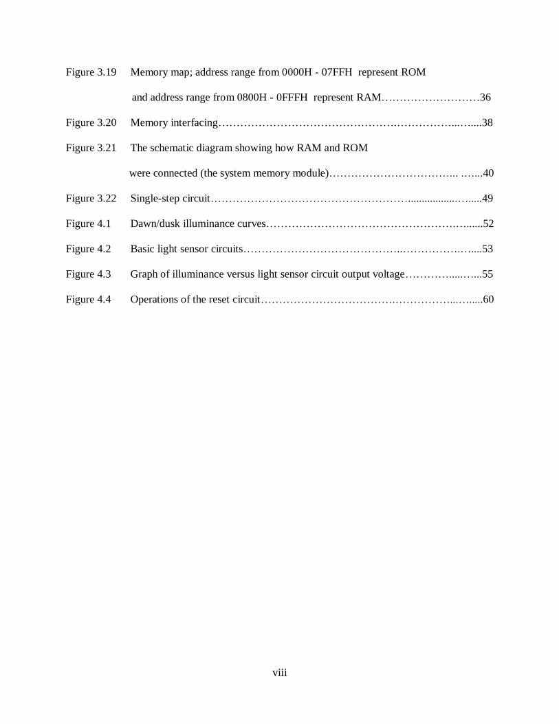
Figure 3.19 Memory map; address range from 0000H - 07FFH represent ROM
and address range from 0800H - 0FFFH represent RAM………………………36
Figure 3.20 Memory interfacing………………………………………….……………...…....38
Figure 3.21 The schematic diagram showing how RAM and ROM
were connected (the system memory module)……………………………... .…...40
Figure 3.22 Single-step circuit………………………………………………..................….....49
Figure 4.1 Dawn/dusk illuminance curves…………………………………………….…......52
Figure 4.2 Basic light sensor circuits……………………………………..…………….…....53
Figure 4.3 Graph of illuminance versus light sensor circuit output voltage………….....…...55
Figure 4.4 Operations of the reset circuit……………………………….……………...….....60

ix
LIST OF APPENDICES
Appendix A Main Circuit Diagram……………………………………………….…...…….71
Appendix B System operating software – Program flow chart………………………...........72
Appendix C System operating software – Assembly and machine language
program.......……………………………………………………………………76

x
ABBREVIATIONS
EPROM Erasable-programmable read-only memory
UV-EPROM Ultra-violet erasable-programmable read-only memory
ROM Read -only memory
RAM Random access memory
SRAM Static random access memory
CPU Central processing unit
MCU Microcontroller unit
MPU Microprocessor unit
PLC Programmable Logic controller
DIP Dual-in-line package
ADC Analogue-to-digital converter
I/O Input/output logic
Ac Alternating current
Dc Direct current
MHz Megahertz
KHz Kilohertz
kB Kilobytes
MB Megabytes
PPI Parallel peripheral interface
PIO Programmable input/output
CdS Cadmium sulphide
xi
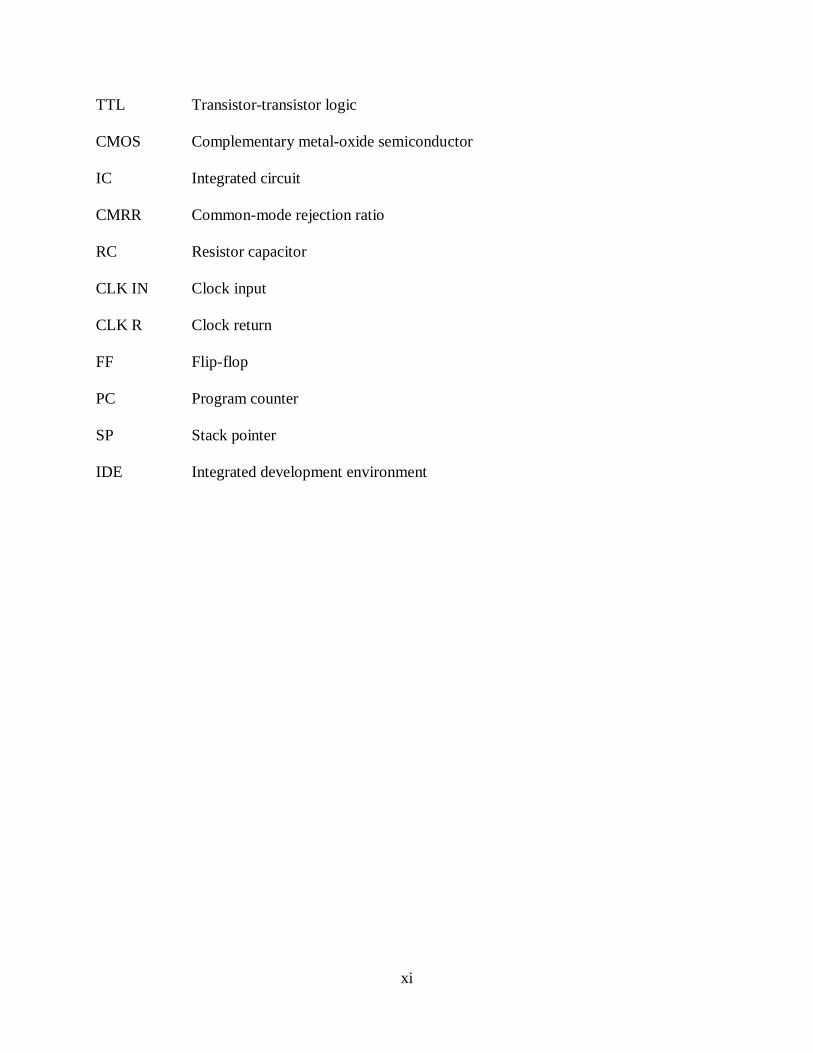
TTL Transistor-transistor logic
CMOS Complementary metal-oxide semiconductor
IC Integrated circuit
CMRR Common-mode rejection ratio
RC Resistor capacitor
CLK IN Clock input
CLK R Clock return
FF Flip-flop
PC Program counter
SP Stack pointer
IDE Integrated development environment
xii
ABSTRACT
The need to automate the various operations found in industries, commercial buildings, and
homes continues to draw much attention to key players in the microelectronics industry. The
development of an automated control system for the control of drapes and security lights and
dependent upon sunlight illuminance levels and time of day is presented. At the heart of the
system is a Z80 microprocessor to control the operations of a motor and an electromagnetic relay
by use of an assembly language control program resident in an EPROM. The system also
comprises one SRAM chip.
Depending on the intensity of sunlight and time of day, drapes will be opened or closed and
security lights will be switched on or off. A cadmium sulphide (CdS) light sensor is used to
collect light and the resulting photocurrent is converted to digital form by an analogue-to-digital
converter (ADC) and then fed to an input/output interface chip after amplification. The Z80
microprocessor chip processes the data collected by use of a software code burnt into a UV-
EPROM chip. An output digital data stream is then used to operate the motor and the
electromagnetic relay.
This study was designed such that when the intensity of sunlight is below 60 lux, drapes will be
closed and security lights switched ON and when the intensity is above 60 lux, drapes will be
opened and security lights switched OFF. This intensity of light corresponds to the time of day
around 6:45 am/pm. The results obtained were found to agree with the design. The system is
designed such that it can be applied to any domestic or industrial setting and can be upgraded to
accommodate more operations.

1
CHAPTER ONE
INTRODUCTION
In today‟s technological world, the microprocessor has found wide applications in control
systems especially in home, office and industrial automation. Virtually any mechanical or
electrical device can be automated. Automation is a step beyond mechanization in that
mechanization involves the use of machines instead of human physical effort while automation
involves turning the machine into self-regulating equipment that can perform an operation
independent of human control.
Modern automated control systems involve the use of a programmable device that works in
accordance with a program (software) that regulates its behaviour. This device may be a
microprocessor unit (MPU), a microcontroller unit (MCU), or a programmable logic controller
(PLC). As the complexity of the target applications vary, there is need to understand each of
these devices in order to decide on the device best suited for a given application. Both an MCU
and a PLC contain a processor, memory, and input/output logic within the same chip. These
devices have a processor that can support only a few instructions (a small instruction set) and a
small memory unit hence they can only support a few programs to perform specific tasks. MCUs
are mainly used in dedicated control systems in which the manufacturer programs the device to
suit a particular function and the software code cannot be altered. PLCs are used for automation
of industrial processes. For this reason, they are designed for severe conditions such as dust,
moisture, cold and heat. They also have a facility for extensive input/output (I/O) arrangements.

2
For a PLC- or MCU-based system, nothing can be done to alter the processor, the memory or the
input/output capability of the device. Consequently, the designer of such a system will need to
have prior knowledge of the device‟s data handling, storage, processing power and
communication capabilities that will suit a particular application. For a microprocessor-based
system, the processor, the memory unit, and the I/O logic are handled separately. The designer of
such a system is at discretion to decide the computing power of the system. The architecture of a
microprocessor-based system is important especially for situations where there is frequent need
to alter the software code (Sunybroome Educational, 2006). The fact that the memory unit and
the processor are separate means that the software code can be written and optimized as often as
required. This makes such a system flexible, expandable, upgradeable, and cost effective (Hai,
2007). For these reasons, microprocessor-based systems have found wide applications in the
automation of home systems such as lighting appliances, heating and air-conditioning,
entertainment appliances, security system and communications. The flexibility, expandability,
and upgradeability provided by a microprocessor-based system makes it easy to program and it
provides a consistent programming interface that would not require learning new programming
techniques every time a new device is added to the system.
This thesis describes a Z80 microprocessor-based system that controls the operation of a direct
current(dc) motor and an electromagnetic relay that are linked to a drapes drawing mechanism
and an alternating current(ac) load respectively. The input to the system is a light source
(sunlight) and the system‟s software code is written based on the sunlight illuminance levels and
the astronomical time (sunrise/sunset). The approach is one of design and then implementation.
3
1.1 Objectives
i. To design and implement an automated light- and time-based control system for drapes
and security lights.
ii. To develop a low cost automated control system.
1.2 Justification
Common routine operations such as gate operations, drapery operations, temperature control and
artificial light control are usually carried out manually. This becomes costly and inconveniencing
because someone may be specifically assigned the task of carrying out these operations. This can
also cause discontinuity in a task being currently performed since a person may disrupt the
current duty to perform the required task. For this reason, ways are being sought to minimize or
eliminate these inconveniences through mechanization and automation.
The physical presence of a home owner to draw the drapes and operate the security lights at dusk
or dawn is not necessary when these operations are automated. The automatic operation gives the
impression that the homeowner is present yet he/she might be absent. The automation of the
mechanism of drawing the drapes through the use of the microprocessor-based control system
can save substantial amounts of electricity by taking advantage of the available sunlight to avoid
the unnecessary use of artificial illumination (Ehrlich et al, 2001; Rubinstein et al, 1989; Popat,
2000).
Simple systems targeting single or a few applications have made use of passive/analogue devices
only to control a given application(s). For instance, a temperature control system can use a

4
temperature sensor and a feedback mechanism to regulate the temperature in a room. The use of
a programmable device in such a system inspires intelligence to the system and hence flexibility
in that the operations of the system can be altered any time by, say changing the system‟s
operating software.
Therefore, there is need to automate the drawing of drapes and the operation of security lights as
this forms part of the common routines performed on daily basis.
5
CHAPTER TWO
LITERATURE REVIEW
2.1 Introduction
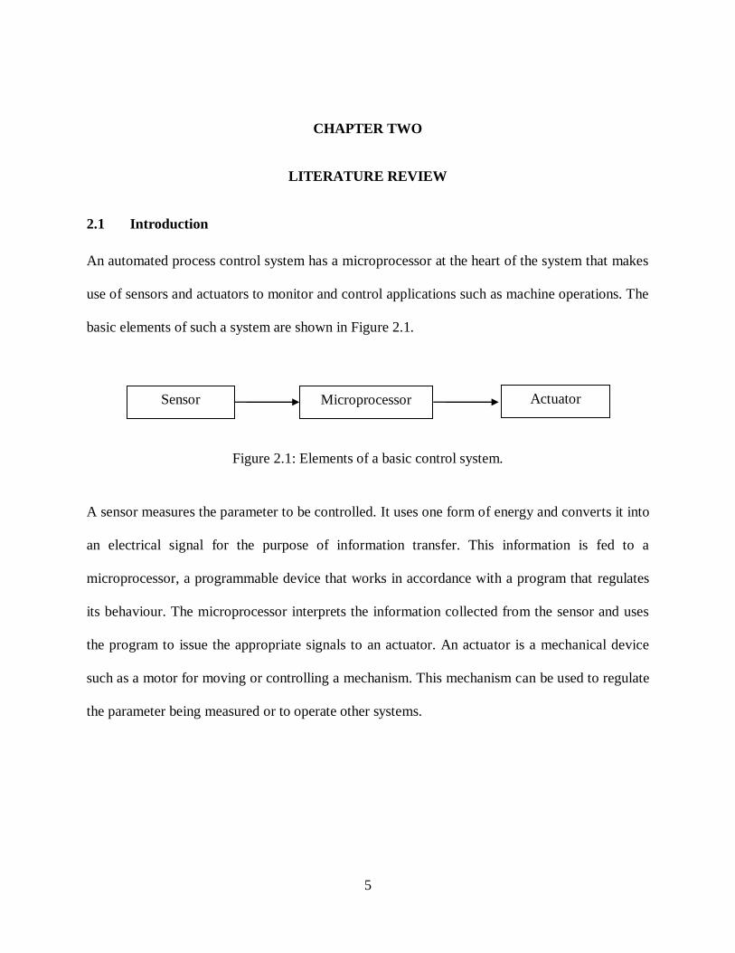
An automated process control system has a microprocessor at the heart of the system that makes
use of sensors and actuators to monitor and control applications such as machine operations. The
basic elements of such a system are shown in Figure 2.1.
Figure 2.1: Elements of a basic control system.
A sensor measures the parameter to be controlled. It uses one form of energy and converts it into
an electrical signal for the purpose of information transfer. This information is fed to a
microprocessor, a programmable device that works in accordance with a program that regulates
its behaviour. The microprocessor interprets the information collected from the sensor and uses
the program to issue the appropriate signals to an actuator. An actuator is a mechanical device
such as a motor for moving or controlling a mechanism. This mechanism can be used to regulate
the parameter being measured or to operate other systems.
Sensor Microprocessor Actuator
6
2.2 Related work
Microprocessors offer a very wide range of instructions so that a microprocessor-based system
can be designed to monitor and control a very wide range of applications (Microchip, 2004;
Sunybroome Educational, 2006). This fact is being utilized in the development of home
automation systems (Hai, 2007; Dewsbury et al, 2003; Cheek et al, 2005) and industrial
automation systems (Gonzalez et al, 2004).
Home automation is a system that gives homeowners the ability to take charge and control
electronic devices even if they are not physically at home. Most home automation systems focus
on security and convenience. Among many other applications, such systems can be made to
automatically operate electric light, set burglar alarms, and operate a gate. However, a special
form of home automation focuses on making it possible for the elderly and disabled to live at
home and still be safe and comfortable (Dewsbury et al, 2003; Cheek et al, 2005).
Shoewu and Baruwa (2006) have developed a home automation system that focuses on
convenience. The system is based on a Z80 microprocessor and is aimed at monitoring and
controlling gate operations. Through an elaborate input/output interface logic using the Z80
parallel input/output interface chips, their work illustrates that the system can be expanded
further to accommodate a very wide range of applications as pertains to home automation
systems. Through an appropriate design, this system can be easily upgraded to use a higher bit
microprocessor to accommodate additional operations and speed optimization.
7
Besides security and convenience, industrial automation systems focus on reducing costs and
optimizing production through the monitoring and control of parameters such as temperature,
humidity, and luminosity (Gonzalez et al, 2004). These parameters, if unchecked, may adversely
affect production through machinery failure, production of low quality goods, and low
productivity from workers as a result of discomfort (Ehrlich et al, 2001; Rubinstein et al, 1989).
Significant effort has been directed to solving problems associated with these parameters.
Gonzalez et al (2004) developed a control system to monitor the changes in the parameters along
an industrial plant. The system is structured into several levels, ranging from a low, direct level
to higher levels (supervision and co-ordination control levels). The direct control level allows
direct interaction with the plant through sensors and having microcontrollers watch over the
measurements taken by the sensors. A supervisory control level allows integration of all the
information about the plant into a single place. The supervisory control level may also involve a
visualization device that allows the user to monitor the conditions occurring in a given zone.
Otieno et al (1997) incorporated an IBM microcomputer to provide a visual indication of raw
data acquired by a Z80 microprocessor system that was used for the automation of a calorimeter.
An adaptive window covering system, a device which automatically self-adjusts to regulate the
light admitted by a window, has been developed by Popat (2000). The device works together
with an adaptive microprocessor-based lighting system to automatically brighten or dim a high
efficiency lamp to maintain a desired level of interior illumination. A similar system by Uddin et
al (2005) makes use of the adaptive lighting system only by incorporating a photosensor to
detect the changes in ambient light and a microcontroller to adjust the intensity of the lamps. In
8
principle, these systems aim at maximizing the natural-to-artificial illumination ratio by
admitting the desired maximum quantity of daylight hence reducing the need for artificial
illumination while still maintaining the desired quality of interior illumination. When used
together, the adaptive window covering system/adaptive lighting system combination has been
found to be more efficient than the use of an adaptive lighting system only (Popat, 2000).
A major challenge in light control systems has been the frequent need to physically adjust a light
sensor so that the illumination detected is a true representative of the illumination of the task
(Rubinstein et al, 1989). To solve this problem, Bierman (2003) developed a lighting control
system that provided the desirable level of lighting at task location by compensating for the
difference in the illuminance ratio for the illumination level at task location to illumination level
at photosensor location. Paton (2007) went a step further by devising a method of remotely
controlling the light and placing a filter on the photo-transducer to match a photopic response
curve (response to sunlight as perceived by the human eye).
Most commercially available photo-transducers respond to a spectrum much wider than the
spectrum perceived by the human eye. Typically, the light in a room has two or more different
contributing light sources such as artificial light and sunlight. A problem arises when
conventional photo-transducers are used in light control systems to detect a given energy
spectrum. When a photo-transducer transforms the captured light energy into a current, it does
not distinguish between different wavelengths of light. Such a control system wrongly assumes
that the current represents visible light. This is a problem because the resultant voltage is derived
from both natural and artificial light components. Piti-goi et al (2007) have developed an

9
illumination management system aimed at solving this problem. The system has a light detection
circuit that uses a photo-transducer to transform captured light into an electrical signal. This
signal is fed to an identification circuit that uses the signal to associate the various light values of
the actual light composition with each light value describing the intensity of the light source. A
correction circuit is used to compare the actual light composition to a desired light composition
and the difference between these two is fed to a light control circuit to adjust ambient light.
There are many control systems that have been developed ranging in complexity from simple
automated systems targeting a single or a few applications, to complex systems targeting
multiple applications. Complex control systems have a microprocessor as the main control unit.
The more complex a system becomes the more powerful is the microprocessor unit required for
the control application and the higher the costs. To lower the costs, it is necessary to develop
custom designed control systems targeting specific applications only as may be found necessary.
This, for instance, may call for the use of a cheap 8-bit microprocessor instead of an expensive
16-bit (or higher) microprocessor. The system described in this thesis is custom designed to
specifically control the operation of drapes and security lights based upon sunlight illuminance
levels and the astronomical time (sunrise/sunset). The system is centred on an 8-bit, 8 MHz Z80
microprocessor chip. To the best of my knowledge, no one has developed such a system before.
10
CHAPTER THREE
METHODOLOGY
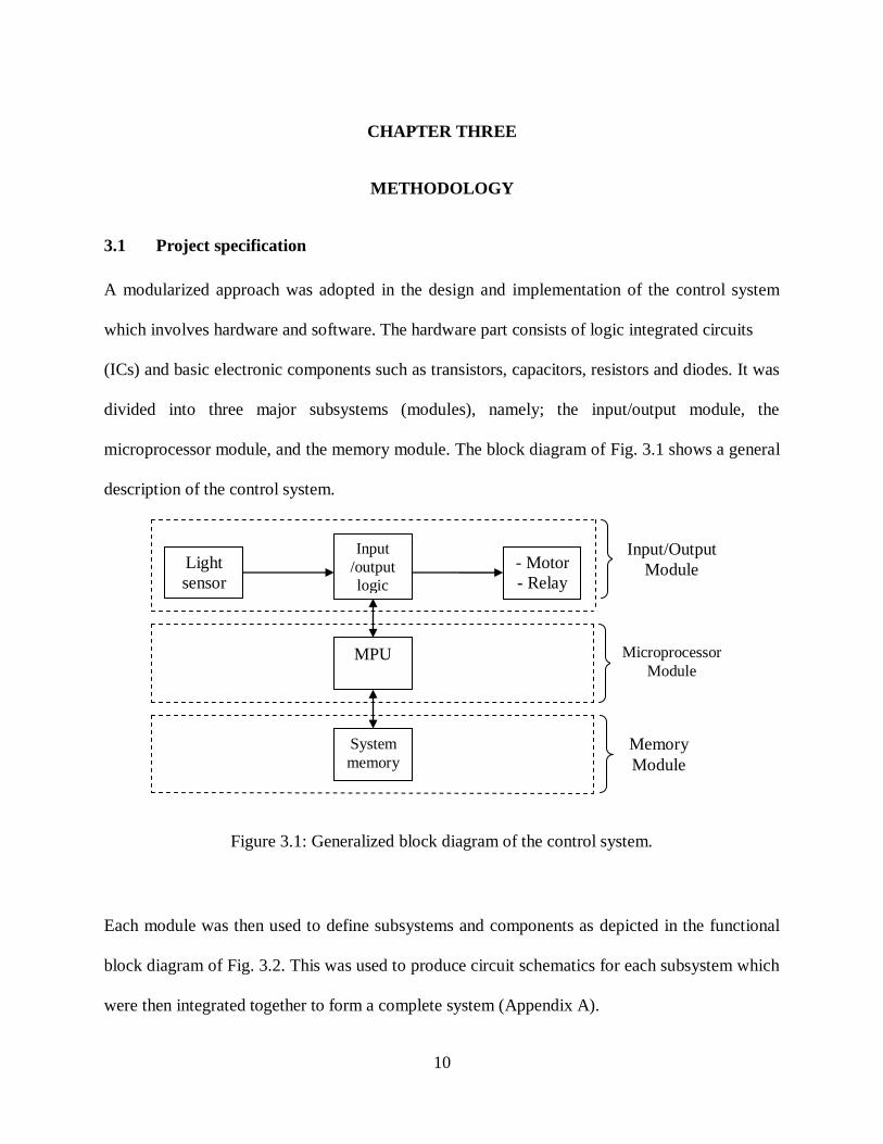
3.1 Project specification
A modularized approach was adopted in the design and implementation of the control system
which involves hardware and software. The hardware part consists of logic integrated circuits
(ICs) and basic electronic components such as transistors, capacitors, resistors and diodes. It was
divided into three major subsystems (modules), namely; the input/output module, the
microprocessor module, and the memory module. The block diagram of Fig. 3.1 shows a general
description of the control system.
Figure 3.1: Generalized block diagram of the control system.
Each module was then used to define subsystems and components as depicted in the functional
block diagram of Fig. 3.2. This was used to produce circuit schematics for each subsystem which
were then integrated together to form a complete system (Appendix A).
MPU
Input
/output
logic
Light
sensor
- Motor
- Relay
System
memory
Input/Output
Module
Microprocessor
Module
Memory
Module
11
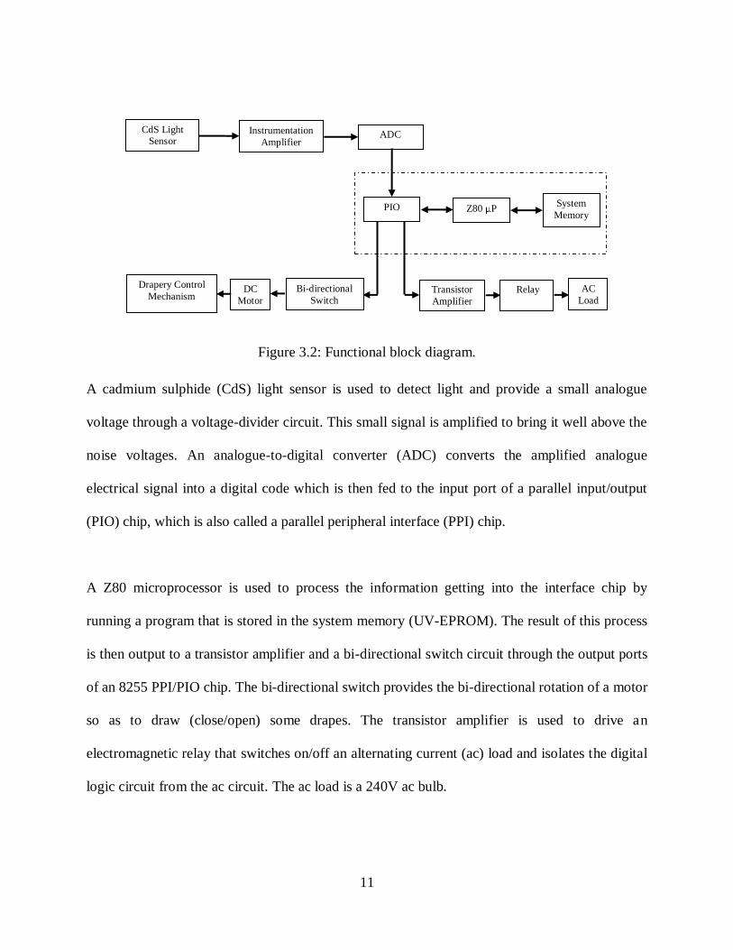
Figure 3.2: Functional block diagram.
A cadmium sulphide (CdS) light sensor is used to detect light and provide a small analogue
voltage through a voltage-divider circuit. This small signal is amplified to bring it well above the
noise voltages. An analogue-to-digital converter (ADC) converts the amplified analogue
electrical signal into a digital code which is then fed to the input port of a parallel input/output
(PIO) chip, which is also called a parallel peripheral interface (PPI) chip.
A Z80 microprocessor is used to process the information getting into the interface chip by
running a program that is stored in the system memory (UV-EPROM). The result of this process
is then output to a transistor amplifier and a bi-directional switch circuit through the output ports
of an 8255 PPI/PIO chip. The bi-directional switch provides the bi-directional rotation of a motor
so as to draw (close/open) some drapes. The transistor amplifier is used to drive an
electromagnetic relay that switches on/off an alternating current (ac) load and isolates the digital
logic circuit from the ac circuit. The ac load is a 240V ac bulb.
CdS Light
Sensor
Instrumentation
Amplifier
ADC
Transistor
Amplifier
PIO
Z80 P
System Memory
Drapery Control
Mechanism
AC
Load
Bi-directional
Switch
DC
Motor
Relay
12
Circuit simulation softwares were used to design the circuit schematics and test their operations.
For the analogue circuits, both SPICE® and TINA® circuit simulation softwares were used,
while for the logic circuits only SPICE® was used to design and test the circuit schematics.
Complementary metal-oxide semiconductor (CMOS) logic ICs were used because they offer
reduced operational costs in the long run owing to their low power consumption compared to
transistor-transistor logic (TTL) ICs. Components were then selected to implement the logic
functions and prototype breadboard designs were built and tested before the components were
incorporated into a single breadboard.
The three major modules and their corresponding subsystems are discussed in section 3.1.1.
3.1.1 The input/output module
In this system, a physical variable-light, is measured and the analogue electrical signal
representing the light data obtained. Since this electrical signal is very small, in the region of
noise voltages, an instrumentation amplifier is used to amplify it to bring it well above the noise
voltages. A microprocessor system is designed to handle digital data. Therefore, the amplified
analogue electrical signal is converted to digital form for onward transmission to the
microprocessor system. The digital output signals from the microprocessor system are used to
operate analogue devices.
Each of the modules that make up the input/output module is discussed in the subsections that
follow.
13
3.1.1.1 The input module
This module involves the collection of light intensity and its conversion to an electrical signal,
the amplification of the electrical signal obtained, and its conversion to digital form. This is
depicted in the block diagram of Fig. 3.3.
Figure 3.3: The input module.
The CdS photocell was selected in preference to photodiodes and phototransistors because its
characteristics are generally excellent for the target application, notably: a spectral response that
is close to that of the human eye, very good sensitivity to the visible spectrum, and excellent
performance-to-cost ratio.
The light sensing circuit is shown in Fig. 3.4. This consists of a CdS photocell and a 24 kΩ
resistor arranged to form a voltage divider circuit.
CdS photocell Instrumentation
amplifier
ADC Light
intensity
do
d1 dm-1
14
CdS photocell
Vo
Vin
+5V
R
24k
Rp
Vin
+5V
R
24k
Rp
Figure 3.4: Light sensing circuit.
The resistance, RP, of a photocell increases with decrease in light intensity and decreases with
increase in light intensity. Therefore, with decrease in light intensity, RP will increase and the
output voltage, VO, will increase accordingly (since IRV ). Similarly, with an increase in light
intensity, RP will decrease and VO will decrease accordingly.
An instrumentation amplifier whose pin-out is shown in Fig. 3.5 is used to amplify the analogue
electrical signal obtained from the light sensor circuit. An instrumentation amplifier is designed
with several op amps and precision resistors which make the circuit extremely stable and useful
where performance and precision are required. This makes it the most useful amplifier for
instrumentation and control.
15
IN+IN- V+
V-OUTREF
RGRG
AD623
IN+IN- V+
V-OUTREF
RGRG
AD623
Figure 3.5: AD623 instrumentation amplifier 8-pin DIP package.
With no external resistor, the instrumentation amplifier chip, AD623 is configured for unity gain
(G = 1). With an external resistor (gain resistor, RG), the AD623 can be programmed for gains of
up to 1,000. For a certain desired gain, RG is calculated using Equation 3.1.
1
100
G
kRG
…………………………………………………………………………... (3.1)
Where,
gaindesiredG
valueresistorgainRG
The AD623 instrumentation amplifier was implemented as shown in Fig. 3.6.
16
(from the output
of the light
sensing circuit)
Output voltage
(to ADC0804LCN)
Input
voltage
+5V
+10uF
0.1uF
3IN+
2IN-
7V+
4V-
6OUT
5REF
8RG
1RG
AD623
RG100k
Figure 3.6: Implementing the AD623 amplifier circuit.
Pin 7 was connected to +5V while pin 4 was grounded. The +5V input was capacitively
decoupled using a 0.1 µF ceramic capacitor and a 10 µF aluminium electrolytic capacitor. The
input voltage fed to the IN+ input pin of the AD623 was derived from the light sensor output
voltage, VO, while the IN- input was grounded. The frequency of the input signal was measured
by use of an oscilloscope and found to be approximately 100 HZ. This means that the common-
mode rejection ratio (CMRR) remains constant (noise is rejected when the CMRR remains
constant for frequencies up to 200 Hz). A gain of 2 was found to be sufficient and the value of
RG = 100 kΩ was determined using Equation (3.1). Therefore, a 100 kΩ 1% tolerance resistor
was connected to the RG terminals.
The analogue-to-digital converter chip, ADC0804LCN is used to convert the amplified analogue
electrical signal to an 8-bit digital code. This is necessary because the microprocessor is a digital
system and can only process digital data. The ADC0804LCN chip has a resolution of 8 bits. This
17
makes it relatively chip and provides an easy interface to the 8-bit data bus of the Z80
microprocessor. The chip uses successive approximation method and it is primarily designed for
use with a microprocessor system. This means that its digital output pins are in a high impedance
state unless the RD (read) pin is pulled low. The chip is also disabled unless the CS (chip select)
pin is pulled low. Fig. 3.7 shows the pin layout of the ADC0804LCN.
Figure 3.7: Pin layout of the ADC0804LCN analogue-to-digital converter chip.
The control application in this project requires that the system processes an 8-bit digital word
corresponding to a given light data and interprets it as either darkness or light. Consequently, the
ADC was implemented as a comparator to determine whether an analogue input is greater than
or less than a fixed reference DC value, thereby giving an all 0s or all 1s 8-bit output word. This
was accomplished by grounding the VREF/2 pin (to provide maximum resolution) and applying a
2.5V reference DC voltage to the VIN (-) input.

18
The ADC0804LCN chip is designed to operate at a clock frequency (fclk) range of 100 kHz to 1
MHz with a typical value of 640 kHz when operated at VCC = 5V. However, the Z80
microprocessor unit is being operated at a clock frequency of 2 MHz. Consequently, the ADC
could not be connected to the system‟s control bus. For this reason, it was implemented into the
system in a standalone configuration with special consideration on the chip‟s control signals and
making use of its internal clock generator.
The chip was enabled by pulling the CS (Chip Select) input low. By connecting to digital
ground, the RD input was also kept grounded to provide the Output Enable function such that
the latest conversion always appears at the outputs. The start conversion control pin,WR , causes
a conversion to begin. When the conversion is finished, a low level appears on the
INTR (Interrupt Request) pin to signal that fact. This does not have to cause an interrupt, but can
merely be sampled to find out the converter status. Due to the standalone configuration adopted,
the INTR output pin was connected to the WR input pin so that the end of each conversion began
a new one and the converter always displayed the latest conversion at its output. Further, to
trigger the chip‟s start function, the INTR /WR connection was forced to a logic low upon
power-up.
The internal clock generator is used to self-clock the chip. This was accomplished by creating an
external RC oscillator and making use of the CLK R and CLK IN pins. Data sheets of ADC0804
LCN analogue-to-digital converter IC give the recommended values for the capacitor and the
resistor as 150 pF and 10 kΩ respectively. The self-clocking circuit is shown in Fig. 3.8.

19
CLK R CLK IN10k
150pF
10k
150pF
Figure 3.8: Self-clocking the ADC0804LCN chip.
The RC oscillator with the resistor and capacitor values shown provides a clock frequency of
about 646 kHz, with the frequency of the CLK R pin about 331 kHz; while that at the CLK IN
pin about 315 kHz. Summing up the two frequencies gives 646 kHz which is within the chip‟s
clock frequency range (100 kHz – 1 MHz) and very close to the typical value of 640 kHz.
The analogue signal from the amplifier circuit (Fig. 3.6) is applied to the VIN (+) input. The VCC
pin is bypassed by a 10 µF capacitor to keep the power supply steady. The standalone connection
of the ADC0804LCN chip is shown in Fig. 3.9.
20
msb
lsb
Analogue ground
Digital ground
Analogue
input
(from amplifier
circuit)
+5V
+5V
150pF
10uF
ADC0804CS
P1RD
P2WRP3
CLKRP4
INTP5 Vplu
P6 Vmnu
P7A GNDP8Vref
P9D GND
P10D0
P11
D1P12
D2P13
D3P14
D4P15
D5P16
D6P17
D7P18
CLKINP19
VccP20 10k
1k1k
Figure 3.9: Standalone configuration of the ADC0804LCN chip.
The complete schematic diagram of the input module is presented in Fig. 3.10.
8-bit
output
code
msb
lsb
Analogue ground
Digital ground
24k+10uF
0.1uF
3IN+
2IN-
7V+
4V-
6OUT5
REF
8RG
1RG
AD623
+5V +5V
ADC0804CS
P1RDP2WRP3
CLKRP4
INTP5
VpluP6 Vmnu
P7A GND
P8VrefP9D GNDP10 D0P11
D1P12
D2P13
D3P14
D4P15
D5P16
D6P17
D7P18
CLKINP19
VccP20
10uF
150pF
+5V
+5V
RG100k
1k1k
10k
Figure 3.10: The input module.
21
3.1.1.2 The output module
This module involves the use of the digital output signals of the microprocessor system to drive
the output devices. Transistor amplifiers are used to amplify the signals from the microprocessor
system and hence provide the drive current necessary to operate a dc motor and an
electromagnetic relay. The transistors that drive the motor are arranged in such a manner that the
motor can rotate in either direction by reversing the polarity at the motor‟s terminals. The motor
is then made to operate a mechanism the draw drapes. The relay is used to switch on and off an
ac load (240V ac security lights) while isolating the digital logic circuit from the ac circuit. Fig.
3.11 shows the block diagram of the output module.
Figure 3.11: The output module.
Fig. 3.12 shows the motor control unit. Each pair consists of a bipolar junction transistor (BJT)
and a Darlington transistor (e.g. Q6 and Q1) such that the Darlington transistor amplifies the
effect of the BJT. The set of transistors Q5, Q3 and Q6, Q1 controls the motion of the motor in
one direction while the other set consisting of Q7, Q4 and Q8, Q2 controls the rotation of the
motor in the opposite direction. The resistors serve to bias the transistors. The motor used is a
12V electric dc motor that has the ability to rotate in both directions by reversing the polarity.
Transistor
amplifier
Bi-directional
switch DC
motor
Electromagnetic
relay Ac load
Digital
electronic
signals
Drapes control
mechanism
22
Output DOutput C
Input A
Input B
Q1,Q2:TIP125
Q3,Q4:TIP120
Q5-Q8:PN2222
From port C
of 8255 PPI
470
3.3k
10k
4747470
3.3k
10k
Motor
Q8
Q7
Q6
Q5
Q2Q1
Q3 Q4
+12V
Figure 3.12: Motor control unit.
A 12V dc power supply is used to power the unit. There are two logic level compatible inputs, A
and B and two outputs, C and D. If both inputs A and B are brought LOW, a floating signal
appears at the outputs. If input A is HIGH and input B is brought LOW, output C goes HIGH
and output D goes LOW. The motor turns in one direction. If input A is taken LOW and input B
is brought HIGH, output C goes LOW and output D goes HIGH. The motor turns in the opposite
direction. If both inputs are brought HIGH, the motor is shorted and braking occurs. This is
important so that the drapes do not go beyond the length of rail on which they are attached.
Fig. 3.13 shows the relay control circuit. A logic input from the microprocessor system causes a
current to flow through the relay coil hence operating the relay‟s contacts and switching on and
off the ac load. This also serves to isolate the digital circuit from the ac circuit.
23
Logic input
Q9:2N4401
(from port C
of 8255 PPI)
17k
5.6k
ac source
12V
Q9
12VSPCO
Figure 3.13: Relay control unit.
An NPN bipolar junction transistor, 2N4401, was implemented as an amplifier and a logic switch
that was used to drive the relay. This transistor was chosen because of its suitability in low signal
applications and its fast switching speeds.
The base resistor RB = 17 kΩ was chosen to ensure that the transistor saturates. The value of RB
was determined from the following characteristics of the 2N4401 transistor: ICC (max) = 20mA, β
(min) = 100, VBE = 0.7V. RB was therefore determined as follows:
BEINR VVVB
24
kmA
VR
gaincurrentdc
resistorbaseR
currentcollectorI
currentbaseI
voltageemmitterbaseV
inputictheofvoltageV
resistorbasetheacrossvoltageVwhere
I
VVR
IIbut
VVRI
B
B
C
B
BE
IN
RB
C
BEINB
C
B
BEINBB
5.1720
7.02.4100
log
,
min
min
min
A standard resistor of 17 kΩ was used.
A diode is connected across the relay coil to protect the transistor against the back emf developed
in the turns of the coil by the collapsing electric field when the logic input is logic low and the
base current of the transistor is zero. The 5.6 kΩ resistor forces the transistor OFF when the logic
input is at a logic low level.
3.1.1.3 The input /output module
The I/O devices are interfaced to the system bus by use of the 8255 programmable peripheral
interface (PPI) chip. This device is directly compatible with the three bus architecture of the Z80
microprocessor. The RD ,WR and IORQ control lines were used to decode the read ( RD ) and
write (WR ) control signals for the 8255 PPI chip.

25
The 8255 PPI was initialized to operate in a basic input/output configuration that allows simple
input/output operations. It has three ports: A, B and C, which can be programmed as input and/or
output. In this research we have used port A as input and port C as output. Port B is unused.
The 8255 PPI was configured in the input/output mapped input/output configuration. The eight
output bits of the ADC were fed to the eight pins (PA0 – PA7) of port A while pins PC0 and PC1
of port C were fed to the two inputs of the motor control unit. The logic input of the relay unit
was obtained from pin PC7 of port C.
Connection of the input and output modules to the 8255 PPI is shown in Fig. 3.14.
26
BA
Q9:2N4401
Q1,Q2:TIP125
Q3,Q4:TIP120
Q5-Q8:PN2222
msb
lsb
Digital ground
Analogue ground
A0
A1
System
reset
RD
IORQ
WR
Input B
Input A
24k Q4Q3
+5V +12V
12VSPCO
Q9
12V
ac source
Q1Q2
Q5
Q6
Q7
Q8
Motor
+5V
+
10uF
0.1uF
3IN+
2IN- 7V+
4V-
6OUT
5REF
8RG1RG
AD623
ADC0804CSP1RD
P2WRP3
CLKRP4INT
P5 VpluP6 Vmnu
P7A GND
P8Vref
P9D GNDP10 D0P11
D1P12
D2P13
D3P14
D4P15
D5P16
D6P17
D7P18
CLKINP19
VccP20
10uF
150pF
+5V
+5V
8255 PPI
PA3P1
PA2P2
PA1P3PA0P4
RDP5CSP6
GNDP7
A1P8
A0P9PC7P10PC6P11
PC5P12PC4P13
PC0P14PC1P15
PC2P16PC3P17
PB0P18
PB1P19
PB2P20
PB3P21
PB4P22
PB5P23
PB6P24
PB7P25
VccP26
D7P27
D6P28
D5P29
D4P30
D3P31
D2P32
D1P33
D0P34
RESETP35
WRP36
PA7P37
PA6P38
PA5P39
PA4P40
+5V
5.6k
17k
10k
3.3k
470 47 47
10k
3.3k
470
RG 100k
1k1k
10k
Figure 3.14: The input/output module.
3.1.2 The Z80 microprocessor module
This module establishes the basic system timing, provides an orderly means of starting up the
microprocessor, and provides access to the system buses. The main components that were used
to achieve these functions are: a Z80 CPU, a clock generator circuit, and a reset circuit. This is
illustrated in the block diagram of Fig. 3.15.
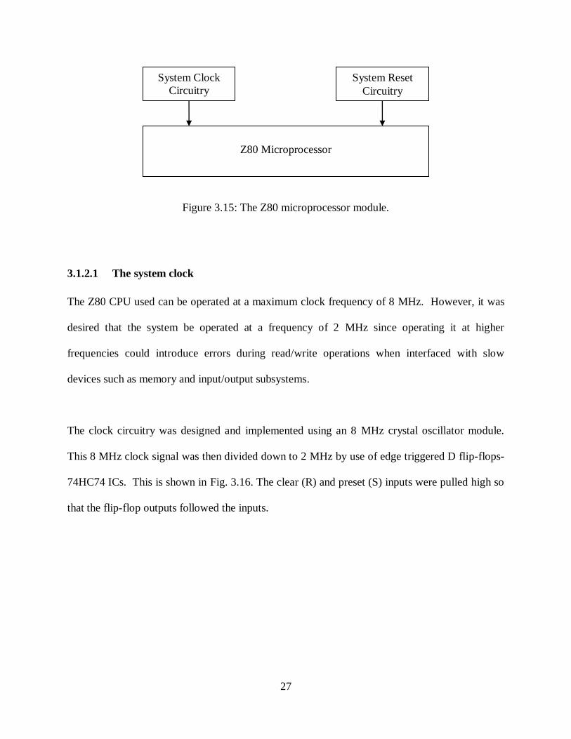
27
Figure 3.15: The Z80 microprocessor module.
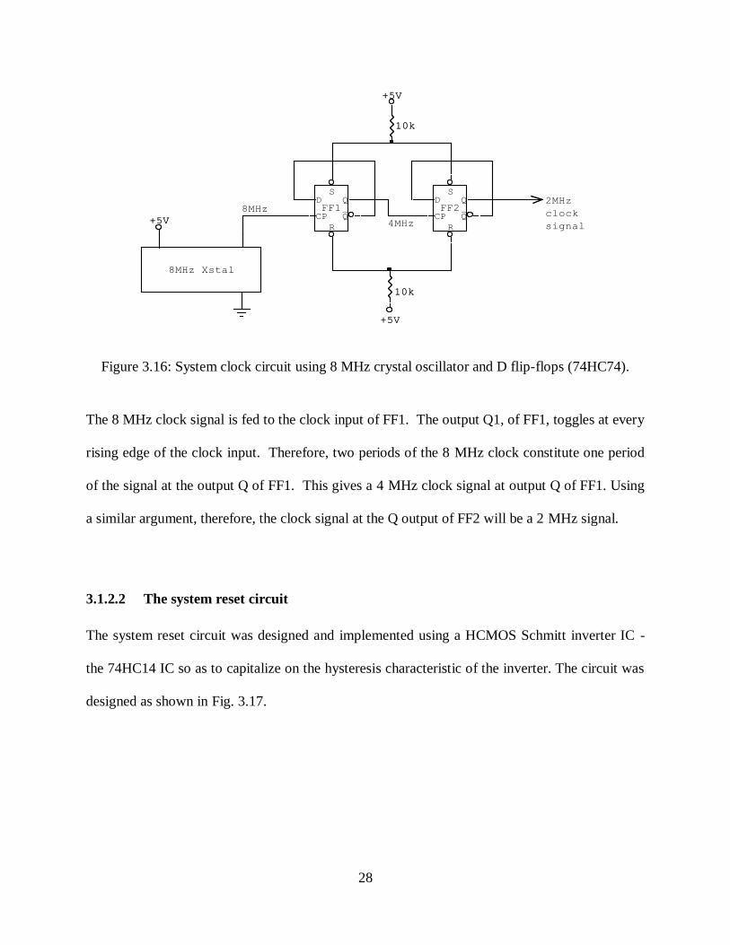
3.1.2.1 The system clock
The Z80 CPU used can be operated at a maximum clock frequency of 8 MHz. However, it was
desired that the system be operated at a frequency of 2 MHz since operating it at higher
frequencies could introduce errors during read/write operations when interfaced with slow
devices such as memory and input/output subsystems.
The clock circuitry was designed and implemented using an 8 MHz crystal oscillator module.
This 8 MHz clock signal was then divided down to 2 MHz by use of edge triggered D flip-flops-
74HC74 ICs. This is shown in Fig. 3.16. The clear (R) and preset (S) inputs were pulled high so
that the flip-flop outputs followed the inputs.
System Clock
Circuitry
System Reset
Circuitry
Z80 Microprocessor
28
8MHz2MHz
clock
signal4MHz
+5V
+5V
10k
10k
+5V
SD
CP
R
Q_Q
FF2
SD
CP
R
Q_Q
FF1
8MHz Xstal
+5V
+5V
10k
10k
+5V
SD
CP
R
Q_Q
FF2
SD
CP
R
Q_Q
FF1
8MHz Xstal
Figure 3.16: System clock circuit using 8 MHz crystal oscillator and D flip-flops (74HC74).
The 8 MHz clock signal is fed to the clock input of FF1. The output Q1, of FF1, toggles at every
rising edge of the clock input. Therefore, two periods of the 8 MHz clock constitute one period
of the signal at the output Q of FF1. This gives a 4 MHz clock signal at output Q of FF1. Using
a similar argument, therefore, the clock signal at the Q output of FF2 will be a 2 MHz signal.
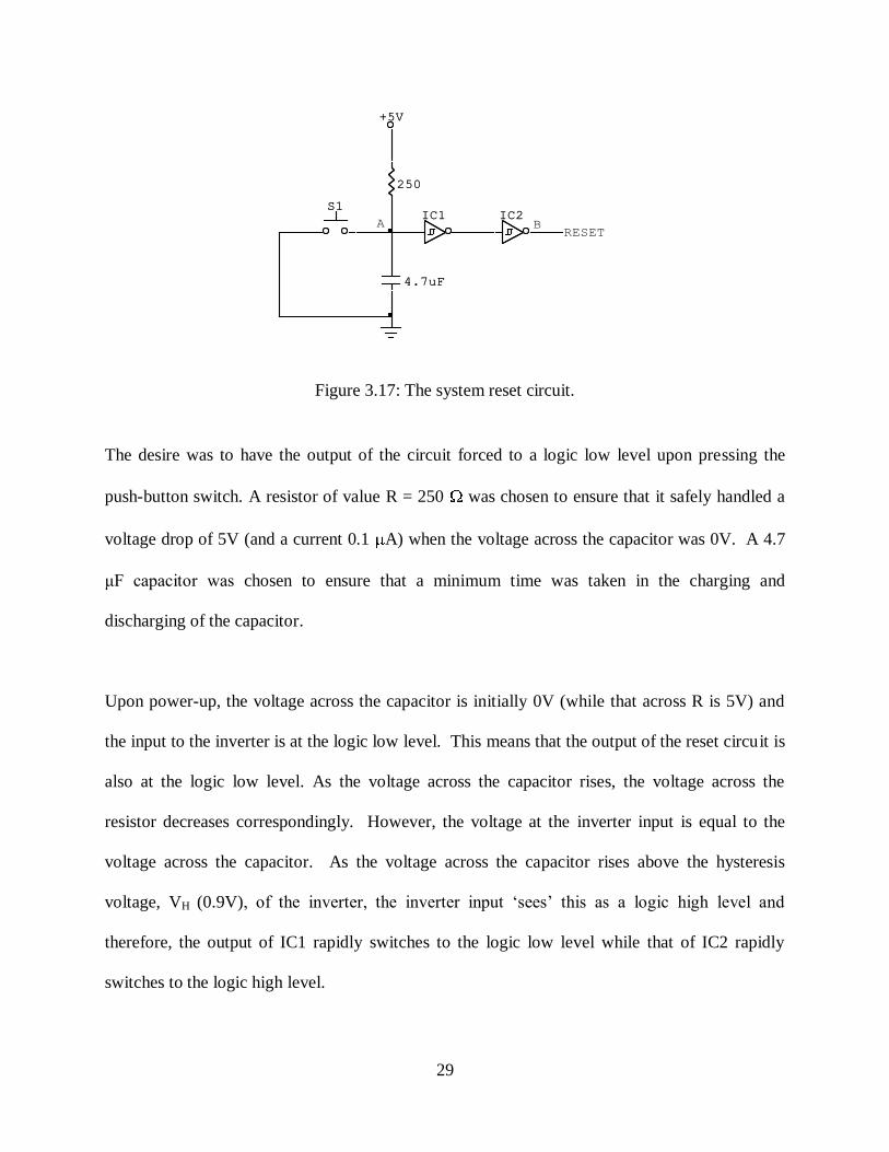
3.1.2.2 The system reset circuit
The system reset circuit was designed and implemented using a HCMOS Schmitt inverter IC -
the 74HC14 IC so as to capitalize on the hysteresis characteristic of the inverter. The circuit was
designed as shown in Fig. 3.17.
29
RESETA B
+5V
S1
250
4.7uF
IC1 IC2
+5V
S1
250
4.7uF
IC1 IC2
Figure 3.17: The system reset circuit.
The desire was to have the output of the circuit forced to a logic low level upon pressing the
push-button switch. A resistor of value R = 250 was chosen to ensure that it safely handled a
voltage drop of 5V (and a current 0.1 A) when the voltage across the capacitor was 0V. A 4.7
μF capacitor was chosen to ensure that a minimum time was taken in the charging and
discharging of the capacitor.
Upon power-up, the voltage across the capacitor is initially 0V (while that across R is 5V) and
the input to the inverter is at the logic low level. This means that the output of the reset circuit is
also at the logic low level. As the voltage across the capacitor rises, the voltage across the
resistor decreases correspondingly. However, the voltage at the inverter input is equal to the
voltage across the capacitor. As the voltage across the capacitor rises above the hysteresis
voltage, VH (0.9V), of the inverter, the inverter input „sees‟ this as a logic high level and
therefore, the output of IC1 rapidly switches to the logic low level while that of IC2 rapidly
switches to the logic high level.

30
Resetting the circuit is accomplished by forcing the circuit output to the logic low level. This is
done by pressing the push-button switch, S1. The effect of this is to short the capacitor to
ground, thereby discharging it, and forcing the input of IC1 to the logic low level and thus giving
a logic low level output at the circuit output.
3.1.2.3 The Z80 microprocessor - Z84C0008PEC CPU
The Z84C0008PEC CPU is an 8-bit CMOS version of the Z80 family of microprocessors. It is
designed to operate at a maximum clock rate of 8 MHz.
All the unused input pins were pulled high by use of 10 kΩ resistors so as to avoid the possibility
of having noise at the inputs. These input pins are BUSREQ , WAIT , NMI and INT . For the
same reason all the data lines and address lines were pulled high by use of 10 kΩ resistors.
The circuit for the Z80 microprocessor module was designed and implemented as shown in Fig.
3.18.
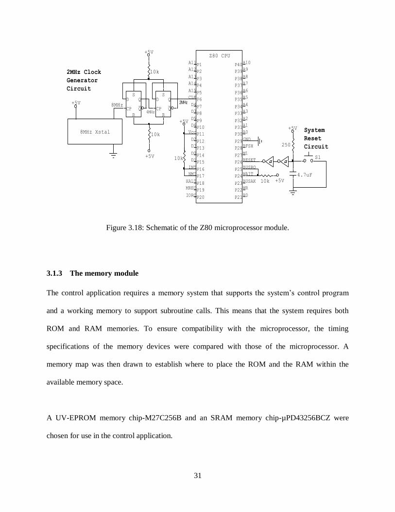
31
2MHz Clock
Generator
Circuit
System
Reset
Circuit
8MHz2MHz
4MHz
+5V
+5V
+5V
S1
4.7uF
+5V
+5V
+5V
SD
CP
R
Q_Q
SD
CP
R
Q_Q
8MHz Xstal
Z80 CPU
A11P1A12P2A13
P3A14P4A15
P5CLKP6
D4P7D3
P8D5P9D6
P10VccP11D2
P12D7P13
D0P14D1
P15INTP16NMI
P17HALTP18MREQ
P19IORQ
P20RD
P21
WRP22
BUSAKP23
WAITP24
BUSRQP25
RESETP26
M1P27
RFSHP28
GNDP29
A0P30
A1P31
A2P32
A3P33
A4P34
A5P35
A6P36
A7P37
A8P38
A9P39
A10P40
10k
10k
250
10k
10k
Figure 3.18: Schematic of the Z80 microprocessor module.
3.1.3 The memory module
The control application requires a memory system that supports the system‟s control program
and a working memory to support subroutine calls. This means that the system requires both
ROM and RAM memories. To ensure compatibility with the microprocessor, the timing
specifications of the memory devices were compared with those of the microprocessor. A
memory map was then drawn to establish where to place the ROM and the RAM within the
available memory space.
A UV-EPROM memory chip-M27C256B and an SRAM memory chip-µPD43256BCZ were
chosen for use in the control application.
32
The M27C256B ROM chip is a 256 kbit CMOS UV-EPROM and is organized as 32,768 by 8
bits (32kb × 8). The chip has address lines A0 through A14 and data lines D0 through D7 that
connect directly to the chip. The µPD43256BCZ is a 256 kbit (32,768 words by 8 bits) CMOS
static RAM. The chip has 15 address inputs (AO - A14) and 8 bidirectional data pins (I/01 -
I/08).
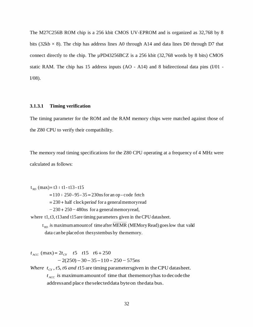
3.1.3.1 Timing verification
The timing parameter for the ROM and the RAM memory chips were matched against those of
the Z80 CPU to verify their compatibility.
The memory read timing specifications for the Z80 CPU operating at a frequency of 4 MHz were
calculated as follows:
memory. by the bus system on the placed becan data
d that valilow goes Read)(MEMory MEMRafter timeofamount maximumst
datasheet. CPU in thegiven parameters timingare t15and t13 t3, t1,where
read,memory general afor 480ns250230
readmemory general afor perioclock half230
fetch code-opan for 230ns35-95-250110
t15-t13-t1t3 (max) t
RD
RD
i
d
bus. data on the byte data selected theplace and address
thedecode tohasmemory that the timeofamount maximums
datasheet. CPU in thegiven parameters timingare156,5,
5752501103530)250(2
25061552(max)
it
tandtttWhere
ns
ttttt
ACC
CY
CYACC
33
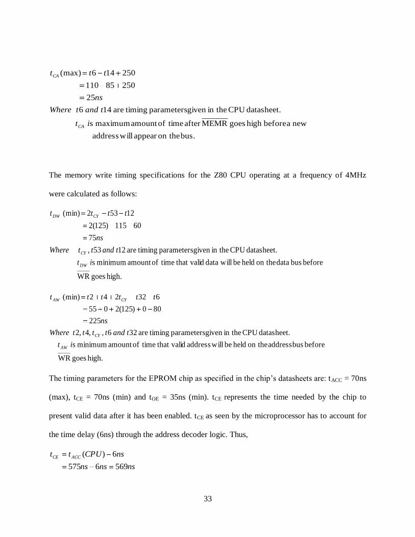
bus. on theappear willaddress
new a beforehigh goes MEMRafter timeofamount maximums
datasheet. CPU in thegiven parameters timingare146
25
25085110
250146(max)
it
tandtWhere
ns
ttt
CA
CA
The memory write timing specifications for the Z80 CPU operating at a frequency of 4MHz
were calculated as follows:
high. goes WR
before bus data on the held be willdata d that vali timeofamount minimums
datasheet. CPU in thegiven parameters timingare1253,
75
60115)125(2
12532(min)
it
tandttWhere
ns
tttt
DW
CY
CYDW
high. goes WR
before bus address on the held be willaddress d that vali timeofamount minimums
datasheet. CPU in thegiven parameters timingare326,,4,2
225
800)125(2055
632242(min)
it
tandttttWhere
ns
tttttt
AW
CY
CYAW
The timing parameters for the EPROM chip as specified in the chip‟s datasheets are: tACC = 70ns
(max), tCE = 70ns (min) and tOE = 35ns (min). tCE represents the time needed by the chip to
present valid data after it has been enabled. tCE as seen by the microprocessor has to account for
the time delay (6ns) through the address decoder logic. Thus,
nsnsns
nsCPUtt ACCCE
5696575
6)(
34
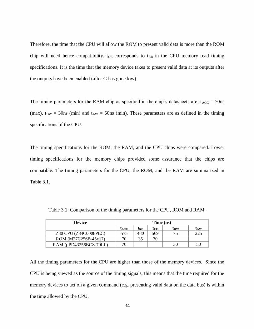
Therefore, the time that the CPU will allow the ROM to present valid data is more than the ROM
chip will need hence compatibility. tOE corresponds to tRD in the CPU memory read timing
specifications. It is the time that the memory device takes to present valid data at its outputs after
the outputs have been enabled (after G has gone low).
The timing parameters for the RAM chip as specified in the chip‟s datasheets are: tACC = 70ns
(max), tDW = 30ns (min) and tAW = 50ns (min). These parameters are as defined in the timing
specifications of the CPU.
The timing specifications for the ROM, the RAM, and the CPU chips were compared. Lower
timing specifications for the memory chips provided some assurance that the chips are
compatible. The timing parameters for the CPU, the ROM, and the RAM are summarized in
Table 3.1.
Table 3.1: Comparison of the timing parameters for the CPU, ROM and RAM.
Device Time (ns)
tACC tRD tCE tDW tAW
Z80 CPU (Z84C0008PEC) 575 480 569 75 225
ROM (M27C256B-45x17) 70 35 70
RAM ( PD43256BCZ-70LL) 70 30 50
All the timing parameters for the CPU are higher than those of the memory devices. Since the
CPU is being viewed as the source of the timing signals, this means that the time required for the
memory devices to act on a given command (e.g. presenting valid data on the data bus) is within
the time allowed by the CPU.
35
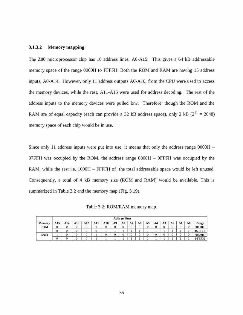
3.1.3.2 Memory mapping
The Z80 microprocessor chip has 16 address lines, A0-A15. This gives a 64 kB addressable
memory space of the range 0000H to FFFFH. Both the ROM and RAM are having 15 address
inputs, A0-A14. However, only 11 address outputs A0-A10, from the CPU were used to access
the memory devices, while the rest, A11-A15 were used for address decoding. The rest of the
address inputs to the memory devices were pulled low. Therefore, though the ROM and the
RAM are of equal capacity (each can provide a 32 kB address space), only 2 kB (211
= 2048)
memory space of each chip would be in use.
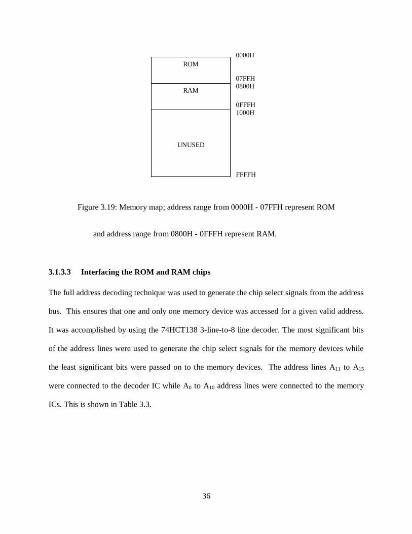
Since only 11 address inputs were put into use, it means that only the address range 0000H –
07FFH was occupied by the ROM, the address range 0800H – 0FFFH was occupied by the
RAM, while the rest i.e. 1000H – FFFFH of the total addressable space would be left unused.
Consequently, a total of 4 kB memory size (ROM and RAM) would be available. This is
summarized in Table 3.2 and the memory map (Fig. 3.19).
Table 3.2: ROM/RAM memory map.
Address lines Memory A15 A14 A13 A12 A11 A10 A9 A8 A7 A6 A5 A4 A3 A2 A1 A0 Range
ROM 0 0 0 0 0 0 0 0 0 0 0 0 0 0 0 0 0000H
0 0 0 0 0 1 1 1 1 1 1 1 1 1 1 1 07FFH
RAM 1 0 0 0 1 0 0 0 0 0 0 0 0 0 0 0 0800H
0 0 0 0 1 1 1 1 1 1 1 1 1 1 1 1 0FFFH
36
Figure 3.19: Memory map; address range from 0000H - 07FFH represent ROM
and address range from 0800H - 0FFFH represent RAM.
3.1.3.3 Interfacing the ROM and RAM chips
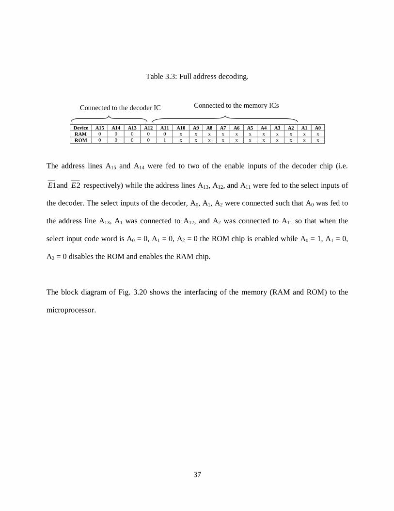
The full address decoding technique was used to generate the chip select signals from the address
bus. This ensures that one and only one memory device was accessed for a given valid address.
It was accomplished by using the 74HCT138 3-line-to-8 line decoder. The most significant bits
of the address lines were used to generate the chip select signals for the memory devices while
the least significant bits were passed on to the memory devices. The address lines A11 to A15
were connected to the decoder IC while A0 to A10 address lines were connected to the memory
ICs. This is shown in Table 3.3.
ROM
RAM
UNUSED
0000H
07FFH
0800H
0FFFH
1000H
FFFFH
37
Table 3.3: Full address decoding.
Device A15 A14 A13 A12 A11 A10 A9 A8 A7 A6 A5 A4 A3 A2 A1 A0
RAM 0 0 0 0 0 x x x x x x x x x x x
ROM 0 0 0 0 1 x x x x x x x x x x x
The address lines A15 and A14 were fed to two of the enable inputs of the decoder chip (i.e.
1E and 2E respectively) while the address lines A13, A12, and A11 were fed to the select inputs of
the decoder. The select inputs of the decoder, A0, A1, A2 were connected such that A0 was fed to
the address line A13, A1 was connected to A12, and A2 was connected to A11 so that when the
select input code word is A0 = 0, A1 = 0, A2 = 0 the ROM chip is enabled while A0 = 1, A1 = 0,
A2 = 0 disables the ROM and enables the RAM chip.
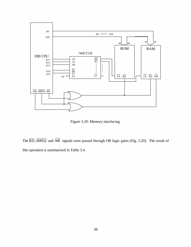
The block diagram of Fig. 3.20 shows the interfacing of the memory (RAM and ROM) to the
microprocessor.
Connected to the decoder IC Connected to the memory ICs
38
Figure 3.20: Memory interfacing.
The RD , MREQ and WR signals were passed through OR logic gates (Fig. 3.20). The result of
this operation is summarized in Table 3.4.
Z80 CPU A11
A12
A13
A14
A15
WR MREQ RD
A2 Y0
A1 Y1
A0
E1
E2
E3 Y7
ROM
CS RD
RAM
CS RD WR
+V
A0 A10
A0
A10
74HCT138
39
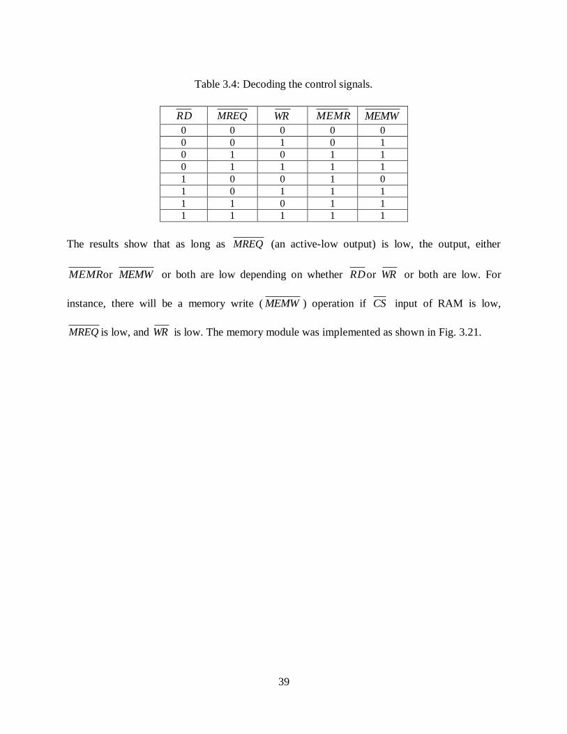
Table 3.4: Decoding the control signals.
RD MREQ WR MEMR MEMW
0 0 0 0 0
0 0 1 0 1
0 1 0 1 1
0 1 1 1 1
1 0 0 1 0
1 0 1 1 1
1 1 0 1 1
1 1 1 1 1
The results show that as long as MREQ (an active-low output) is low, the output, either
MEMRor MEMW or both are low depending on whether RDor WR or both are low. For
instance, there will be a memory write ( MEMW ) operation if CS input of RAM is low,
MREQ is low, and WR is low. The memory module was implemented as shown in Fig. 3.21.
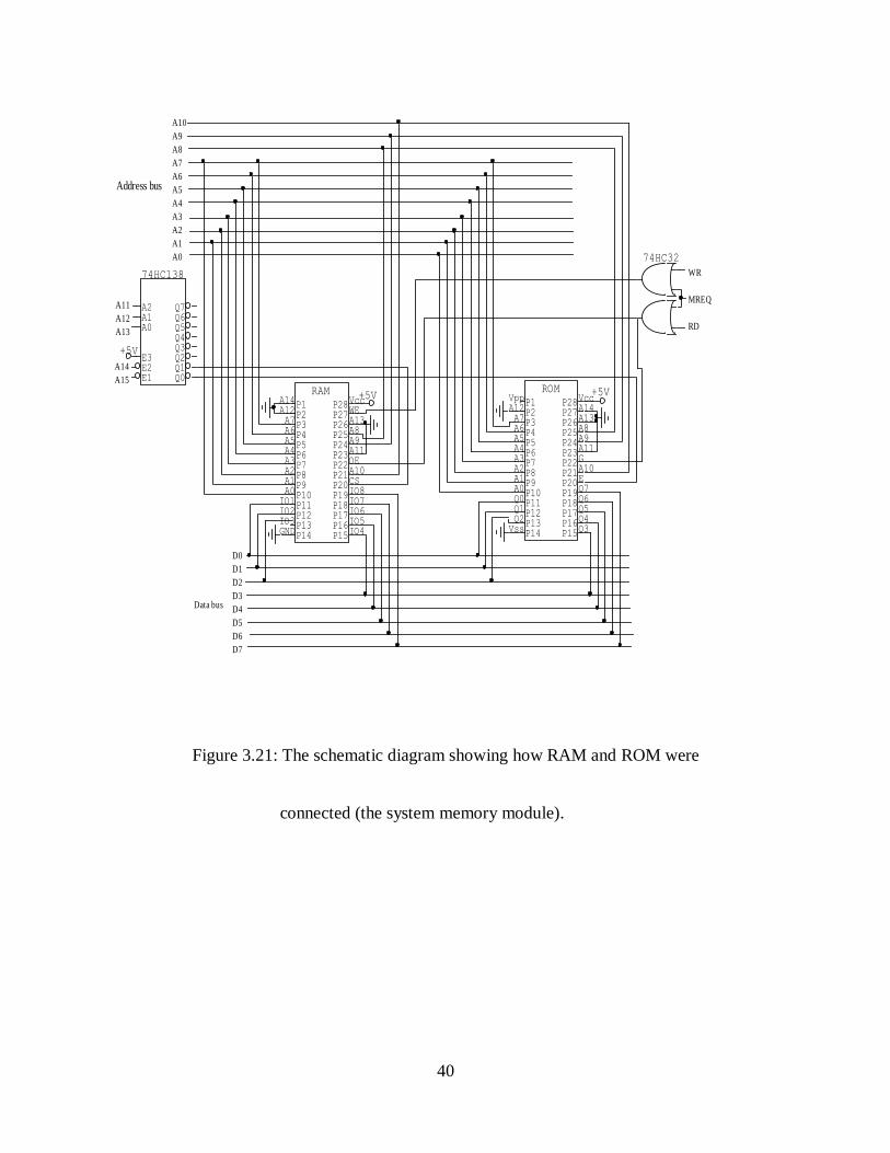
40
A10
A9
A8
A7
A6
A5
A4
A3
A2
A1
A0
Address bus
WR
MREQ
RD
D0
D1
D2
D3
D4
D5
D6
D7
Data bus
A11
A12
A13
A14
A15ROM
VppP1
A12P2A7
P3A6
P4A5
P5A4P6A3
P7A2P8A1
P9A0P10Q0P11Q1P12Q2P13Vss
P14Q3
P15
Q4P16
Q5P17
Q6P18
Q7P19
EP20
A10P21
GP22
A11P23
A9P24
A8P25
A13P26
A14P27
VccP28
RAMA14P1A12
P2A7
P3A6
P4A5
P5A4P6A3
P7A2P8A1
P9A0P10
IO1P11IO2
P12IO3P13GND
P14IO4
P15
IO5P16
IO6P17
IO7P18
IO8P19
CSP20
A10P21
OEP22
A11P23
A9P24
A8P25
A13P26
WEP27
VccP28
A2A1A0
E3E2E1
Q7Q6Q5Q4Q3Q2Q1Q0
74HC138
74HC32
+5V +5V
+5V
Figure 3.21: The schematic diagram showing how RAM and ROM were
connected (the system memory module).

41
3.2 System operating software
The problem was specified as follows: - program to control a motor and relay depending on
sunlight illuminance levels. The algorithm was then developed from which the program
flowchart was obtained. This was then translated into an assembly language program and an
assembler was finally used to generate the machine code program.
3.2.1 The algorithm
The algorithm was developed as follows:
1. Configure port A for input, ports B and C for output
2. Set the stack pointer 0FFFH.
3. Initialize port C such that the motor does nothing and the relay is OFF.
4. Do nothing for approximately 3 sec.
5. Fetch the data at port A.
6. Compare the input data with the night-time code (FFH).
7. If input data = night-time code then go to step 11.
8. Else if input data = day-time code (00H), then go to step 10.
9. Go to step 5.
10.
a. Draw drapes (open) and switch off security lights, wait for 3 seconds, then halt
drape‟s motor.
b. Fetch data at port A.
c. Compare input data with day-time code.

42
d. If input data = day-time code then go to step 10(b).
e. Else if input data = night-time code then go to step 10(f).
f. Draw drapes (close) and switch on security lights, wait for 3 seconds, them halt
drape‟s motor.
g. Wait for 18 seconds.
h. Fetch data at port A.
i. Compare input data with day-time code.
j. If input data = day-time code then go step 10 (l).
k. Else if input data = night-time code then go to step 10 (h).
l. Draw drapes (open) and switch off security lights, wait for 3 seconds, then halt
drape‟s motor.
m. Wait for 18 seconds.
n. Go to step 10 (b).
11.
a. Draw drapes (close) and switch on security lights, wait for 3 seconds, then halt
drape‟s motor.
b. Fetch data at port A.
c. Compare input data with night-time code.
d. If input data = night-time code then go to step 11(b).
e. Else if input data = day-time code then go to step 11(f).
f. Draw drapes (open) and switch off security lights, wait for 3 seconds, then halt
the drape‟s motor.
g. Wait for 18 seconds.
43
h. Fetch data at port A.
i. Compare input data with night-time code.
j. If input data = night-time code then go to step 11(l).
k. Else if input data = day-time code then go to step 11(h).
l. Draw drapes (close) and switch on security lights, wait for 3 seconds, then halt the
drape‟s motor.
m. Wait for 18 seconds.
n. Go to step 11(b).
3.2.2 Program flow chart
The developed algorithm was used to develop the flow chart for the program (Appendix B). A
modular programming approach was adopted and a number of modules/subroutines for
elementary functions were developed. These modules are the day-time subroutine, the night-time
subroutine, and the timer subroutines. The day-time subroutine was decomposed further into
elementary subroutines namely: - OUTDT1, OUTDT2, OUTDT3, and OUTDT4, while the
night-time subroutine was decomposed further into elementary subroutines namely: - OUTNT1,
OUTNT2, OUTNT3, and OUTNT4. Each module was individually tested as a unit and debugged
before all the modules were integrated and tested as the operating software in order to ensure that
the system design met its specifications.
Based on the target application – sunlight illuminance in the morning and in the evening, and to
take care of any power cut to the system, the two subroutines (day-time and night-time) were
necessary. The term „day-time‟ is taken to be the time from 6:30 am to 6:30 pm while the term

44
„night-time‟ is the time from 6:30 pm to 6:30 am. These times were defined from the test results
obtained when investigating the relationship between sunlight illuminance with time of day
(mainly at dawn and dusk). Therefore, when the system is first powered and after the
initialization process, the system then proceeds to either the day-time subroutine or night-time
subroutine depending on the time at which the system is powered.
The OUT subroutine is an initialization process that is designed to cause the drapes motor do
nothing while the lights are switched off upon power-up despite the status of the input signal.
OUTDT1: This is designed to cause the motor turn in the clockwise direction (drapes are drawn
while holding the relay off i.e. security lights are OFF). This is achieved by outputting two
complementary bits to the bidirectional circuit‟s inputs and a logic low to the relay unit‟s input.
The time for which the motor turns is determined by the length that drapes are supposed to cover
and it‟s set by applying a timer subroutine (TIMER1).
OUTDT2: This is meant to cause the motor come to an instant brake while still holding the relay
OFF. It is achieved by outputting two logic high bits to the inputs of the bidirectional circuit and
a logic low bit to the input of the relay unit.
OUTDT3: This is the inverse of OUTDT1. The motor is turned in the anticlockwise (drapes are
drawn) direction and the relay is turned on (security lights are ON). Two complementary bits
(opposite to those in OUTDT1) are output to the bidirectional circuit‟s inputs and a logic high
45
signal is output to the relay unit‟s input. The time for which the motor turns is set by TIMER1
subroutine after which the program goes to OUTDT4.
OUTDT4: This causes the motor to come to an instant brake while maintaining the relay in the
ON position. This is achieved by outputting two logic high bits to the inputs of the bidirectional
switch and a logic high bit to the input of the relay unit.
TIMER1 AND TIMER2 subroutines involve a series of nested subroutines. Three TIMER3
subroutines are nested within the TIMER1 subroutine. Two TIMER4 subroutines are nested
within the TIMER3 subroutine. TIMER4 is designed to provide a 0.5 sec time delay. This is
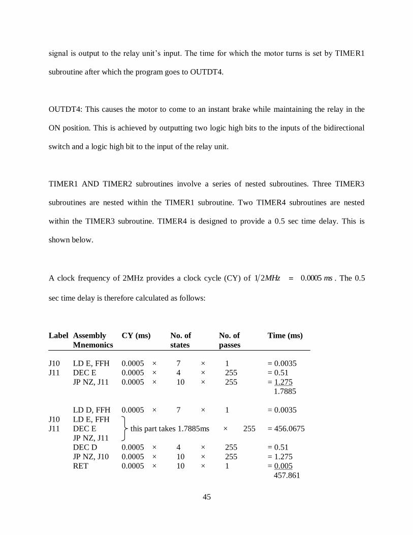
shown below.
A clock frequency of 2MHz provides a clock cycle (CY) of msMHz 0005.021 . The 0.5
sec time delay is therefore calculated as follows:
Label Assembly CY (ms) No. of No. of Time (ms)
Mnemonics states passes
J10 LD E, FFH 0.0005 × 7 × 1 = 0.0035
J11 DEC E 0.0005 × 4 × 255 = 0.51
JP NZ, J11 0.0005 × 10 × 255 = 1.275
1.7885
LD D, FFH 0.0005 × 7 × 1 = 0.0035
J10 LD E, FFH
J11 DEC E this part takes 1.7885ms × 255 = 456.0675
JP NZ, J11
DEC D 0.0005 × 4 × 255 = 0.51
JP NZ, J10 0.0005 × 10 × 255 = 1.275
RET 0.0005 × 10 × 1 = 0.005
457.861
46
Therefore, based on the timing above, TIMER4 subroutine will take approximately 0.5 sec
(457.861ms). Consequently, TIMER3 subroutine which consists of two CALL TIMER4
instructions will take approximately 1 sec (0.5 sec × 2).TIMER1 subroutine provides a 3.0 sec
(1.0 sec x 3) time delay. Six TIMER1 subroutines are nested within the TIMER2 subroutine.
But, TIMER1 provides a 3.0 sec delay, therefore, TIMER2, provides an 18 sec (3.0 sec x 6) time
delay. For demonstration and experimental purposes, TIMER2 was chosen to correspond to the
12 hr time period between either 6:30 am and 6:30 pm or 6:30 pm and 6:30 am. TIMER1 (3.0
sec delay) is the time for which the drape‟s motor turns and it is taken to correspond to the time
that the drapes would take to cover the whole length of, say, a window.
The night-time subroutine also involves a number of elementary subroutines some of which are
similar to or an inverse of those provided in the day-time subroutine. For instance, TIMER1 and
TIMER2 are similar to those presented in the day-time subroutine.
OUTNT1: This causes the motor to turn anticlockwise while causing the relay to turn on. In
other words, the drapes are drawn while the security lights are turned on. It is similar to
OUTDT3.
OUTNT2: This is similar to OUTDT4.
OUTNT3: This causes the motor to turn clockwise and turn off the relay. It‟s the inverse of
OUTNT1.
47
OUTNT4: This is similar to OUTDT2.
3.2.3 Assembly language program and the machine code
A Z80 simulator IDE was used as a development tool to edit, assemble, and debug the system‟s
operating software (Appendix C), prior to downloading into the system‟s UV-EPROM.
The main program starts with an initialization process. Depending on the time of day when the
system has been powered up, the system branches to either the day-time subroutine or the night-
time subroutine as discussed in the foregoing section.
The initialization process involves three steps. The first one is setting up the input/output ports.
The input/output device being used is the 8255 PPI and port A was configured for input while
ports B and C were configured for output. The second step involves setting the stack pointer
(SP). This helps support the subroutine calls. When a subroutine is called the contents of the
program counter (PC) are pushed into the memory location pointed to by the SP and it (SP) is
decremented. When the subroutine has finished executing, the SP is incremented and the
contents of the PC are pushed back from the memory location. In this way, subroutines are
nested to any depth, as long as there is space to push the PC to memory for each call. The final
step in the initialization process involves instructing the microprocessor what to do upon power-
up. This process instructs the system to send a logic low signal to the logic inputs of the output
devices so that they are held stopped. Then the microprocessor samples the data at the input port
48
so as to establish whether it is day-time or night-time and hence branch to the appropriate
subroutine.
3.3 System troubleshooting
The idea was to develop a simple program and make the processor step through one machine
cycle at a time. This made it possible to use a logic probe to examine the contents of the system
bus lines as the microprocessor was being single-stepped. To single-step the microprocessor, a
single-step circuit was built (Fig. 3.22). This circuit utilizes the built-in wait capability of the Z80
microprocessor. In the WAIT state the microprocessor “idles”, holding valid addresses, control
signals, and data on its buses. The WAIT input line of the Z80 microprocessor is sampled with
the falling edge of the clock signal during the T2 clock period of each machine cycle. If WAIT is
LOW the processor enters a WAIT state with valid addresses, control signals, and data on its
buses. This WAIT state persists indefinitely until the WAIT input is found high on the falling
edge of the clock. At this time, the program execution continues normally with the T3 state of
the current machine cycle.
The test program thus developed was: A program to check the status of the 8 bits at Port A and
output AAH to Port C if the 8 bits are logic low and 55H if they are all logic high. The program
list is provided in Table 3.5.
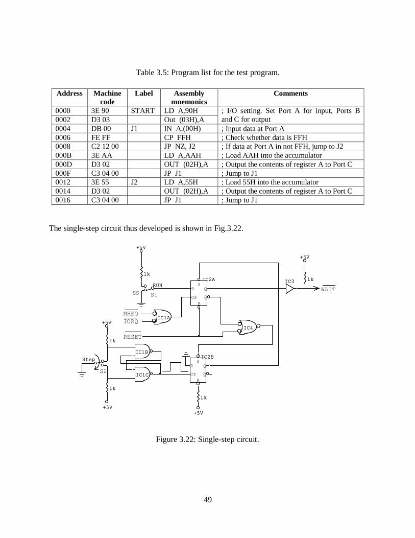
49
Table 3.5: Program list for the test program.
Address Machine
code
Label Assembly
mnemonics
Comments
0000 3E 90 START LD A,90H ; I/O setting. Set Port A for input, Ports B
and C for output 0002 D3 03 Out (03H),A
0004 DB 00 J1 IN A,(00H) ; Input data at Port A
0006 FE FF CP FFH ; Check whether data is FFH
0008 C2 12 00 JP NZ, J2 ; If data at Port A in not FFH, jump to J2
000B 3E AA LD A,AAH ; Load AAH into the accumulator
000D D3 02 OUT (02H),A ; Output the contents of register A to Port C
000F C3 04 00 JP J1 ; Jump to J1
0012 3E 55 J2 LD A,55H ; Load 55H into the accumulator
0014 D3 02 OUT (02H),A ; Output the contents of register A to Port C
0016 C3 04 00 JP J1 ; Jump to J1
The single-step circuit thus developed is shown in Fig.3.22.
SSWAIT
S2
S1
MREQ
IORQ
RESET
+5V
IC3
+5V
+5V
Step
IC1C
IC1B
+5V
IC4
IC1A
SD
CP
R
Q_Q
IC2B
SD
CP
R
Q_Q
IC2A
RUN
+5V
1k
1k
1k
1k
1k
+5V
IC3
+5V
+5V
Step
IC1C
IC1B
+5V
IC4
IC1A
SD
CP
R
Q_Q
IC2B
SD
CP
R
Q_Q
IC2A
RUN
+5V
1k
1k
1k
1k
1k
Figure 3.22: Single-step circuit.

50
The operation of this circuit is as follows:
i. When power is first applied or when the reset switch is pushed, IC2A is reset and IC2B is
set.
ii. With switch S1 in the RUN position, any I/O or memory request will set flip-flop IC2A
and cause the WAIT line to go high. The processor will run normally.
iii. When S1 is pushed to the single-step position, any I/O or memory request will reset IC2A
and cause WAIT to go low. This will in turn cause the Z80 microprocessor to enter a
WAIT state as soon as T2 of the next machine cycle occurs.
iv. Pushing the STEP switch now resets IC2B, sets IC2A, and forces WAIT high. The Q
output of IC2A also sets IC2B, and this allows the next I/O or memory request to again
clock the WAIT line low. The effect is to execute one machine cycle each time the STEP
switch is pushed.
By monitoring the IORQ or WR control bus signal, the M3 cycles of the OUT instructions were
found and the contents of each of the buses were then examined by use of a logic probe.
51
CHAPTER FOUR
RESULTS AND DISCUSSION
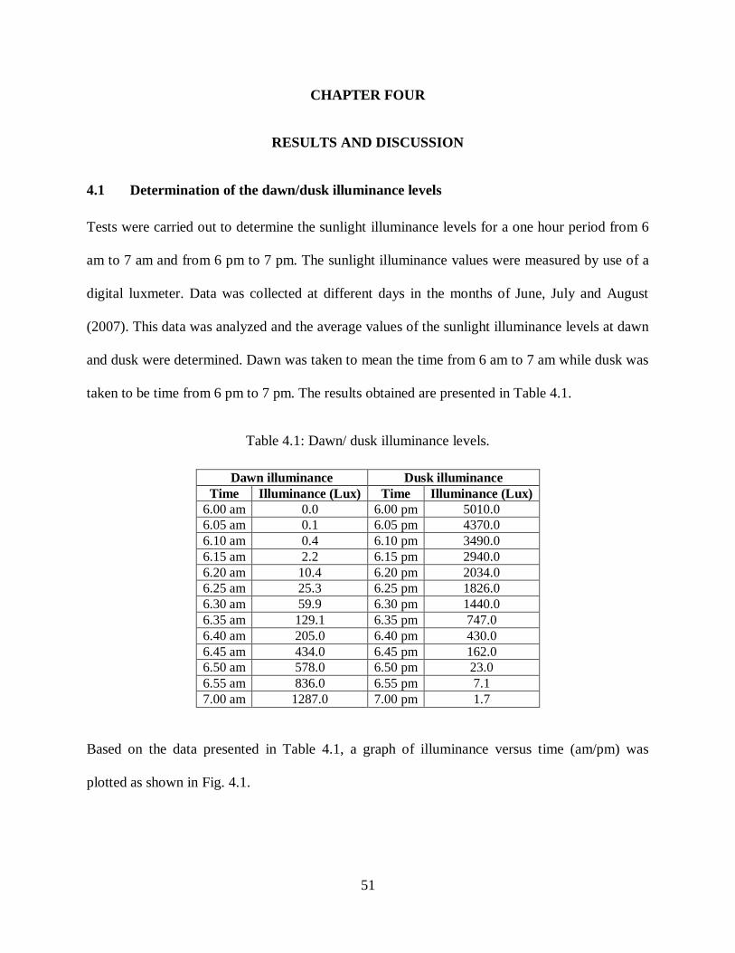
4.1 Determination of the dawn/dusk illuminance levels
Tests were carried out to determine the sunlight illuminance levels for a one hour period from 6
am to 7 am and from 6 pm to 7 pm. The sunlight illuminance values were measured by use of a
digital luxmeter. Data was collected at different days in the months of June, July and August
(2007). This data was analyzed and the average values of the sunlight illuminance levels at dawn
and dusk were determined. Dawn was taken to mean the time from 6 am to 7 am while dusk was
taken to be time from 6 pm to 7 pm. The results obtained are presented in Table 4.1.
Table 4.1: Dawn/ dusk illuminance levels.
Dawn illuminance Dusk illuminance
Time Illuminance (Lux) Time Illuminance (Lux)
6.00 am 0.0 6.00 pm 5010.0
6.05 am 0.1 6.05 pm 4370.0
6.10 am 0.4 6.10 pm 3490.0
6.15 am 2.2 6.15 pm 2940.0
6.20 am 10.4 6.20 pm 2034.0
6.25 am 25.3 6.25 pm 1826.0
6.30 am 59.9 6.30 pm 1440.0
6.35 am 129.1 6.35 pm 747.0
6.40 am 205.0 6.40 pm 430.0
6.45 am 434.0 6.45 pm 162.0
6.50 am 578.0 6.50 pm 23.0
6.55 am 836.0 6.55 pm 7.1
7.00 am 1287.0 7.00 pm 1.7
Based on the data presented in Table 4.1, a graph of illuminance versus time (am/pm) was
plotted as shown in Fig. 4.1.
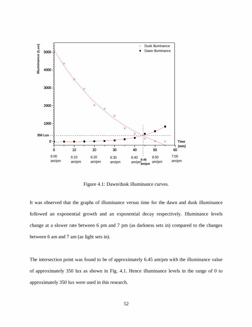
52
0 10 20 30 40 50 60
0
1000
2000
3000
4000
5000
0 10 20 30 40 50 60
0
1000
2000
3000
4000
5000
Dusk illuminance
Time
(min)
Illu
min
an
ce
(L
ux
)
Dawn illuminance
6:00
am/pm6:10
am/pm
6:20
am/pm6:30
am/pm
6:40
am/pm6:45
am/pm
6:50
am/pm
7:00
am/pm
350 Lux
Figure 4.1: Dawn/dusk illuminance curves.
It was observed that the graphs of illuminance versus time for the dawn and dusk illuminance
followed an exponential growth and an exponential decay respectively. Illuminance levels
change at a slower rate between 6 pm and 7 pm (as darkness sets in) compared to the changes
between 6 am and 7 am (as light sets in).
The intersection point was found to be of approximately 6.45 am/pm with the illuminance value
of approximately 350 lux as shown in Fig. 4.1. Hence illuminance levels in the range of 0 to
approximately 350 lux were used in this research.
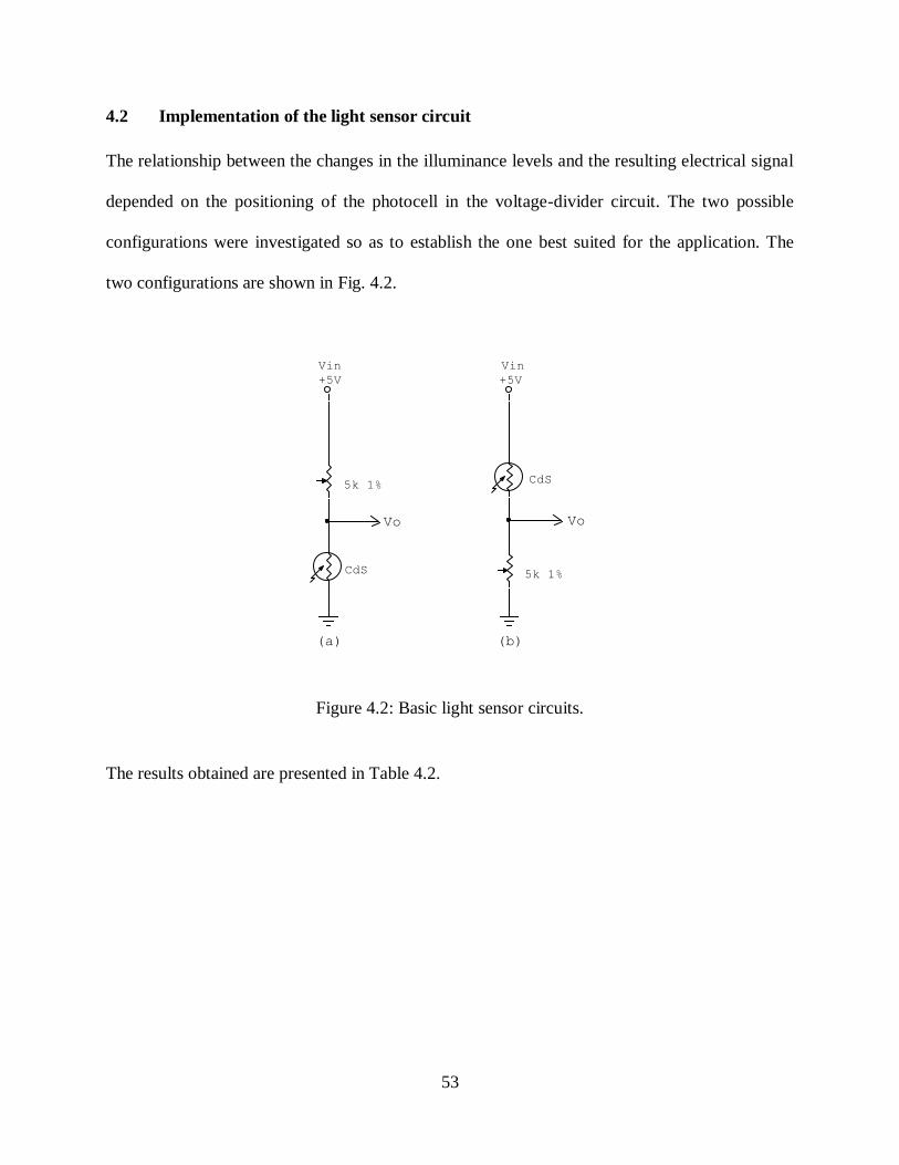
53
4.2 Implementation of the light sensor circuit
The relationship between the changes in the illuminance levels and the resulting electrical signal
depended on the positioning of the photocell in the voltage-divider circuit. The two possible
configurations were investigated so as to establish the one best suited for the application. The
two configurations are shown in Fig. 4.2.
VoVo
(b)(a)
Vin
+5V
Vin
+5V
5k 1%
5k 1%CdS
CdS
Figure 4.2: Basic light sensor circuits.
The results obtained are presented in Table 4.2.

54
Table 4.2: Implementation of the photocell.
Illuminance (Lux)
Average Vo (V)
Fig. 4.2(a) Fig. 4.2(b)
280 1.17 4.68
260 1.21 4.80
240 1.26 4.71
220 1.31 4.63
200 1.36 4.56
180 1.42 4.46
160 1.49 4.36
140 1.58 4.24
120 1.72 4.11
100 1.86 3.93
80 2.05 3.70
60 2.32 3.44
40 2.67 3.00
20 3.36 2.17
0 5.73 0.39
The results were then analyzed in a graph of illuminance versus output voltage as shown in Fig.
4.3.
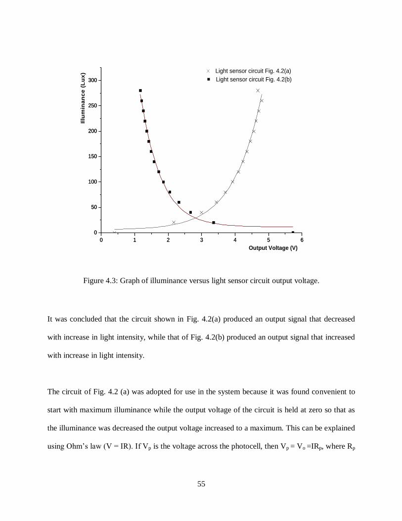
55
0 1 2 3 4 5 6
0
50
100
150
200
250
300
0 1 2 3 4 5 6
0
50
100
150
200
250
300Il
lum
ina
nc
e (
Lu
x)
Output Voltage (V)
Light sensor circuit Fig. 4.2(a)
Light sensor circuit Fig. 4.2(b)
Figure 4.3: Graph of illuminance versus light sensor circuit output voltage.
It was concluded that the circuit shown in Fig. 4.2(a) produced an output signal that decreased
with increase in light intensity, while that of Fig. 4.2(b) produced an output signal that increased
with increase in light intensity.
The circuit of Fig. 4.2 (a) was adopted for use in the system because it was found convenient to
start with maximum illuminance while the output voltage of the circuit is held at zero so that as
the illuminance was decreased the output voltage increased to a maximum. This can be explained
using Ohm‟s law (V = IR). If Vp is the voltage across the photocell, then Vp = Vo =IRp, where Rp
56
is the resistance of the photocell. Since the resistance of the photocell increases with a decrease
in the illuminance, then the output voltage Vo is going to increase as well.
4.3 Analogue signal amplification
The results of the analogue signal amplification are presented in Table 4.3.
Table 4.3: Analogue signal amplification.
Illuminance(Lux)
Analogue input voltage
Vin(V)
Amplified analogue output
voltage Vout(V)
340 0.287 0.70
320 0.303 0.74
300 0.321 0.78
280 0.339 0.81
260 0.357 0.86
240 0.376 0.90
220 0.395 0.94
200 0.424 1.00
180 0.464 1.08
160 0.511 1.19
140 0.571 1.31
120 0.614 1.40
100 0.720 1.61
80 0.848 1.88
60 1.052 2.30
40 1.330 2.86
20 1.805 3.84
10 2.214 4.66
0 3.350 4.96
The AD623 is designed to offer accurate gains using 0.1% - 1% tolerance resistors. A gain
resistor RG = 100 kΩ and with a tolerance value of 1% was used. This yielded a gain of 2 as
shown below.

57
2
1100
100
1100
G
k
kG
R
kG
G
The percent error in the gain of the amplified analogue electrical signal was then determined.
This was important so as to establish how the gain obtained in the amplified signal varied from
the expected gain (G = 2) as set by resistor RG. The results are presented in Table 4.4.
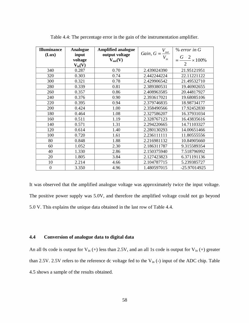
58
Table 4.4: The percentage error in the gain of the instrumentation amplifier.
Illuminance
(Lux)
Analogue
input
voltage
Vin(V)
Amplified analogue
output voltage
Vout(V) in
out
V
VGGain,
%1002
2
%
G
Ginerror
340 0.287 0.70 2.439024390 21.95121951
320 0.303 0.74 2.442244224 22.11221122
300 0.321 0.78 2.429906542 21.49532710
280 0.339 0.81 2.389380531 19.46902655
260 0.357 0.86 2.408963585 20.44817927
240 0.376 0.90 2.393617021 19.68085106
220 0.395 0.94 2.379746835 18.98734177
200 0.424 1.00 2.358490566 17.92452830
180 0.464 1.08 2.327586207 16.37931034
160 0.511 1.19 2.328767123 16.43835616
140 0.571 1.31 2.294220665 14.71103327
120 0.614 1.40 2.280130293 14.00651466
100 0.720 1.61 2.236111111 11.80555556
80 0.848 1.88 2.216981132 10.84905660
60 1.052 2.30 2.186311787 9.315589354
40 1.330 2.86 2.150375940 7.518796992
20 1.805 3.84 2.127423823 6.371191136
10 2.214 4.66 2.104787715 5.239385727
0 3.350 4.96 1.480597015 -25.97014925
It was observed that the amplified analogue voltage was approximately twice the input voltage.
The positive power supply was 5.0V, and therefore the amplified voltage could not go beyond
5.0 V. This explains the unique data obtained in the last row of Table 4.4.
4.4 Conversion of analogue data to digital data
An all 0s code is output for Vin (+) less than 2.5V, and an all 1s code is output for Vin (+) greater
than 2.5V. 2.5V refers to the reference dc voltage fed to the Vin (-) input of the ADC chip. Table
4.5 shows a sample of the results obtained.
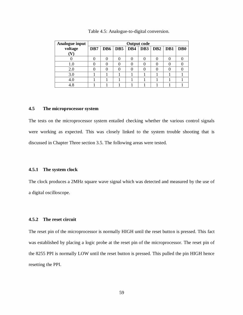
59
Table 4.5: Analogue-to-digital conversion.
Analogue input
voltage
(V)
Output code
DB7 DB6 DB5 DB4 DB3 DB2 DB1 DB0
0 0 0 0 0 0 0 0 0
1.0 0 0 0 0 0 0 0 0
2.0 0 0 0 0 0 0 0 0
3.0 1 1 1 1 1 1 1 1
4.0 1 1 1 1 1 1 1 1
4.8 1 1 1 1 1 1 1 1
4.5 The microprocessor system
The tests on the microprocessor system entailed checking whether the various control signals
were working as expected. This was closely linked to the system trouble shooting that is
discussed in Chapter Three section 3.5. The following areas were tested.
4.5.1 The system clock
The clock produces a 2MHz square wave signal which was detected and measured by the use of
a digital oscilloscope.
4.5.2 The reset circuit
The reset pin of the microprocessor is normally HIGH until the reset button is pressed. This fact
was established by placing a logic probe at the reset pin of the microprocessor. The reset pin of
the 8255 PPI is normally LOW until the reset button is pressed. This pulled the pin HIGH hence
resetting the PPI.

60
The actions of the reset circuit were investigated using a digital oscilloscope and the results are
summarized in Fig. 4.4.
Figure 4.4: Operations of the reset circuit.
With the RC network connected to the reset input, the capacitor holds the reset pin low for
several time constants when power is first applied. Because the reset signal obtained across the
capacitor is a rising exponential and not a sharp square wave (Fig. 4.4 (a)), the Schmitt trigger is
used to square the wave shape. The first 74HC14 Schmitt trigger switches to the low-level
output when its input exceeds 2.0V while the next Schmitt trigger switches to a high-level output
(Fig. 4.4(b)). The input to the first Schmitt trigger then has to go below 1.7V before the output
switches back to logic 1. That is, the logic 1 and logic 0 switching points are not the same.
Resetting the circuit gives a logic low output at the circuit output.
Vc
2.0V
(a) Node A (b) Node B (c) Upon reset
Vc = voltage across the capacitor
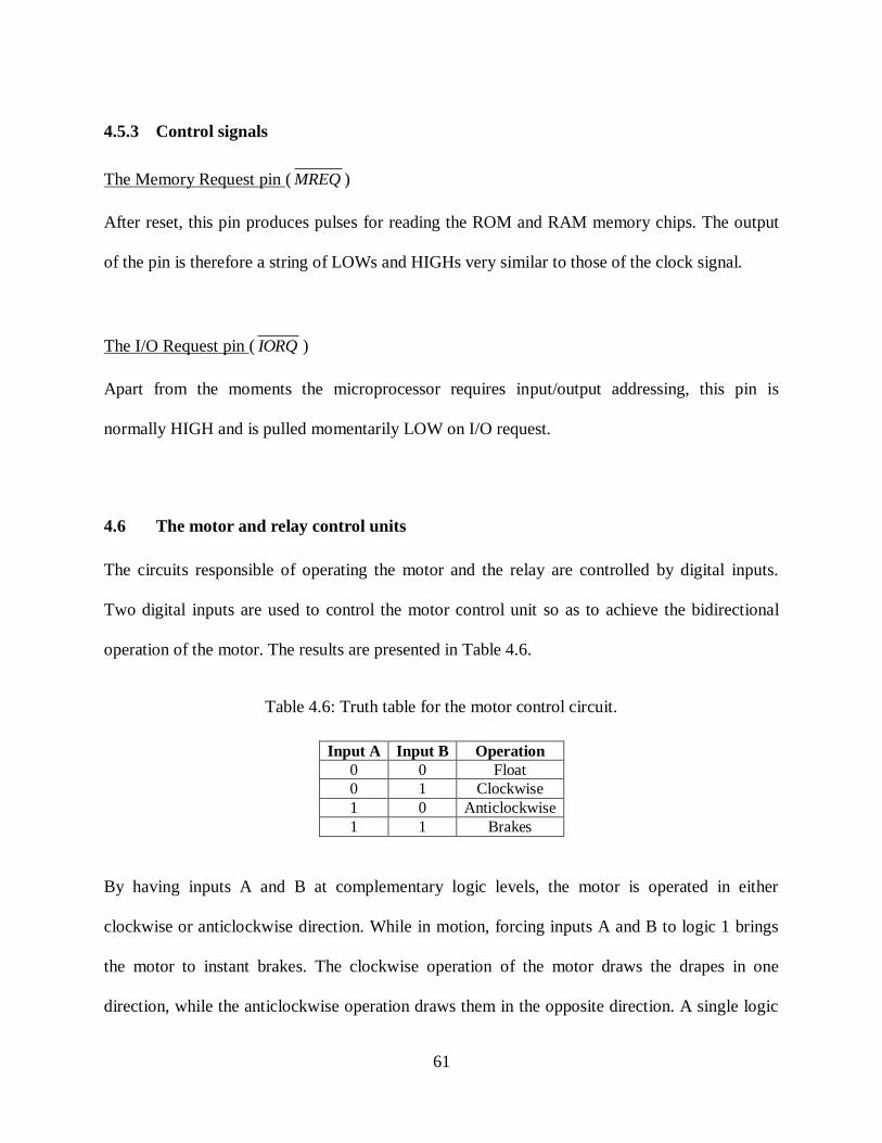
61
4.5.3 Control signals
The Memory Request pin ( MREQ )
After reset, this pin produces pulses for reading the ROM and RAM memory chips. The output
of the pin is therefore a string of LOWs and HIGHs very similar to those of the clock signal.
The I/O Request pin ( IORQ )
Apart from the moments the microprocessor requires input/output addressing, this pin is
normally HIGH and is pulled momentarily LOW on I/O request.
4.6 The motor and relay control units
The circuits responsible of operating the motor and the relay are controlled by digital inputs.
Two digital inputs are used to control the motor control unit so as to achieve the bidirectional
operation of the motor. The results are presented in Table 4.6.
Table 4.6: Truth table for the motor control circuit.
Input A Input B Operation
0 0 Float
0 1 Clockwise
1 0 Anticlockwise
1 1 Brakes
By having inputs A and B at complementary logic levels, the motor is operated in either
clockwise or anticlockwise direction. While in motion, forcing inputs A and B to logic 1 brings
the motor to instant brakes. The clockwise operation of the motor draws the drapes in one
direction, while the anticlockwise operation draws them in the opposite direction. A single logic

62
input is used to control the relay unit such that logic 1 input forces open the normally closed
contact of the relay. This closes the ac load circuit hence lighting the ac lamp. The inverse
happens with a logic 0 input.

63
CHAPTER FIVE
CONCLUSION AND RECOMMENDATIONS
5.1 Conclusion
By using CMOS logic and an 8-bit microprocessor, a low cost automatic light- and time-based
control system for drapes and security lights has been developed. The system serves as a basis
upon which complex systems using either 16- or 32-bit microprocessors can be developed.
There is total agreement between the system designed and the required operation of the system.
For this reason, the system can be employed in homes and in any other setup where manned
security is not mandatory. It can also be applied in such places as institutions and commercial
premises despite the presence of security personnel.
5.2 Recommendations
For improving on the system and making it more effective, various suggestions should be
considered for further work.
The system can be upgraded by use of a 16- or 32-bit microprocessor for speed optimization and
greater functionality. Full utilization of the system can be achieved by incorporating more
sensors to make use of the microprocessor‟s large instruction set and the unused port of the I/O
chip. The 8255 PIO can also be replaced with a Z80 PIO so as to make use of the Z80 PIO‟s

64
superior interrupt handling capability and accommodate increased utilization of the system
through the incorporation of additional sensors.
65
REFERENCES
Anderson, S. (1997). Microprocessor Technology. Butterworth-Heinemann Ltd, Jordan Hill,
Oxford, pp. 34 – 206, pp. 265-267, pp. 297 – 320.
Bierman, A. (2003). Photosensor and Control System for Dimming Lighting Fixtures to Reduce
Power Consumption, United States Patent, Patent No. US 6,583,573 B2.
Cheek, P., Linda, N. and Heather, D. (2005). Aging Well with Smart Technology, Nurs
Administration, Volume 29, Issue 4, pp. 329 – 338.
Clements, A. (2000). The Principles of Computer Hardware. Third edition. Oxford University
Press, New York. Pp. 461 – 478, pp. 642 – 655.
D‟Olima, O. (2005). Portable Water Scanner, http://www.ece.ncsu.edu/seniordesign/course_
documents.
Dewsbury, G., Clarke, K., Hughes, J., Rouncefield, M. and Sommerville, I. (2003). Growing
Older Digitally: Designing Technology for Older People, In Proceedings of INCLUDE 2003,
inclusive design society and business, Helen Hamlyn Research Center, Royal College of Art (25
–28 March 2003), pp. 57 – 64.
66
Dewsbury, G., Clarke, K., Hughes, J., Rouncefield, M., Sommerville, I., Taylor, B. and Edge, M.
(2003). Designing Acceptable „Smart‟ Home Technology to Support People in the Home,
Technology and Disability, Volume 15, pp. 191 – 199.
Dharmawan, H. A. and Ali, S. A. M. (2001/2002). Design of switchable transformer control
system employing the microcontroller 80C552, International Journal of Applied
Electromagnetics and Mechanics, Volume 13, pp. 99 – 106.
Erhlich, C., Papamichael, K., Lai, J. and Revzan, K. (2001). A Method for Simulating the
Performance of Photosensor-based Lighting Controls, Energy and Building, Volume 6, pp. 438 –
446.
Floyd, T. L. (2003). Digital Fundamentals. Eighth edition. Pearson Education, New Jersey. Pp.
616 – 750.
Ganssle, J. (1997). The Art of Programming Embedded Systems. Academic Press Publishers,
New Jersey. Pp. 11 – 99, pp. 63 – 73.
Garrod, S. A. R. and Borns, R. J. (1991). Digital Logic: Analysis, Application and Design.
Saunders College Publishing, Orlando, Florida. Pp. 477 – 479, pp. 739 – 759, pp. 778 – 789, pp.
794 – 796, pp. 888 – 927.
67
Gonzalez, O., Rodriguez, M., Ayala, A., Hernandez, J., and Rodriguez, S., (2004). Application
of PICs and Microcontrollers in the measurement and control of parameters in industry,
International Journal of Electrical Engineering Education, Volume 41, Issue 3, pp. 265 – 274.
Hai, (2007), http://www.homeauto.com, 14-10-2007.
Hall, D. V. (1992). Microprocessors and Interfacing: Programming and Hardware. Tata
McGraw-Hill, New Delhi. Pp. 261 – 357.
Hanley, T. (1993). Microprocessors and Microcomputer Technology. DP Publications, London,
pp. 199 – 216, pp.223 – 248, pp. 255 – 293, pp. 314 – 329.
Hayes, J. P. (1998). Computer Architecture and Organization. Third edition. McGraw-Hill,
Singapore, pp. 64 – 126.
Home Automation, http://en.wikipedia.org/wiki/homeautomation, 14-10-2007.
Jain, R. P. (2003). Modern Digital Electronics. Third Edition. Tata McGraw-Hill, New Delhi,
pp. 213 – 370.
Langsdorf, M., Rall, M., Schuchman, D. and Rinehart, P. (1997). Temperature Control of a
Microscope Drier, Conference Proceedings: National Conference on Undergraduate Research,
Austin TX, pp. 52 – 67.
68
Malvino, A. P. and Brown, J. A. (2006). Digital Computer Electronics. Third edition. Tata
McGraw-Hill, Singapore, pp. 64 – 126.
Mano, M. M. and Kime, C. R. (2005). Logic and Computer Design Fundamentals. Second
edition. Pearson Education, New Delhi, pp. 511 – 609.
McDonald, J. (1997). Temperature Control Using a Microcontroller: An Interdisciplinary
Engineering Design Project, National Conference on Undergraduate Research, Austin TX, pp. 38
– 46.
Microchip (2004), Microcontrollers, http://www.ece.ncsu.edu, 25-09-2006.
Otieno, F. O., Kola, B. O. and Onyango, F. N. (1997). On-line determination of thermophysical
properties in an absorption calorimeter, Measurement Science Technology, Volume 8, pp. 239 –
244.
Paton, J. D. (2007), Daylight Control System Device and Method, United States Patent, Patent
No. US 7,190,126 B1.
Pitigoi-Aron, R., Forke U., Viala R. (2007), Diode-based Light Sensors and Methods, United
States Patent, Patent No. US 7,164,110 B2.
69
Popat, P. P. (2000), Closed-loop, Daylight-Sensing, Automatic Window-Covering System
Insensitive to Radiant Spectrum Produced by Gaseous Discharge Lamps, United States Patent,
Patent No. US 6,084,231.
Rubinstein, F., Ward, G. and Verderber, R. (1989). Improving the Performance of Photo-
Electrically Controlled Lighting Systems, Journal of the IESNA, Volume 18, Issue 1, pp. 70 –
94.
Shoewu, O. and Baruwa, O. T. (2006). Design of a Microprocessor-based Automatic Gate, The
Pacific Journal of Science and Technology, Volume 7, Issue 1, pp. 31 – 44.
Soja, R. (2002). MCU Applications, Electronic News (North America), Volume 48, Issue 38, pp.
61 – 66.
Sunybroome Educational (2006), Microcontrollers and Microprocessors,
http://www.sunybroome.edu, 25-09-2006.
Uddin, M. R., Gazi, M. and Shahidul, I. (2005). Microcontroller-based Light Control,
International Journal of Software Engineering and Knowledge Engineering; April 2005, Volume
15, Issue 2, pp. 319 – 324.
Uffenbeck, J. (2000). Microcomputers and Microprocessors: The 8080, 8085, and Z80
Programming, Interfacing and Troubleshooting. Third edition. Prentice Hall, New Jersey. P. 5,

70
pp. 31 – 38, pp. 49 – 80, pp. 150 – 159, pp. 177 – 187, pp. 201 – 206, pp. 229 – 255, pp. 568 –
608.
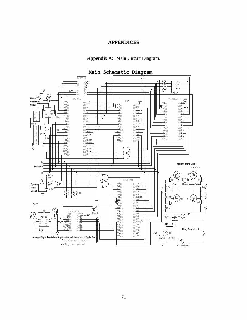
71
APPENDICES
Appendix A: Main Circuit Diagram.
Main Schematic Diagram
Motor Control Unit
2N4401
Relay Control Unit
Analogue Signal Acquisition, Amplification, and Conversion to Digital Data
Analogue ground
Digital ground
8MHz
Clock
Generator
Circuit
2MHz
Do
D7
Data bus
System
Reset
Circuit
A
B
10k
10k
10k
10k
10k
250
24k
CdS
100k
10k
5.6k
17k
47 47
3.3k 3.3k
10k 10k
470 470
SD
CP
R
Q_Q
SD
CP
R
Q_Q
8MHz Xtal Mod
8255 PPI
PA3P1PA2P2PA1P3PA0P4RDP5CSP6
GNDP7A1P8A0
P9PC7
P10PC6
P11PC5P12PC4P13PC0P14PC1P15PC2P16PC3P17PB0
P18PB1P19PB2
P20PB3
P21
PB4P22
PB5P23
PB6P24
PB7P25
VccP26
D7P27
D6P28
D5P29
D4P30
D3P31
D2P32
D1P33
D0P34
RESETP35
WRP36
PA7P37
PA6P38
PA5P39
PA4P40
UV-EPROM
VppP1
A12P2
A7P3
A6P4
A5P5
A4P6A3P7A2
P8A1
P9A0
P10
D0P11D1P12
D2P13
VssP14 D3P15
D4P16
D5P17
D6P18
D7P19
EP20
A10P21
GP22
A11P23
A9P24
A8P25
A13P26
A14P27
VccP28
SRAM
A14P1
A12P2A7
P3A6P4A5P5A4
P6A3
P7A2P8
A1P9
A0P10
IO1P11IO2
P12IO3P13GND
P14IO4
P15
IO5P16
IO6P17
IO7P18
IO8P19
CSP20
A10P21
OEP22
A11P23
A9P24
A8P25
A13P26
WEP27
VccP28
Z80 CPU
A11P1A12
P2A13P3A14
P4A15P5CLKP6D4
P7D3
P8D5
P9D6
P10VccP11
D2P12D7
P13D0P14D1
P15INTP16NMIP17HALT
P18MREQ
P19IORQ
P20RD
P21
WRP22
BUSAKP23
WAITP24
BUSRQP25
RESETP26
M1P27
RFSHP28
GNDP29
A0P30
A1P31
A2P32
A3P33
A4P34
A5P35
A6P36
A7P37
A8P38
A9P39
A10P40
+5V+5V
A2A1A0
E3E2E1
Q7Q6Q5Q4Q3Q2Q1Q0
74HC138
+5V
+5V
+5V
+5V
74HC14
4.7uF
S2
+5V
+5V
+5V
0.1uF
+10uF
IN+IN- V+
V-OUTREF
RGRG
AD620
S
150pF
+10uF
ADC0804CSP1RD
P2WRP3
CLKRP4INT
P5 VpluP6 VmnuP7A GNDP8VrefP9D GNDP10 D0P11
D1P12
D2P13
D3P14
D4P15
D5P16
D6P17
D7P18
CLKINP19
VccP20
ac source
240V
+12V
Q9
12VSPDT
+12V
Q3 Q4
Q1Q2
Q5
Q6 Q7
Q8
Motor
+5V
+5V
10k
10k
10k
10k
10k
250
24k
CdS
100k
10k
5.6k
17k
47 47
3.3k 3.3k
10k 10k
470 470
SD
CP
R
Q_Q
SD
CP
R
Q_Q
8MHz Xtal Mod
8255 PPI
PA3P1PA2P2PA1P3PA0P4RDP5CSP6
GNDP7A1P8A0
P9PC7
P10PC6
P11PC5P12PC4P13PC0P14PC1P15PC2P16PC3P17PB0
P18PB1P19PB2
P20PB3
P21
PB4P22
PB5P23
PB6P24
PB7P25
VccP26
D7P27
D6P28
D5P29
D4P30
D3P31
D2P32
D1P33
D0P34
RESETP35
WRP36
PA7P37
PA6P38
PA5P39
PA4P40
UV-EPROM
VppP1
A12P2
A7P3
A6P4
A5P5
A4P6A3P7A2
P8A1
P9A0
P10
D0P11D1P12
D2P13
VssP14 D3P15
D4P16
D5P17
D6P18
D7P19
EP20
A10P21
GP22
A11P23
A9P24
A8P25
A13P26
A14P27
VccP28
SRAM
A14P1
A12P2A7
P3A6P4A5P5A4
P6A3
P7A2P8
A1P9
A0P10
IO1P11IO2
P12IO3P13GND
P14IO4
P15
IO5P16
IO6P17
IO7P18
IO8P19
CSP20
A10P21
OEP22
A11P23
A9P24
A8P25
A13P26
WEP27
VccP28
Z80 CPU
A11P1A12
P2A13P3A14
P4A15P5CLKP6D4
P7D3
P8D5
P9D6
P10VccP11
D2P12D7
P13D0P14D1
P15INTP16NMIP17HALT
P18MREQ
P19IORQ
P20RD
P21
WRP22
BUSAKP23
WAITP24
BUSRQP25
RESETP26
M1P27
RFSHP28
GNDP29
A0P30
A1P31
A2P32
A3P33
A4P34
A5P35
A6P36
A7P37
A8P38
A9P39
A10P40
+5V+5V
A2A1A0
E3E2E1
Q7Q6Q5Q4Q3Q2Q1Q0
74HC138
+5V
+5V
+5V
+5V
74HC14
4.7uF
S2
+5V
+5V
+5V
0.1uF
+10uF
IN+IN- V+
V-OUTREF
RGRG
AD620
S
150pF
+10uF
ADC0804CSP1RD
P2WRP3
CLKRP4INT
P5 VpluP6 VmnuP7A GNDP8VrefP9D GNDP10 D0P11
D1P12
D2P13
D3P14
D4P15
D5P16
D6P17
D7P18
CLKINP19
VccP20
ac source
240V
+12V
Q9
12VSPDT
+12V
Q3 Q4
Q1Q2
Q5
Q6 Q7
Q8
Motor
+5V
+5V
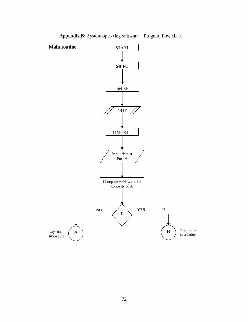
72
START
Set I/O
Set SP
OUT
TIMER1
0?
Input data at
Port A
Compare FFH with the
contents of A
A B
NO YES
Day-time
subroutine
Night-time
subroutine
Main routine
J3
Appendix B: System operating software – Program flow chart.

73
TIMER1
Input data at Port A
Compare 00H with the contents of A
0?
0?
A
OUTDT1
OUTDT2
OUTDT3
TIMER1
OUTDT4
TIMER2
Input data at Port A
Compare 00H with the contents of A
OUTDT1
TIMER1
OUTDT2
TIMER2
NOP
NOP
NOP
NOP
NOP
NOP
J1 J1
J6
J2
J7
Day-time subroutine
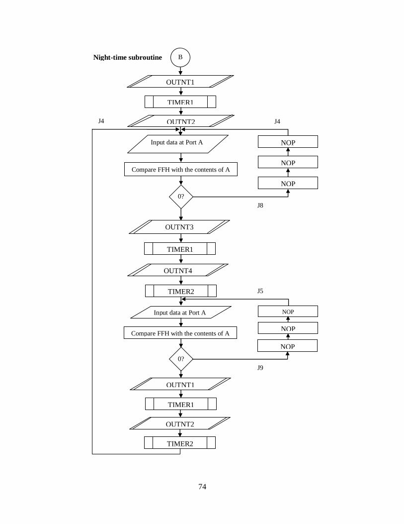
74
TIMER1
Input data at Port A
Compare FFH with the contents of A
0?
0?
B
OUTNT1
OUTNT2
OUTNT3
TIMER1
OUTNT4
TIMER2
Input data at Port A
Compare FFH with the contents of A
OUTNT1
TIMER1
OUTNT2
TIMER2
NOP
NOP
NOP
NOP
NOP
NOP
J5
J8
J9
J4 J4
Night-time subroutine
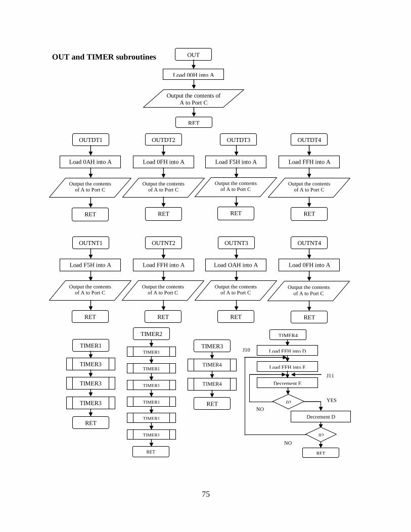
75
OUT
OUTDT1
RET
OUTDT4
OUTDT3
Load 00H into A
Output the contents of
A to Port C
OUTDT2
Load 0AH into A Load 0FH into A Load F5H into A Load FFH into A
Output the contents of A to Port C
RET
Output the contents of A to Port C
RET
Output the contents of A to Port C
RET
Output the contents of A to Port C
RET
OUTNT1
OUTNT2
OUTNT3
OUTNT4
Load F5H into A Load FFH into A Load OAH into A Load 0FH into A
Output the contents of A to Port C
Output the contents of A to Port C
Output the contents of A to Port C
Output the contents
of A to Port C
RET RET RET RET
TIMER1
TIMER3
TIMER3
TIMER3
RET
TIMER2
TIMER1
TIMER1
TIMER1
TIMER1
TIMER1
TIMER1
TIMER3
TIMER4
TIMER4
RET
TIMER4
0?
Load FFH into D
Load FFH into E
Decrement E
Decrement D
0?
NO
YES
NO
J10
J11
RET RET
OUT and TIMER subroutines
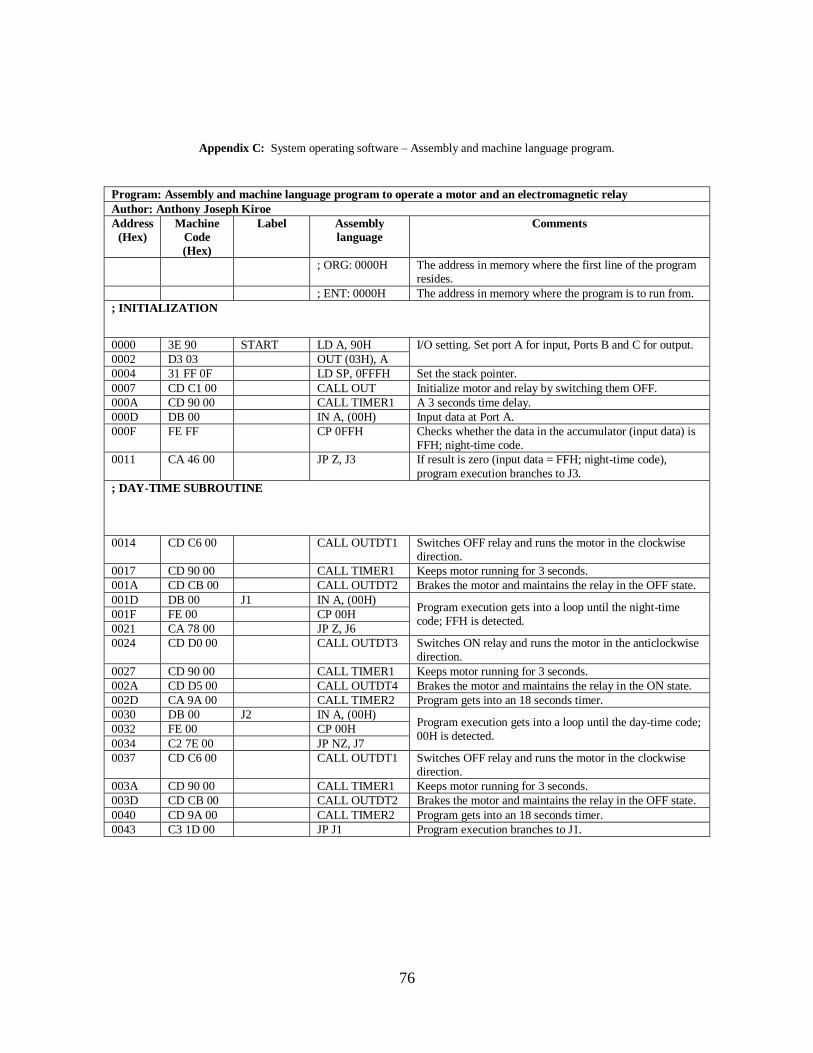
76
Appendix C: System operating software – Assembly and machine language program.
Program: Assembly and machine language program to operate a motor and an electromagnetic relay
Author: Anthony Joseph Kiroe
Address
(Hex)
Machine
Code
(Hex)
Label Assembly
language
Comments
; ORG: 0000H The address in memory where the first line of the program resides.
; ENT: 0000H The address in memory where the program is to run from.
; INITIALIZATION
0000 3E 90 START LD A, 90H I/O setting. Set port A for input, Ports B and C for output.
0002 D3 03 OUT (03H), A
0004 31 FF 0F LD SP, 0FFFH Set the stack pointer.
0007 CD C1 00 CALL OUT Initialize motor and relay by switching them OFF.
000A CD 90 00 CALL TIMER1 A 3 seconds time delay.
000D DB 00 IN A, (00H) Input data at Port A.
000F FE FF CP 0FFH Checks whether the data in the accumulator (input data) is FFH; night-time code.
0011 CA 46 00 JP Z, J3 If result is zero (input data = FFH; night-time code),
program execution branches to J3.
; DAY-TIME SUBROUTINE
0014 CD C6 00 CALL OUTDT1 Switches OFF relay and runs the motor in the clockwise direction.
0017 CD 90 00 CALL TIMER1 Keeps motor running for 3 seconds.
001A CD CB 00 CALL OUTDT2 Brakes the motor and maintains the relay in the OFF state.
001D DB 00 J1 IN A, (00H) Program execution gets into a loop until the night-time code; FFH is detected.
001F FE 00 CP 00H
0021 CA 78 00 JP Z, J6
0024 CD D0 00 CALL OUTDT3 Switches ON relay and runs the motor in the anticlockwise direction.
0027 CD 90 00 CALL TIMER1 Keeps motor running for 3 seconds.
002A CD D5 00 CALL OUTDT4 Brakes the motor and maintains the relay in the ON state.
002D CA 9A 00 CALL TIMER2 Program gets into an 18 seconds timer.
0030 DB 00 J2 IN A, (00H) Program execution gets into a loop until the day-time code; 00H is detected.
0032 FE 00 CP 00H
0034 C2 7E 00 JP NZ, J7
0037 CD C6 00 CALL OUTDT1 Switches OFF relay and runs the motor in the clockwise direction.
003A CD 90 00 CALL TIMER1 Keeps motor running for 3 seconds.
003D CD CB 00 CALL OUTDT2 Brakes the motor and maintains the relay in the OFF state.
0040 CD 9A 00 CALL TIMER2 Program gets into an 18 seconds timer.
0043 C3 1D 00 JP J1 Program execution branches to J1.
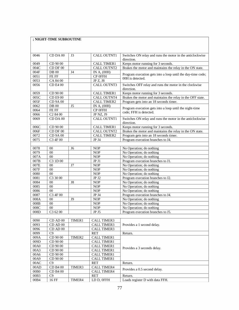
77
; NIGHT-TIME SUBROUTINE
0046 CD DA 00 J3 CALL OUTNT1 Switches ON relay and runs the motor in the anticlockwise direction.
0049 CD 90 00 CALL TIMER1 Keeps motor running for 3 seconds.
004C CD DF 00 CALL OUTNT2 Brakes the motor and maintains the relay in the ON state.
004F DB 00 J4 IN A, (00H) Program execution gets into a loop until the day-time code; 00H is detected.
0051 FE FF CP 0FFH
0053 CA 84 00 JP Z, J8
0056 CD E4 00 CALL OUTNT3 Switches OFF relay and runs the motor in the clockwise direction.
0059 CD 90 00 CALL TIMER1 Keeps motor running for 3 seconds.
005C CD E9 00 CALL OUTNT4 Brakes the motor and maintains the relay in the OFF state.
005F CD 9A 00 CALL TIMER2 Program gets into an 18 seconds timer.
0062 DB 00 J5 IN A, (00H) Program execution gets into a loop until the night-time code; FFH is detected.
0064 FE FF CP 0FFH
0066 C2 84 00 JP NZ, J9
0069 CD DA 00 CALL OUTNT1 Switches ON relay and runs the motor in the anticlockwise direction.
006C CD 90 00 CALL TIMER1 Keeps motor running for 3 seconds.
006F CD DF 00 CALL OUTNT2 Brakes the motor and maintains the relay in the ON state.
0072 CD 9A 00 CALL TIMER2 Program gets into an 18 seconds timer.
0075 C3 4F 00 JP J4 Program execution branches to J4.
0078 00 J6 NOP No Operation; do nothing
0079 00 NOP No Operation; do nothing
007A 00 NOP No Operation; do nothing
007B C3 1D 00 JP J1 Program execution branches to J1.
007E 00 J7 NOP No Operation; do nothing
007F 00 NOP No Operation; do nothing
0080 00 NOP No Operation; do nothing
0081 C3 30 00 JP J2 Program execution branches to J2.
0084 00 J8 NOP No Operation; do nothing
0085 00 NOP No Operation; do nothing
0086 00 NOP No Operation; do nothing
0087 C3 4F 00 JP J4 Program execution branches to J4.
008A 00 J9 NOP No Operation; do nothing
008B 00 NOP No Operation; do nothing
008C 00 NOP No Operation; do nothing
008D C3 62 00 JP J5 Program execution branches to J5.
0090 CD AD 00 TIMER1 CALL TIMER3
Provides a 1 second delay. 0093 CD AD 00 CALL TIMER3
0096 CD AD 00 CALL TIMER3
0099 C9 RET Return.
009A CD 90 00 TIMER2 CALL TIMER1
Provides a 3 seconds delay.
009D CD 90 00 CALL TIMER1
00A0 CD 90 00 CALL TIMER1
00A3 CD 90 00 CALL TIMER1
00A6 CD 90 00 CALL TIMER1
00A9 CD 90 00 CALL TIMER1
00AC C9 RET Return.
00AD CD B4 00 TIMER3 CALL TIMER4 Provides a 0.5 second delay.
00B0 CD B4 00 CALL TIMER4
00B3 C9 RET Return.
00B4 16 FF TIMER4 LD D, 0FFH Loads register D with data FFH.
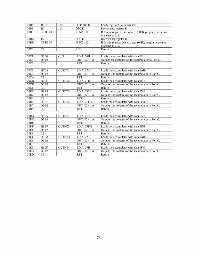
78
00B6 1E FF J10 LD E, 0FFH Loads register E with data FFH.
00B8 1D J11 DEC E Decrements register E.
00B9 C2 B8 00 JP NZ, J11 If data in register E is not zero (00H), program execution
branches to J11.
00BC 15 DEC D Decrements register D.
00BD C2 B6 00 JP NZ, J10 If data in register D is not zero (00H), program execution branches to J10.
00C0 C9 RET Return.
00C1 3E 00 OUT LD A, 00H Loads the accumulator with data 00H.
00C3 D3 02 OUT (02H), A Outputs the contents of the accumulator to Port C.
00C5 C9 RET Return.
00C6 3E 0A OUTDT1 LD A, 0AH Loads the accumulator with data 0AH.
00C8 D3 02 OUT (02H), A Outputs the contents of the accumulator to Port C.
00CA C9 RET Return.
00CB 3E 0F OUTDT2 LD A, 0FH Loads the accumulator with data 0FH.
00CD D3 02 OUT (02H), A Outputs the contents of the accumulator to Port C.
00CF C9 RET Return.
00D0 3E F5 OUTDT3 LD A, 0F5H Loads the accumulator with data F5H.
00D2 D3 02 OUT (02H), A Outputs the contents of the accumulator to Port C.
00D4 C9 RET Return.
00D5 3E FF OUTDT4 LD A, 0FFH Loads the accumulator with data FFH.
00D7 D3 02 OUT (02H), A Outputs the contents of the accumulator to Port C.
00D9 C9 RET Return.
00DA 3E F5 OUTNT1 LD A, 0F5H Loads the accumulator with data F5H.
00DC D3 02 OUT (02H), A Outputs the contents of the accumulator to Port C.
00DE C9 RET Return.
00DF 3E FF OUTNT2 LD A, 0FFH Loads the accumulator with data FFH.
00E1 D3 02 OUT (02H), A Outputs the contents of the accumulator to Port C.
00E3 C9 RET Return.
00E4 3E 0A OUTNT3 LD A, 0AH Loads the accumulator with data 0AH.
00E6 D3 02 OUT (02H), A Outputs the contents of the accumulator to Port C.
00E8 C9 RET Return.
00E9 3E 0F OUTNT4 LD A, 0FH Loads the accumulator with data 0FH.
00EB D3 02 OUT (02H), A Outputs the contents of the accumulator to Port C.
00ED C9 RET Return.