designing materials with machine learning and quantum
TRANSCRIPT

Designing materials with machine learning and quantum annealing
Koji TsudaUniversity of Tokyo / NIMS / RIKEN

Automatic Materials Design
Machine Learning
Simulation(DFT etc) Experiments
Experimental Design
Data

• Bayesian Optimization• Design of Si-Ge nanostructures (Ju+, PRX
2017)
• Wavelength selective thermal radiator (Sakurai+, ACS Cent Sci, 2019)
• D-wave quantum annealer (Kitai+, Arxiv, 2019) 3
Agenda

Bayesian Optimization(Jones et al., 1998)
• Find best data points with minimum number of observations
• Choose next point to observe to discover the best ones as early as possible

Screening by first principles calculations alone
Mat.�
Mat.�
Mat.�
Mat.�
Mat.�
Mat.�
Mat.�
Mat.
Mat.
Mat.��
First Principles Calc.
Score 1
Score2
Score 3
Score 4
Score 5
Score 6
Score 7
Score 8
Score9
Score 10
5

Bayesian Optimization (1)
Mat.�
Mat.�
Mat.�
Mat.�
Mat.�
Mat.�
Mat.�
Mat.
Mat.
Mat.��
First Principles Calc.
Score 1
Score 2
Score 3

Bayesian Optimization (2)
First Principles Calc.
Score 1
Score 2
Score 3
Pred.Score4
Pred.Score5
Pred.Score6
Pred.Score7
Pred.Score8
Pred.Score9
Pred.Score10
Var. 4
Var.5
Var.6
Var.7
Var.8
Var.9
Var.10
Mat.�
Mat.�
Mat.�
Mat.�
Mat.�
Mat.�
Mat.�
Mat.
Mat.
Mat.��
Predicted Scores
Predicted Variances

Bayesian Optimization (3)
�����
�����
�����
����
����
����
�����
�����
�����
������
Score 1
Score 2
Score 3
Score 8
First Principles Calc.
8

Bayesian Optimization (4)
�����
�����
�����
����
����
����
�����
�����
�����
������
Score 1
Score 2
Score 3
Score 8
Pred.Score4
Pred.Score5
Pred.Score6
Pred.Score7
Pred.Score9
Pred.Score10
First Principles Calc.
Var. 4
Var. 5
Var. 6
Var. 7
Var. 9
Var. 10
9

Where to observe next?
Measured Value
Explanatory Variable
CurrentMaximum
10

Gaussian Process
11
CurrentMaximum
Explanatory Variable
Measured Value

Maximum probability of improvement
12Explanatory Variable
Measured Value
CurrentMaximum
Department of Mechanical Engineering, Thermal Energy Engineering Lab 13
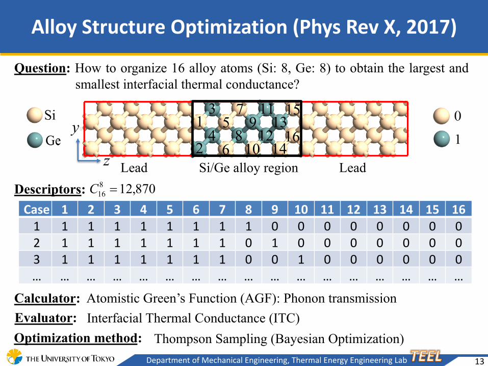
Alloy Structure Optimization (Phys Rev X, 2017)
Case 1 2 3 4 5 6 7 8 9 10 11 12 13 14 15 161 1 1 1 1 1 1 1 1 0 0 0 0 0 0 0 02 1 1 1 1 1 1 1 0 1 0 0 0 0 0 0 03 1 1 1 1 1 1 1 0 0 1 0 0 0 0 0 0… … … … … … … … … … … … … … … … …
Descriptors:
Calculator: Atomistic Green’s Function (AGF): Phonon transmission
Question: How to organize 16 alloy atoms (Si: 8, Ge: 8) to obtain the largest andsmallest interfacial thermal conductance?
870,12816 =C
Optimization method: Thompson Sampling (Bayesian Optimization) Evaluator: Interfacial Thermal Conductance (ITC)
Si/Ge alloy regionLead Lead
1
2
3
45
6
7
89
10
11
1213
14
15
16y
z

Department of Mechanical Engineering, Thermal Energy Engineering Lab 14
Alloy Structure Optimization
ITC Si-Si Si-Ge
Max
Min
Optimal structures were obtained by calculating only 3.4% of all candidates.

Department of Mechanical Engineering, Thermal Energy Engineering Lab 15
Wavelength selective thermal radiator
Solar absorber Sky radiator Heater for drying
Sakurai Lab (Nigata Univ)

Designing layered material
• 18 layers: Ge, Si or Si02
• Total thickness: 21 grid points between 3.6 μmand 4.0 μm
• Number of candidate structures: 318 x 21 = 8,135,830,269
3
2
1
Substrate
N
N-1
N-2
��
��
z
x
dt
ttotal

What to optimize
• Figure of Merit– Appreciates peaks near
target, penalizes peaks outside
• Calculation of emissivity spectra– Electromagnetic
simulation via transfer matrix method

Optimal solution found with 168 million calculations on average
(2.06% of all possibilities)
24 cores, 24 days
Target: 6.0 μm

Target: 5.0 μm Target: 7.0 μm

CalculatedExperimental Validation

Experimental Validation
Layer ThicknessTEM image

Comparison with Existing Materials
• Q-factor: Peak sharpness
• Our material: Q=273 (Simulation), Q= 188
(Realized)
• Highest known Q-factor: 200 (2D grating
coupled surface phonon polaritons, 2008)
– Large unwanted peaks: Poor FOM = 0.02
– High cost for nanofabrication

Quantum annealing
• Solves quadratic unconstrained binary optimization (QUBO)
• D-wave 2000Q – Implementation of quantum annealing with
superconducting semiconductor
– Annealing time 170μs, up to 64 bits
– Machine in Canada, accessed via API from Japan

Principle of quantum annealing
• QUBO + transverse field term
• Qubit has distribution of up and down
• When measured, up or down appears
• First, strong transverse field is applied– [up,down] = [0.5,0.5] is the ground state
• Then transverse field is weakened slowly– Ground state slides to global optimum of QUBO
• Conceptually similar to regularization path following (?)

Using QA for black-box optimization
• GP’s acquisition function is not QUBO (BAD!)• Use factorization machine instead
• A learned model becomes QUBO• 50 annealing at a time, select the best unseen
solution


Comparison to existing materials

Conclusion• Designing complex materials is beyond ability
of human intuition• New “class” of materials enabled by ML & QA
• Tsuda Lab, UTokyo• Koki Kitai• Ryo Tamura
• Dept of Mech Eng, UTokyo• Junichiro Shiomi• Takuma Shiga• Shenghong Ju• Lei Fang• Jiang Guo• Makoto Kashiwagi
• Niigata Univ• Atsushi Sakurai• Kyohei Yada• Hideyuki Okada• Tetsushi Shimomura
• NIMS• Zhufeng Hou• Tadaaki Nagao
• Waseda Univ• Shu Tanaka