designing multisocket systems with silicon photonics
TRANSCRIPT

Designing Multisocket Systems with Silicon Photonics
by Scott Beamer
Research Project
Submitted to the Department of Electrical Engineering and Computer Sciences,University of California at Berkeley, in partial satisfaction of the requirements forthe degree of Master of Science, Plan II.
Approval for the Report and Comprehensive Examination:
Committee:
Professor Krste AsanovicResearch Advisor
(Date)
* * * * * * *
Professor David A. PattersonSecond Reader
(Date)

Abstract
To fuel an increasing need for parallel performance, system designers have resulted to using multi-ple sockets to provide more hardware parallelism. These multisocket systems have limited off-chipbandwidth due to their electrical interconnect which is both power and pin limited. Current sys-tems often use of a Non-Uniform Memory Architecture (NUMA) to get the most system memorybandwidth from limited off-chip bandwidth. A NUMA system complicates the work of a perfor-mance programmer or operating system, because they must maintain data locality to maintainperformance.
Silicon photonics is an emerging technology that promises great off-chip bandwidth densityand energy efficiency when compared to electrical signaling. With this abundance of bandwidth,it will be possible to build a relatively flat, high bandwidth memory interconnect. Because thisinterconnect has uniform bandwidth, NUMA optimizations will be unnecessary, which increasesperformance programmer productivity.
If the penalties to making a multi-socket system are negated by the use of silicon photonics,there is less incentive to integrate, and economic incentives to disintegrate. In this thesis, wepresent this scalable and coherent multi-socket design along with discussing the tradeoffs facing anarchitect when incorporating silicon photonics technology.

Chapter 1
Introduction
Given the difficulties of scaling uniprocessor performance further, most commercial microprocessormanufacturers have instead used increased transistor densities to integrate multiple processor coreson one die [1]. These manycore systems will require increasing memory bandwidth at reasonableenergy consumption if they are to deliver improvements in application performance. Otherwisethese systems may be grossly underutilized [27].
When the desired number of cores cannot fit on a die that is economical to manufacture, they arespread across multiple sockets. To feed many cores spread across multiple sockets will require evenmore memory bandwidth. Each socket will have its own attached DRAM, but in a shared memorymachine it must be made accessible to the other sockets within the system. This interconnect musthave an on-chip portion that connects all of the cores within a socket in addition to an off-chipportion that connects all the sockets within the system.
Current multisocket systems often have their off-chip bandwidth constrained by power and pinlimitations [14, 18, 23]. As more cores are integrated into a die within a socket, they will needeven more bandwidth, and this bottleneck will become more troublesome as it is unlikely off-chipelectrical bandwidth will be able to keep up. The energy required to send a bit between socketsis not scaling down very quickly because the sockets are not getting much closer physically, andthe materials used for traces is not getting significantly less resistive or capacitive. Even if off-chipelectrical signaling becomes sufficiently more energy efficient, pin bandwidth could become the nextlimiting factor. Off-chip signaling rates and die sizes are not growing fast enough to provide enoughpin bandwidth to meet the growing demand.
A socket’s limited off-chip bandwidth must be divided up between links to its own locally at-tached DRAM and inter-socket links to reach remote DRAM attached to other sockets (Figure 1.1).If all of the bandwidth is allocated to the locally attached DRAM, the system will have the max-imum memory bandwidth possible, but it will be disjoint. In contrast, if all of the bandwidth isallocated to the inter-socket links, the system will have no memory bandwidth but great inter-corebandwidth. If the two are balanced uniformly such that each socket receives an equal amount ofbandwidth from every part of memory (remote or local) the system will have a Uniform MemoryArchitecture (UMA), and if they are balanced non-uniformly, the system will have a Non-UniformMemory Architecture (NUMA).
Systems trying to get the most system memory bandwidth while coping with off-chip bandwidthscarcity will be pushed towards a NUMA design. This is true independent of the off-chip networktopology, because each inter-socket link occupies bandwidth at two sockets, while a link to DRAM
1

only occupies bandwidth at one socket. Any bandwidth taken away from the inter-socket links,can be turned into twice the bandwidth for the links to DRAM. This encourages system designersto skew the bandwidth allocations in favor of locally attached DRAM instead of reaching othersockets, to maximize system memory bandwidth.
ComputeChip
DRAM
ComputeChip
DRAM
ComputeChip
DRAM
DRAM
ComputeChip
DRAM
DRAM
!"#$%&'()*"+,#+-.
*/
0%"1!"#$%&'()*"+,#+-.
2/
Figure 1.1: Motivation for NUMA
A NUMA design imposes additional complexity on the performance programmer, as it is crucialthat data is co-located with the computation using it. This careful mapping is yet another opti-mization performance programmers must consider [27], but if the memory system was flat (uniform)it would be unnecessary, increasing their productivity. Some multiprogrammed workloads, such asvirtual machines running within a datacenter, will also benefit from the scheduling flexibility thatbandwidth uniformity provides. When scheduling jobs, a job could be run on the first availablecore independent of where the data it needs resides. Furthermore, some workloads exhibit poorspatial locality so it is difficult to spread the data across sockets effectively. If a new technologyprovided an abundance of bandwidth, it would be worthwhile to allocate it uniformly to increaseprogrammer productivity and make the system more flexible.
In this work, we leverage silicon photonics to design high and uniform bandwidth multi-socketmemory interconnects. We present a general network design that can be used to make systemsof varying sizes, and to provide shared memory which makes the system more usable, we discusshow to reasonably implement coherency on top of the network. Because of the nature of thedesign, it has much less incentive to integrate, which opens the door to chip disintegration forcost savings. Overall, multi-socket interconnects are an interesting place to explore applications ofcurrent research in silicon photonics because of its emphasis on off-chip communication.
2

Chapter 2
Photonic Technology Introduction
Over the last few decades, the scale at which optical technology has been adopted for commu-nication has been steadily decreasing. Optical communication was first used for long distancetelecommunications, because its high endpoint costs were amortized over very long links. As pro-cessing technologies have improved, the cost (delay, space, energy, dollars . . . ) of the endpointshave decreased, which in turn has decreased the distance at which optical communication is ad-vantageous. Continued technology advances along with increased integration have enabled siliconphotonics, which decreases the feasible distance down to the inter-chip and even intra-chip level.
2.1 Technology Overview
In recent years, silicon photonics has been shown to be an increasingly desirable technology for sys-tem interconnects because of its potential for higher bandwidth density, greater energy efficiency,and lower latency. The technology is still immature with many competing implementation propos-als, so projected performance on these important metrics varies significantly. To ground the resultsof our study, we select a particular monolithically integrated silicon photonics technology [4], butthe overall approach should be applicable to the other current proposals because much of it is basedon general technology insights.
Figure 2.1 shows a basic link is comprised of: a light source, a modulator, a waveguide, and aphotodetector. The modulator encodes the signal by absorbing or not absorbing light as it passesby it through the silicon waveguide. At the other end of the waveguide, the photodetector sensesthe changes in light and decodes the signal. The electro-optical and opto-electrical conversions atthe endpoints introduce a latency and energy cost that needs to be amortized beyond a minimumdistance to be advantageous to electrical.
Off-chipLaser
VerticalCoupler
Die 1 Die 2Photodetector
Ring Filter
RingModulator Fiber
Waveguide
Figure 2.1: An inter-socket photonic link
3

The selected technology provides Dense Wave Division Multiplexing (DWDM) which contributesto its high bandwidth density (bits/second/ µm). DWDM allows light from different wavelengthsto share the same waveguide with minimal interference, which allows multiple logical links to sharethe same physical media without time multiplexing. This is enabled by putting rings which resonatewith a narrow frequency of light onto the waveguide, such that when the light resonates with a ring,it is pulled off the waveguide into the ring. We can use these rings along with charge injection tomake a ring modulator [11, 20, 21]. Applying a charge to a ring shifts the ring’s resonant frequencyso a particular wavelength can be absorbed or not absorbed to modulate the light.
A filter can also be made by using these resonant rings [21, 26], and the selected technologyuses two cascaded rings to get additional frequency selectivity (Double Ring Filter). Since thephotodetectors are sensitive to a wide range of light frequencies, a double ring filter is placedbetween the photodetector and the waveguide so only the correct wavelength gets through thefilter and strikes the photodetector. These resonant rings are sensitive to a variety of environmentalfactors and manufacturing variations, but these can be combated by thermally tuning the rings within-plane heaters.
The selected technology is monolithically integrated, and it utilizes a current CMOS manufac-turing process which makes it much more realizable since it leverages a great deal of manufacturinghardware investment and knowledge. Other photonic proposals may be better suited for transmit-ting light, but they use materials or steps not currently part of a standard CMOS process makingthem more cost prohibitive to implement [3, 11, 15].
The light used by the system is generated by an off-chip laser because conventional CMOSprocesses are poorly suited for laser fabrication. This light is brought on chip through a fiberand then a coupler into the waveguide. On-chip light travels through poly-Si, which can be madeinto a usable waveguide (Figure 2.2) by placing it on top of shallow trench isolation (STI) andetching an air gap underneath it [10]. The air gap helps to improve the cladding on the bottom ofthe waveguide, because the STI is too thin on its own. The air gap does take up silicon area, sowhen possible multiple waveguides should share one to amortize the overhead. A great advantageof photonics is that once the signal has been encoded optically, that light can be guided throughthrough couplers and a fiber to another chip’s waveguide without retransmission (Figure 2.1),enabling links that operate seamlessly across long distances.
STI
BackendDielectric
SiliconSubstrate
Poly-SiWaveguide
Air Gap
Etch
Hol
e
MOSFET
Figure 2.2: Cross section of an on-chip waveguide
4

2.2 Performance
Looking forward to when this silicon photonic proposal might be fully realizable, we compare itagainst a projected optimally repeated electric wire in a 22nm process and Tables 2.1, 2.2, and 2.3give a summary of the comparison. Based on preliminary results and device projections, the siliconphotonic proposal assumes a signaling rate of 10Gbps (faster could be possible) and squeezes in 64wavelengths per direction [21], meaning a single link (fiber or waveguide) has 80GB/s of bidirectionalbandwidth.
Table 2.1: Approximate energy costs per bit
Quantity Electric (fJ) Photonic (fJ) RatioOn-Chip Model 50 fJ
mm 1501
Off-Chip Model 5000 150Local On-Chip Wire (1µm) 0.05 150 0.00033Intermediate On-Chip Wire (1mm) 50 150 0.33Global On-Chip Wire (10mm) 500 150 3.33Off-Chip Trace (40mm) 5000 150 33.33Chip-to-Chip Link 5500 150 33.67
(40mm off-chip, 10mm on-chip)
Table 2.2: Approximate latency costs per bit
Quantity Electric (ps) Photonic (ps) RatioOn-Chip Model 100 ps
mm 200 + 10 psmm
Off-Chip Model 50 + 5 psmm 200 + 5 ps
mmLocal On-Chip Wire (1µm) 0.1 200.01 0.0005Intermediate On-Chip Wire (1mm) 100 210 0.48Global On-Chip Wire (10mm) 1000 300 3.33Off-Chip Trace (40mm) 250 400 0.63Chip-to-Chip Link 1250 700 1.79
(40mm off-chip, 10mm on-chip)
Table 2.3: Approximate bandwidth densities per bit. Photonic values sum the bandwidth of bothdirections
Electric (Gb/s/ µm) Photonic (Gb/s/ µm) RatioOn-Chip 5 320 64.0Off-Chip 0.2 26 130.0
1100 fJb (modulator) + 50 fJ
b (receiver) + 80uW (power to thermally tune rings) + optical power
5

2.2.1 Power
Energy efficiency ( bits/secW = bits
J ), especially off-chip, has been listed as one of the strongest advan-tages of the selected photonic technology. It is important to fully explore the three ways it expendspower:
• Encoding/Decoding power is consumed at the endpoints and it includes electrical circuits toserialize/deserialize the signal from the native system clock to the transmission rate as wellas the power consumed by charge injection to modulate the signal. This power is insensitiveto distance, is mostly dynamic, and the values quoted in Table 2.1 are for 100% utilization.
• Light Generation power is burned by the laser to produce the light used for communication.This power is constant, independent of utilization. It is difficult to dynamically adjust laserpower. To generate laser light more efficiently, the same laser is used for multiple links, sounless all of the links are inactive, it is hard to scale back. It is important to note that thelight generation power is the amount of electrical power required to produce the laser power(light intensity) the system needs. Light generation power is often overlooked, and most ofthe prior work has not added it to the power total with the justification that it is off chipand thus does not contribute to power density hotspots on the processor [25]. Keeping withconvention, for most of this work laser power will be presented separately, because laser lightgeneration is an orthogonal area of research, so converting it to electrical power might bemisleading. However, when calculating the total power for a system, a conservative estimateof future laser efficiency of 25% is used. This power is strongly dependent on how much lossthe path has, and Section 2.3 will present more details about this.
• Thermal Tuning power is burned up by heaters to control the ring’s resonant frequency forprocess variation. The observed sensitivity is 1µW/ring/K and the needed control range is20K, so each ring will burn 20µW .
In summary, using a silicon photonic link purely on-chip will not be significantly advantageouswith regards to energy, unless it travels a substantial distance (> 3mm), however off-chip it couldbe more than an order of magnitude more efficient.
2.2.2 Latency
Most of the latency for a silicon photonic link is at the endpoints, since light propagates rapidly.The endpoint latency is a consequence of serializing and deserializing the data from the native clockrate to the transmission rate of 10 Gbps. Table 2.2 shows that photonics only has lower latencythan electrical beyond 2.2mm on-chip. As mentioned earlier, the photonic links can go inter-chipwithout retransmission, so in those cases the latency gap between electric and photonic is furtherreduced.
2.2.3 Area
On-chip waveguides are larger than wires and they have a wider pitch. The air gaps makes thewaveguides effectively wider because no circuits can be placed over them. Even though waveguidestake up more area than wires, there is so much more bandwidth per waveguide from DWDM andbidirectional communication that it still obtains a large bandwidth density advantage (Table 2.3).
6

Off-chip this advantage becomes more significant because they have comparable pitches, with thesame data rates, but a single fiber contains 64 links in each direction while an electrical pin onlyimplements a single link in one direction.
2.3 Laser Power
Every optical component introduces some amount of loss to the signal, increasing the laser powerneeded to ensure sufficient light reaches every photodetector. As mentioned, in 2.2.1, light genera-tion power is significant, and it is directly proportional to laser power. We define the optical criticalpath as the path with the greatest loss between the light source and the last photodetector. Alongthe optical critical path, the laser power required to overcome losses tends to grow exponentiallyrather than linearly, so a reasonable design can quickly become unreasonable when scaled up. Thenetwork layout and size can contribute greatly to loss, so careful physical layout design is essentialto save power.
Using Figure 2.3, we can trace out an example optical critical path and show where the lossescome from. Table 2.4 is included to give sense of the relative magnitudes, since the absolute valuescould change as the technology matures. The optical critical path starts at the laser, and endsat the last photodetector (the one attached to the filter for the green wavelength). Traveling anydistance, the light experiences some loss, which is negligible for off-chip fibers and significant foron-chip waveguides. To go from from off-chip to on-chip or vice versa, the light travels through acoupler, which incurs loss substantial enough that links which span more than two chips may beuntenable. Once the light has been brought on-chip, it typically is fanned out through splittersto make all of the needed links. When the waveguide crosses another waveguide, it also incursloss because all waveguides are routed in the same plane with this technology. Crossing losses canbe significant, because often multiple waveguides are routed parallel to each other, so a crossingactually results in many crossings.
There are a variety of losses caused by the resonant rings. When light passes by a filter tuned foranother wavelength, it experiences through loss (Filter to through node). When it passes throughthe intended filter and reaches the photodetector, it experiences drop loss (Filter to drop node).Modulator insertion loss is incurred when a wavelength of light passes by a modulator tuned forthat frequency that is currently inactive.
Another important consideration is the non-linearity limit imposed by the Poly-Si waveguide.As the combined power of the light inside a waveguide grows, there is a non-linear increase inthe amount of light that escapes. To combat that loss, more laser power is used which resultsin even more loss, so its best to keep the total power for a waveguide within reasonable limits.Normally how many wavelengths can be put into a waveguide is set by the frequency selectivityof the photonic components used, but the number of wavelengths used per waveguide may also beset by the path loss which determines the power required per wavelength and thus the number ofwavelengths that can fit under the non-linearity limit. The designs presented later in this studywere made to have low loss, and they should be able to carry 64 wavelengths per direction withoutissue.
7

Off-chipLaser
Chip
CouplerLoss
SplitterLoss
ModulatorInsertionLoss
CrossingLoss
ThroughLoss
DropLoss
WaveguideLoss
Figure 2.3: Photonic link with with losses labelled for the green wavelength
Table 2.4: Optical Power Costs [4]
Component Loss (dB)Coupler 1.0Splitter 0.2Non-Linearity 1.0Filter (to through node) 0.01Modulator Insertion 0.5Waveguide Crossing 0.05Waveguide (per cm) 1.0Optical Fiber (per cm) 0.000005Filter (to drop node) 1.5Photodetector 0.1
8

2.4 Design Implications
As shown by Tables 2.1 & 2.3, the selected photonics technology can provide a tremendous amountof off-chip bandwidth, because of its energy efficiency and bandwidth density advantages. Replacingthe electrical inter-socket links with photonic ones will enable much more bandwidth to each socket.Used in conjunction with an electrical on-chip network, it could still result in dramatically highersystem bandwidth.
Even though entirely on-chip photonic links do not hold much of an advantage over electricalon-chip links, if photonics is used for the off-chip network, it makes sense to continue seamlesslyon-chip because the conversions costs will have already been paid. By using these seamless links,off-chip networks and on-chip networks are flattened into one domain. To get the most from thisflat network will require co-design of the on-chip and off-chip networks.
In this thesis, the connection between a memory controller and a DRAM module is assumedto be electrical. Future work could investigate a photonic link between a memory controller andDRAM, and doing so should not change the results of this study.
9

Chapter 3
Design of a Photonic Multisocket
System
Section 2 shows that silicon photonics has great potential, and in this section we present a networkdesigned to take full advantage of it. When designing a system known to be multi-socket, it isimportant to consider the off-chip network in addition to the on-chip network, and co-designing theon-chip and off-chip networks makes best use of seamless photonic links.
3.1 System Assumptions
To provide structure for the rest of this study, we make some assumptions about the target system.There are a variety of architectures that could take advantage of the transistor gains from Moore’slaw, but to achieve high computational throughput on a workload without high arithmetic intensity,they will all require high memory bandwidth. For this work, we envision a system comprised ofmany simple in-order cores, but some of the higher level results should still be applicable to otherarchitectures.
To ground our design with real numbers (Table 3.1), we assume in a 22 nm process with 400mm2
of silicon, it will be possible to fit 256 cores running at 2.5GHz [4]. Each of these cores will include4-way SIMD with Fused Multiply Accumulate (FMAC), giving the the system a total of 5 TFLOPSof peak performance. The amount of memory bandwidth needed to adequately supply this systemwill depend on the arithmetic intensity of the target workload, but the frequently desired ratio of onebyte of memory bandwidth per one flop will support many desired workloads, which will equate to5 TBps of memory bandwidth for the system [27]. This bandwidth will be supplied by 16 memorycontrollers, and each of these memory controllers may be attached to multiple physical DRAMchannels, but from the point of view of the rest of the system, each memory controller is a singleendpoint of arbitration and contention. We also assume that this system will be implemented overfour sockets, so each socket will have one quarter of the cores and memory controllers. We assumea shared-memory system, where photonics is used to connect processor to memory controllers, notcores to cores.
10

Baseline Socket Max ConfigurationSockets 1 4Cores 64 256Clock Rate 2.5 GHz 2.5 GHzTotal Silicon Area 100 mm2 400 mm2
Memory Bandwidth 1.25 TBps 5 TBpsMemory Controllers 4 16
Table 3.1: Target system assumptions
3.2 Topology Insights
A network designer must balance the needs of the target workload with what the technology allows.The assumed workload for this system will need high bandwidth to feed many functional units,but this bandwidth must be provided uniformly (equally by all memory controllers) to simplifyprogramming and to increase portability. Memory latency must be keep moderately low since thecores are mostly scalar, so they are incapable of cheaply tolerating too much memory latency. ByLittle’s Law, the amount of data in flight is proportional to the product of latency and bandwidth.If the memory latency is increased, additional area will need to be dedicated to holding and trackingthe increased amount of data in flight, which will make the simple cores more expensive.
A low-diameter, high-radix network will achieve these goals, and it will map well to the selectedsilicon photonics technology proposal. Low-diameter networks are known for low latency due totheir low hop count, as well as having more uniform latency because there is less variance in pathlength [8]. This low hop count also results in more uniform bandwidth because there are less hopsfor links to get congested by other traffic on the network. To reach the same number of endpoints,a lower-diameter network must compensate with a higher radix. With a constant bandwidth perendpoint, increases in radix result in decreased bandwidth per link, which can be problematic as itwill increase the serialization latency.
A common challenge with implementing low-diameter, high-radix networks in electrical tech-nologies is that the links tend to become longer, and as a consequence, consume a significant amountof power. The selected photonic technology, however, is mostly distance insensitive with respect tolatency and power. Another challenge with implementing these global links is that when mappedto a physical substrate, the bisection bandwidth required is high. This can be troublesome to routeoff-chip, but fortunately the selected photonic technology provides great off-chip bandwidth den-sity. In contrast, if this network was implemented electrically, the bisection bandwidth would beconstrained by the electrical pins, limiting the total network bandwidth. This would encourage thenetwork designer to use a higher-diameter, lower-radix network to reduce the demand for bisectionbandwidth which will also reduce the demand for off-chip bandwidth, at the price of longer andless uniform latencies and less uniform bandwidths.
Our design takes the low-diameter, high-radix network to the extreme, by using a simple fully-connected network (Figure 3.1a) as a starting point. Each network endpoint (core or memorycontroller), will have a high-radix switch with a photonic link for every possible endpoint. A singlephotonic hop minimizes latency while maximizing bandwidth uniformity. A one-hop topology willbecome a limiting factor as the design is scaled up to higher numbers of endpoints, since it will alsoincrease the radix. Increasing the radix will hurt performance because the serialization latency will
11

grow as the links get narrower, and the power and area for the electrical switch will grow as itsradix does. For the intended design scale of a single-board, compelling systems might be possibleutilizing the selected photonic technology without taking up an unreasonable amount of area orpower.
C
L1
Memory Controller
S
L2
S
C
L1
S
L2
C
L1
Memory Controller
S
L2
S
C
L1
S
L2
C
L1
Memory Controller
S
L2
S
C
L1
L2
C
L1
Memory Controller
S
L2
S
C
L1
L2
C
L1
Memory Controller
S
L2
S
C
L1
Memory Controller
S
S
C
L1
L2
C
L1
!" #" $"
Figure 3.1: Topological benefits of concentration. a: Fully-connected network b: Fully-connectednetwork with core concentration c: Fully-connected network with core concentration done by ashared cache
3.2.1 Concentration
Taking the simple initial design of a fully connected topology between individual cores and memorycontrollers and scaling it to meet the target system parameters will result in poor performance.The effective radix is high because there are so many memory controllers and cores, making eachcore–memory controller link so narrow (for the target system: 1
16th of a core’s bandwidth) that the
serialization latency is significant. It is also statistically harder for a simple core to have enoughmemory request parallelism to keep all of those links busy simultaneously, leaving many of themunderutilized. Low utilization is worrisome because static power constitutes a large fraction of aphotonic link’s power, but this can be avoided by using concentration to share links to increaseutilization [8].
By grouping cores into clusters (Figure 3.1b), concentration widens the links to the memorycontrollers, which drastically cuts down on serialization latency. Since each cluster contains multiplecores, within in a cluster it is statistically easier to generate enough memory request parallelismto obtain higher utilization. Concentration combines the switches and links at the core side ofthe network to reduce the effective radix of the network. This has the desired effect of improvingserialization latency, but it could also be used to build larger networks with the same serializationlatency.
Since the cores within a cluster will be physically near each other as they share the samephotonic cluster–memory links, they could also share their last level cache (Figure 3.1c). There arearchitectural benefits of sharing a cache, and current caches have been built with 8-way sharing[17]. These short links between cores and caches, and caches and the local switch should electrical,since it is too short of a distance for photonics to be advantageous. For the rest of our designs we
12

assume 8–core clusters, which obtains the benefits of concentration without overly burdening thecluster interconnect, but clusters of 2–16 cores should also be feasible.
3.2.2 Off-Chip Connections
With multi-socket systems it is desirable if the same chip can be used by simply varying the numberconnected together (even if only powers of two), because it will increase the volume of that part,lowering its cost. This scalable reusability is difficult to obtain while providing the goal of uniformmemory bandwidth. As shown in Figure 3.2a, if the connections between clusters and memorycontrollers are made on-chip, that bandwidth is fixed because we want to reuse the same chipin all systems. Using that chip to build systems with a variable number of sockets populatedwill require some bandwidth (on-chip or off-chip) be turned off to keep the bandwidth allocationbetween the memory controllers on-chip and the memory controllers in other sockets uniform. Ifevery connection is made off-chip (Figure 3.2b), the bandwidth allocations can be changed off-chipwithout modifying the chip.
Core
L1
Shared L2
Memory Controller
Core
L1
Core
L1
Core
L1
Memory Controller
Core
L1
Shared L2
Core
L1
Core
L1
Core
L1
Chip 1
Core
L1
Shared L2
Memory Controller
Core
L1
Core
L1
Core
L1
Memory Controller
Core
L1
Shared L2
Core
L1
Core
L1
Core
L1
!"#$%&'()(!*#$%&' !*#$%&'(!"+,
Chip 1Chip 2 Chip 2
-. /.
Figure 3.2: Topological benefits of all connections off-chip
To implement this, each cluster will have enough links to support the maximum number ofmemory controllers in the largest possible system, and the memory controllers will have enoughlinks to support the maximum number of clusters in the largest possible system. In a fully populatedsystem, all of these links will be connected one to one. If the system has only half of its socketspopulated, there will be two links between each cluster and each memory controller. These linkscould be ganged together to make a single logical link of twice the bandwidth, or they could be keptseparate to allow for greater memory request parallelism. In the case of a single socket system, theoff-chip fibers are looped back.
It might seem that routing all traffic off-chip is wasteful when some of it could be done purelyon-chip, but with photonics this penalty is greatly reduced. Most of the latency and on-chip energycost of a photonic link is at the endpoints, so whether the link is purely on-chip or not only affectsoptical power. Depending on what the optical critical path loss is, this change in optical power maybe truly negligible. This is in contrast to electrical off-chip links which consume sufficiently moreenergy and area such that an efficient design will never send data off-chip unless forced. Takingadvantage of the off-chip bandwidth density, energy efficiency, and distance insensitivity of photonic
13

links, for the flexibility it provides and for the uniformity it maintains, the benefits of making allconnections off-chip outweigh the small light generation power increase.
3.3 Packaging
To package the topology into a physical design will require more innovation. Because all of thecluster–memory controller connections are off-chip, each chip will have two types of fibers: thoseoriginating at clusters and those originating at memory controllers. Somehow off-chip, all of thesefibers must be appropriately attached. To keep the fibers more organized, they can be groupedinto ribbons, which simplifies assembly. As the number of sockets in the system grows, the numberof ribbons that must be attached could be become unreasonable, because the topology is fullyconnected, so each socket must a have a ribbon to every socket (including itself). Figure 3.3ashows this for the four socket case.
ComputeChip
LaserComputeChip
Laser
ComputeChip
LaserComputeChip
Laser
RibbonComputeChip
LaserComputeChip
Laser
ComputeChip
LaserComputeChip
Laser
!"#$%&#'(#)*'+",-*'.%&/0-* !"#$'(#)*'+",-*'.%&/0-*
)1 ,1
Figure 3.3: Comparison of with/without star fiber coupler
A star fiber coupler provides the needed all-to-all connectivity while greatly simplifying thefiber routing (Figure 3.3b). The star fiber coupler acts as a hub chip, so independent of systemsize, each socket only needs to attach two ribbons (one from its clusters and one from its memorycontrollers) to the coupler, and it will create the all-to-all connections. As shown in Figure 3.4, allof the cluster ribbons attach to one side of the coupler, and all of the memory controller ribbonsattach to the other side. The ribbons from both sides come in orthogonal to each other so eachribbon crosses every other ribbon. In the example shown, four ribbons of four fibers come in eachside, so effectively it is as if there is a fiber between every socket including itself (one fiber getslooped back).
The star fiber coupler can be generalized to support cases when there are more fibers thansockets or when multiple fibers are destined for each socket. It is a completely passive device,whose only purpose is to precisely hold ribbons such that their fibers can be efficiently coupled.The star fiber coupler should be comparably inexpensive, and along with some of the ribbons, arethe only things to change between different system sizes.
To lay the system out on a board, the compute dies that contain the clusters and memorycontrollers are placed around the star fiber coupler as shown in Figure 3.5a. Each of the computedies is surrounded by its own locally attached DRAM to reduce the distance for the electrical linksbetween them. The memory controllers are evenly spaced around the edge of the die to provide
14

!"#$%&'()*
+,-(./)&'()*
0123&'()*Ribbons
from Clusters
Ribbonsfrom MCs
S1
S2
S3
S4
S1 S2 S3 S4
Figure 3.4: Schematic of star fiber coupler
!"#$"%&'()*&+(*,
-./&+(*,
ComputeChip
DRAMDRAM
Laser
DRAMDRAM
ComputeChip
DRAMDRAM
Laser
DRAMDRAM
ComputeChip
DRAMDRAM
Laser
DRAMDRAM
ComputeChip
DRAMDRAM
Laser
DRAMDRAM
StarFiber
Coupler
MCRibbon
ClusterRibbon
DRAM DRAMCompute Chip
StarCoupler Optical
Ribbons
Heat Sink Laser
OpticalRibbon
"0 10
Figure 3.5: System layout
15

the easiest exposure for wiring to DRAM. By using photonics for inter-socket links, only a smallamount of area needs to be dedicated to the fibers, leaving the rest of the pin area for connectingto DRAM or attaching to power and ground. The ribbons are attached only at the endpoints byvertical couplers and the ribbons will float freely beneath the board (Figure 3.5b), so they can avoidthe heat sinks of the compute dies. A more dense board layout might reduce ribbon lengths, but itcould significantly complicate the much more costly electrical signaling to DRAM or increase thepower density. Extra distance in the ribbon is tolerable since the additional optical power loss andthe increase in delay are both negligible.
3.4 Die Layout
The layout of the photonic components on-chip is crucial because it can greatly affect the opticalpower. Without careful design, the loss along the optical critical path quickly becomes so greatthat the laser power becomes unreasonable. Essentially the designer’s job is to take all of the logicallinks, map those to wavelengths, and then map those to appropriate waveguides. The followingsections highlight the optimizations used to make an efficient layout, such as the 64 core die layoutin Figure 3.6.
Cluster Cluster
Cluster Cluster
Cluster
Cluster
Cluster
Cluster
MC
8
PowerFiber
MCRibbonClusterRibbon
8
8
8
8 Waveguidesw/ 64λ each
16
Shared L2
Shared L2
Modulators
RingFilters
Photo-detectors
16
x16
16x
8-CoreCluster
MC
MC MC
Figure 3.6: Die layout for 64 core die designed to support a 256 core system
16
3.4.1 Nested-U Waveguide Layout
Laying out the waveguides in a nested-U configuration as shown in Figure 3.6 can help combattwo sometimes avoidable sources of optical loss: waveguide length and crossing loss. By bringingthe power fiber in on one side and the inter-socket ribbons on the other, the waveguide distance isminimized while still reaching all the needed endpoints. The nested-U layout guarantees the thewaveguide distance is less than or equal to the length of the chip plus the width of the chip. Asingle crossing doesn’t contribute too much loss, but quite often waveguides are routed in parallel soa crossing will intersect multiple waveguides and then the losses multiply. Nesting the waveguidesremoves all crossings, since they always go around each other.
3.4.2 Cluster Striping Across Waveguides
With the nested-U waveguide layout, a waveguide from the power fiber to the inter-socket ribbonactually passes by more than one cluster. To load a waveguide with wavelengths from only onecluster exclusively is wasteful, because later on those wavelengths will need to be mixed for theinter-socket fibers. Striping a cluster’s wavelengths across all the waveguides that pass by reducesthe need to mix wavelengths later on.
In the example in Figure 3.6, eight waveguides pass four clusters. If each cluster put all of itswavelengths on two waveguides, somehow the wavelengths will need to be shuffled around suchthat they map appropriately to the four fibers that go between each socket. A device like theone presented in Section 4.2.1 could accomplish the needed mixing, but with striping it is oftenunnecessary.
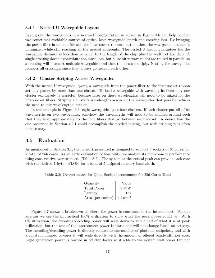
3.5 Evaluation
As mentioned in Section 3.1, the network presented is designed to support 4 sockets of 64 cores, fora total of 256 cores. As an early evaluation of feasibility, we analyze its interconnect performanceusing conservative overestimates (Table 3.2). The system at theoretical peak can provide each corewith the desired 1 byte : FLOP, for a total of 5 TBps of memory bandwidth.
Table 3.2: Overestimates for Quad Socket Interconnect for 256 Cores Total
Quantity ValueTotal Power 9.77WLatency 1nsArea (per socket) 4.2 mm2
Figure 3.7 shows a breakdown of where the power is consumed in the interconnect. For ouranalysis we use the impractical 100% utilization to show what the peak power could be. With0% utilization, the encoding/decoding power will scale down to about half of what it is at peakutilization, but the rest of the interconnect power is static and will not change based on activity.The encoding/decoding power is directly related to the number of photonic endpoints, and witha constant number of cores it will scale directly with the amount of offered bandwidth per core.Light generation power is burned in off chip lasers so it adds to the system wall power but not
17

Light Generation34%
Encoding/Decoding63%
Thermal Tuning3%
Figure 3.7: Breakdown of network power consumption for 256 core system with 64 cores per die
to the compute die’s power density. For comparison, we converted laser power to light generationpower assuming a conservative laser efficiency of 25%. Thermal tuning power is set by the numberof rings which is also directly proportional to the number of photonic endpoints. This power iscontinuously burned, but it is not a large overall contributor (Figure 3.7).
The latency will depend on how far apart the sockets are placed, but if the off-chip fiber isunder 11cm, the latency will be under 1ns (2-3 cycles for out target clock of 2.5GHz). This latencyis actually quite good when it is put in context with other steps in memory operations such as L2cache access latencies or DRAM access latencies. For our target system, the serialization latencywill be 16 cycles for a 64B cache line, so in 18-19 cycles a cache line could move from a memorycontroller to a cluster’s cache.
The area was grossly overestimated to give generous gaps between photonic components andthe transistors around them. The area in Table 3.2 is per die, and in our target system each is100 mm2, so that is only 4.2% overhead.
Integrating a new technology will have its costs, and they will have to be justified by dramaticperformance improvements. Fortunately, the photonic network presented here will make some otherparts of the system cheaper or easier to design. For example, since all inter-socket communicationwill be carried over fibers, this will dramatically reduce the number of traces that need to berouted on the printed circuit boards (PCB). This will make the PCB easier to design, cheaper tomanufacture, and it will leave more space for other signals. Routing all inter-socket data throughfibers will also mean that there will be less pins coming out of the socket, allowing for a smallerand cheaper package to be used. The increase in delay or energy for an increase in fiber lengthis marginal, which will give the system designer more flexibility in where they place sockets. Insummary, using photonics simplifies much of the rest of the system, which will hopefully lessen thecost of adopting a new technology.
18

Chapter 4
Die Size Exploration
The design presented in Section 3 can be generalized to handle greater numbers of cores or evendifferent die sizes. Since all connectivity is off-chip and we leverage the distance insensitivity ofphotonics, there is less motivation to integrate and an economic incentive to disintegrate.
4.1 Incentives for Disintegration
Disintegration may be able to reduce the cost of the system (relative to another made with thesame template). Smaller dies could reduce costs by:
• Increased yield. Figure 4.1 shows the relative costs of manufacturing 400 mm2 of silicon asone whole die or many smaller dies. Although the combined cost of the smaller dies is alwayscheaper due to increased yield, most of the gain can be had by splitting the die four waysto get a ≈ 3× cost advantage. Figure 4.1 is from a simple model [12] that only takes intoaccount parameters for area and defect densities. In the real world there will also be fixedcosts (packaging, assembly, and test) per die that will make the systems with the smallestdies less desirable, but there still will be significant advantage to using multiple moderatelysmaller dies rather than a single large die.
• Better binning. Since the dies are smaller they can be binned on a finer granularity to reducethe impact of process variation. Within a small die, the probability of there being high processvariance is reduced, allowing a greater number of high performance dies to be sold.
• Greater design reuse. As mentioned previously, being able to use the same die in systems ofdifferent sizes allows for greater amortization of non-recurring engineering (NRE) costs overthe increased manufacturing volume. Smaller dies are easier to reuse because they support agreater variety of system sizes.
Smaller dies could also make system design easier. With smaller dies, possibly spread fartherapart, the board-level power density of the system is reduced making cooling easier. It will be eveneasier to interface to adjacent electrically connected DRAM with smaller dies, since there will beless memory surrounding each die.
19

0
0.25
0.50
0.75
1.00
1 2 4 8 16 32 64
No
rmaliz
ed
To
tal C
ost
Number of Dies
Figure 4.1: Relative total costs for 400 mm2 of total silicon area
4.2 Scaling the Design
The design presented in Section 3 can scale to some other sizes, but in this section we describe twofurther photonic structures that increase the feasible range of designs.
4.2.1 Mixer
DWDM allows multiple logical links to share the same waveguide, but when a link needs to crossto another waveguide a mixer can be used. For each waveguide on one side, all of its wavelengthsare evenly and disjointly distributed across the waveguides on the other side. It is a bidirectionalcomponent, and Figure 4.2 shows a simplified case, where two wavelengths from one waveguide areseparated onto two waveguides. It is possible to extend this design to handle multiple waveguidesper input group, so a NxN mixer (k wide) mixes N groups of k waveguides each. With this abstractnotation, a wide range of components can be classified as mixers, and many of these special caseshave already appeared in various other photonic designs [6, 24, 28].
Figure 4.2: Simplified 2x2 mixer (1 wide). Only one waveguide’s wavelengths shown for simplicity.
To take the system from Section 3.4 from 256 cores total to 1024 cores total (still 64 cores persocket) will require two 2x2 mixers (8-wide) placed where the inter-socket ribbons attach to theon-chip waveguides (Figure 4.3). To reach 1024 cores with 64 core dies (100 mm2), there are 16
20

sockets so each inter-socket link has only 1 fiber. Scaling in this manner keeps the bandwidth percore constant, but it does come from a greater number of memory controllers. The input groups tothe mixers correspond to the groups of waveguides on the die. Without striping, the mixers wouldhave to have more input groups.
Cluster Cluster
Cluster Cluster
Cluster
Cluster
Cluster
Cluster
MC
8
PowerFiber
MCRibbonClusterRibbon
8
8
8
8 Waveguidesw/ 64λ each
16
16
8-CoreCluster
MC
MC MC
Mixers2x2 (8 wide)
Figure 4.3: Die layout for 64 core die designed to support a 1024 core system
4.2.2 Add-Drop Multiplexer
When there are more dies in the system than waveguides on a die (this often happens with smalldies), an add-drop multiplexer (ADM) can be used to fan out the wavelengths of one waveguideonto multiple underloaded waveguides. This component is bidirectional, so from one direction itlooks like a splitter but from the other it looks like an aggregator. As shown in Figure 4.4 thiscan be done without crossings. Alternatively the die layout could simply under-fill the waveguideson-chip, but this wastes area and the optical loss through the ADM is low.
4.3 Evaluation
Using the generalized design template, we explore a range of possible systems with maximumcapacities of 64 – 1024 cores built from 4 – 64 dies. We keep the cluster size the same (8 cores), theratio of memory controllers to cores the same (1:16), and the same core density (0.64 cores/ mm2).Table 4.1 shows what additional components (mixers or ADMs) are required to build systems ofvarious sizes. There are tradeoffs when designing the base building block (die) for the system,
21

Figure 4.4: Simplified Add-Drop Multiplexer with two wavelengths per waveguide
both in terms of how big it is and how many other blocks it expects. If the maximum systemsize is designed too small, it will not be able to scale to larger systems without penalties, but ifit is designed too large, the functionality needed for larger systems will waste area and raise costwhen used in smaller systems. Some places where this tradeoff becomes apparent are: off-chipbandwidth, off-chip link organization, and coherency. For our particular family of designs, howpopulated the system is does not noticeably affect performance once the die size and the maximumsystem size have been set.
Table 4.1: Additional component requirements (mixers and ADMs) per die to scale the system size.The fanout degree for the ADM is on the top line, while the mixer degree is the bottom line.
64 128 256 512 1024cores/system cores/system cores/system cores/system cores/system
16 2x 4x 8x 16xcores/die32 2x 4xcores/die 2x2 (4 wide) 2x2 (4 wide) 2x2 (4 wide)64cores/die 2x2 (8 wide)128cores/die256cores/die
4.3.1 Power
Since we keep the bandwidth per core constant, the encoding/decoding power remains constant at24mW per core, whether we scale the number of cores or the number of dies to implement them(Figure 4.5). Since some of the higher core count designs use additional rings for filters in theinterconnect (in ADM’s and mixers), they will have slightly higher thermal tuning power but it isstill negligible. These additional components will have a much larger impact with increased loss onthe optical critical path which will increase the light generation power significantly.
22

0
17
.5
35
.0
52
.5
70
.0
16
32
64
16
32
64
128
16
32
64
128
256
16
32
64
128
256
16
32
64
128
256
Power (mW/core)
Enco
de/D
eco
de
Therm
al T
unin
gLase
r G
enera
tio
n
64
128
256
512
1024
Co
nfig
ura
tio
n (To
p: co
res/
die
B
ott
om
: co
res/
syst
em
)
Figure 4.5: Total power per core
23

0
3
6
9
12
64 128 256 512 1024
Lase
r P
ow
er
(mW
/co
re)
Maximum Cores per System
256128643216
cores/die
Figure 4.6: Laser power per core
Figure 4.6 shows the laser power required for fully populated systems as a function of die sizeand maximum system size. Systems that are not fully populated require the same laser power percore except for when only 1 or 2 sockets are populated and the star coupler is not needed. Forall die sizes, as the maximum supported system size is increased, the required optical power isalso increased, as expected. The rate at which it increases can fluctuate significantly because asthe system size increases, some components (mixers, ADMs, star fiber couplers) are added to theinterconnect and the loss rates of these components varies. A more interesting trend is that smallersystems are more efficiently constructed from smaller dies, as is visible on the pareto-optimal curve(underside of the graph). This appears to indicate that systems with a moderate number of socketsperform best because of the fan-out costs associated with making the all to all connectivity. Withour selected technology, smaller dies have an advantage of shorter waveguides (less loss) as shownby the line for 16 cores per die.
4.3.2 Latency
Surprisingly latency does not get much worse when breaking sockets apart into smaller ones, evenif electrical links are used off chip. As visible back in Table 2.2, both technologies get faster offchip after a minimum distance has been traversed to make up for the conversion delay. Once theoverhead of getting onto a fiber is paid, the signal can travel 8cm in a clock cycle of our baselinesystem, so within less than a few cycles, everything is reachable by everything else on board. Theonly time link latency is worrisome is when trying to route a signal for a long distance electricallywith a normal repeated wire on-chip, but this does not happen in our design since all long linksare done photonically. Even with systems larger than the one in Section 3.1, the latency will not
24

get much bigger. With the largest conceivable board layouts, the link latency will still be less than2ns, which will be dwarfed by the serialization latency.
4.3.3 Area
In general our photonic interconnect fits well within an area budget as shown in Figure 4.7. Theseare for die designs that are capable of supporting up to a maximum of 1024 cores in the system.Since our technology is using projected values, these overheads could change, but we are pessimisticin our assumptions about sizing, which results in over-estimates for area. Smaller dies use less areafor the interconnect, because more of it is off chip and they are small enough that it is still possibleto put many or all of the waveguides over the same air trenches. Although this suggests less wastedarea is another reason smaller dies will be more cost-effective, the most important result is thatusing smaller dies is no worse than using larger ones, with respect to area overhead.
0
2.5
5.0
7.5
10.0
256 128 64 32 16
Per
cent
Ove
rhea
d
Die Size (cores)
Figure 4.7: Percentage die area taken by photonic network (not including switch area)
4.3.4 Discussion
The main lesson is that there is a tradeoff between integration and disintegration. The models maynot be able to fully capture all of the penalties of having many small dies, but dies smaller thanthe ones currently used may be feasible to make systems with a moderate number of sockets.
Historically systems have been built out of dies as large as is reasonable to manufacture becauseof the interconnect penalties of traversing socket boundaries. This sometimes results in paying asignificant premium to fabricate larger monolithic dies. The photonic network template presentedcould reduce the barrier to multi-socket designs, enabling a new system design methodology ofpicking a die size that is cheapest to manufacture, and then using as many dies as needed to buildthe desired system.
25

Chapter 5
Related Work
The work of Batten et al. [4], identified the potential for monolithic silicon photonics for makingan interconnection network to connect DRAM to processing cores. We used their technologyassumptions and baseline machine as a starting point for our work. Our work differs in that it addsthe contributions of using multi-socket systems as a way to reduce cost and considering coherencemuch more closely. Much of the other related work focusses on the on-chip network for a singlechip and does not consider anything off-chip [7, 13, 16, 22, 24].
Kirman et al. presented a photonic on-chip interconnect in [16]. Their architecture attemptedto utilize each interconnection topology for the range of distances it was best at. They subdivideda CMP into four blocks and those four blocks were connected by a photonic ring topology. Withina block electrical interconnects were used at a distance where they were advantageous to optical.Our network topologies were influenced by this, but we have made a more ambitious design thatuses a more optimistic photonic technology.
Shacham et al. present a photonic NoC for a multiprocessor system that uses photonic switchesbuilt from crossings and resonant rings [24]. To set up a link, an electric control signal must travelahead in parallel to the path to set up the switches. This enables them to get higher bandwidthutilization on their links than a point to point system like what was presented in this paper, butat the cost of path set up latency and the possibility of network contention. As a consequence ofthe set up requirements, they get the best performance from lightly contested bulk transfers.
Joshi et al. present a low-diameter photonic Clos network and compare it to electrical alter-natives [13]. Their low-diameter network is motivated by the same desire of this work to provideuniform bandwidth while taking advantage of the distance insensitivity of photonic links. Unlikethis work, their Clos network is able to utilize path diversity, but this would be harder to implementfor the multisocket case because there are more endpoints to connect.
Phastlane [7] intends to bring the benefits of photonics to a dimension ordered mesh network.Since light propagates quickly, they allow a packet to sometimes travel multiple hops in a singlecycle. Unlike [24], they set up each hop with an optical control signal that travels in parallel to thedata payload. When there is contention, the packet will travel less hops in a cycle and is stored inan electrical buffer. If the buffer is full, the packet is dropped, and the sender is notified. Of thephotonic proposals, Phastlane is the only one to consider not providing reliable transmission at thelink layer.
Firefly [22] presents a hierarchical NoC. Similar to [16], it subdivides the chip into clusters, andwithin a cluster it uses electrical links and between clusters it uses photonic links. The photonic
26

links use a crossbar, but to prevent the need for global arbitration they break it up into multiplelogical crossbars.
Proximity interconnect [9] is an interesting technology that is trying to solve many of the sameproblems our photonic socket-level interconnect is. It places dies very close together and usescapacitive coupling to transmit data without actual wire contacts. By doing so, it is able to obtainpitches and bandwidths comparable to on-chip wires. They have aspirations similar to ours for itsuse whether it be making small dies to reduce cost or combining large dies to approach wafer scaleintegration. Photonics, especially with DWDM should be able to achieve even higher bandwidthsand is a little more robust of a technology since the exact relative alignment of two dies does notmatter as much.
Three dimensional die stacking is another technology with the same motivation, but it couldbe used in conjunction with a photonic interconnect like in Corona [25]. They place their photonicnetwork on its own die to give them more area and let them use better photonic materials whichallows them to build more complicated networks. They use a large serpentine crossbar whichhas orders of magnitude more components than our networks and would be infeasible with ourmonolithically integrated photonics technology. As such, they burn significantly more laser powerthan our design for comparable bandwidth, but it is hard to accurately make this comparison sincethey are using a different photonic technology.
27

Chapter 6
Conclusion
In this work, we present design techniques that produce a general network template that can bescaled to handle varying numbers of cores and sockets. To scale our network design to even largercore counts will probably require moving to a multi-hop network.
Chip disintegration may seem counterintuitive for performance reasons, but with our photonicnetwork, the performance degradation is made small enough that the cost incentives out weighit. This could allow for a re-thinking of the design process where systems are built out of theappropriate number of the most economically sized die.
Due to the current state of silicon photonic research, multi-socket memory interconnects are agreat application. In the near horizon, photonics provides great advantages over electrical at thescale of on-board/off-chip. To optimize these multi-socket systems, photonics should be used tocommunicate directly with DRAM, which will remove the last bit of wasteful off-chip electricalsignaling. Further advances, such as efficient integrated lasers, will enable photonics research tocontinue to decrease the scale at which optical communication is advantageous, possibly openingup the chip micro-architecture as the next interesting application.
28

Appendix A
Coherence Considerations
To make this system more realizable it will need a coherency scheme (protocol and hardwareimplementation) to turn the network into a memory interconnect, which is something past designshave not given much consideration to. Especially for the general architecture presented in thispaper, it is essential that the coherency scheme achieve the same goals of reusability and scalability.We want the same design to be able to handle different binary amounts of populated sockets inthe system without unreasonable overheard. Our system uses shared memory, and coherency ismaintained amongst all caches by a two level protocol corresponding to within and between clusters.
A.1 Intra-Cluster Coherence
Within a cluster, each core has its own private L1 cache and they all communicate through a sharedL2 cache. The L2 cache is not inclusive of the L1s, but it does store duplicates of the tags. Weenvision using this with a protocol similar to what was described in Piranha [2]. This protocolwill be responsible for keeping the caches within each cluster coherent, and requests that it cannothandle will be passed up to the next level coherency protocol.
A.2 Inter-Cluster Coherence
To maintain coherence between clusters we use a 4–hop MESI directory protocol. From the pointof view of the directory, all caches in a cluster are lumped together and treated as one. Weposition a directory by every memory controller so it can intercept requests to memory and takethe appropriate protocol actions. A directory is only responsible for the memory locations itsassociated memory controller provides. The protocol uses 4 hops because there is no core to corenetwork, so all inter–core traffic must be routed through the memory controller.
To make the directory small enough to fit on chip rather than off-chip DRAM, we use a reversetagged directory implemented with a Content Addressable Memory (CAM). For every cache lineit is responsible for, the directory contains a duplicate of the cache tag and a few bits of protocolstate. We reduce the associativity required for the directory by implementing it with many smallCAMs where each one corresponds to a cache set. When a request is being looked up, only theCAM corresponding to the request’s set needs to be examined. A cache tag’s location in the reversedirectory implicitly identifies the location of its owner. Because all the caches in the system are setassociative, this puts a limit on the number of possible cache lines that could hold a block, namely
29

Nk if the system has N clusters and each one is k-way set associative. If this associativity is stilltoo high, multiple CAM arrays could be used which will still be faster and cheaper than going toa direct mapped directory implemented by off-chip DRAM.
Although photonics provides great bandwidth which might tempt one to snoop, the energy costat the endpoints to do associative lookups for every message at every cluster in the system will beprohibitive, especially as it scales. With snooping, for a given protocol miss (like a write miss),rather than searching the state of one cluster and the home directory, every cluster will need to besearched. This will also require a broadcast mechanism, which our current network topology doesnot provide. It could be possible to design it, but our topology was designed to minimally meetour goals and our coherency protocol works well without it. The bandwidth savings a directoryprotocol provides will also help the system scale to higher core counts and conserve energy.
A.3 Reusability
To support a variable number of populated sockets the way memory addresses are interleaved canbe leveraged. For a given die size, if the number of populated sockets is doubled, the number ofcache lines double, however the number of sets per cache that can address a particular memorycontroller get halved, so the number of possible locations a directory needs to be concerned withstays the same. The only thing that changes is the implicit addressing of clusters to tags in thereverse directory.
A.4 Directory Implementation Feasibility
To prove the feasibility of such a technique, we present a rough model of what reverse taggeddirectories would cost by scaling [5] down to 22 nm. To stress our design, we target the maximumsize system our network targeted: 1024 cores over 1600mm2 of silicon. The target system uses a48-bit physical address. Each cluster has 4MB of L2 cache that is 8-way set associative.
To implement the CAMs efficiently, we use a pre-computation based CAM [19] with a Half-NOR cell size of 0.34 µm2 and a NAND cell size of 0.3695 µm2. For the CAM arrays alone, thiswould take 50.531 mm2, so rounding up generously for extra decode and control logic, this couldbe implemented in 80 mm2 which is only 5% of the total silicon area.
The power required is harder to estimate due to its dependence on workload and coherencetraffic. In 45 nm[5] each search took 0.14fJ
bit , so including decode overheads and pessimistic energyscaling 0.1fJ
bit might be possible in 22 nm. Assuming the wildly high coherence activity rate ofeach core needing to access the directory once every five instructions results in 0.786W total. Thisamount will almost surely be drowned out by static power of the SRAMs included to hold theCAMs’ state. The dynamic search power makes up such a small portion of the directory’s powerbecause the cache set partitioning makes the relative activity factor of any CAM cell quite low.
The latency of the directory itself should be quite tolerable. Even without much speed im-provement from process technology and accounting for controller overhead, it should be possibleto get a search done in under a nanosecond [5]. This should clearly win by more than an order ofmagnitude compared to off-chip DRAM. Overall we believe we could make an effective coherencemechanism utilizing reverse tagged directories built from on-chip CAMs.
30

Bibliography
[1] Krste Asanovic et al. The landscape of parallel computing research: A view from berkeley.Technical report, U.C. Berkeley, 2006.
[2] L. Barroso, K. Gharachorloo, R. McNamara, and A Nowatzyk et al. Piranha: A scalablearchitecture based on single-chip multiprocessing. ISCA, Jan 2000.
[3] T. Barwicz et al. Silicon photonics for compact, energy-efficient interconnects. Journal ofOptical Networking, 6(1):63–73, 2007.
[4] C Batten, A Joshi, J Orcutt, A Khilo, B Moss, Charles Holzwarth, Milo s Popovic, HanqingLi, Henry Smith, Judy Hoyt, Franz Kartner, Rajeev Ram, Vladimir Stojanovic, and KrsteAsanovic. Building manycore processor-to-dram networks with monolithic silicon photonics.High Performance Interconnects, Jan 2008.
[5] Scott Beamer and Mehmet Akgul. Design of a low power content addressable memory (cam).EE 241 Final Project, May 2009.
[6] M. Briere, B. Girodias, Y. Bouchebaba, G. Nicolescu, F. Mieyeville, F. Gaffiot, andI. O’Connor. System level assessment of an optical noc in an mpsoc platform. In DATE ’07:Proceedings of the conference on Design, automation and test in Europe, pages 1084–1089, SanJose, CA, USA, 2007. EDA Consortium.
[7] MJ Cianchetti, JC Kerekes, and DH Albonesi. Phastlane: a rapid transit optical routingnetwork. ISCA, 36, 2009.
[8] William James Dally and Brian Towles. Principles and Practices of Interconnection Networks.Morgan Kaufmann, 1st edition, 2004.
[9] R Drost, R Hopkins, R Ho, and I Sutherland. Proximity communication. IEEE Journal ofSolid-State Circuits, 39(9):1529 – 1535, Sep 2004.
[10] C. Holzwarth et al. Localized substrate removal technique enabling strong-connement mi-crophotonics in bulk si cmos processes. Conf. on Lasers and Electro-Optics, 2008.
[11] C. Gunn. CMOS photonics for high-speed interconnects. IEEE Micro, 26(2):58–66, Mar-Apr2006.
[12] J. Hennessy and D. Patterson. Computer Architecture: A Quantitative Approach. MorganKaufmann, 4th edition, 2007.
31

[13] A Joshi, C Batten, Y Kwon, S Beamer, Imran Shamim, Krste Asanovic, and Vladimir Sto-janovic. Silicon-photonic clos networks for global on-chip communication. NOCS, 3, Jan 2009.
[14] Ron Kalla. Power7: Ibm’s next generation power microprocessor. A Symposium on HighPerformance Chips, 21, 2009.
[15] L. Kimerling et al. Electronic-photonic integrated circuits on the CMOS platform. Proceedingsof the SPIE, 6125, Mar 2006.
[16] N Kirman, M Kirman, R Dokania, and J Martinez. Leveraging optical technology in futurebus-based chip multiprocessors. IEEE Micro, 27(6), Jan 2006.
[17] Poonacha Kongetira, Kathirgamar Aingaran, and Kunle Olukotun. Niagara: A 32-way multi-threaded sparc processor. IEEE Micro, page 9, Apr 2005.
[18] Sailesh Kottapalli and Jeff Baxter. Nhm-ex cpu architecture. A Symposium on High Perfor-mance Chips, 21, 2009.
[19] Chi-Sheng Lin, Jui-Chuan Chang, and Bin-Da Liu. A low-power precomputation-based fullyparallel content-addressable memory. JSSC, 38(4):654– 662, 2003.
[20] M. Lipson. Compact electro-optic modulators on a silicon chip. Journal of Selected Topics inQuantum Electronics, 12(6):1520–1526, Nov-Dec 2006.
[21] J. Orcutt et al. Demonstration of an electronic photonic integrated circuit in a commercialscaled bulk cmos process. Conf. on Lasers and Electro-Optics, 2008.
[22] Y Pan, P Kumar, J Kim, G Memik, Y Zhang, and A Choudhary. Firefly: illuminating futurenetwork-on-chip with nanophotonics. ISCA, 36, 2009.
[23] Sanjay Patel, Stephen Phillips, and Allan Strong. Sun’s next-generation multi-threaded pro-cessor - rainbow falls. A Symposium on High Performance Chips, 21, 2009.
[24] A Shacham, B Lee, A Biberman, and K Bergman. Photonic noc for dma communications inchip multiprocessors. IEEE Symposium High-Performance Interconnects, 15, Jan 2007.
[25] D Vantrease, R Schreiber, M Monchiero, and M McLaren. Corona: System implications ofemerging nanophotonic technology. ISCA, Jan 2008.
[26] M. Watts et al. Design, fabrication, and characterization of a free spectral range doubledring-resonator filter. Conf. on Lasers and Electro-Optics, 1:269–272, May 2005.
[27] Samuel Webb Williams, Andrew Waterman, and David Patterson. Roofline: An insightfulvisual performance model for floating-point programs and multicore architectures. TechnicalReport UCB/EECS-2008-134, EECS Department, University of California, Berkeley, Oct 2008.
[28] Lei Zhang, Mei Yang, Yingtao Jiang, Emma Regentova, and Enyue Lu. Generalized wave-length routed optical micronetwork in network-on-chip. In Proceedings of the 18th IASTEDInternational Conference Parallel and Distributed Computing Systems, 2006.
32