determining layer number of two dimensional flakes of
TRANSCRIPT

Determining layer number of two-dimensional flakes of transition-metaldichalcogenides by the Raman intensityfrom substrates
Xiao-Li Li, Xiao-Fen Qiao, Wen-Peng Han, Xin Zhang, Qing-Hai Tan,Tao Chen and Ping-Heng Tan
State Key Laboratory of Superlattices and Microstructures, Institute of Semiconductors, Chinese Academyof Sciences, Beijing 100083, People’s Republic of China
E-mail: [email protected]
Received 17 October 2015, revised 11 November 2015Accepted for publication 18 November 2015Published 24 February 2016
AbstractTransition-metal dichalcogenide (TMD) semiconductors have been widely studied due to theirdistinctive electronic and optical properties. The property of TMD flakes is a function of theirthickness, or layer number (N). How to determine the N of ultrathin TMD materials is of primaryimportance for fundamental study and practical applications. Raman mode intensity fromsubstrates has been used to identify the N of intrinsic and defective multilayer graphenes up toN = 100. However, such analysis is not applicable to ultrathin TMD flakes due to the lack of aunified complex refractive index (n) from monolayer to bulk TMDs. Here, we discuss the Nidentification of TMD flakes on the SiO2/Si substrate by the intensity ratio between the Si peakfrom 100 nm (or 89 nm) SiO2/Si substrates underneath TMD flakes and that from bare SiO2/Sisubstrates. We assume the real part of n of TMD flakes as that of monolayer TMD and treat theimaginary part of n as a fitting parameter to fit the experimental intensity ratio. An empirical n,˜namely, n ,eff˜ of ultrathin MoS2, WS2 and WSe2 flakes from monolayer to multilayer is obtainedfor typical laser excitations (2.54 eV, 2.34 eV or 2.09 eV). The fitted neff˜ of MoS2 has been usedto identify the N of MoS2 flakes deposited on 302 nm SiO2/Si substrate, which agrees well withthat determined from their shear and layer-breathing modes. This technique of measuring Ramanintensity from the substrate can be extended to identify the N of ultrathin 2D flakes withN-dependent n.˜ For application purposes, the intensity ratio excited by specific laser excitationshas been provided for MoS2, WS2 and WSe2 flakes and multilayer graphene flakes deposited onSi substrates covered by a 80–110 nm or 280–310 nm SiO2 layer.
S Online supplementary data available from stacks.iop.org/nano/27/145704/mmedia
Keywords: raman spectroscopy, two-dimensional materials, transition-metal dichalcogenides,layer number, refractive index, transfer matrix formalism, multiple reflection interference
(Some figures may appear in colour only in the online journal)
1. Introduction
With the advent of graphene and the exfoliation technique forpreparing atomically thin sheets [1], layered materials (LMs)have sparked wide interest around the world [2]. Among the
LMs, transition-metal dichalcogenide (TMD) 2H-MX2
(M = Mo, W; X = S, Se) semiconductors have been widelystudied due to their distinctive electronic and optical proper-ties [3–5]. They have an X-M-X covalently bonded sandwichstructure in each layer, and the layers are weakly stacked by
Nanotechnology
Nanotechnology 27 (2016) 145704 (7pp) doi:10.1088/0957-4484/27/14/145704
0957-4484/16/145704+07$33.00 © 2016 IOP Publishing Ltd Printed in the UK1

van der Waals force. Such a stacked layer structure makes itpossible to peel off different layers from bulk. The property ofTMD flakes is a function of their thickness, or layer number(denoted as N) [3, 6–10]. For example, the band gap of MoS2,WS2 and WSe2 exhibits an indirect-to-direct transition from afew-layer to a monolayer (1L) thickness, [3, 6] enabling manyapplications in electronics and optoelectronics. Thus, how todetermine the N of ultrathin TMDs materials is of primaryimportance for fundamental study and practical applications.
Several optical techniques have been developed toidentify the N of the TMD flakes, such as photoluminescence(PL) and optical contrast [5]. PL can be used to distinguish 1Lfrom multilayer (ML) because of its strong and narrow PLpeak [3]. Optical contrast is not sensitive to the flake qualityand the stacking structure of 2D flakes [11–13], and thus ithas been widely used to identify the N of graphene flakes bycomparing the experimental value with the theoretical one fordifferent N thanks to almost identical complex refractiveindex (n) from 1L graphene (1LG) to ML graphene (MLG)[13, 14]. However, quantitative analysis of the optical contrastof ultrathin TMD flakes on SiO2/Si substrate is difficultbecause there exist abundant features associated with opticaltransitions in the wavelength (λ) dependent n for TMD flakesand the n of TMD flakes itself significantly depends on N dueto the indirect-to-direct transition from ML to 1L [15, 16].
Ultra-low Raman spectroscopy has been used to reliablydetermine N for MLG, TMD flakes and 2D alloy flakes[8, 17, 18]. However, this technique requires expensiveadapters and a nonstandard equipment setup. Therefore, it isessential to look for the technique of N identification only bythe standard Raman system. Recently, Raman mode intensityfrom substrates has been used to identify N of intrinsic anddefective MLGs up to N = 100 [19]. This technique is dif-ficult to apply to TMD flakes due to the lack of unified n forTMD flakes from 1L to ML. However, the calculation ofRaman mode intensity from substrates only requires n at thewavelengths of the laser excitation and the scattered photon,and thus, in this paper, we try to extend this technique for Ndetermination of TMD flakes deposited onto the SiO2/Sisubstrate. By fitting the experimental data of the intensityratio between the Si peak from SiO2/Si substrates underneathTMD flakes and that from bare SiO2/Si substrates, weobtained empirical n,˜ namely, n ,eff˜ for ultrathin MoS2, WS2and WSe2 flakes at different laser excitation wavelengths. Thefitted neff˜ of MoS2 has been used to determine the N of MoS2flakes on Si substrate covered by 302 nm SiO2, which agreeswell with that determined from their shear and layer-breathingmodes [8].
2. Experimental details
Ultra-thin MoS2, WS2 and WSe2 flakes were mechanicallyexfoliated from bulk MoS2, WS2 and WSe2 (purchased from2d Semiconductors, Inc), and transferred onto Si substratescovered with SiO2 film with different thickness (h ,SiO2
100 nm, 89 nm or 302 nm). Raman measurements were per-formed at room temperature using a Jobin-Yvon HR800
micro-Raman system equipped with a liquid nitrogen-cooledcharge couple detector (CCD), a ×50 objective lens with anumerical aperture (NA) of ∼0.45 and a 1800 lines mm–1
grating. The excitation energies ( Le ) are 2.09 eV from aHe–Ne laser, 2.34 eV and 2.54 eV from a Kr+ laser. Plasmalines were removed from the laser beam by BragGratebandpass filters. Measurements down to 5 cm−1 are enabledby three BragGrate notch filters with optical density 3 andwith full width at half maximum (FWHM) of 8 cm−1 [8].Both BragGrate bandpass and notch filters are produced byOptiGrate Corp. The typical laser power is about 0.4 mW toavoid sample heating.
3. Results and discussion
3.1. ~neff of MoS2 flakes fitted from N-dependent Si modeintensity
We denote a N-layer TMD flake as NL-TMD, such as NL-MoS2, NL-WS2 and NL-WSe2, and thus monolayer MoS2 isdenoted as 1L-MoS2. 1–10L MoS2 flakes were pre-estimatedby the Raman measurements of the ultra-low-frequency shear(C) and layer-breathing (LB) modes, as previously done forMoS2 and MoWS2 flakes [8, 18]. Figure 1(a) shows the high-frequency Raman spectra of 1–10L MoS2 along with Si modefrom substrate which were measured by Le of 2.34 eV.Because of the different symmetry between even and odd NL-TMDs and bulk TMDs, the corresponding two Raman-activemodes E g2
1 and A g1 in bulk TMDs should be assigned as theE′ and A1¢ in odd NL-TMDs and the Eg and A g1 modes in evenNL-TMDs [5, 20], respectively. However, to see the evol-ution from 1L to NL (N > 1), hereafter the two modes forall cases are simply labeled as E g2
1 and A ,g1 as is commonlydone in the literature [5, 7, 21]. With increasing N, thepeak position difference between the E g2
1 and A g1 modes,
Δω (A-E) = Pos(A g1 )-Pos(E g21 ), increases from 17.4 cm−1 for
1L to 25 cm−1 for 10L, following the formula ofΔω (A-E) = 25.8 − 8.4/N [5]. The peak area of the E g2
1 and
A g1 modes, I(E g21 ) and I(A g1 ), increases with N up to N = 4
and then gradually decreases with N, as shown in figure 1(b),after being normalized by the peak area of the Si mode(I0(Si)) from bare substrate that is not covered by MoS2flakes. Obviously, I(E g2
1 )/I0(Si) and I(A g1 )/I0(Si) cannot beused to identify N for few-layer MoS2.
Figure 1(a) shows that the peak area of the Si mode,I2D(Si), from the substrate underneath MoS2 flakes mono-tonously decreases with increasing N. Now we focus onI2D(Si) itself. To exclude the effect of crystal orientation onthe Raman intensity, I2D(Si) is normalized by I0(Si). Themaximum of I0(Si) can be obtained by rotating the Si waferand adjusting the focus of the laser beam onto the Si substrate,then, we directly moved the laser spot to MoS2 flake tomeasure I2D(Si) to ensure a good signal-to-noise ratio ofI2D(Si)/I0(Si). Figures 1(c), (d) and (e) depict the N-depen-dent I2D(Si)/I0(Si) (squares) for NL-MoS2 flakes on SiO2/Sisubstrate (hSiO2
= 100 nm) excited by Le of 2.54 eV, 2.34 eV
2
Nanotechnology 27 (2016) 145704 X-L Li et al

and 2.09 eV, clearly showing the monotonous decrease inintensity with increasing N. The laser beam to Si substrate isinitially adsorbed by the MoS2 flake and the Raman signalfrom Si substrate is adsorbed again by the MoS2 flake, similarto the case of MLGs [19, 22]. This makes I2D(Si)/I0(Si)sensitive to N of MoS2 flakes, implying its possibility of Nidentification for MoS2 flakes.
I2D(Si) can be calculated by using the multiple reflectioninterference method and transfer matrix formalism for mul-tilayered structures [19], which can be expressed in air/NL-MoS2/SiO2/Si four-layer structure as the following equation:
I
F z F z
z
Si
, , , ,
sin cos d d sin cos d d d , 1
h
i s p p j s p p
i j
2D0 0
arcsin NA
0
2
0
arcsin NA
0
2
, , , ,L R
2
Si
( ) ( )( )
( )
( ) ( )
ò ò ò ò òå å q j q j
q q q j q q q j
µ
¢ ¢
´ ¢ ¢ ¢ ¢
p p
= = ¢ ¢ ¢^ ^
where the Raman intensity is given by integrating over thesolid angle (arcsin (NA)) of microscope objective ( ,q j forthe laser beam and ,q j¢ ¢ for the Raman signal) and the
penetration depth of laser excitation into Si layer(h 2 mSi m» ). Different from the case of normal incidencewhere , , ,q j q j¢ ¢ = 0, the s-polarization (transverse electricfield, E,
perpendicular to the NL-MoS2 c-axis) and the
p-polarization (transverse magnetic field, H ,
associated toelectric field by H nE˜=
) field components are considered
separately for the oblique incidence, which are involved in thelaser excitation enhancement factor FL and Raman scatteringenhancement factor FR. FL and FR are calculated by usingtransfer matrix formalism, in which complex refractive index(n) and thickness (h) of each medium should be known inadvance. I0(Si) can be obtained by setting the thickness ofMoS2 flakes to be zero. The detailed derivation process can befound in the supplementary data stacks.iop.org/NANO/27/145704/mmedia.
I2D(Si)/I0(Si) is expected to be sensitive to N, NA of theobjective used, Le and hSiO2
, as demonstrated in the case ofMLGs [19]. A variation of 10 nm for can introduce a changeon the N-dependent I2D(Si)/I0(Si) [19], therefore, a precisedetermination of hSiO2
is very important for N identification ofNL-MoS2 flakes on SiO2/Si substrates by I2D(Si)/I0(Si). As a
Figure 1. (a) Raman spectra of NL-MoS2 with N from 1 to 10 in the range of the E ,g21 A g1 and Si modes for Le = 2.34 eV, where N is
determined by the C and LB modes of the flakes. (b) N-dependent I(E g21 )/I0(Si) and I(A g1 )/I0(Si) and the corresponding theoretical curves
calculated from n .eff˜ The experimental (Exp., squares) and theoretical (Theo., solid, dashed and dash-dotted lines) data of I2D(Si)/I0(Si)related with NL-MoS2 flakes as a function of N for the excitation energies of (c) 2.54 eV, (d) 2.34 eV and (e) 2.09 eV. hSiO2 = 100 nm. Thedashed, dash-dotted and solid lines are calculated based on the n for 1L-MoS2 and bulk MoS2 and the fitted neff˜ for NL-MoS2, respectively.
3
Nanotechnology 27 (2016) 145704 X-L Li et al

simple, fast and nondestructive technique, optical contrastmeasurement can be used to determine with a typical micro-Raman confocal system [14]. It is found that an effectiveNA must be used to calculate optical contrast of multilayergraphene deposited on SiO2/Si substrates once the commonlyused 100 × objective with NA of ∼0.9 is used for the opticalmicroscope [12, 13, 19]. In this work, the 50 × objective withNA of 0.45 is used to measure I2D(Si)/I0(Si). In fact, asshown in the supplementary data stacks.iop.org/NANO/27/145704/mmedia, it is found that I2D(Si)/I0(Si) is not sensitiveto NA when NA � 0.5 and N � 10 for NL-MoS2 flakes onSiO2/Si substrates.
The unified n = n ik- for MoS2 flakes from 1L to MLis necessary to calculate N-dependent I2D(Si)/I0(Si), where nand κ are the real and imaginary parts of n,˜ respectively.However, both n and κ for MoS2 flakes are found to besensitive to N in the visible region [15, 16]. λ-dependent n of1L-MoS2 and bulk MoS2 are obtained according to theircomplex dielectric functions [15] using a formula of n .2˜ e=If we apply n of 1L-MoS2 or bulk MoS2 to all the NL-MoS2flakes, I2D(Si)/I0(Si) can be calculated for the three ,Le asshown in figures 1(c), (d) and (e) by dash-dotted and dashedlines, respectively. Either of them fits well to the experimentaldata. When Le = 2.54 eV and 2.34 eV, the experimental datalie in-between the two theoretical curves. However, when
Le = 2.09 eV excitation, the experimental data are larger thanthe two theoretical ones because they are under the near-resonant condition with the B exciton [3, 10].
In order to identify N by I2D(Si)/I0(Si), it is necessaryto adopt an empirical n,˜ namely ñeff, for MoS2 flakes, tominimize the difference between the theoretical and exper-imental data. If we do not consider the multiple reflectioninterference effect, the difference between I2D(Si) and I0(Si)results from the adsorption of the laser beam and Ramanbeam when they pass through the MoS2 flakes, which ismainly dominated by the imaginary part (κ) of n of MoS2,but not by the real part (n) of n of MoS2. Thus, we assumethe real part of ñeff, namely, neff, of MoS2 flakes as n of 1L-MoS2. Also, as an approximation, we neglect the differenceof neff˜ between the wavelengths of laser excitation andRaman beam. Finally, we can obtain the imaginary part ofñeff, namely κeff, of MoS2 flakes by fitting the experimentalI2D(Si)/I0(Si) by the theoretical ones for each excitationwavelength. We found that, indeed, the fitted κeff can makethe theoretical I2D(Si)/I0(Si) agree well with the exper-imental ones, as shown in figures 1(c), (d) and (e) by solidcurves. The fitted κeff along with neff for MoS2 flakes aresummarized in table 1 for Le of 2.54 eV, 2.34 eV and2.09 eV. In this case, if we can calculate I2D(Si)/I0(Si) based
on the fitted ñeff for MoS2 flakes and compare them with theexperimental one, N of MoS2 flakes can be determined.Based on the fitted ñeff for MoS2 flakes, we calculated I(E g2
1 )/I0(Si) and I(A g1 )/I0(Si) as a function of N for
Le = 2.34 eV, where adjustable parameters were introducedto take different efficiencies among E ,g2
1 A g1 and Si modesinto account. The results are shown by solid curves infigure 1(b). The theoretical results basically are in agreementwith the experimental ones, but there exists significant dis-crepancy for N 5.<
3.2. ñeff of NL-WS2 and NL-WSe2 flakes
Now we check the possibility of applying this technique toother TMDs, such as WS2 and WSe2. We obtain 1–8L WS2and WSe2 flakes by mechanical exfoliation from bulk crystaland N is determined by the C and LB modes based on themethod described in [18]. The C and LB modes and the E g2
1
and A g1 modes of 1–8L WS2 and WSe2 were measured by2.54 eV laser excitation at room temperature, as depicted infigures 2(a) and (b), respectively. Pos(C) and Pos(LB) of2–8L WS2 and WSe2 are summarized in figures 2(c) and (d),respectively. Besides a fan diagram [8], the N-dependentPos(C) and Pos(LB) can also exhibit a sin diagram [23],which can be written as follows:
j
Nj
N
C 2 C sin2
,
LB 2 LB sin2
,2
N N j
N N j
, 21
, 21
( ) ( )
( ) ( )( )
⎜ ⎟
⎜ ⎟
⎛⎝
⎞⎠
⎛⎝
⎞⎠
w wp
w wp
=
=
-
-
where j is an integer, j = N-1, N-2,K, 2,1. C21( )w andLB21( )w are the frequencies of the C and LB modes in 2L
flakes, respectively. The measured C modes in bulk WS2 andWSe2 are located at 26.3 and 23.9 cm−1, and then themeasured C21( )w ( LB21( )w ) of 2L-WS2 and 2L-WSe2 are18.4 (31.9) and 16.7 (27.8) cm−1, respectively. Each branchin equation (1) always decreases or increases in frequencywith increasing N. As indicated by the solid lines infigures 2(c) and (d), the branches of j = N-1 and j = N-3are observed for the C modes, and the branches of j = 1 andj = 3 are observed for the LB modes.
The E g21 and A g1 modes of 1–8L WS2 and WSe2 are
found to be insensitive to N, as addressed in previousworks [9, 24]. The E g2
1 mode of WSe2 flakes is very weakand it can be clearly revealed under cross (HV) polarizationconfiguration, as shown in figure 2(b). The frequency shiftof both the E g2
1 and A g1 modes for NL-WS2 and NL-WSe2is less than 3 cm−1, which makes it difficult for Ndetermination.
I2D(Si) from Si substrate underneath WS2 and WSe2flakes decreases with increasing N, as shown in figures 2(a)and (b), similar to the case of MoS2 flakes in figure 1(a). Thissuggests that I2D(Si)/I0(Si) can be used for N identificationof WS2 and WSe2 flakes deposited on SiO2/Si substrate.I2D(Si)/I0(Si) for NL-WS2 and NL-WSe2 flakes as a functionof N (N = 1, 2,K, 8) for hSiO2
= 89 nm were measuredfor two excitations: Le = 2.54 eV and 2.34 eV. Indeed,I2D(Si)/I0(Si) monotonously decreases with increasing N for
Table 1. The empirical ñeff(neff-i effk ) of MoS2, WS2 and WSe2 flakesto calculate I2D(Si)/I0(Si) at different .Le
MoS2 WS2 WSe2
Le (eV) 2.54 2.34 2.09 2.54 2.34 2.54 2.34neff 5.29 4.85 4.58 4.40 4.62 4.22 4.64keff 1.85 1.20 1.22 1.10 0.48 1.86 1.40
4
Nanotechnology 27 (2016) 145704 X-L Li et al

WS2 and WSe2 flakes excited by the two excitations. Thecorresponding experimental data were depicted in figure 3 bytriangles and circles, respectively. Considering that the2.09 eV excitation is almost resonant with the A exciton of1L-WS2 and B exciton of 1L-WeS2, [25], the 2.09 eV laserexcitation is not used for WS2 and WeS2 flakes.
To understand the N-dependent I2D(Si)/I0(Si) of WS2and WSe2 flakes for their N determination, similar to the caseof MoS2 flakes as discussed above, we assume neff of WS2and WSe2 flakes as n of 1L-WS2 and 1L-WSe2[15], respec-tively. κeff of WS2 and WSe2 flakes have been used as afitting parameter to fit the experimental I2D(Si)/I0(Si). The
Figure 2. Raman spectra of (a) NL-WS2 and (b) NL-WSe2 in the ultra-low frequency range and in the range of the E ,g21 A g1 and Si modes for
Le = 2.54 eV. Pos(C) and Pos(LB) in (c) NL-WS2 and (d) NL-WSe2 as a function of N. j = 1, 3 and j = N-1 and N-3 correspond to theobserved branches of the sin diagram, see text.
Figure 3. The experimental (Exp., triangles and circles) and theoretical (Theo., solid lines) data of I2D(Si)/I0(Si) for the excitation energies ofLe = 2.54 eV and 2.34 eV as a function of N. (a) NL-WS2, (b) NL-WSe2. hSiO2
= 89 nm.
5
Nanotechnology 27 (2016) 145704 X-L Li et al

ñeff of WS2 and WSe2 flakes for Le = 2.54 and 2.34 eV aresummarized in table 1. The calculated I2D(Si)/I0(Si) based onthe fitted ñeff are shown by solid lines in figure 3, which agreewell with the experimental values.
3.3. Identifying layer number of MoS2 flakes deposited on302 nm SiO2/Si substrate
As discussed above, the empirical ñeff of MoS2, WS2and WSe2 flakes are obtained by fitting the theoreticalI2D(Si)/I0(Si) to the experimental data excited by differentexcitation energies. Once ñeff for TMD flakes at specific Le isavailable, one can compare the theoretical I2D(Si)/I0(Si) withthe corresponding experimental data excited by the same Le todetermine N of the TMD flakes. As an example, we apply thistechnique to MoS2 flakes on Si substrate covered by 302 nmSiO2 film, where N is precisely determined by the C and LBmodes of MoS2 flakes [8] and N = 1, 3, 4, 6, 7. Based on thefitted ñeff for MoS2 flakes, the theoretical I2D(Si)/I0(Si)were calculated as a function of N for Le = 2.09, 2.34and 2.54 eV, as shown by crosses and solid lines infigures 4(a), (b) and (c), respectively. They agree well withthe experimental data, as depicted by squares in figure 4. TheN-dependent I2D(Si)/I0(Si) of TMD flakes is found to besensitive to ,Le as demonstrated in figures 1 and 3. Thus, thedetermined N of TMD flakes by an excitation energy can beconfirmed from further measurement by another excitationenergy, which leads to an accurate N determination of ultra-thin TMD flakes by the Raman intensity from substrate.
4. Conclusions
In conclusion, a technique to determine the N of TMD flakessuch as MoS2, WS2 and WSe2 deposited on SiO2/Si substratehas been proposed by measuring I2D(Si)/I0(Si), i.e. the
intensity ratio of the Si peak from SiO2/Si substrates under-neath the 2D flakes of TMDs to that from bare SiO2/Sisubstrates. The real part (neff) of the empirical ñeff of TMDflakes is assumed as that of 1L TMD. The imaginary part( effk ) of the empirical ñeff is a fitting parameter to theexperimental intensity ratio between the Si peak from SiO2/Sisubstrates underneath TMD flakes and that from bare SiO2/Sisubstrates. The empirical ñeff of MoS2, WS2 and WSe2 flakesfor Le of 2.54, 2.34 or 2.09 eV is obtained. The resulting ñeffof MoS2 flakes has been used to identify N of MoS2 flakesdeposited on 302 nm SiO2/Si substrate. This opens the pos-sibility of identifying the N of ultrathin 2D flakes with aN-dependent complex refractive index by measuring Ramanintensity from the substrate. For application purposes of Nidentification of TMD and MLG flakes for the researchcommunity, I2D(Si)/I0(Si) of TMD flakes deposited on SiO2/Si substrate is provided in the supplementary data for com-monly used excitation energies (2.34 eV and 2.54 eV) andSiO2 thicknesses (80–110 nm and 280–310 nm), along withthe corresponding data for MLG.
Acknowledgments
We acknowledge support from the National Natural ScienceFoundation of China, grants 11225421, 11434010, 11474277and 11504077.
References
[1] Novoselov K S, Geim A K, Morozov S V, Jiang D, Zhang Y,Dubonos S V, Grigorieva I V and Firsov A A 2004 Science306 666
[2] Chhowalla M, Shin H S, Eda G, Li L J, Loh K P and Zhang H2013 Nat. Chem. 5 263
Figure 4. The experimental (Exp., squares) and theoretical (Theo., solid lines and crosses) data of I2D(Si)/I0(Si) related with NL-MoS2 flakesas a function of N for the excitation energies of (a) 2.09 eV, (b) 2.34 eV and (c) 2.54 eV. The solid lines are calculated based on the fittedñeff from figure 2. hSiO2
= 302 nm.
6
Nanotechnology 27 (2016) 145704 X-L Li et al

[3] Mak K F, Lee C, Hone J, Shan J and Heinz T F 2010 Phys.Rev. Lett. 105 136805
[4] Wang Q H, Kalantar-Zadeh K, Kis A, Coleman J N andStrano M S 2012 Nat. Nanotechnol. 7 699
[5] Zhang X, Qiao X F, Shi W, Wu J B, Jiang D S and Tan P H2015 Chem. Soc. Rev. 44 2757
[6] Splendiani A, Sun L, Zhang Y B, Li T S, Kim J, Chim C Y,Galli G and Wang F 2010 Nano Lett. 10 1271
[7] Lee C, Yan H, Brus L E, Heinz T F, Hone J and Ryu S 2010ACS Nano 4 2695
[8] Zhang X, Han W P, Wu J B, Milana S, Lu Y, Li Q Q,Ferrari A C and Tan P H 2013 Phys. Rev. B 87 115413
[9] Terrones H et al 2014 Sci. Rep. 4 4215[10] Lee J U, Park J, Son Y W and Cheong H 2015 Nanoscale
7 3229[11] Ni Z H, Wang H M, Kasim J, Fan H M, Yu T, Wu Y H,
Feng Y P and Shen Z X 2007 Nano Lett. 7 2758[12] Casiraghi C, Hartschuh A, Lidorikis E, Qian H,
Harutyunyan H, Gokus T, Novoselov K S and Ferrari A C2007 Nano Lett. 7 2711
[13] Han W P, Shi Y M, Li X L, Luo S Q, Lu Y and Tan P H 2013Acta Phys. Sin 62 110702
[14] Lu Y, Li X L, Zhang X, Wu J B and Tan P H 2015 Sci. Bull.60 806
[15] Li Y L, Chernikov A, Zhang X, Rigosi A, Hill H M,van der Zande A M, Chenet D A, Shih E M, Hone J andHeinz T F 2014 Phys. Rev. B 90 205422
[16] Park J W, So H S, Kim S, Choi S H, Lee H, Lee J, Lee C andKim Y 2014 J. Appl. Phys. 116 183509
[17] Tan P H et al 2012 Nat. Mater. 11 294[18] Qiao X F, Li X L, Zhang X, Shi W, Wu J B, Chen T and
Tan P H 2015 Appl. Phys. Lett. 106 223102[19] Li X L, Qiao X F, Han W P, Lu Y, Tan Q H, Liu X L and
Tan P H 2015 Nanoscale 7 8135[20] Molina-Sanchez A and Wirtz L 2011 Phys. Rev. B 84 155413[21] Li S L, Miyazaki H, Song H, Kuramochi H, Nakaharai S and
Tsukagoshi K 2012 ACS Nano 6 7381[22] Koh Y K, Bae M H, Cahill D G and Pop E 2011 ACS Nano
5 269[23] Wu J B et al 2015 ACS Nano 9 7440[24] Zhao W J, Ghorannevis Z, Amara K K, Pang J R, Toh M,
Zhang X, Kloc C, Tan P H and Eda G 2013 Nanoscale 5 9677[25] Zhao W J, Ghorannevis Z, Chu L Q, Toh M L, Kloc C,
Tan P H and Eda G 2013 ACS Nano 7 791
7
Nanotechnology 27 (2016) 145704 X-L Li et al

Supplementary Data
Determining layer number of two dimensional flakes of
multilayer graphenes and transition-metal
dichalcogenides by the Raman intensity from substrateXiao-Li Li1, Xiao-Fen Qiao1, Wen-Peng Han1, Xin Zhang1, Qing-Hai Tan1, Tao Chen1, and
Ping-Heng Tan1
1.State Key Laboratory for Superlattices andMicrostructures, Institute of Semiconductors, Chinese Academy of
Sciences, Beijing 100083, China E-mail: [email protected]
Content
1. Calculating the Si mode intensity from SiO2/Si substrates underneath TMD flakes (I2D(Si))
and that (I0(Si)) from bare SiO2/Si substrates.
2. I2D(Si)/I0(Si) for NL-TMDs deposited on SiO2/Si substrate.
3. I2D(Si)/I0(Si) for N Layer graphenes deposited on SiO2/Si substrate.
1. Calculating the Si mode intensity from SiO2/Si substrates un-
derneath TMD flakes (I2D(Si)) and that (I0(Si)) from bare SiO2/Si
substrates
Raman intensity in multilayer structure is determined by multiple reflection at the interfaces and
optical interference within the medium. We adopt the multiple reflection interference method [1–4,8]
to calculate the Raman mode intensity of a medium in the multilayer structure. When N layer (NL)
transition-metal dichalcogenide (TMD) flakes (NL-MX2) are deposited on SiO2/Si substrate, the four-
layer structure can be established, containing air(n0), NL(n1, d1), SiO2(n2, d2), Si(n3, d3), where ni
and di (i=0,1,2,3) are the complex refractive index and the thickness of each medium, respectively, as
demonstrated in Fig. S1.
In the following text, we will discuss how to calculate the Si mode intensity from SiO2/Si sub-
strates underneath TMD flakes (I2D(Si)) and that (I0(Si)) from bare SiO2/Si substrates.
1

air
NL-MX2
SiO2
Si
d1
d2
θ0 θ0
Laser I+(Si)
n~3
n~2
n~0
n~1
d3
z3
⊗S
P
.I-(Si)
Figure 1 Schematic diagrams of multiple reflection and optical interference in the multilayer structures
containing air, NL-MX2, SiO2, and Si for the incident laser and out-going Raman signals of the Si peak from
Si substrate. n0, n1 (d1), n2(d2), and n3(d3) are the complex refractive indices (thickness) of air, NL-MX2,
SiO2 and Si layers, respectively.
Similar to previous works [1–4,8], to calculate the intensity of Raman signal from the multilayer
structures, one must treat the laser excitation and Raman scattering processes separately. Raman sig-
nals from the depth z3 in the Si layer will be excited by the laser excitation power at the corresponding
depth. The multiple reflection and optical interference are also taken into account in the transition pro-
cess of Raman signal from Si layer to air. We defined FL and FR as respective enhancement factors for
laser excitation and Raman signal, similar to the notation of Yoon et al. [2,4,8]. The Raman intensity of
Si mode can be expressed by integrating over its thickness, dSi, as the following equation:
I ∝∫ dSi
0|FL(z3)FR(z3)|2dz3. (1)
The transfer matrix formalism can be used to calculate FL and FR in the multilayer structures, which
has been widely used to calculate the Raman signal and optical contrast of NL flakes on SiO2/Si sub-
strate. [3,5,6,8] Because the penetration depth of laser excitation into Si layer is far less than the actual
thickness of Si substrate (d3), the value of dSi is taken as the penetration depth of laser excitation into
Si layer in the numerical integration. In order to take the numerical aperture (N.A.) of the objective
into account, we calculate contributions from each portion of the laser beam by integrating the inci-
dent angle θ from 0 to arcsin(N.A.). The s-polarization (transverse electric field, E, perpendicular
to the c-axis) and p-polarization (transverse magnetic field, H, associated with the electric field by
2

H = nE) field components [5] are also treated for the transfer matrices. Thus, the total Raman inten-
sity of the Si mode is given by integrating over the solid angles (θ ,φ for the laser beam and θ ′,φ ′ for
the Raman signal) of the microscope objective and the depth z3 in the Si layer:
I ∝∫ dSi
0
∫ arcsin(N.A.)
0
∫ 2π
0
∫ arcsin(N.A.)
0
∫ 2π
0
∑i=s,p⊥,p∥
∑j=s′,p′⊥,p
′∥
∣∣∣F iL(z3,θ ,φ)F j
R(z3,θ ′,φ ′)∣∣∣2
sinθ cosθdθdφ sinθ ′ cosθ ′dθ ′dφ ′dz3,
(2)
We use the transfer matrix formalism calculate FL and FR in Eq. (2). The transmission and reflec-
tion of total electric and magnetic fields in the four-layer structure can be described by characteristic
matrices Ai j and B(z j), where Ai j describes the propagation across the interface from i to j layer
applying the boundary conditions, and B(z j) denotes the propagation through the j layer at depth z j.
The s-polarization and p-polarization field components are treated separately in analyzing the
characteristic matrices. As(p)i j can be expressed as follows:
As(p)i j =
1
ts(p)i j
1 rs(p)i j
rs(p)i j 1
(3)
where ts(p)i j and rs(p)
i j are transmission and reflection coefficients from i to j layer for s-polarization
and p-polarization, which depend on the complex refractive index ni, n j and the refractive angle θi,θ j.
The complex refractive index in the dielectric layer i is denoted by ni(λ ) = ni(λ )− iki(λ ), which is
dependent on λ . Similar to previous works, [8] we consider only the in-plane complex refractive
index of NL-MX2 flakes, and thus the s- and p-components of laser excitation can share the same
expression. The refracted angle θi in the dielectric layer i is calculated with the Snell law as follows:
tsi j =
2ni cosθini cosθi+n j cosθ j
, rsi j =
ni cosθi−n j cosθ jni cosθi+n j cosθ j
, t pi j =
2ni cosθin j cosθi+ni cosθ j
, rpi j =
n j cosθi−ni cosθ jn j cosθi+ni cosθ j
.
B(z j) can be expressed as follows:
B(z j) =
eiδ (z j) 0
0 e−iδ (z j)
(4)
where δ (z j) = 2π n jz j cosθ j/λ is phase factor, which is determined by the propagation distance z j of
laser or Raman scattering lights in j layer. The differences between the wavelengths of the laser and Si
Raman peak should be considered in ts(p)i j , rs(p)
i j and δ (z j) due to the λ -dependent complex refractive
index for each layer. Finally, the complete transfer matrix for the whole multilayer structures can be
obtained by multiplication of above simple matrices.
3

In the calculation of I2D(Si), the laser approaches at the Si layer and is absorbed finally, and thus
there is no laser components transmitting toward the surface at any depths in the Si layer, as illustrated
in Fig. S1. The transfer equation for the laser beam transmitting from air to the depth z3 in the Si
layer is expressed as follows:
Es(p),+L0
Es(p),−L0
= As(p)01 B(d1)A
s(p)12 B(d2)A
s(p)23 B(z3)
Es(p),+LS (z3)
0
(5)
where the symbols +,− denote light propagating directions from air to the dielectric layers and the
opposite direction. Es(p),+L0 is the electric field component of laser source in air, which is assumed
as 1. Es(p),+LS (z3) is the electric field component at the depth z3 in Si layer. The laser excitation en-
hancement factors in this process can be calculated by FsL(z3) = Es,+
LS (z3), F p⊥L (z3) = E p,+
LS (z3)cosθ3
and F p∥L (z3) = E p,+
LS (z3)sinθ3. Es(p),+LS (z3) can be calculated with the transfer equation Eq. (5) and
Fs(p⊥,p∥)L (z3) can be obtained.
For the Raman scattering process of the Si mode, only one pathway for the emission of Raman
signal toward (up,U) the NL-MX2 surface is considered, and that away from (down,D) the NL-MX2
surface is absorbed by the Si layer, as illustrated in Fig. S1. The transfer equation for the Raman
signal excited by the laser at the depth z3 in the Si layer is expressed as follows:
0
Es′(p′),−RU0
= As′(p′)01 B(d1)A
s′(p′)12 B(d2)A
s′(p′)23 B(z3)
Es′(p′),+RUS
(z3)
Es′(p′),−RUS
(z3)
(6)
where Es′(p′),−RUS
(z3) is the electric field component of Raman signal source related with ’U’ pathway
at the depth z3 in the Si layer and is assumed as 1.
The Raman scattering enhancement factors in this process can be calculated by Fs′R (z3) = Es′,−
RU0,
Fp′⊥
R (z3) = E p′,−RU0
cosθ ′3 and F
p′∥R (z3) = E p′,−
RU0sinθ ′
3. Es′(p′),−RU0
can be calculated by the transfer equation
Eq. (6) and Fs′(p′⊥,p
′∥)
R (z3) can be obtained.
The total Raman intensity of I2D(Si) from SiO2/Si substrates underneath TMD flakes can be
calculated by the formula of Eq. (2).
I0(Si) from bare SiO2/Si substrates can be calculated directly based on the above model once the
thickness of NL flakes is set to zero.
4

2. I2D(Si)/I0(Si) for NL-TMDs deposited on SiO2/Si substrate
As demonstrated in the main text, the calculated I2D(Si)/I0(Si) of NL-TMDs based on the ne f f
for different εL can be used for N determination of NL-TMDs flakes deposited on SiO2/Si substrates.
I2D(Si)/I0(Si) is expected to be sensitive to N, N.A., εL and hSiO2 . [8] It is evident that a variation
of 10 nm for hSiO2 can introduce a change on the N-dependent I2D(Si)/I0(Si), therefore, a precise
determination of hSiO2 is very important for N identification of NL-TMDs flakes on SiO2/Si substrates
by I2D(Si)/I0(Si).
It is found that an effective N.A. must be used for optical contrast calculation of multilayer
graphene deposited on SiO2/Si substrates once the 100× objective with N.A. of ∼ 0.9 is used for
optical microscope. [5,6] If one uses an objective with N.A. less than 0.5 for the measurement of Ra-
man spectra and optical contrast, the actual N.A. can be used for the theoretical calculation of Raman
intensity and optical contrast for N identification of two-dimensional flakes. [6,8] For the sake of N
identification of TMD flakes for research community, I2D(Si)/I0(Si) of NL-MoS2, NL-WS2 and NL-
WeS2 excited by commonly-used 2.54-eV and 2.34-eV excitations for 80nm< hSiO2 <110nm and
280nm< hSiO2 <310nm are calculated for the objective N.A. of 0.35 (Olympus SLMPLN 50× ob-
jective with a long-working distance of 18mm) or of 0.50 (Olympus LMPLFLN 50× objective with
a long-working distance of 10.6mm). The results are summarized in Table 1-6.
For an approximation, I2D(Si)/I0(Si) for any hSiO2 in the range of 80-110nm or 280-310nm can be
obtained by the interpolation between the two values corresponding to two nearest hSiO2.
3. I2D(Si)/I0(Si) for N Layer graphenes deposited on SiO2/Si sub-
strate
I2D(Si)/I0(Si) has been used to identify N of intrinsic and defective multilayer graphenes up to
N =100. [8] For a purpose of practise application, the calculation values of I2D(Si)/I0(Si) are provided
here for several typical hSiO2 (80-110nm or 280-310nm), commonly-used εL (2.34 and 1.96 eV) and
the objective N.A. (0.35 and 0.50), as summarized in Table 7 and Table 8.
For an approximation, I2D(Si)/I0(Si) for any hSiO2 in the range of 80-110nm or 280-310nm can be
obtained by the interpolation between the two values corresponding to two nearest hSiO2.
5

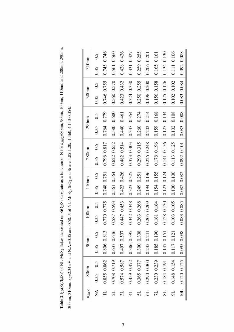
Table1
I2D (Si)/I0 (Si)ofNL
-MoS
2flakes
depositedon
SiO2 /Sisubstrate
asa
functionofN
forhSiO
2 =80nm,90nm
,100nm,110nm
,and280nm
,290nm,
300nm,310nm
.εL =2.54
eVand
N.A
.=0.35and
0.50.nofN
L-M
oS2 ,SiO
2and
Siare5.29-1.85i,1.462,4.360-0.086i.
hSiO
280nm
90nm100nm
110nm280nm
290nm300nm
310nm
NA
0.350.5
0.350.5
0.350.5
0.350.5
0.350.5
0.350.5
0.350.5
0.350.5
1L0.686
0.6930.644
0.6490.624
0.6260.627
0.6250.627
0.6270.645
0.6360.679
0.6610.723
0.699
2L0.466
0.4740.420
0.4250.402
0.4040.409
0.4070.408
0.4070.433
0.4210.477
0.4540.537
0.505
3L0.318
0.3250.281
0.2850.268
0.2690.277
0.2750.276
0.2730.301
0.2890.346
0.3230.409
0.375
4L0.220
0.2260.192
0.1950.185
0.1850.194
0.1920.193
0.1900.216
0.2050.257
0.2360.318
0.285
5L0.156
0.1600.135
0.1370.131
0.1310.140
0.1380.139
0.1350.160
0.1490.196
0.1770.252
0.222
6L0.112
0.1160.097
0.0990.095
0.0950.104
0.1020.103
0.0990.121
0.1120.153
0.1360.203
0.175
7L0.083
0.0850.072
0.0730.071
0.0710.079
0.0770.078
0.0750.093
0.0850.121
0.1060.166
0.141
8L0.062
0.0640.054
0.0550.054
0.0540.061
0.0600.060
0.0570.073
0.0670.098
0.0850.137
0.116
9L0.048
0.0490.042
0.0430.042
0.0420.048
0.0470.047
0.0450.059
0.0530.080
0.0690.115
0.096
10L0.037
0.0380.033
0.0330.033
0.0330.039
0.0380.038
0.0360.048
0.0430.066
0.0570.098
0.081
6
Tabl
e2
I 2D
(Si)
/I0(
Si)o
fNL
-MoS
2fla
kes
depo
site
don
SiO
2/Si
subs
trat
eas
afu
nctio
nof
Nfo
rhSi
O2=
80nm
,90n
m,1
00nm
,110
nm,a
nd28
0nm
,290
nm,
300n
m,3
10nm
.εL=2
.34
eVan
dN
.A.=
0.35
and
0.50
.nof
NL
-MoS
2,Si
O2
and
Siar
e4.
85-1
.20i
,1.4
60,4
.143
-0.0
54i.
h SiO
280
nm90
nm10
0nm
110n
m28
0nm
290n
m30
0nm
310n
m
NA
0.35
0.5
0.35
0.5
0.35
0.5
0.35
0.5
0.35
0.5
0.35
0.5
0.35
0.5
0.35
0.5
1L0.
855
0.86
20.
806
0.81
30.
770
0.77
50.
748
0.75
10.
796
0.81
70.
764
0.77
90.
746
0.75
50.
745
0.74
6
2L0.
708
0.71
90.
637
0.64
60.
587
0.59
30.
561
0.56
40.
622
0.65
20.
580
0.60
00.
560
0.57
00.
561
0.56
0
3L0.
574
0.58
70.
497
0.50
70.
447
0.45
30.
423
0.42
60.
482
0.51
40.
440
0.46
10.
423
0.43
20.
428
0.42
6
4L0.
459
0.47
20.
386
0.39
50.
342
0.34
80.
323
0.32
50.
373
0.40
30.
337
0.35
40.
324
0.33
00.
331
0.32
7
5L0.
365
0.37
70.
300
0.30
80.
263
0.26
80.
249
0.25
10.
290
0.31
50.
260
0.27
40.
250
0.25
50.
259
0.25
5
6L0.
290
0.30
00.
235
0.24
10.
205
0.20
90.
194
0.19
60.
226
0.24
80.
202
0.21
40.
196
0.20
00.
206
0.20
1
7L0.
230
0.23
90.
185
0.19
00.
161
0.16
40.
154
0.15
50.
178
0.19
60.
159
0.16
80.
156
0.15
80.
165
0.16
1
8L0.
184
0.19
10.
147
0.15
10.
128
0.13
00.
123
0.12
40.
141
0.15
60.
127
0.13
40.
125
0.12
60.
134
0.13
0
9L0.
148
0.15
40.
117
0.12
10.
103
0.10
50.
100
0.10
00.
113
0.12
50.
102
0.10
80.
102
0.10
20.
111
0.10
6
10L
0.12
00.
125
0.09
50.
098
0.08
30.
085
0.08
20.
082
0.09
20.
101
0.08
30.
088
0.08
30.
084
0.09
20.
088
7

Table3
I2D (Si)/I0 (Si)ofNL
-WS
2flakes
depositedon
SiO2 /Sisubstrate
asa
functionofN
forhSiO
2 =80nm,90nm
,100nm,110nm
,and280nm
,290nm,
300nm,310nm
.εL =2.54
eVand
N.A
.=0.35and
0.50.nofN
L-W
S2 ,SiO
2and
Siare4.40-1.10i,1.462,4.360-0.086i.
hSiO
280nm
90nm100nm
110nm280nm
290nm300nm
310nm
NA
0.350.5
0.350.5
0.350.5
0.350.5
0.350.5
0.350.5
0.350.5
0.350.5
1L0.833
0.8390.791
0.7960.766
0.7690.760
0.7600.762
0.7660.769
0.7650.790
0.7790.820
0.804
2L0.679
0.6890.620
0.6270.589
0.5920.583
0.5830.585
0.5890.598
0.5910.631
0.6140.680
0.654
3L0.547
0.5580.485
0.4920.455
0.4580.453
0.4520.453
0.4560.471
0.4620.511
0.4900.569
0.538
4L0.438
0.4480.380
0.3860.354
0.3570.355
0.3540.355
0.3570.376
0.3660.418
0.3960.480
0.447
5L0.349
0.3590.299
0.3050.278
0.2800.282
0.2800.282
0.2820.303
0.2930.345
0.3240.409
0.375
6L0.279
0.2880.237
0.2420.221
0.2230.227
0.2250.226
0.2250.247
0.2370.288
0.2670.351
0.318
7L0.224
0.2320.189
0.1940.178
0.1790.184
0.1820.183
0.1820.204
0.1940.243
0.2230.304
0.271
8L0.181
0.1880.153
0.1560.144
0.1450.151
0.1490.150
0.1480.170
0.1600.207
0.1880.265
0.234
9L0.148
0.1530.124
0.1270.118
0.1190.125
0.1240.124
0.1220.143
0.1340.178
0.1600.233
0.203
10L0.121
0.1250.102
0.1040.098
0.0980.105
0.1040.104
0.1020.122
0.1130.154
0.1370.206
0.178
8

Tabl
e4
I 2D
(Si)
/I0(
Si)o
fNL
-WS 2
flake
sde
posi
ted
onSi
O2/
Sisu
bstr
ate
asa
func
tion
ofN
forh
SiO
2=80
nm,9
0nm
,100
nm,1
10nm
,and
280n
m,2
90nm
,
300n
m,3
10nm
.εL=2
.34
eVan
dN
.A.=
0.35
and
0.50
.nof
NL
-WS 2
,SiO
2an
dSi
are
4.62
-0.4
8i,1
.460
,4.1
43-0
.054
i.
h SiO
280
nm90
nm10
0nm
110n
m28
0nm
290n
m30
0nm
310n
m
NA
0.35
0.5
0.35
0.5
0.35
0.5
0.35
0.5
0.35
0.5
0.35
0.5
0.35
0.5
0.35
0.5
1L0.
970
0.97
70.
920
0.92
70.
875
0.88
20.
844
0.84
80.
907
0.93
00.
866
0.88
60.
839
0.85
30.
826
0.83
3
2L0.
908
0.92
20.
819
0.83
10.
747
0.75
70.
701
0.70
70.
798
0.83
70.
734
0.76
50.
695
0.71
50.
679
0.68
8
3L0.
824
0.84
20.
710
0.72
50.
626
0.63
80.
576
0.58
30.
686
0.73
40.
612
0.64
70.
571
0.59
20.
557
0.56
5
4L0.
728
0.74
80.
603
0.61
90.
519
0.53
00.
471
0.47
80.
578
0.62
90.
505
0.54
00.
467
0.48
70.
458
0.46
3
5L0.
629
0.65
00.
505
0.52
10.
426
0.43
70.
385
0.39
10.
482
0.53
20.
415
0.44
70.
382
0.39
90.
377
0.38
0
6L0.
535
0.55
50.
419
0.43
30.
349
0.35
90.
315
0.32
00.
399
0.44
40.
340
0.36
80.
313
0.32
70.
312
0.31
3
7L0.
450
0.46
80.
346
0.35
90.
286
0.29
40.
259
0.26
30.
328
0.36
90.
279
0.30
30.
258
0.26
90.
259
0.25
9
8L0.
376
0.39
20.
285
0.29
60.
235
0.24
20.
213
0.21
70.
271
0.30
60.
229
0.24
90.
214
0.22
20.
217
0.21
6
9L0.
313
0.32
70.
235
0.24
50.
194
0.20
00.
177
0.18
00.
223
0.25
30.
190
0.20
60.
178
0.18
40.
183
0.18
1
10L
0.26
00.
273
0.19
50.
203
0.16
10.
166
0.14
80.
150
0.18
50.
210
0.15
80.
171
0.14
90.
154
0.15
50.
153
9

Table5
I2D (Si)/I0 (Si)ofNL
-WeS
2flakes
depositedon
SiO2 /Sisubstrate
asa
functionofN
forhSiO
2 =80nm,90nm
,100nm,110nm
,and280nm
,290nm,
300nm,310nm
.εL =2.54
eVand
N.A
.=0.35and
0.50.nofN
L-W
eS2 ,SiO
2and
Siare4.22-1.86i,1.462,4.360-0.086i.
hSiO
280nm
90nm100nm
110nm280nm
290nm300nm
310nm
NA
0.350.5
0.350.5
0.350.5
0.350.5
0.350.5
0.350.5
0.350.5
0.350.5
1L0.728
0.7330.700
0.7030.690
0.6900.698
0.6950.697
0.6940.717
0.7070.748
0.7320.786
0.766
2L0.533
0.5390.498
0.5020.489
0.4890.501
0.4980.499
0.4950.528
0.5130.572
0.5490.628
0.598
3L0.394
0.4000.362
0.3650.354
0.3550.369
0.3650.367
0.3620.398
0.3820.446
0.4210.510
0.476
4L0.295
0.3000.268
0.2710.263
0.2630.278
0.2750.276
0.2700.306
0.2910.354
0.3290.419
0.384
5L0.223
0.2280.202
0.2040.199
0.1990.214
0.2100.211
0.2060.240
0.2260.285
0.2620.349
0.315
6L0.172
0.1760.155
0.1570.154
0.1530.167
0.1640.165
0.1600.191
0.1780.233
0.2110.294
0.261
7L0.134
0.1370.120
0.1220.121
0.1200.133
0.1300.131
0.1260.154
0.1430.193
0.1730.250
0.219
8L0.106
0.1090.095
0.0960.096
0.0960.107
0.1050.105
0.1010.126
0.1160.162
0.1430.215
0.186
9L0.085
0.0870.076
0.0770.078
0.0770.088
0.0860.086
0.0820.105
0.0960.137
0.1200.186
0.159
10L0.068
0.0700.062
0.0630.063
0.0630.073
0.0710.071
0.0680.088
0.0800.117
0.1020.162
0.138
10

Tabl
e6
I 2D
(Si)
/I0(
Si)o
fNL
-WeS
2fla
kes
depo
site
don
SiO
2/Si
subs
trat
eas
afu
nctio
nof
Nfo
rhSi
O2=
80nm
,90n
m,1
00nm
,110
nm,a
nd28
0nm
,290
nm,
300n
m,3
10nm
.εL=2
.34
eVan
dN
.A.=
0.35
and
0.50
.nof
NL
-WeS
2,Si
O2
and
Siar
e4.
64-1
.40i
,1.4
60,4
.143
-0.0
54i.
h SiO
280
nm90
nm10
0nm
110n
m28
0nm
290n
m30
0nm
310n
m
NA
0.35
0.5
0.35
0.5
0.35
0.5
0.35
0.5
0.35
0.5
0.35
0.5
0.35
0.5
0.35
0.5
1L0.
822
0.82
90.
778
0.78
40.
746
0.75
00.
729
0.73
00.
769
0.78
80.
741
0.75
40.
728
0.73
50.
731
0.72
9
2L0.
660
0.67
00.
598
0.60
60.
556
0.56
10.
536
0.53
80.
586
0.61
20.
550
0.56
70.
537
0.54
40.
543
0.54
0
3L0.
523
0.53
40.
457
0.46
60.
417
0.42
20.
400
0.40
10.
446
0.47
20.
412
0.42
80.
401
0.40
70.
410
0.40
6
4L0.
412
0.42
20.
351
0.35
80.
315
0.32
00.
302
0.30
40.
341
0.36
50.
312
0.32
60.
304
0.30
80.
315
0.31
0
5L0.
323
0.33
30.
270
0.27
70.
241
0.24
50.
232
0.23
30.
262
0.28
30.
239
0.25
00.
234
0.23
70.
246
0.24
0
6L0.
255
0.26
30.
210
0.21
60.
187
0.19
00.
181
0.18
10.
204
0.22
10.
185
0.19
40.
183
0.18
50.
195
0.18
9
7L0.
202
0.20
90.
165
0.17
00.
147
0.14
90.
143
0.14
30.
160
0.17
40.
146
0.15
30.
145
0.14
60.
156
0.15
1
8L0.
161
0.16
70.
131
0.13
50.
116
0.11
80.
114
0.11
40.
127
0.13
90.
116
0.12
20.
116
0.11
70.
127
0.12
2
9L0.
129
0.13
40.
105
0.10
80.
094
0.09
50.
092
0.09
20.
102
0.11
10.
093
0.09
80.
095
0.09
40.
105
0.10
0
10L
0.10
50.
109
0.08
50.
088
0.07
60.
077
0.07
60.
076
0.08
20.
090
0.07
60.
080
0.07
80.
077
0.08
70.
082
11

Table7
I2D (Si)/I0 (Si)ofNL
Gflakes
depositedon
SiO2 /Sisubstrate
asa
functionofN
forhSiO
2 =80nm,90nm
,100nm,110nm
,and280nm
,290nm,300nm
,
310nm.ε
L =2.34eV
andN
.A.=0.35
and0.50.n
ofNL
G,SiO
2and
Siare2.725-1.366i,1.460,4.143-0.054i.
hSiO
280nm
90nm100nm
110nm280nm
290nm300nm
310nm
NA
0.350.5
0.350.5
0.350.5
0.350.5
0.350.5
0.350.5
0.350.5
0.350.5
1L0.938
0.9390.929
0.9300.924
0.9240.923
0.9230.927
0.9310.924
0.9260.924
0.9240.928
0.926
2L0.879
0.8820.863
0.8660.854
0.8560.853
0.8530.861
0.8680.854
0.8580.855
0.8550.863
0.859
3L0.824
0.8280.803
0.8060.791
0.7930.790
0.7900.800
0.8090.791
0.7960.792
0.7920.803
0.798
4L0.773
0.7780.748
0.7510.733
0.7350.732
0.7320.744
0.7550.733
0.7390.735
0.7350.749
0.742
5L0.726
0.7310.696
0.7010.681
0.6830.680
0.6790.692
0.7040.680
0.6870.683
0.6820.699
0.691
6L0.681
0.6870.649
0.6540.632
0.6350.632
0.6310.644
0.6580.632
0.6390.636
0.6350.653
0.645
7L0.639
0.6460.606
0.6110.588
0.5910.588
0.5880.601
0.6150.588
0.5950.592
0.5910.611
0.602
8L0.600
0.6070.565
0.5710.548
0.5510.548
0.5480.561
0.5750.548
0.5550.553
0.5510.573
0.563
9L0.564
0.5710.528
0.5340.511
0.5130.511
0.5110.523
0.5390.511
0.5180.516
0.5150.538
0.527
10L0.530
0.5380.494
0.5000.477
0.4790.478
0.4770.489
0.5040.477
0.4840.483
0.4810.505
0.494
11L0.499
0.5060.463
0.4680.445
0.4480.447
0.4460.458
0.4730.446
0.4530.452
0.4500.475
0.464
12L0.469
0.4770.433
0.4390.417
0.4190.418
0.4180.429
0.4440.417
0.4240.424
0.4220.447
0.436
13L0.442
0.4490.406
0.4120.390
0.3930.392
0.3920.402
0.4170.391
0.3970.398
0.3950.421
0.410
14L0.416
0.4230.381
0.3860.366
0.3680.368
0.3680.377
0.3910.367
0.3730.374
0.3710.398
0.386
15L0.392
0.3990.358
0.3630.343
0.3450.346
0.3460.354
0.3680.344
0.3500.352
0.3490.376
0.364
12

Tabl
e8
I 2D
(Si)
/I0(
Si)o
fNL
Gfla
kes
depo
site
don
SiO
2/Si
subs
trat
eas
afu
nctio
nof
Nfo
rhSi
O2=8
0nm
,90n
m,1
00nm
,110
nm,a
nd28
0nm
,290
nm,3
00nm
,
310n
m.ε
L=1
.96
eVan
dN
.A.=
0.35
and
0.50
.nof
NL
G,S
iO2
and
Siar
e2.
819-
1.45
0i,1
.457
,3.8
79-0
.021
i.
h SiO
280
nm90
nm10
0nm
110n
m28
0nm
290n
m30
0nm
310n
m
NA
0.35
0.5
0.35
0.5
0.35
0.5
0.35
0.5
0.35
0.5
0.35
0.5
0.35
0.5
0.35
0.5
1L0.
955
0.95
70.
948
0.94
90.
940
0.94
20.
935
0.93
60.
972
0.97
50.
966
0.96
90.
959
0.96
30.
951
0.95
5
2L0.
913
0.91
50.
898
0.90
00.
885
0.88
70.
874
0.87
60.
945
0.95
00.
933
0.93
90.
919
0.92
60.
904
0.91
2
3L0.
872
0.87
50.
851
0.85
40.
832
0.83
60.
818
0.82
10.
918
0.92
50.
901
0.91
00.
881
0.89
10.
860
0.87
1
4L0.
832
0.83
60.
806
0.81
10.
783
0.78
80.
766
0.77
00.
892
0.90
10.
869
0.88
10.
844
0.85
70.
818
0.83
2
5L0.
794
0.79
90.
764
0.76
90.
738
0.74
20.
718
0.72
20.
866
0.87
70.
838
0.85
20.
808
0.82
40.
777
0.79
4
6L0.
758
0.76
40.
724
0.73
00.
695
0.70
00.
674
0.67
80.
840
0.85
30.
808
0.82
40.
773
0.79
20.
739
0.75
8
7L0.
723
0.73
00.
686
0.69
20.
655
0.66
10.
632
0.63
70.
815
0.83
00.
779
0.79
70.
740
0.76
10.
702
0.72
3
8L0.
690
0.69
70.
650
0.65
70.
617
0.62
30.
594
0.59
80.
790
0.80
70.
751
0.77
10.
709
0.73
10.
668
0.69
0
9L0.
658
0.66
60.
617
0.62
40.
582
0.58
90.
558
0.56
30.
766
0.78
40.
723
0.74
50.
678
0.70
20.
635
0.65
8
10L
0.62
80.
636
0.58
50.
592
0.55
00.
556
0.52
50.
530
0.74
30.
762
0.69
70.
720
0.64
90.
674
0.60
40.
628
11L
0.59
90.
607
0.55
50.
562
0.51
90.
525
0.49
40.
499
0.72
00.
740
0.67
10.
696
0.62
10.
647
0.57
40.
600
12L
0.57
20.
580
0.52
60.
534
0.49
00.
497
0.46
60.
470
0.69
70.
719
0.64
60.
672
0.59
40.
621
0.54
60.
572
13L
0.54
60.
554
0.50
00.
507
0.46
30.
470
0.43
90.
444
0.67
50.
698
0.62
20.
649
0.56
90.
596
0.52
00.
546
14L
0.52
10.
529
0.47
40.
482
0.43
80.
445
0.41
40.
419
0.65
40.
678
0.59
90.
626
0.54
40.
573
0.49
50.
521
15L
0.49
70.
506
0.45
00.
458
0.41
40.
421
0.39
10.
395
0.63
30.
658
0.57
60.
605
0.52
10.
550
0.47
10.
498
13

References
[1] Y. Y. Wang, Z. H. Ni, Z. X. Shen, H. M. Wang and Y. H. Wu, Appl. Phys. Lett., 2008, 92, 043121.[2] D. Yoon, H. Moon, Y.-W. Son, J. S. Choi, B. H. Park, Y. H. Cha, Y. D. Kim and H. Cheong, Phys. Rev.
B, 2009, 80, 125422.[3] Y. K. Koh, M.-H. Bae, D. G. Cahill, E. Pop, ACS Nano, 2011, 5, 269.[4] S.-L. Li, H. Miyazaki, H. Song, H. Kuramochi, S. Nakaharai and K. Tsukagoshi, ACS Nano, 2012, 6,
7381.[5] C. Casiraghi, A. Hartschuh, E. Lidorikis, H. Qian, H. Harutyunyan, T. Gokus, K. S. Novoselov, A. C.
Ferrari, Nano Letters, 2007, 7, 2711.[6] W. P. Han, Y. M. Shi, X. L. Li, S. Q. Luo, Y. Lu and P. H. Tan, Acta Phys. Sin., 2013, 62, 110702.[7] V. G. Kravets, A. N. Grigorenko, R. R. Nair, P. Blake, S. Anissimova, K. S. Novoselov, A. K. Geim, Phys.
Rev. B, 2010, 81, 155413.[8] X. L. Li, X. F. Qiao, W. P. Han, Y. Lu, Q. H. Tan, X. L. Liu, P. H. Tan, Nanoscale, 2015, 7, 8135.
14