devefopment os au rd aug - defense technical · pdf fileenhanced transistor properties will be...
TRANSCRIPT
Rfesearchi &
IAD-A253 930 Devefopment
DTICELECTE
RD AUG 12 1992Os AUSemiconductor-Metal EutecticComposites for High PowerSwitching
I Final Report
Q. NguyenP. RossoniI M. LevinsonB.M. Ditchek
I Research supported by the SDIO Innovative Scienceand Technology Office and managed by ONR underI Contract No. N00014-86-C-0595
1 ThIS document hs been approvedlt? public zelease aind sale; itsdilstzibutiOn is unlimJited.
GTE Laboratories Incorporated40 Sylvan Road
Waltham, MA 02254
92 7 its II is1 \\U \Ul\fI\\\

TABLE OF CONTENTS
Section Page
1 Introduction 1
2 SME Transistors 32.1 SME Transistor Fabrication 32.2 Transistor Properties - DC Operation 4
2.1.1 Blocking Voltage 52.2.2 Saturation Current 72.2.3 Series Resistance 9
2.3 Transistor Properties - Pulse Tests 92.4 SME Transistor Modeling 13
2.4.1 Model for Breakdown Voltage 132.4.2 Model for Transients 142.4.3 Model for Optimized Performance 15
2.5 SME Device Assessment 16
3 Materials and Microstructural Issues in SME Devices 193.1 The Effect of Crystal Growth 193.2 The Effect of Materials System 21
4 Implications for Pulsed Power Applications and Summary 23
5 References 'eo25I Accesion ForAppendix A: Final Report April 1990 NTIS CRA&I
OTIC IA, f 7ApedxU;', mno ;.ced La
Appendix B: Recent publications Jjisitication .
IBy....... B y ........... ........ ........... ..... ...
Oit,'butionq I
DistI I 'J A
,
:,-
...
.
Statement A per telecon Gabriel RoyCode 1112Arlington, VA 22217-5000
SNW 8/10/92
M~C QtTLrN ZSMy

LIST OF FIGURES
Figure Page
1 SME transistor geometry. 4
2 Characteristics of a Si-TaSi2 SME transistor. 4
3 Transfer characteristics of a 2.2 kV SME transistor. 5
4 DC breakdown voltage vs wafer thickness. 6
5 Oval structure for high-current devices. 7
6 Transfer characteristics of a parallel device. 8
7 Circuit diagrams employed to pulse test SME devices. 10
8 Voltage waveform of a SME device and a conventional MOSFET 11in a 1200 V test.
9 Voltage waveforms of a SME transistor under pulsed test. The solid line shows 11
a full 6 kV waveform supported by the device. Above 6 kV, the devicebreaks down, as shown by the dashed line.
10 Breakdown voltage vs wafer thickness in pulse test. 12
11 A voltage and current pulse generated with the inductive circuit using a SME 12transistor.
12 Current waveform at switch opening portion in Figure 11 with the time 13scale expansion.
13 Simulated SME transistor turn-on response for different Vd. 14
14 VLcv vs interrod spacing, s, for different s/r ratios. 15
15 Optimum areal conductance vs breakdown voltage for conventional devices 16and SME devices with two combinations of junction radii and spacing.
16 Specific resistance vs breakdown voltage for SME devices and MOSFETS. 17Theoretical expectations based on the unipolar limit have also been shown.
17 Counts of TaSi2 rods in 85 pin square frame vs position for wafers grown 20with seed and crucible rotation of (a) (±6) rpm and (b) (0, 12) rpm,respectively.
18 Breakdown voltage as a function of position in a wafer for wafers cut from 20crystals grown at different conditions.
19 Scanning electron micrograph of the GaAs-GdAs eutectic grown by the 22Bridgman technique.

LIST OF TABLES
Table Page
1 Sample data for various SME devices. 8
2 Comparison of SME devices with other high-power devices. 18
iii

1. INTRODUCTION
This report reviews the accomplishments of a research program that sought to develop a totallynew material for high-power transistor switching. The material, which we have generally referredto as SME for semiconductor-metal eutectic, is a composite with a high density of aligned,micron-sized metallic rods embedded in a matrix of a semiconductor. This material differsdramatically from silicon, the material used to fabricate almost all other conventional high-powertransistors. Silicon is a single-phase pure material. Devices are fabricated from this materialthrough the use of thin-film techniques to incorporate junctions in the surface which enableswitching. The composite material contains internal junctions throughout the bulk of the material.Further, it consists of a two-phase equilibrium structure, which because of concerns for defects inthe semiconductor, has never before been demonstrated to be of electronic quality, that is,suitable for the fabrication of high-quality devices like high-voltage transistors.
The initial goal for this program was to be the first to take a particular two-phase composite SMEmaterial, consisting of a silicon matrix and tantalum disilicide metallic rods, and demonstratethat it could be made into a bulk transistor that utilized the Schottky junction at the interfacebetween the semiconductor and metal phases to pinch off the channels within the semiconductormatrix. Within the first three years of the program, this was accomplished with the demonstrationof a device that blocked 1 kV, a high value for a silicon device.! The program was renewed for amore developmental phase with the goal of demonstrating a 50 A, 10 kV switch within the nextthree years, a combination of properties that has never been achieved for a silicon-based transistor,despite the many years of development on conventional silicon transistor devices. This programwas well on the way to demonstrating such a goal, when circumstances associated with internalGTE affairs caused the premature termination of the program approximately 15 months early.Within the allotted period, the critical interim goals of 6 kV blocking voltage and the ability toparallel devices for higher current were clearly demonstrated.2
The purpose of this report is to summarize accomplishments and the state-of-the-art in SMEdevices as well as to try to build some excitement regarding this technology so that its uniqueconcept and approach are not abandoned simply because of GTE's exit from this developmenteffort. The potential of this approach is sufficiently high and the concept sufficiently unique thatfurther evaluation and testing should be performed.
Section 2 will review SME transistor fabrication techniques and dc and pulsed properties. Modelinghas been used extensively in this program to develop an understanding of the unusual propertiesof these devices, and this will be reviewed in this section for direct comparison with experimentalresults. This section will close with a comparison of the SME device performance with theperformance of three other terminal devices, like the SIT and the MOSFET. Section 3 willaddress the materials aspects of these devices. It will show how microstructures features likesize, interrod spacing, the distribution of interrod spacing, and rod divergence affect device prop-

erties. The state-of-the-art of materials development for these applications will be reviewed, and
based on experimental and modeling results, the potential for advanced materials to generate
enhanced transistor properties will be evaluated. Finally, Section 4 will assess the implications of
SME transistors for pulsed power applications and will summarize and make recommendations
for future work. The f'mal report submitted to ONR at the conclusion of the first three years of
the program is included in the Appendix. It includes details that may serve as a useful referencefor the new data included in this report. Recent publications are also included in the Appendix.
2

2. SME TRANSISTORS
The operation of an SME transistor is schematically shown in Figure 1. Current flowing from asource to a drain must pass through a gate. Reverse biasing this gate can expand the depletionzone around the rods under the gate and pinch off the current channels. Although a broaddiscussion of microstructure effects will be reserved for the next section, it is necessary to makeseveral points regarding the material at this point to help the reader understand basic transistorproperties. First, for the benchmark material in which we have made all transistors, the Si-TaSi,the rod density is about 1.6 x 10' rods/cm2. Average interrod spacing is about 7 jim, and thediameter of a typical rod is 1 tm. The rod distribution is not regular, as a lithographicallydeposited structure would be. Rather the rods appear to distribute themselves in the walls of anirregularly shaped cell. Thus current moving from the source to the drain must move around therods, creating an elongated, twisted path and a higher resistance than would be expected basedonly on tho dimensions and the carrier concentration of the semiconductor matrix. The actualarrangement of the rods is different in the bulk of the material relative to the surface due to slightmisalignment of the rods. Maximum divergence of the rods relative to the normal surface hasbeen measured to be 60. This has been found to be an important defect that alters the blockingvoltage properties of the SME transistor.
2.1. SME Transistor Fabrication
SME transistor fabrication really starts with the crystal growth process. Si and Ta are placed in acrucible in a ratio that establishes the net composition as that of the eutectic between Si andTaSi. The crucible is heated to the eutectic temperature, approximately 1400*C, then contactedon the melt surface with a single crystalline Si seed. In our case, a Si crystal with a (111)orientation was most frequently used for the seed. After equilibration, the seed is raised at a fixedrate, approximately 20 cm/hr, resulting in the pulling of a SME crystal with the microstructurediscussed above. Crystals grown this way generally have a Si matrix carrier concentration between1 and 3 x 101 cm-3. The crystal is then oriented, sliced into (111) wafers, and suface polished.After this step, the wafers are ready for processing into devices.
Figure 1 also shows the concentric ring design used for the source, gate, and drain contacts oftest devices. Fabrication of the device started with oxidation of the SME wafer. Oxidation rateswere found to be essentially the same as for Si. The gate contact was produced in vias in theoxide. A cobalt disilicide film was used that forms a Schottky contact to the Si and an ohmiccontact to the rods. In certain cases, the gate film was implanted with B to create a p/n junction atthe interface with the matrix Si to minimize leakage. The source and drain ohmic contacts werefabricated similarly only substituting an As implant for the B to generate a n- contact and a goodohmic contact to the n-type Si matrix.
3
2.2. Transistor Properties - DC Operation
The typical transfer characteristic of a semiconductor-metal eutectic transistor is shown in Figure2. The basic characteristics of the device are similar to those of a conventional metal-semiconductorfield effect transistor, or MESFET. Both display a linear region at low voltage, determined by theseries resistance, and a saturation region. For a power device, the linear region should be as steepas possible (that is, resistance should be small), the saturation current should be large, and themaximum drain voltage, indicative of the maximum voltage the device will hold-off, should alsobe high.
Source Gate Junctions Drain
Si Matrix TaSi 2 Fibers
Figure 1. SME transistor geometry.
Per Vert.Division 5 mA
Per Horiz.DMslIon 20 V
Per Step 2 V
gm PerDivision 2.5 mS
Figure 2. Characteristics of a Si-TaSi2 SME transistor.
4
Over the course of this program, the factors that affect these parameters, the initial slope, thesaturation current, and the maximum blocking voltage of SME devices, have been evaluated indetail. Empirical studies included correlation of device properties with variations in the spacingsof the device dimensions, including gate-to-drain spacings and wafer thickness, changes in thedevice geometry from a concentric ring to a more conventional rectangular design, and materialcharacteristics, such as resistivity. Results from these studies will be presented in this section.With the hopes of achieving clarity, the data will be presented in separate sections on blockingvoltage, saturation current, and series resistance. All data presented were taken from dc tests ofthe transistors on either a Textronix 571 or a Sony/Textronix high-power curve tracer. Pulsedmeasurements will be presented in the following section.
2.2.1. Blocking Voltage
The highest blocking voltage achieved in a SME device on a dc test to date is 2.2 kV. A curvetrace for this device is shown in Figure 3. This high blocking voltage is remarkable when oneconsiders that the maximum breakdown voltage expected for a conventional Si device with acomparable carrier concentration of 1015 cm -3 is only 0.3 kV based on an avalanche breakdownmechanism.3 The observed breakdown voltage of SME devices is unusual, in that it does notdepend on the carrier concentration (at least within this range), but rather depends on twogeometric factors, the gate-to-drain distance ind the wafer thickness, as well as temperature andheating effects.
Figure 3. Transfer characteristics of a 2.2 kV SME transistor.
5
Figure 4 shows how wafer thickness and gate-to-drain distance affect the blocking voltage. Thegraph shows data on devices from several wafers that were first tested at a 10 mil thickness, thenreduced in thickness from the backside by either a polishing or etching step, and retested. Thiswas continued until wafer thickness was about 2 mils. The data on devices with 137 gm gate-to-drain distances was data previously reported in the report dated April 1990 (in Appendix A). Thelarger spacings used since that time were chosen to achieve higher breakdown voltages. Asshown for the 500 gm gate-to-drain spacing data, higher voltages were achieved. However, thedesired voltages were not observed until wafer thicknesses were reduced to only 2 mils.
1800 . . . . .. .. ...
1400 500 gm Gate-to-DrainDistance
o 1000
m 600137 pgm Gate-to-Drain 1-.C Distance -
200 L - . . .04 8 12Wafer Thickness (mils)
Figure 4. DC breakdown voltage vs wafer thickness.
The effects of wafer thickness and gate-to-drain distance shown in Figure 4 have been consistentlyobserved in all samples. The maximum blocking voltage is predictably about 40 kV/cm multipliedby the gate-to-drain distance in thin wafers (the multiplier is higher in pulsed tests, as will beseen in Section 2.3). Both effects have been explained in terms of the divergence of the floatingjunctions and their effect on the "effective" gate-to-drain distance. The models used to explainthe results will be discussed in great detail in Section 2.4.
For the device shown in Figure 3, the saturation current exceeds 30 mA. With the high voltagesinvolved and the long times required to achieve the curve trace (approximately 17 ms), thedevice under test can get hot. Heating during the period of transistor testing can affect leakagecurrents and give a false indication of breakdown even before avalanching can occur. Thus thedata in Figure 4 can be partially affected by thermally induced leakage. Nevertheless, it is clearthat the trend of increased breakdown with reduced thickness or increased gate-to-drain distanceis certain, as it has been substantiated with pulses too short to enable heating, about 1 gs.
6
2.2.2. Saturation Current
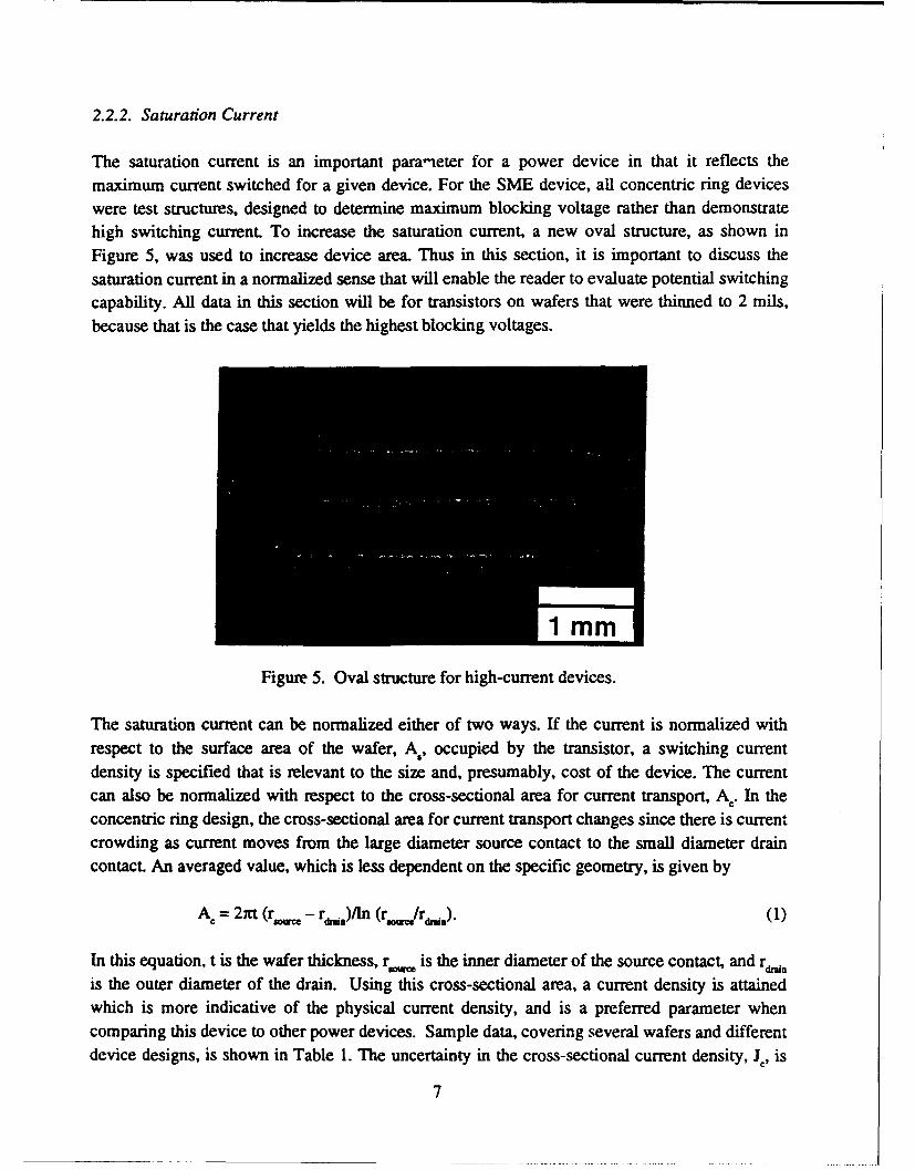
The saturation current is an important para'aeter for a power device in that it reflects themaximum current switched for a given device. For the SME device, all concentric ring deviceswere test structures, designed to determine maximum blocking voltage rather than demonstratehigh switching current. To increase the saturation current, a new oval structure, as shown inFigure 5, was used to increase device area. Thus in this section, it is important to discuss thesaturation current in a normalized sense that will enable the reader to evaluate potential switchingcapability. All data in this section will be for transistors on wafers that were thinned to 2 mils,because that is the case that yields the highest blocking voltages.
1 MM
Figure 5. Oval structure for high-current devices.
The saturation current can be normalized either of two ways. If the current is normalized withrespect to the surface area of the wafer, A, occupied by the transistor, a switching currentdensity is specified that is relevant to the size and, presumably, cost of the device. The currentcan also be normalized with respect to the cross-sectional area for current transport, Ac. In theconcentric ring design, the cross-sectional area for current transport changes since there is currentcrowding as current moves from the large diameter source contact to the small diameter draincontact. An averaged value, which is less dependent on the specific geometry, is given by
At = 2nt (ro,, - rdm,)/ln (,! ) 1
In this equation, t is the wafer thickness, ; is the inner diameter of the source contact, and r.. *
is the outer diameter of the drain. Using this cross-sectional area, a current density is attainedwhich is more indicative of the physical current density, and is a preferred parameter whencomparing this device to other power devices. Sample data, covering several wafers and differentdevice designs, is shown in Table 1. The uncertainty in the cross-sectional current density, JC, is
7
larger than in the surface area current density, J, because of a substantial uncertainty in the wafer
thickness of about ± 25%. Surface current densities range from 0.36 A/cm2 to 1.2 A/cm2 , andcross-sectional current densities range from 15 to 26 A/cm2. The saturation currents are consideredrepresentative and typical, but it should be noted that even in a given wafer, considerablevariability in I. is observed.
Table 1. Sample Data for Various SME Devices
G-D Distance r I R J,
Device No. (gim) (Q2-cm) (mA) (f2) (A/cm 2) (A/cm 2)
85-5 N11 500 46 30 5000 1.21 26
85-29 H9 1000 31 25 1667 0.36 15
70-24 C16 (Oval) 500 17 77 172 0.98 19
The table shows that increasing the gate-to-drain distance to achieve high voltage adverselyaffects the switchable current per unit surface area of the wafer but does not substantially lowerthe current normalized to the cross-sectional area. Although the surface area normalized currentsmay be considered low, the cross-sectional current density is high. This will be discussed furtherin Section 2.5.
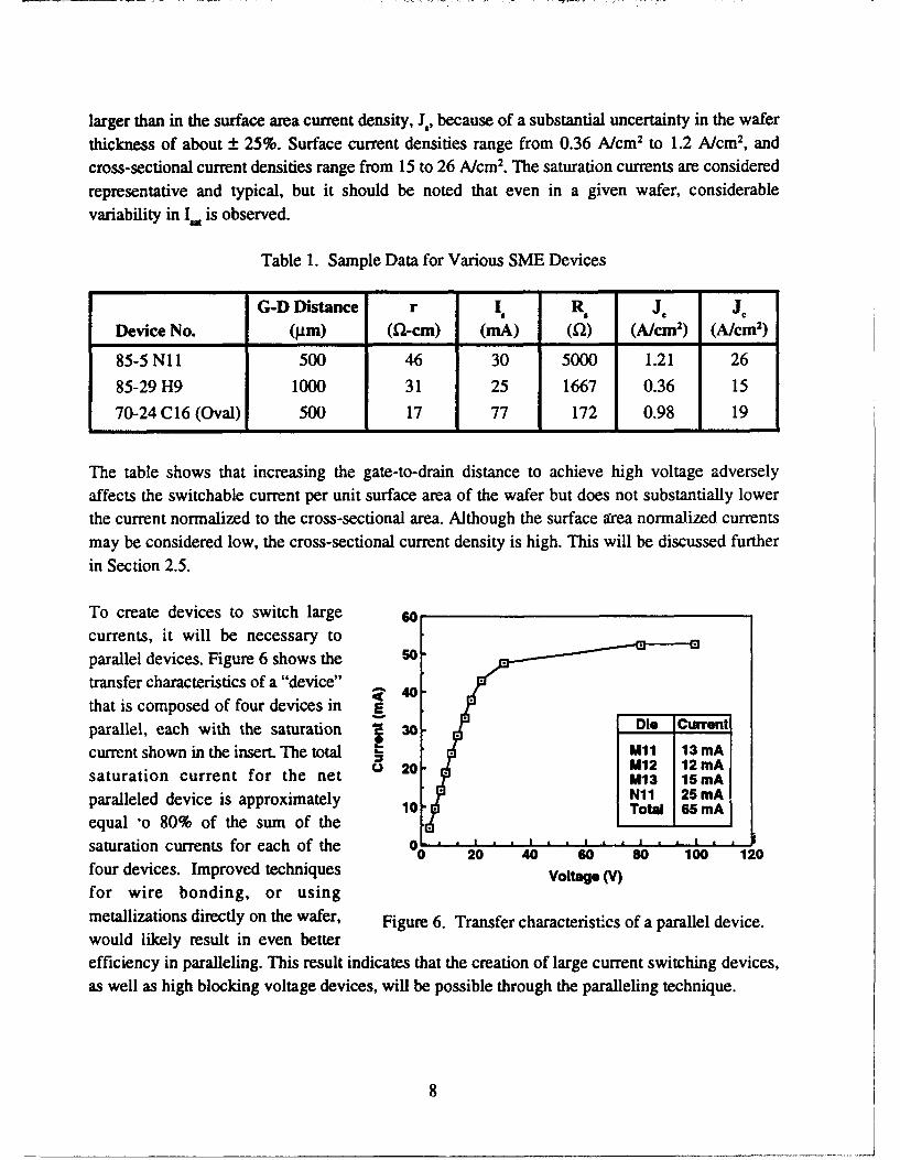
To create devices to switch large 60
currents, it will be necessary toparallel devices. Figure 6 shows the s" '
transfer characteristics of a "device" 40
that is composed of four devices inparallel, each with the saturation 30 ulcurrent shown in the insert. The total Mll 13 mA
saturation current for the net M13 15mAparalleled device is approximately 10 N T 5mA
equal *o 80% of the sum of thesaturation currents for each of the t' ' 10'0 120
Oi 20 40 0 8 10 12
four devices. Improved techniques Voltage (V)for wire bonding, or usingmetallizations directly on the wafer, Figure 6. Transfer characteristics of a parallel device.would likely result in even betterefficiency in paralleling. This result indicates that the creation of large current switching devices,as well as high blocking voltage devices, will be possible through the paralleling technique.
8

2.2.3. Series Resistance
Table 1 also shows the series resistance for each device, calculated as the ratio of 50 mV with thedrain current at 50 mV. This may be compared with the expected resistance based on theresistivity measured for the particular wafer and the "effective" cross-sectional area and length of
transport. When the comparison is made for these 50 gim thick devices, agreement is excellent,indicating that the contacts are good and that the entire thickness is being utilized as the currentchannel.
As a result of the relatively high resistivity of these wafers (good devices require a resistivityexceeding 10 to 15 Q-cm), the long gate-to-drain distances needed to achieve high voltage, andthe small size of the devices, the series resistance of these devices tends to be high. As in theIoval, large area device, small series resistance can be achieved by scaling-up the size of thedevice to achieve high currents.
12.3. Transistor Properties - Pulse Tests
The three circuits employed to pulse test SME devices are shown in Figure 7. The highestvoltage pulses were generated with the spark coil circuit shown in Figure 7(a), with either the4 kV Xenon flash coil, which generated a 700 ns pulse, or a 25 kV automotive spark coil, whichIgenerated a longer 80 its pulse. These tests were operated with the gate of the transistor shortedto the drain so that maximum saturation currents flowed through the transistor during pulsetesting. Figure 8 shows the voltage waveform in a 1200 V test for a SME device with a 500 gmgate-to-drain spacing and a conventional MOSFET rated at 500 V. The figure shows that theSME device readily supports the high-voltage pulse, but the MOSFET does not. An example of
the voltage waveform with the automotive coil is shown in Figure 9 as a 1000 gtm gate-to-draindistance device is tested. The device is clearly demonstrated to support a full 6 kV. Above 6 kV,the device breaks down, indicating that 6 kV for this device is the maximum blocking voltage.
It should be noted that all devices tested using this circuit were tested in the same probe stationused for the dc tests, but the entire wafer, including the device under test, was immersed intransformer oil. Devices not immersed in transformer oil did not support a high voltage andshowed to the observant eye a spark between metal probes contacting the device.
Figure 10 shows the results of pulse test measurements of breakdown voltage on several devices
I with different gate-to-drain distances at different wafer thicknesses. As for the dc tests, thebreakdown voltage increases as the thickness decreases, supporting the concept that the divergenceof the rods limits the breakdown voltage in thick wafers.
I9I
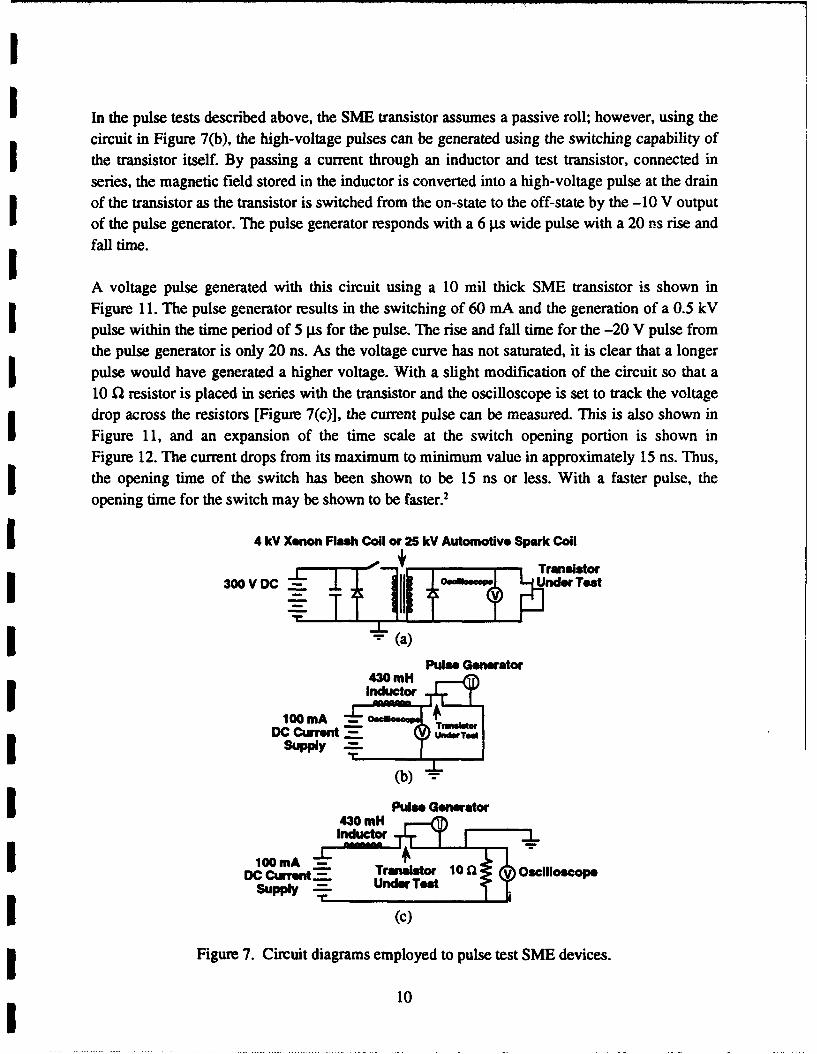
In the pulse tests described above, the SME transistor assumes a passive roll; however, using the
circuit in Figure 7(b), the high-voltage pulses can be generated using the switching capability ofthe transistor itself. By passing a current through an inductor and test transistor, connected inseries, the magnetic field stored in the inductor is converted into a high-voltage pulse at the drainof the transistor as the transistor is switched from the on-state to the off-state by the -10 V outputof the pulse generator. The pulse generator responds with a 6 pls wide pulse with a 20 ns rise andfall time.
A voltage pulse generated with this circuit using a 10 mil thick SME transistor is shown inFigure 11. The pulse generator results in the switching of 60 mA and the generation of a 0.5 kVpulse within the time period of 5 pls for the pulse. The rise and fall time for the -20 V pulse fromthe pulse generator is only 20 ns. As the voltage curve has not saturated, it is clear that a longerpulse would have generated a higher voltage. With a slight modification of the circuit so that a10 Q resistor is placed in series with the transistor and the oscilloscope is set to track the voltagedrop across the resistors [Figure 7(c)], the current pulse can be measured. This is also shown inFigure 11, and an expansion of the time scale at the switch opening portion is shown inFigure 12. The current drops from its maximum to minimum value in approximately 15 ns. Thus,
the opening time of the switch has been shown to be 15 ns or less. With a faster pulse, theopening time for the switch may be shown to be faster.?
4 kV Xenon Flash Coil or 25 kV Automotive Spark Coil
j ~300 V DC .L. li maepHUnder Test
-a)
Pulse Generator430 mH -<
100 mA -I DC Current _UndSITed
supply
(b)
430 m Pulse Generator
DC Currn-t Transistor 10 Q OscilloscopeSuppl Une o
Figure 7. Circuit diagrams employed to pulse test SME devices.
10

I
1 1.4 ...
I Eutectic
j0. 6
~~0.62~*
0.
0 0.2 0.4 0.6 0.8 1 1.2I Time (jis)
IFigure 8. Voltage waveform of a SME device and a conventional MOSFET in a 1200 V test.
I 6
I 4I 4
0 3
I0 20 40 60 80 100
rTime (is)
Figure 9. Voltage waveforms of a SME transistor under pulsed test. The solid line shows a full6 kV waveform supported by the device. Above 6 kV, the device breaks down, asshown by the dashed line.
11

4.5---------- ---
o3.5 'Best
2.5 Averageo 2
S1.5
0.5 0 2 4 6 8 10 12
Wafer Thickness (mils)
Figure 10. Breakdown voltage vs wafer thickness in pulse test.
~0.6-----------------120
0 Drain Voltage0
C 0.440
0.2 i*.4
0h.0
I' 0& I) Source Current c00 00 2 4 6 8 10
Time (jts)
Figure 11. A voltage and current pulse generated with the inductive circuit using a SMEtransistor.
12
80
E'C 40
o0
0
0 10 20 30 40 50Time (ns)
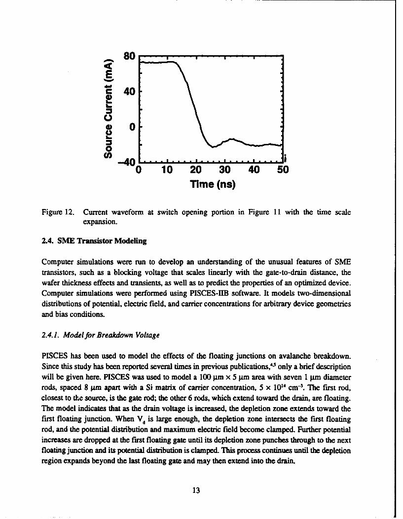
Figure 12. Current waveform at switch opening portion in Figure 11 with the time scale
expansion.
2.4. SME Transistor Modeling
Computer simulations were run to develop an understanding of the unusual features of SMEtransistors, such as a blocking voltage that scales linearly with the gate-to-drain distance, thewafer thickness effects and transients, as well as to predict the properties of an optimized device.Computer simulations were performed using PISCES-lIB software. It models two-dimensionaldistributions of potential, electric field, and carrier concentrations for arbitrary device geometriesand bias conditions.
2.4.1. Model for Breakdown Voltage
PISCES has been used to model the effects of the floating junctions on avalanche breakdown.Since this study has been reported several times in previous publications,' only a brief descriptionwill be given here. PISCES was used to model a 100 gm x 5 pm area with seven 1 pm diameterrods, spaced 8 ;Lm apart with a Si matrix of carrier concentration, 5 x 10' cm-3. The first rod,closest to the source, is the gate rod; the other 6 rods, which extend toward the drain, are floating.The model indicates that as the drain voltage is increased, the depletion zone extends toward thefirst floating junction. When Vd is large enough, the depletion zone intersects the first floatingrod, and the potential distribution and maximum electric field become clamped. Further potentialincreases are dropped at the first floating gate until its depletion zone punches through to the nextfloating junction and its potential distribution is clamped. This process continues until the depletionregion expands beyond the last floating gate and may then extend into the drain.
13

This model explains why the breakdown voltage is associated with the gate-to-drain distance andwhy avalanching is avoided even when the carrier concentration is high. Since the maximumelectric field is clamped by the floating junctions, an average electric field is in place betweenthe gate and drain contacts. In our model, the average field was about 50 kV/cm. In practice, thepulse tests have yielded about 4 kV for a 500 gtm gate-to-drain spacing, or about 80 kV/cm, and6 kV for a 1000 lun spacing, or about 60 kV/cm. DC tests have yielded slightly lower averagefields, but as we said before, these results may be limited by thermal affects.
2.4.2. Model for Transients
Transients have also been modeled using PISCES." Figure 13 shows the calculated turn-onresponse of a model device from a starting drain voltage of Vd = 50, 200, and 300 V. In eachcase, the model indicates a rapid initial current rise and then a slow tail that increases as the drainvoltage is increased. The higher the initial drain voltage, the longer the tail.
600--------- -----------I5 300V
'E 400O500
200 2100 50V
050 V
-20 0 20 40 60 80 100 120Time (lis)
Figure 13. Simulated SME transistor turn-on response for different Vd.
The physical explanation for the long tails may be as follows. During the turn-on process, thefirst carriers to transit the gate region must pass through the extended depletion zone before theycan force current at the drain. The transit time will decrease significantly as the depletion regioncollapses back toward the gate. The rate of this collapse will be determined by the gate-sourceand gate-drain capacitances. Thus the turn-on transient may be slower than the turn-off with atime constant that would increase with increasing Vd. Additionally, there is another effect associatedwith guard rings in conventional devices. The floating junctions exchange charge with the bulk
semiconductor as their potential shifts. During the turn-on process, the charging of the floatingjunctions occurs by minority carrier current or leakage and is relatively slow. During this time,the depletion zones of the floating junctions are larger than when they are neutral, thus constricting
14
the current channel and producing a long time-constant tail to the drain current during turn-on.The opposite occurs during the turn-off process as the floating junctions discharge by a majoritycarrier process. Experimental results consistent with this model have been observed.
2.4.3. Model for Optimized Performance
In this case, the model was used to answer the question, What is the ideal microstructure for
obtaining high-voltage breakdown, particularly, suppressing breakdown while achieving high
on-state conductance? The primary requirement is that the gate depletion zone must reach the
first floating junction before avalanche breakdown occurs. This condition defines the carrier
concentration, Nd, such that the maximum permissible Nd is the one that yields a depletion zone
equal to the spacing between rods, s. Higher Nd would lead to avalanche breakdown before the
field limiting capabilities of the floating gates take effect and lower Nd would result in a lower
voltage drop per unit distance and a lower conductance.
Analytically determining Nd for various microstructures characterized by s, the spacing betweenrods, and r, the radius of a rod, and using PISCES to compute I-V characteristics to obtain
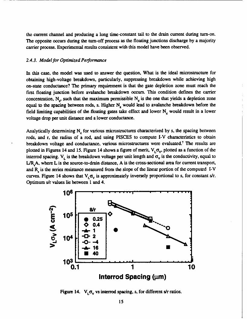
breakdown voltage and conductance, various microstructures were evaluated.7 The results areplotted in Figures 14 and 15. Figure 14 shows a figure of merit, VLav, plotted as a function of theinterrod spacing. VL is the breakdown voltage per unit length and av is the conductivity, equal toUJR,A, where L is the source-to-drain distance, A is the cross-sectional area for current transport,and R, is the series resistance measured from the slope of the linear portion of the computed I-Vcurves. Figure 14 shows that VLav is approximately inversely proportional to s, for constant sir.Optimum s/r values lie between 1 and 4.
106
i 0.2510o4 -0- 2
-0- -4> -Ar 16
* 40103 , . . ....,
0.1 1 10Interrod Spacing (jim)
Figure 14. VLa v vs interrod spacing, s, for different s/r ratios.
15
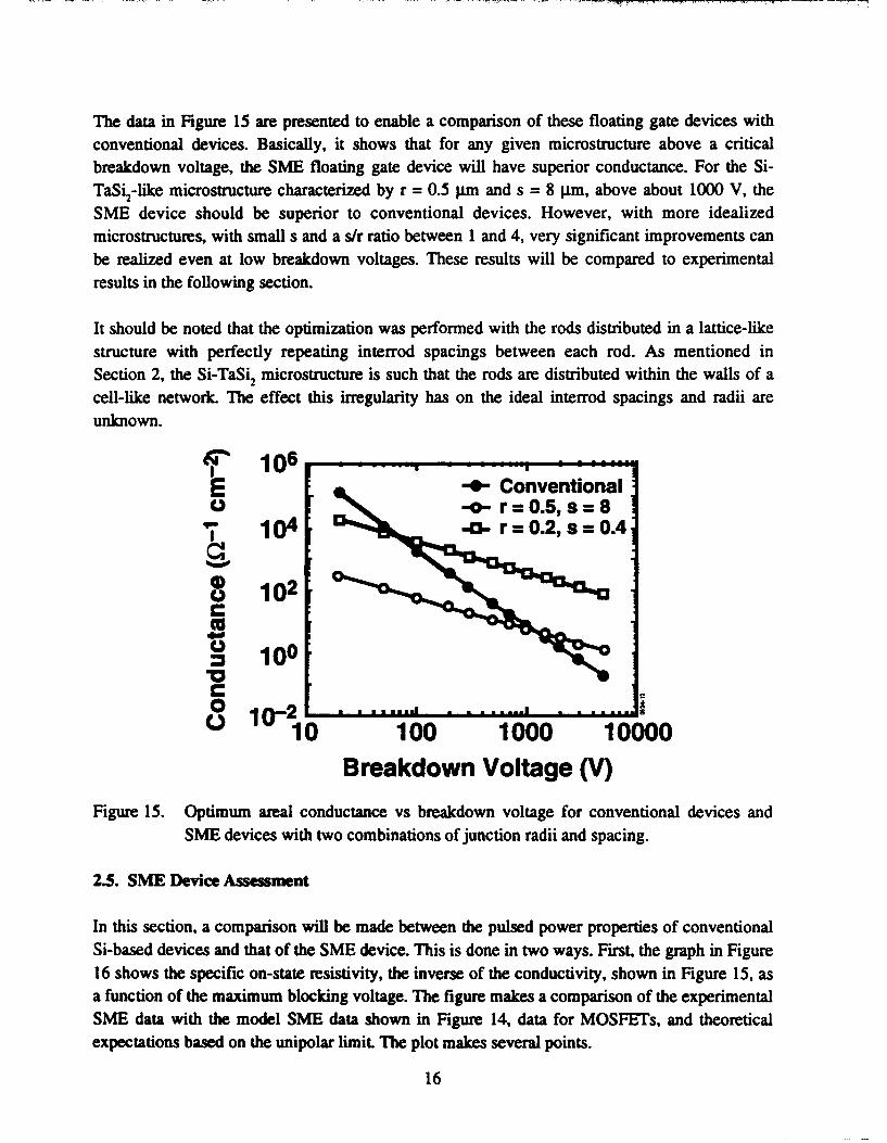
The data in Figure 15 are presented to enable a comparison of these floating gate devices withconventional devices. Basically, it shows that for any given microstructure above a criticalbreakdown voltage, the SME floating gate device will have superior conductance. For the Si-TaSi2-like microstructure characterized by r = 0.5 Jni and s = 8 im, above about 1000 V, theSME device should be superior to conventional devices. However, with more idealizedmicrostructures, with small s and a s/r ratio between 1 and 4, very significant improvements canbe realized even at low breakdown voltages. These results will be compared to experimentalresults in the following section.
It should be noted that the optimization was performed with the rods distributed in a lattice-likestructure with perfectly repeating interrod spacings between each rod. As mentioned inSection 2, the Si-TaSi 2 microstructure is such that the rods are distributed within the walls of acell-like network. The effect this irregularity has on the ideal interrod spacings and radii areunknown.
a' 106E - ConventionalT io~ -o- r=O.5,s=8" 10 4 -o3- r = 0.2, s = 0.4
o 102
0S 100
0 10-2110 100 1000 10000
Breakdown Voltage (V)
Figure 15. Optimum areal conductance vs breakdown voltage for conventional devices and
SME devices with two combinations of junction radii and spacing.
2.5. SME Device Assessment
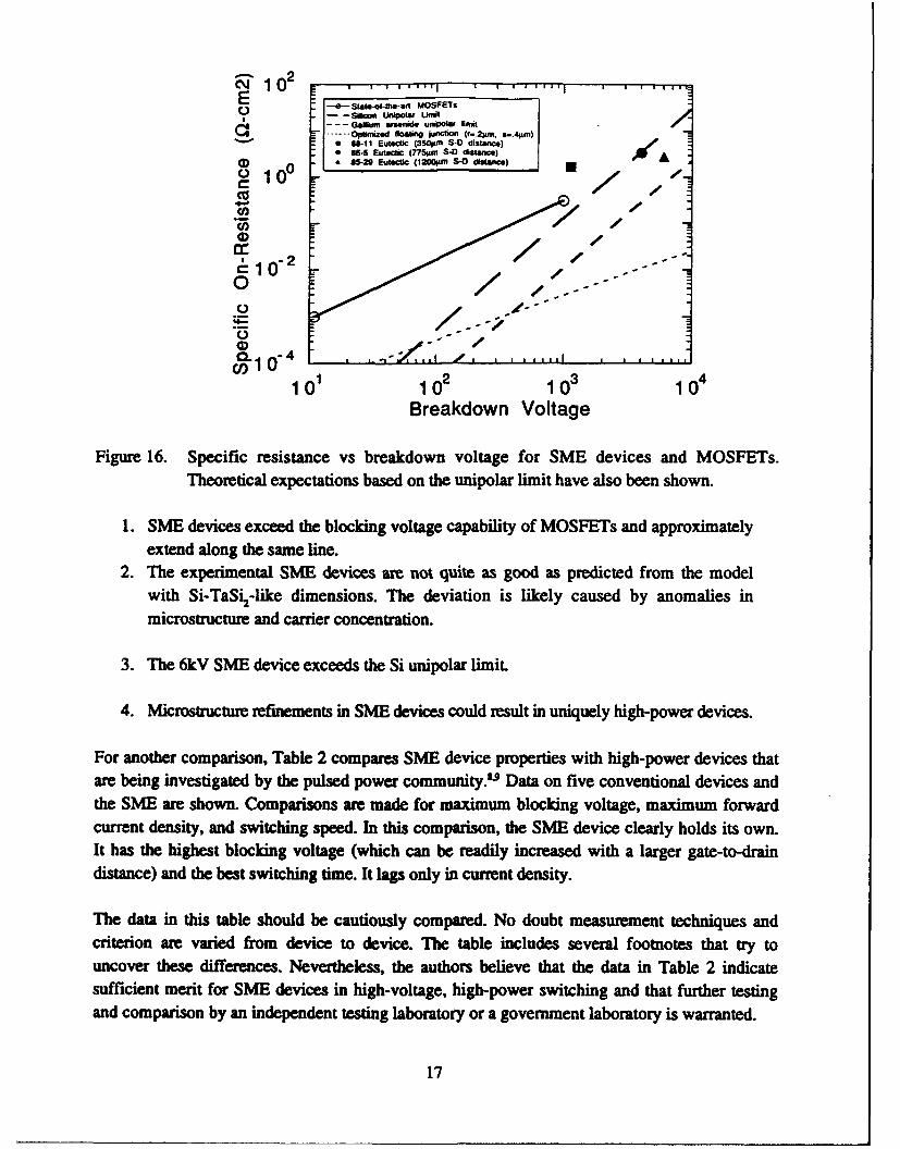
In this section, a comparison will be made between the pulsed power properties of conventionalSi-based devices and that of the SME device. This is done in two ways. First, the graph in Figure16 shows the specific on-state resistivity, the inverse of the conductivity, shown in Figure 15, asa function of the maximum blocking voltage. The figure makes a comparison of the experimentalSME data with the model SME data shown in Figure 14, data for MOSFETs, and theoreticalexpectations based on the unipolar limit. The plot makes several points.
16
E--S-- Stale-o-the-arl MOSFETs0 516000 UnkwPolaf Uwidt
--- Gam amnide unipoa kftJ----- Opmoized foating juncio0n (,-.2pm. ,..4#m)
6 66-1l Eutect (350pm S-0 ditance)* 65-5 Eutectic (775*1M S- distance) AO
0 0 85-29 Eu/1t1 (120M0 distac)
040CO)
0
101 102 10 3 1 0 4
Breakdown Voltage
Figure 16. Specific resistance vs breakdown voltage for SME devices and MOSFETs.Theoretical expectations based on the unipolar limit have also been shown.
1. SME devices exceed the blocking voltage capability of MOSFETs and approximatelyextend along the same line.
2. The experimental SME devices are not quite as good as predicted from the modelwith Si-TaSi2-like dimensions. The deviation is likely caused by anomalies inmicrostructure and carrier concentration.
3. The 6kV SME device exceeds the Si unpolar limit.
4. Microstructure refinements in SME devices could result in uniquely high-power devices.
For another comparison, Table 2 compares SME device properties with high-power devices thatare being investigated by the pulsed power community." Data on five conventional devices andthe SME are shown. Comparisons are made for maximum blocking voltage, maximum forwardcurrent density, and switching speed. In this comparison, the SME device clearly holds its own.It has the highest blocking voltage (which can be readily increased with a larger gate-to-draindistance) and the best switching time. It lags only in current density.
The data in this table should be cautiously compared. No doubt measurement techniques andcriterion are varied from device to device. The table includes several footnotes that try touncover these differences. Nevertheless, the authors believe that the data in Table 2 indicatesufficient merit for SME devices in high-voltage, high-power switching and that further testingand comparison by an independent testing laboratory or a government laboratory is warranted.
17

Table 2. Comparison of SME Devices with Other High-Power Devices
Bipolar GTO-Thyrlsto MOSFET Sr MOS-Thyristor SME
Hold-Off Voltage 500 2500 1000 500 3000 6000
Forward Current 40 100 10 10 325 26
Density (A/cm2)
Switching Speed 200 kHz 20 kHz 2 MHz 2 MHz 1 is <15 ns
Turn-Off Turn-Off
18
3. MATERIALS AND MICROSTRUCTURAL ISSUES IN SME DEVICES
Just as it is for a conventional transistor, the properties of a SME device are dependent upon thedevice processing steps, such as oxidation, metallization, etc. But since the processing of anSME device is so simple, it requires only two masks, the truly important materials processingstep is crystal growth. For an SME device, that is the step that determines the spacing betweenjunctions and the carrier concentration. Thus the question arises as to how this step can bemodified to improve devices. Also important is the SME material itself. Clearly, the Si-TaSi2system is device worthy, but are there other device worthy eutectic materials? These are some ofthe types of questions that will be addressed in this section.
3.1. The Effect of Crystal Growth
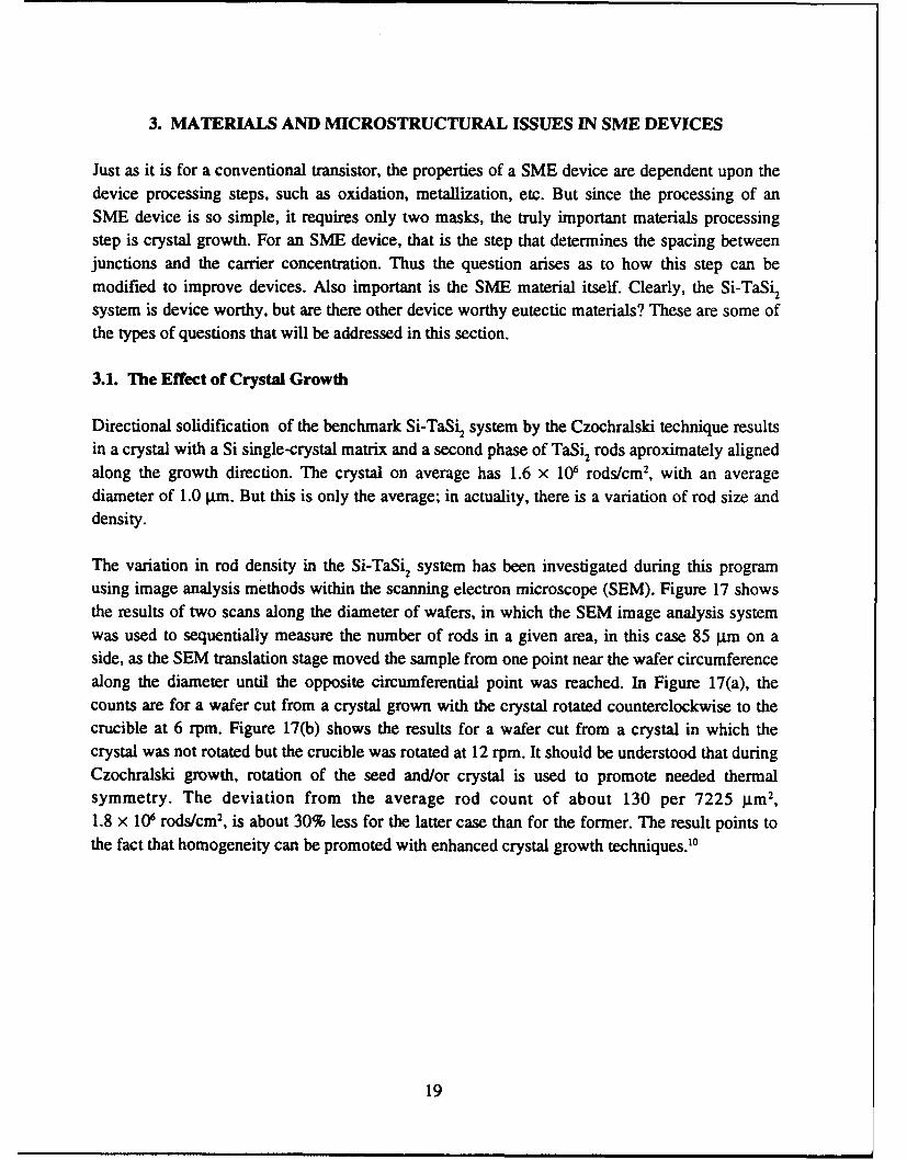
Directional solidification of the benchmark Si-TaSi2 system by the Czochralski technique resultsin a crystal with a Si single-crystal matrix and a second phase of TaSi2 rods aproximately alignedalong the growth direction. The crystal on average has 1.6 x 10⁶ rods/cm2, with an averagediameter of 1.0 im. But this is only the average; in actuality, there is a variation of rod size anddensity.
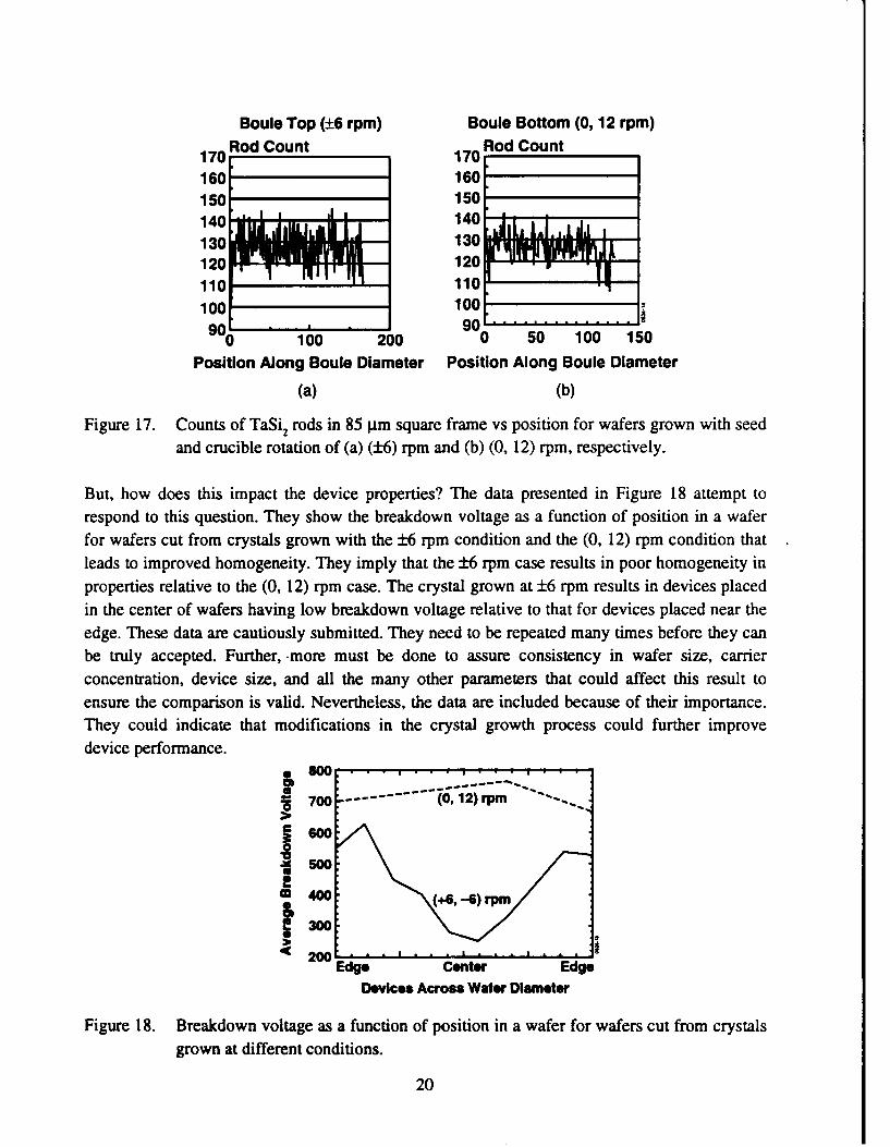
The variation in rod density in the Si-TaSi 2 system has been investigated during this programusing image analysis methods within the scanning electron microscope (SEM). Figure 17 showsthe results of two scans along the diameter of wafers, in which the SEM image analysis systemwas used to sequentially measure the number of rods in a given area, in this case 85 gtm on aside, as the SEM translation stage moved the sample from one point near the wafer circumferencealong the diameter until the opposite circumferential point was reached. In Figure 17(a), thecounts are for a wafer cut from a crystal grown with the crystal rotated counterclockwise to thecrucible at 6 rpm. Figure 17(b) shows the results for a wafer cut from a crystal in which thecrystal was not rotated but the crucible was rotated at 12 rpm. It should be understood that duringCzochralski growth, rotation of the seed and/or crystal is used to promote needed thermalsymmetry. The deviation from the average rod count of about 130 per 7225 jim2 ,1.8 x 106 rods/cm2, is about 30% less for the latter case than for the former. The result points tothe fact that homogeneity can be promoted with enhanced crystal growth techniques.10
19
Boule Top (±6 rpm) Boule Bottom (0, 12 rpm)
170od Count 170od Count
160 160150 150
140 140
130 130120 120
110 110
100 1009 09 0 . ...........
100 200 0 50 100 150
Position Along Boule Diameter Position Along Boule Diameter
(a) (b)
Figure 17. Counts of TaSi2 rods in 85 gm square frame vs position for wafers grown with seed
and crucible rotation of (a) (±6) rpm and (b) (0, 12) rpm, respectively.
But, how does this impact the device properties? The data presented in Figure 18 attempt to
respond to this question. They show the breakdown voltage as a function of position in a wafer
for wafers cut from crystals grown with the ±6 rpm condition and the (0, 12) rpm condition that
leads to improved homogeneity. They imply that the ±6 rpm case results in poor homogeneity in
properties relative to the (0, 12) rpm case. The crystal grown at ±6 rpm results in devices placed
in the center of wafers having low breakdown voltage relative to that for devices placed near the
edge. These data are cautiously submitted. They need to be repeated many times before they can
be truly accepted. Further, -more must be done to assure consistency in wafer size, carrier
concentration, device size, and all the many other parameters that could affect this result to
ensure the comparison is valid. Nevertheless, the data are included because of their importance.They could indicate that modifications in the crystal growth process could further improve
device performance..6 o0............. .....gw700 -tdifretc12)nrpmditons
6002
1500
*400- (+61 -4) rpm
1300
~200 'Edge Center Edge
Devices Across Water Diameter
Figure 18. Breakdown voltage as a function of position in a wafer for wafers cut from crystalsgrown at different conditions.
20
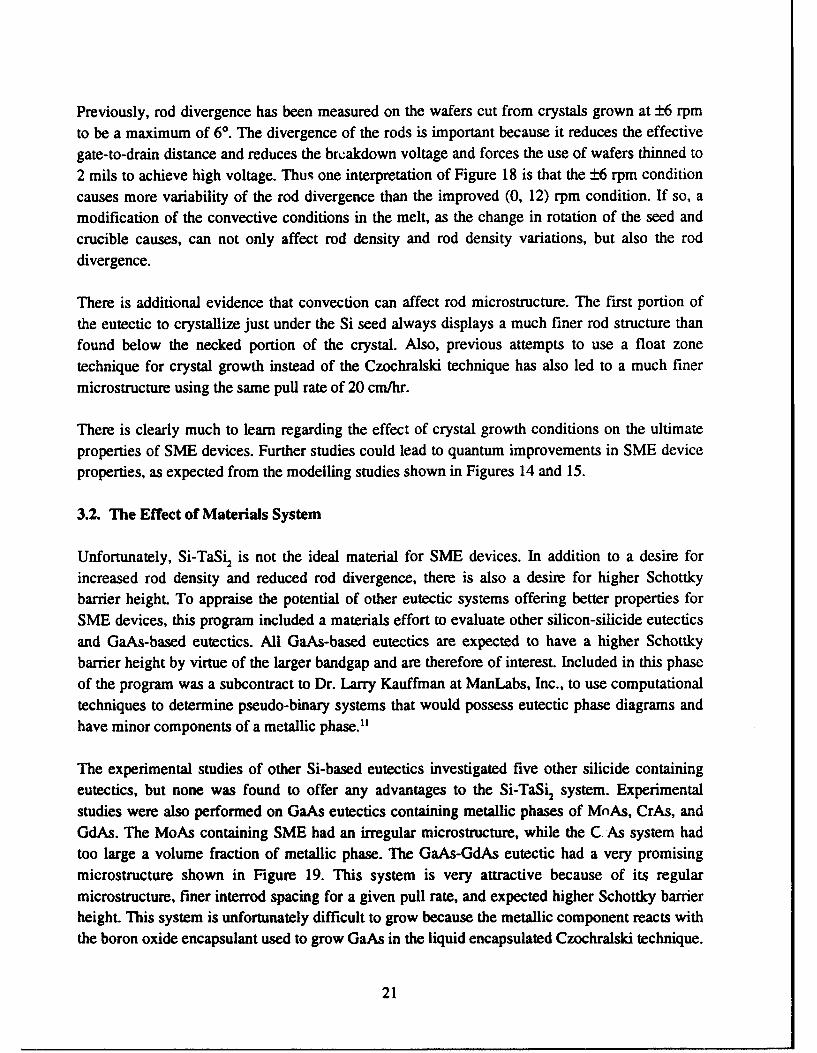
Previously, rod divergence has been measured on the wafers cut from crystals grown at ±6 rpmto be a maximum of 6*. The divergence of the rods is important because it reduces the effectivegate-to-drain distance and reduces the bwakdown voltage and forces the use of wafers thinned to2 mils to achieve high voltage. Thus one interpretation of Figure 18 is that the ±6 rpm conditioncauses more variability of the rod divergence than the improved (0, 12) rpm condition. If so, amodification of the convective conditions in the melt, as the change in rotation of the seed andcrucible causes, can not only affect rod density and rod density variations, but also the roddivergence.
There is additional evidence that convection can affect rod microstructure. The first portion ofthe eutectic to crystallize just under the Si seed always displays a much finer rod structure thanfound below the necked portion of the crystal. Also, previous attempts to use a float zonetechnique for crystal growth instead of the Czochralski technique has also led to a much finermicrostructure using the same pull rate of 20 cm/hr.
There is clearly much to learn regarding the effect of crystal growth conditions on the ultimateproperties of SME devices. Further studies could lead to quantum improvements in SME deviceproperties, as expected from the modelling studies shown in Figures 14 and 15.
3.2. The Effect of Materials System
Unfortunately, Si-TaSi2 is not the ideal material for SME devices. In addition to a desire forincreased rod density and reduced rod divergence, there is also a desire for higher Schottkybarrier height. To appraise the potential of other eutectic systems offering better properties forSME devices, this program included a materials effort to evaluate other silicon-silicide eutecticsand GaAs-based eutectics. All GaAs-based eutectics are expected to have a higher Schottkybarrier height by virtue of the larger bandgap and are therefore of interest. Included in this phaseof the program was a subcontract to Dr. Larry Kauffman at ManLabs, Inc., to use computationaltechniques to determine pseudo-binary systems that would possess eutectic phase diagrams andhave minor components of a metallic phase."
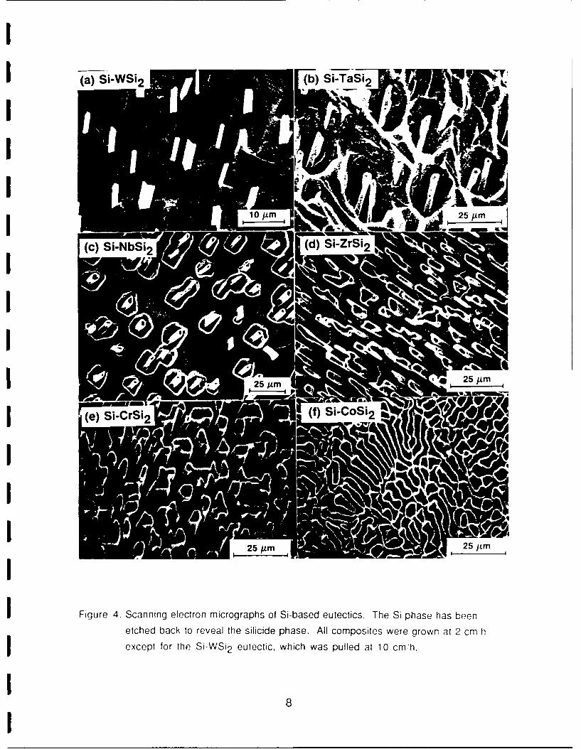
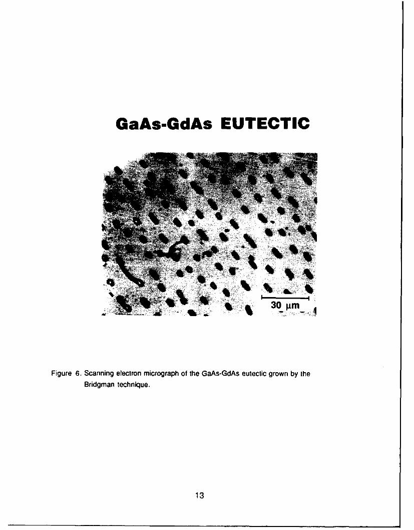
The experimental studies of other Si-based eutectics investigated five other silicide containingeutectics, but none was found to offer any advantages to the Si-TaSi 2 system. Experimentalstudies were also performed on GaAs eutectics containing metallic phases of MnAs, CrAs, andGdAs. The MoAs containing SME had an irregular microstructure, while the C. As system hadtoo large a volume fraction of metallic phase. The GaAs-GdAs eutectic had a very promisingmicrostructure shown in Figure 19. This system is very attractive because of its regularmicrostructure, finer interrod spacing for a given pull rate, and expected higher Schottky barrierheight. This system is unfortunately difficult to grow because the metallic component reacts withthe boron oxide encapsulant used to grow GaAs in the liquid encapsulated Czochralski technique.
21

Kauffman has also indicated that borides should form eutectics with GaAs, and these systemsshould also be examined. Further efforts on the crystal growth of these systems and the GdAscontaining system could prove very fruitful.
P4 4 4L
1%6 30 gm
Figure 19.Scanning electron micrograph of the GaAs-GdAs eutectic grown by the Bridgmantechnique.
One other technique has been investigated during this program to develop a higher barrier heightmaterial. This is to convert the Schottky junctions in the Si-TaSi2 to p/n junctions. This would bebeneficial because the leakage from the Schottky junctions would be significantly reduced, andthe carrier concentration, and therefore the current switching capability, would also likey beincreased. Substantial progress toward this goal has been achieved in this program. It has beenshown that the TaSi2 rods can be completely removed from a 10 mil thick wafer. With wafershaving the metallic component removed, diffusion studies with a Boron source have beenconducted. However, a test to determine the success of this diffusion step is difficult to developand has delayed completion of this task. Nevertheless, this is a very promising approach and, ifproperly pursued, will likely lead to significantly improved devices.
22

I
1 4. IMPLICATIONS FOR PULSED POWER APPLICATIONS AND SUMMARY
j During the course of this program, many scientific and engineering milestones have beencompleted.
I From a materials science perspective, it has been shown for the first time that a two-phaseequilibrium structure can perform as the basis for electronic devices. Prior to this, only single-
j phase or metastable structures such as superlattices have been considered suitable for electronicdevices. The accomplishments of this program will hopefully set the precedent for a wide rangeof new materials for electronic applications.
In device physics, it has been shown for the first time that floating junctions can extend thebreakdown voltage of depletion mode devices beyond the avalanche breakdown limit. This is amajor innovation in semiconductor device physics that will hopefully lead to a new generation ofhigh-voltage, high-current devices.
In pulsed power, it has been shown that semiconductor-metal eutectic devices offer the threeingredients of high voltage, high current, and rapid opening times. Although the current state-of-the-art in SME does not excel in each of the three categories relative to conventional devices,they clearly have a place in the competetive, well-developed field of high-power devices. This isparticularly impressive in the light of the small program.
Nevertheless, commercialization of SME devices and realization of their full potential will takeadditional development. The following research and development program is recommended tocomplete the development of these novel devices.
1. A high-voltage, high-current SME prototype device should be demonstrated and testedusing methods already employed to evaluate conventional devices such as the SIT or
the MOS-controlled thyristor. Initially, we proposed a 100 A, 10 kV test. A similargoal should be pursued and tied to a specific application. The program should includegrowth of large diameter crystal, fabrication of large area devices, packaging ofdevices, and testing of devices. The actual opening time for the switch should bemeasured. It could be significantly less than the upper limit of 15 ns demonstrated in
this program.
2. A next-generation material should also be developed for a substantial leap in thecurrent handling capability of an SME device. An enhanced material that wouldexceed the switching capability of MOS-controlled thyristors and other advancedconventional devices in all three categories of high voltage, high current, and switching
time would need to have a higher barrier height, a finer interrod spacing, and an
23

increased carrier concentration in the semiconductr matrix. Three possibilities forachieving this have already been discussed: 1) a growth technique that leads to finerinterrod spacing in the Si-TaSi2 system, 2) GaAs based eutectics, and 3) Si-TaSi2 withthe Schottky junctions converted to p-n junctions. A long-term research programdedicated to achieving an order of magnitude improvement in the capabilites of solid-state switches should include a program that pursues all three approaches. All threehave a good probability for success.
In summary, SME devices have great potential for pulsed power switching as well as otherapplications, and the technology is very close to being ready for commercialization. Therefore, itis unfortunate that due to extraneous circumstances, GTE has discontinued its research anddevelopment program in this area. It is our recommendation that some method of seeing thework through to a successful conclusion be sought and implemented.
24

5. REFERENCES
1. B.M. Ditchek, T.R. Middleton, P.G. Rossoni, and B.G. Yacobi, Appl. Phys. Lett. 52, 1147(1988).
1 2. Q.V. Nguyen, P.G. Rossoni, M. Levinson, and B.M. Ditchek, Proceedings of 20thInternational Symposium on Power Modulator, Myrtle Beach, SC (1992).
3. S.M. Sze, Physics of Semiconductor Devices, Wiley, New York (1969).
1 4. M. Levinson, P.G. Rossoni, W.W. Byszewski, and B.M. Ditchek, Proceedings of 19thPower Modulator Symposium, San Diego, CA (1990).
5. M. Levinson, P.G. Rossoni, F. Rock, and B.M. Ditchek, Electron. Lett. 26, 777 (1990).
1 6. M. Levinson, Q.V. Nguyen, P.G. Rossoni, and B.M. Ditchek, ONR Review, CA (1991).
j 7. P.G. Rossoni, M. Levinson, and B.M. Ditchek, J. Appl. Phys. 70, 2861 (1991).
8. B.J. Baliga, IEEE Spectrum, p. 42 (March 1981).
9. C. Braun, Proceedings of the 4th SDIO/ONR Pulse Power Meeting, p. 88 (1991).
I 10. Q.V. Nguyen, T.R. Middleton, J. Hefter, and B.M. Ditchek, AACG Crystal Growth
Conference, Fallen Leaf Lake, CA (1991).
11. L. Kauffman and B.M. Ditchek, J. Less Common Metals 168, 115 (1991).
25

IIIII
II
II
III
IResearch &
Development
IIII
Semiconductor-Metal EutecticComposites for High PowerSwitching
Final Report for Contract N0014-86-C-0595
B.M. DitchekM. Levinson
Submitted toDr. Gabriel RoyOffice of Naval Research
1 800 North Quincy StreetArlington, VA 22217-5000
April 1990
I GTE Laboratories incorporated40 Sylvan RoadWaltham, MA 02254

I
TABLE OF CONTENTS
1. Introduction 1
2. Eutectic Composite Materials 2
2.1 Si-Based Eutectic Systems 2
2.2 GaAs-Based Eutectics 7
3. Eutectic Composite Materials 17
3.1 Diode Contacts 17
3.2 Diode Characterization 18
4. Transport in Eutectic Composite Materials 21
5. Eutectic Composite Transistors 26
5.1 Transistor Design and Characterization 26
5.2 Transistor Characteristics 26
5.3 EBIC Characterization 33
5.4 Modeling of Transistor Characteristics 36
5.5 Pulsed Tests 43
6. Implications of Pulsed Power 45
7. References 47
Appendix: Publications on Contract
Related Publications

LIST OF FIGURES
Figur PAI
1 Photograph of a typical single-crystal (111) matrix Si-TaSi2 eutectic composite. 4
2. A transverse section of a Si-TaSi2 eutectic composite. Note the cellular
arrangement of the TaSi2 rods. 4
3. A color coded contour plot of the rod density of a quarter section of a wafer. The
analysis area for each pixel in this case is 5000 jim 2 . The numbers on the right
refer to the number of rods counted in a pixel of a given color. The figure
demonstrates the swirl-like distribution of rods in a wafer. 6
4. Scanning electron micrographs of Si-based eutectics. The Si phase has been
etched back to reveal the silicide phase. *All composites were grown at 2 cm/h
except for the Si-WSi 2 eutectic, which was pulled at 10 cm/h. 8
5. Scanning electron micrographs of two GaAs-based eutectics. The microstructure
of the GaAs-MoAs eutectic is shown in (a) and the microstructure of the GaAs-CrAs
eutectic is shown in (b). Both were pulled at 6 cm/h. 10
6. Scanning electron micrograph of the GaAs-GdAs eutectic grown by the
Bridgman technique. 13
7. Optical micrographs of (a) axial and (b) transverse sections of the GaAs-CrAs
eutectic grown in a magnetic field (2.5 kG). The axial slice shows periodic
rotational bands, with a spacing of 100 lim. The transverse slice, intersecting
these bands, shows a spiral pattern. (b) shows a micrograph of one section of
this spiral indicating that the contrast is due to a change in interrod spacing.
For (b) the magnification is 185 x. 15
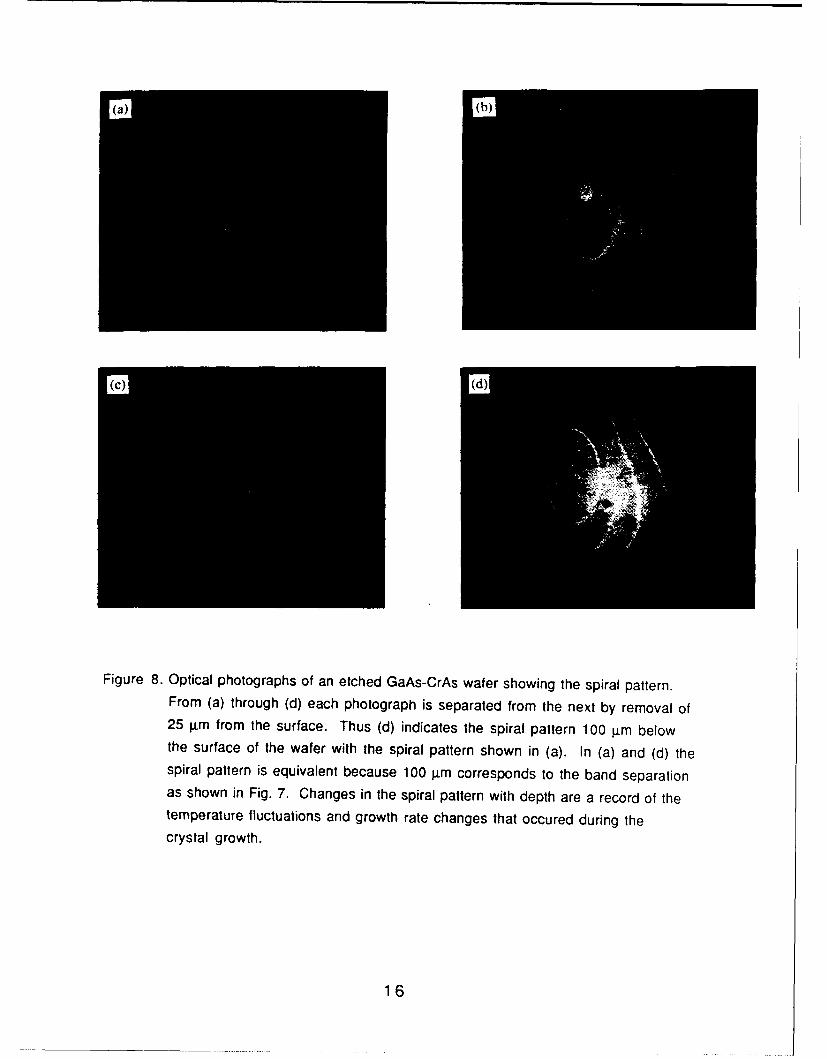
8. Optical photographs of an etched GaAs-CrAs wafer showing the spiral pattern.
From (a) through (d) each photograph is separated from the next by removal of
25 jim from the surface. Thus (d) indicates the spiral pattern 100 jim below
the surface of the wafer with the spiral pattern shown in (a). In (a) and (d) the
Hi

spiral pattern is equivalent because 100 I1m corresponds to the band separation
as shown in Fig. 7. Changes in the spiral pattern with depth are a record of the
temperature fluctuations and growth rate changes that occured during the
crystal growth. 16
9. Schematic showing method used to form self-aligned CoSi 2 gate contacts. 1 9
1 0 .Scanning electron micrographs showing EBIC images of the depletion zones
around rods without a bias voltage (b) and with a 5 V reverse bias (c). 2 0
11 .Correlation of the EBIC and Hall carrier concentration ratio (nEBIC/nH)as a function of the matrix carrier concentration. The significant increase
in this ratio below 2 x 1015 cm- 3 is due to depletion zone limited transport. 25
1 2.A quarter section of the concentric ring pattern of source, drain and gatecontacts used to fabricate the transistor. 27
1 3.Schematic procedure for fabricating ohmic contacts that are insulated fromthe metallic rods of a eutectic composite. 28
1 4.The transfer characteristics of a Si-TaSi2 eutectic composite transistor that
blocks 1000 V. 31
15 .A schematic model showing how the effective gate to drain distance changesas a function of wafer thickness due to rod divergence. 32
1 6.The circuit diagram used for the three terminal EBIC technique. 34
1 7.Three terminal EBIC micrographs of a eutectic composite transistor with (a)no gate bias and (b) a 10 V reverse bias. Both transistors have a source to
drain voltage of 90 V. The dark channels emanating from the gate ring indicate
regions of current saturation. 35
1 8.Model simulation geometries: gate rod only (left): with floating rods(right). 3 8
1 9. Potential vs. distance from the source: (1) gate rod only; (2) with floating rods. 3 9
,III

20.Maximum electric field vs. drain voltage: (1) gate rod only; (2) with floating
rods. 40
21 .Model predictions of the electric field as a function of distance from the drain
for the case of no gate bias and (a) 100 Vsd, (b) 200 Vsd, and (c) 400 Vsd.At low drain voltages Emax saturates. Once the depletion zone reaches the drain,
an increase in the drain voltage causes the field at the last rod to exceed the
saturation Emax and eventually cause breakdown. 41
22 .Schematic diagram of the high voltage plasma discharge apparatus. 44
iv

LIST OF TABLES
I. Microstructural parameters for Si-silicide eutectics. 9
II. Eutectic phase diagrams calculated using CALPHAD techniques. 1 2
II. Depletion zone limited transport. 25
IV. Factors affecting the maximum blocking voltage. 31
V. Model calculations of SME transistor parameters for combinationsof carrier concentration and interrod spacing that will yield a
maximum electric field of 100 kV/cm. 42
V

1. INTRODUCTION
Semiconductor-metal eutectic (SME) composites, with a microstructure composed of an
array of metallic rods distributed throughout a semiconductor matrix and formed by the
directional solidification of a eutectic mixture, represent a new class of electronic materials
with the potential to enhance and expand the capabilities of high-power, solid-state
switching technology of most interest to the pulsed power community as well as other areas
including photodetection. The objective of this three-year program has been to establish the
materials science and device principles necessary to assess the feasibility of high power
switching devices based on SME materials.
In this report, the most important results of the SME studies over the course of this contract
will be reviewed. Important contributions have been made in the growth of these materials,
including growth factors that affect the rod structure and in the identification of new GaAs-
based SME systems. The development of high power transistors in the Si-TaSi2 'benchmark'
system will be discussed and it will be shown that the rapid progress that has led to 1 kV
blocking voltage devices can probably be continued to yield true high current, high voltage
opening switches. The goals of materials development and bringing the device development to
the point of assessing pulsed power capabilites have been met.
This program has followed a radical approach to the development of advanced electronic
materials and, in particular, high power opening switches. SME materials differ from the
single-phase materials that have been used to create electronic devices in the past in that
they contain two phases in equilibrium with each other. Long held tenets of semiconductor
device physics required that the semiconductor be made free of any second phase. It was
believed that metallic inclusions would lead to high leakage currents and low-voltage
breakdown. The development and demonstration of SME composite materials for high-voltage
operation in this program has given credibililty to this radical approach and has reduced the
credibility of the old semiconductor tenets thereby opening up device design to freer thought,
and, hopefully, more innovation.

2. EUTECTIC COMPOSITE MATERIALS
2.1 Si-Based Eutectic Systems
The directional solidification of the Si-TaSi 2 eutectic composite yields a material with a
rod-like distribution of the TaSi2 phase in a Si matrix. The eutectic composition
corresponds to about 2 v/o TaSi2 . The scale of the eutectic microstructure is determined by
the growth rate, such that X2 v is a constant, where X. is the average interrod spacing and v is
the growth rate. The constant has been determined in these studies to be 1.25 x 10- 5
cm 3 /h. All devices have been fabricated in material grown at 20 cm/h and contained an
average interrod spacing of about 8 g±m.
The growth technique employed is called Czochralski crystal pulling and is analogous to the
most common technique for growing large Si crystals for the electronics industry. After the
melting of a charge of the eutectic composition a Si seed is lowered onto the melt surface,
given time to thermally equilibrate, and then pulled up at the fixed rate of 20 cm/h. The
composite boule solidifies as the seed is pulled. This process of directional solidification
yields the eutectic rod-like microstructure with the rods oriented along the growth
direction.
Initially, the boules grown had polycrystalline Si matrices. Fabrication of devices on these
substrates always led to excessive leakage and nearly ohmic, nonrectifying behavior. It was
found, however, that composites with a single-crystal Si matrix could be obtained using
certain techniques. Growth of a single-crystal matrix eutectic depends primarily on using
the exact eutectic composition and minimizing certain impurities. Due to loss of Si as SiO and
the meltback of a fraction of the seed, maintaining the eutectic composition can be difficult.
Nevertheless, proper balancing of the two effects can be achieved and numerous boules with
single crystal matrices have been grown. Originally, all boules were grown with a (111)
single crystal matrix of Si and all devices were fabricated in (111) material. Studies of the
effect of orientation on microstructure were conducted, however, leading to composite boules
with (110) and (100) orientations as well. The results of this study are discussed later.)
For this program, Si-TaSi 2 boules were typically grown with a diameter of about 2 cm and
2

weighed between 50 and 100 gms. A photograph of a typical single-crystal matrix (111)
boule is shown in Fig. 1. The eutectic microstructure in a typical transverse section is
shown in Fig. 2. The figure shows that the rods in the eutectic are neither arranged in a
regular lattice-like array nor distributed in a strictly random pattern. Examinations of
many such sections has revealed a kind of cellular structure. The interrod spacing in the cell
walls is less than the average interrod spacing. For the case of X = 8 p.m, our estimates
indicate that the spacing within the cell walls averages only about 4.5 p.m. The interior of
the cell walls exhibits a very low rod density and covers an area with a diameter several
times the average interrod spacing. Studies of the transport properties of the composites
have indicated that the cellular nature of the rod distribution tends to limit the conductivity
at a much higher carrier concentration than it would for a regular 8 p.m interrod spacing
distribution and, therefore, the irregularity of the structure, contrary to intuition, offers
advantages to the device performance.
Examination of longitudinal sections of the boule also indicates that the rods are not all
perfectly aligned and that some divergence of the rods relative to the wafer normal may exist.
Using the EBIC technique discussed in Section 3, the maximum divergence of the rods has
been measured to be 6 0 relative to the wafer normal. Rod misalignment has been shown to be
a microstructural factor adversely affecting switch performance (Section 5.3).
Since the TaSi2 /Si Schottky barrier is higher on n-type Si than on p-type, the Si used in the
charge was always lightly doped with the n-type dopant, phosphorous. Carrier
concentrations of the composite boules, 1 to 3 x 1015 cm- 3 , were several times larger than
the carrier concentrations of the Si charge, indicating that the Ta was probably contaminated
with an n-type doping element, such as P. Segregation of the dopant along the axis of the
boule indicated complete mixing in the melt and a segregation coefficient that was similar to
that for n-type dopants in Si, about 0.3.
Studies of the Si composite boules took two approaches. First, to develop an understanding of
the growth factors affecting microstructure, particularly, the rod density, rod misalignment
and the matrix orientation. Second, to determine if any other Si-based eutectics offered a
microstructure more favorable to device development.
3

01 Laboratories0 1 2 3
ich
cm KY--KY
Figure 1. Photograph of a typical single-crystal (111) matrix Si-TaSi 2 eutectic
composite.
10Um
Figure 2. A transverse section of a Si-TaSi2 eutectic composite. Note the cellular
arrangement of the TaSi 2 rods.
4

II
The classic theory of eutectic solidification implies little or no affect of melt convection on
the interrod spacing. Laminar flow leads to a boundary layer that is much larger than the
interrod spacing, which according to the theory of eutectic solidification is comparable in
extent to the maximum compositional variations in the melt extending outward from the
melt-solid interface. Nevertheless, these materials are grown under the turbulent melt
conditions of Czochralski growth, and temperature fluctuations and growth rate variations
are expected. Analysis of these effects proceeded using an image analysis technique
performed in a JEOL JXA-84011 scanning electron microscope (SEM). Data image
acquisition and processing was done using a Tracor Northern 5500 system. The system was
used primarily to count the number of rods in a given area, typically 90 g±m x 90 p.m. Using
this technique diameter scans and areal scans were made to correlate average rod density and
rod density variations across a wafer with growth parameters.
The microstructural analysis indicated two effects important for understanding and designing
I devices with this material. Firstly, the wafers contain a variation in rod density that maps
out a spiral. It originates near the wafer center and spirals to the wafers edge. A quarter
section of a wafer that has been analyzed is shown in Fig. 3. The number of rods within a 80
,.-n2 area vary from a high of 100 to a low of 60, all within the same wafer. Indications are
that these variations depend on the rotation rate of both the seed and crucible. Secondly, the
actual rod density averaged over the entire wafer, decreases slightly as the orientation of the
1 Si matrix goes from (111) to (100) or (110) and as the rotation rates of the seed and
crucible are increased. In addition, rapid rotation rates, about 30 rpm, was noted to yield
large excursions in composition, such that parts of the wafer contained single phase Si
regions without the TaSi 2 rods.
I Studies of GaAs-based eutectics, to be discussed in detail in the following section, indicate
that the spiral distribution of interrod spacings changes along the boule axis. Thus, the rod
density at one point, (x,y,O) at the surface of a wafer is different from the rod density at
another point a distance I below the surface point (x,y,/. Divergence or misalignment of
the rods is required to explain this. This implies that the divergence of the rods which
reduces the blocking voltage of a device and places restrictions on the maximum usable
I thickness of a wafer and, therefore, the current handling ability of the device, is partly
caused by the effect that leads to the spiral pattern.
5

o F
00
0
in, a,C,, *u
Co 0 Ca0
S 0)ox0 C a,0
me -6
0 0 Z =,
In0 0~L
0~ ~~~ m 0
6CIa

II
The swirl pattern is almost certainly caused by the temperature fluctuations during growth
in a Czochralski crystal growth system. The temperature fluctuations yield growth rate
variations and this, through the X2 v = a contant rule, causes a variation in the interrod
spacing. Improved uniformity would probably be expected in Bridgman growth but this
technique cannot be applied to growth of the high temperature Si-based systems. It is known
that a magnetic field can be used to minimize temperature fluctuations but even the thermal
nonuniformities in the system can lead to growth rate variations due to seed rotation.
Improved uniformity may come from maximization of thermal symmetry in the growth
system and optimized rotation rates.
Many other Si-silicide eutectics exist in addition to the Si-TaSi2 system. The systems listed
in Table I were grown and their microstructure characterized. Micrographs for each
system, showing the variations in the volume fraction of the silicide phase are shown in Fig.
4. Table I lists the X2 v constant, and the rod diameter, d, for each system at a growth rate of
10 cm/h. An examination of the values of X2 v for each system shows that the constant
decreases as the volume fraction of the silicide phase increases, such that, the d2 v value is
nearly constant for all the Si-silicide systems. This leads to a similarity of these systems
that does not point to an advantage of one eutectic system over the Si-TaSi 2.
2.2 GaAs-Based Eutectics
The purpose of studying GaAs-based eutectics was to identify and develop new eutectic
composites with enhanced properties. The most desirable property expected was that of a
higher Schottky barrier height. Barrier heights in this system are expected to be at least
0.7 eV, or better than half the bandgap of GaA . Thus, these systems should enable high
power devices with reduced leakage currents and more temperature stability.
5GaAs-based eutectics were essentially virgin territory. Only one reference was known to us:
a paper by Reiss and Renner1 on three GaAs rod-Ike eutectics, GaAs-CrAs, -MoAs and VAs.
5The approach we took was to re-examine these three systems and use phase diagram
calculations followed by experimental work to evaluate others. Microstructure of the GaAs-
ICrAs and the GaAs-MoAs are shown in Fig. 5. Both systems were grown by the high pressure,liquid encapsulated Czochralski (LEC) technique. Encapsulation and the growth and synthesisI
I
I
I (a(b) Si-TaSi ,
III
S10//Am 25 E m
(c) Si-NbSi2
III
I (e) S3-CrSi 2i2
II
25/J~m2514.m
Figure 4. Scanning electron micrographs of Si-based eutectics. The Si phase has been
etched back to reveal the silicide phase. All composites were grown at 2 cm h
except for the Si-WSi2 eutectic, which was pulled at 10 cm'h.
8

E
-n a LO ta L *
(5 cm 0Ir m V
*ot C4 o 0) o) OI i CI a- C.m LOC
co

ItI
a0
Cc
E 0
Cc-
10 0

under high pressure are techniques needed to suppress loss of the volatile As component. The
GaAs-CrAs system is a rod-like eutectic with a volume fraction of metallic phase that is too
large for device applications. Device applications are also precluded by the interconnectivity
of the CrAs rods. The GaAs-MoAs system tends to yield a very irregular distribution of the
MoAs phase. The As-Mo phase diagram has several different arsenides in it and these
probably also appear in the composite as As is lost. The GaAs-VAs system was not
investigated because a V source of reasonable purity was not available.
Phase diagram calculations intended to help identify additional GaAs-based eutectics were
conducted by Dr. Larry Kaufman of ManLabs Inc. using CALPHAD techniques. This work was
performed under subcontract to the main program. The systems listed in Table II have been
identified as having eutectic compositions using this technique. Calculated eutectic
compositions and temperatures are listed for each system. The GaAs-CrAs and GaAs-MoAs
systems, with known eutectic compositions, were used as controls and the computed values
compared very favorably with experimental values from our work and that of Reiss and
Renner.
Of the other systems present only the GaAs-GdAs system was grown. This system and others
containing rare earth arsenides are difficult to grow using the LEC technique because the rare
earth reacts with the encapsulant forming a rare earth oxide that is.impenetratable by the
seed. Using Bridgman techniques the GaAs-GdAs system was grown. The microstructure of a
cross-section is shown in Fig. 6. The system does have a volume fraction of the metallic
phase that is appropriate for device development. Use of this system will require
development of better techniques for growing it that will provide better composition control
than the currently used Bridgman technique offers and enables routine growth with a single
crystal matrix. Experiments have been performed substituting BaCI2 for B2 0 3 encapsulant.
But even though the chloride doesn't react with rare earths, it does melt at a higher
temperature and it is not as simple to work with as the oxide. Nevertheless, this system is
very promising and with sufficient effort it should be possible to fabricate device quality
material. As shown in Fig. 6, the GaAs-GdAs also offers the advantage of a slightly reduced
interrod spacing relative to the Si-TaSi 2 system.
Growth studies of the GaAs-borides have not been carried out to the point of verifying the
11

ci
CD LO 0 0 ~- 0~ 0IT LO) V) V) Wrt LI)
w
0
X0oj N 00 0 -0 0
0 C;C ; ;0C
-5.-
UL
a1 cl) ) cn C 4 N
<< < <a cc D00
-C-E z o -4
w
12
GaAs-GdAs EUTECTIC
Figure 6. Scanning electron micrograph of the GaAs-GdAs eutectic grown by theBridgman technique.
13

ManLabs prediction of a eutectic in this system. If these predictions are correct, it should
offer a low volume fraction rod-like structure. Presumably the boron, which is
isoelectronic with Ga, will not affect the conductivity of the GaAs lattice.
The GaAs-CrAs system, simple to grow and with a microstructure that is easy to analyze, has
been used for studies of the effect of convection on the rod structure. Reference has been
made to these studies in the previous section on Si-based systems. Composites were grown in
a system with a transverse magnetic field. The magnet is used in crystal growth studies to
suppress turbulent convection and reduce temperature fluctuations in Czochralski growth.
Composite boules grown in a magnetic field were sliced into wafers and etched. The etched
wafers reveal a sharp spiral pattern which from a micrograph of the spiral line, clearly
represents a region in the wafer with a large interrod spacing and rod diameter. Thus, the
spiral pattern, except for the additional sharpness caused by the application of the magnetic
field, is similar to that observed in the Si-TaSi2 system. Micrographs are shown in Fig. 7.
In Fig. 7(a) a longitudinal cut shows the rods along their axis and the periodic change that
results. The transverse wafer contains the spiral and Fig. 7(b) shows a micrograph of this
area indicating the change in rod density observed along the spiral line. In this case, the
interrod spacing variations are sufficiently large as to be readily observed without image
analysis techniques.
The etched wafer is shown in Fig. 8 in a sequence that shows how the spiral changes along the
boule axis. The micrograph in part (a) was taken, the wafer was polished and re-etched
after removal of 25 gim, or one quarter of the banding period apparent from Fig. 7(a). This
micrograph from this position is shown in Fig. 8(b). The distribution of the spiral is
slightly different in (b) vs (a). This was continued until 100 gm was removed. After 100
p.m removal, the length of the banding period, the original spiral distribution is re-
established. This technique allows construction of a three dimensional distribution of the rod
density variations and clearly leads to the conclusion that divergence of the rods is required
to accomodate the density changes along the axial direction.
14

(a) (b)
Figure 7. Optical micrographs of (a) axial and (b) transverse sections of the GaAS-CrAseutectic grown in a magnetic field (2.5 kG). The axial slice shows periodicrotational bands, with a spacing of 100 gim. The transverse slice, intersectingthese bands, shows a spiral pattern. (b) shows a micrograph of one section ofthis spiral indicating that the contrast is due to a change in interrod spacing.For (b) the magnification is 185 x.
15
(a) (b)
(c) (d)
Figure 8. Optical photographs of an etched GaAs-CrAs wafer showing the spiral pattern.From (a) through (d) each photograph is separated from the next by removal of25 lam from the surface. Thus (d) indicates the spiral pattern 100 p.m belowthe surface of the wafer with the spiral pattern shown in (a). In (a) and (d) thespiral pattern is equivalent because 100 .m corresponds to the band separationas shown in Fig. 7. Changes in the spiral pattern with depth are a record of thetemperature fluctuations and growth rate changes that occured during thecrystal growth.
16
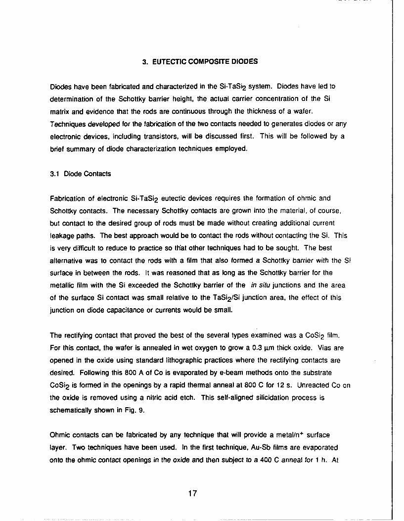
3. EUTECTIC COMPOSITE DIODES
Diodes have been fabricated and characterized in the Si-TaSi 2 system. Diodes have led to
determination of the Schottky barrier height, the actual carrier concentration of the Si
matrix and evidence that the rods are continuous through the thickness of a wafer.
Techniques developed for the fabrication of the two contacts needed to generates diodes or any
electronic devices, including transistors, will be discussed first. This will be followed by a
brief summary of diode characterization techniques employed.
3.1 Diode Contacts
Fabrication of electronic Si-TaSi 2 eutectic devices requires the formation of ohmic and
Schottky contacts. The necessary Schottky contacts are grown into the material, of course,
but contact to the desired group of rods must be made without creating additional current
leakage paths. The best approach would be to contact the rods without contacting the Si. This
is very difficult to reduce to practice so that other techniques had to be sought. The best
alternative was to contact the rods with a film that also formed a Schottky barrier with the Si
surface in between the rods. It was reasoned that as long as the Schottky barrier for the
metallic film with the Si exceeded the Schottky barrier of the in situ junctions and the area
of the surface Si contact was small relative to the TaSi2 /Si junction area, the effect of this
junction on diode capacitance or currents would be small.
The rectifying contact that proved the best of the several types examined was a CoSi 2 film.
For this contact, the wafer is annealed in wet oxygen to grow a 0.3 gim thick oxide. Vias are
opened in the oxide using standard lithographic practices where the rectifying contacts are
desired. Following this 800 A of Co is evaporated by e-beam methods onto the substrate
CoSi2 is formed in the openings by a rapid thermal anneal at 800 C for 12 s. Unreacted Co on
the oxide is removed using a nitric acid etch. This self-aligned silicidation process is
schematically shown in Fig. 9.
Ohmic contacts can be fabricated by any technique that will provide a metal/n + surface
layer. Two techniques have been used. In the first technique, Au-Sb films are evaporated
onto the ohmic contact openings in the oxide and then subject to a 400 C anneal for 1 h. At
17

this temperature, above the Au-Si eutectic, the Au reacts with the substrate and the ohmic
contact is formed via the Sb-doped n+ layer at the junction. Since the eutectic film is
irregular and discontinuous in most cases, it is necessary to evaporate an additional metallic
layer, usually, another Au film on top of the reacted film. The second approach yields a more
robust, uniform contact. In this technique a CoSi2 film is formed as it was for the Schottky
contact. To form the n+ contact at the silicide/Si junction, As is implanted at 100 kV with a
flux of 1014 cm- 2 . Movement of the As from the surface of the silicide film to the junction
was performed with another rapid thermal anneal at 800 C to 900 C for 10 s. In exacting
applications, this ohmic contact was preferred.
3.2 Diode Characteriztion
Diodes have been characterized using a variety of techniques including, current-voltage (I-
V), capacitance-voltage (C-V), deep level transient spectroscopy (DLTS) and electron-
beam-induced-current techniques (EBIC). A number of important conclusions resulted from
these studies that are relevant to device development for high power applications. Some of
these are discussed briefly in the following.
. The I-V characteristics of the diodes were nearly ideal. The forward characteristics
indicated an ideality factor of 1.1 and reverse bias resulted in leakage currents that were
nearly constant below 10 V and comparable to the expected value based on the Schottky
barrier height. The Schottky barrier height was determined to be 0.62 eV.
• The C-V characteristics indicated that the junctions acted as coaxial capacitors rather than
parallel plate capacitors as expected from the rod-like shape of the junctions. At high
reverse bias voltages, the capacitance was lower than expected probably because of overlap of
the depletion zones of neighboring junctions.
* DLTS indicated good quality Si surrounded the junctions. The concentration of electrically
active Ta-induced levels was found to be inconsequentially small. Other traps, probably
related to dislocation-induced levels were found to be inhomogenously distributed.
* EBIC techniques gave the first graphic images of the depletion zones surrounding the rods.
It showed that expansion or contraction of the depletion zone could be affected by a reverse or
forward bias, repectively. Furthermore, by relating the actual rate of increase of the
depletion zone with reverse bias voltage to that expected for a cylindrical junction based on
Poisson's equation, EBIC was used as a method for accurately determining the carrier
18

concentration of the Si matrix. SEM and EBIC micrographs of several TaSi2 rods in a Si
matrix at zero bias and with a 5 V reverse bias voltage are shown in Fig. 10.
Step 1. Oxidize, open gate window and deposit Co
.o01' 77 1? -- Co7-" OXIDE
ICOMPOSITE
TaSi 2
I Step 2. Anneal (8000 C - 12s) to form CoSi 2, remove
i excess Co and make ohmic contact
CoSi 2 OHMIC~CONTACT
I [OMPOSITE
TaSi 2
Figure 9. Schematic showing method used to form self-aligned CoSi2 gate contacts.
19
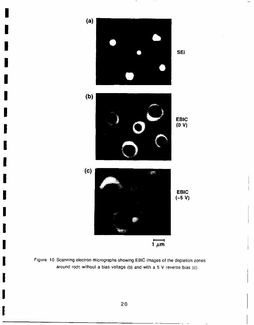
I(a)
SEIII
m (b)
EBI(o V)
(c)
EBIC(-5 V)
I
I Figure 10. Scanning electron micrographs showing EBIC images of the depletion zonesaround rods without a bias voltage (b) and with a 5 V reverse bias (c).I I2

I4. Transport in Eutectic Composite MaterialsI
In the design of high power opening switches or transistors, the series resistance and
transconductance of the device, both of which depend on the basics of transport in the device
material, must be optimized. Thus, understanding the physics of electron transport in
eutectic composites, is clearly important for device design.
At the beginning of the program, it was clear that the transport of electrons in this composite
material would be affected by the presence of the in situ depletion zones. If depletion zones
are small and do not consume a volume fraction significantly larger than the volume fraction
Iof the second phase, TaSi2 , about 2 %, then the composite resistivity should be that of the Si
matrix. In the other extreme, if depletion zones are sufficiently large to cause intersection
Iof depletion zones around neighboring rods, then the material should be in the 'pinched-off'
state and have a resistivity that is much higher than the Si matrix resistivity given by its
carrier concentration and mobility.
The effect of the depletion zones on transport in regions between these extremes was
determined from an analysis of the Hall effect and EBIC techniques. As discussed in the
previous section, EBIC provides a technique for accurately measuring the carrier
concentration in the Si matrix. For a given rod diameter, since the depletion zone size is a
function of the carrier concentration and the applied bias voltage only, fitting the EBIC
measured depletion zone size to its functional dependence on reverse bias voltage provides a
sensitive measure of the local carrier concentration of the Si matrix.
With the Si matrix carrier concentration and the Hall effect carrier concentration, the effect
Iof depletion zone volume on the composite transport properties was analyzed based on a model
by Read. 2 Read analyzed the composite resistivity and Hall effect of a semiconductor with an
Iarray of parallel space-charge cylinders in a semiconductor. The model, developed long
before directionally solidified eutectics were of interest, was originally applied to dislocation
arrarys. Read considered that the in situ space charge cylinders could affect transport by
scattering directly from space charge cylinders, reduction in the average concentration of
jcharge carriers, and distortion of the current streamlines.
21

IConsidering the large interrod spacings relative to the room-temperature electron-mean-
free path, the first effect is negligible. Hence, the actual mobility of the electrons in the
semiconductor matrix will not be affected by the in situ depletion zones. The second effect is
simple to consider; due to the volume of material in the depletion zones the carrier
concentration averaged over the entire composite volume will be less than the localized
carrier concentration of material between the depleted zones. In a composite with rods of
radius ro and a rod density Nr, the volume fraction of the depleted material, E, is
I = n (ro + W)2 Nr, (1)
i where W is the depletion zone width. The average concentration is given by
I <n> = n(1-F). (2)
The final effect of current streamlining was included through a definition of the current
streamlining function, g(E), according toIg(E) = <Ex>n/<Ex>, (3)I
where the x direction is the direction of current flow, <Ex>n is the electric field in the x
direction averaged over the normal n-type material between the space-charge cylinders, and
<Ex> is the applied electric field in the x direction averaged over the entire composite
volume. In the limit of a very small volume fraction of depleted material, e, g(E) = 1. In the
other extreme when E approaches unity and neighboring depletion zones overlap, the voltage
drop occurs primarily over the depleted volume, so that <Ex>n and, therefore, g(e) tend to
zero. An understanding of depletion zone limited transport in the eutectic composites depends
on determining the g(E) function particular to the composite system.IContinuing with the Read analysis, the current density averaged over the entire composite
volume, <Jx> , is given by
<Jx> = qj.<n><Ex>n , (4)
22

where g. is the carrier mobility. Substituting the measurable quantity <Ex> and the matrix
carrier concentration n,
<Jx> - qjgn(1-e)g(e)<Ex>. (5)
From Eq. 5 the composite resistivity, pc, is
pc - 1 = qJgn(1-E)g(e). (6)
Thus, the ratio of the composite resistivity to the inherent resistivity of the semiconductor
matrix is
Pc/P = [(1-0)g()]-. (7)
Eq. 7 describes the increase in resisitivity resulting from the depletion of carriers and
current streamlining around the depleted zones. The composite resistivity, Pc, is a
measurable parameter. The Hall effect measurement performed on the composite sample
with the magnetic field aligned along the axis of the silicide rods provides a carrier
concentraion and mobility to be denoted by nH and PH, respectively. Read, using an approach
similar to that in Eqs. 4 and 5, showed that these parameters are related to the Si matrix
carrier concentration values according to
n = nH [(1-c)g(e ) ] - 1 (8)
and
A.I= H. (9)
The Hall mobility, which depends on the ratio of electric fields and therefore cancels out the
g(e) term, is independent of the current streamlining factor or the depletion zone volume
traction and represents the physical mobility of electrons in the semiconducting matrix.
However, the carrier concentration derived from the Hall effect actually underestimates the
semiconductor-matrix carrier concentration by the factor (1-E)g(E). Thus,
23

experimentally obtaining n using the EBIC technique and performing the Hall effect to obtain
nH yields the ratio of the composite resistivity to the matrix resistivity. This ratio
describes the increase in composite resistivity due to depletion zone limited transport and
can be related to both e (which can also be estimated from the EBIC measurement) and g(C).
Hall and EBIC measurements made on composite wafers having a rod density in the range of
1.4 to 1.6 x 106 cm"2 and covering a wide Hall carrier concentration range are shown in
Table Ill. The ratio of the composite resistivity to the matrix resistivity is plotted in Fig. 11
as a function of the actual carrier concentration, labeled by nEBIC to denote the method used
to obtain it. The data show that with a carrier concentration exceeding about 2 x 10 15 cm-3
and less e than about 0.05, the depletion zones have a minimal effect on resistivity. Below
this critical value, however, E becomes sufficiently large to cause the composite resistivity
to significantly exceed the semiconductor matrix value. Since the maximum value obtained
for E is only 0.1, the analysis suggests that it is g(E), or the current streamlining effect,
that is primarily responsible for the resistivity increase. When E = 0.1, g(E) = 0.15. This
sensitivity of g(E) to E is suprising. Read showed that for a regular hexagonal array, g(E) is
approximately equal to 1-e when e is small. Thus for Read's regular lattice of space charge
cylinders, g(e) would be about 0.9 and the increase in resisitivity would have been minimal.
The sensitivity of the eutectic composite to e is probably attributable to the lack of
regularity in the spacing of the rods and their distribution into a cellular network.
V. Samalam3 at GTE Laboratories has performed an analytical study of these effects and found
that percolation theory can explain these results if it is assumed that the rods are distributed
in cell-like structures with the density of the rods on the wall of the cell given by a Poisson
distribution.
24
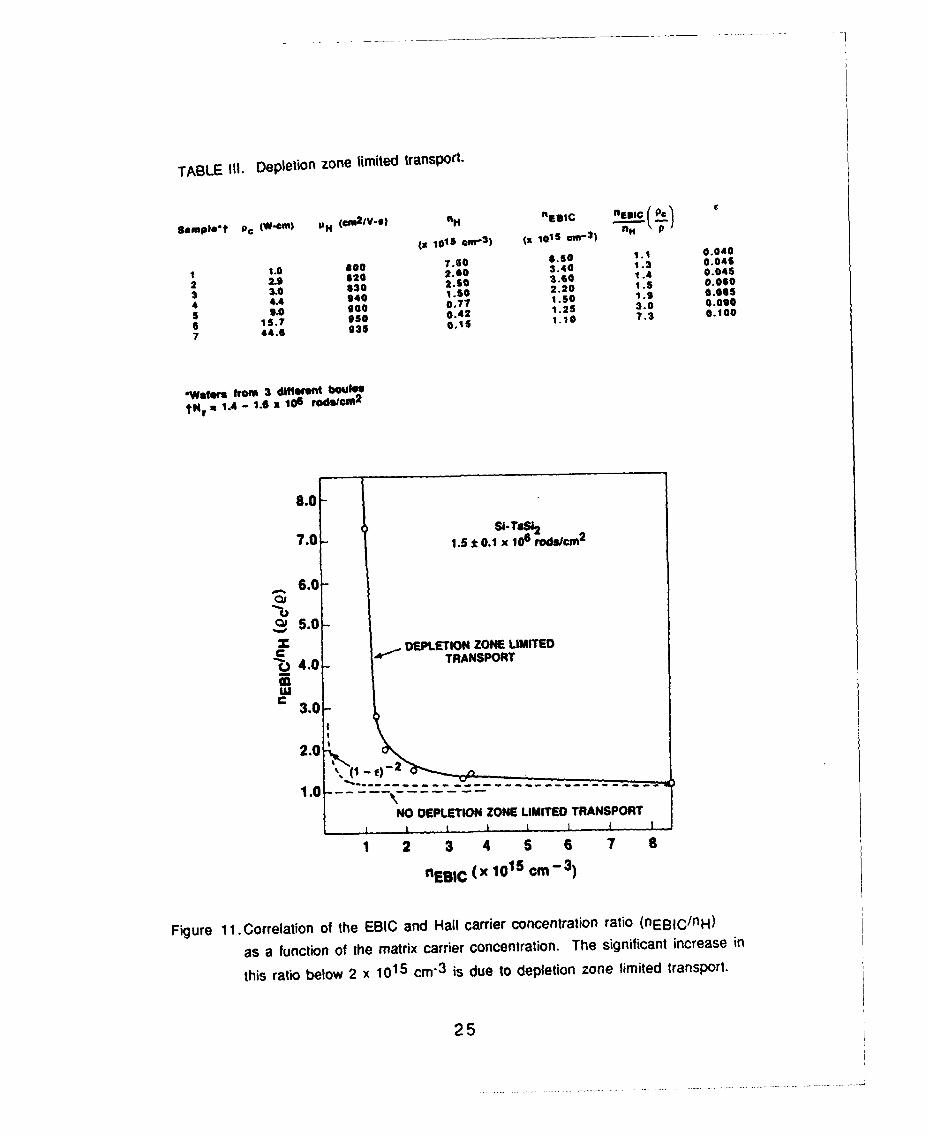
TABLE Ill. Depletion zone limited transport.
s~male't p= (w-1f) ga (Cn nIVl n "IC PC
(P 101 5r3 ) (n t0I5 cm.-3
.0 400 7.0+0 8.50 1.1 0.040
2 1. 20 2.60 3.40 1.3 0.045
23.0 30 2.50 3.60 1.4 0.0454 3.0 40 1.SO 2.20 1.5 0.060
1. 040 o.0 1.50 1.9 0.0054 15.7 0 0.42 1.25 3.0 0.0907 44.6 950 0.15 1.10 T.3 0.100
"Wg~em" fomn 3 dt"Wmt I)QuI"
tN r 1A - 1.6 x Iof rodIcm2
8.07. 5 SI-Tas% i 2
7.0- 1.5 10.1 x 10⁶ rodscm2
6.0
,5 5.0DEPLETION ZONE LIMITED
4.0- TRANSPORT
3.0
2.0'
1.0
NO DEPLETION ZONE LIMITED TRANSPORT
J, I, 1, -, - 1 .1 . .
1 2 3 4 5 6 7 8
nEBIC (x 1015 cm - 3 )
Figure 11.Correlation of the EBIC and Hall carrier concentration ratio (nEBIC/nH)
as a function of the matrix carrier concentration. The significant increase in
this ratio below 2 x 1015 cm-3 is due to depletion zone limited transport.
25

5. EUTECTIC COMPOSITE TRANSISTORS
5.1 Transistor Design and Fabrication
Eutectic composite transistors have been designed and fabricated using a basic concentric
ring design. The outside and inside ring constitute the source and drain, respectively, so that
current must pass under the central ring gate contact. Thus, biasing the gate enables
expansion of the depletion zones in this region and current 'pinch-off.
Ohmic and gate ring contacts were made essentially the same way as the comparable diode
contacts. A quarter section of the surface contacts of a typical device is shown in Fig. 12. As
will be explained in a later section, characterization of transistors made it clear that
divergence of the rods under the ohmic contacts limited blocking voltage. Contacts were
developed that resolved these issues by forming source and drain surface films that contacted
the matrix Si only and not the metallic rods. A schematic of the process is shown in Fig. 13.
For this contacting procedure, the rods within the ohmic contact rings are etched back just
over 1 jim. The cylindrical areas are refilled with resistive polycrystalline Si by a CVD
process. The excess Si coated on the wafer surface is removed in a planarization process.
Following this, the wafer may be processed as a virgin wafer using the CoSi2 /n+ process for
ohmic contacts. The surface silicide metallization contacts either the conducting matrix Si or
the resistive polycrystalline Si, without reaching the recessed TaSi 2 rods. Devices made
using this contacting process, did display comparably low surface resistance, but further
evaluation will be required to determine if it elevates the blocking voltage.
5.2 Transistor Characteristics
Understanding the nature of transistor action in eutectic composites and assessing the
implication for high power switching is an important part of this program. In this section,
the basic features of eutectic composite transitors will be reviewed. The use of advanced
characterization and modeling techniques and the first pulsed power tests will be presented
in subsequent sections. The present understanding of eutectic composite transistors and its
potential impact on pulsed power is reviewed in the final section.
26

d _ _ _
0.4 ,im
Figure 12. A quarter section of the concentric ring pattern of source, drain and gatecontacts used to fabricate the transistor.
27

drain contact source contactarea n+ Tatrix area
holes left byeutectic etching
composite
Vsilicide rods
Step 1: Etch back rods in source and drain areas
drain contact source contact
-refill holes with
silicide rods
Step 2: Deposit high resistivity poly Si and planarize
drain metallization source metallizationgate metallization
n- implant
silicide rods
Step 3: Implant into source and drain areas and deposit
-metallizations.
Figure 13. Schematic procedure for fabricating ohmic contacts that are insulated from
the metallic rods of a eutectic composite.
28
An example of the current-voltage characteristics of a eutectic composite transistor with the
drain current plotted against the drain voltage for different gate voltages is shown in Fig. 14.
The device shown blocks 1000 V. The basic characteristics of the device are similar to those
of a conventional metal-semiconductor field effect transistor (MESFET). Both display a
linear region at low voltage and a saturation region at higher voltages. MESFETs also display
a third region, a breakdown region, that is not characterisitic of the eutectic composite
transistor. Studies of these devices have varied the dimensions of the concentric ring
contacts, the thickness of the wafer, and, over a small region, the carrier concentration.
Before a discussion of the effects of these parameters, several points can be made on the
device's basic characteristics.
* The series resistance of the device, taken as the slope of the unbiased curve in the limit of
small drain voltages, is in agreement with the value expected from the composite resistivity
and the device dimensions assuming the entire thickness of the wafer is used for transport.
This and the ability to 'pinch-off' the device verifies that it is indeed a 'bulk' transistor.
. The drain current in the pinch-off condition, defined as that point at which an increase in
the bias voltage does not result in a further decrease in the drain current, varied
significantly from device to device. Minimum drain currents for the pinch-off condition
measured at 200 V were 2% of the unbiased saturation value. Thus, for example, in a device
with a 20 mA saturation current, pinch-off attained with a -12 V bias at a 200 V drain
potential was 400 j.iA. This may be considered high for a Si p-n junction device but,
considering the dimensions of the device and the low height of the Schottky barrier, these
leakage currents are in-line with expectations. In general, transistor leakage currents were
significantly lower than the diode reverse bias currents when compared for similar voltage
and surface contact area.
0 Characteristics of the transistors were also measured as a function of temperature.
Heating devices from 22 C to 75 C severely degraded the device properties as the leakage
current (measured at -12 V gate and 10 V drain) increased by a factor of 17. The increase
can be largely explained by thermal activation over the small Schottky barrier. Higher
Schottky barrier systems would not be expected to be as temperature sensitive.
29
* At sufficiently high drain voltages devices became leaky and broke down. Breakdown was
observed to be catastrophic and destroyed device characteristics. However, device breakdown
was observed at significantly higher voltages than expected for conventional planar devices
when compared at a similar carrier concentration.
The properties of eutectic composite transistors and the realization of their potential for
high blocking voltage became apparent after a study of the effects of device dimensions,
carrier concentration and resistivity on device blocking voltage. Results from this study are
presented in Table IV. For five different devices the table gives the carrier concentration and
resistivity of the wafer, the gate to drain (g-d) distance, the wafer thickness and the voltage
at breakdown, Vmax. Different entries for the same device corresponds to measurements at
different wafer thicknesses. The wafer thickness was found to have a significant effect on the
breakdown voltage. The device labeled SiTa 61 #25 illustrates the effect. Measurement of
the device on the original 500 Im thick wafer indicated catastrophic failure at 50 V.
Exceeding 50 V on the drain resulted in a loss of the characteristics. After thinning the wafer
from the side opposite that with the surface contacts, the same device was retested. Thinning
the wafer to 250 g~m resulted in recovery of the device. Retested the device yielded similar
characteristics with half the original saturation and current and a breakdown voltage of 350
V. Thinning the wafer further to 125 jim, and retesting yielded another halving of the
saturation current and a new breakdown voltage of 600 V. This value is at least three times
the blocking voltage of a conventional planar device in a wafer of the same 3 x 1015 cm-3
carrier concentration.
The data in Table IV also shows that the breakdown voltage increases with the gate-to-drain
spacing. This observation and the thickness effect indicates that devices breakdown via a
'punch-through' mechanism. In this mechanism, failure occurs when the depletion zone
extends to the drain. A model, schematically illustrated in Fig. 15, based on this failure mode
can be used to explain both the thickness and the gate-to-drain spacing effects. SEM
longitudinal micrographs and EBIC both reveal that some rods are misaligned. Maximum
misalignment has been measured to be 60 relative to crystal axis (or wafer normal). Thus,
as shown in the figure, assuming maximum misalignment, separation of the gate and drain
contacts, as they are extended by contact to the rods, is dependent on the wafer thickness.
When the surface gate-to-drain spacing is 140 ipm, at the bottom of a 500 p.m thick wafer
30

Figure 14.The transfer characteristics of a Si-TaSi2 eutectic composite transistor that
blocks 1000 V.
Table IV. Factors Affecting the Maximum Blocking Voltage
Carrier Concentration Resistivity g-d Distance Thickness Vmax
Wafer (1015) (0-cm) (Pm) (tAm) (V)
SiTa 61 #25 3 8 137 500 50
SiTa 61 #25 3 8 137 250 350
SiTa 61 #25 3 8 137 125 600
SiTa 61 #41 2 12 150 500 90
SiTa 61 #41 2 12 150 250 250
SiTa 61 #41 2 12 150 125 500
SiTa 59 #31 I 18.5 180 250 500
SiTa 59 #31 I 18.5 180 125 700
SiTa 59 #47 I 50 62 250 4)
SiTa 68 #9 I 18.5 250 125 1000
31

(g-d)0 =140 pm
GATERAIN WAFER THICKNESS
(g-d)l
- -_ ___ -125 gim
(g-d) 2
250 gim
____ 500 gim
(g-d) 3 40 9iM
Figure 15. A schematic model showing how the effective gate to drain distance changesas a function of wafer thickness due to rod divergence.
32

the effective separation of the gate from the drain is only 40 pgm. Similarly for a 250 g±m
wafer thickness, the separation is only 90 p.m and so on.
5.3 EBIC Characterization
Conventional electron-beam-induced current (EBIC) techniques applied to the
characterization of eutectic diodes have been used to obtain graphic images of the depletion
zone around a TaSi2 rod and have enabled a quantitative determination of the Si matrix
carrier concentration. The EBIC technique played an important role in diode evaluation.
During the latter part of this program, experimentation began on the development of a new
three terminal EBIC technique which may be as important for transistor devices as
conventional EBIC has been for diodes. Both techniques involve the generation of scanning
electron microscope images which show perturbations of device operation due the electron-
hole pairs created by the electron beam incident on the sample. In conventional EBIC, a
signal corresponding to the the current collected in a diode junction is used to form the image.
It allows the visualization of the depletion regions and relative minority carrier collection
efficiency of the junction rods in these devices. An image showing the annular depletion zones
around the TaSi2 rods was shown in Fig. 10. This technique graphically confirms the basis of
transistor action in these devices, and gives additional information on uniformity of material
and device characteristics.
I The new three terminal technique uses the electron beam generation of electron-hole pairs to
alter the local electric fields in the current channels of the device. The beam-generated
carriers will tend to momentarily reduce any potential differences and electric fields. As a
result, depletion widths in the gate region will decrease, thereby increasing the drain
current. In these SME transistors, this effect is only pronounced at partial pinch-off in
regions where current crowding occurs due to velocity saturation of the carriers. This
j technique can therefore be used to visualize the location and extent of current crowding in
different regimes of device operation by recording images as a function of gate and drain
j voltage. Information can therefore be gained on the characteristics and uniformity of the
transistor effects in different areas of the device.
To implement this technique, we have devised a common-source circuit (Fig. 16) where the
33

I
current amplifier is placed so that the gate current, due to the conventional EBIC effect, and
the drain current have opposite polarities, and so yield opposite contrast and can be
u.stinguished. Fig. 17 shows a three-terminal EBIC micrograph of a eutectic composite
transistor. The gate depletion zones are imaged as lighter contrast, and current crowding in
areas of excess current flow is imaged as dark regions extending from the gate towards the
drain.
This technique, still in its infancy, promises to be very important for understanding current
I voltage and breakdown characteristics. As indicated above the depletion zones extending from
the gate are imaged as the light region in Fig. 17. The ablility to follow the extent of the
depletion zone enables comparison with models and may provide important data on theories of
breakdown. The dark image areas indicate high current flow and represent areas of
nonuniformity which may play an important role in surface breakdown phenomena. In both
cases with additional work, the three terminal EBIC technique may provide the needed
experimental verification of the results of numerical modeling of eutectic composite
transistors.
IIVG GI G
I l
I
Figure 16. The circuit diagram used for the three terminal EBIC technique.
34
I- i l i• i= I w
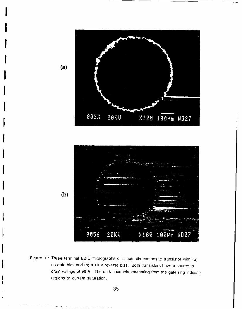
iIII
(a)
I
(b)
Figure 17. Three terminal EBIC micrographs of a eutectic composite transistor with (a)
no gate bias and (b) a 10 V reverse bias. Both transistors have a source to
drain voltage of 90 V. The dark channels emanating from the gate ring indicate
regions of current saturation.
35

5.4. Modeling of Transistor Characteristics
Numerical modeling studies of SME transistors were undertaken both to determine the effects
of device and material parameters on transistor performance and to understand the origins of
their unusual resistance to avalanche breakdown. Computer simulations were performed
using the PISCES code. The PISCES software models two-dimensional distributions of
potential and carrier concentrations for arbitrary device geometries and bias conditions. The
version used was PISCES-IB of Stanford Electronics Laboratories on a Digital VAX 11/785
mainframe computer.
One unique feature of these devices is that the TaSi2 rods which lie between the source, gate,
and drain contacts are not electrically contacted. These rods and their associated depletion
regions float to potentials that are determined by the device parameters and external
voltages. We have performed extensive numerical simulations to study the effects of the
floating rods in high voltage operation, and have shown that they are responsible for the
striking breakdown resistance of SME transistors.
Two types of simulation experiments were performed. In the first, the effect of floating
junctions on device breakdown was studied. The second was aimed at optimizing material and
device parameters for pulsed power applications.
Two basic simulation geometries, shown in Fig. 18, were compared to study the effects of
floating junctions. The conventional case, used as a control (left diagram), has one gate
junction close to the source. The other case (right diagram) has six equally spaced floating
rod-shaped junctions between the gate and drain. With six floating junctions, the simulation
uses the maximum number of electrodes that can be handled by the PISCES software.
Simulations were specified for n-type Si with uniform impurity concentrations of 0.5 - 5 x
1015 cm-3. PISCES-lIB allows the placement of a simple lumped resistance on a givenelectrode. This capability was exploited to account for floating rods, which were simulated
by inserting the maximum allowable resistance (1031 Q) on the floating rods and biasing
them to the drain.
To simulate the operation of the transistor, the source was held at 0 V, the gate electrode (the
36

first rod) was biased to -2 V, and the drain electrode was stepped from 0 to 200 V in 10 V
increments. The potential versus distance from the source is shown in Fig. 19 and the
maximum electric field versus drain potential is shown in Fig. 20 comparing the two cases
with and without floating rods.
For the conventional case without floating junctions, the potential increases parabolically
with distance similarly to conventional planar junctions. The maximum electric field
increases monotonically with increasing drain voltage. In the case with floating rods, the
depletion zone at the gate rod expands with increasing voltage as in the conventional case, but
only until it intersects the depletion zone of the first floating rod. This latter rod then floats
in potential with further increases in applied voltage so that its depletion zone expands
towards the next floating rod. In this way, the applied voltage is spread across successive
floating rods. The electric field at the gate rod reaches a maximum when the drain voltage is
sufficient to extend its depletion zone to the first floating rod. It is then clamped at this value
as the drain voltage is increased. Eventually, the same maximum field is attained at the first
floating rod, and so on. The actual value of this field depends on the interrod spacing and the
carrier concentration, but by proper design it can be made lower than the avalanche field.
The results of this model clearly indicate that the floating rods inhibit avalanche breakdown
and result in a larger depletion zone than would be found in a classical planar junction device.
In a conventional device without floating rods, the maximum electric field increases as the
drain voltage increases until it reaches the critical value for avalanche breakdown. With the
floating rods, however, as the drain voltage is increased the field reaches a maximum that
may be significantly lower than the critical field for avalanche breakdown. Thus, even as the
drain voltage is increased to a value significantly beyond that required to yield avalanche
breakdown in a conventional device, avalanche breakdown is avoided because the field never
reaches a value sufficient to cause impact ionization. However, avalanche will eventually
occur by a 'punch-through' mechanism when the depletion region expands to reach the drain
contact and no additional floating rods are available to accommodate further voltage increases.
Figure 21 shows how the electric field increases after punch-through of the depletion zone to
the drain in a small gate-to-drain distance device. Therefore, the maximum blocking voltage
of the device is determined by the gate-to-drain spacing, rather than the carrier
concentration as in conventional devices. This distance can in principal be designed to yield
37
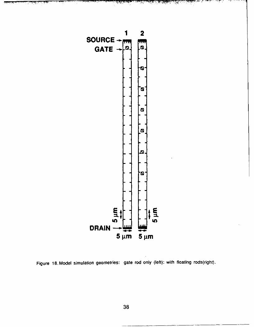
12SOURCE -*
GATE-
Ew
DRAIN -- w~
Figure 18. Model simulation geometries: gate rod only (left): with floating rods(right).
38
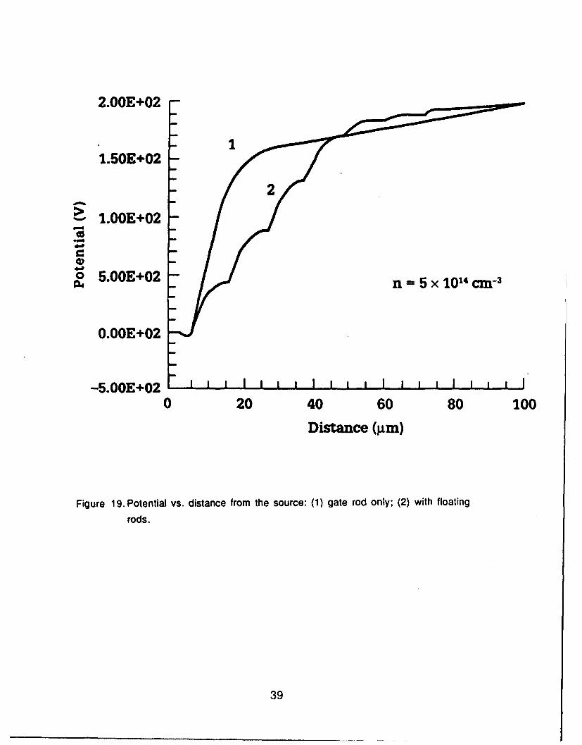
2.00E+02
1.50E+02
1.00E+02
O 5.00E+02 n5 X 1014 CM73
0.00E+02
-5.00E402 II I IIIIIII0 20 40 60 80 100
Distance (grn)
Figure 19. Potential vs. distance from the source: (1) gate rod only; (2) with floating
rods.
39

I ow
I 0
0
2 0 0
0 CCD
U)
400
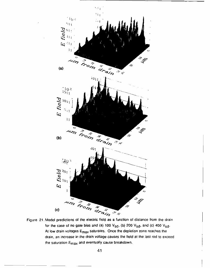
I.t
(a)
(c) Q •
"ro
Figure 21. Model predictions of the electric field as a function of distance from the drain
for the case of no gate bias and (a) 100 Vsd, (b) 200 Vsd, and (c) 400 Vsd.At low drain voltages Emax saturates. Once the depletion zone reaches the
drain, an increase in the drain voltage causes the field at the last rod to exceed
the saturation Emax and eventually cause breakdown.
41

an arbitrarily large blocking voltage.
Further model calculations were used to investigate the ways that these devices could be
optimized for simultaneous high voltage and high current operation. This was done by
calculating the carrier concentration required to hold the maximum electric field to a given
value less than that of the avalanche field for different interrod spacings. The saturation
current density in each case was also determined. A microstructure with floating rods
similar to that shown in Fig. 18 was modeled to determine the carrier concentration which
yields a saturation Emax of 100 kV/cm. This maximum field was chosen because it is
conservatively below the value that would lead to avalanche breakdown. The average electric
field in the gate-drain region and the gate-drain distance needed to hold off 1000 V were also
calculated. The microstructure was then scaled uniformly to different interrod spacings and
rod diameters, keeping the volume fraction of the rods constant (as would be the case with
real eutectic systems).
Table V. Model calculations of SME transistor parameters forcombinations of carrier concentration and interrod spacing that will yielda maximum electric field of 100 kV/cm.
Rod Avg. Field G-D distanc ND Js
spacing at Emax for VSD=1 000 V
4 p.m 5.08x10 4 V/cm 200 pn 5.9x10 1 5 cm- 3 6500 A/cm 2
7 5.37x0 4 186 3.3x1 0 1 5 3300
23 5.44x0 4 184 1.0x1 0 1 5 870
The results are shown in Table V for interrod spacings of 4, 7, and 23 g~m. Although the
gate-to-drain distances needed to hold off 1000 V are similar in all three cases and the
spatially averaged field remains nearly constant at about one-half Emax, the carrier
concentrations and saturation current densities at zero gate bias are quite different. The
highest current is found at the smallest interrod spacing. The conclusion from these
modeling studies is clear. Eutectics with higher rod density should be able to switch much
higher currents than low rod density devices because of the higher matrix carrier
42

concentration without a degredation in the maximum hold-off voltages. In principle, then,
eutectic composite transistors should be able to switch high voltages and high currents.
5.5 Pulsed Tests
Throughout the program, transistor characterization has been done using curve tracers in an
essentially dc mode. At the high voltage, high current range, dc testing lead to some device
heating. For this reason, and because the ultimate application of these devices is in pulsed
applications, high voltage devices were prepared for pulsed testing. Devices with dimensions
designed to hold-off 2000 V (assuming that the average field between gate and drain must be
less than 50 kV/cm) have been processed and subject to an initial test. The high voltage
properties were tested using a high voltage gas discharge apparatus schematically illustrated
in Fig. 22. This equipment is capable of delivering 100 ns pulses of 2 - 10 kV.
A preliminary measurement on a device shows breakdown at lower than the intended 2000 V
and passage of 5 A of current. The test is an indication that at these high voltages, surface
breakdown may limit the device. Because the TaSi2 rods extend through the thickness of the
device, the applied potentials appear at both top and bottom surfaces, as well as in the
interior. This suggests that surface passivation of both surfaces may be required before
testing. Surface breakdown issues will have to be examined in future studies.
43

UV FLASH ,,,,\ I / TRIGGER
--RIGG-- DIGITIZING
VOLTAGE PROBE SCOPE
CHARGING VGLINE
HV> i EL___/ D.U.T. DIGITIZING
SCOPEFORMING GAP
Figure 22. Schematic diagram of the high voltage plasma discharge apparatus.
44

6. IMPLICATIONS OF PULSED POWER
Semiconductor-metal eutectic composites offer many intriguing opportunities for pulsed
power devices. Experimentally, the maximum hold-off voltage demonstrated to date is 1000
V, but all the experimental and theoretical studies derived in this program indicate that
significantly higher voltages could be handled, and most importantly, that eutectic composite
devices should be possible that can hold off substantially higher voltages than conventional
planar junction devices. According to the model and experimental support attained to date, a
50 kV device can be made if the gate to drain spacing is maintained at 1 cm.
Achievement of high current also appears to be possible with eutectic composite devices.
Assuming a 1 in diameter wafer, which is typical of those currently grown, and achievement
of about 100 A/cm2 , which is typical of current devices, efficient use of chip space in a
device with a 0.2 cm gate-to-drain spacing to derive a 10 kV hold-off voltage would enable
switching of about 50 A. Development of techniques for growing 2 in diameter composite
boules, would yield 200 A. Orders of magnitude improvement could be obtained if the
current density were increased. Modeling suggests that development of eutectic composite
with finer interrod spacings could yield the substantial current increases desired and, thus,
also points to the need for continuing studies of new materials systems and factors that affect
the interrod spacing in known systems.
Progress towards demonstration of higher voltage, higher current devices will require
continued work on the dual research fronts of materials and devices. With the currently
available material, devices can be envisioned that can block high voltage and switch high
currents. High current switching depends on fabrication of large area devices or connecting
large devices in parallel. This may impose stringent demands on structural uniformity of the
Si-TaSi2 material. Observations on device yield within a wafer have not indicated any
correlation with device size, but since all devices on a given wafer are not active, that is
yield per wafer is not 100 %, building devices that cover an entire wafer may undergo yield
limitations.
Increases in current switching beyond that possible with large area devices can result from
the development of new materials. This program has pointed towards the need for materials
45

with better alignment of rods to enable use of thicker wafers, higher barrier heights to
reduce leakage and temperature sensitivity and, most importantly, higher rod density to
allow for higher carrier concentration.
Since the devices are intended for pulsed power applications, more work will need to be done
on testing under pulsed conditions and, any unexpected limitations imposed by this should be
understood using modeling techniques. This is one aspect of this research that must be
expanded.
Furthermore, the concept of floating junctions developed in this work may have implications
for pulsed power devices that go significantly beyond SME devices. Incorporation of floating
junctions to increase the current and voltage capabilities of conventional devices, possible
using advanced processing techniques, holds considerable promise for the general field of
solid-state opening switches.
46

7. REFERENCES
1. B. Reiss and T. Renner, Zeitschrift fur Naturforshung 21, pp. 546-548 (1966).
2. W. T. Read, Philos. Mag., 46, 111 (1955).
1 3. V. J. Samalam, J. Appi. Phys., 67, 2165 (1990).
I4

I
I A
I
III
Appendix BI Recent Publications
IIIIIIIII

IEEEConference Record of the
1992 TwentiethPower Modulator Symposium
IIII

HIGH VOLTAGE SEMICONDUCTOR.METAL EUTECTIC
TRANSISTORS FOR PULSED POWER SWITCHING APPLICATIONS
0V. Nguyen. P R. Rossoni. M. Levinson and B-M Ditchek
GTE Laboratories Inc., Waltham. MA 02254
Abstna=
High power transistors for pulsed power switchingapplications based on semiconductor-metal eutectic(SME) composites are described. Experimental deviceswith 6 kV blocking voltage have been demonstrated. Theability to parallel devices for higher currents has also OATINGbeen demonstrated. In addition, transient simulations and SOURCE GATE JUNCTIONS DRAINspeed measurements have shown fast opening switch 1capacity with response times of less than 15 ns.
Using conventional transistor technology for pulsed power S MATRI T.51 2 FIBERSswitching would reqiure the development of devices withhigh on-state current and high blocking voltage. The mainobstacle for devices to block voltages in excess of I kV is Fig. 1. SME transistor geometry.avalanche breakdown. Avalanche breakdown occurswhen carriers overcoming the barrier at the gate gain Figure 2 shows a typical transfer characteristic of a SMEsufficient energy when accelerated by the large electric device. The basic characteristics of the device are similarfield in the depletion zone to cause multiple ionization of to those of a conventional MESFET in that they display abound charge carriers. The maximum breakdown voltage linear region and a saturation region. For high poweris determined by carrier concentration. A low carrier applications, the resistance should be small, theconcentration is needed for high blocking voltage, which saturation current should be large and the hold off voltagehas an adverse effect on the on-state current. This should be as high as possible.breakdown mechanism together with basic junctionphysics limits conventional devices with reasonable sizeto high voltage or high current but not both.
Semiconductor-metal eutectic (SME) composites Per Vert.represent a new class of electronic materials which have DMsion 5 mAa very unique microstructure. These materials containarrays of micron-sized metallic rods imbedded in a single Per Horz.crystal semiconductor matrix. They are formed directly Division 20 Vduring the crystal growth process from the melt. The rodsform parallel, cylindrical Schottky junctions with the Per Step 2 Vsemiconductor and provide the basis for novel electronicand opto-electronic devices, especially high power g. Pertransistors. Performance exceeding that of conventional Division 2.5 mSdevices has been demonstrated in SME materials basedon the Si-TaSi2 system [1,2).
In this paper, state-of-the-art SME devices will bedescribed and the effect of composite microstructure on Fig. 2. Characteristics of a Si-TaSi2 SME transistor.the properties of the devices will be discussed. Inaddition, the speed measurements will also be presented.
Device properties and discussions
Device fabrication and characteristics ggrjo
The device geometry is shown in Fig 1. A standard Transfer characteristics of a SME transistor designed withconcentric ring structure was used to fabricate transistors. the gate-drain distance of 500 ILm are shown In Fig. 3. AA CoSi2 film was used for all contacts. Ohmic contacts at blocking voltage of 2.2 kV was demonstrated. This highthe source and drain were formed with As+ Implants. blocking voltage is remarkable when It Is compared withRectified gate contacts were formed with B+ Implant. the 0.3 kV maximum breakdown voltage expected for aMore detailed information on processesing can be found conventional Si device with the same carrierelsewhere (3]. concentration of 1015 cm- 3 based on an avalanche
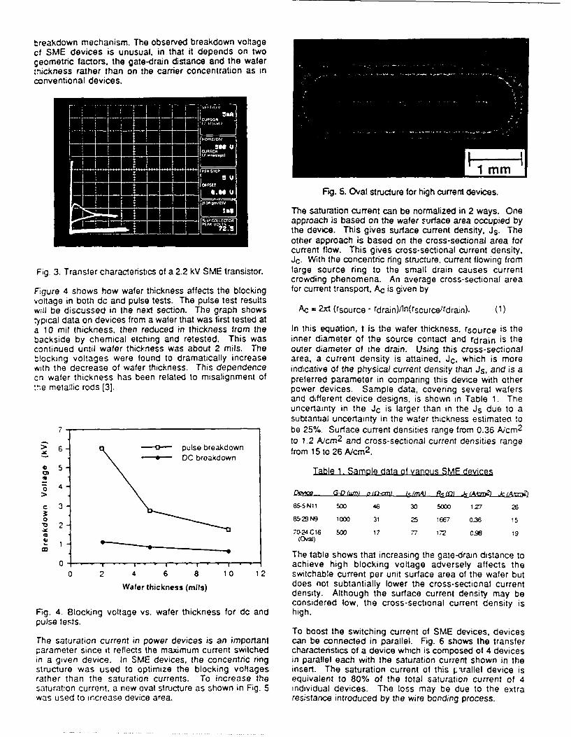
breakdown mechanism. The observed breakdown voltagecf SME devices is unusual, in that it depends on twogeometric factors, the gate-drain distance and the wafer:nickness rather than on the carrier concentration as inconventional devices.
mmhimmi*II* *IIII* Fig. S. Oval structure for high current devices.*EMmmmmmm The saturation current can be normalized in 2 ways. Onemmm approach is based on the wafer surface area occupied by
the device. This gives surface current density. Js. Theother approach is based on the cross-sectional area forcurrent flow. This gives cross-sectional current density.Jc. With the concentric ring structure, current flowing from
Fig. 3. Transfer characteristics of a 2.2 kV SME transistor. large source ring to the small drain causes currentcrowding phenomena. An average cross-sectional area
Fgure 4 shows how wafer thickness affects the blocking for current transport, AC is given byvoltage in both dc and pulse tests. The pulse test resultswill be discussed in the next section. The graph shows Ac = 2xt (rsource - rdrain)/ln(rsource/rdrain). (1).ypical data on devices from a wafer that was first tested ata 10 mil thickness, then reduced in thickness from the In this equation, t is the wafer thickness, rsource is thebackside by chemical etching and retested. This was inner diameter of the source contact and rdrain is thecontinued until wafer thickness was about 2 mils. The outer diameter of the drain. Using this cross-sectional,locking voltages were found to dramatically increase area, a current density is attained, Jc, which is morewith the decrease of wafer thickness. This dependence indicative of the physical current density than Js, and is acn wafer thickness has been related to misalignment of preferred parameter in comparing this device with other:ne metallic rods [3]. power devices. Sample data, covering several wafers
and different device designs, is shown in Table 1. Theuncertainty in the Jc is larger than in the Js due to asubtantial uncertainty in the wafer thickness estimated to
7- be 25%_ Surface current densities range from 0.36 A/cm 2
6 ato 1.2 A/cm2 and cross-sectional current densities range6p breakdown from 15 to 26 A/cm 2 .
c - Table 1 Samole data of various SME devices0 4
> Device G-D (um) 0 .l-aT) 4 IrAi 1-(n) A tSj~ 4 &Aj i
c 3 85--5 N1 500 46 30 5000 127 250 5N9 1000 31 25 1667 036 15
'a 27024CI6 500 17 77 172 0-% 19
The table shows that increasing the gate-drain distance to0 ,......... ................ achieve high blocking voltage adversely affects the
0 2 4 6 8 1 0 12 switchable current per unit surface area of the wafer butWafer thickness (mils) does not subtantially lower the cross-sectional current
density. Although the surface current density may beconsidered low, the cross-sectional current density is
Fig. 4. Blocking voltage vs. wafer thickness for dc and high.pulse tests.
To boost the switching current of SME devices, devicesThe saturation current in power devices is an important can be connected in parallel. Fig. 6 shows the transferparameter since it reflects the maximum current switched characteristics of a device which is composed of 4 devicesin a given device. In SME devices, the concentric ring in parallel each with the saturation current shown in thestructure was used to optimize the blocking voltages insert. The saturation current of this i':rallel device israther than the saturation currents. To increase the equivalent to 80% of the total saturation current of 4saturation current, a new oval structure as shown in Fig. 5 individual devices. The loss may be due to the extrawas used to increase device area. resistance introduced by the wire bonding process.

60 An example of the voltage waveform with the automotive
coil is shown in Fig. 8 as a 1000 p~m gale-drain distanceso SME device is tested. The device is clearly demonstrated
to support a full 6 kV. Above 6 kV the device breaksZdown. indicating that 6 kV for this device is the maximumE blocking voltage. During high voltage testing, wafers
1were immersed in transformer oiL Without transformer oilarcing occurs and damages devices under test.
10- -TO- 65 MA ,
vollg ,) 7 4-
Fig. 6. Transfer characteristics of a parallel device. -
This result indicates that the fabrication of large current 2: I
switching devices, as well as high blocking voltage .i.
devices will be possible through the paralleling technique. V i
Table I also shows the series resistance for each device. ocalculated as the ratio of 50 mV with the drain current at -50 mV. This may be compared with the expected -20 S 10 15 20resistance based on tie resistivity measured for the Tim* (10 Sec)particular wafer and the effective cross-sectional andlength of transport. When the comparison Is made for Fig. 8. Voltage waveforms of a SME transistor underthese 2 mils thick devices, agreement Is excellent, pulsed test. The solid line shows a full 6 kV waveformindicating that the contacts are good and that the entire supported by the device. Above 6 kV. device breakswafer thickness is being utilized as the current channel down as shown by the dashed line.
Pulseoration The effect of wafer thickness on the breakdown voltage inpulsed tests is shown in Fig. 4. As in dc tests, the
Pulse tests on SME dev;,ces were performed with the two breakdown voltage increases as the thickness decreases.circuits shown in Fig.7. The highest voltage pulses weregenerated with the spark coil circuit shown in Fg. 7a with In the pulsed tests described above, the SME transistoreither a 4 kV Xenon flash coil, which generated a 700 ns assumes a passive role, however, using the circuit in Fig.wide pulse, or a 25 kV automotive spark coil, which 7b. the high voltage pulses can be generated using thegenerated a longer 80 ps pulse. These tests were switching capability of the transistor tself. By passing aperformed with the gate of the transistor shorted to the current through an inductor and test transistor connecteddrain, so that maximum saturation currents flowed through in series, the magnetic field stored in the inductor isthe transistor during pulse testing. converted into a high voltage pulse at the drain of the
transistor as the transistor is switched from the on-stale to4kV xenon flash coil the off-state by the -10 V output of the pulse generator.or 2Skv automotive The pulse generator has a 6 ps wide pulse and a 20 nsspark coil Transistor rise and fall time.
300V 0C under test
Oscillo -_ _ _ _ _ _ __ _ _ _ _ _ _
-, I I I v 57 0.6oSscopeV 0.6..120
-- C, -
--0.4
s
43rH Pulse I- 040
Inducto GeneratorlO - ;2 - s~m..~t r +t - I ...................
l-0A - Os cilo- TransistorDC current ___soev under test I0 vQ Oscillo-
supply scope > 0 -400 2 4 6 8 10
Time (jiS)
Fig. 9. The sold line is a voltage pulse generated with the
Fig. 7. (a) Spark coil dicuit for high voltage pulse test and inductive circuit using a SME transistor. The dashed line(b) Inductive circuit for high voltage and high current pulse is a current pulse.

A voltage pulse generated with this circuit using a 10 milthick SME transistor is shown in Fig. 9. The pulsegenerator results in the switching of 60 mA and the Transistors fabricated from SME materials have beengeneration of a 0.5 kV pulse within 5 lis for the pulse. To shown to possess properties suitable for pulsed powermeasure current pulse, a 10 Q resistor is connected in applications. Blocking voltage up to 6 kV. moderateseries to the source and the oscilloscope is set to track the. current density up to 26 A/cm2 and rapid opening times.voltage drop across the resistor as shown in Fig. 7b. The less than 15 ns, have all been demonstrated. Based oncurrent waveform is also shown in Fig. 9 and an these performance parameters, SME devices should takeexpansion of the time scale at the switch opening portion their place among other high power devices, includingis shown in Fig. 10. The current drops from maximum to SITs, MOSFETs and Thyristors.minimum value in approximately 15 ns. Therefore, theopening time of the switch has been shown to be 15 ns orless. Acknowiedements
Technical assistance of Mr. T. Middleton in the crystal
80 .growth and device processing is greatly appreciated. Thiswork was supported in part by the Strategic DefenseInitiative Office/Innovative Science and Technology(SDIOAST) and managed by the Office of Naval Research
4 0under contract N0001 4-86-C-0595.-40
C~References
0 1) B.M. Ditchek, T.R. Middleton, P.G. Rossoni and B.G.o 0 Yacobi, *Novel high voltage transistor fabricated using the
0 in situ junctions in a Si-TaSi2 eutectic compositeo, Appl.(I) Phys. Lett. 52. 1147 (1988).
-40 . . 2) B.M. Ditchek and B.G. Yacobi, "Semiconductor-metaleutectic composites for high power switchingo, SPIE
a 1 0 20 30 40 50 Space Structure. Power and Power Conditioning 871,148 (1988).
Time (ns) 3) B.M. Ditchek and B.G. Yacobi, "Microcharacterization
and novel device applications of semiconductor-metalFig. 10. Current waveform at switch opening portion in eutectic composites-. Jpn. J. Appl. Phys. 27, L2155Fig. 9 with the time scale expansion. (1988).
Proceedings of the
FOURTH SDIO/ONR PULSE POWERMEETING 1991
June 20-21, 1991
University of Southern CaliforniaLos Angeles, CA 90089-0484
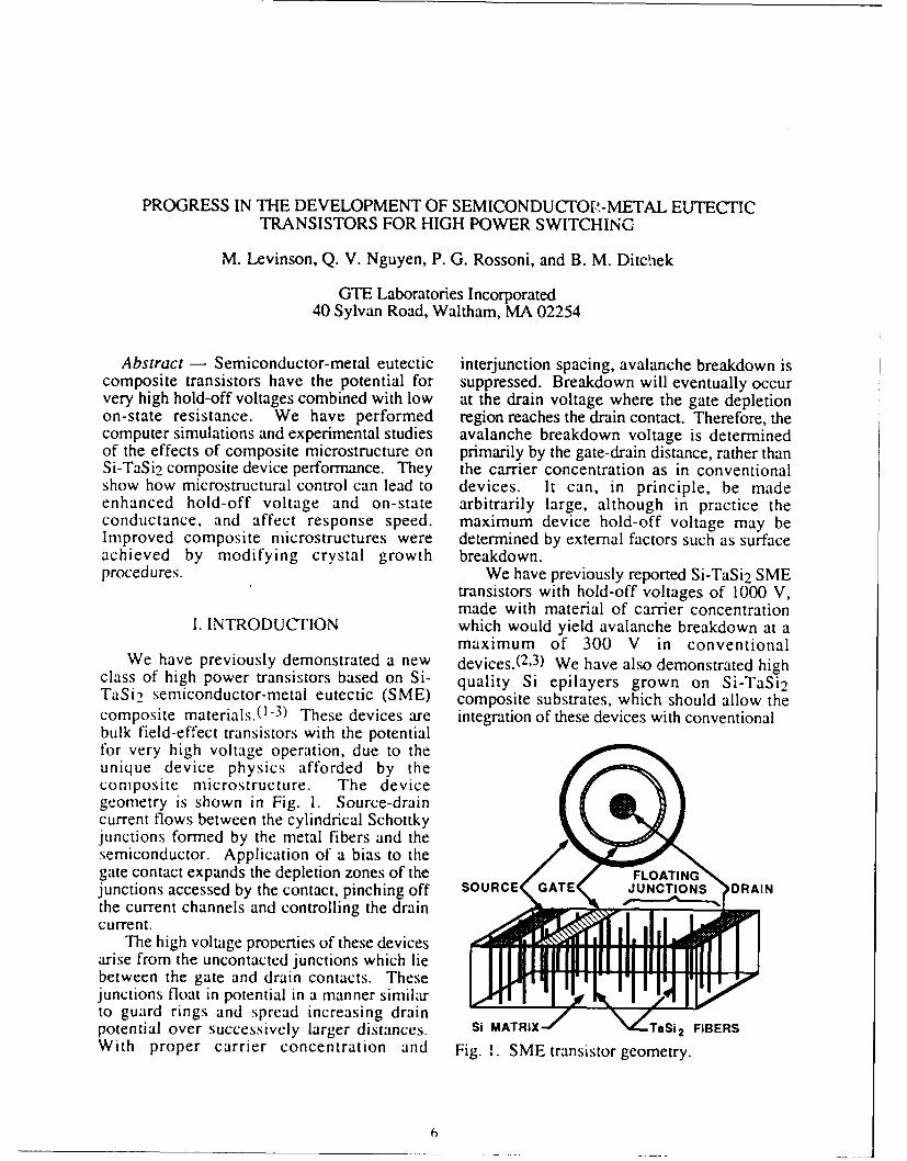
PROGRESS IN THE DEVELOPMENT OF SEMICONDUCTOP-METAL EUTECIC
TRANSISTORS FOR HIGH POWER SWITCHING
M. Levinson, Q. V. Nguyen, P. G. Rossoni, and B. M. Ditchek
GTE Laboratories Incorporated40 Sylvan Road, Waltham, MA 02254
Abstract - Semiconductor-metal eutectic interjunction spacing, avalanche breakdown iscomposite transistors have the potential for suppressed. Breakdown will eventually occurvery high hold-off voltages combined with low at the drain voltage where the gate depletionon-state resistance. We have performed region reaches the drain contact. Therefore, thecomputer simulations and experimental studies avalanche breakdown voltage is determinedof the effects of composite microstructure on primarily by the gate-drain distance, rather thanSi-TaSi2 composite device performance. They the carrier concentration as in conventionalshow how microstructural control can lead to devices. It can, in principle, be madeenhanced hold-off voltage and on-state arbitrarily large, although in practice theconductance, and affect response speed. maximum device hold-off voltage may beImproved composite microstructures were determined by external factors such as surfaceachieved by modifying crystal growth breakdown.procedures. We have previously reported Si-TaSi2 SME
transistors with hold-off voltages of 1000 V,made with material of carrier concentration
I. INTRODUCTION which would yield avalanche breakdown at amaximum of 300 V in conventional
We have previously demonstrated a new devices.(2 ,3) We have also demonstrated highclass of high power transistors based on Si- quality Si epilayers grown on Si-TaSi 2TaSii semiconductor-metal eutectic (SME) composite substrates, which should allow thecomposite materials.(1 -3) These devices are integration of these devices with conventionalbulk field-effect transistors with the potentialfor very high voltage operation, due to theunique device physics afforded by thecomposite microstructure. The devicegeometry is shown in Fig. 1. Source-draincurrent flows between the cylindrical Schottkyjunctions formed by the metal fibers and thesemiconductor. Application of a bias to thegate contact expands the depletion zones of thejunctions accessed by the contact, pinching off SOURCE GATE JUNCTIONS DRAINthe current channels and controlling the draincurrent.
The high voltage properties of these devicesarise from the uncontacted junctions which liebetween the gate and drain contacts. Thesejunctions float in potential in a manner similarto guard rings and spread increasing drain N,potential over successively larger distances. Si MATRIX -TaSi2 FIBERSWith proper carrier concentration and Fig. I. SME transistor geometry.
6
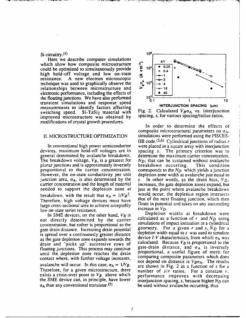
Si circuitry.(4) 108Here we describe computer simulations sir
which show how composite microstructure "scould be optimized to simultaneously provide 0 1 • 0.250 0.4 .high hold-off voltage and low on-state 10 --- 1resistance. A new electron microscopic "" 10 -2a•technique was used to graphically observe the M 10+ -, .4relationships between microstructure and > -16electronic performance, including the effects of 1 40
the floating junctions. We have also performed 1 1J 1 10transient simulations and response speedmeasurements to identify factors affecting INTERJUNCTION SPACING (gim)
switching speed. Si-TaSi2 material with Fig. 2. Calculated VBaA vs. interjunctionimproved microstructure was obtained by spacing, s, for various spacing/radius ratios.modifications of crystal growth procedures. In order to determine the effects of
composite microstructural parameters on GA,
II. MICROSTRUCTURE OPTIMIZATION simulations were performed using the PISCES-liB code.(5,6) Cylindrical junctions of radius r
In conventional high power semiconductor were placed in a square array with interjunctiondevices, maximum hold-off voltages are in spacing s. The primary criterion was togeneral determined by avalanche breakdown. determine the maximum carrier concentration,The breakdown voltage, VB, is a greatest for ND, that can be sustained without avalancheplanar junctions and is approximately inversely breakdown occurring. This conditionproportional to the carrier concentration. corresponds to the ND which yields a junctionHowever, the on-state conductivity per unit depletion zone width at avalanche just equal tojunction area, aA, is also determined by the s. In other words, as the drain bias, VD,carrier concentration and the length of material increases, the gate depletion zones expand, butneeded to support the depletion zone at just at the point where avalanche breakdownbreakdown, with the result that aA 1/VB2 . would occur, the depletion region intersectsTherefore, high voltage devices must have that of the next floating junction, which thenlarge cross-sectional area to achieve acceptably floats in potential and takes on any succeedinglow on-state series resistance, increase in VD.
In SME devices, on the other hand, VB is Depletion widths at breakdown werenot directly determined by the carrier calculated as a function of r and ND usingconcentration, but rather is proportional to the simulations of impact ionization in a cylindricalgate drain distance. Increasing drain potential geometry. For a given r and s, ND for ais spread over a continuously greater distance depletion width equal to s was used to simulateas the gate depletion zone expands towards the device I-V characteristics, from which aA wasdrain and "picks up" successive rows of calculated. Because VB is proportional to thefloating junctions. This process may continue gate-drain distance, and aA is inverselyuntil the depletion zone reaches the drain proportional, a useful figure of merit forcontact where, with further voltage increases, comparing composite parameters which does
not depend on distance is VBCFA. The resultsavalanche will ccur. In this case, ra~ I1/V8 . are shown in Fig. 2 as a function of s for aTherefore, for a given microstructure, there number of sir ratios. For a constant r,exists a cross-over point in VB above which performance improves with decreasingthe SME device can, in principle, have lower interjunction spacing, s, because higher ND cancra than any conventional transistor.(5) be used without avalanche occurring, thus
7

106 microscopic scale because the active junctionseCONVENTIONAL are self-assembled during crystal growth ande r=0.5,s=8 are not as uniform in size, shape, and spacing
104 ---- r=0.2.s=0.4 as those used in the simulation models.Previous studies showed that the spacing and
UwI arrangement of the TaSi2 junctions in actualD 102 materials can have a large effect on currentZ4 transport.(7, 8) Therefore, the optimization ofC. these devices will require a more detailed
100 understanding of the relation between materialz microstructure and device electronic properties.o Recently, we devised a new three-terminal
010-10000 electron-beam-induced conductivity (TTEBIC)technique( 9) which images the microscopic
BREAKDOWN VOLTAGE (V) current characteristics of field-effect transistors
Fig. 3. Optimum areal conductance vs. break- during device operation and shows theirdown voltage for conventional devices and relation to device structure. Image contrast isSME devices with two combinations of junc- generated in the scanning electron microscopetion radii and spacing. using variations of drain current which arise
from electron-beam-induced perturbations of
lowering CA. The optimum sir ratio is about the electric fields within the device. In these2:1. At lower values, GA is reduced by the images, darker contrast indicates areas wheresmaller cross-sectional area of the current the drain current is constricted. The activechannels, while at higher values, a lower ND is areas of gate depletion zones are thus madeneeded to prevent breakdown. visible and can be imaged at different points in
Fig. 3 compares the predicted optimum GA the device I-V characteristic.as a function of VB for two sets of r and s Fig. 4 shows a portion of the gate ring ofvalues and for conventional semiconductor an SME transistor. The electron beam isdevices using planar junctions. For r = 0.5 j.m incident on the surface of the wafer oppositeand s = 8 .m, similar to existing Si-TaSi 2 the contacts, and the drain is to the right of thecomposites, the optimum SME device will have image. Fig. 4(a) shows a conventional chargehigher conductivity than conventional devices collection image of the ends of the TaSi2for VB in excess of -1 kV. For example, aA junctions which are accessed by the gateshould be greater by a factor of -15 for VB = contact. The depletion zones appear as bright10 kV. However, devices made using a annuli around the fibers. In Fig. 4(b) at VG =hypothetical denser composite with r = 0.2 Itm 0 V and VD = 10 V, the dark areas of theand s = 0.4 I.tm could be superior to TTEBIC image show those regions of the gateconventional ones for any VB above - 50 V. In where the current is concentrated. It is seenthis case, GA could be up to -50 times greater that they are not uniformly distributed along thethan in conventional devices-for VB = 1 kV and gate. They appear where the spacing between-1000 times greater for VB = 10 kV. TaSi 2 junctions is greatest. These and other
images show that non-uniformities of fiberdistribution can result in delayed drain current
III. ELECTRONIC saturation (the "knee" of the I-V curveMICROCHARACTERIZATION occurring at higher VD) and excess leakage
current at pinch-off.(9 )In addition to the effects of idealized SME Comparison of Figs. 4(a) and 4(b) also
microstructural parameters, real composites graphically shows the effect of the floatingmay have properties which vary on a junctions. The right-hand dark regions are
8
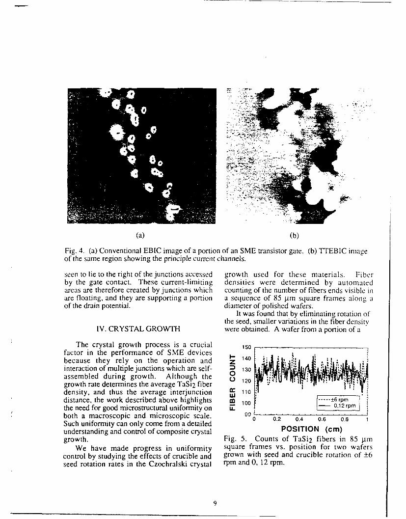
(a) (b)
Fig. 4. (a) Conventional EBIC image of a portion of an SME transistor gate. (b) TTEBIC imageof the same region showing the principle current channels.
seen to lie to the right of the junctions accessed growth used for these materials. Fiberby the gate contact. These current-limiting densities were determined by automatedareas are therefore created by junctions which counting of the number of fibers ends visible inare floating, and they are supporting a portion a sequence of 85 tam square frames aiong aof the drain potential. diameter of polished wafers.
It was found that by eliminating rotation ofthe seed, smaller variations in the fiber density
IV. CRYSTAL GROWTH were obtained. A wafer from a portion of a
The crystal growth process is a crucial 150factor in the performance of SME devices 140because they rely on the operation and z :: , , . .
interaction of multiple junctions which are self- 130assem bled during growth. Although the O 20 : ' "
growth rate determines the average TaSi2 fiberdensity, and thus the average interjunction 110distance, the work described above highlights U1 ± rpmthe need for good microstructural uniformity on E'7 I--both a macroscopic and microscopic scale. 0 0.2 0.4 0.6 0.8 1
Such uniformity can only come from a detailed
understanding and control of composite crystal POSITION (cm)growth. Fig. 5. Counts of TaSi2 fibers in 85 jtm
We have made progress in uniformity square frames vs. position for two waferscontrol by studying the effects of crucible and grown with seed and crucible rotation of ±6seed rotation rates in the Czochralski crystal rpm and 0, 12 rpm.
9

a boule grown with no seed rotation and transit time will decrease significantly as thecrucible rotation of 12 rpm exhibited a mean depletion region collapses back toward the gatefiber count of 127.0 with a standard deviation contact. The rate of this collapse will beof 6.85, compared to one grown with seed determined by the gate-source and gate-drainrotation of 6 rpm and crucible counterrotation capacitances. Thus the turn-on transient mayof -6 rpm, which yielded a mean and standard be slower than that of turn-off, with a timedeviation of 127.6 and 8.40, respectively, constant that would increase with increasingFiber counts vs. position for the two wafers are VD.shown in Fig. 5. There is an additional phenomenon that
Although these measurements are on too may affect the turn-on response of floatinglarge a scale to predict improvements in junction devices. It is commonly observed inindividual device performance by using devices using guard rings.(] 0 ) The floatingmaterial grown without seed rotation, they junctions exchange charge with the bulkwould at the least infer better device yield. semiconductor as their potential shifts. DuringMeasurements of microscale uniformity in this the turn-off process, they float towards thematerial are in progress. drain potential and lose charge by a majority
carrier current to the drain. During turn-on,however, the opposite charging process must
V. TRANSIENT RESPONSE occur by minority carrier current or leakage andis relatively slow. During this time, the
The response speed of SME transistors will depletion zones of the floating junctions arebe affected by transit time delay and parasitic larger than when they are neutral, thuscapacitance and resistance in the same way as constricting the current channel and producingconventional FET's. But a major question is a long time-constant tail to the drain current.how, if at all, these properties will be affected during turn-on.by the floating junctions. The floating PISCES simulations of SME transistorjunctions in SME transistors create a depletion transient behavior illustrate this effect. Fig. 6region whose length varies greatly between the shows the calculated turn-on response of aon-state, where it is simply the length of the model device for VD = 50, 200, and 300 V. Agate contact region, and the off-state, where it constant value of load resistance was used, soextends over a large portion of the gate-drain that the on-state operating point is moving updistance and depends on VD. Therefore, it is the I-V curve with increasing VD. At VD = 50expected that the transit time would differ V, the device is in the linear region in the on-between the turn-on (closing switch) and turn- state, so the gate depletion zones are not greatlyoff (opening switch) processes.
When the device is in the process of turningoff, carriers which have passed through the a" 600
gate contact depletion region will not contribute E soE 300 V
further to transit delays because their motionwill be accompanied by current in the drain 400 2contact. Therefore, the turn-off process should i. 300not be greatly affected by the floating gates, but ,, 200should be governed by parasitic capacitance 0: s0V
W 100and resistance as in conventional metal-semiconductor FETs. o 0 0. 20. 40. 60. 80. 100.120-200 04 60 0I012
During the turn-on process, on the other TIM (48)hand, the first carriers to transit the gate region TIME G's)must pass through the extended depletion zone Fig. 6. Simulated SME transistor turn-onbefore they can force current at the drain. The response for different i'D.
10
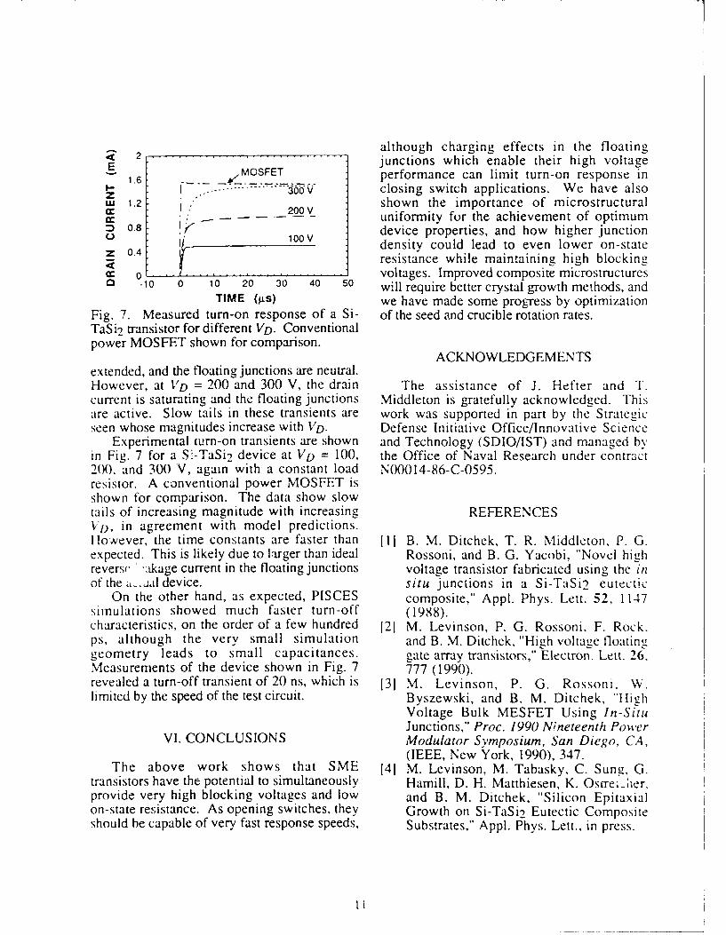
2 although charging effects in the floatingE -- -- junctions which enable their high voltage
6 MOSFET performance can limit turn-on response in1.6.... 0v closing switch applications. We have also
Z 30" lsn wic plcton.W aeas
1.2 - shown the importance of microstructuraln- 200V, 1.2 20 - uniformity for the achievement of optimum
0.8 " device properties, and how higher junction100 .4 density could lead to even lower on-state
Rresistance while maintaining high blockingcc 0 . voltages. Improved composite microstructures0 -10 0 10 20 30 40 50 will require better crystal growth methods, and
TIME (gs) we have made some progress by optimization
Fig. 7. Measured turn-on response of a Si- of the seed and crucible rotation rates.TaSi 2 transistor for different VD. Conventionalpower MOSFET shown for comparison.
ACKNOWLEDGEMENTSextended, and the floating junctions are neutral.However, at VD = 200 and 300 V, the drain The assistance of J. Hefter and T.current is saturating and the floating junctions Middleton is gratefully acknowledged. Thisare active. Slow tails in these transients are work was supported in part by the Strategicseen whose magnitudes increase with VD. Defense Initiative Office/Innovative Science
Experimental turn-on transients are shown and Technology (SDIO/IST) and managed byin Fig. 7 for a S"-TaSi 2 device at VD = 100, the Office of Naval Research under contract200, and 300 V, again with a constant load N00014-86-C-0595.resistor. A conventional power MOSFET isshown for comparison. The data show slowtails of increasing magnitude with increasing REFERENCESVD, in agreement with model predictions.However, the time constants are faster than I1I B. M. Ditchek, T. R. Middleton, P. G.expected. This is likely due to l:rger than ideal Rossoni, and B. G. Yacobi, "Novel highreverse atkage current in the floating junctions voltage transistor fabricated using the inof the ,aldevice. situ junctions in a Si-TaSi2 eutectic
On the other hand, as expected, PISCES composite," Appl. Phys. Lett. 52, 1147simulations showed much faster turn-off (1988).characteristics, on the order of a few hundred 12! M. Levinson, P. G. Rossoni, F. Rock.ps, although the very small simulation and B. M. Ditchek, "High voltage floatinggeometry leads to small capacitances. gate array transistors," Electron. Lett. 26,Measurements of the device shown in Fig. 7 777 (1990).revealed a turn-off transient of 20 ns, which is 131 M. Levinson, P. G. Rossoni. V.limited by the speed of the test circuit. Byszewski, and B. M. Ditchek, "High
Voltage Bulk MESFET Using In-SituJunctions," Proc. 1990 Nineteenth Power
VI. CONCLUSIONS Modulator Symposium, San Diego, CA,(IEEE, New York, 1990), 347.
The above work shows that SME [41 M. Levinson, M. Tabasky, C. Sung, G.transistors have the potential to simultaneously Hamill, D. H. Matthiesen, K. Ostre_'Aer,provide very high blocking voltages and low and B. M. Ditchek, "Silicon Epitaxialon-state resistance. As opening switches, they Growth on Si-TaSi2 Eutectic Compositeshould be capable of very fast response speeds, Substrates," Appl. Phys. Lett., in press.
11
I
151 P. G. Rossoni, M. Levinson, and B. M.Ditchek, "Floating junction effects insemiconductor-metal eutectic transistors,"J. Appl. Phys., in press.
161 PISCES-1IB, Stanford ElectronicsLaboratories, Stanford, CA
171 B. M. Ditchek, B. G. Yacobi, and M.Levinson, "Depletion zone limitedtransport in Si-TaSi2 eutectic composites,"J. Appl. Phys. 63, 1964 (1988).
181 V. K. Samalam, " Si-TaSi2 eutecticcomposites as an example of a percolation
system," J. Appl. Phys. 67, 2165 (1990).[91 M. Levinson, P. G. Rossoni, and B. M.
Ditchek, "Electrical microcharacterizationof semiconductor-metal eutectic transistorsby three-terminal electron-beam-induced-conductivity," J. Appl Phys., in press
[10] M. K. Johnson, A. D. Annis, J. N.Sandoe, and D. Coe, "An analysis of thedynamic behavior of field-limiting ring-passivation systems," IEEE Trans.Electron Dev. 36, 1203 (1989).
M. Levinson, photograph and biography not
available at the time of publication.
Q. V. Nguyen, photograph and biography notavailable at the time of publication.
P. G. Rossoni, photograph and biography
not available at the time of publication.
I B. M. Ditchek, photograph and biographynot available at the time of publication.
!III

Floating gate effects in high-power semiconductor-metal eutecticcomposite transistors
P. G. Rossoni, M. Levinson, and B. M. DitchekGTE Laboratories Incorporated. 40 Sylvan Road, Waltham, Massachusetts 02254
(Received 11 February 1991; accepted for publication 24 May 1991)
Novel field-effect transistors (FETs) with unusual high-power capabilities have beendemonstrated previously. They are fabricated using the grown-in metal-semiconductorjunctions of semiconductor-metal eutectic composite materials. Here, computer modeling hasbeen used to examine the relation between their exceptional resistance to avalanchebreakdown and the effects of floating gate junctions between the gate and drain. Calculationsare presented that show how composite geometry and materials parameters could beoptimized to give extremely large off-state blocking voltages combined with low series
resistance. These transistors should, in principle, be capable of an on-state power dissipationlower than that of any conventional high-voltage FET device.
1. INTRODUCTION theoretical comparison of SME transistors with conven-tional ones shows that SME transistors could, in principle,
We have recently demonstrated Si-TaSi 2 semiconduc- provide high-power performance superior to any conven-tor-metal eutectic (SME) transistors with the ability to tional field-effect transistors (FET). These results are qual-block voltages up to three times higher than those expected itatively similar to model calculations that demonstratedfor conventional planar devices of similar carrier concen- the advantages of floating gates in GaAs metal-semicon-tration. '2 They are fabricated using the grown-in Schottky ductor (MES) FET devices. 7
junctions of directionally solidified Si-TaSi2 eutectic com-posite materials, which contain arrays of rod-shaped, me- II. MODELtallic TaSi2 fibers in a single-crystal Si matrix. This struc- Computer simulations were performed using PISCES IIB
tueis formed during crystal growth from the melt.3 Coptrsmlinsweprfmduig sc mture i s tor, d e sa wafr therpelar software.8 It models two-dimensional distributions of po-
The transistor, made using a wafer cut perpendicular tential, electric field, and carrier concentrations for arbi-
to the TaSi2 rods, is shown schematically in Fig. 1. Current
flowing between the Ohmic source and drain contacts trary device geometries and bias conditions. Geometrieswere used that resemble those of experimental Si-TaSi2passes between the rods. A gate is formed by those rods wr sdta eebetoeo xeietlS-aiphataraccesses betw the gate isntac. fo e bathe odt composite transistors. Materials parameters for n-type sil-that are accessed by the gate contact. The gate contact io ihuiomdpn ocnrtosNicon with uniform dopant concentrations ND = Iconsists of a CoSi2 layer that provides a metallic contact to - wthe TaSi 2 rods, but maintains a rectifying contact to the li4l1x cm wrusdanjntonoswere specified as Schottky contacts with a barrier height ofsilicon matrix. The depletion zones of the rod junctions 0.6 eV.expand with the application of a reverse bias to limit the Avalanche breakdown behavior was examined by us-current channels and provide transistor action.1'4 in aathe reakdonizaio r was fus-
Since the TaSi2 rods are found throughout the mate- ing the PiscEs impact ionization simulator. It was found
rial, junctions appear not only under the gate contact but that the breakdown voltages V8 (defined as the voltagewhere the reverse current reaches twice the reverse satura-
also in the regions between the contacts (Fig. 1). Previous tio v es cli nr a ctos w ee t 20% argecomputer modeling has demonstrated that the outstanding than the values of Sze and Gibbons.2
high-voltage properties of these devices result from the un-
contacted junctions between the gate and drain.2 Th For each set of device parameters, transistor I- V char-acteristics were calculated. Characteristics typical of field-floating gates function in a manner similar to field-limiting effect transistors were obtained, with an initial linear por-
rings (guard ring~s), 5 "6 allowing the gate elctric fields to be tion of the curve followed by saturation at higher draindistributed over the gate-drain distance and postponing av- voltages VD. Series resistance in the on-state R, was calcu-alanche breakdown. The TaSi 2 rods also affect current lated from the slope of the linear region.transport properties via reduction of effective cross-sec- In Sec. 111, we describe the effects of composite param-tional area and behavior of their associated depletion eters on Vk In Sec. IV, the results of Sec. III are used tozones. 4
znes wexplore the ways device parameters could be optimized toHere, we have used model calculations to explore in yield the highest conductance for a given VB. In Sec. V,
detail the effects of device parameters such as rod diameter, SME devices are compared with conventional FETs.inter-rod spacing, and carrier concentration on the action
of these floating gates and the overall high-power perfor- Ill. AVALANCHE BREAKDOWN EFFECTSmance of SME transistors. We show how these parameterscould be optimized to simultaneously achieve large off- The effects on avalanche breakdown of variation instate blocking voltages and low on-state series resistance. A interrod spacing s and ND were examined using simulation
2861 J. AppI. Phys. 70 (5), 1 September 1991 0021-8979/91/052861-0503.00 © 1991 American Institute of Physics 2861
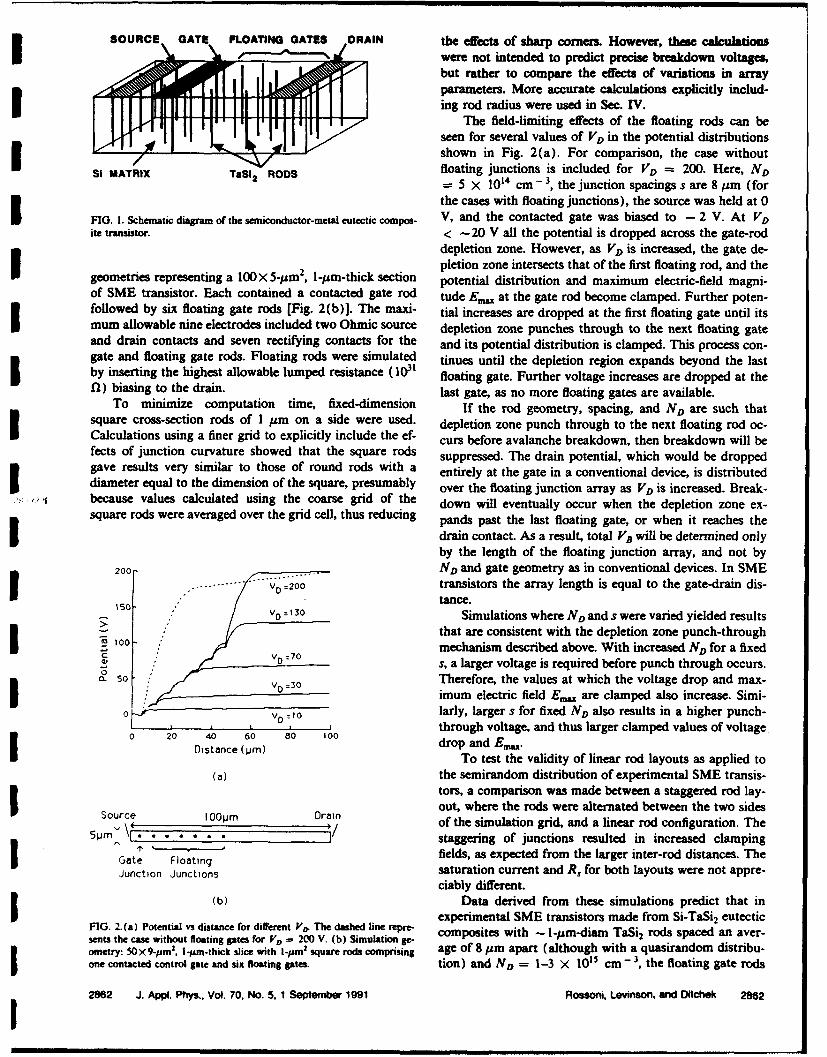
SOURCE GATE FLOATING GATES DRAIN the effects of sharp corners. However, these calculationsI were not intended to predict precise breakdown voltages,but rather to compare the effects of variations in arrayparameters. More accurate calculations explicitly includ-I ing rod radius were used in Sec. IV.
The field-limiting effects of the floating rods can beseen for several values of VD in the potential distributionsshown in Fig. 2(a). For comparison, the case without
SI MATRIX TaSI2 RODS floating junctions is included for VD = 200. Here, NDA-= 5 X 1014 cm - , the junction spacings s are 8 1Lm (forthe cases with floating junctions), the source was held at 0
FIG. 1. Schematic diagram of the semiconductor-metal eutectic compos- V, and the contacted gate was biased to -2 V. At VDite transistor. < -20 V all the potential is dropped across the gate-rod
depletion zone. However, as VD is increased, the gate de-pletion zone intersects that of the first floating rod, and the
geometries representing a 100X 5-M4m 2, 1-/Mm-thick section potential distribution and maximum electric-field magni-of SME transistor. Each contained a contacted gate rod tude Em, at the gate rod become clamped. Further poten-followed by six floating gate rods [Fig. 2(b)]. The maxi- tial increases are dropped at the first floating gate until itsmum allowable nine electrodes included two Ohmic source depletion zone punches through to the next floating gateand drain contacts and seven rectifying contacts for the and its potential distribution is clamped. This process con-gate and floating gate rods. Floating rods were simulated tinues until the depletion region expands beyond the lastby inserting the highest allowable lumped resistance (10Pt floating gate. Further voltage increases are dropped at thefl) biasing to the drain. last gate, as no more floating gates are available.
To minimize computation time, fixed-dimension If the rod geometry, spacing, and ND are such thatsquare cross-section rods of 1 Mm on a side were used. depletion zone punch through to the next floating rod oc-Calculations using a finer grid to explicitly include the ef- curs before avalanche breakdown, then breakdown will befects of junction curvature showed that the square rods suppressed. The drain potential, which would be droppedgave results very similar to those of round rods with a entirely at the gate in a conventional device, is distributeddiameter equal to the dimension of the square, presumably over the floating junction array as VD is increased. Break-because values calculated using the coarse grid of the down will eventually occur when the depletion zone ex-square rods were averaged over the grid cell, thus reducing pands past the last floating gate, or when it reaches the
drain contact. As a result, total VB will be determined onlyby the length of the floating junction array, and not by
200 ND and gate geometry as in conventional devices. In SMEVD.. 20o transistors the array length is equal to the gate-drain dis-
150 " tance.S v 0 130 Simulations where ND and s were varied yielded results
that are consistent with the depletion zone punch-throughL 1
2 :70 mechanism described above. With increased ND for a fixed0 s, a larger voltage is required before punch through occurs.
O 50 vD =30 Therefore, the values at which the voltage drop and max-imum electric field En. are clamped also increase. Simi-
0 D = 100 larly, larger s for fixed ND also results in a higher punch-through voltage, and thus larger clamped values of voltage
Distance (jam) drop and E,,.D n To test the validity of linear rod layouts as applied to(a) the semirandom distribution of experimental SME transis-
tors, a comparison was made between a staggered rod lay-
Source I n Drain out, where the rods were alternated between the two sides\prn . of the simulation grid, and a linear rod configuration. The
5m............../ staggering of junctions resulted in increased clamping* * 'fields, as expected from the larger inter-rod distances. TheGate Floating
Junction Junctions saturation current and R, for both layouts were not appre-ciably different.
(b) Data derived from these simulations predict that inexperimental SME transistors made from Si-TaSi 2 eutectic
FIG. 2. (a) Potential vs distance for different V,> The dashed line repre- xprie t lm-tiam Tasi2rodsspaced an aver:sents the case without floating gates for VD = 200 V. (b) Simulation ge- copstswh- tmdi T i2rssaednav-ometry: 50X9-tUm
2 , i1-jo-thick slice with I-)rol square rods comprising age of 8 um apart (although with a quasirandom distribu-
one contacted control gate and six floating gate. tion) and ND = 1-3 x 10s cm - 3, the floating gate rods
2862 J. Appl. Phys.. Vol. 70. No. 5, 1 September 1991 Rossoni, Levison, and Ditchek 2862

Source breakdown before the field-limiting capabilities of the float-
ing gates can take effect. Lower ND will result in a lowervoltage drop per unit distance, and therefore a larger array
Gate length for the same total V9, and lower conductance.Junctions In these calculations, round rods of radius r were usedin a square array with spacing between rods s as shown in
Cell Fig. 3. In each case, a sufficiently fine grid to accurately
represent the round rod cross sections was used. For agiven r and s, the ND that just yields breakdown when the
depletion width is equal to s was determined analytically,Floating as was the corresponding breakdown voltage per unit cell
. Junct0ons V/ The maximum voltage drop per unit length VL, wascalculated as V /L, where L, = 2r + s is the unit-cell
f length. The total breakdown voltage of the device can bedetermined as V, = VLL, where L is the array length. TheI-V characteristic was then simulated and the volume con-
Drain ductivity, o, = L/RS A, was calculated where R, is the se-
ries resistance in the on state found from the slope of the
FIG. 3. Simulation geometry with a square array of rods of radius r ad lnear region and A is the cross-sectional area of the sim-inter-rod spacing s. ulation geometry. The results are summarized in Table I.
The conductance per unit cross-sectional area, aA
= ov/L, = I/R A, wasalsocalculated.should clamp E. at a value less than that required for It may be noted that these results appear to be conser-avalanche breakdown. The maximum voltage supported by vative because the maximum ND for the case of 0.5-Amthe floating gates should be -5x 10' V/cm of gate-drain radius and 8-/um spacing is predicted to be 6x 10¹⁴
di :ance. Both these predictions are in good agreement cm- 3, although avalanche suppression was observed inwuh experimental results.'"2 experimental SME devices with approximately this geom-IV. OPTIMIZED POWER SWITCHING CAPABILITIES etry and N D = 1-3 X l015 cm-3 (Ref. 2).
- Because VB is proportional to L, arbitrarily large VBIn this section we investigate the ways in which the can, in principle, be obtained with a sufficiently long array,
floating gate array parameters can be optimized to simul- although in practice it may be limited by external factorstaneously suppress breakdown and yield high on-state con- such as surface breakdown. However, 0
'A is inversely pro-ductance. The primary requirement is that the gate deple- portional to array length. For the purposes of comparingtion zone must reach the first floating junction before floating gate array parameters, a figure of merit that isavalanche breakdown occurs. Thus, the maximum permis- independent of array length can be defined as VLO v
sible ND is determined by the condition that the depletion = VB aA. The higher this value, the higher the on-statewidth at the point where avalanche breakdown would oc- conductance, and the lower the series resistance, for a de-cur is just equal to s. Higher ND will lead to avalanche vice of a given VB,
TABLE 1. Calculated optimum carrier concentration N, breakdown voltage per unit length V1 ' series conductivity a, and VLU , for various combi-nations of rod radius r and spacing s.
r s No VL U, VLU.(/Mm) (AM) s/r (X 101s cm - ) (X to4 V/cm) (n cm) - (X lO A/cm')
2.0 0.5 0.25 83 3.6 0.69 2.51.0 0.4 0.40 110 5.9 1.93 1I0.4 0.4 1.0 93 Ii 2.65 300.5 0.5 1.0 68 10 2.48 261.0 1.0 1.0 29 9.1 1.30 122.0 2.0 1.0 13 8.1 0.73 5.9I 0.2 0.4 2.0 73 16 2.40 370.0 2.0 2.0 10 I1 0.65 7.30.1 0.4 4.0 53 18 1.68 300.25 1.0 4.0 17 15 0.82 12
0.5 2.0 4.0 7.4 13 0.51 6.61.0 4.0 4.0 3.2 II 0.26 3.00.1 1.6 16.0 4.2 I1 0.33 3.70.25 4.0 16.0 1.4 9.8 0.13 1.30.5 8.0 16.0 0.63 3.8 0.07 0.570.1 4.0 32.0 0.7 6.6 0.07 0.43
2863 J. AppI. Phys., Vol. 70. No. 5, 1 September 1991 Roesoni, Levinson, and Ditchek 2863
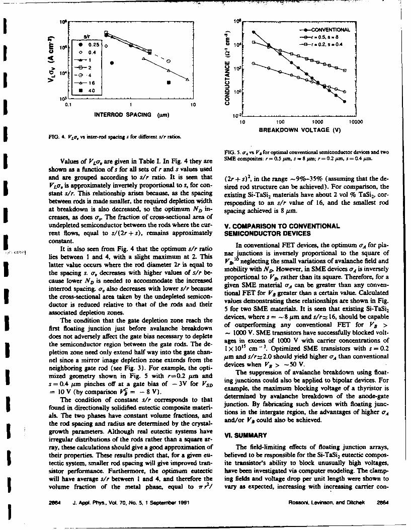
*f,0 0.-510S 10
10. 010 0 0 .4U 0U
0. 2 Q0 02
8 0101010 00
BREAKDOWN VOLTAGE (V)FIG. 4. YLO, vs inter-rod spacing s for different sir ratios.
FIG. 5. orA vs Ya for optimal conventional semiconductor devices and two
Values of VL0, are given in Table 1. In Fig. 4 they are SME composites: r = 0.51I, s = S ;an; r = 0.2 /am, s = 0.4 Am.
shown as a function of s for all sets of r and s values usedand are grouped according to sir ratio. It is seen that (2r + s) 2, in the range -9%-35% (assuming that the de-VLO'D is approximately inversely proportional to s, for con- sired rod structure can be achieved). For comparison, thestant sir. This relationship arises because, as the spacing existing Si-TaSi2 materials have about 2 vol % TaSi2, cor-between rods is made smaller, the required depletion width responding to an sir value of 16, and the smallest rodat breakdown is also decreased, so the optimum ND in- spacing achieved is 8 um.creases, as does o, The fraction of cross-sectional area ofundepleted semiconductor between the rods where the cur- V. COMPARISON TO CONVENTIONALrent flows, equal to s/(2r+s), remains approximately SEMICONDUCTOR DEVICESIconstant. I ovninlFTdvcs h piu Afrpa
It is also seen from Fig. 4 that the optimum sir ratio In conventional FET devices, the optimum GA for pla-lies between 1 and 4, with a slight maximum at 2. This nar junctions is inversely proportional to the square of
latter value occurs where the rod diameter 2r is equal to VM'° neglecting the small variations of avalanche field and
the spacing s. cr, decreases with higher values of sr be- mobility with ND. However, in SME devices A is inversely
cause lower ND is needed to accommodate the increased proportional to VB, rather than its square. Therefore, for a
interrod spacing. o, also decreases with lower sir because given SME material A can be greater than any conven-the cross-sectional area taken by the undepleted semicon- tionai FET for V, greater than a certain value. Calculated
ductor is reduced relative to that of the rods and their values demonstrating these relationships are shown in Fig.
associated depletion zones. 5 for two SME materials. It is seen that existing Si-TaSi2
The condition that the gate depletion zone reach the devices, where s =- -8 m and sir= 16, should be capable
first floating junction just before avalanche breakdown of outperforming any conventional FET for VB >
does not adversely affect the gate bias necessary to deplete - 1000 V. SME transistors have successfully blocked volt-the semiconductor region between the gate rods. The de- ages in excess of 1000 V with carrier concentrations ofpletion zone need only extend half way into the gate chan- I X 10 cm - 3. Optimized SME transistors with s = 0.2nel since a mirror image depletion zone extends from the g hm and slr= 2.0 should yield higher aA than conventional
neighboring gate rod (see Fig. 3). For example, the opti- devices when V o > a n50 V.mized geometry shown in Fig. 5 with r---0.2 /pm and The suppression of avalanche breakdown using float-s -- 0.4pm pinches off at a gate bias of - 3V for Vsd ing junctions could also be applied to bipolar devices. For
S=10.V (bycomparisonfVf a = - 8 V). example, the maximum blocking voltage of a thyristor isThe condition of constant sir corresponds to that determined by avalanche breakdown of the anode-gate
found in directionally solidified eutectic composite materi- junction. By fabricating such devices with floating junc-
als. The two phases have constant volume fractions, and tions in the intergate region, the advantages of higher A
the rod spacing and radius are determined by the crystal- andior V3 could also be achieved.growth parameters. Although real eutectic systems have VI. SUMMARYirregular distributions of the rods rather than a square ar-ray, these calculations should give a good approximation of The field-limiting effects of floating junction arrays,their properties. These results predict that, for a given eu- believed to be responsible for the Si-TaSi 2 eutectic compos-tectic system, smaller rod spacing will give improved tran- ite transistor's ability to block unusually high voltages,sistor performance. Furthermore, the optimum eutectic have been investigated via computer modeling. The clamp-
will have average sir between I and 4, and therefore the ing fields and voltage drop per unit length were shown tovolume fraction of the metal phase, equal to i r2/ vary as expected, increasing with increasing carrier con-
2864 J. Appi. Phys., Vol. 70, No. 5, 1 September 191 Rossoni, Levinson, and Dftchek 2864

centration and inter-rod spacing. It was shown that for (SDIO/IST) and managed by the Office of Naval Re-floating junction arrays, the product of maximum blocking search under contract No. N00014-86-C-0595.voltage and on-state conductivity is constant for a givenrod radius and inter-rod spacing. Optimum values of thisproduct were determined as a function of rod radius andinter-rod spacing. It was found that this product increases 'B. M. Ditchek, T. R. Middleton, P. G. Rossoni, and B. G. Yacobi,
with decreasing inter-rod spacing, and for a given spacing, Appl. Phys. Lett. 52, 1147 (1988).'M. Levinson, P. G. Rossoni, F. C. Rock, and B. M. Ditchek, Electron.
the highest values are achieved with the rod diameter Lett. 7, 777 (1990).within a factor of 2 of the inter-rod spacing, corresponding 3B. M. Ditchek, J. Hefter, T. R. Middleton, and J. Pelleg, J. Cryst.
to a rod volume fraction of -9%-35%. It was further Growth 102, 401 (1990).shown that, for a given set of array parameters and desired 4 B. M. Ditchek, B. G. Yacobi, and M. Levinson, J. Appi. Phys. 63, 1964w t(1988).maximum blocking voltage, the SME transistor could, in 'Y. C. Kao and E. D. Wolley, Proc. IEEE 55, 1409 (1967).principle, provide higher conductivity than any conven- 6M. S. Adler, V. A. K. Temple, A. P. Ferro, and R. C. Rustay, IEEEtional FET device. Trans. Electron Devices ED-24, 107 (1977).7 M. Levinson, P. G. Rossoni, S. Butler, and B. M. Ditchek (unpub-
lished).ACKNOWLEDGMENTS 'Stanford Electronics Laboratories, Stanford, CA.
9S. M. Sze and G. Gibbons, Solid-State Electron. 9, 831 (1966).This work was sponsored in part by the Strategic De- 'See, for example, K. Shenai, R. S. Scott, and B. Jayant Baliga, IEEE
fense Initiative Office/Innovative Science and Technology Trans. Electron Devices ED-36, 1811 (1989).
2865 J. Appl. Phvys., Vol. 70, No. 5, 1 Septernber 1991 Rossoni, Levinson. and Ditchek 2865

IEEE
Conference Record of the
1990 NineteenthPower Modulator Symposium
sponsored byNaval Surface Warfare CenterU.S. Army LABCOM, ET&DLAir Force Wright Research and Development CenterAir Force Weapons LaboratoryThe Electron Devices Society ofThe Institute of Electrical andElectronics Engineers, Inc.
in cooperation withThe Advisory Group on Electron Devicesand under the management ofPalisades Institute for Research Services, Inc.
Library of Congress Catalog Card No.: 89-82657 Available fromIEEE Single Copy Sales445 Hoes Lane
Piscataway, NJ 08854
Printed in USA Copyright §) 1990 by the Institute of Electrical and Electronics Engineers, Inc.345 East 47th Street, New York. NY 10017

A HIGH VOLTAGE BULK MESFET USING IN-SITU JUNCTIONS
M. Levinson, P. G. Rossoni, W. W. Byszewski, and B. M. DitchekGTE Laboratories Incorporated, Waltham, MA 02254
Abstract results using Si-TaSi2 composite devices are thenpresented which are in good agreement with the
A new bulk MESFET based on semiconductor-metal model calculations. This approach should lead toeutectic composite materials is described and its the development of devices which are capable ofapplication to pulsed power switching is discussed. both high voltage and high current in a singleNumerical modeling of these transistors has shown switch.that it should be possible to design them to holdoff very large voltages, and device and materialsparameters which should optimize their Device modelingperformance have been identified. ExperimentalSi-TaSi 2 SME devices have shown breakdown The semiconductor-metal eutectic transistorvoltages more than three times that expected for geometry [2) is shown schematically in Fig. 1(a).conventional semiconductor junctions of the same The metal rods, arrayed perpendicularly to the
* carrier concentration, in agreement with the model., wafer surface, create rectifying Schottkyjunctions with the semiconductor. A gate contact,which provides a metallic contact to the rods but
Introductik'l maintains a Schottky contact to the semiconductor,is formed between the ohmic source and drain
Extension of conventional transistor technology to contacts. Current flowing from the source to thethe pulsed power conditioning regime would require drain passes between the depletion zonesthe development of devices with "on-state" surrounding the gate rods. An external gate voltagecurrents in excess of 1 kA and blocking voltages of can be used to expand the depletion zones of the50 kV. The main obstacle to engineering such high rods accessed by the gate contact and, bypower devices is the existence of avalanche decreasing the volume of non-depletedbreakdown. It is this breakdown mechanism,together with basic junction physics, that limitsconventional devices of reasonable size to either
high voltage or high current but not both. SOURCE GATE FLOATING GATES RAIN
This paper discusses a new class of transistorsthat should allow the attainment of both highvoltage and high current in a single opening switch.They are based on the unique microstructure of a (1)new kind of electronic material: semiconductor-metal eutectic (SME) composites. These materialscontain arrays of rod-shaped metallic regionsimbedded in a single crystal semiconductor matrix.They are formed directly during crystal growthfrom the melt. The rods form parallel, cylindrical CONTROLSchottky junctions which fill the bulk of the SOUC GATE DRAINmaterial and provide the basis for a number of \ Inovel devices [1-61, including the transistors (b) 5 I Idconsidered here. I - 100 )mA
Field-effect transistors can be fabricated withthese materials which take advantage of their CONTROL FLOATINGunusual properties to overcome the limitations SOURCE GATE GATES OR IN
imposed by avalanche breakdown in conventional \ 1 . -7devices. We descnbe numerical modeling which ()I d - a a
reveals in detail the physics underlying these 100 PMavalanche-inhibiting effects and shows that hesedevices could, in principle, be designed to hold off Fig. 1. a) Semiconductor-metal eutectic transistor
arbitrarily large voltages, limited only by external geometry; geometries for PISCES simulations: b) nofactors such as surface breakdown. Experimental floating rods; c) six floating rods.
347
CH2839-9/90/0000-034"/S1.00 C) 1990 IEEE

semiconductor, reduce the source-drain current to 2provide transistor action.
One unique feature of this device is that the rods ew0t n
which lie in between the gate and drain contactsare not contacted and are therefore isolated from 1the external circuit. These junctions float inpotential in such a way as to spread the applied ant- w IMUMo1cdrain voltage over a greater distance than thewidth of a single junction. This mechanism issimilar to the well known "guard ring* effect, and .W.. t. . .can limit the maximum electric field magnitude to 0 so 100 150 200a value which is lower than the breakdown field. Drain Voltage (V)
Computer simulations of devices with and without Fig. 3. Maximum electric field vs. drain voltage forfloating rods were performed using the PISCES the geometry of Fig. 1 showing the field clampingcode [4,71. The PISCES software models two- effect of the floating gates.dimensional distributions of potential and carrierconcentrations for arbitrary device geometries andbias conditions. The version used was PISCES-1IBof Stanford Electronics Laboratories on a Digital by the PISCES software. Simulations wereVAX 11/785 mainframe computer. specified for n-type Si with uniform impurity
concentrations of 0.5 - 5 x 1015 cm"3 PISCES-lIBTwo types of simulation were performed: In the allows the placement of a simple lumpedfirst, the effect of floating junctions on device resistance on a given electrode. This capabilitybreakdown was studied. The second was aimed at was exploited to account for floating rods.optimizing material parameters and device Floating rods were simulated by specifying thegeometry for high power applications, maximum resistance (1031 fl) for each rod and
biasing it to the drain.The two basic simulation geometries are shown inFigs. 1(b) and 1(c). The conventional case, used as To simulate the operation of the transistor, thea control [Fig. 1(b)], has one gate junction close to source was held at 0 V. the gate (the first rod) wasthe source. The other case (Fig. 1(c)] has six biased to -2 V, and the drain was stepped from 0 toequally spaced floating rod-shaped junctions 200 V in 10 V increments. Potential versusbetween the gate rod and the drain. With six distance from the source is shown in Fig.2 and thefloating junctions, the simulation uses the maximum electric field magnitude versus drainmaximum number of electrodes that can be handled potential is shown in Fig. 3.comparing the two
cases with and without floating gate rods.
For the conventional case without floatingjunctions, the potential increases parabolically
200- with distance similarly to conventional planarjunctions. The maximum electric field magnitudeincreases monotonically with increasing drain
conualC3ft owl voltage. In the case with floating gate rods, thedepletion zone at the gate rod expands withincreasing drain voltage as in the conventional
Wi0l0toi at case, but only until it intersects the depletion zone
of the first floating rod. With further voltageincrease, this latter rod floats in potential so that
0, its depletion zone expands towards the next
floating rod, and the maximum electric field at the0 gate rod is clamped. Eventually, the maximum field
at the first floating rod is clamped when its*depletion zone reaches the next floating rod, and so
0 20 40 60 so 100 on. The actual value of the clamping field dependson the interrod spacing and the carrier
Distance( m)concentration, but with the proper parameters itcan be made lower than the avalanche field.
Fig. 2. Potential vs. distance from the sourcecalculated for the geometry of Fig. I at a drain The results of this model clearly indicate that thevoltage of 200 V, with and without floating gates. floating rods inhibit avalanche breakdown.
348

b Ifound at the highest carrier concentration, which
I Icorresponds to the smallest interrod spacing.
These results are important because they indicateMODEL DEVICE PARAMETERS that semiconductor-metal eutectic transistors canSMAXIMUM FIELD MAGNITUDE Emax - 105 V/cm be designed to hold off high voltages while at the
same time having relatively high carrierRod Avg. field G-D dist. for No Js concentrations and therefore high current density.
spacing at Emax Vmax-1000 (cm- 3) (A/cm 2 ) In contrast, conventional semiconductor switches(gm) (V/cm) (0m) must use low carrier concentration material to
4 5.08x10⁴ 197 5.9x10 15 6000 achieve high voltage blocking capability. They
7 5.37x10 4 186 3.3x10 15 3300 therefore require large conducting areas to provide
23 5.44x10⁴ 184 1.0x10 15 870 low on-state resistance.
Experimental Semiconductor-Metal EutecticTransistors
However. breakdown will eventually occur by apunch-through' mechanism when the depletion SME transistors were fabricated [2,3] using 500 g±m
region expands to reach the drain contact and no thick Si-TaSi2 composite wafers cut normal to theadditional floating rods are available to growth axis so that the TaSi 2 rods wereaccommodate further voltage increases. Therefore, perpendicular to the wafer surfaces. Carrierthe maxLnum blocking voltage of the device is concentrations were 1-3 x 1015 cm-3 , and thedetermined by the gate-drain spacing, rather than areal rod density was about 1.6 x 106 cm-2,the carder concentration as in conventional yielding average interrod spacing of -8 gm.devices. This distance can in principal be designedto yield an arbitrarily large blocking voltage, Wafers were thermally oxidized at 1000 C to formlimited only by external factors such as surface a 0.3 gm oxide layer. The oxide was patterned andbreakdown. opened to form central drain and concentric source
and gate contact areas as shown in Fig. 4. The gateFurther model calculations were used toinvestigate the ways that these devices could beoptimized for simultaneous high voltage and highcurrent operation. This was done by holding themaximurm electric field magnitude to a value lessthan tha: of the avalanche field, and calculating thecorresponding carrier concentration, ND, andsaturation current density, Js, for differentinterrod spacings. A microstructure with floatingrods similar to that shown in Fig. 1 was modeled todetermire the carrier concentration which yields asaturation Emax of 100 kV/cm. This maximumfield was chosen because it is conservativelybelow the value that would lead to avalanchebreakdown in silicon. The average electric fieldmagnitude in the gate-drain region and theminimum gate-drain distance needed to hold off1000 V without -punch-through" were alsocalculated. The microstructure was then scaleduniformly to different interrod spacings and roddiameters, keeping the volume fraction of the rodsconstan: (as would be the case with real eutecticsystems).:
The resz.dts are shown in Table I for interrodcenter-to-center spacings of 4, 7, and 23 pm.Although the gate-drain distances needed to hold 0.4 mmoff 1000 V are similar in all three cases and thespatially averaged field remains nearly constant atabout one-half Emax, the carrier concentrations Fig. 4. Micrograph of semiconductor-metal eutecticand saturation current densities at zero gate bias transistor, showing source and gate contactsare quite different. The highest current density is surrounding the central drain contact.
L4
contact was formed using a 0.2 jim CoSi2 layer TableJ1which maintained a Schottky barrier to the bulk Sima"]-ix while providing metallic contact to theTaS2 rods (1). Source and drain contacts consisted MEASURED AND PREDICTED BREAKDOWN VOLTAGESeither of annealed Au-Sb films or P implanted n+layers. After electrical measurements, some ND Thickness G-D Effect. V6 VBprocessed devices were successively thinned by (1015 (Lim) Dist. G-D (meas.) (predict.)mechanical polishing and remeasured, showing the cm- 3 ) (rim) Dist. (V) (V)effects of thickness on device performance. (ILm)
3 500 137 33 50 165The transfer characteristic of a typical device is 3 250 137 85 350 425shown in Fig. 5 (Ref. 3). For this carrier
concentration and interrod spacing, the modeling 3 125 137 111 600 555
resui;s indicate that the maximum electric field atthe rods will be less than the avalanche breakdown 2 500 150 46 90 230field due to the effect of the floating rods. (The 2 250 150 98 250 490model indicates that the clamping field will be -1 2 125 150 124 500 620x 105 V/cm. The avalanche field for planarjunctions of this carrier concentration is 3 x 10⁵V/cm. but the actual value will be greater due to 1 250 180 128 500 640the small volume over which the maximum field 1 125 180 154 700 770occurs in the cylindrical geometry.) We thereforeexpect that breakdown will only occur when the 1 250 62 10 40 50depletion layer punches through to the drain 1 125 250 224 1000 1120contaict where the electric field can increase to thebreakdown value. The breakdown voltage will begiven approximately by the product of the averageelectric field and the gate-drain distance. divergence will result in an effective gate-drainModeling indicates that the average field will be distance at the backside of the wafer which isabout 5 x 10⁴ V/cm. shorter than the actual contact spacing by a factor
2ttan(6), where t is the wafer thickness.Predicted and measured breakdown voltages, V, Corrected for this effect, the measured V8 are infor devices with several gate-drain spacings, reasonable agreement with the predicted values,which were successively thinned and remeasured, although still somewhat lower in all but one caseare listed in Table II. They are all lower than the as shown in Table II. However, these numbers of upvalues which would be predicted from the to 1000 V may be compared with the theoreticalcalculated average field and the actual gate-drain maximum breakdown voltage of -200 V for planarspacing. Si junctions in this- range of carrier concentration.
One effect which should lower the effective Also of interest are the current density and thebreakdown voltage is that of rod divergence [3]. switched power density. The calculated currentThe TaSi2 rods are not perfectly parallel, with a density for the 7 lim spacing device shown in Tablemaximium divergence of about +/- 60. This I is 3300 A/cm2 . The corresponding switched
power density is 1.6 x 10⁸ W/cm3 . These valuesmay be compared with up to -50 A/cm2 and -3 x10⁶ W/cm 3 observed in experimental devices with-8 gim interrod spacing. It is believed that theexperimental figures are lower both because the
1 mA/Verl iv. carrier concentrations were lower by a factor 3and because the rod distribution is not uniform.The rod distribution pattern has been shown to have
100 V/Horiz. Div. a substantial effect on current transport in thesematerials [8,91. However, the model resultsindicate the potential for high power switching of
5 vtstep devices made with improved materials.
0.2 mlv.Conclusions
The unique properties of semiconductor-metaleutectic materials can be exploited to yield a new
Fig. 5. Transfer characteristic of a typical device, class of transistors. These devices hold great
350

promise for the development of high voltage, high 2. B. M. Ditchek, T. R, Middleton, P. G. Rossoni, and B.currenL voltage controlled pulsed power switches. G. Yacobi, *Novel high voltage transistorWe have demonstrated experimental devices with fabricated using the in situ junctions in a Si-breakdown voltages far in excess of those expected TaSi2 eutectic composite,* Appl. Phys. Lett. 52,for planar junction devices made from similarly 1147 (1988).doped semiconductor material. We have alsoexplored the physics of these devices by numerical 3. B. M. Ditchek and B. G. Yacobi,modeling to identify the mechanisms which lead to "Microcharacterization and novel deviceelevated blocking voltages. The origins of these applications of semiconductor-metal eutecticeffects are now understood, and it should be composites,' Japan. J. Appl. Phys. 27, L2155possible to make SME devices which hold off (1988).arbitrarily large voltages, subject only to externalfactors such as surface breakdown. This modeling 4. M. Levinson, P. G. Rossoni, F. Rock, and B. M.work has also included a study of materials and Ditchek, 'High voltage floating gate arraydevice parameters needed to optimize both high transistor," Electron. Lett. 26, 777 (1990).voltage and high current capability in the samedevice. 5. B. M. Ditchek, B. G. Yacobi, and M. Levinson, "Novel
High Quantum Efficiency Si-TaSi2 EutecticPhotodiodes," Appl. Phys. Lett. 51, 267 (1987).
Acknowledgements6. M. Levinson, E. Eichen, P. G. Rossoni, and B. M.
The assistance of T. Middleton in material and Ditchek, "Si-TaSi2 Photodiodes With Highdevice fabrication is gratefully acknowledged. Efficiency and High Spatial Resolution from theThis work was supported in part by the Strategic UV to 1.06 g.m, Conf. on Lasers and Electro-Defense Initiative Office/Innovative Science and Optics, 1990 Tech. Digest Series Vol. 7, (Opt. Soc.Technology (SDIO/IST) and managed by the Office of of Amer., Washington, D.C.), 464 (1990).Naval Research under contract N00014-86-C-0595.
7. PISCES-IIB Stanford Electronics Laboratories,Stanford, CA, USA
References 8. B. M. Ditchek, B. G. Yacobi, and M. Levinson,"Depletion zone limited transport in Si-TaSi 2
1. B. M. Ditchek and M. Levinson, "Si-TaSi2 in situ eutectic composites,' J. Appl. Phys. 63, 1964junction eutectic composite diodes,' Appl. Phys. (1988).Lett. 49, 1656 (1986).
9. V. K. Samalam, * Si--aSi2 eutectic composites asan example of a percolation system," J. Appl.Phys. 67, 2165 (1990).
351
llgjll VULIAL.: I-LUAIINU. UAI - AHHAY these rods vary with gate bias, thus controlling the drainTRANSISTORS current.
A unicue feature of this device is the rods which lie betweenthe gate and drain. During device operation, these junctions
Indexing terms: Semiconductor devices and materials, High behave as uncontacted gates which float to potentials deter-field effects, Field effect transistors mined by the device parameters and external voltages, in a
A new high voltage field-effect transistor is described. It fea- manner similar to guard rings. To study the effects of thesetures an array of uncontacted gate elements between the floating gates, computer simulations were performed using themain gate and the drain which float so as to inhibit ava- PISCES-JIB code (Stanford Electronics Laboratories). Twolanche breakdown. Good agreement is obtained between simulation geometries were used. The first, used as a control,model predictions and the performance of experimental had one contact main gate rod of I pm square cross-sectiondevices fabricated in Si-TaSi2 semiconductor-metal eutectic adjacent to the source, as shown in Fig. lb. The other case,material. Transistors are demonstrated which hold off up to Fig. lc, has six floating gate junctions at I1pm intervals1000 V, compared with the avalanche breakdown potential of between the main gate and the drain, PISCES-JIB allows the300 V or less expected for conventional devices made with placement of a simple lumped resistance on a given electrode.similarly doped silicon. Floating junctions were simulated by inserting the maximum
resistance (10 s' 0) and biasing them to the drain. Simulationswere specified for n-type Si with uniform donor concentrationsA principal factor limiting high voltage capability in semicon- of 0.5-5 x 10t"cm- 3 . These parameters were chosen to
ductor devices is avalanche breakdown. Achieving a high approximate those of existing SME devices. Similar floatingbreakdown voltage usually requires a low carrier concentra- gate effects were observed in simulations using a range oftion and a large depletion width, Low carrier concentrations carrier concentrations and inter-rod spacings, and with stag-and large depletion widths produce high series resistance, and gered rather than in-line rod layouts.so limit on-state current densities. The potential zt the centre of the channel as a function of
We have previously demonstrated novel bulk field-effect distance from the source is shown in Fig. 2. The maximumtransistors,' as well as diodes' and photodiodes,' made withsemiconductor-metal eutectic (SME) materials. Here we showthat novel aspects of their structure can circumvent some of 200the restrictions imposed by avalanche breakdown in highvoltage devices. They present the possibility of very highvoltage switching together with high on-state current density.As unipolar devices, they should be more radiation insensitivethan bipolar devices. >- with float9ig g ones
The transistor geometry' is shown in Fig. Ia. These devices 0
are made using semiconductor-metal eutectic material which Cis grown from a melt containing a eutectic mixture of silicon 1and tantalum disilicide.' It contains a quasi-regular array of 0,
parallel rod-shaped regions of metallic TaSi, imbedded in asingle crystal silicon matrix. The TaSi 2 rods, which are orient- 0ed perpendicular to the surface of the wafer, form Schottkyjunctions with the semiconductor. The gate contact providesmetallic contacts to the rods underneath it, but maintainsa I I I I
blocking contact to the semiconductor. The depletion zones of 0 20 40 60 g0 100distance. pmr0ni
source gate floating gates drainFig. 2 Potential against distance from source
Control gate bias = - 2 VDrain bias = 200 V
electric field as a function of drain potential is shown in Fig. 3.The carrier concentration is 5 x 10icm-s, and the controlgate bias is -2V. In the case without floating gates, themaximum electric field increases monotonically with increas-
Si matrix ToS1, 2 rods ing drain voltage, as in conventional planar junctions. Whenfloating gates are incorporated, the control gate depletion
a zone expands with increasing voltage as before, but only untilit reaches the first floating gate. Beyond this point, the floating
control drain gate rises in potential as its depletion zone expands towardssource gate the next floating gate, and the maximum electric field at the
I control gate is clamped. The same maximum field is attainedat the first floating gate when its depletion zone reaches the
.- -00 i m - second floating gate, and so on. The actual value of the clamp-ing field varies with the spacing between the floating gates and
b the carrier concentration. It can be made lower than the ava-lanche field by proper design.
control floating Breakdown will eventually occur when the depletion regionsource gate gates drain expands beyond the floating gate array and no additional
\/ .. floating gates are available to accommodate further voltage5 Wm - . . - increases. At some voltage, the avalanche field will be attained
- u pm _at the last row of floating gates unless the depletion zonereaches the drain contact first and a 'punch-through' mecha-
c nism occurs. This latter effect occurs in SME transistors, asthe array length is equal to the gate-drain spacing. The
Fig. I Semiconductor-metal eutectic transistor geometry maximum blocking voltage of the device is primarily deter-a Device structure mined by the length of the floating gate array, rather than theb Control gate model carrier concentration as in conventional devices. This distancec Floating gates model can in principal be designed to yield an arbitrarily large
P.,nr;ntari frmm Fl fcTrRr)AIIrc I F7T-TFP( 7fh I,,n 1O/ 1hi 4' At- V) - 777 770

Table I MEASURED AND PREDICTED BREAKDOWN VOLTAGES
Carrier Wafer G-D Effective G-D VMS. VMXconcentration thickness distance distance measured predicted
lOScm - 3 AM an OV V
3 500 137 33 50 1653 250 137 85 350 4253 125 137 III 600 555
2 500 150 46 90 2302 250 150 98 250 4902 125 150 124 500 620
1 250 180 128 500 6401 125 180 154 700 770
1 250 62 10 40 501 125 250 224 1000 1120
correction for rod divergence. These value of up to 1000Vmay be compared with the theoretical breakdown voltage of
control gate only 100-300 V for planar Si junctions in this range of carrier con-
E centration.In summary, we have modelled and demonstrated the sup-
> pression of avalanche breakdown by floating gate arrays in-------------- semiconductor-metal eutectic field effect transistors. These
with floating gates devices can, in principle, be designed for an arbitrarily largebreakdown voltage. Good agreement was obtained betweenmodel predictions and experimental breakdown voltages,
0 . . .. . .. which were more than three times larger than those expected0 50 100 150 200 for planar junctions in silicon of the same carrier concentra-
drain voltage. V P tion.The assistance of T. Middleton in the crystal growth and
Fig. 3 Maximum electric field against drain voltage device fabrication is gratefully acknowledged. This work was
blocking voltage, limited only by external factors such as sponsored in part by the Strategic Defense Initiative Office/
surface breakdown. Innovative Science and Technology (SDIO/IST) and managedSME transistors were fabricated as previously described,' by the Office of Naval Research under contract N00014-86-C-SME tansisorsO595.
with a central drain and concentric annular gate and source
contacts. Carrier concentrations were 1-3 x 10 Scm - 3, and
the rod density was about i.6 x 106 cm-2, yielding average M. LEVINSON 24th November 1989
interrod spacing of -8pum. Different size devices were fabri- P. ROSSONIF. ROCK
cated, with gate-drain distances in the range 62-250/zm. B. M. DITCHEKFor these carrier concentrations and interrod spacings, the
model predicts that the maximum electric field will be GTE Laboratories Incorporatedclamped lower than the avalanche breakdown field. We there- 40 Sylvan Rd.fore expect that breakdown will only occur when the deple- Waltham, MA 02254, USAtion layer punches through to the drain contact. Thebreakdown voltage will be given to a good approximation bythe product of the calculated average electric field and thegate-drain distance.
One effect which lowers the effective breakdown voltage in I DITCHEK, I. M., MIDDLETON, T. R., ROSSONI, P. G., and YACOBI, B. G.:
these devices is that of rod divergence.4 The TaSi2 rods are 'Novel high voltage transistor fabricated using the in situ junctionsnot all perfectly parallel, but exhibit a maximum divergence of in a Si-TaSi2 eutectic composite', Appi. Phys. Lett., 1988, 52, pp.about ±6 °. The divergence will result in an effective gate- 1147-1149drain distance at the backside of the wafer which is shorter 2 OrrocHE, S. m, and LEVINSON. m.: Si-TaSi 2 in situ junction eutecticthan the actual contact spacing by a factor 2t tan (6), where t composite diodes', App. Phys. Lett., 1986,49, pp. 1656-1658isa the arthlcn se 3 DMW, IL M., YACODI, S. G., and LEVINSON, m.: 'Novel high
quantum efficiency Si-TaSi2 eutectic photodiodes', App. Phys.Measured and predicted breakdown voltages for devices Let, 1987,51, pp. 267-269
with several gate-drain spacings, which were successively 4 YACOW, a. I.. and DrrCHEK, B. m.: 'Characterization of multiple inthinned and remeasured, are listed in Table 1. The measured situ junctions in Si-TaSi2 composites by charge-collection micros-voltages are in good agreement with the predicted values after copy', Appl. Phys. Lett., 1987, 5, pp. 1083-1085