developing a robust memory strategy - dfr · pdf filedeveloping a robust memory strategy...
TRANSCRIPT

© 2004 – 2010 9000 Virginia Manor Rd Ste 290, Beltsville MD 20705 | 301-474-0607 | www.dfrsolutions.com
Developing a Robust Memory Strategy
Edward Wyrwas
July 28, 2016

9000 Virginia Manor Rd Ste 290, Beltsville MD 20705 | 301-474-0607 | www.dfrsolutions.com
Speaker Bio
2
Ed Wyrwas is a Senior Member of Technical Staff at DfR
Solutions. He leads DfR Solutions’ research on integrated
circuit wearout and has presented on semiconductor failure
mechanisms, device reliability and failure analysis techniques
to numerous companies, organizations and at high reliability,
space and aerospace related conferences.
His research includes characterizing semiconductor failure behavior over a
range of device types supporting automotive, aerospace and military
research programs with over 50 publications. His specialties include
designing unique accelerated test solutions, failure analysis, innovative
design and cybersecurity.
Ed participates in standards working groups for AEC, SAE, ISO and IPC.

9000 Virginia Manor Rd Ste 290, Beltsville MD 20705 | 301-474-0607 | www.dfrsolutions.com
o Memory devices are at the heart of our
digital lives from wearables to smart
phones, entertainment devices and the
cloud. The term “memory” is ubiquitous.
However, it is often forgotten that there
are many types of memory and a one-
device-fits-all approach doesn’t work.
The architecture, reliability challenges,
risks of obsolescence and level of
system integration of each type must be
considered to develop a robust memory
strategy for electronics design.
Abstract
3

9000 Virginia Manor Rd Ste 290, Beltsville MD 20705 | 301-474-0607 | www.dfrsolutions.com
o Memory types
o Reliability challenges
o Risks of obsolescence
o System integration
Agenda
4

9000 Virginia Manor Rd Ste 290, Beltsville MD 20705 | 301-474-0607 | www.dfrsolutions.com
o As an IP block (CPU, GPU, FPGA)
o As a device (SRAM, DRAM, FLASH)
o As a module (DIMM, SSD)
o In everything that runs code
Where is Memory Found?
5

9000 Virginia Manor Rd Ste 290, Beltsville MD 20705 | 301-474-0607 | www.dfrsolutions.com
o Static random-access memory (SRAM)
exists as general purpose memory or can
be integrated into a controller IC as RAM
or cache.
o Each bit is stored in a cell typically
consisting of 4 or 6 transistors.
o SRAM memories are volatile in the sense
that data is lost when the memory is not
powered.
Memory Types: SRAM
6

9000 Virginia Manor Rd Ste 290, Beltsville MD 20705 | 301-474-0607 | www.dfrsolutions.com
o Dynamic random-access memory
(DRAM) is a type of random-
access memory that stores each
bit of data in a separate
capacitor
o Capacitors are inherently leaky
and need to be refreshed
continuously to remember bit-state.
o Because of this refresh requirement, it is dynamic memory as
opposed to static random-access memory (SRAM) and other
static types of memory.
o Unlike flash memory, DRAM is volatile memory (vs. non-
volatile memory), since it loses its data quickly when power is
removed.
Memory Types: DRAM
7

9000 Virginia Manor Rd Ste 290, Beltsville MD 20705 | 301-474-0607 | www.dfrsolutions.com
o Flash memory is non-volatile in the sense that when power is removed
the stored data remains
o There are two types of Flash memory cells: NOR and NAND. This
refers to the logic gate configuration of the individual memory cells.
These types have different purposes.
o NOR Flash
o Code storage and code execution in place (XiP)
o Allows for random-access reading
o Considered fault-free because it is screened for defects
o NAND Flash
o General data storage
o Code must be copied into RAM prior to execution
o Allows only page access
o Has longer initial read access
o May contain faults as cells with defects don’t negatively impact use
Memory Types: FLASH
8

9000 Virginia Manor Rd Ste 290, Beltsville MD 20705 | 301-474-0607 | www.dfrsolutions.com
o Because NAND flash cannot execute code directly due to
its slower read performance, code is copied into the RAM
for execution.
o This is commonly referred to as a Store and Download (SnD) or the
compute memory architecture.
o In a SnD architecture, external RAM requirements increase
significantly to 512 Mb or more to shadow and execute code;
another $2 to $5 is added to the bill of material (BOM) for DRAM
memory devices, depending on density and configuration.
Memory Types: FLASH – NAND vs NOR
9

9000 Virginia Manor Rd Ste 290, Beltsville MD 20705 | 301-474-0607 | www.dfrsolutions.com
o MLCs are typically less robust then SLC flash chips in regards to the
number of program/erase (PE) cycles the device is subjected to.
o The reliability is predominately driven by the damage caused by the
tunneling electrons to the oxide layers within the individual cells.
Memory Types: FLASH – Cell Options
10
NAND NOR
Single Layer Cell > 100k PE cycles ~1M PE cycles
Multilayer Cell ≤ 100k PE cycles > 100k PE cycles

9000 Virginia Manor Rd Ste 290, Beltsville MD 20705 | 301-474-0607 | www.dfrsolutions.com
o Two general purpose types are based on the
memory access function
o Asynchronous – independent of clock frequency
o Requires a simple interface.
o Sometimes slower than synchronous as it may
introduce wait states into data transfers. However, it begins
reading/writing data once it receives instructions to do so.
o Synchronous – all timings are controlled by clock edges
o Complicated interface with internal registers that latch on each
clock edge – requires external clock.
o Allows data to be pre-fetched in a pipelined application but
sometimes requires additional clock cycles to do so.
Terminology: Access Types
11

9000 Virginia Manor Rd Ste 290, Beltsville MD 20705 | 301-474-0607 | www.dfrsolutions.com
o Interface refers to the bus architecture of a communication
system that transfers data between components
o Parallel bus carries data words concurrently on multiple
wires
o Easier to implement even though it requires extra conductors such as
clock and signals to control direction of data flow
o If an 8-bit parallel bus and a single serial bus operated at the same
clock speed, the parallel bus would be 8 times faster
o Serial bus carries data in bit-serial form
o Requires as little as two data path wires
o Can theoretically have higher data rates than parallel buses
because it inherently has no timing skew issues
Terminology: Interface Types
12

9000 Virginia Manor Rd Ste 290, Beltsville MD 20705 | 301-474-0607 | www.dfrsolutions.com
o Faster, high density memories are made with leading edge
lithography, i.e. 10nm
o There is a very limited amount of empirical data collected for
technology nodes below 50nm
o New lithography processes are introduced before previous
generations are mature
o We tend to seek the best performance, but how do we
know what the performance might be after 1, 5, even 10
years of driving?
o Performance degradation does happen, and with smaller feature
sizes, it happens in a big way
Reliability Challenges: Semiconductors
13

9000 Virginia Manor Rd Ste 290, Beltsville MD 20705 | 301-474-0607 | www.dfrsolutions.com
o Semiconductor devices do degrade and their performance can change
drastically
o Material stabilization/stress settling within crystalline structure
o Soft breakdown of films
o Damage to interface bonds and changes to threshold voltages
o In addition to normal operation (wear), transients and thermal extremes
associated with automotive environments can make lifetimes worse
o High temperatures accelerate dielectric breakdown and bias temperature instability
o Cold temperatures accelerate hot carrier effects
Reliability Challenges: Semiconductors (Cont’d)
14
DfR Solutions testing and model developmentTSMC reliability documents

9000 Virginia Manor Rd Ste 290, Beltsville MD 20705 | 301-474-0607 | www.dfrsolutions.com
o Leading edge semiconductor technology is
considered life limited by design, lithography
node and thermo-electrical conditions
o DfR Solutions has experience in developing models
for semiconductor devices in the deep sub-micron
nodes
o The semiconductor wearout multi-mechanism approach
o Utilizes semiconductor technology library data for
degradation mechanisms for materials and lithography
processes.
o Multi-mechanisms approach is the basis for SAE
ARP 6338 - Processes to assess and mitigate the
effects of early wearout in life-limited microcircuits
(LLM)
Reliability Challenges: Semiconductors (Cont’d)
15

9000 Virginia Manor Rd Ste 290, Beltsville MD 20705 | 301-474-0607 | www.dfrsolutions.com
o It is a fallacy to say that integrated circuits will not fail
because they have no moving parts. The sole reason they
work is by the movement of charge carriers (electrons and
holes) within them.
o Semiconductor scaling, in general, decreases reliability
o It is very important to consider that multiple failure
mechanisms have a simultaneous impact on the reliability
of semiconductor devices
o From our experiments, an isolated treatment of individual
aging mechanisms is insufficient to devise effective
mitigation strategies in current and next generation
semiconductor devices
Semiconductor Failures
16

9000 Virginia Manor Rd Ste 290, Beltsville MD 20705 | 301-474-0607 | www.dfrsolutions.com
o Data is limited for OEMs to appropriately assess
which components are available that will best fit their
application lifetimes
o Multi-Mechanism Approach is targeted towards OEMs
o Limited resources available to OEMs on integrated circuit
design and reliability
o Need to perform prediction with system-level design criteria
(electrical and thermal data) and component documentation
such as its datasheet
o Foundries typically keep acceleration models confidential
Multi-Mechanism Approach
17

9000 Virginia Manor Rd Ste 290, Beltsville MD 20705 | 301-474-0607 | www.dfrsolutions.com
o Key assumptions in this methodology
o Use of qualification test data in lieu of device time-to-failure
data
o Academic sub-circuit designs to analyze transistor stress states
within functional blocks
o Single process node selection for each device
o Basic incorporation of redundancy and/or error correction
techniques used in components
Multi-Mechanism Approach (Cont’d)
18

9000 Virginia Manor Rd Ste 290, Beltsville MD 20705 | 301-474-0607 | www.dfrsolutions.com
o Fabrication mechanism
o Electromigration is typically designed out of
the device using design verification rules and
well known models containing physical
properties of the conductors
o Aging mechanisms
o Dielectric breakdown can occur in interlayer
dielectrics and in the gate stack
o Bias temperature instability is a function of
fabrication and physical material interfaces
o Hot carrier effects take place randomly but
occur when the semiconductor is active
Degradation Mechanisms
19
EDA & DVT

9000 Virginia Manor Rd Ste 290, Beltsville MD 20705 | 301-474-0607 | www.dfrsolutions.com
o DfR Solutions uses its multi-mechanism approach to
calculate the failure rates of leading edge integrated
circuits for OEMs and component manufacturers
o Semiconductor parametric information down to 10nm planar
and 14nm FinFET
o Results are in line with 2000 to 6000 FIT per DRAM
memory devices reported by Google / University of
Toronto
Memory Failure Rate Calculation
20
1 MB DRAM cell 0.19 FIT
1 GB DRAM chip 185 FIT
32 GB DRAM Array 5920 FIT

9000 Virginia Manor Rd Ste 290, Beltsville MD 20705 | 301-474-0607 | www.dfrsolutions.com
o Failure of a SSD is dependent on the
integrity of individual FLASH cells.
o Cells containing multiple bits fail sooner
than single layer cells when operated
using the same program/erase profile
o Geometrically smaller cells (from feature
scaling) tend to fail sooner than larger
cells due to stress induced leakage
current and dielectric breakdown
o Higher junction temperatures
cause larger amounts of
leakage current leading to
earlier-than-anticipated device
failure
Solid State Drives (SSD)
21

9000 Virginia Manor Rd Ste 290, Beltsville MD 20705 | 301-474-0607 | www.dfrsolutions.com
Solid State Drive Integrity
22

9000 Virginia Manor Rd Ste 290, Beltsville MD 20705 | 301-474-0607 | www.dfrsolutions.com
o Failure rates are in line with
reported failure rates by
Facebook and Google
o Facebook reports annual failure rates
between 4 and 34%
o Google reported four year failure
rates between 11% and 42%
SSD Reported Failure Rates
23

9000 Virginia Manor Rd Ste 290, Beltsville MD 20705 | 301-474-0607 | www.dfrsolutions.com
o Most of the current packaging is to package
single devices such as Intel’s processors for
PCs and laptops
o Traditional packaging offers minimal value to
high performance applications (microprocessor BGA,
memory BGA, and so on)
o The best packaging seems to be no packaging
and assembly at all – the dawn of chip-first or
embedded packaging such as system in package (SiP) or multi-chip
packages
o Georgia Tech calls this next era of integration System Moore’s Law
o The end goal of system scaling is to enable entire system-
on-one single package
o The concept is a 3D system package based on system scaling and
heterogeneous integration
Reliability Challenges: Packages
24

9000 Virginia Manor Rd Ste 290, Beltsville MD 20705 | 301-474-0607 | www.dfrsolutions.com
o Copper interconnects through a
typical BGA substrate don’t work
o Copper scaling from 45nm to the 7nm
node (planar) causes resistance
increases of almost 50%
o Through silicon vias (TSVs) make
cutting edge performance possible
o Improved performance from ultra-short
interconnections using 2.5D and 3D
integration – upwards of 1 TB/s
bandwidth
Reliability Challenges: Packages (Cont’d)
25
CoWoS

9000 Virginia Manor Rd Ste 290, Beltsville MD 20705 | 301-474-0607 | www.dfrsolutions.com
o If multiple chips are to be utilized, then keeping them as
close as possible will save on performance
o We achieve this with 2.5D and 3D integration. This is different from
multi-chip modules in that there is not an FR4 substrate to fan-out the
interconnects; rather, silicon is used
Reliability Challenges: Packages (Cont’d)
26

9000 Virginia Manor Rd Ste 290, Beltsville MD 20705 | 301-474-0607 | www.dfrsolutions.com
3D Structures
27
Source: micron

9000 Virginia Manor Rd Ste 290, Beltsville MD 20705 | 301-474-0607 | www.dfrsolutions.com
Thermomechanical Challenges
28
*
* Flip chip multi chip package

9000 Virginia Manor Rd Ste 290, Beltsville MD 20705 | 301-474-0607 | www.dfrsolutions.com
Evolution of Higher Densities
29

9000 Virginia Manor Rd Ste 290, Beltsville MD 20705 | 301-474-0607 | www.dfrsolutions.com
o Package material comparisons can be made using
Sherlock Automated Design AnalysisTM
o Sherlock can assess the package using its high-fidelity
modeling capability
Packages Suitable for Your Design
30

9000 Virginia Manor Rd Ste 290, Beltsville MD 20705 | 301-474-0607 | www.dfrsolutions.com
o Die stacking can cause thermal
issues because of the lack of a
readily accessible thermal
dissipation channel compared
with a single chip in a package
on the PCB.
o As such, thermal vias or
additional through silicon
vias (TSVs) are necessary to
conduct the heat for 3D IC architectures
A Well Understood Challenge
31

9000 Virginia Manor Rd Ste 290, Beltsville MD 20705 | 301-474-0607 | www.dfrsolutions.com
A Well Understood Challenge (Cont’d)
32

9000 Virginia Manor Rd Ste 290, Beltsville MD 20705 | 301-474-0607 | www.dfrsolutions.com
o Even FinFETs generate more localized heat
o A 16nm FinFET has 25% more drive capability compared with a 20nm
planar transistor, plus a higher gate density.
o This results in 25% to 30% more power density in a local area. That
translates to a higher local self-heat.
o Self-heat means that the temperature increases in the local area due to the
power. That’s combined with the thermal boundary conditions for the device
and also for the chip.
A Well Understood Challenge (Cont’d)
33

9000 Virginia Manor Rd Ste 290, Beltsville MD 20705 | 301-474-0607 | www.dfrsolutions.com
o Conductor scaling includes vias
o Norman Chang, vice president of product strategy at Ansys-Apache
o “The via electromigration (EM) limit decreases 20% per
generation.”
o “With all these factors combined together we will have more
severe thermal issues, regardless if it is on a single chip for 16nm
or below, or for 3D IC designs.”
A Well Understood Challenge (Cont’d)
34

9000 Virginia Manor Rd Ste 290, Beltsville MD 20705 | 301-474-0607 | www.dfrsolutions.com
o DfR Solutions recommends assessing the thermal
response of memory devices in the same way as a
computer server
o There are three potential thermal cycles that a server
can experience
o Mini-cycles due to fluctuations in computational loading
o Drift in cold aisle temperature due to free air cooling (local
environment)
o Power down for energy savings or maintenance (system
configuration and usage)
Recommended Simulation Environment
35

9000 Virginia Manor Rd Ste 290, Beltsville MD 20705 | 301-474-0607 | www.dfrsolutions.com
o A server OEM performed an extensive thermal survey
of servers and switches in a typical data center
o Based on typical data center traffic, the OEM
ran their analysis and
measurements for a box
at 25% of maximum
processing load
(utilization)
o This is in line with an
analysis of Amazon Cloud
CPU Utilization performed
by Accenture and reporting
by The Uptime Institute (<20%)
Typical Server Environment
36

9000 Virginia Manor Rd Ste 290, Beltsville MD 20705 | 301-474-0607 | www.dfrsolutions.com
o Mini Cycles
o Mini-cycles are changes in box-level temperatures (inside the box,
but not necessarily component specific) due to variations in load
experienced by the server and adjacent computer hardware
o The 80th percentile of the server population will experience 10 mini-
cycles per day
o Typical mini-cycle is between 10-15C
o Cold Aisle Drift
o Server OEM measured an average 2C delta for 140 days/year
o Power Down
o A typical server is powered down once a year. 20% of servers are
powered down once a month
Recommended Server Environment
37

9000 Virginia Manor Rd Ste 290, Beltsville MD 20705 | 301-474-0607 | www.dfrsolutions.com
o Identify other long life industries and leverage their
technologies. Best opportunities seem to be with
automotive and telecom.
o Automotive electronics
o Required by U.S. Law to maintain replacement parts for 10
years from the original date of manufacture1– extends life cycle
to 25 years in some cases.
o Telecommunication infrastructure
o Service life of Integrated Services Digital Network (ISDN) and
mobile-based networks (i.e. GSM, CDMA) is typically 10-15 to
25 years.
o Mobile computing devices
o Just a few companies are responsible for >80% of the
component purchases; most with product lifetimes ranging from
2-3 years.
Strategies to Avoid Obsolescence
38

9000 Virginia Manor Rd Ste 290, Beltsville MD 20705 | 301-474-0607 | www.dfrsolutions.com
o Managing obsolescence risks of discrete devices
o Dramatic reduction in market size
o Devices have transitioned to embedded IP blocks
o Mitigations include selecting forward compatible device types with
universal footprints
o The 48-BGA is a common footprint for both small and large capacity
memory devices. The pin-outs remain the same despite the increased
memory address space
o Addressing is controlled by the interface type and bus bandwidth
o Memory densities increase due to scaling of the process technology
o An interposer or fan-out breakout board can be used to convert the
footprint of functionally-compatible memory devices
o Assumes the same bandwidth and interface type is used (pin out would
include power, ground, data lines and control lines)
o Significant supply chain available
Obsolescence Challenges
39

9000 Virginia Manor Rd Ste 290, Beltsville MD 20705 | 301-474-0607 | www.dfrsolutions.com
o SRAM market size is shrinking
o Driven by integration of SRAM
into microprocessors and mobile
device processors
o Discrete devices still have a niche
market in high performance
synchronous SRAM
o Gartner Dataquest divides the SRAM market into segments based on
speed. The highest performance segment is comprised of SRAMs that
operate at speeds of less than 10 nanoseconds. “Very Fast SRAMs”
are predominantly utilized in high-performance networking and
telecommunications equipment.
Obsolescence Risks by Type: SRAM
40
http://www.fool.com/investing/general/2014/01/27/cypress-semiconductors-ceo-says-bring-on-the-compe.aspx

9000 Virginia Manor Rd Ste 290, Beltsville MD 20705 | 301-474-0607 | www.dfrsolutions.com
o Some uncertainty about the current state and future growth of NOR
flash memory
o However, none of the trends indicate a significant reduction in revenue
o Market share is declining rapidly more due to rapid increase in NAND than
a decrease in NOR
o Indicates that NOR is not following traditional obsolescence life cycle
o Driven by market leader in mobile devices with a transition towards the
rising demand for wearables
Obsolescence Risks by Type: NOR
41

9000 Virginia Manor Rd Ste 290, Beltsville MD 20705 | 301-474-0607 | www.dfrsolutions.com
o Disagreements regarding NOR Flash market size is driven by
uncertainty in the machine-to-machine (M2M) communications market
o Used in wearables, the smart power grid space and in connected homes
o Cisco and Gartner project the Internet of Things (IoT) to reach a $1.9 trillion
global value by 2020
o Boot ROMs, such as BIOS chips, for most device types will use NOR
Flash
o Network attached storage, cell phones, e-readers, GPS/Navigation,
handheld devices, industrial sensors, smart TVs, game consoles, etc.
Obsolescence Risks by Type: NOR
42

9000 Virginia Manor Rd Ste 290, Beltsville MD 20705 | 301-474-0607 | www.dfrsolutions.com
o Process technology changes should not impact the
availability of comparable devices because
advancements in device packages will compensate
o Smaller technology nodes, however, will increase the
reliability risks in regards to semiconductor
degradation mechanisms and data retention lifetimes
o Devices below the 130nm technology node may experience
risks of early failure due or performance instabilities from
dielectric breakdown and hot carrier effects
o Data retention of any flash refers to its ability to retain its
programmed state. Flash data retention is known to degrade
over time due to temperature and stress induced leakage
current (SILC)
Obsolescence Risks from Process Technology
43

9000 Virginia Manor Rd Ste 290, Beltsville MD 20705 | 301-474-0607 | www.dfrsolutions.com
o For interface type, the general
trend is most new controllers and
chipsets are designing SPI
interfaces. The overall trend will
be that SPI will continue to grow
in market share and parallel will
decrease
o Trends show individual parallel devices are used versus multiple
serial devices; serial devices can be daisy-chained
o Parallel devices cost more per unit than serial devices
o As of 2016, speeds of serial devices have begun to
overcome those of parallel devices (except for DRAM)
Obsolescence Risks by Interface
44

9000 Virginia Manor Rd Ste 290, Beltsville MD 20705 | 301-474-0607 | www.dfrsolutions.com
o Memory capacities per chip increase with each
generation
o This is not an obsolescence risk, as additional memory
space can go unused
Obsolescence Risks for Capacity
45

9000 Virginia Manor Rd Ste 290, Beltsville MD 20705 | 301-474-0607 | www.dfrsolutions.com
o Speed grade goes through a much slower technology
refresh
o Speed grade refers to the random access time
o Existing categories range from 8ns to 110ns
o Will only get faster
o Should not be a risk, because this is a ‘not to exceed’
value
o Memory devices with higher speed grades are drop in
replacements for memories with lower speed grades
o The memory device must be compatible with the system clock
o E.g. 40 MHz clock → 25ns bus clock period (TBCYC)
Suppose the ASIC memory interface timing is 28ns (TMRAC)
Access time must be ≤ 3*TBCYC – TMRAC, which is 47ns
Obsolescence Risks by Speed Grade
46

9000 Virginia Manor Rd Ste 290, Beltsville MD 20705 | 301-474-0607 | www.dfrsolutions.com
o No indication of a downwards
trend in bus width, though
insertion is stabilizing
o Worst case, it should not be a
risk as you can access an 8-bit
word using a 16-bit bus
o Bus width is defined by the
processor
o As long as memory addresses are
correctly aligned (often referred
to as an offset), you will access
the correct data
Obsolescence Risks for Bus Width
47

9000 Virginia Manor Rd Ste 290, Beltsville MD 20705 | 301-474-0607 | www.dfrsolutions.com
o Miniaturization of microelectronic devices has kept
the industry on track with projections from Moore’s
Law. As devices have been scaled
to smaller technology nodes, so has
the supply voltage.
o Obsolescence risks exists for
5.0V devices.
o The majority of devices are standardized to a
voltage range from 1.8V – 3.3V, though trends
show next generation devices ≤1.35V.
Obsolescence Risks by Input Voltage
48

9000 Virginia Manor Rd Ste 290, Beltsville MD 20705 | 301-474-0607 | www.dfrsolutions.com
o Organization of bits in memory
o Mitigating memory corruption
o Redundancy
o Error Correction
System Integration
49

9000 Virginia Manor Rd Ste 290, Beltsville MD 20705 | 301-474-0607 | www.dfrsolutions.com
Memory Organization
50
Memory (set of pages)
Page (set of blocks)
Block (set of words)
Words contain bytes
Bytes contain bits

9000 Virginia Manor Rd Ste 290, Beltsville MD 20705 | 301-474-0607 | www.dfrsolutions.com
NAND – Formatted Memory Organization
51
Data
write
1 2 3 4 5 6 7 8
Memory is written to the next available
page as instructed to by the configuration
If no pages are available, the memory is
logically full
1 2 3 4 5 6 7 81 2 3 4 5 6 7 81 2 3 4 5 6 7 81 2 3 4 5 6 7 81 2 3
1 2 3 4 5 6 7 81 2 3 4 5 6 7 81 2 3 4 5 6 7 81 2 3 4 5 6 7 81 2 3 4 5
Empty cells can exist, but if the unallocated space isn’t large enough to
contain a full memory write, it is ignored during that write routine
In the typical I/O stack (disk drives), fragmented data can be written to these
addresses at a later time

9000 Virginia Manor Rd Ste 290, Beltsville MD 20705 | 301-474-0607 | www.dfrsolutions.com
Writing RAW to a Formatted Space
52
Data
write
High level view of the how the SD card is formatted
1 2 3Data
write
High level view of what the microcontroller thinks it is doing
High level view of what it’s actually doing
Data
write
1 2 3 4 5 6 7 8
Pages are misaligned between what is written and how it is formatted

9000 Virginia Manor Rd Ste 290, Beltsville MD 20705 | 301-474-0607 | www.dfrsolutions.com
Writing RAW to a Formatted Space
53
1 2 3 4 5 6 7 8
Let’s assume that each write to the
memory takes up a full page. This results
in this depiction.
When the controller checks for bad blocks, each of these misalignments
causes the blocks within the pages to be identified as ‘bad’ (whether they
are or aren’t)
1 2 3 4
n
etc.
{Volume} view
9000 Virginia Manor Rd Ste 290, Beltsville MD 20705 | 301-474-0607 | www.dfrsolutions.com
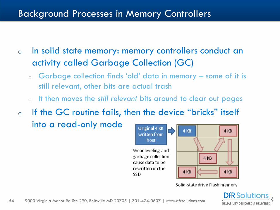
o In solid state memory: memory controllers conduct an
activity called Garbage Collection (GC)
o Garbage collection finds ‘old’ data in memory – some of it is
still relevant, other bits are actual trash
o It then moves the still relevant bits around to clear out pages
o If the GC routine fails, then the device “bricks” itself
into a read-only mode
Background Processes in Memory Controllers
54

9000 Virginia Manor Rd Ste 290, Beltsville MD 20705 | 301-474-0607 | www.dfrsolutions.com
o There are many challenges ahead
o Semiconductor and package scaling have increased
reliability/durability risks.
o New thermal challenges are arising from higher density
packages and circuit card modules.
o There are manageable risks of obsolescence from package
scaling and the transition to embedded devices.
o These challenges are manageable by applying best
practices in design for reliability early in the lifecycle
o Thermomechanical evaluation, simulation and degradation
testing should be performed to assess the integrity of the
device in terms of data handling and retention in the
anticipated environment.
Conclusion
55

© 2004 – 2010 9000 Virginia Manor Rd Ste 290, Beltsville MD 20705 | 301-474-0607 | www.dfrsolutions.com
Thank you
Edward Wyrwas
1-301-640-5816
56